US10075104B2 - Plasmonic nanostructures for conversion of optical power to electrical power - Google Patents
Plasmonic nanostructures for conversion of optical power to electrical power Download PDFInfo
- Publication number
- US10075104B2 US10075104B2 US13/679,995 US201213679995A US10075104B2 US 10075104 B2 US10075104 B2 US 10075104B2 US 201213679995 A US201213679995 A US 201213679995A US 10075104 B2 US10075104 B2 US 10075104B2
- Authority
- US
- United States
- Prior art keywords
- plasmonic
- nanostructure
- nanostructures
- plasmoelectric
- irradiation
- Prior art date
- Legal status (The legal status is an assumption and is not a legal conclusion. Google has not performed a legal analysis and makes no representation as to the accuracy of the status listed.)
- Active, expires
Links
- 239000002086 nanomaterial Substances 0.000 title claims abstract description 353
- 230000003287 optical effect Effects 0.000 title claims abstract description 80
- 238000006243 chemical reaction Methods 0.000 title claims abstract description 68
- 238000012546 transfer Methods 0.000 claims abstract description 51
- 239000002105 nanoparticle Substances 0.000 claims description 27
- 239000000463 material Substances 0.000 claims description 20
- 239000002184 metal Substances 0.000 claims description 19
- 229910052751 metal Inorganic materials 0.000 claims description 19
- 230000008859 change Effects 0.000 claims description 17
- 239000004020 conductor Substances 0.000 claims description 11
- 230000007423 decrease Effects 0.000 claims description 11
- 230000008878 coupling Effects 0.000 claims description 10
- 238000010168 coupling process Methods 0.000 claims description 10
- 238000005859 coupling reaction Methods 0.000 claims description 10
- 239000011159 matrix material Substances 0.000 claims description 8
- 238000010521 absorption reaction Methods 0.000 description 92
- 239000002245 particle Substances 0.000 description 61
- 230000005855 radiation Effects 0.000 description 57
- 239000010931 gold Substances 0.000 description 47
- 230000000694 effects Effects 0.000 description 27
- 230000007935 neutral effect Effects 0.000 description 20
- 230000004044 response Effects 0.000 description 20
- 238000004654 kelvin probe force microscopy Methods 0.000 description 18
- 238000000034 method Methods 0.000 description 16
- 239000000523 sample Substances 0.000 description 16
- 238000001228 spectrum Methods 0.000 description 14
- 230000003595 spectral effect Effects 0.000 description 13
- 230000005284 excitation Effects 0.000 description 12
- 230000001965 increasing effect Effects 0.000 description 12
- 239000004065 semiconductor Substances 0.000 description 10
- 238000003491 array Methods 0.000 description 9
- 238000012932 thermodynamic analysis Methods 0.000 description 9
- 238000004458 analytical method Methods 0.000 description 8
- 238000013459 approach Methods 0.000 description 8
- 239000003795 chemical substances by application Substances 0.000 description 8
- 239000000084 colloidal system Substances 0.000 description 7
- 238000010586 diagram Methods 0.000 description 7
- 238000005259 measurement Methods 0.000 description 7
- FAPWRFPIFSIZLT-UHFFFAOYSA-M Sodium chloride Chemical compound [Na+].[Cl-] FAPWRFPIFSIZLT-UHFFFAOYSA-M 0.000 description 6
- 238000000862 absorption spectrum Methods 0.000 description 6
- 230000001419 dependent effect Effects 0.000 description 6
- 230000008901 benefit Effects 0.000 description 5
- 239000000243 solution Substances 0.000 description 5
- 230000005676 thermoelectric effect Effects 0.000 description 5
- 230000003247 decreasing effect Effects 0.000 description 4
- 239000003989 dielectric material Substances 0.000 description 4
- 238000005421 electrostatic potential Methods 0.000 description 4
- 239000003574 free electron Substances 0.000 description 4
- 150000002739 metals Chemical class 0.000 description 4
- 238000000089 atomic force micrograph Methods 0.000 description 3
- 238000004630 atomic force microscopy Methods 0.000 description 3
- 230000004888 barrier function Effects 0.000 description 3
- 239000008151 electrolyte solution Substances 0.000 description 3
- 230000005281 excited state Effects 0.000 description 3
- PCHJSUWPFVWCPO-UHFFFAOYSA-N gold Chemical compound [Au] PCHJSUWPFVWCPO-UHFFFAOYSA-N 0.000 description 3
- 229910052737 gold Inorganic materials 0.000 description 3
- 238000010438 heat treatment Methods 0.000 description 3
- 230000010355 oscillation Effects 0.000 description 3
- 230000002441 reversible effect Effects 0.000 description 3
- 239000011780 sodium chloride Substances 0.000 description 3
- 239000000758 substrate Substances 0.000 description 3
- XLYOFNOQVPJJNP-UHFFFAOYSA-N water Substances O XLYOFNOQVPJJNP-UHFFFAOYSA-N 0.000 description 3
- 238000000149 argon plasma sintering Methods 0.000 description 2
- 229920002678 cellulose Polymers 0.000 description 2
- 239000001913 cellulose Substances 0.000 description 2
- 239000002772 conduction electron Substances 0.000 description 2
- 238000013461 design Methods 0.000 description 2
- 239000002784 hot electron Substances 0.000 description 2
- 238000005286 illumination Methods 0.000 description 2
- 239000012212 insulator Substances 0.000 description 2
- 239000000203 mixture Substances 0.000 description 2
- 238000012986 modification Methods 0.000 description 2
- 230000004048 modification Effects 0.000 description 2
- 230000005693 optoelectronics Effects 0.000 description 2
- 230000010287 polarization Effects 0.000 description 2
- 229920000728 polyester Polymers 0.000 description 2
- 238000011160 research Methods 0.000 description 2
- 229910052709 silver Inorganic materials 0.000 description 2
- 238000001069 Raman spectroscopy Methods 0.000 description 1
- BQCADISMDOOEFD-UHFFFAOYSA-N Silver Chemical compound [Ag] BQCADISMDOOEFD-UHFFFAOYSA-N 0.000 description 1
- 230000006978 adaptation Effects 0.000 description 1
- 239000002156 adsorbate Substances 0.000 description 1
- 239000007864 aqueous solution Substances 0.000 description 1
- 230000008033 biological extinction Effects 0.000 description 1
- 238000004364 calculation method Methods 0.000 description 1
- 239000003990 capacitor Substances 0.000 description 1
- 230000001427 coherent effect Effects 0.000 description 1
- 239000013068 control sample Substances 0.000 description 1
- 238000013016 damping Methods 0.000 description 1
- 238000011161 development Methods 0.000 description 1
- 238000009792 diffusion process Methods 0.000 description 1
- 239000000975 dye Substances 0.000 description 1
- 230000005686 electrostatic field Effects 0.000 description 1
- 230000023266 generation of precursor metabolites and energy Effects 0.000 description 1
- AMGQUBHHOARCQH-UHFFFAOYSA-N indium;oxotin Chemical compound [In].[Sn]=O AMGQUBHHOARCQH-UHFFFAOYSA-N 0.000 description 1
- 230000001939 inductive effect Effects 0.000 description 1
- 238000002329 infrared spectrum Methods 0.000 description 1
- 238000002372 labelling Methods 0.000 description 1
- 230000007246 mechanism Effects 0.000 description 1
- 239000002082 metal nanoparticle Substances 0.000 description 1
- 239000002077 nanosphere Substances 0.000 description 1
- 238000005457 optimization Methods 0.000 description 1
- 230000008569 process Effects 0.000 description 1
- 238000000926 separation method Methods 0.000 description 1
- 239000004332 silver Substances 0.000 description 1
- 238000006467 substitution reaction Methods 0.000 description 1
- 230000009897 systematic effect Effects 0.000 description 1
- 238000001429 visible spectrum Methods 0.000 description 1
Images


Classifications
-
- H—ELECTRICITY
- H02—GENERATION; CONVERSION OR DISTRIBUTION OF ELECTRIC POWER
- H02N—ELECTRIC MACHINES NOT OTHERWISE PROVIDED FOR
- H02N3/00—Generators in which thermal or kinetic energy is converted into electrical energy by ionisation of a fluid and removal of the charge therefrom
-
- H02N6/00—
-
- B—PERFORMING OPERATIONS; TRANSPORTING
- B82—NANOTECHNOLOGY
- B82Y—SPECIFIC USES OR APPLICATIONS OF NANOSTRUCTURES; MEASUREMENT OR ANALYSIS OF NANOSTRUCTURES; MANUFACTURE OR TREATMENT OF NANOSTRUCTURES
- B82Y30/00—Nanotechnology for materials or surface science, e.g. nanocomposites
-
- H—ELECTRICITY
- H02—GENERATION; CONVERSION OR DISTRIBUTION OF ELECTRIC POWER
- H02S—GENERATION OF ELECTRIC POWER BY CONVERSION OF INFRARED RADIATION, VISIBLE LIGHT OR ULTRAVIOLET LIGHT, e.g. USING PHOTOVOLTAIC [PV] MODULES
- H02S99/00—Subject matter not provided for in other groups of this subclass
-
- Y—GENERAL TAGGING OF NEW TECHNOLOGICAL DEVELOPMENTS; GENERAL TAGGING OF CROSS-SECTIONAL TECHNOLOGIES SPANNING OVER SEVERAL SECTIONS OF THE IPC; TECHNICAL SUBJECTS COVERED BY FORMER USPC CROSS-REFERENCE ART COLLECTIONS [XRACs] AND DIGESTS
- Y02—TECHNOLOGIES OR APPLICATIONS FOR MITIGATION OR ADAPTATION AGAINST CLIMATE CHANGE
- Y02E—REDUCTION OF GREENHOUSE GAS [GHG] EMISSIONS, RELATED TO ENERGY GENERATION, TRANSMISSION OR DISTRIBUTION
- Y02E10/00—Energy generation through renewable energy sources
- Y02E10/50—Photovoltaic [PV] energy
Definitions
- the present invention relates generally to devices and methods for conversion of optical power into electrical power by plasmonic nanostructures. More particularly, the invention relates to plasmoelectric devices for improved conversion efficiency of optical power to electrical power using resonant optical absorption in plasmonic nanostructures, and to methods of power conversion using resonant optical absorption in plasmonic nanostructures.
- Plasmonic materials are metals or metal-like materials in which valence electrons are able to move freely.
- Common plasmonic materials include gold (Au) and silver (Ag).
- incident light e.g., from a light beam
- stimulated valence electrons on the surface of the material collectively ripple to create electromagnetic waves on the boundary between the surface of the material and the surrounding medium (e.g., air or water).
- Resonance occurs when the frequency of photons in the incident light matches the natural frequency of the oscillating surface electrons in the material.
- the response amplitude of an object or device composed of plasmonic material reaches a maximum at the resonance frequency (or wavelength).
- Plasmonic nanostructures are objects or devices of a nanoscale size (e.g., an intermediate size between microscopic- and molecular-sized objects) that are composed of plasmonic material. Plasmonic nanostructures exhibit high internal energy density when irradiated with light. This high internal energy density arises from the coupling of their resonant free electron oscillations to the incident light. Plasmonic nanostructures can also be spectrally tailored. For example, the plasmonic resonance of nanostructures can be tuned from the ultraviolet through the visible and infrared spectrum based on design parameters such as the size, shape and architecture of the plasmonic nanostructures, which influence the excitation and propagation of plasmons.
- plasmonic nanostructures have been the subject of scientific research relating to various fields and topics, including subwavelength optical confinement, nanoscale photonic circuits, concentration schemes for photovoltaics, field enhancement for Raman spectroscopy, biological labeling techniques, and metamaterials.
- This poor power conversion efficiency is due in part to the optical behavior of metals and other plasmonic materials, which are characterized by large free carrier density.
- One of the primary reasons for the low optical-to-electrical power conversion efficiency is the very short excited state lifetime of electrons in metals and other conductors, which is usually less than 10 fs.
- Embodiments of the present invention address the problem of low optical-to-electric power conversion efficiency by taking advantage of a distinctive property of plasmonic nanostructures, namely that charge transport can be induced solely by changes in their internal charge density. This distinctive behavior is described herein as the “plasmoelectric effect.”
- the plasmoelectric effect induces “plasmoelectric potentials” in the nanostructures.
- irradiation at frequencies other than the resonance frequencies (known as “off-resonant irradiation”) of the nanostructures is one approach to inducing charge transfer.
- a power conversion device may be designed to maximize the plasmoelectric potential difference and current generated between the nanostructures (thereby increasing power conversion efficiency), by using strategic device geometry and an incident radiation profile to influence the internal charge density of the nanostructures.
- a plasmoelectric device for conversion of optical power to direct current (DC) electrical power has multiple parameters that can be varied so as to produce a plasmoelectric potential and generate current for use by an external circuit.
- Embodiments of the present invention relate to different permutations of the various parameters, each of which will create a change, or delta, in the internal charge densities of the nanostructures for the purpose of producing a plasmoelectric potential and generating a current.
- such parameters may include similarities or differences between electrically coupled nanostructures, such as the size of nanostructures (e.g., radius or diameter), the arrangement of the nanostructures (e.g., a plurality of arrays of electrically coupled nanostructures), and the type of nanostructures (e.g., which plasmonic materials are used).
- Such parameters may also relate to the incident irradiation profile, such as the frequency and intensity of the incident light. For example, different incident frequencies may be used for each nanostructure in a device, or the same frequency may be used for all nanostructures in a device. The incident frequencies may be resonant frequencies or off-resonant frequencies.
- charge transport (and thus plasmoelectric potential and current generation) depends primarily on the internal charge densities of the electrically coupled nanostructures, no additional semiconductor or insulating components are needed to rectify the excited electrons and perform power conversion.
- semiconductor or insulating components are used in typical power conversion schemes, the high energy density of the optically excited electrons cannot be fully harnessed because of electronic relaxation that occurs when excited electrons couple to phonons in the metal and relax before they can exit the plasmonic nanostructure to perform work on circuit load.
- an all-metal, or all-conductor, circuit without semiconductor or insulating components may be employed to convert optical power to electric power.
- the power conversion efficiency of a plasmoelectric device is not limited by the short excited state lifetime of optically excited electrons.
- a plasmoelectric device for conversion of optical power to DC electrical power includes first and second electrically coupled plasmonic nanostructures, each having a respective resonance value.
- the first plasmonic nanostructure is configured to receive irradiation at a first irradiation value and the second plasmonic nanostructure is configured to receive irradiation at a second irradiation value, to induce charge transfer between the first and second plasmonic nanostructures.
- a plasmoelectric device for broadband power conversion includes a first array of electrically coupled plasmonic nanostructures, a second array of electrically coupled plasmonic nanostructures, and an optical structure configured to direct, transmit or send incident broadband radiation to each array.
- the first and second arrays are electrically coupled, and absorption maxima for the plasmonic nanostructures of the first and second arrays span an incident radiation spectrum.
- a method of converting optical power to DC electrical power includes providing electrically coupled first and second plasmonic nanostructures.
- the first plasmonic nanostructure has a first resonance value and the second plasmonic nanostructure has a second resonance value.
- the first and second plasmonic nanostructures receive irradiation to induce charge transfer between the first and second plasmonic nanostructures.
- the charge transfer produces a plasmoelectric potential and generates a current between the first and second plasmonic nanostructures.
- an all-conductor (or all-metal) power conversion device in another embodiment, includes a first plasmonic nanostructure having a first internal charge density and a second plasmonic nanostructure having a second internal charge density.
- the first and second plasmonic nanostructures are electrically coupled and are configured to receive irradiation to change the first and second internal charge densities.
- a plasmoelectric device for conversion of optical power to DC electrical power includes a first plasmonic nanostructure having one internal charge density, and at least another internal charge density when exposed to irradiation, and a second plasmonic nanostructure having one internal charge density, and at least another internal charge density when exposed to irradiation.
- the first and second plasmonic nanostructures are electrically coupled and at least one of the plasmonic nanostructures is configured to receive irradiation to alter from the one internal charge density to the at least another internal charge density.
- a plasmoelectric device for conversion of optical power to DC electrical power includes a voltage source and a current source connected in series.
- the voltage source includes an anode and a cathode.
- the anode is a first plasmonic nanostructure and the cathode is a second plasmonic nanostructure electrically coupled to the first plasmonic nanostructure.
- the current source includes the first and second plasmonic nanostructures and a conduction element configured to electrically couple the first and second plasmonic nanostructures.
- a plasmoelectric device for conversion of optical power to DC electrical power includes a first plasmonic nanostructure having a first resonance value, a second plasmonic nanostructure having a second resonance value, a conduction element adapted to electrically couple the first and second plasmonic nanostructures, and at least one optical structure configured to transmit irradiation to the first plasmonic nanostructure at a first irradiation value and transmit irradiation to the second plasmonic nanostructure at a second irradiation value.
- the first and second plasmonic nanostructures are adapted to transfer charge via the conduction element when irradiated.
- FIG. 1 is a device schematic of a plasmoelectric device for conversion of optical power to DC electrical power according to an embodiment of the present invention.
- FIG. 2 is a device schematic of a plasmoelectric device for broadband power conversion according to other embodiments of the present invention.
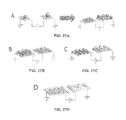
- FIG. 3A is an absorption cross section plot depicting ideal absorption spectra of uncoupled nanostructures.
- FIG. 3B is an absorption cross section plot depicting increases in the absorption spectrum for coupled nanostructures.
- FIG. 3C is an absorption cross section plot depicting shifts in the absorption maxima and an increase in the magnitude of absorption for coupled nanostructures.
- FIG. 4A is a device schematic of two electrically coupled metallic nanostructures having different structures according to an embodiment of the present invention.
- FIG. 4B is an absorption cross section plot depicting the plasmoelectric effect according to an embodiment of the present invention.
- FIG. 5A is a device schematic of two electrically coupled metallic nanostructures having different structures according to an embodiment of the present invention.
- FIG. 5B is a generally equivalent circuit for the device shown in FIG. 5A .
- FIG. 5C is a plot of the current-voltage response of the device of FIG. 5A .
- FIG. 6 depicts a thermodynamic analysis of possible device configurations according to embodiments of the present invention.
- FIG. 7 is a device schematic of two electrically coupled metallic nanostructures having different structures according to another embodiment of the present invention.
- FIG. 8 a is a device schematic of two electrically coupled metallic nanostructures having identical structures according to an embodiment of the present invention.
- FIG. 8 b is a generally equivalent circuit for the device of FIG. 8 a.
- FIG. 8 c is a plot of the current-voltage response of the device of FIG. 8 a.
- FIG. 9 is a polarization plot showing plasmon resonances for an Ag sphere at various radii and electron density values.
- FIG. 10A is an illustration of an electrochemical cell in which the particle surface charge density of an Au nanoparticle is tuned according to a voltage.
- FIG. 10B is a scattering intensity plot showing shifts in plasmon resonance with changes in voltage and charge density.
- FIG. 10C is a scattering plot showing the dependence of the plasmon resonance on charge density of the complex dielectric function of a plasmonic metal.
- the inset depicts a graph of wavelength relative to potential.
- FIG. 11A is an illustration of a thermodynamic model for a single plasmonic nanostructure perturbed from equilibrium by an incident radiation field.
- FIG. 11B is an illustration of a single plasmonic nanostructure subject to incident radiation.
- FIG. 11C is a plot showing the relationship between the ⁇ F potential (or electrochemical potential) and relative electron density for a spherical Ag nanoparticle.
- FIG. 12A is an entropy density plot depicting the thermoelectric effect.
- FIG. 12B is an entropy density plot depicting the plasmoelectric effect.
- FIG. 13 is an illustration of a thermodynamic model for a plasmoelectric device according to an embodiment of the present invention.
- the depicted plasmoelectric device is perturbed from equilibrium by an incident radiation field.
- EDDACS electron density-dependent absorption cross section
- FIG. 15A depicts an EDDACS for an individual 20 nm radius Ag sphere.
- FIG. 15B depicts an EDDACS for an individual 25 nm radius Ag sphere.
- FIG. 15C depicts a total EDDACS of a two-particle system including an electrically coupled pair of 20 nm and 25 nm radii Ag spheres.
- FIG. 15D is the same plot as FIG. 15C , minus the absorption of the system at a neutral charge configuration.
- FIG. 16A is an energy diagram for a 20 nm and 23 nm radii Ag particle couple irradiated at a wavelength of 485 nm.
- FIG. 16B depicts the change in absorption cross section of the Ag particle couple whose energy diagram is shown in FIG. 16A .
- FIG. 16C is a plot of the current-voltage response corresponding to the energy diagram of FIG. 16A .
- FIG. 17A shows a cross section plot and a scattering cross section plot for a 10 nm radius Ag sphere.
- FIG. 17B shows a cross section plot and a scattering plot for a 50 nm radius Au sphere.
- FIG. 17C shows an experimentally measured scattering intensity plot and a theoretical calculated scattering plot comparing white light scattering and monochromatic scattering.
- FIG. 18 a is a diagram of probing the absorption spectrum of a 60 nm diameter Au colloid in water with broadband or single frequency radiation by changing the sample position with respect to a grating monochrometer and white light source.
- FIG. 18 b is a plot of the absolute excitation of the 60 nm diameter Au colloid being probed in FIG. 18 a.
- FIG. 18 c is a plot of the absorption increase exhibited by the 60 nm diameter Au colloid being probed FIG. 18 a.
- FIG. 19A is a device schematic of a 10 nm radius Ag sphere irradiated with monochromatic light.
- FIG. 19B is a plot of the absorption maximum of the Ag sphere of FIG. 19A .
- FIG. 19C is a plot of the plasmoelectric potential of the Ag sphere of FIG. 19A under different incident intensities.
- FIG. 20A is an illustration of an electrochemical cell in which 100 nm diameter Au particles were adsorbed in a cellulose/polyester matrix until stained.
- FIG. 20B is an absorption cross section plot of the Au particles in FIG. 20A .
- FIG. 20C is a plot of the photovoltage of the electrochemical cell in FIG. 20A .
- FIG. 21A is an illustration of 60 nm diameter Au particles spincast on an indium tin oxide (ITO) film and compared with a bare ITO film in a 0.1 M NaCl/H 2 O electrolyte solution.
- ITO indium tin oxide
- FIG. 21B is an intensity plot showing the ensemble spectrum of the 60 nm diameter Au particles of FIG. 21A .
- FIG. 22A depicts a method of measuring induced plasmoelectric potential by Kelvin Probe Force Microscopy (KPFM).
- FIG. 22B is a KPFM surface map depicting three Au particles.
- FIG. 22C is an atomic force microscopy (AFM) image of a local sample region.
- AFM atomic force microscopy
- FIG. 23A depicts a method of measuring induced plasmoelectric potential by KPFM according to another approach.
- FIG. 23B is a plot of the absorption maximum of a 60 nm diameter Au nanoparticle on an ITO film.
- FIG. 23C is a plot of the theoretical plasmoelectric potential for the 60 nm diameter Au nanoparticle irradiated under an intensity of 10,000 W m ⁇ 2 .
- FIG. 23D is a plot of the experimental plasmoelectric potential for the 60 nm diameter Au nanoparticle irradiated with monochromatic light under an intensity of 10,000 W m ⁇ 2 .
- FIG. 23E is a voltage plot of a time study of the surface potential of an ITO substrate.
- FIG. 23F is a plot of the calculated absorption maximum of the Au nanoparticle.
- FIG. 24A is an AFM image of a local sample region.
- FIG. 24B is a plot of the measured potential of an Au particle.
- FIG. 25A is a plot of the measured potential of an Au particle as measured during a dark study compared with the measured potential of the particle irradiated at 514 nm during a light study under irradiation intensities of 1 mW and 10 mW.
- FIG. 25B is a plot of the measured potential of an Au particle as measured during a dark study compared with the measured potential of the particle irradiated at 514 nm during a light study under irradiation intensities of 10 mW and 200 mW.
- FIG. 26A is a KPFM surface potential map for 60 nm diameter Au particles irradiated at a wavelength of 532 nm in dark light.
- FIG. 26B is a KPFM surface potential map for 60 nm diameter Au particles irradiated at a wavelength of 532 nm under an irradiation intensity of 2 mW.
- FIG. 26C is a KPFM surface potential map for 60 nm diameter Au particles irradiated at a wavelength of 532 nm under an irradiation intensity of 30 mW.
- FIG. 26D is a KPFM surface potential map for 60 nm diameter Au particles irradiated at a wavelength of 532 nm under an irradiation intensity of 200 mW.
- FIG. 27A is a device schematic of a plasmoelectric device according to an embodiment of the present invention. To the right of the arrow is a plasmoelectric device in an array configuration according to another embodiment.
- FIG. 27B is a device schematic of a plasmoelectric device having a varied dielectric environment.
- FIG. 27C is a device schematic of a plasmoelectric device having a varied particle composition.
- FIG. 27D is a device schematic of a plasmoelectric device having other geometric parameters.
- Optically excited plasmonic nanostructures exhibit power density in the form of coherent oscillations of free electrons that ultimately decay as heat.
- the high internal energy density of optically excited plasmonic nanostructures results from the coupling of resonant free electron oscillations with incident radiation (e.g., incident light) at the structural resonance frequency.
- incident radiation e.g., incident light
- strong polarization occurs during irradiation of plasmonic nanostructures by laser excitation, which can induce fluctuations of ⁇ 10,000% or greater during each optical cycle.
- Resonant absorption induces electronic excitation that ultimately leads to significant internal heating (or highly localized heating).
- a steady-state temperature increase of 100 K occurs for resonant irradiation of 10 nm radius Ag spheres at a power density (or irradiation intensity) of 1 kW m ⁇ 2 .
- this source of power has not been efficiently harnessed to perform electrical work.
- plasmonic resonators that emit optically excited hot electrons across a rectifier (e.g., a semiconductor or insulator barrier) into a circuit have received attention as an energy generation mechanism, but have low efficiency.
- Embodiments of the present invention are directed to plasmoelectric devices for improved conversion efficiency of optical power to electrical power using resonant optical absorption in plasmonic nanostructures, and to methods of power conversion using resonant optical absorption in plasmonic nanostructures.
- nanostructures nanoparticles
- particles particles
- resonators are used interchangeably.
- the term “irradiate” is used to mean that an object is receiving or is exposed to irradiation.
- plasmonic resonance or “plasmon resonance” are used to refer to the wavelength or frequency value at which a nanostructure achieves maximum absorption.
- the symbol e ⁇ as shown in the drawings is used to denote the transfer of electrons and the transfer of charge generally.
- the nanostructure when a nanostructure is described as being “neutral,” the nanostructure may be in a state of equilibrium undisturbed by irradiation, or the nanostructure may be neutral during irradiation, if the incident radiation frequency is exactly resonant with the nanostructure.
- aspects of embodiments of the present invention provide an approach for generation of DC electrical power from resonant optical absorption in plasmonic nanostructures. This approach takes advantage of the plasmoelectric effect. Aspects of embodiments of the present invention also provide a physical model of the optical conditions and device structure used to convert optical power to DC electrical power in an all-conductor circuit. According to the plasmoelectric effect, power conversion results from the dependence of optically generated heat on shifts of the plasmon resonance frequency associated with changes of charge density. Rather than separation of electron-hole pairs, plasmoelectric power conversion exploits the dependence of the plasmon resonance frequency, ⁇ p , on electron density, n.
- a plasmoelectric device for conversion of optical power to DC electrical power includes first and second electrically coupled plasmonic nanostructures, each having a respective resonance value.
- the first plasmonic nanostructure is configured to receive irradiation at a first irradiation value and the second plasmonic nanostructure is configured to receive irradiation at a second irradiation value, to induce charge transfer between the first and second plasmonic nanostructures.
- FIG. 1 is a device schematic of a plasmoelectric device according to an embodiment of the present invention.
- the plasmoelectric device 10 includes a first plasmonic nanostructure 20 and a second plasmonic nanostructure 30 .
- the first and second plasmonic nanostructures 20 and 30 are electrically coupled via a first conduction element 40 .
- Incident light may originate from any optical source, such as the sun or a device that emits light (e.g., a laser).
- An optical structure 15 may be included in the plasmoelectric device 10 to direct, transmit or send irradiation to the first and second plasmonic nanostructures 20 and 30 .
- the optical structure 15 is configured to direct, transmit or send incident light 17 of various frequencies and wavelengths to the first and second plasmonic nanostructures 20 and 30 .
- the radiation profile incident on the plasmoelectric device 10 is optimized via one or more optical structures 15 , such that only the appropriate frequencies from the incident light source (e.g., the sun or a laser) are incident on the first and second plasmonic nanostructures 20 and 30 .
- the first plasmonic nanostructure 20 and the second plasmonic nanostructure 30 may be composed of plasmonic materials such as Ag or Au.
- the first plasmonic nanostructure 20 and the second plasmonic nanostructure 30 may have a nanoscale size.
- the first plasmonic nanostructure 20 and the second plasmonic nanostructure 30 are 10 nm radius Ag spheres.
- the present invention is not limited thereto, and objects of any suitable size or shape composed of plasmonic material may be used.
- the first plasmonic nanostructure 20 may have a different structure than the second plasmonic nanostructure 30 .
- the first plasmonic nanostructure 20 and the second plasmonic nanostructure 30 may be different sizes (e.g., spheres having different radii) or may be composed of different materials.
- the first plasmonic nanostructure 20 and the second plasmonic nanostructure 30 are surrounded by a dielectric material.
- the first plasmonic nanostructure 20 may be surrounded by a different dielectric material than the second plasmonic nanostructure 30 , or may be surrounded by the same dielectric material.
- Either one or both of the first plasmonic nanostructure 20 and the second plasmonic nanostructure 30 may be an array.
- Other embodiments of the first plasmonic nanostructure 20 and the second plasmonic nanostructure 30 are shown in FIGS. 27A through 27D .
- Conduction element 40 may be any element or component suitable for conducting charge, such as a wire.
- the plasmoelectric device 10 and circuitry 60 are electrically coupled via a second conduction element 50 (e.g., a wire).
- Circuitry 60 may be any circuit that uses DC electrical power to perform electrical work, and may include any number or combination(s) of electrical components such as resistors, capacitors, inductors, transistors, diodes, integrated circuit chips, and the like. Circuitry 60 may also be a circuit for storing the DC electrical power generated by the plasmoelectric device 10 .
- a plasmoelectric device for broadband power conversion includes a first array of electrically coupled plasmonic nanostructures, a second array of electrically coupled plasmonic nanostructures, and an optical structure configured to direct, transmit or send incident broadband radiation to each array.
- the first and second arrays are electrically coupled, and absorption maxima for the plasmonic nanostructures of the first and second arrays span an incident radiation spectrum.
- FIG. 2 depicts a plasmoelectric device 300 for broadband power conversion according to an embodiment of the present invention.
- the plasmoelectric device 300 includes identical first and second resonator arrays 310 and 320 .
- the first resonator array 310 includes electrically coupled plasmonic nanostructures 315 and the second resonator array 320 includes electrically coupled plasmonic nanostructures 325 .
- the absorption maxima for several neutral particle plasmonic nanostructures of each array span the incident radiation spectrum.
- FIG. 1 depicts a plasmoelectric device 300 for broadband power conversion according to an embodiment of the present invention.
- the plasmoelectric device 300 includes identical first and second resonator arrays 310 and 320 .
- the first resonator array 310 includes electrically coupled plasmonic nanostructures 315
- the second resonator array 320 includes electrically coupled plasmonic nanostructures 325 .
- the absorption maxima for several neutral particle plasmonic nanostructures of each array span the incident radiation spectrum
- the electrically coupled plasmonic nanostructures 315 of the first resonator array 310 have different radii or sizes from one another, and the electrically coupled plasmonic nanostructures 325 of the second resonator array 320 also have different radii or sizes from one another.
- An optical structure 305 directs, transmits, or sends incident broadband radiation from an optical light source 301 to the first resonator array 310 and the second resonator array 320 with a radiation profile optimized to maximize the plasmoelectric potential across the entire plasmoelectric device 300 .
- the optical structure 305 is an optical splitting element such as a diffractive filter.
- Each resonator in the array receives a band (e.g., a small band) of radiation that either induces a negative plasmoelectric potential or a positive plasmoelectric potential, to maximize the total voltage across the device.
- the plasmoelectric device 300 may be electrically coupled to any external circuitry 306 that utilizes DC electrical power or an electrical signal that is characteristic of the incident spectrum.
- a plasmoelectric device for broadband power conversion may include more than two arrays, and each array may include fewer or greater than four plasmonic nanostructures.
- the electrically coupled plasmonic nanostructures 315 and 325 may be composed of different plasmonic materials. Any number of different plasmonic nanostructures may be electrically coupled in an array so that absorption maxima for several of the neutral particle plasmonic nanostructures of the coupled arrays span the incident radiation spectrum.
- a method of converting optical power to DC electrical power includes providing electrically coupled first and second plasmonic nanostructures.
- the first plasmonic nanostructure has a first resonance value and the second plasmonic nanostructure has a second resonance value.
- the first and second plasmonic nanostructures receive irradiation to induce charge transfer between the first and second plasmonic nanostructures.
- the charge transfer produces a plasmoelectric potential and generates a current between the first and second plasmonic nanostructures.
- FIGS. 3A through 3C illustrate the spectral optimization of a plasmoelectric device for broadband power conversion according to an embodiment. Conversion efficiency may be maximized with the largest “usable” absorption bandwidth. Ideal absorption spectra of uncoupled nanostructures are shown in FIG. 3A . The uncoupled nanostructures exhibit several closely spaced overlapping peaks, except at the edge of the “usable” absorption bandwidth (indicated by the dashed lines). These spectral characteristics allow small transfers of electron density to cause large increases in the coupled absorption spectrum, which is shown in FIG. 3B . As shown in FIG. 3B , more, closer and sharper peaks improve efficiency.
- efficiency may be further enhanced if shifts in the absorption maxima are also accompanied by an increase in the magnitude of absorption, as in FIG. 3C .
- This may be achieved by adsorbing dyes on the nanostructures that absorb radiation only at the shifted peaks, for example.
- two electrically coupled plasmonic nanostructures 20 and 30 are provided, which have different structures so that they exhibit absorption maxima at distinct frequencies.
- the first plasmonic nanostructure 20 and the second plasmonic nanostructure 30 may be different sizes (e.g., spheres having different radii) or may be composed of different materials.
- the first plasmonic nanostructure 20 may be surrounded by a different dielectric material than the second plasmonic nanostructure 30 . Therefore, according to an embodiment the first resonance value of the first plasmonic nanostructure 20 is different from the second resonance value of the second plasmonic nanostructure 30 .
- the first plasmonic nanostructure 20 (having the first resonance value different from the second resonance value of the second plasmonic nanostructure 30 ) and the second plasmonic nanostructure 30 are both irradiated at an irradiation value between the first resonance value and the second resonance value.
- the irradiation promotes charge transfer from the higher frequency plasmonic nanostructure to the lower frequency plasmonic nanostructure.
- the charge transfer is from the first plasmonic nanostructure to the second plasmonic nanostructure.
- the first plasmonic nanostructure 210 is a 10 nm radius Ag sphere and the second plasmonic nanostructure 220 is a 20 nm radius Ag sphere.
- the first resonance value of the first plasmonic nanostructure 210 is at a higher frequency than the second resonance value of the second plasmonic nanostructure 220 .
- the first and second plasmonic nanostructures are electrically coupled via a conduction element 212 .
- the first plasmonic nanostructure 210 and the second plasmonic nanostructure 220 are exposed to or receive irradiation 211 with an irradiation value of 550 nm, which is between the first resonance value and the second resonance value, to induce charge transfer e ⁇ (or transfer of electrons) from the first plasmonic nanostructure 210 having a higher resonance frequency to the second plasmonic nanostructure 220 .
- the first plasmonic nanostructure 210 decreases in electron density and the second plasmonic nanostructure 220 increases in electron density. This produces a plasmoelectric potential difference between the first and second plasmonic nanostructures. A current is also generated due to the movement of charge from the first plasmonic nanostructure 210 to the second plasmonic nanostructure 220 .
- the charge transfer also causes a spectral shift as shown in FIG. 4B , such that the difference between the resonance values of the plasmonic nanostructures decreases (i.e., the plasmon resonances shift closer together).
- FIG. 5B is a generally equivalent circuit for the plasmoelectric device shown in FIGS. 4A and 5A .
- the plasmoelectric device 200 of FIG. 5A is represented as a voltage source 215 having an anode and a cathode (or a positive terminal and a negative terminal) connected in series with a current source 216 and an internal resistance R i .
- the plasmoelectric device 200 is represented as a voltage source 215 because of the plasmoelectric potential difference produced between the first and second nanostructures 210 and 220 as a result of the charge transfer.
- the plasmoelectric device 200 is represented as a current source 216 because the charge transfer through the conduction element 212 generates a current between the first and second nanostructures 210 and 220 .
- the internal resistance R i may represent the internal resistance of the conduction element 212 (such as a wire) between the first and second nanostructures 210 and 220 .
- the open circuit 214 may be electrically coupled to external circuitry 218 , which is depicted in FIG. 5B as a resistive load R load .
- FIG. 5C is a plot of the current-voltage response of the plasmoelectric device shown in FIGS. 4A and 5A .
- the first plasmonic nanostructure 20 (having the first resonance value different from the second resonance value of the second plasmonic nanostructure 30 ) and the second plasmonic nanostructure 30 are irradiated at an irradiation value other than the first and second resonance values.
- the first plasmonic nanostructure 20 may receive irradiation with a wavelength predominantly outside (or different from) the maximum absorption wavelengths for the neutral particles (e.g., outside a range defined by the first and second resonance values), and the second plasmonic nanostructure 30 may receive irradiation with a different wavelength that is also predominantly outside (or different from) the maximum absorption wavelengths for the neutral particles (e.g., outside a range defined by the first and second resonance values).
- the irradiation promotes charge transfer from the low frequency plasmonic nanostructure to the high frequency plasmonic nanostructure, in the opposite direction from the embodiment described above.
- FIG. 7 An example of this scenario is depicted in FIG. 7 .
- the geometry of the plasmonic device 140 is identical to the geometry of the plasmoelectric device 200 in FIG. 4A . That is, the first plasmonic nanostructure 150 is a 10 nm radius Ag sphere and the second plasmonic nanostructure 160 is a 20 nm radius Ag sphere. The first resonance value of the first plasmonic nanostructure 150 is at a higher frequency than the second resonance value of the second plasmonic nanostructure 160 .
- the first plasmonic nanostructure 150 and the second plasmonic nanostructure 160 are exposed to irradiation 111 with an irradiation value that is predominantly outside (or different from) the first and second resonance values, to induce charge transfer e ⁇ (or transfer of electrons) from the second plasmonic nanostructure 160 to the first plasmonic nanostructure 150 .
- the direction of movement of charge is in the opposite direction from the embodiment described above with respect to FIGS. 4A, 4B, and 5A-5C .
- the first plasmonic nanostructure 150 increases in electron density and the second plasmonic nanostructure 160 decreases in electron density. This produces a plasmoelectric potential difference between the first and second plasmonic nanostructures. A current is also generated due to the movement of charge from the second plasmonic nanostructure 160 to the first plasmonic nanostructure 150 .
- the charge transfer causes a spectral shift such that the difference between the plasmon resonance values of the plasmonic nanostructures increases (i.e., the plasmon resonances shift farther apart).
- two electrically coupled plasmonic nanostructures 20 and 30 are provided, which exhibit absorption maxima at approximately the same frequencies.
- the first resonance value of the first plasmonic nanostructure 20 is substantially equal to the second resonance value of the second plasmonic nanostructure 30 .
- the first plasmonic nanostructure 110 has an identical structure to the second plasmonic nanostructure 120 .
- the first plasmonic nanostructure 110 and the second plasmonic nanostructure 120 are both 10 nm radius Ag spheres. Therefore, the first resonance value of the first plasmonic nanostructure 110 is substantially equal to the second resonance value of the second plasmonic nanostructure 120 .
- the first plasmonic nanostructure receives irradiation 111 a with a first irradiation value of 550 nm and the second plasmonic nanostructure receives irradiation 111 b with a second irradiation value of 500 nm, to induce charge transfer (or transfer of electrons) from the first plasmonic nanostructure 110 to the second plasmonic nanostructure 120 .
- the first plasmonic nanostructure 210 decreases in electron density and the second plasmonic nanostructure 220 increases in electron density. This produces a plasmoelectric potential difference between the first and second plasmonic nanostructures. A current is also generated due to the movement of charge from the first plasmonic nanostructure 210 to the second plasmonic nanostructure 220 .
- the charge transfer also causes a spectral shift such that the first resonance value of the first plasmonic nanostructure 210 shifts to a longer wavelength and the second resonance value of the second plasmonic nanostructure 220 shifts to a shorter wavelength.
- FIG. 8 b is a generally equivalent circuit for the plasmoelectric device 100 shown in FIG. 8 a .
- the plasmoelectric device 100 of FIG. 8 a is represented as a voltage source connected in series with a current source and an internal resistance R i .
- FIG. 8 c is a plot of the current-voltage response of the plasmoelectric device of FIG. 8 a . According to an embodiment, as shown in FIG.
- plasmonic nanostructures with the same resonances may receive different incident radiation profiles, and plasmonic nanostructures with different resonances may receive incident radiation at the same frequency.
- charge transport between electrically coupled plasmonic nanostructures results from dependence of the plasmon resonance frequency of each nanostructure on its internal charge density.
- a power conversion device can improve the efficiency of power conversion from optical power to electrical power using an all-metal, or all-conductor, circuit.
- an all-conductor power conversion device includes a first plasmonic nanostructure having a first internal charge density and a second plasmonic nanostructure having a second internal charge density.
- the first and second plasmonic nanostructures are electrically coupled and are configured to receive irradiation to change the first and second internal charge densities.
- semiconductor or insulating components such as Schottky barriers or P-N junctions, are not required. However, in some embodiments, semiconductor or insulating components may be optionally included.
- the power conversion efficiency of a plasmoelectric power conversion device is not limited by the short excited-state lifetime of the internal electrons.
- FIG. 10A shows an electrochemical cell in which the particle surface charge density of a gold nanoparticle (AuNP) is tuned according to a voltage.
- the plasmon resonance frequency ⁇ p shifts with changes in voltage, and hence shifts with changes in charge density.
- the plasmon resonance shifts to longer wavelengths as the voltage is increased, and shifts to shorter wavelengths as the voltage is decreased.
- a decrease in electron density will “red-shift” a plasmon resonance to an increased wavelength (and thus a lower frequency), while an increase in electron density will “blue-shift” a plasmon resonance to a decreased wavelength (and thus a higher frequency).
- FIG. 10C is a scattering plot showing the dependence of the plasmon resonance on charge density of the complex dielectric function of a plasmonic metal. As shown in FIG. 10B , the shift in plasmon resonance is reversible under both signs of applied voltage.
- FIG. 11A shows a thermodynamic analysis of a nanostructure perturbed from equilibrium by an incident radiation field.
- the thermodynamic analysis provides a framework for understanding the plasmoelectric effect.
- F in represents the free energy available to the system from the incident radiation field;
- P abs represents the power absorbed by the nanostructure;
- U R represents the total internal energy of the nanostructure;
- TS R represents the internal heat, or entropy, of the nanostructure;
- F R represents the electrochemical free energy of the nanostructure;
- P emit represents the power re-emitted as thermal radiation; and
- F out represents the free energy that is converted into useful DC electrical work by the nanostructure.
- U R TS R +F R .
- increased absorption of incident radiation 501 by the nanostructure excites electrons 503 , which are converted into thermalized phonons, and increases the internal heat (entropy) TS R of the nanostructure.
- the internal heat TS R depends on the relative rates of optical absorption and thermalized re-emission 507 .
- the internal heat TS R is therefore a function of absorption C abs (n) by the nanostructure, the heat capacity of the nanostructure, and the electron-phonon coupling efficiency of the nanostructure.
- F total F in ⁇ U R +F R .
- the plasmoelectric effect may also be interpreted as a shift of the electrochemical potential or Fermi level, ⁇ F , of a plasmonic nanostructure under off-resonant radiation that is analogous to “doping” or “gating” of a semiconductor.
- the electrochemical free energy F R can therefore be expressed in terms of the change in electron density n, and defined in terms of the Fermi function as follows:
- FIG. 11C is a plot showing the relationship between the ⁇ F potential (or electrochemical potential) and the relative electron density (n/n Ag ) for a spherical Ag nanoparticle. According to FIG. 11C , the ⁇ F potential increases as relative electron density increases.
- FIG. 6 shows a thermodynamic analysis of three optically excited spherical Ag nanoparticles.
- the radiation profile and resonator geometry define the optical response of each sphere.
- Column (a) shows a 10 nm radius Ag sphere under 1 kW m ⁇ 2 excitation at a wavelength of 550 nm.
- Column (b) shows a 22 nm radius Ag sphere under 1 kW m ⁇ 2 excitation at a wavelength of 550 nm (the same irradiation as the sphere in column (a)).
- Column (c) shows a 10 nm radius Ag sphere under 1 kW m ⁇ 2 excitation at a wavelength of 500 nm.
- FIG. 6 shows the electrochemical free energy F R (black) associated with charge transfer plotted with the internal heat from absorption TS R (green or blue) for each nanostructure as a function of relative electron density (n/n Ag ).
- the bottom row of FIG. 6 shows the differential heat from absorption
- the induced potential depends on the frequency difference of the absorption peak and incident color (or the wavelength of the incident light).
- the total free energy of the nanostructure is at a minimum when:
- Equation 2 defines the electrochemical potential of the nanostructure induced by the plasmoelectric effect and the thermodynamically favored EDDACS C abs (n).
- thermodynamic analysis in FIG. 6 assumes that the electrochemical potential is primarily dependent on the free electron density of the metal as described by the Fermi function. This is generally true for all plasmonic resonators. However, surface effects, other properties of the metal band structure, or local electrostatic fields, for example, may also contribute to the electrochemical potential of a device depending on specific experimental implementations.
- an efficient device electrically couples nanostructures that maximize the total potential difference, such as the nanostructures shown in columns (a) and (b) of FIG. 6 or the nanostructures shown in columns (a) and (c) of FIG. 6 .
- plasmonic nanostructures with distinct absorption maxima are electrically coupled and irradiated at an irradiation value that is an intermediate frequency between the resonance frequencies.
- the irradiation value may be approximately an intermediate average of the plasmon resonance frequencies, but the irradiation value may also depend on the intensity of the incident radiation.
- Charge transfer is thermodynamically favored because of the increased heat from absorption that accompanies the consequent spectral shifts. The plasmoelectric effect therefore produces a thermodynamic potential driving charge transport between irradiated nanostructures.
- FIG. 4A shows a device schematic of two electrically coupled metallic nanostructures, each with a different plasmon resonance frequency ⁇ p .
- both nanostructures are irradiated at a frequency intermediate between the plasmon resonance frequency ⁇ p of each individual nanostructure, which induces electron transport from the high frequency nanostructure to the low frequency nanostructure.
- the device geometry shown in FIG. 4A does not require thermal gradients or semiconductor or insulator components, distinguishing it from other devices such as thermoelectric generators, rectennas, photovoltaics, or hot electron optical energy converters.
- FIG. 12A is a plot of the thermoelectric effect
- FIG. 12B is a plot of the plasmoelectric effect.
- FIGS. 12A and 12B draw a comparison between the thermoelectric effect and the plasmoelectric effect.
- the increase of entropy provided by temperature gradient (the blue area under the curve in FIG. 12A ) provides the driving force to move the electrons (from hot to cold) that generate the thermoelectric potential that can perform work.
- a plasmoelectric device can be understood as a type of heat engine.
- the quantity of optically generated heat depends on the absorbed power from the incident radiation field, such that the plasmoelectric potential favoring charge transfer reflects the EDDACS C abs (n) of each nanostructure.
- the magnitude of the potential corresponds to the increase of the internal temperature and heat (or entropy) generated by a change in charge density.
- the absorption cross section is an indication of the amount of radiation absorbed by a structure for a given optical power density. For example, solar radiation has a power density of approximately 1000 W m ⁇ 2 . If a structure has an absorption cross section of 1 m 2 , it will absorb 1000 W of power when placed in sunlight.
- ⁇ p * ( n ⁇ e 2 ⁇ o ⁇ m e * ) 1 / 2 ( 4 )
- e is the electron charge
- ⁇ o is the permittivity of free space
- m* e is the electron effective mass.
- FIG. 13 shows a system containing a plasmoelectric device according to an embodiment of the present invention.
- the plasmoelectric device is perturbed from equilibrium by an incident optical power density (or incident radiation) I ⁇ .
- this radiation is a Helmholtz free energy per unit volume available to the system, F in , that can perform work on the plasmoelectric device.
- the system can lower the total Helmholtz free energy by absorbing this free energy from the radiation field, raising the temperature and entropic heat, TS R , of the nanostructures.
- optical absorption mediates the conversion process, which corresponds to electron excitation followed by phonon thermalization.
- a spectral shift of the absorption maxima of the plasmoelectric device into resonance with the incident optical frequency provides a significant decrease of the free energy of the radiation field F in by increasing TS R .
- spectral shifts depend on a change of the electron density in each of the coupled resonators, as defined by C abs (n), and therefore increase the electrochemical free energy F R of the nanostructures compared to an equilibrium configuration of uncharged neutral Ag nanostructures.
- Equation 2 the device configuration that minimizes the total free energy of the system with respect to changes of the electron density n of each nanostructure occurs when Equation 2 is met.
- conservation of energy implies that all of the power absorbed by the plasmonic nanostructures, P abs , is either sent to a load, P load , or re-emitted as thermal radiation, P emit . This absorbed power depends on the product of the C abs (n) of the device and the incident radiation, I ⁇ .
- TS R is the equivalent internal entropy and temperature that an electrically neutral nanostructure with the same C abs (n) would exhibit under steady-state irradiation if no energy went to electrochemical work.
- An expression for TS R is provided below.
- a plasmoelectric device can increase entropy (and decrease free energy) with any charge configurations that increase the absorbed light energy TS R by more than the electrochemical work F R used to generate such an absorption cross section.
- the total free energy in the system depends on the fraction of incident radiation that is converted into the internal energy of the resonators and the fraction of that internal energy that is further converted into the electrochemical free energy associated with charge transfer.
- F total F in ⁇ U R +F R (8) Because the incident power has no dependence on the charge configuration of the nanostructures, the following expression describes the minimum free energy of the system with respect to changes of electron density:
- Equation 9 corresponds to a configuration of the nanostructures
- Equation 10 describes the thermodynamic favorability of charge transfer between nanostructures.
- the minimum free energy of the system corresponds to a configuration of charged, non-neutral particles.
- Equation 10 also defines the electrochemical potential of each nanostructure at the thermodynamically favored value of n. This condition is summarized for the calculated optical response of spherical Ag nanostructures in FIG. 6 , in the limit that no power is sent to a circuit load.
- the steady-state internal temperature and entropy of a nanostructure while it is irradiated at a single wavelength and intensity I ⁇ , for a specific C abs (n) can be determined according the analysis below. This analysis may be extended to larger incident bandwidths by accounting for the spectral power absorbed for some finite wavelength range.
- a two-temperature model describes the power flow between the conduction electrons, phonons, the circuit load, and the ambient environment during irradiation.
- the rate of energy exchange between electrons and phonons depends on the electron-phonon coupling constant, g, the respective lattice and electronic heat capacities, and , and the relative temperature difference.
- Equation 11 can be generalized to account for other energy pathways, such as the rate of heat loss through substrate diffusion, for example. Under steady-state conditions, these coupled equations give the following expression for the electron and phonon temperature of a resonator,
- T e I ⁇ ⁇ C abs ⁇ ( n ) - P load g + T l ( 13 )
- T l ( I ⁇ ⁇ C abs ⁇ ( n ) - P load + ⁇ ⁇ ⁇ A s ⁇ T ambient 4 ⁇ ⁇ ⁇ A s ) 1 / 4 ( 14 )
- a s is the surface area of the particle
- ⁇ 5.67 ⁇ 10 ⁇ 8 J s ⁇ 1 m ⁇ 2
- K ⁇ 4 is the Stefan-Boltzmann constant.
- the lattice heat capacity does not depend explicitly on electron density, so the phonon energy of the resonator depends on electron density only through the dependence of T l on the C abs (n) expressed in Equation 14.
- the internal electronic heat is a function of the electron density, n, and electronic temperature, T e , as described by the Sommerfeld model for the electronic heat capacity of metals.
- T e ⁇ S e m e ⁇ k B 2 ⁇ V ⁇ ⁇ ⁇ 2 / 3 h 2 ⁇ 3 2 / 3 ⁇ T e 2 ⁇ n 1 / 3 ( 16 )
- V is the particle volume
- m e is the electron rest mass
- ⁇ is the reduced Plank constant
- k B is the Boltzmann constant.
- FIG. 14 shows the change of the EDDACS C abs (n) according to Mie theory relative to the absorption cross section corresponding to the electron density n AG for a neutral Ag particle.
- increasing or decreasing electron density will generally increase absorption at shorter or longer incident wavelengths, respectively.
- Illumination with radiation spanning a large bandwidth of incident wavelengths above or below the neutral particle absorption peak, which is near 520 nm, will favor charge transfer to or from the particle, as predicted by the thermodynamic analysis presented above.
- FIG. 15A shows the EDDACS C abs (n) for an individual 20 nm radius Ag sphere and FIG. 15B shows the EDDACS C abs (n) for an individual 25 nm radius Ag sphere.
- each individual particle absorption peak blue-shifts with increasing electron density.
- FIG. 15C depicts the total absorption cross section of a two-particle system having the 20 nm radius Ag sphere and the 25 nm radius Ag sphere electrically coupled to one another. The total absorption cross section approaches a maximum near 485 nm, when the small sphere loses approximately 7% electron density and the large sphere gains approximately 7% electron density.
- FIG. 15D is the same plot as FIG. 15C , minus the absorption of the system at a neutral charge configuration.
- the system can increase entropy with charge configurations that increase the absorbed light energy more than the electrical work used to generate those configurations.
- a device with high conversion efficiency will maximize the bandwidth and minimize the work associated with the lower red region of the plot in FIG. 15D .
- excitation at frequencies in the upper red region will reverse the polarity of the device.
- FIG. 16A is an energy diagram for a 20 nm and 23 nm radii Ag particle couple irradiated at a wavelength of 485 nm.
- FIG. 16B shows the change in absorption cross section of the Ag particle couple.
- the green curve represents the electrochemical work used to generate such an absorption cross section.
- the red curve represents the change in absorbed energy, ⁇ *I ⁇ .
- the product ⁇ *I ⁇ defines the steady-state energy available to the electrons when multiplied by the absorption cross section.
- the increase in absorbed energy (red) should be larger than the work (green).
- FIG. 16C is a plot of the current-voltage response corresponding to the energy diagram of FIG. 16A .
- FIGS. 14 through 16C suggests several different power conversion strategies via the plasmoelectric effect.
- the constraint is imposed that the nanostructures are isothermally coupled so that there is no additional thermoelectric potential across the device due to a thermal gradient between the nanostructures.
- two electrically coupled nanostructures have different structures, e.g. particle radii, or surrounded by a different dielectric matrix, so that they exhibit absorption maxima at distinct frequencies.
- the nanostructures are chosen so that the upper left (red) quadrant of a C abs (n) plot like that in FIG. 14 , describing the low frequency nanostructure, overlaps in the same wavelength range as the lower right quadrant of the similar plot describing the high frequency nanostructure.
- Incident radiation with wavelengths contained in the overlap region promotes charge transfer from the high frequency nanostructure to the low frequency nanostructure, and the absorption maxima of both shift towards a frequency in the overlap region. This same scenario is depicted in FIG. 4B .
- two electrically coupled nanostructures having the same device geometry as described above are irradiated at wavelengths predominantly outside (or different from) the maximum absorption wavelength for the neutral particles.
- two nanostructures with identical plasmon resonant absorption maxima but irradiated at different wavelengths can be electrically coupled.
- FIG. 8 a shows a device schematic of a plasmoelectric device according to an embodiment of the present invention.
- a plasmoelectric device 100 includes two electrically coupled metallic nanostructures 110 and 120 .
- One nanostructure is irradiated at a wavelength of 550 nm while the other nanostructure is irradiated at a wavelength of 500 nm.
- Equation 10 determines the efficiency with which the absorbed power can be sent to an external load. Since the free energy of the resonators must be extracted at a rate consistent with the power conservation law expressed in Equation 5, Equations 10 and 5 can be solved for a completed description of the current response of the device connection to a circuit load. Equation 10 is first expressed in terms of the Fermi level, ⁇ p , of an electron gas
- the magnitude of the plasmoelectric potential depends on the power lost to the load through Equations 13 and 14, but this potential also defines the power lost to the load through Equations 20 and 21.
- V load depends on I load through the temperature dependence of Equation 17, but V load also defines I load through Equation 18.
- Equation 5 The power absorbed by the plasmonic nanostructures is expressed in Equation 5.
- P abs ( n ) ⁇ P abs ( n AG ) P emit ( n ) ⁇ P emit ( n AG )+ P load ( n ) (23)
- thermodynamically favored ⁇ tot and resulting current through the load I load when P load takes the limiting minimum value of zero, corresponding to open circuit, through the maximum possible value, P load P abs (n) ⁇ P abs (n AG ), corresponding to short circuit.
- the solved current and voltage values for this range of P load are displayed in FIG. 8 c .
- the plotted value of the open circuit voltage V OC is approximately 50 mV lower than the estimated value of ⁇ tot ⁇ 500 mV. This difference reflects the constraint that both nanostructures are isothermally coupled as modeled, and that as a pair, they adopt the average temperature of the nanostructures displayed in columns (a) and (c) of FIG. 6 .
- the optical power conversion efficiency may be calculated by dividing the value of P load at each value of V load by the absorbed power from the radiation field P abs (n) when the EDDACS C abs (n) adopts the value of n corresponding to that potential.
- the highest conversion efficiency for the device may not correspond to operation at the maximum power point of the current-voltage response, because the absorbed power depends strongly on the potential adopted by the nanostructures.
- FIG. 5A shows a device schematic of a plasmoelectric device according to another embodiment of the present invention.
- a plasmoelectric device 200 includes two electrically coupled metallic nanostructures 210 and 220 , each with a different plasmon resonance frequency ⁇ p . Both nanostructures 210 and 220 are irradiated at a frequency intermediate between the plasmon resonance frequency ⁇ p of each individual nanostructure, which induces electron transport from the high frequency nanostructure to the low frequency nanostructure.
- the plasmonic nanostructure 210 is a 10 nm radius Ag sphere irradiated at a wavelength of 550 nm and the plasmonic nanostructure 220 is a 20 nm radius Ag sphere irradiated at a wavelength of 550 nm.
- FIG. 5B is the equivalent circuit of the plasmoelectric device shown in FIG. 5A .
- the total electrostatic potential, ⁇ tot equals the difference between the potentials on each individual nanostructure when isothermally coupled.
- ⁇ tot ( ⁇ F ) A ⁇ ( ⁇ F ) B (24) Equations 17 through 23 may be used to analyze the current-voltage response of the device geometry shown in FIG. 5A .
- FIG. 5C is a current-voltage plot showing the power curve of the circuit in FIG. 5B .
- thermodynamic analysis may be extended to device geometries optimized for broadband optical power conversion.
- aspects of embodiments of the present invention relate to strategies for maximizing conversion efficiency in broadband devices that take advantage of the spectral tunability of plasmonic nanostructures. Such devices may allow for more efficient broadband conversion of the entire solar spectrum.
- FIG. 2 depicts a plasmoelectric device 300 for broadband power conversion according to an embodiment of the present invention.
- the peaks of the absorption maxima of the nanostructures in the arrays should be as sharp as possible (i.e., each absorption maxima has a small line width).
- the term “line width” refers to the wavelength spread of an absorption peak at half of its maximum intensity (or “full width at half maximum,” FWHM).
- FWHM full width at half maximum
- thermodynamic power conversion efficiency for such an arrangement is constrained by Carnot analysis.
- an optimized broadband power conversion device can theoretically convert optical power at an efficiency that is only constrained by the fundamental thermodynamic limitation of an ideal heat engine, as described by Carnot analysis.
- the theoretical maximum efficiency ⁇ max of any heat engine may be defined in terms of the temperatures it operates between:
- T h the absolute temperature of the hot source
- T c the absolute temperature of the cold sink
- a plasmoelectric device for broadband conversion approaches the limiting Carnot efficiency of >90%, thereby rivaling the theoretical power conversion efficiency of conventional photovoltaic and thermoelectric devices.
- the relevant temperature difference for the Carnot analysis corresponds to the steady-state temperature of the nanostructure array at the thermodynamically favored value of electron density versus the corresponding electron density for a neutral particle in a dark ambient.
- FIGS. 17A and 17B demonstrate the apparent broadening of scattering spectra under monochromatic excitation due to the frequency-dependent change of charge density.
- the cross section plot on the left of FIG. 17A depicts an absorption curve (solid line) and a scattering curve (dotted line) of a 10 nm radius Ag sphere irradiated with white light. As shown in the cross section plot, the absorption curve and scattering curve overlap in frequency and exhibit a sharp peak at the plasmon resonance wavelength.
- 17A depicts absorption curves (solid line) and a scattering curve (dotted line) of the 10 nm radius Ag sphere irradiated with a monochromatic scan under incident intensities of 1000 W m ⁇ 2 and 100 W m ⁇ 2 .
- the absorption and scattering curves exhibit pronounced, symmetric broadening when irradiated with the monochromatic scan.
- the cross section plot on the left of FIG. 17B depicts an absorption curve (solid line) and a scattering curve (dotted line) of a 50 nm radius Au sphere irradiated with white light.
- the absorption curve and the scattering curve are broader than in the cross section plot of FIG. 17A .
- the scattering curve is red-shifted relative to the absorption curve.
- the scattering plot on the right of FIG. 17B depicts absorption curves (solid line) and a scattering curve (dotted line) of the 50 nm radius Au sphere irradiated with a monochromatic scan under incident intensities of 1,000,000 W m ⁇ 2 , 10,000 W m ⁇ 2 and 1000 W m ⁇ 2 .
- the absorption and scattering curves exhibit asymmetric broadening of the scattering signal.
- FIG. 17C shows an experimental scattered intensity plot (left) and theoretical scattering plot (right) comparing white light scattering (gray and black traces) and monochromatic scattering (green trace). In the theoretical scattering plot on the right, only a red-shift is observed from monochromatic scattering. In the experimental scattered intensity plot on the left, the gray and black traces show the white light curve before and after the monochromatic scan. The overlap of the gray and black traces shows that the plasmoelectric response is reversible.
- the green trace shows more scattering from 560 nm-640 nm compared with the gray and black traces (i.e., the white light curves), indicating that a plasmoelectric potential was induced by the monochromatic light.
- the comparison of the white light spectra with the monochromatic spectra confirms the plasmoelectric effect.
- FIG. 18 a is a diagram of probing the absorption spectrum of a 60 nm diameter Au colloid in water with broadband or single frequency radiation by changing the sample position with respect to a grating monochrometer and white light source.
- FIG. 18 b is a plot of the absolute excitation of the 60 nm diameter Au colloid being probed in FIG. 18 a .
- Samples probed monochromatically (red trace) exhibited systematic increases of absorption compared to the spectrum obtained during broadband illumination (black trace).
- FIG. 18 c is a plot of the absorption increase exhibited by the 60 nm diameter Au colloid being probed FIG. 18 a .
- the power- and frequency-dependent increases of absorption indicate an optically induced change of charge density consistent with the predicted plasmoelectric response for this system.
- the spectral and intensity dependence of the plasmoelectric potential may also be observed by electrical measurement as shown in FIG. 19A .
- FIG. 19A a 10 nm radius Ag sphere is irradiated with monochromatic light at a wavelength of 550 nm, and the induced potential is measured.
- FIG. 19B is a plot of the absorption maximum of the Ag sphere.
- FIG. 19C depicts the plasmoelectric potential under incident intensities of 1000 W m ⁇ 2 , 500 W m ⁇ 2 , and 100 W m ⁇ 2 .
- the magnitude of the plasmoelectric potential depends on the intensity of the incident radiation.
- the sign of the plasmoelectric potential depends on the frequency: incident blue light at shorter wavelengths produces a negative potential and incident red light at longer wavelengths produces a positive potential.
- FIG. 20A is an electrochemical cell in which 100 nm diameter Au particles were adsorbed in a cellulose/polyester matrix until stained (right vial).
- the absorption cross section of the Au particles is shown in FIG. 20B .
- the Au particles in 0.5 M NaCl solution were irradiated using a scanned monochromatic light source and the measured photovoltage of the electrolyte solution was compared with a control sample (left vial) as a function of wavelength. Comparing the photovoltage plot of FIG. 20C with the absorption cross section of FIG. 20B , a sign change can be observed near the absorption maximum of the particles in the solution, at approximately 560 nm.
- FIG. 21A depicts another method of measuring the photovoltage of nanoparticles using an adaptation of the geometry of Dondapati, S. K., Ludemann, M., Mueller, R., Schwieger, S., Schwemer, A., Haendel, B., Kwiatkowski, D., et al., Voltage-Induced Adsorbate Damping of Single Gold Nanorod Plasmons in Aqueous Solution, Nano Letters, 12(3), 1247-1252. doi:10.1021/n1203673g (2012), the entire content of which is incorporated herein by reference.
- FIG. 21A depicts another method of measuring the photovoltage of nanoparticles using an adaptation of the geometry of Dondapati, S. K., Ludemann, M., Mueller, R., Schwieger, S., Schwemer, A., Haendel, B., Kwiatkowski, D., et al., Voltage-Induced Adsorbate Damping of Single Gold Nanorod Plasmons in Aque
- FIG. 21A 60 nm diameter Au particles are spincast on ITO film and compared with a bare ITO film in a 0.1 M NaCl/H 2 O electrolyte solution.
- FIG. 21B is an intensity plot showing the ensemble spectrum of 60 nm diameter Au particles on ITO. When the solution is irradiated at a wavelength of 515 nm, a photovoltage of ⁇ 3 mV is observed, and when the solution is irradiated at a wavelength of 630 nm, a photovoltage of +1 mV is observed.
- the sign of the measured photovoltage is consisted with the predicted behavior of the plasmoelectric effect, in which incident blue light at shorter wavelengths produces a negative potential and incident red light at longer wavelengths produces a positive potential.
- the low magnitude of the observed photovoltage is likely due to the very low optical density of the sample and the in-series resistance of the sample geometry.
- the induced plasmoelectric potential may also be measured using KPFM, an AFM technique.
- KPFM uses a scanning probe to measure the work function difference between a conductive tip of the probe and a sample.
- the sample shown in FIG. 22A contains a 60 nm average diameter Au colloid on an ITO film.
- a generated nanoscale map of the surface potential is generated which shows the work function offset compared with the sample.
- the KPFM surface map in FIG. 22B depicts three Au particles and shows the work function offset compared with the ITO film.
- FIG. 22C is an AFM image of a local sample region.
- FIG. 23A shows an example of using KPFM to directly probe the plasmoelectric potential of a nanoparticle.
- the area containing a particle to be irradiated with light is separated from the KPFM conductive tip so that the surface potential of the ITO film is measured while the tip is kept dark.
- FIG. 23B is a plot of the absorption maximum of the particle, which is a 60 nm diameter Au nanoparticle on an ITO film.
- FIG. 23C is a plot of the theoretical plasmoelectric potential for the Au nanoparticle irradiated under an intensity of 10,000 W m ⁇ 2 .
- 23D is a plot of the experimental plasmoelectric potential for the Au nanoparticle irradiated with monochromatic light under an intensity of approximately 10,000 W m ⁇ 2 .
- the induced potential of a single particle changes sign with light on either side of the absorption maximum of FIG. 23B .
- FIGS. 23C and 23D there is a clear shift of surface potential while scanning with monochromatic light. The observed sign change is consistent with the plasmoelectric effect.
- FIG. 23E is a voltage plot of a time study of the surface potential of an ITO substrate.
- the conductive tip of the scanning probe is kept dark to avoid heating and photocarrier generation in the tip.
- the voltage plot shows a clear shift of the surface potential with changes in the incident color, from positive at an incident wavelength of 532 nm (red light) to negative at an incident wavelength of 496 nm (blue light). This sign change is consistent with the plasmoelectric effect.
- the calculated absorption maximum is shown in the plot of FIG. 23F .
- FIGS. 24A and 24B depict the results of a dark study conducted near 60 nm diameter Au particles.
- FIG. 24A is an AFM image of a local sample region.
- FIG. 24B is a plot of the measured potential of the Au particles.
- the potential on the ITO is defined as zero and KPFM line scans over the Au particles (blue) resolve their potential offset with ITO.
- the dark study shows that the KPFM technique has resolution that can resolve the individual particles (i.e., the surface potential contrast between Au particles and ITO is resolved).
- FIGS. 25A and 25B depict the results of a light study conducted near a 60 nm diameter Au particle under incident radiation at a wavelength of 514 nm.
- the incident radiation profile including the incident wavelength and the light intensity, affects the optimal particle size.
- a nanoparticle has an optimal size when it has resonance that is closer to the incident wavelength, based on variations in size. It is predicted that the plasmoelectric voltage will have a negative polarity and will scale with the light intensity.
- FIGS. 25A and 25B are plots of the measured potential of the particle as measured during the dark study (“Dark”) compared with the measured potential of the particle irradiated at 514 nm during the light study under irradiation intensities of 1 mW, 10 mW, and 200 mW. With high light intensity, the entire surface region potential is lowered. For example, under an incident light intensity of 200 mW, the entire surface region potential is lowered by 170 mV as compared with the surface region potential under an incident light intensity of 10
- FIGS. 26A through 26D present a full view of samples corresponding to line scans of a plasmoelectric device such as that shown in FIG. 2 .
- FIG. 26A is a KPFM surface potential map for 60 nm diameter Au particles irradiated at a wavelength of 532 nm in dark light.
- FIGS. 26B through 26D are KPFM surface potential maps for 60 nm diameter Au particles irradiated at a wavelength of 532 nm under irradiation intensities of 2 mW, 30 mW and 200 mW, respectively.
- FIGS. 27A through 27D depict several alternative device schemes that may be employed.
- FIG. 27A shows a plasmoelectric device according to an embodiment on the left hand side, which assumes no optical coupling between separated spheres (e.g., no bonding or anti-bonding optical modes).
- the device could be an array.
- plasmoelectric devices according to embodiments of the present invention could vary the dielectric environment as shown in FIG. 27B , the particle composition as shown in FIG. 27C , or other geometric parameters as shown in FIG. 27D .
- the plasmoelectric effect may be employed for optical power conversion or wireless power transfer as described herein, the phenomenon may also be used in other applications such as developing a new class of optoelectronic devices.
- the plasmoelectric effect may modulate the absorption cross section at specific frequencies for applications relating to optical switching.
- a plasmoelectric device for broadband power conversion like that in FIG. 2 could produce an electrical signal that is characteristic of the incident spectrum, enabling subwavelength spectrometers with electronic readout.
- the plasmoelectric effect permits active control of the Fermi level of a metal using incident radiation.
- new types of all-metal optoelectronic devices may be developed by replacing the usual function of doped or gated semiconductor components with metal nanostructures that are optically excited off-resonance, an approach that is facilitated by the spectral tailorability of plasmonic nanostructures.
Landscapes
- Chemical & Material Sciences (AREA)
- Engineering & Computer Science (AREA)
- Nanotechnology (AREA)
- Physics & Mathematics (AREA)
- Composite Materials (AREA)
- Condensed Matter Physics & Semiconductors (AREA)
- General Physics & Mathematics (AREA)
- Materials Engineering (AREA)
- Crystallography & Structural Chemistry (AREA)
- Chemical Kinetics & Catalysis (AREA)
- Optical Modulation, Optical Deflection, Nonlinear Optics, Optical Demodulation, Optical Logic Elements (AREA)
Abstract
Description
(green or blue), plotted with the differential free energy,
(black), where
The induced potential depends on the frequency difference of the absorption peak and incident color (or the wavelength of the incident light).
ω*p ∝n 1/2 (3)
where e is the electron charge, εo is the permittivity of free space, and m*e is the electron effective mass. This strategy is consistent with other work that examined carrier density-dependent plasmon shifts, for example in doped semiconductors, electrochemical cells, or at metal surfaces during ultrafast pump-probe measurements.
P abs =I λ ·C abs(n)=P emit +P load (5)
The specific Cabs(n) the device adopts in steady-state defines the total internal energy UR, heat TSR, and free energy FR of the nanostructures. These relations are derived explicitly below, and reflect the internal temperature and charge density associated with a given configuration. For changes of electron density,
Here,
F total =F in −U R +F R (8)
Because the incident power has no dependence on the charge configuration of the nanostructures, the following expression describes the minimum free energy of the system with respect to changes of electron density:
Substitution of
where As is the surface area of the particle, ε is the emissivity (ε=1 for a perfect black body) and σ=5.67×10⁻⁸ J s−1 m−2 K−4 is the Stefan-Boltzmann constant.
Here, V is the particle volume, me is the electron rest mass, ℏ is the reduced Plank constant, and kB is the Boltzmann constant. Increases of electronic temperature efficiently compensate for entropy losses associated with decreased electron density in a plasmoelectric device.
where ΔεF=εF(n)−εF(nAg) is given by the Fermi function:
The value of n that satisfies
ϕtot=(ΔεF)A−(ΔεF)C (19)
Any temperature gradient between nanostructures would produce an additional thermoelectric potential. Based on columns (a) and (c) of
V load=ϕtot (20)
The power through the load (or the power lost to the circuit load), Pload, relates to this voltage drop Vload and the magnitude of the current through the load, Iload according to Ohm's law:
P load =V load ·I load (21)
As such, the magnitude of the plasmoelectric potential depends on the power lost to the load through Equations 13 and 14, but this potential also defines the power lost to the load through
P abs(n AG)=I λ ·C abs(n AG)=P emit(n AG) (22)
This equation is subtracted from both sides of
P abs(n)−P abs(n AG)=P emit(n)−P emit(n AG)+P load(n) (23)
ϕtot=(ΔεF)A−(ΔεF)B (24)
where Th is the absolute temperature of the hot source and Tc is the absolute temperature of the cold sink.
Claims (16)
Priority Applications (1)
| Application Number | Priority Date | Filing Date | Title |
|---|---|---|---|
| US13/679,995 US10075104B2 (en) | 2011-11-16 | 2012-11-16 | Plasmonic nanostructures for conversion of optical power to electrical power |
Applications Claiming Priority (3)
| Application Number | Priority Date | Filing Date | Title |
|---|---|---|---|
| US201161560703P | 2011-11-16 | 2011-11-16 | |
| US201261583507P | 2012-01-05 | 2012-01-05 | |
| US13/679,995 US10075104B2 (en) | 2011-11-16 | 2012-11-16 | Plasmonic nanostructures for conversion of optical power to electrical power |
Publications (2)
| Publication Number | Publication Date |
|---|---|
| US20130133711A1 US20130133711A1 (en) | 2013-05-30 |
| US10075104B2 true US10075104B2 (en) | 2018-09-11 |
Family
ID=48465704
Family Applications (1)
| Application Number | Title | Priority Date | Filing Date |
|---|---|---|---|
| US13/679,995 Active 2034-08-22 US10075104B2 (en) | 2011-11-16 | 2012-11-16 | Plasmonic nanostructures for conversion of optical power to electrical power |
Country Status (1)
| Country | Link |
|---|---|
| US (1) | US10075104B2 (en) |
Cited By (1)
| Publication number | Priority date | Publication date | Assignee | Title |
|---|---|---|---|---|
| US11283304B2 (en) * | 2017-12-04 | 2022-03-22 | Universite D'aix-Marseille | Plasmonic rectenna device and method of manufacturing |
Families Citing this family (2)
| Publication number | Priority date | Publication date | Assignee | Title |
|---|---|---|---|---|
| WO2018049052A1 (en) * | 2016-09-07 | 2018-03-15 | The Regents Of The University Of California | System and method for using exceptional points in plasmonic nanostructures for sensing, communication and imaging |
| CN110421263B (en) * | 2019-07-09 | 2021-01-22 | 湖南工业大学 | Fine correction method for face gear |
Citations (4)
| Publication number | Priority date | Publication date | Assignee | Title |
|---|---|---|---|---|
| US4482778A (en) * | 1983-04-19 | 1984-11-13 | The United States Of America As Represented By The Administrator Of The National Aeronautics And Space Administration | Solar energy converter using surface plasma waves |
| US20080291453A1 (en) * | 2004-06-17 | 2008-11-27 | Kyushu University, National University Corporation | Surface Plasmon Resonance Phenomenon Measuring Equipment |
| US20090091762A1 (en) * | 2007-09-03 | 2009-04-09 | Rohm Co., Ltd. | Metallic structure and photodetector |
| WO2011056501A1 (en) * | 2009-11-06 | 2011-05-12 | The Trustees Of The University Of Pennsylvania | Optoelectronic devices employing plasmon induced currents |
-
2012
- 2012-11-16 US US13/679,995 patent/US10075104B2/en active Active
Patent Citations (5)
| Publication number | Priority date | Publication date | Assignee | Title |
|---|---|---|---|---|
| US4482778A (en) * | 1983-04-19 | 1984-11-13 | The United States Of America As Represented By The Administrator Of The National Aeronautics And Space Administration | Solar energy converter using surface plasma waves |
| US20080291453A1 (en) * | 2004-06-17 | 2008-11-27 | Kyushu University, National University Corporation | Surface Plasmon Resonance Phenomenon Measuring Equipment |
| US20090091762A1 (en) * | 2007-09-03 | 2009-04-09 | Rohm Co., Ltd. | Metallic structure and photodetector |
| WO2011056501A1 (en) * | 2009-11-06 | 2011-05-12 | The Trustees Of The University Of Pennsylvania | Optoelectronic devices employing plasmon induced currents |
| US20120280209A1 (en) * | 2009-11-06 | 2012-11-08 | The Trustees Of The University Of Pennsylvania | Optoelectronic devices employing plasmon induced currents |
Non-Patent Citations (23)
| Title |
|---|
| Atay, et al., Nano Letters, 2004, vol. 4, No. 9, pp. 1627-1631. * |
| Atwater, H. A., et al., "Plasmonics for Improved Photovoltaic Devices", Nature Materials, vol. 9, Mar. 2010, pp. 205-213 and Corrigendum. |
| Blatt, Frank J., et al., Thermoelectric Power of Metals, Plenum Press,1976, pp. 1-47, Plenum, New York, 48 pages. |
| Dondapati, S. K., et al., "Voltage-Induced Adsorbate Damping of Single Gold Nanorod Plasmons in Aqueous Solution", Nano Letters, 2012, vol. 12, pp. 1247-1252. |
| Garcia, G., et al., "Dynamically Modulating the Surface Plasmon Resonance of Doped Semiconductor Nanocrystals", Nano Letters, 2011, vol. 11, pp. 4415-4420. |
| Gordon, J. G., II, et al., "Surface Plasmons as a Probe of the Electrochemical Interface", Surface Science 101, 1980, pp. 499-506. |
| Jain, P. K., et al., "Noble Metals on the Nanoscale: Optical and Photothermal Properties and Some Applications in Imaging, Sensing, Biology, and Medicine", Accounts of Chemical Research, Dec. 2008, vol. 41, No. 12, pp. 1578-1586. |
| Knight, M. W., et al., "Photodetection with Active Optical Antennas", Science, May 2011, vol. 332, pp. 702-704. |
| Luther, J. M., et al., "Localized Surface Plasmon Resonances Arising from Free Carriers in Doped Quantum Dots", Nature Materials, vol. 10, May 2011, pp. 361-366. |
| MacDonald, K. F., et al., "Ultrafast Active Plasmonics", Nature Photonics, vol. 3, Jan. 2009, pp. 55-58. |
| Maier, S. A., et al., "Plasmonics-A Route to Nanoscale Optical Devices", Advanced Materials, 2001, vol. 13, pp. 1501-1505. |
| Maier, S. A., et al., "Plasmonics—A Route to Nanoscale Optical Devices", Advanced Materials, 2001, vol. 13, pp. 1501-1505. |
| Maier, Stefan A., Plasmonics: Fundamentals and Applications, Springer Science Business Media LLC, 2007, pp. 1-19, New York, 17 pages. |
| Marty, R., et al., "Charge Distribution Induced Inside Complex Plasmonic Nanoparticles", Optics Express, Feb. 2010, vol. 18, No. 3, pp. 3035-3044. |
| Nelson, Jenny, The Physics of Solar Cells, Imperial College Press, 2003, pp. 1-87, World Scientific Publishing Co. Pte. Ltd., Singapore, 46 pages. |
| Odom, T. W., et al., "Introduction to Plasmonics", Chemical Reviews, 2011, vol. 111, pp. 3667-3668. |
| Pillai, S., et al., "Surface Plasmon Enhanced Silicon Solar Cells", Journal of Applied Physics, vol. 101, 2007, pp. 093105:1-8. |
| Polman, A., "Plasmonics Applied", Science, Nov. 2008, vol. 322, pp. 868-869. |
| Rakic, A. D., et al., "Optical Properties of Metallic Films for Vertical-Cavity Optoelectronic Devices", Applied Optics, Aug. 1998, vol. 37, No. 22, pp. 5271-5283. |
| Reinhard, B. M., et al., "Use of Plasmon Coupling to Reveal the Dynamics of DNA Bending and Cleavage by Single EcoRV Restriction Enzymes", PNAS, Feb. 2007, vol. 104, No. 8, pp. 2667-2672. |
| Sheldon, M. T., et al., "The Plasmoelectric Effect: Optically Induced Electrochemical Potentials in Resonant Metallic Structures", Thomas J. Watson Laboratories of Applied Physics, California Institute of Technology, Pasadena, CA; Date Unknown, pp. 1-24. |
| Wang, F., et al., "Power-Independent Wavelength Determination by Hot Carrier Collection in Metal-Insulator-Metal Devices", Nature Communications, Apr. 2013, pp. 1-7. |
| Yu, W. J., et al., "Small Hysteresis Nanocarbon-Based Integrated Circuits on Flexible and Transparent Plastic Substrate", Nano Letters, 2011, vol. 11, pp. 1344-1350. |
Cited By (1)
| Publication number | Priority date | Publication date | Assignee | Title |
|---|---|---|---|---|
| US11283304B2 (en) * | 2017-12-04 | 2022-03-22 | Universite D'aix-Marseille | Plasmonic rectenna device and method of manufacturing |
Also Published As
| Publication number | Publication date |
|---|---|
| US20130133711A1 (en) | 2013-05-30 |
Similar Documents
| Publication | Publication Date | Title |
|---|---|---|
| Zhu et al. | Engineering plasmonic hot carrier dynamics toward efficient photodetection | |
| Tielrooij et al. | Hot-carrier photocurrent effects at graphene–metal interfaces | |
| Lombardi | The theory of surface-enhanced Raman scattering on semiconductor nanoparticles; toward the optimization of SERS sensors | |
| Fast et al. | Hot-carrier optoelectronic devices based on semiconductor nanowires | |
| Bright et al. | Performance of near-field thermophotovoltaic cells enhanced with a backside reflector | |
| Seletskiy et al. | Laser cooling in solids: advances and prospects | |
| Song et al. | Energy flows in graphene: hot carrier dynamics and cooling | |
| Mlinar | Engineered nanomaterials for solar energy conversion | |
| Niu et al. | Ultrabroadband, fast, and flexible photodetector based on HfTe5 crystal | |
| Binks | Multiple exciton generation in nanocrystal quantum dots–controversy, current status and future prospects | |
| Yang et al. | Performance analysis of a near-field thermophotovoltaic device with a metallodielectric selective emitter and electrical contacts for the photovoltaic cell | |
| Pandya et al. | Exciton–phonon interactions govern charge-transfer-state dynamics in CdSe/CdTe two-dimensional colloidal heterostructures | |
| Joyce et al. | The influence of surfaces on the transient terahertz conductivity and electron mobility of GaAs nanowires | |
| Zhang et al. | Ultrasensitive and self‐powered terahertz detection driven by nodal‐line dirac fermions and Van der Waals architecture | |
| Yanover et al. | Significance of small-sized PbSe/PbS core/shell colloidal quantum dots for optoelectronic applications | |
| Limpert et al. | Single-nanowire, low-bandgap hot carrier solar cells with tunable open-circuit voltage | |
| van de Groep et al. | Thermodynamic theory of the plasmoelectric effect | |
| Esmaielpour et al. | Impact of excitation energy on hot carrier properties in InGaAs multi‐quantum well structure | |
| Kulkarni et al. | Efficient steplike carrier multiplication in percolative networks of epitaxially connected PbSe nanocrystals | |
| US10075104B2 (en) | Plasmonic nanostructures for conversion of optical power to electrical power | |
| Kumar Solet et al. | First-principles study of optoelectronic and thermoelectronic properties of the ScAgC half-Heusler compound | |
| Shafique et al. | Envisioning the future: optically transparent metasurface-based solar thermophotovoltaic with high conversion efficiency | |
| Sourabh et al. | Evidence of hot carrier extraction in metal halide perovskite solar cells | |
| Siemons et al. | Multiple exciton generation in nanostructures for advanced photovoltaic cells | |
| CN103367518A (en) | Surface plasmon coupling terahertz quantum well detector |
Legal Events
| Date | Code | Title | Description |
|---|---|---|---|
| AS | Assignment |
Owner name: CALIFORNIA INSTITUTE OF TECHNOLOGY, CALIFORNIA Free format text: ASSIGNMENT OF ASSIGNORS INTEREST;ASSIGNORS:SHELDON, MATTHEW;ATWATER, HARRY A;REEL/FRAME:029550/0441 Effective date: 20121129 |
|
| AS | Assignment |
Owner name: ENERGY, UNITED STATES DEPARTMENT OF, DISTRICT OF C Free format text: CONFIRMATORY LICENSE;ASSIGNOR:CALIFORNIA INSTITUTE OF TECHNOLOGY;REEL/FRAME:031182/0548 Effective date: 20130313 |
|
| STCF | Information on status: patent grant |
Free format text: PATENTED CASE |
|
| MAFP | Maintenance fee payment |
Free format text: PAYMENT OF MAINTENANCE FEE, 4TH YR, SMALL ENTITY (ORIGINAL EVENT CODE: M2551); ENTITY STATUS OF PATENT OWNER: SMALL ENTITY Year of fee payment: 4 |