US10073483B2 - Bandgap reference circuit with capacitive bias - Google Patents
Bandgap reference circuit with capacitive bias Download PDFInfo
- Publication number
- US10073483B2 US10073483B2 US15/088,345 US201615088345A US10073483B2 US 10073483 B2 US10073483 B2 US 10073483B2 US 201615088345 A US201615088345 A US 201615088345A US 10073483 B2 US10073483 B2 US 10073483B2
- Authority
- US
- United States
- Prior art keywords
- diode
- capacitors
- reference voltage
- time
- currents
- Prior art date
- Legal status (The legal status is an assumption and is not a legal conclusion. Google has not performed a legal analysis and makes no representation as to the accuracy of the status listed.)
- Active
Links
Images




Classifications
-
- G—PHYSICS
- G05—CONTROLLING; REGULATING
- G05F—SYSTEMS FOR REGULATING ELECTRIC OR MAGNETIC VARIABLES
- G05F3/00—Non-retroactive systems for regulating electric variables by using an uncontrolled element, or an uncontrolled combination of elements, such element or such combination having self-regulating properties
- G05F3/02—Regulating voltage or current
- G05F3/08—Regulating voltage or current wherein the variable is DC
- G05F3/10—Regulating voltage or current wherein the variable is DC using uncontrolled devices with non-linear characteristics
- G05F3/16—Regulating voltage or current wherein the variable is DC using uncontrolled devices with non-linear characteristics being semiconductor devices
- G05F3/20—Regulating voltage or current wherein the variable is DC using uncontrolled devices with non-linear characteristics being semiconductor devices using diode- transistor combinations
- G05F3/24—Regulating voltage or current wherein the variable is DC using uncontrolled devices with non-linear characteristics being semiconductor devices using diode- transistor combinations wherein the transistors are of the field-effect type only
- G05F3/242—Regulating voltage or current wherein the variable is DC using uncontrolled devices with non-linear characteristics being semiconductor devices using diode- transistor combinations wherein the transistors are of the field-effect type only with compensation for device parameters, e.g. channel width modulation, threshold voltage, processing, or external variations, e.g. temperature, loading, supply voltage
- G05F3/245—Regulating voltage or current wherein the variable is DC using uncontrolled devices with non-linear characteristics being semiconductor devices using diode- transistor combinations wherein the transistors are of the field-effect type only with compensation for device parameters, e.g. channel width modulation, threshold voltage, processing, or external variations, e.g. temperature, loading, supply voltage producing a voltage or current as a predetermined function of the temperature
-
- H—ELECTRICITY
- H02—GENERATION; CONVERSION OR DISTRIBUTION OF ELECTRIC POWER
- H02M—APPARATUS FOR CONVERSION BETWEEN AC AND AC, BETWEEN AC AND DC, OR BETWEEN DC AND DC, AND FOR USE WITH MAINS OR SIMILAR POWER SUPPLY SYSTEMS; CONVERSION OF DC OR AC INPUT POWER INTO SURGE OUTPUT POWER; CONTROL OR REGULATION THEREOF
- H02M3/00—Conversion of DC power input into DC power output
- H02M3/02—Conversion of DC power input into DC power output without intermediate conversion into AC
- H02M3/04—Conversion of DC power input into DC power output without intermediate conversion into AC by static converters
- H02M3/06—Conversion of DC power input into DC power output without intermediate conversion into AC by static converters using resistors or capacitors, e.g. potential divider
- H02M3/07—Conversion of DC power input into DC power output without intermediate conversion into AC by static converters using resistors or capacitors, e.g. potential divider using capacitors charged and discharged alternately by semiconductor devices with control electrode, e.g. charge pumps
Definitions
- the field of invention pertains generally to the semiconductor arts, and, more specifically, to a bandgap reference circuit with capacitive bias.
- PTAT proportional to absolute temperature
- CTAT proportional to complementary temperature
- the accuracy of the reference voltage that is output by the circuit is most sensitive to the PTAT voltage, since the PTAT voltage is usually multiplied by a certain factor ( ⁇ 10) to achieve temperature-compensation at the reference voltage output.
- the PTAT voltage is proportional to the logarithm of the ratio of the two different current densities.
- a problem with integrating a bandgap reference voltage circuit onto a semiconductor chip manufactured with a logic manufacturing process is that the ratio of the two current densities is typically limited to one order of magnitude (e.g., no higher than 50).
- the relatively small current density ratio results in a bandgap reference circuit that is more sensitive to circuit non-idealities, like amplifier or device mismatch, and may therefore not be suitably accurate or stable for its particular application.
- the ratio of current densities in prior art solutions depends on the matching of devices, like MOS transistors or resistors, which limits the achievable accuracy.
- analog structures like resistors, current sources or amplifiers with sufficient performance (ideality). The requirements for a technology would be relaxed, if a reference circuit does not need such components, but can operate by similar means like the digital core circuitry.
- FIGS. 1 a and 1 b show capacitive discharge behavior
- FIGS. 2 a through 2 d show different phases of operation of a bandgap reference circuit having capacitive bias
- FIG. 3 shows exemplary voltages of the four phases of FIGS. 2 a through 2 d;
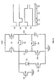
- FIG. 4 shows an embodiment of a bandgap reference circuit having capacitive bias
- FIGS. 5 a through 5 e show different switch states of the circuit of FIG. 4 ;
- FIG. 6 shows exemplary waveforms of the circuit of FIG. 4 ;
- FIG. 7 shows another bandgap reference circuit
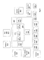
- FIG. 8 shows a computing system
- a solution is to use “capacitive bias” in which first and second charged capacitors behave as the source of potential that drives first and second current densities through a P-N junction.
- the first and second current densities correspond to the pair of current densities whose ratio determines the PTAT voltage.
- the combination of P-N junction and capacitors operate in a region where each of their respective voltage decay behavior varies according to the natural log of time without any substantial dependence on (initial) biasing conditions or parasitics.
- current density ratios can be achieved if one of the capacitors discharges for a small amount of time while the other of the capacitors discharges for a longer amount of time.
- current density ratios of perhaps 4 or 5 orders of magnitude (e.g., 10,000) can be produced which, in turn, corresponds to a significantly larger generated PTAT voltage and a more accurate/stable reference voltage.
- the current densities can be accurately controlled by time, rather than by device sizing.
- FIGS. 1 a and 1 b show a simple capacitor discharge circuit whose behavior corresponds to the capacitive bias principle discussed just above.
- a switch SW is set in a first position that permits a supply voltage VDD to charge a capacitor C.
- the switch is closed in a second position to permit the charged capacitor to discharge into a P-N junction (diode D).
- V D ( t ) ⁇ V T (ln(1 ⁇ (1 ⁇ exp( ⁇ V DD /V T ))(exp( ⁇ I S /( CV T )) t ) Eqn.
- V T is the thermal potential (i.e., kT/q where k is Boltzman's constant, T is the temperature and q is elemental charge)
- V DD is a supply voltage
- I S is the saturation current of the diode
- C is the capacitance of the capacitor
- Eqn. 1 can be approximated as three different equations depending on the value of t. That is, referring to equations 2 a, 2 b and 2 c below, a first equation 2 a approximates Eqn. 1 for small values oft (e.g., less than 50 ns), a second equation 2 b approximates Eqn. 1 for medium values oft (e.g., greater than 50 ns but less than 200 ⁇ s) and a third equation for large values of t (e.g, greater than 200 ⁇ s).
- V D ( t ) ⁇ V T ln((exp( ⁇ V DD /V T )+(( ⁇ I S /( CV T )) t )) Eqn.
- the medium time approximation of Eqn. 2b varies as the natural log of time and does not depend on V DD .
- a bandgap reference voltage circuit can be built that uses the relationship expressed in FIG. 2 b to precisely control the voltage across the PN junction, and, in so doing, precisely control the resulting current density through the PN junction.
- the precise control is effected by precisely controlling the amount of time that the capacitor is allowed to discharge.
- a large dynamic range between the respective current densities that result from their discharge can be realized.
- a large dynamic range between these current densities corresponds to a large current density ratio, which, as described just above, can be used to generate a large PTAT voltage and corresponding accurate/stable output reference voltage.
- FIGS. 2 a through 2 d show the basic principle of operation of a capacitive bias based bandgap reference circuit.
- a first circuit switching state connects a supply voltage V DD to first and second capacitors C 1 , C 2 to charge them approximately to the supply voltage V DD .
- the first phase ends and a second phase begins.
- FIG. 3 shows the behavior of the voltage on both capacitors C 1 and C 2 .
- the voltages of both capacitors C 1 and C 2 charge together in lock stop during the first phase over time T 1 .
- the second phase includes a second switching state in which capacitor C 2 is permitted to discharge through the diode D 1 .
- the amount of time T 2 in which capacitor C 2 is permitted to discharge is tightly controlled and corresponds to a medium amount of time in which the discharge behave is largely defined by Equation 2b above.
- Equation 2b describes decaying voltage behavior that varies as the natural log of the time that the capacitor is permitted to discharge.
- FIG. 3 shows the voltage of capacitor C 2 decaying according to natural log behavior for time T 2 during the second phase.
- the third phase includes a third switching state in which capacitor C 1 is permitted to discharge through the diode D 1 .
- the amount of time T 3 that capacitor C 1 is permitted to discharge is tightly controlled and is within a time period in which the behavior of the discharge is largely described by Eqn. 2b above.
- capacitor C 1 is permitted to discharge for a noticeably longer time period T 3 than capacitor C 2 is permitted to discharge T 2 .
- the voltage of capacitor C 1 decays to a noticeably lower voltage level VD 1 than the level VD 2 that capacitor C 2 decayed to.
- VD 1 , VD 2 corresponds to two significantly different current densities that flow through diode D 1 which, as described at length above, corresponds to a much higher current density ratio than is typical for a bandgap reference voltage circuit.
- current densities having ratios that are on the order of two orders of magnitude (100s), three orders of magnitude (1000s), four orders of magnitude (10000s) or even five orders of magnitude (100000s) are possible.
- the second and third phases and their corresponding controlled capacitor discharge time periods T 2 , T 3 are designed to overlap rather than be disjointed as observed in FIG. 3 (e.g., both phases start at the same time at the end of the first phase with the second phase ending noticeably before the third phase ends).
- V _OUT ( C 2/( C 1+ C 2))( VD 2 ⁇ (( C 1 /C 2) VD 1) Eqn. 3 and where V_OUT further corresponds to the reference voltage generated by the circuit.
- the four phases are continuously repeated to continuously generate the V_OUT reference voltage.
- FIG. 4 shows one embodiment of a circuit that is designed consistently with the principles discussed just above with respect to FIGS. 2 a through 2 d.
- FIGS. 5 a through 5 d show the different switching states of the circuit of FIG. 4 .
- FIG. 6 shows the capacitor voltages.
- transistors P 1 , P 2 and N 1 are on while transistors P 0 , N 2 , N 3 and N 4 are off.
- a direct current path from the supply voltage node to the ground references is established through both capacitors C 1 , C 2 .
- both of the capacitors C 1 , C 2 will be charged approximately to the supply voltage VDD.
- the voltage levels of both capacitors charge together up to the supply voltage within time T 1 .
- the discharge phases of the two capacitors may be overlapped such that they both start discharging at the same time but one of the capacitors stops discharging before the other of the capacitors stops discharging.
- the particular circuit of FIG. 4 conforms to such an approach.
- the second and third phases start at the same time at the end of the first phase.
- the combined second and third phases includes the discharging of the both capacitors C 1 and C 2 into diode D 1 .
- the discharge of capacitor C 2 is effected by turning transistors P 1 and P 2 off, keeping transistors N 3 and N 4 off and turning transistors P 0 and N 2 on.
- the third phase in which capacitor C 1 discharges into diode D 1 , is effected by keeping transistor N 1 on. With this switch state, both capacitors C 1 and C 2 are able to discharge into diode D 1 .
- both of capacitors C 1 and C 2 discharging together, referring to FIG. 6 , note that the voltage of both capacitors fall together according to the logarithmic behavior of Eqn. 2b.
- transistor PO is turned off which prevents any further discharge from capacitor C 2 into diode D 1 .
- C 2 is isolated so that it holds its voltage level VD 2 .
- the third phase continues and capacitor C 1 continues to discharge into diode D 1 . As such, its voltage continues to decay in accordance with Equation 2b.
- a fifth switch state is effected for the fourth phase in which the voltage on capacitor C 1 is subtracted from the voltage on capacitor C 2 to generate an output voltage that corresponds to Eqn. 3 at output node 401 , 501 .
- transistors N 3 and N 4 are turned on and transistor N 1 is turned off. This switching arrangement causes the current path depicted in FIG. 5 e to arise.
- circuits having only one capacitor instead of two capacitors may be implemented.
- the same principle works if a single capacitor is used, where the single capacitor is repeatedly re-charged, then discharged through a diode, and its remaining voltage “transferred” by a suitable charge-transfer mechanism (e.g. a switched-capacitor amplifier] to a summing node/component.
- a suitable charge-transfer mechanism e.g. a switched-capacitor amplifier
- FIG. 5 e shows a parallel combination of +VD 2 and ⁇ VD 1 .
- active circuitry such as a switched-cap amplifier.
- a “charge-transfer” is performed resulting in effective voltage addition (maybe including some scaling and therefore different to Eqn. 3), to reach the same basic function of temperature compensated output voltage
- circuit diagrams discussed above do not depict the circuitry that generates the appropriate signals for switching transistors into an on or off state, it should be understood that such circuits exist and have not been shown purely for illustrative ease.
- FIG. 8 shows a depiction of an exemplary computing system 800 such as a personal computing system (e.g., desktop or laptop) or a mobile or handheld computing system such as a tablet device or smartphone, or, a larger computing system such as a server computing system.
- the computing system may contain a capacitive bias bandgap reference circuit as described above.
- the basic computing system may include a central processing unit 801 (which may include, e.g., a plurality of general purpose processing cores and a main memory controller disposed on an applications processor or multi-core processor), system memory 802 , a display 803 (e.g., touchscreen, flat-panel), a local wired point-to-point link (e.g., USB) interface 804 , various network I/O functions 805 (such as an Ethernet interface and/or cellular modem subsystem), a wireless local area network (e.g., WiFi) interface 806 , a wireless point-to-point link (e.g., Bluetooth) interface 807 and a Global Positioning System interface 808 , various sensors 809 _ 1 through 809 _N (e.g., one or more of a gyroscope, an accelerometer, a magnetometer, a temperature sensor, a pressure sensor, a humidity sensor, etc.), a camera 810 , a battery 811 ,
- the above described capacitive bias bandgap reference circuit may be specifically used, for instance, to generate a reference voltage within a wireless interface circuit such as a cellular/RF interface circuit that is integrated on a system-on-chip having the processing cores and the memory controller.
- An applications processor or multi-core processor 850 may include one or more general purpose processing cores 815 within its CPU 801 , one or more graphical processing units 816 , a memory management function 817 (e.g., a memory controller) and an I/O control function 818 .
- the general purpose processing cores 815 typically execute the operating system and application software of the computing system.
- the graphics processing units 816 typically execute graphics intensive functions to, e.g., generate graphics information that is presented on the display 803 .
- the memory control function 817 interfaces with the system memory 802 .
- the system memory 802 may be a multi-level system memory having, e.g., an emerging three dimensional non-volatile memory technology at at least one of the levels.
- Each of the touchscreen display 803 , the communication interfaces 804 - 807 , the GPS interface 808 , the sensors 809 , the camera 810 , and the speaker/microphone codec 813 , 814 all can be viewed as various forms of I/O (input and/or output) relative to the overall computing system including, where appropriate, an integrated peripheral device as well (e.g., the camera 810 ).
- I/O components may be integrated on the applications processor/multi-core processor 850 or may be located off the die or outside the package of the applications processor/multi-core processor 850 .
- Embodiments of the invention may include various processes as set forth above.
- the processes may be embodied in machine-executable instructions.
- the instructions can be used to cause a general-purpose or special-purpose processor to perform certain processes.
- these processes may be performed by specific hardware components that contain hardwired logic for performing the processes, or by any combination of programmed computer components and custom hardware components.
- Elements of the present invention may also be provided as a machine-readable medium for storing the machine-executable instructions.
- the machine-readable medium may include, but is not limited to, floppy diskettes, optical disks, CD-ROMs, and magneto-optical disks, FLASH memory, ROMs, RAMs, EPROMs, EEPROMs, magnetic or optical cards, propagation media or other type of media/machine-readable medium suitable for storing electronic instructions.
- the present invention may be downloaded as a computer program which may be transferred from a remote computer (e.g., a server) to a requesting computer (e.g., a client) by way of data signals embodied in a carrier wave or other propagation medium via a communication link (e.g., a modem or network connection).
- a remote computer e.g., a server
- a requesting computer e.g., a client
- a communication link e.g., a modem or network connection
Landscapes
- Engineering & Computer Science (AREA)
- Physics & Mathematics (AREA)
- Microelectronics & Electronic Packaging (AREA)
- General Physics & Mathematics (AREA)
- Power Engineering (AREA)
- Nonlinear Science (AREA)
- Electromagnetism (AREA)
- Radar, Positioning & Navigation (AREA)
- Automation & Control Theory (AREA)
- Control Of Electrical Variables (AREA)
- Theoretical Computer Science (AREA)
- General Engineering & Computer Science (AREA)
Abstract
Description
V D(t)=−V T(ln(1−(1−exp(−V DD /V T))(exp(−I S/(CV T))t) Eqn. 1
Where VT is the thermal potential (i.e., kT/q where k is Boltzman's constant, T is the temperature and q is elemental charge), VDD is a supply voltage, IS is the saturation current of the diode, C is the capacitance of the capacitor and t is the time where t=0 when the switch is closed to connect the capacitor C to the diode D.
V D(t)=−V Tln((exp(−V DD /V T)+((−I S/(CV T))t)) Eqn. 2a
V D(t)=−V Tln((I S/(CV T))t)) Eqn. 2b
V D(t)=−V Tln(1−exp(−I S/(CV T))t)) Eqn. 2c
V_OUT=(C2/(C1+C2))(VD2−((C1/C2)VD1) Eqn. 3
and where V_OUT further corresponds to the reference voltage generated by the circuit. Here, the four phases are continuously repeated to continuously generate the V_OUT reference voltage.
Claims (18)
Priority Applications (1)
| Application Number | Priority Date | Filing Date | Title |
|---|---|---|---|
| US15/088,345 US10073483B2 (en) | 2016-04-01 | 2016-04-01 | Bandgap reference circuit with capacitive bias |
Applications Claiming Priority (1)
| Application Number | Priority Date | Filing Date | Title |
|---|---|---|---|
| US15/088,345 US10073483B2 (en) | 2016-04-01 | 2016-04-01 | Bandgap reference circuit with capacitive bias |
Publications (2)
| Publication Number | Publication Date |
|---|---|
| US20170285680A1 US20170285680A1 (en) | 2017-10-05 |
| US10073483B2 true US10073483B2 (en) | 2018-09-11 |
Family
ID=59960917
Family Applications (1)
| Application Number | Title | Priority Date | Filing Date |
|---|---|---|---|
| US15/088,345 Active US10073483B2 (en) | 2016-04-01 | 2016-04-01 | Bandgap reference circuit with capacitive bias |
Country Status (1)
| Country | Link |
|---|---|
| US (1) | US10073483B2 (en) |
Families Citing this family (2)
| Publication number | Priority date | Publication date | Assignee | Title |
|---|---|---|---|---|
| US11015985B2 (en) | 2018-03-30 | 2021-05-25 | Intel IP Corporation | Time-controlled switch capacitor based temperature sensor |
| US11493968B2 (en) * | 2019-08-09 | 2022-11-08 | Intel Corporation | Reverse bandgap reference circuit with bulk diode, and switch capacitor temperature sensor with duty-cycle output |
Citations (10)
| Publication number | Priority date | Publication date | Assignee | Title |
|---|---|---|---|---|
| US20070096702A1 (en) * | 2005-10-27 | 2007-05-03 | Rasmus Todd M | Regulator with load tracking bias |
| US20120169413A1 (en) * | 2010-12-30 | 2012-07-05 | Stmicroelectronics Inc. | Bandgap voltage reference circuit, system, and method for reduced output curvature |
| US20130228773A1 (en) * | 2012-03-02 | 2013-09-05 | Semiconductor Energy Laboratory Co., Ltd. | Memory device and semiconductor device including the same |
| US20140139246A1 (en) * | 2012-11-19 | 2014-05-22 | Taiwan Semiconductor Manufacturing Company, Ltd. | Wafer Temperature Sensing Methods and Related Semiconductor Wafer |
| US8816756B1 (en) | 2013-03-13 | 2014-08-26 | Intel Mobile Communications GmbH | Bandgap reference circuit |
| US9013231B1 (en) * | 2013-12-06 | 2015-04-21 | Atmel Corporation | Voltage reference with low sensitivity to package shift |
| US9122290B2 (en) | 2013-03-15 | 2015-09-01 | Intel Deutschland Gmbh | Bandgap reference circuit |
| US20150310932A1 (en) * | 2014-04-29 | 2015-10-29 | Chris P. Nappi | Semiconductor device having a test controller and method of operation |
| US20150365112A1 (en) * | 2014-06-16 | 2015-12-17 | Skyworks Solutions, Inc. | Band-gap reference circuit for biasing an rf device |
| US9240775B2 (en) | 2013-03-12 | 2016-01-19 | Intel Deutschland Gmbh | Circuit arrangements |
-
2016
- 2016-04-01 US US15/088,345 patent/US10073483B2/en active Active
Patent Citations (10)
| Publication number | Priority date | Publication date | Assignee | Title |
|---|---|---|---|---|
| US20070096702A1 (en) * | 2005-10-27 | 2007-05-03 | Rasmus Todd M | Regulator with load tracking bias |
| US20120169413A1 (en) * | 2010-12-30 | 2012-07-05 | Stmicroelectronics Inc. | Bandgap voltage reference circuit, system, and method for reduced output curvature |
| US20130228773A1 (en) * | 2012-03-02 | 2013-09-05 | Semiconductor Energy Laboratory Co., Ltd. | Memory device and semiconductor device including the same |
| US20140139246A1 (en) * | 2012-11-19 | 2014-05-22 | Taiwan Semiconductor Manufacturing Company, Ltd. | Wafer Temperature Sensing Methods and Related Semiconductor Wafer |
| US9240775B2 (en) | 2013-03-12 | 2016-01-19 | Intel Deutschland Gmbh | Circuit arrangements |
| US8816756B1 (en) | 2013-03-13 | 2014-08-26 | Intel Mobile Communications GmbH | Bandgap reference circuit |
| US9122290B2 (en) | 2013-03-15 | 2015-09-01 | Intel Deutschland Gmbh | Bandgap reference circuit |
| US9013231B1 (en) * | 2013-12-06 | 2015-04-21 | Atmel Corporation | Voltage reference with low sensitivity to package shift |
| US20150310932A1 (en) * | 2014-04-29 | 2015-10-29 | Chris P. Nappi | Semiconductor device having a test controller and method of operation |
| US20150365112A1 (en) * | 2014-06-16 | 2015-12-17 | Skyworks Solutions, Inc. | Band-gap reference circuit for biasing an rf device |
Non-Patent Citations (2)
| Title |
|---|
| Hellen, E., "Verifying the Diode-Capacitor Circuit Voltage Decay", American Journal of Physics, vol. 71, No. 8, Aug. 2003, pp. 797-800. |
| Prior Art CMOS Bandgap Voltage Reference, Mar. 1, 2016. |
Also Published As
| Publication number | Publication date |
|---|---|
| US20170285680A1 (en) | 2017-10-05 |
Similar Documents
| Publication | Publication Date | Title |
|---|---|---|
| US9235229B2 (en) | Low power fast settling voltage reference circuit | |
| US9557226B2 (en) | Current-mode digital temperature sensor apparatus | |
| US9606563B2 (en) | Bandgap reference voltage failure detection | |
| US20150168969A1 (en) | Accurate power-on detector | |
| US9939832B2 (en) | Voltage regulator and integrated circuit including the same | |
| CN112835409B (en) | Bandgap reference voltage generation circuit | |
| TWI443672B (en) | Adjusting the charge pump regulator and its memory circuit | |
| US10788376B2 (en) | Apparatus for sensing temperature in electronic circuitry and associated methods | |
| US20160191041A1 (en) | Circuit and Method for Power-On Reset of an Integrated Circuit | |
| US9665116B1 (en) | Low voltage current mode bandgap circuit and method | |
| US11493968B2 (en) | Reverse bandgap reference circuit with bulk diode, and switch capacitor temperature sensor with duty-cycle output | |
| US10296025B2 (en) | Apparatus for electric current measurement or calibration and associated methods | |
| WO2015047303A1 (en) | Digital switch-capacitor based bandgap reference and thermal sensor | |
| US10921377B2 (en) | Fuel gauge system for measuring the amount of current in battery and portable electronic device including the same | |
| US9690578B2 (en) | High dose radiation detector | |
| US10359799B2 (en) | Bandgap reference voltage generation circuit and bandgap reference voltage generation system | |
| US11015985B2 (en) | Time-controlled switch capacitor based temperature sensor | |
| US20170285680A1 (en) | Bandgap reference circuit with capacitive bias | |
| KR102048214B1 (en) | Ambient light sensor and electronic system having the same | |
| Hasler | Energy-efficient programable analog computing: Analog computing in a standard cmos process | |
| WO2019028595A1 (en) | Oscillator, integrated circuit, timing chip, and electronic device | |
| US9257194B1 (en) | Drain regulator for NOR flash memory | |
| CN108205349A (en) | A kind of band-gap reference circuit | |
| US20170269626A1 (en) | Reference voltage generator and voltage generating system having the same | |
| US8120971B2 (en) | Internal source voltage generating circuit of semiconductor memory device |
Legal Events
| Date | Code | Title | Description |
|---|---|---|---|
| AS | Assignment |
Owner name: INTEL CORPORATION, CALIFORNIA Free format text: ASSIGNMENT OF ASSIGNORS INTEREST;ASSIGNOR:EBERLEIN, MATTHIAS;REEL/FRAME:038645/0436 Effective date: 20160421 |
|
| STCF | Information on status: patent grant |
Free format text: PATENTED CASE |
|
| MAFP | Maintenance fee payment |
Free format text: PAYMENT OF MAINTENANCE FEE, 4TH YEAR, LARGE ENTITY (ORIGINAL EVENT CODE: M1551); ENTITY STATUS OF PATENT OWNER: LARGE ENTITY Year of fee payment: 4 |
|
| FEPP | Fee payment procedure |
Free format text: MAINTENANCE FEE REMINDER MAILED (ORIGINAL EVENT CODE: REM.); ENTITY STATUS OF PATENT OWNER: LARGE ENTITY |