US10073200B2 - Nano-gap grating devices with enhanced optical properties and methods of fabrication - Google Patents
Nano-gap grating devices with enhanced optical properties and methods of fabrication Download PDFInfo
- Publication number
- US10073200B2 US10073200B2 US14/081,353 US201314081353A US10073200B2 US 10073200 B2 US10073200 B2 US 10073200B2 US 201314081353 A US201314081353 A US 201314081353A US 10073200 B2 US10073200 B2 US 10073200B2
- Authority
- US
- United States
- Prior art keywords
- functional layer
- grating structure
- grating
- ink
- nanogap
- Prior art date
- Legal status (The legal status is an assumption and is not a legal conclusion. Google has not performed a legal analysis and makes no representation as to the accuracy of the status listed.)
- Active, expires
Links
- 239000000758 substrate Substances 0.000 claims abstract description 51
- 239000002346 layers by function Substances 0.000 claims description 77
- 239000010410 layer Substances 0.000 claims description 72
- 229910052751 metal Inorganic materials 0.000 claims description 46
- 239000002184 metal Substances 0.000 claims description 46
- 230000008021 deposition Effects 0.000 claims description 12
- 239000011521 glass Substances 0.000 claims description 10
- 229910001092 metal group alloy Inorganic materials 0.000 claims 2
- 239000000463 material Substances 0.000 abstract description 39
- 238000000034 method Methods 0.000 abstract description 21
- 229920006254 polymer film Polymers 0.000 abstract description 10
- 230000000737 periodic effect Effects 0.000 abstract description 7
- 229920002457 flexible plastic Polymers 0.000 abstract description 4
- 230000003287 optical effect Effects 0.000 description 36
- 238000000151 deposition Methods 0.000 description 9
- 230000005672 electromagnetic field Effects 0.000 description 8
- BQCADISMDOOEFD-UHFFFAOYSA-N Silver Chemical group [Ag] BQCADISMDOOEFD-UHFFFAOYSA-N 0.000 description 7
- 229920003023 plastic Polymers 0.000 description 7
- 239000004033 plastic Substances 0.000 description 7
- 229920003217 poly(methylsilsesquioxane) Polymers 0.000 description 7
- 229910052709 silver Inorganic materials 0.000 description 7
- 239000004332 silver Substances 0.000 description 7
- 239000002904 solvent Substances 0.000 description 6
- 238000004519 manufacturing process Methods 0.000 description 5
- 150000002739 metals Chemical class 0.000 description 5
- XUIMIQQOPSSXEZ-UHFFFAOYSA-N Silicon Chemical compound [Si] XUIMIQQOPSSXEZ-UHFFFAOYSA-N 0.000 description 4
- 238000001506 fluorescence spectroscopy Methods 0.000 description 4
- 238000003384 imaging method Methods 0.000 description 4
- 239000010703 silicon Substances 0.000 description 4
- 229910052710 silicon Inorganic materials 0.000 description 4
- GWEVSGVZZGPLCZ-UHFFFAOYSA-N Titan oxide Chemical compound O=[Ti]=O GWEVSGVZZGPLCZ-UHFFFAOYSA-N 0.000 description 3
- 239000003989 dielectric material Substances 0.000 description 3
- 238000005516 engineering process Methods 0.000 description 3
- 239000002861 polymer material Substances 0.000 description 3
- 239000007787 solid Substances 0.000 description 3
- LFQSCWFLJHTTHZ-UHFFFAOYSA-N Ethanol Chemical compound CCO LFQSCWFLJHTTHZ-UHFFFAOYSA-N 0.000 description 2
- GRYLNZFGIOXLOG-UHFFFAOYSA-N Nitric acid Chemical compound O[N+]([O-])=O GRYLNZFGIOXLOG-UHFFFAOYSA-N 0.000 description 2
- VYPSYNLAJGMNEJ-UHFFFAOYSA-N Silicium dioxide Chemical compound O=[Si]=O VYPSYNLAJGMNEJ-UHFFFAOYSA-N 0.000 description 2
- RTAQQCXQSZGOHL-UHFFFAOYSA-N Titanium Chemical compound [Ti] RTAQQCXQSZGOHL-UHFFFAOYSA-N 0.000 description 2
- 238000005452 bending Methods 0.000 description 2
- 230000008901 benefit Effects 0.000 description 2
- 238000000701 chemical imaging Methods 0.000 description 2
- 238000005520 cutting process Methods 0.000 description 2
- 238000001514 detection method Methods 0.000 description 2
- 238000010586 diagram Methods 0.000 description 2
- 239000004205 dimethyl polysiloxane Substances 0.000 description 2
- 239000012634 fragment Substances 0.000 description 2
- 239000007788 liquid Substances 0.000 description 2
- 229910017604 nitric acid Inorganic materials 0.000 description 2
- 229920000435 poly(dimethylsiloxane) Polymers 0.000 description 2
- 229920000642 polymer Polymers 0.000 description 2
- 238000004528 spin coating Methods 0.000 description 2
- 239000000126 substance Substances 0.000 description 2
- 229910052719 titanium Inorganic materials 0.000 description 2
- 239000010936 titanium Substances 0.000 description 2
- OGIDPMRJRNCKJF-UHFFFAOYSA-N titanium oxide Inorganic materials [Ti]=O OGIDPMRJRNCKJF-UHFFFAOYSA-N 0.000 description 2
- VYZAMTAEIAYCRO-UHFFFAOYSA-N Chromium Chemical compound [Cr] VYZAMTAEIAYCRO-UHFFFAOYSA-N 0.000 description 1
- 229910045601 alloy Inorganic materials 0.000 description 1
- 239000000956 alloy Substances 0.000 description 1
- 239000003124 biologic agent Substances 0.000 description 1
- 230000015572 biosynthetic process Effects 0.000 description 1
- 239000013043 chemical agent Substances 0.000 description 1
- 229910052804 chromium Inorganic materials 0.000 description 1
- 239000011651 chromium Substances 0.000 description 1
- 239000011248 coating agent Substances 0.000 description 1
- 238000000576 coating method Methods 0.000 description 1
- 238000013500 data storage Methods 0.000 description 1
- 230000001066 destructive effect Effects 0.000 description 1
- 230000000694 effects Effects 0.000 description 1
- 238000000609 electron-beam lithography Methods 0.000 description 1
- 230000002708 enhancing effect Effects 0.000 description 1
- 238000005530 etching Methods 0.000 description 1
- 238000000799 fluorescence microscopy Methods 0.000 description 1
- PCHJSUWPFVWCPO-UHFFFAOYSA-N gold Chemical compound [Au] PCHJSUWPFVWCPO-UHFFFAOYSA-N 0.000 description 1
- 229910052737 gold Inorganic materials 0.000 description 1
- 239000010931 gold Substances 0.000 description 1
- 238000000227 grinding Methods 0.000 description 1
- 230000003760 hair shine Effects 0.000 description 1
- 239000013056 hazardous product Substances 0.000 description 1
- 239000011810 insulating material Substances 0.000 description 1
- 230000010354 integration Effects 0.000 description 1
- 238000003754 machining Methods 0.000 description 1
- 238000005272 metallurgy Methods 0.000 description 1
- 238000012634 optical imaging Methods 0.000 description 1
- 238000000059 patterning Methods 0.000 description 1
- 239000004038 photonic crystal Substances 0.000 description 1
- 238000001020 plasma etching Methods 0.000 description 1
- 239000004417 polycarbonate Substances 0.000 description 1
- 229920000515 polycarbonate Polymers 0.000 description 1
- -1 polydimethylsiloxane Polymers 0.000 description 1
- 235000012239 silicon dioxide Nutrition 0.000 description 1
- 239000000377 silicon dioxide Substances 0.000 description 1
- 238000003980 solgel method Methods 0.000 description 1
- 238000004611 spectroscopical analysis Methods 0.000 description 1
- 238000006467 substitution reaction Methods 0.000 description 1
- 238000004416 surface enhanced Raman spectroscopy Methods 0.000 description 1
Images


Classifications
-
- G—PHYSICS
- G02—OPTICS
- G02B—OPTICAL ELEMENTS, SYSTEMS OR APPARATUS
- G02B5/00—Optical elements other than lenses
- G02B5/18—Diffraction gratings
- G02B5/1842—Gratings for image generation
-
- G—PHYSICS
- G02—OPTICS
- G02B—OPTICAL ELEMENTS, SYSTEMS OR APPARATUS
- G02B5/00—Optical elements other than lenses
- G02B5/18—Diffraction gratings
-
- G—PHYSICS
- G02—OPTICS
- G02B—OPTICAL ELEMENTS, SYSTEMS OR APPARATUS
- G02B5/00—Optical elements other than lenses
- G02B5/18—Diffraction gratings
- G02B5/1814—Diffraction gratings structurally combined with one or more further optical elements, e.g. lenses, mirrors, prisms or other diffraction gratings
-
- G—PHYSICS
- G02—OPTICS
- G02B—OPTICAL ELEMENTS, SYSTEMS OR APPARATUS
- G02B5/00—Optical elements other than lenses
- G02B5/18—Diffraction gratings
- G02B5/1847—Manufacturing methods
- G02B5/1852—Manufacturing methods using mechanical means, e.g. ruling with diamond tool, moulding
-
- G—PHYSICS
- G02—OPTICS
- G02B—OPTICAL ELEMENTS, SYSTEMS OR APPARATUS
- G02B5/00—Optical elements other than lenses
- G02B5/18—Diffraction gratings
- G02B5/1861—Reflection gratings characterised by their structure, e.g. step profile, contours of substrate or grooves, pitch variations, materials
Definitions
- Embodiments of the invention relate to structures for improving optical imaging and methods of their fabrication.
- Microscopic imaging is utilized for studying small objects in fields such as medical development, biological research, cancer research, metallurgy, and others. Imaging of microscopic objects often encounters the diffraction limit when trying to image increasingly small objects. Fluorescence spectroscopy can be utilized in ultrasensitive chemical and biological threat sensors. But fluorescence spectroscopy suffers from low image contrast and a limit on the detection capabilities. Uniform, periodic grating structures have been developed to offer improvement in microscopic imaging and fluorescence spectroscopy. However, the improvements may be limited and the production of the grating structures may require the usage of costly fabrication equipment and complex manufacturing techniques, leading to a high cost of the grating structures.
- Embodiments of the invention solve the above-mentioned problems and provide a distinct advance in the art of microscopic imaging and fluorescence spectroscopy. More particularly, embodiments of the invention provide grating structures with enhanced optical properties and methods of their fabrication.
- a first embodiment of the invention provides a grating structure comprising a substrate, a base layer, and a first functional layer.
- the base layer is positioned on the substrate and includes a first surface with a plurality of grating elements positioned adjacent one another and an opposing second surface in contact with a surface of the substrate.
- the grating elements include a longitudinal peak and a longitudinal valley.
- the functional layer is positioned on the second surface of the base layer and provides electromagnetic field enhancement in the vicinity of the grating structure.
- a second embodiment of the invention provides a method of producing a grating structure.
- the method comprises the steps of forming a stamp from flexible plastic material, the stamp including a negative of a periodic grating pattern on a first surface; forming an ink by applying a polymer film to the stamp, the ink including a first surface and an opposing second surface, wherein the first surface of the ink contacts the first surface of the stamp such that the ink retains a positive of the periodic grating pattern; placing the ink and the stamp on a substrate such that the second surface of the ink contacts an upper surface of the substrate; and removing the stamp from the ink by applying a tensional force to one edge of the stamp.
- a third embodiment of the invention provides a method of producing a.
- the method comprises the steps of forming a stamp by applying a flexible plastic material to a mold which includes a periodic grating pattern, wherein the stamp retains a negative of the grating pattern on a first surface; forming an ink by applying a polymer film to the stamp, the ink including a first surface and an opposing second surface, wherein the first surface of the ink contacts the first surface of the stamp such that the ink retains a positive of the periodic grating pattern; placing the ink and the stamp on a substrate such that the second surface of the ink contacts an upper surface of the substrate; removing the stamp from the ink by applying a tensional force to one edge of the stamp; and applying a functional layer to the first surface of the ink.
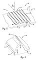
- FIG. 1 is a perspective view of a grating structure including a first functional layer, a base layer, and a substrate, constructed in accordance with various embodiments of the invention
- FIG. 5 is a perspective view of the grating structure with the first functional layer being deposited normal to the plane of the grating structure and a second functional layer being deposited at an angle away from normal to the plane of the grating structure;
- FIG. 6 is an enlarged view of a portion of the grating structure of FIG. 5 ;
- FIG. 7 is a flow diagram of at least a portion of the steps of a method of producing a grating structure
- FIG. 8 is a perspective view of a mold created from a modified optical disc
- FIG. 9 is a perspective view of the mold coated with a plastic material to form a stamp
- FIG. 10 is a sectional view of the mold and the stamp from FIG. 9 cut along the line 10 - 10 ;
- FIG. 11 is a perspective view of the mold and the stamp with a portion of the stamp removed to create a small stamp
- FIG. 12 is a perspective view of the stamp placed on a temporary substrate
- FIG. 13 is a perspective view of the stamp on the temporary substrate coated with a polymer film to create an ink
- FIG. 14 is a sectional view of the stamp and the ink from FIG. 13 cut along the line 14 - 14 ;
- FIG. 15 is a perspective view of the stamp and the ink placed on a permanent substrate
- FIG. 16 is a sectional view of the stamp and the ink from FIG. 15 cut along the line 16 - 16 ;
- FIG. 17 is a perspective view of the stamp and the ink on the permanent substrate depicting the stamp being removed from the ink;
- FIG. 18 is a flow diagram of at least a portion of the steps of a method of producing a mold that includes a grating structure
- FIG. 19 is a sectional view of a first type of optical disc with a metal layer and a transparent side in which the metal layer is closer to the transparent side;
- FIG. 20 is a sectional view of the first type of optical disc in which the metal layer and the transparent side have been removed;
- FIG. 21 is a sectional view of a second type of optical disc with a metal layer, a transparent side, and a label side in which the metal layer is not closer to the transparent side;
- FIG. 22 is a sectional view of the second type of optical disc in which the metal layer and the label side have been removed.
- references to “one embodiment”, “an embodiment”, or “embodiments” mean that the feature or features being referred to are included in at least one embodiment of the technology.
- references to “one embodiment”, “an embodiment”, or “embodiments” in this description do not necessarily refer to the same embodiment and are also not mutually exclusive unless so stated and/or except as will be readily apparent to those skilled in the art from the description.
- a feature, structure, act, etc. described in one embodiment may also be included in other embodiments, but is not necessarily included.
- the technology can include a variety of combinations and/or integrations of the embodiments described herein.
- a grating structure 10 with nanogap features, constructed in accordance with various embodiments of the invention, is shown in FIGS. 1, 3, and 4 and may broadly comprise a substrate 12 and an array 14 of grating elements 16 .
- Various embodiments of the invention can provide optical wave guiding and imaging beyond the diffraction limit.
- the invention may be utilized in a sensing or imaging system which may improve the detection limits of harmful biological and chemical agents in food down to pico or femtomolar concentration levels.
- the invention may be used in anti-terrorism to detect any trace quantities of bio or chemically hazardous material.
- Embodiments of the invention may also be utilized in studying single molecule fluorescence phenomena in real time, enhancing surface-enhanced Raman spectroscopy (SERS), and the like.
- SERS surface-enhanced Raman spectroscopy
- the substrate 12 generally provides a structural base or foundational support for the grating elements 16 and may be formed from silicon, glass, or combinations thereof.
- the substrate 12 may include an upper surface 18 that receives the grating elements 16 .
- the upper surface 18 may be planar and smooth so as to easily bond with the grating elements 16 .
- the array 14 is arranged on the substrate 12 so that the grating elements 16 are parallel and positioned abutting one another.
- Each grating element 16 is generally elongated, relatively narrow, and is formed with a longitudinal peak 20 positioned next to a longitudinal valley 22 .
- the longitudinal axis of the grating elements 16 may be straight, while in other embodiments, the longitudinal axis may be curved.
- the peak 20 may have a constant and continuous height along the length of the grating element 16 , while in other embodiments, the peak 20 may have a variable height along the length of the grating element 16 .
- An exemplary grating element 16 may have a cross-sectional profile that is a roughly half sine wave with the peak 20 having a generally rounded shape and the valley 22 being generally flat.
- An exemplary grating element 16 may have a width or pitch of approximately 400 nanometers (nm). The width of each grating element 16 may vary depending on the application for which the grating structure 10 is used.
- An exemplary peak 20 may have a height relative to the valley 22 of approximately 60 nm.
- the grating element 16 may have a cross-sectional profile that is a roughly sine wave shape, a roughly triangle wave shape, a roughly square wave shape, a roughly sawtooth shape, variations thereof, or combinations thereof.
- Each grating element 16 may include a base layer 24 and a first functional layer 26 .
- the base layer 24 as seen without the first functional layer 26 in FIG. 2 , may be positioned on the substrate 12 and may include a lower surface 28 which contacts and adheres to the upper surface 18 of the substrate 12 .
- the base layer 24 may be formed from a polymer material or a polymer film such as polymethylsilsesquioxane (PMSSQ) and may have the same cross-sectional profile as the grating element 16 including the peak 20 and the valley 22 .
- the base layer 24 may also be considered an ink.
- the base layer 24 may further include a plurality of nanogaps 30 , best seen in FIG. 2 , wherein each nanogap 30 is an elongated, generally narrow gap or opening in the material of the base layer 24 .
- Exemplary nanogaps 30 may have a width ranging from approximately 20 nm to approximately 30 nm, while the length of the nanogaps 30 may vary more greatly.
- the nanogaps 30 may be randomly oriented and randomly distributed primarily in proximity to the edges of the array 14 .
- the nanogaps 30 may be more uniformly distributed across the array 14 .
- the nanogaps 30 may generally be oriented or aligned with one another. In still other embodiments, there may be a combination of randomly oriented and distributed nanogaps 30 and more uniformly oriented and distributed nanogaps 30 .
- the first functional layer 26 generally provides electromagnetic field enhancement in the vicinity of the grating structure 10 .
- the first functional layer 26 may be applied or formed such that it does not fill in or completely cover the nanogaps 30 of the base layer 24 .
- the first functional layer 26 may include either a plasmonic component or a photonic component.
- the first functional layer 26 primarily includes one or more layers of metal.
- An optional lower metal layer may provide improved adhesion between the base layer 24 and an upper layer of metal.
- An exemplary lower metal layer may include a thin layer of titanium, approximately 2 nm thick.
- a main upper layer of metal may provide plasmonic functionality.
- An exemplary metal for the upper metal layer is silver, approximately 100 nm thick, deposited on the first lower layer of metal.
- Silver is often utilized as the plasmonic material because it may allow or promote fluorescence in various applications of the grating structure 10 to a greater extent than other metals.
- silver may have a lower energy loss than other metals.
- Other metals can be used for either the first lower adhesion layer or the second, upper metal layer including silver, titanium, gold, chromium, alloys, or combinations thereof.
- the plasmonic first functional layer 26 may further include a thin layer of dielectric or insulating material, such as silicon dioxide, rhodamine-doped PMSSQ, or similar materials positioned on the metal.
- the layer of dielectric may have a thickness ranging from approximately 10 nm to approximately 30 nm.
- the first functional layer 26 primarily includes one or more layers of dielectrics.
- An exemplary photonic first functional layer may include titanium oxide (TiO 2 ), with a thickness ranging from approximately 100 nm to approximately 200 nm, deposited on the base layer 24 .
- TiO 2 titanium oxide
- the thickness of the base layer 24 may be varied as well to provide different performance characteristics.
- the first functional layer 26 may further include nanogaps 32 as well, seen in FIGS. 3 and 4 , depending on the angle of deposition of the plasmonic or photonic material onto the base layer 24 . If the plasmonic or photonic material of the first functional layer 26 is deposited onto the base layer 24 at an angle that is roughly normal to the plane of the substrate 12 and the base layer 24 , as shown in FIG. 1 , then no nanogaps 32 in the first functional layer 26 are formed. If the plasmonic or photonic material is deposited at an angle, such as ⁇ shown in FIG. 3 , away from the normal, then nanogaps 32 may be formed in parallel with the grating elements 16 .
- the deposition angle may range from approximately zero degrees to approximately 85 degrees from planar normal, with a range from approximately 65 degrees to approximately 80 degrees providing optimal results.
- the plasmonic or photonic material is also deposited in a direction that is transverse to the longitudinal axis of the grating elements 16 .
- each grating element 16 may include three regions, as seen in FIGS. 3 and 4 , instead of just the two discussed above.
- the regions may include the nanogap 32 , a tip 34 , and a plateau 36 .
- the tip 34 may include a plurality of nanospurs 58 .
- the nanogap 32 may present a low point for the grating element 16
- the tip 34 may present a high point, with an angled, generally smooth surface therebetween.
- the plateau 36 may have a rounded shape that falls from the tip of one grating element 16 to the nanogap 32 of the adjacent grating element 16 .
- the nanogap 32 has a width ranging from approximately 10 nm to approximately 30 nm
- the tip 34 has a width ranging from approximately 10 nm to approximately 30 nm
- the plateau 36 has a width of approximately 90 nm.
- the nanospurs 58 may include or may form a plurality of peaks abutting one another along the length of the tip 34 , as shown in FIGS. 3-6 .
- Each nanospur 58 may have a shape of roughly a triangle, roughly a sawtooth, roughly a half sine wave, variations thereof, or combinations thereof. At the edges of each nanospur 58 , or where the nanospurs 58 join with one another, there may be a sharp point.
- the nanogap 32 and the tip 34 may behave like electromagnetic field concentrators, wherein the nanogap 32 acts as a lightning rod and the tip 34 acts as a nano antenna.
- the plateau 36 experiences interference from the two distinct electromagnetic fields resulting in either constructive or destructive interference.
- the large electromagnetic fields produced in the nanogap 30 , the tip 34 , and the plateau 36 are a result of the localized electromagnetic field enhancement.
- the grating structure 10 is utilized in fluorescence imaging, either the lightning rod, the nano antenna, or the constructive interference effect may cause any fluorophore placed in the right region to fluoresce with a several fold higher intensity in comparison to the other regions.
- the nanospurs 58 positioned along the tips 34 may enhance or amplify the electromagnetic field to create regions along the grating structure 10 with an increased electromagnetic field known as hotspots.
- the grating structure 10 may further include a second functional layer 60 , as seen in FIGS. 5 and 6 , positioned on the upper surface of the first functional layer 26 .
- the first functional layer 26 is a photonic material functional layer 26 wherein the photonic material is a dielectric such as titanium oxide.
- the first functional layer 26 is deposited at angle of approximately zero degrees from planar normal, so that the first functional layer 26 may have a shape as seen in FIG. 1 .
- the second functional layer 60 typically includes plasmonic material such as silver that is deposited at an angle ranging from greater than zero degrees to approximately 85 degrees from planar normal.
- both the first functional layer 26 and the second functional layer 60 may include plasmonic materials.
- FIG. 7 At least a portion of the steps of a method 100 , in accordance with various aspects of the invention, for producing a grating structure 10 is shown in FIG. 7 .
- the steps of the method 100 may be performed in the order as shown in FIG. 7 , or they may be performed in a different order. Furthermore, some steps may be performed concurrently as opposed to sequentially. In addition, some steps may not be performed.
- a stamp 38 is formed by applying a flexible plastic material to a mold 40 , shown in FIG. 8 , which includes a grating pattern 42 such that the plastic material receives and retains a negative of the grating pattern 42 .
- the plastic material may include any flexible, somewhat resilient polymer that can adapt to the shape of a mold and retain that shape.
- An exemplary plastic material is polydimethylsiloxane (PDMS).
- the mold 40 may be any solid object that includes the grating pattern 42 on one of its surfaces and may be constructed from materials such as metals, glass, silicon, or the like.
- the mold 40 may be produced by an exemplary process described below or by forming the grating pattern 42 in the mold 40 material using patterning and etching, e-beam lithography, reactive ion etching, machining, or the like.
- An exemplary mold 40 is an optical disc, such as a compact disc (CD), a digital video disc (DVD), a high definition DVD (HD-DVD), a Blu-rayTM disc, etc., which includes an internal data layer defined by a grating pattern, the same as or similar to the grating pattern 42 , with a portion of the disc removed to expose the data layer and the grating pattern, as seen in FIG. 8 .
- an optical disc such as a compact disc (CD), a digital video disc (DVD), a high definition DVD (HD-DVD), a Blu-rayTM disc, etc.
- the grating pattern 42 may be similar to the array 14 , discussed above, wherein the grating pattern 42 includes a plurality of grating elements 16 with the characteristics mentioned above.
- the grating elements 16 of an exemplary grating pattern 42 may include a longitudinal peak 20 positioned next to a longitudinal valley 22 that in combination have a cross-sectional width of approximately 400 nm.
- the plastic material that forms the stamp 38 may initially be in a liquid form and may be applied to the surface of the mold 40 that includes the grating pattern 42 by spin coating the plastic material onto the mold 40 in a known fashion, the result of which is shown in FIGS. 9 and 10 .
- the plastic material may cure on the mold 40 until it hardens and is solid to the touch—thereby forming the stamp 38 .
- the stamp 38 is removed from the mold 40 and is placed on a temporary substrate 44 .
- the temporary substrate 44 is generally a rigid body with at least one surface that is flat and smooth.
- An exemplary temporary substrate 44 is a glass slide, a silicon wafer, or the like.
- the stamp 38 may include a first surface 46 which includes the negative of the grating pattern 42 and an opposing second surface 48 which is generally flat and smooth.
- the stamp 38 is placed on the temporary substrate 44 such that the second surface 48 contacts the temporary substrate 44 and the first surface 46 is exposed and accessible, as seen in FIG. 12 .
- an ink 50 is formed by applying a polymer film to the stamp 38 to receive and retain a positive of the grating pattern 42 .
- the polymer film may include any flexible, somewhat resilient polymer that can adapt to the shape of a mold and retain that shape.
- An exemplary polymer film is polymethylsilsesquioxane (PMSSQ).
- the PMSSQ may be mixed with ethanol.
- the polymer film that forms the ink 50 may initially be in a liquid form and may be applied to the stamp 38 by spin coating onto the exposed first surface 46 , the result of which is shown in FIGS. 13 and 14 .
- the polymer film may cure on the stamp 38 until it hardens and is solid to the touch—thereby forming the ink 50 .
- the ink 50 may include a first surface 52 and an opposing second surface 54 , as best seen in FIG. 14 .
- the first surface 52 includes the positive of the grating pattern 42 and is in contact with the first surface 46 of the stamp 38 .
- the second surface 54 is generally flat and smooth.
- nanogaps 30 are created in the ink 50 , similar to those of the base layer 24 seen in FIG. 2 .
- the nanogaps 30 may include tears, openings, or gaps in the polymer material of the ink 50 .
- Exemplary nanogaps 30 may have a width ranging from approximately 20 nm to approximately 30 nm, while the length of the nanogaps 30 may vary more greatly.
- the nanogaps 30 may be formed by applying a tensional force to opposing ends of the stamp 38 and the ink 50 while they are in contact with one another.
- the nanogaps 30 may also be formed by poking holes in the combination of the stamp 38 and the ink 50 , by bending the combination of the stamp 38 and the ink 50 , or by reverse bending the combination of the stamp 38 and the ink 50 .
- This step may be optional, it may be performed after the stamp 38 and ink 50 are removed from the temporary substrate 44 , or it may be performed during or after step 105 .
- the stamp 38 and the ink 50 are removed from the temporary substrate 44 and placed on a permanent substrate 56 , as shown in FIGS. 15 and 16 .
- the permanent substrate 56 may be similar to the temporary substrate 44 .
- An exemplary permanent substrate 56 is a glass slide, a silicon wafer, or the like.
- the stamp 38 and ink 50 may be removed from the temporary substrate 44 as a unit while still contacting one another. They may be removed manually by a technician or by an automated machine.
- the stamp 38 and ink 50 may be placed on the permanent substrate 56 with the second surface of the ink 50 contacting a surface of the permanent substrate 56 and the second surface of the stamp 38 facing away from the permanent substrate 56 . The placement may be performed manually or by automated machine. After the placement of the stamp 38 and ink 50 , a period of time may elapse to allow the ink 50 to seal with the permanent substrate 56 .
- the stamp 38 is removed from the ink 50 .
- the stamp 38 may be peeled from the ink 50 by manually lifting one corner or edge of the stamp 38 , as seen in FIG. 17 , with a pair of tweezers.
- the stamp 38 may be removed from the ink 50 by an automated machine. The process of removing the stamp 38 from the ink 50 may create nanogaps 30 in the stamp 38 which are transferred to the ink 50 .
- the ink 50 may a plurality of nanogaps 30 that are randomly oriented and generally positioned in proximity to the perimeter of the ink 50 .
- the first surface 52 of the ink 50 is exposed such that the positive of the grating pattern 42 is facing upwards.
- the ink 50 on the permanent substrate 56 generally forms the base layer 24 on the substrate 12 of the grating structure 10 .
- a first functional layer 26 is applied to the ink 50 .
- the first functional layer 26 is applied to the first surface 52 on top of the grating pattern 42 .
- the first functional layer 26 may include plasmonic material, such as metals, or photonic material, such as dielectrics, as discussed above.
- the first functional layer 26 may be applied to the ink 50 using known deposition techniques.
- the first functional layer 26 may also be applied to the ink 50 by chemical procedures such as the sol-gel process in which the material of the first functional layer 26 is applied to the ink 50 in a solution.
- the material of the first functional layer 26 may deposited at an angle that is normal to the plane of the ink 50 .
- the result of the deposition may be similar to the grating structure 10 as shown in FIGS. 1 and 3 .
- the first functional layer 26 may also be applied such that it does not fill in or completely cover the nanogaps 30 which are formed in the ink 50 .
- the material of the first functional layer 26 may deposited at an angle that is not normal to the plane of the ink 50 , similar to the deposition illustrated in FIG. 3 .
- This angled deposition is typically accomplished by tilting the permanent substrate 56 and the ink 50 thereupon with respect to the source from which the first functional layer 26 material is deposited.
- the deposition angle i.e., the angle of tilt, may range from approximately zero degrees to approximately 85 degrees from planar normal.
- the axis of tilt for the permanent substrate 56 is generally parallel to the longitudinal axis of the grating elements 16 of the grating pattern 42 of the ink 50 .
- each grating element 16 having the features of the nanogap 32 , the tip 34 , the plateau 36 , and the nanospurs 58 , as described above and shown in FIGS. 3 and 4 .
- the permanent substrate 56 and the ink 50 may have an inherent surface energy or their surface energies may be controlled and adjusted.
- the material of the first functional layer 26 may have an inherent energy level or may be given an energy level as well.
- the material of the first functional layer 26 may be ionic in nature.
- energies of the material of the first functional layer 26 , the permanent substrate 56 , and the ink 50 may be controlled or adjusted thermally, through temperature control, electrically, through voltage control, or by other methods.
- the energy levels of one or more of the three components may determine the optimal angle for applying the material of the first functional layer 26 in order to form the features of the nanogap 32 , the tip 34 , the plateau 36 , and the nanospurs 58 .
- the physical characteristics of the grating pattern 42 of the ink 50 may also influence the value of the optimal angle for applying the material of the first functional layer 26 .
- the thickness of the functional layer 26 may influence the value of the optimal angle for applying the material of the first functional layer 26 .
- the optimal angle of deposition is approximately 75 degrees.
- the first functional layer 26 may include one or more sublayers of material.
- the sublayers may be deposited onto the ink 50 in the same fashion as the first functional layer 26 .
- a second functional layer 60 is applied to the first functional layer 26 , as shown in FIGS. 5 and 6 .
- This step may be optional.
- the first functional layer 26 typically includes photonic material such as titanium oxide, and the second functional layer 60 includes plasmonic material such as silver.
- the first functional layer 26 is deposited at angle of approximately zero degrees from planar normal.
- the second functional layer 60 is typically deposited at an angle ranging from greater than zero degrees to approximately 85 degrees from planar normal.
- FIG. 18 At least a portion of the steps of a method 200 , in accordance with various aspects of the invention, for producing a mold 40 with a grating pattern 42 is shown in FIG. 18 .
- the steps of the method 200 may be performed in the order as shown in FIG. 18 , or they may be performed in a different order. Furthermore, some steps may be performed concurrently as opposed to sequentially. In addition, some steps may not be performed.
- an optical disc 300 is obtained, including a label side 302 , a transparent side 304 , and a metal layer 306 , as seen in FIGS. 19 and 21 .
- the optical disc 300 may include a perimeter ring 308 and a center ring 310 as well.
- the optical disc 300 may be of known optical data storage disc types with data tracks arranged in concentric circles.
- Exemplary optical discs 300 include 12-centimeter diameter discs, such as compact disc (CD), digital video disc (DVD), high definition DVD (HD-DVD), Blu-rayTM disc, and the like.
- the optical disc 300 is blank (with no pre-recorded data on it), single sided, and with a single data layer.
- the label side 302 may be what is considered the top surface of the disc, often with a manufacturer's name or logo on it.
- the label side 302 may also have an opaque coating.
- the transparent side 304 may be considered the bottom surface of the disc, on the opposite side from the label.
- the label side 302 and the transparent side 304 may both include a rigid polymer material, such as polycarbonate, that gives the optical disc 300 its structure.
- a laser shines light through the transparent side 304 in order to read data from the optical disc 300 .
- the transparent side 304 is transmissive to light of varying wavelengths.
- the metal layer 306 generally provides reflection of the laser light which determines the data stored on the optical disc 300 .
- the perimeter ring 308 is a space at the edge of the optical disc 300 in which there are no data tracks.
- the metal layer 306 there may be two grating patterns forming the data tracks, one on the label side 302 and one on the transparent side 304 , wherein one grating pattern is a mirror image or negative of the other and the metal layer is positioned between the two patterns. Furthermore, the grating patterns may be similar to the grating pattern 42 and the array 14 of grating elements 16 .
- a position of the metal layer 306 is determined with respect to the label side 302 and the transparent side 304 .
- the thickness of the optical disc 300 is generally constant for the different types of discs, however the position of the metal layer 306 varies with the type.
- the metal layer 306 in a CD is close to the label side 302 .
- the metal layer 306 in a DVD and an HD-DVD is positioned near the center of the optical disc 300 .
- the metal layer 306 is close to the transparent side 304 .
- the optical disc 300 is split at the metal layer 306 along the plane of the disc from the outer edge at the perimeter ring 308 toward the center ring 310 , if the metal layer 306 is closer to the transparent side 304 than the label side 302 , as seen in FIG. 19 .
- the optical disc 300 is likely a Blu-rayTM disc.
- An exemplary method to splitting the optical disc 300 includes cutting the optical disc 300 with a sharp object, such as a razor blade, at the edge of the disc parallel to its plane.
- the optical disc 300 usually separates into two pieces along the metal layer 306 —the two pieces being the label side 302 and the transparent side 304 .
- the transparent side 304 and the metal layer 306 are removed from the optical disc 300 .
- the label side 302 with a grating pattern remain, as seen in FIG. 20 .
- fragments of the metal layer 306 may remain as well.
- the optical disc 300 is placed in a solvent to remove any remaining metal.
- An exemplary solvent includes 15% nitric acid. Other solvents, cleaners, and debris removal techniques may be utilized as well.
- the perimeter ring 308 is removed from the optical disc 300 , if the metal layer 306 is not closer to the transparent side 304 than the label side 302 , as seen in FIG. 21 .
- the optical disc 300 may be a DVD or an HD-DVD.
- the perimeter ring 308 may be removed by cutting it off of the optical disc 300 using a sharp object or by grinding it off. Removal of the perimeter ring 308 may make it easier to access the metal layer 306 for performing the next step.
- the optical disc 300 is split at the metal layer 306 along the plane of the disc from the outer edge toward the center ring 310 . As discussed in step 203 , the optical disc 300 separates into two pieces, the label side 302 and the transparent side 304 , along the metal layer 306 .
- the label side 302 and the metal layer 306 are removed from the optical disc 300 .
- the transparent side 304 with a grating pattern remain, as seen in FIG. 22 .
- fragments of the metal layer 306 may remain as well.
- the optical disc 300 is placed in a solvent to remove any remaining metal.
- the solvent may include 15% nitric acid.
- Other solvents, cleaners, and debris removal techniques may be utilized as well.
Landscapes
- Physics & Mathematics (AREA)
- General Physics & Mathematics (AREA)
- Optics & Photonics (AREA)
- Engineering & Computer Science (AREA)
- Manufacturing & Machinery (AREA)
- Diffracting Gratings Or Hologram Optical Elements (AREA)
Abstract
Description
Claims (20)
Priority Applications (2)
| Application Number | Priority Date | Filing Date | Title |
|---|---|---|---|
| US14/081,353 US10073200B2 (en) | 2013-02-11 | 2013-11-15 | Nano-gap grating devices with enhanced optical properties and methods of fabrication |
| US16/126,264 US20190018172A1 (en) | 2013-02-11 | 2018-09-10 | Nano-gap grating devices with enhanced optical properties and methods of fabrication |
Applications Claiming Priority (2)
| Application Number | Priority Date | Filing Date | Title |
|---|---|---|---|
| US201361850232P | 2013-02-11 | 2013-02-11 | |
| US14/081,353 US10073200B2 (en) | 2013-02-11 | 2013-11-15 | Nano-gap grating devices with enhanced optical properties and methods of fabrication |
Related Child Applications (1)
| Application Number | Title | Priority Date | Filing Date |
|---|---|---|---|
| US16/126,264 Continuation US20190018172A1 (en) | 2013-02-11 | 2018-09-10 | Nano-gap grating devices with enhanced optical properties and methods of fabrication |
Publications (2)
| Publication Number | Publication Date |
|---|---|
| US20140226207A1 US20140226207A1 (en) | 2014-08-14 |
| US10073200B2 true US10073200B2 (en) | 2018-09-11 |
Family
ID=51297268
Family Applications (2)
| Application Number | Title | Priority Date | Filing Date |
|---|---|---|---|
| US14/081,353 Active 2035-05-26 US10073200B2 (en) | 2013-02-11 | 2013-11-15 | Nano-gap grating devices with enhanced optical properties and methods of fabrication |
| US16/126,264 Abandoned US20190018172A1 (en) | 2013-02-11 | 2018-09-10 | Nano-gap grating devices with enhanced optical properties and methods of fabrication |
Family Applications After (1)
| Application Number | Title | Priority Date | Filing Date |
|---|---|---|---|
| US16/126,264 Abandoned US20190018172A1 (en) | 2013-02-11 | 2018-09-10 | Nano-gap grating devices with enhanced optical properties and methods of fabrication |
Country Status (1)
| Country | Link |
|---|---|
| US (2) | US10073200B2 (en) |
Families Citing this family (4)
| Publication number | Priority date | Publication date | Assignee | Title |
|---|---|---|---|---|
| JP6776898B2 (en) * | 2015-01-08 | 2020-10-28 | 凸版印刷株式会社 | Display and articles |
| WO2019014335A1 (en) * | 2017-07-12 | 2019-01-17 | The Curators Of The University Of Missouri | Detection of biomarkers using plasmonic gratings |
| US10353123B2 (en) * | 2017-08-08 | 2019-07-16 | Apple Inc. | Electronic Devices with glass layer coatings |
| CN108254819A (en) * | 2017-12-26 | 2018-07-06 | 中国科学院长春光学精密机械与物理研究所 | A kind of production method of Chinese character pin-shaped displacement measurement grating |
Citations (4)
| Publication number | Priority date | Publication date | Assignee | Title |
|---|---|---|---|---|
| US6692830B2 (en) * | 2001-07-31 | 2004-02-17 | Flex Products, Inc. | Diffractive pigment flakes and compositions |
| US20060192115A1 (en) * | 2005-02-23 | 2006-08-31 | Thomas James L | Addressable field enhancement microscopy |
| US20090147361A1 (en) * | 2007-12-07 | 2009-06-11 | 3M Innovative Properties Company | Microreplicated films having diffractive features on macro-scale features |
| US8619363B1 (en) * | 2007-11-06 | 2013-12-31 | Fusion Optix, Inc. | Light redirecting element comprising a forward diffracting region and a scattering region |
Family Cites Families (1)
| Publication number | Priority date | Publication date | Assignee | Title |
|---|---|---|---|---|
| US7054065B2 (en) * | 2003-03-27 | 2006-05-30 | The Regents Of The University Of California | Durable silver thin film coating for diffraction gratings |
-
2013
- 2013-11-15 US US14/081,353 patent/US10073200B2/en active Active
-
2018
- 2018-09-10 US US16/126,264 patent/US20190018172A1/en not_active Abandoned
Patent Citations (4)
| Publication number | Priority date | Publication date | Assignee | Title |
|---|---|---|---|---|
| US6692830B2 (en) * | 2001-07-31 | 2004-02-17 | Flex Products, Inc. | Diffractive pigment flakes and compositions |
| US20060192115A1 (en) * | 2005-02-23 | 2006-08-31 | Thomas James L | Addressable field enhancement microscopy |
| US8619363B1 (en) * | 2007-11-06 | 2013-12-31 | Fusion Optix, Inc. | Light redirecting element comprising a forward diffracting region and a scattering region |
| US20090147361A1 (en) * | 2007-12-07 | 2009-06-11 | 3M Innovative Properties Company | Microreplicated films having diffractive features on macro-scale features |
Non-Patent Citations (1)
| Title |
|---|
| Bhatnagar, Kunal et al. "Novel Plasmonics for Fluorescence Based Bio-detection." Date Published: Nov. 8, 2011. University of Missouri, Columbia. |
Also Published As
| Publication number | Publication date |
|---|---|
| US20140226207A1 (en) | 2014-08-14 |
| US20190018172A1 (en) | 2019-01-17 |
Similar Documents
| Publication | Publication Date | Title |
|---|---|---|
| US20190018172A1 (en) | Nano-gap grating devices with enhanced optical properties and methods of fabrication | |
| Bai et al. | 3D microfluidic Surface‐Enhanced Raman Spectroscopy (SERS) chips fabricated by all‐femtosecond‐laser‐processing for real‐time sensing of toxic substances | |
| Li et al. | 300 mm Wafer-level, ultra-dense arrays of Au-capped nanopillars with sub-10 nm gaps as reliable SERS substrates | |
| Kalachyova et al. | Surface plasmon polaritons on silver gratings for optimal SERS response | |
| Hatab et al. | Free-standing optical gold bowtie nanoantenna with variable gap size for enhanced Raman spectroscopy | |
| EP2695006B2 (en) | Optical safety component having a transmissive effect, manufacture of such a component, and secure document provided with such a component | |
| Wallace et al. | Advancements in fractal plasmonics: structures, optical properties, and applications | |
| Braun et al. | Versatile direct laser writing lithography technique for surface enhanced infrared spectroscopy sensors | |
| Kilchoer et al. | Strong circular dichroism in single gyroid optical metamaterials | |
| Jeon et al. | Hierarchically ordered arrays of noncircular silicon nanowires featured by holographic lithography toward a high‐fidelity sensing platform | |
| US20220228992A1 (en) | Substrates for surface-enhanced raman spectroscopy and methods for manufacturing same | |
| Bhatnagar et al. | Fluorescence enhancement from nano-gap embedded plasmonic gratings by a novel fabrication technique with HD-DVD | |
| Miao et al. | Liquid‐metal‐based nanophotonic structures for high‐performance SEIRA sensing | |
| Kratz et al. | Sensing and structure analysis by in situ IR spectroscopy: from mL flow cells to microfluidic applications | |
| Dai et al. | Robust helical dichroism on microadditively manufactured copper helices via photonic orbital angular momentum | |
| Chen et al. | Polarization-dependent SERS effects of laser-generated sub-100 nm antenna structures | |
| Zhang et al. | Fabrication of gold-coated PDMS surfaces with arrayed triangular micro/nanopyramids for use as SERS substrates | |
| Jayawardhana et al. | Light enhancement in surface-enhanced Raman scattering at oblique incidence | |
| Seitl et al. | Miniaturized fractal optical nanoantennas defined by focused helium ion beam milling | |
| Wu et al. | Ultrawideband surface enhanced Raman scattering in hybrid graphene fragmented‐gold substrates via cold‐etching | |
| Dixon et al. | Dispersion‐Engineered Deep Sub‐Wavelength Plasmonic Metasurfaces for Broadband Seira Applications | |
| Chen et al. | Adhesion‐Engineering‐Enabled “Sketch and Peel” Lithography for Aluminum Plasmonic Nanogaps | |
| Xu et al. | Nanoreplicated positive and inverted submicrometer polymer pyramid array for surface-enhanced Raman spectroscopy | |
| Simo et al. | Hexagonal arrays of plasmonic gold nanopyramids on flexible substrates for surface-enhanced Raman scattering | |
| Sundaram et al. | Fabrication of micro-optical devices at the end of a multimode optical fiber with negative tone lift-off EBL |
Legal Events
| Date | Code | Title | Description |
|---|---|---|---|
| AS | Assignment |
Owner name: THE CURATORS OF THE UNIVERSITY OF MISSOURI, MISSOU Free format text: ASSIGNMENT OF ASSIGNORS INTEREST;ASSIGNOR:BASURAY, SAGNIK;REEL/FRAME:032649/0492 Effective date: 20140320 Owner name: THE CURATORS OF THE UNIVERSITY OF MISSOURI, MISSOU Free format text: ASSIGNMENT OF ASSIGNORS INTEREST;ASSIGNOR:GANGOPADHYAY, SHUBHRA;REEL/FRAME:032649/0072 Effective date: 20140320 Owner name: THE CURATORS OF THE UNIVERSITY OF MISSOURI, MISSOU Free format text: ASSIGNMENT OF ASSIGNORS INTEREST;ASSIGNOR:KORAMPALLY, VENU;REEL/FRAME:032649/0147 Effective date: 20140325 Owner name: THE CURATORS OF THE UNIVERSITY OF MISSOURI, MISSOU Free format text: ASSIGNMENT OF ASSIGNORS INTEREST;ASSIGNOR:BHATNAGAR, KUNAL;REEL/FRAME:032649/0722 Effective date: 20140324 |
|
| AS | Assignment |
Owner name: THE CURATORS OF THE UNIVERSITY OF MISSOURI, MISSOU Free format text: ASSIGNMENT OF ASSIGNORS INTEREST;ASSIGNOR:GANGOPADHYAY, KESHAB;REEL/FRAME:032684/0314 Effective date: 20140320 Owner name: THE CURATORS OF THE UNIVERSITY OF MISSOURI, MISSOU Free format text: ASSIGNMENT OF ASSIGNORS INTEREST;ASSIGNOR:PATHAK, AVINASH;REEL/FRAME:032667/0586 Effective date: 20140320 Owner name: THE CURATORS OF THE UNIVERSITY OF MISSOURI, MISSOU Free format text: ASSIGNMENT OF ASSIGNORS INTEREST;ASSIGNOR:MENKE, DREW E.;REEL/FRAME:032667/0932 Effective date: 20140327 Owner name: THE CURATORS OF THE UNIVERSITY OF MISSOURI, MISSOU Free format text: ASSIGNMENT OF ASSIGNORS INTEREST;ASSIGNOR:GHOSH, ARNAB;REEL/FRAME:032667/0641 Effective date: 20140321 Owner name: THE CURATORS OF THE UNIVERSITY OF MISSOURI, MISSOU Free format text: ASSIGNMENT OF ASSIGNORS INTEREST;ASSIGNOR:MATHAI, JOSEPH;REEL/FRAME:032668/0305 Effective date: 20140320 Owner name: THE CURATORS OF THE UNIVERSITY OF MISSOURI, MISSOU Free format text: ASSIGNMENT OF ASSIGNORS INTEREST;ASSIGNOR:CORNISH, PETER;REEL/FRAME:032668/0353 Effective date: 20140107 |
|
| AS | Assignment |
Owner name: THE CURATORS OF THE UNIVERSITY OF MISSOURI, MISSOU Free format text: ASSIGNMENT OF ASSIGNORS INTEREST;ASSIGNOR:WOOD, AARON;REEL/FRAME:032922/0146 Effective date: 20140411 |
|
| STCF | Information on status: patent grant |
Free format text: PATENTED CASE |
|
| MAFP | Maintenance fee payment |
Free format text: PAYMENT OF MAINTENANCE FEE, 4TH YR, SMALL ENTITY (ORIGINAL EVENT CODE: M2551); ENTITY STATUS OF PATENT OWNER: SMALL ENTITY Year of fee payment: 4 |