US10068844B2 - Integrated fan-out structure and method of forming - Google Patents

Integrated fan-out structure and method of forming Download PDF

Info

Publication number
US10068844B2
US10068844B2 US14/871,593 US201514871593A US10068844B2 US 10068844 B2 US10068844 B2 US 10068844B2 US 201514871593 A US201514871593 A US 201514871593A US 10068844 B2 US10068844 B2 US 10068844B2
Authority
US
United States
Prior art keywords
perimeter
cap
via connection
conductive
holes
Prior art date
Legal status (The legal status is an assumption and is not a legal conclusion. Google has not performed a legal analysis and makes no representation as to the accuracy of the status listed.)
Active
Application number
US14/871,593
Other versions
US20170092581A1 (en
Inventor
Ming-Yen Chiu
Hsien-Wei Chen
Current Assignee (The listed assignees may be inaccurate. Google has not performed a legal analysis and makes no representation or warranty as to the accuracy of the list.)
Taiwan Semiconductor Manufacturing Co TSMC Ltd
Original Assignee
Taiwan Semiconductor Manufacturing Co TSMC Ltd
Priority date (The priority date is an assumption and is not a legal conclusion. Google has not performed a legal analysis and makes no representation as to the accuracy of the date listed.)
Filing date
Publication date
Application filed by Taiwan Semiconductor Manufacturing Co TSMC Ltd filed Critical Taiwan Semiconductor Manufacturing Co TSMC Ltd
Priority to US14/871,593 priority Critical patent/US10068844B2/en
Assigned to TAIWAN SEMICONDUCTOR MANUFACTURING COMPANY, LTD. reassignment TAIWAN SEMICONDUCTOR MANUFACTURING COMPANY, LTD. ASSIGNMENT OF ASSIGNORS INTEREST (SEE DOCUMENT FOR DETAILS). Assignors: CHEN, HSEIN-WEI, CHIU, MING-YEN
Priority to CN201610751428.9A priority patent/CN106558537B/en
Priority to TW105129275A priority patent/TWI702688B/en
Publication of US20170092581A1 publication Critical patent/US20170092581A1/en
Application granted granted Critical
Publication of US10068844B2 publication Critical patent/US10068844B2/en
Active legal-status Critical Current
Anticipated expiration legal-status Critical

Links

Images

Classifications

    • H01L23/5226
    • HELECTRICITY
    • H10SEMICONDUCTOR DEVICES; ELECTRIC SOLID-STATE DEVICES NOT OTHERWISE PROVIDED FOR
    • H10WGENERIC PACKAGES, INTERCONNECTIONS, CONNECTORS OR OTHER CONSTRUCTIONAL DETAILS OF DEVICES COVERED BY CLASS H10
    • H10W20/00Interconnections in chips, wafers or substrates
    • H10W20/01Manufacture or treatment
    • H10W20/021Manufacture or treatment of interconnections within wafers or substrates
    • H10W20/023Manufacture or treatment of interconnections within wafers or substrates the interconnections being through-semiconductor vias
    • H01L21/565
    • H01L21/768
    • H01L21/76802
    • H01L21/76877
    • H01L23/3128
    • H01L23/49822
    • H01L23/49827
    • H01L23/528
    • H01L23/5389
    • H01L25/0657
    • HELECTRICITY
    • H10SEMICONDUCTOR DEVICES; ELECTRIC SOLID-STATE DEVICES NOT OTHERWISE PROVIDED FOR
    • H10WGENERIC PACKAGES, INTERCONNECTIONS, CONNECTORS OR OTHER CONSTRUCTIONAL DETAILS OF DEVICES COVERED BY CLASS H10
    • H10W20/00Interconnections in chips, wafers or substrates
    • H10W20/01Manufacture or treatment
    • H10W20/031Manufacture or treatment of conductive parts of the interconnections
    • H10W20/056Manufacture or treatment of conductive parts of the interconnections by filling conductive material into holes, grooves or trenches
    • HELECTRICITY
    • H10SEMICONDUCTOR DEVICES; ELECTRIC SOLID-STATE DEVICES NOT OTHERWISE PROVIDED FOR
    • H10WGENERIC PACKAGES, INTERCONNECTIONS, CONNECTORS OR OTHER CONSTRUCTIONAL DETAILS OF DEVICES COVERED BY CLASS H10
    • H10W20/00Interconnections in chips, wafers or substrates
    • H10W20/01Manufacture or treatment
    • H10W20/071Manufacture or treatment of dielectric parts thereof
    • H10W20/081Manufacture or treatment of dielectric parts thereof by forming openings in the dielectric parts
    • HELECTRICITY
    • H10SEMICONDUCTOR DEVICES; ELECTRIC SOLID-STATE DEVICES NOT OTHERWISE PROVIDED FOR
    • H10WGENERIC PACKAGES, INTERCONNECTIONS, CONNECTORS OR OTHER CONSTRUCTIONAL DETAILS OF DEVICES COVERED BY CLASS H10
    • H10W20/00Interconnections in chips, wafers or substrates
    • H10W20/40Interconnections external to wafers or substrates, e.g. back-end-of-line [BEOL] metallisations or vias connecting to gate electrodes
    • H10W20/41Interconnections external to wafers or substrates, e.g. back-end-of-line [BEOL] metallisations or vias connecting to gate electrodes characterised by their conductive parts
    • H10W20/42Vias, e.g. via plugs
    • HELECTRICITY
    • H10SEMICONDUCTOR DEVICES; ELECTRIC SOLID-STATE DEVICES NOT OTHERWISE PROVIDED FOR
    • H10WGENERIC PACKAGES, INTERCONNECTIONS, CONNECTORS OR OTHER CONSTRUCTIONAL DETAILS OF DEVICES COVERED BY CLASS H10
    • H10W20/00Interconnections in chips, wafers or substrates
    • H10W20/40Interconnections external to wafers or substrates, e.g. back-end-of-line [BEOL] metallisations or vias connecting to gate electrodes
    • H10W20/41Interconnections external to wafers or substrates, e.g. back-end-of-line [BEOL] metallisations or vias connecting to gate electrodes characterised by their conductive parts
    • H10W20/43Layouts of interconnections
    • HELECTRICITY
    • H10SEMICONDUCTOR DEVICES; ELECTRIC SOLID-STATE DEVICES NOT OTHERWISE PROVIDED FOR
    • H10WGENERIC PACKAGES, INTERCONNECTIONS, CONNECTORS OR OTHER CONSTRUCTIONAL DETAILS OF DEVICES COVERED BY CLASS H10
    • H10W70/00Package substrates; Interposers; Redistribution layers [RDL]
    • H10W70/01Manufacture or treatment
    • H10W70/05Manufacture or treatment of insulating or insulated package substrates, or of interposers, or of redistribution layers
    • H10W70/08Manufacture or treatment of insulating or insulated package substrates, or of interposers, or of redistribution layers by depositing layers on the chip or wafer, e.g. "chip-first" RDLs
    • H10W70/09Manufacture or treatment of insulating or insulated package substrates, or of interposers, or of redistribution layers by depositing layers on the chip or wafer, e.g. "chip-first" RDLs extending onto an encapsulation that laterally surrounds the chip or wafer, e.g. fan-out wafer level package [FOWLP] RDLs
    • HELECTRICITY
    • H10SEMICONDUCTOR DEVICES; ELECTRIC SOLID-STATE DEVICES NOT OTHERWISE PROVIDED FOR
    • H10WGENERIC PACKAGES, INTERCONNECTIONS, CONNECTORS OR OTHER CONSTRUCTIONAL DETAILS OF DEVICES COVERED BY CLASS H10
    • H10W70/00Package substrates; Interposers; Redistribution layers [RDL]
    • H10W70/01Manufacture or treatment
    • H10W70/05Manufacture or treatment of insulating or insulated package substrates, or of interposers, or of redistribution layers
    • H10W70/093Connecting or disconnecting other interconnections thereto or therefrom, e.g. connecting bond wires or bumps
    • HELECTRICITY
    • H10SEMICONDUCTOR DEVICES; ELECTRIC SOLID-STATE DEVICES NOT OTHERWISE PROVIDED FOR
    • H10WGENERIC PACKAGES, INTERCONNECTIONS, CONNECTORS OR OTHER CONSTRUCTIONAL DETAILS OF DEVICES COVERED BY CLASS H10
    • H10W70/00Package substrates; Interposers; Redistribution layers [RDL]
    • H10W70/60Insulating or insulated package substrates; Interposers; Redistribution layers
    • H10W70/611Insulating or insulated package substrates; Interposers; Redistribution layers for connecting multiple chips together
    • H10W70/614Insulating or insulated package substrates; Interposers; Redistribution layers for connecting multiple chips together the multiple chips being integrally enclosed
    • HELECTRICITY
    • H10SEMICONDUCTOR DEVICES; ELECTRIC SOLID-STATE DEVICES NOT OTHERWISE PROVIDED FOR
    • H10WGENERIC PACKAGES, INTERCONNECTIONS, CONNECTORS OR OTHER CONSTRUCTIONAL DETAILS OF DEVICES COVERED BY CLASS H10
    • H10W70/00Package substrates; Interposers; Redistribution layers [RDL]
    • H10W70/60Insulating or insulated package substrates; Interposers; Redistribution layers
    • H10W70/62Insulating or insulated package substrates; Interposers; Redistribution layers characterised by their interconnections
    • H10W70/63Vias, e.g. via plugs
    • H10W70/635Through-vias
    • HELECTRICITY
    • H10SEMICONDUCTOR DEVICES; ELECTRIC SOLID-STATE DEVICES NOT OTHERWISE PROVIDED FOR
    • H10WGENERIC PACKAGES, INTERCONNECTIONS, CONNECTORS OR OTHER CONSTRUCTIONAL DETAILS OF DEVICES COVERED BY CLASS H10
    • H10W70/00Package substrates; Interposers; Redistribution layers [RDL]
    • H10W70/60Insulating or insulated package substrates; Interposers; Redistribution layers
    • H10W70/67Insulating or insulated package substrates; Interposers; Redistribution layers characterised by their insulating layers or insulating parts
    • H10W70/68Shapes or dispositions thereof
    • H10W70/685Shapes or dispositions thereof comprising multiple insulating layers
    • HELECTRICITY
    • H10SEMICONDUCTOR DEVICES; ELECTRIC SOLID-STATE DEVICES NOT OTHERWISE PROVIDED FOR
    • H10WGENERIC PACKAGES, INTERCONNECTIONS, CONNECTORS OR OTHER CONSTRUCTIONAL DETAILS OF DEVICES COVERED BY CLASS H10
    • H10W74/00Encapsulations, e.g. protective coatings
    • H10W74/01Manufacture or treatment
    • H10W74/016Manufacture or treatment using moulds
    • HELECTRICITY
    • H10SEMICONDUCTOR DEVICES; ELECTRIC SOLID-STATE DEVICES NOT OTHERWISE PROVIDED FOR
    • H10WGENERIC PACKAGES, INTERCONNECTIONS, CONNECTORS OR OTHER CONSTRUCTIONAL DETAILS OF DEVICES COVERED BY CLASS H10
    • H10W74/00Encapsulations, e.g. protective coatings
    • H10W74/10Encapsulations, e.g. protective coatings characterised by their shape or disposition
    • H10W74/111Encapsulations, e.g. protective coatings characterised by their shape or disposition the semiconductor body being completely enclosed
    • H10W74/114Encapsulations, e.g. protective coatings characterised by their shape or disposition the semiconductor body being completely enclosed by a substrate and the encapsulations
    • H10W74/117Encapsulations, e.g. protective coatings characterised by their shape or disposition the semiconductor body being completely enclosed by a substrate and the encapsulations the substrate having spherical bumps for external connection
    • HELECTRICITY
    • H10SEMICONDUCTOR DEVICES; ELECTRIC SOLID-STATE DEVICES NOT OTHERWISE PROVIDED FOR
    • H10WGENERIC PACKAGES, INTERCONNECTIONS, CONNECTORS OR OTHER CONSTRUCTIONAL DETAILS OF DEVICES COVERED BY CLASS H10
    • H10W90/00Package configurations
    • H01L2224/04105
    • H01L2224/12105
    • H01L2224/18
    • H01L2224/32225
    • H01L2224/48091
    • H01L2224/48227
    • H01L2224/73267
    • H01L2224/92244
    • H01L2225/06548
    • H01L23/49816
    • H01L2924/00012
    • H01L2924/00014
    • H01L2924/181
    • H01L2924/35121
    • HELECTRICITY
    • H10SEMICONDUCTOR DEVICES; ELECTRIC SOLID-STATE DEVICES NOT OTHERWISE PROVIDED FOR
    • H10WGENERIC PACKAGES, INTERCONNECTIONS, CONNECTORS OR OTHER CONSTRUCTIONAL DETAILS OF DEVICES COVERED BY CLASS H10
    • H10W70/00Package substrates; Interposers; Redistribution layers [RDL]
    • H10W70/099Connecting interconnections to insulating or insulated package substrates, interposers or redistribution layers
    • HELECTRICITY
    • H10SEMICONDUCTOR DEVICES; ELECTRIC SOLID-STATE DEVICES NOT OTHERWISE PROVIDED FOR
    • H10WGENERIC PACKAGES, INTERCONNECTIONS, CONNECTORS OR OTHER CONSTRUCTIONAL DETAILS OF DEVICES COVERED BY CLASS H10
    • H10W70/00Package substrates; Interposers; Redistribution layers [RDL]
    • H10W70/60Insulating or insulated package substrates; Interposers; Redistribution layers
    • HELECTRICITY
    • H10SEMICONDUCTOR DEVICES; ELECTRIC SOLID-STATE DEVICES NOT OTHERWISE PROVIDED FOR
    • H10WGENERIC PACKAGES, INTERCONNECTIONS, CONNECTORS OR OTHER CONSTRUCTIONAL DETAILS OF DEVICES COVERED BY CLASS H10
    • H10W72/00Interconnections or connectors in packages
    • H10W72/01Manufacture or treatment
    • H10W72/0198Manufacture or treatment batch processes
    • HELECTRICITY
    • H10SEMICONDUCTOR DEVICES; ELECTRIC SOLID-STATE DEVICES NOT OTHERWISE PROVIDED FOR
    • H10WGENERIC PACKAGES, INTERCONNECTIONS, CONNECTORS OR OTHER CONSTRUCTIONAL DETAILS OF DEVICES COVERED BY CLASS H10
    • H10W72/00Interconnections or connectors in packages
    • H10W72/071Connecting or disconnecting
    • H10W72/073Connecting or disconnecting of die-attach connectors
    • HELECTRICITY
    • H10SEMICONDUCTOR DEVICES; ELECTRIC SOLID-STATE DEVICES NOT OTHERWISE PROVIDED FOR
    • H10WGENERIC PACKAGES, INTERCONNECTIONS, CONNECTORS OR OTHER CONSTRUCTIONAL DETAILS OF DEVICES COVERED BY CLASS H10
    • H10W72/00Interconnections or connectors in packages
    • H10W72/20Bump connectors, e.g. solder bumps or copper pillars; Dummy bumps; Thermal bumps
    • H10W72/241Dispositions, e.g. layouts
    • HELECTRICITY
    • H10SEMICONDUCTOR DEVICES; ELECTRIC SOLID-STATE DEVICES NOT OTHERWISE PROVIDED FOR
    • H10WGENERIC PACKAGES, INTERCONNECTIONS, CONNECTORS OR OTHER CONSTRUCTIONAL DETAILS OF DEVICES COVERED BY CLASS H10
    • H10W72/00Interconnections or connectors in packages
    • H10W72/823Interconnections through encapsulations, e.g. pillars through molded resin on a lateral side a chip
    • HELECTRICITY
    • H10SEMICONDUCTOR DEVICES; ELECTRIC SOLID-STATE DEVICES NOT OTHERWISE PROVIDED FOR
    • H10WGENERIC PACKAGES, INTERCONNECTIONS, CONNECTORS OR OTHER CONSTRUCTIONAL DETAILS OF DEVICES COVERED BY CLASS H10
    • H10W72/00Interconnections or connectors in packages
    • H10W72/851Dispositions of multiple connectors or interconnections
    • H10W72/874On different surfaces
    • H10W72/884Die-attach connectors and bond wires
    • HELECTRICITY
    • H10SEMICONDUCTOR DEVICES; ELECTRIC SOLID-STATE DEVICES NOT OTHERWISE PROVIDED FOR
    • H10WGENERIC PACKAGES, INTERCONNECTIONS, CONNECTORS OR OTHER CONSTRUCTIONAL DETAILS OF DEVICES COVERED BY CLASS H10
    • H10W72/00Interconnections or connectors in packages
    • H10W72/90Bond pads, in general
    • H10W72/941Dispositions of bond pads
    • H10W72/9413Dispositions of bond pads on encapsulations
    • HELECTRICITY
    • H10SEMICONDUCTOR DEVICES; ELECTRIC SOLID-STATE DEVICES NOT OTHERWISE PROVIDED FOR
    • H10WGENERIC PACKAGES, INTERCONNECTIONS, CONNECTORS OR OTHER CONSTRUCTIONAL DETAILS OF DEVICES COVERED BY CLASS H10
    • H10W74/00Encapsulations, e.g. protective coatings
    • HELECTRICITY
    • H10SEMICONDUCTOR DEVICES; ELECTRIC SOLID-STATE DEVICES NOT OTHERWISE PROVIDED FOR
    • H10WGENERIC PACKAGES, INTERCONNECTIONS, CONNECTORS OR OTHER CONSTRUCTIONAL DETAILS OF DEVICES COVERED BY CLASS H10
    • H10W74/00Encapsulations, e.g. protective coatings
    • H10W74/01Manufacture or treatment
    • H10W74/019Manufacture or treatment using temporary auxiliary substrates
    • HELECTRICITY
    • H10SEMICONDUCTOR DEVICES; ELECTRIC SOLID-STATE DEVICES NOT OTHERWISE PROVIDED FOR
    • H10WGENERIC PACKAGES, INTERCONNECTIONS, CONNECTORS OR OTHER CONSTRUCTIONAL DETAILS OF DEVICES COVERED BY CLASS H10
    • H10W90/00Package configurations
    • H10W90/20Configurations of stacked chips
    • H10W90/28Configurations of stacked chips the stacked chips having different sizes, e.g. chip stacks having a pyramidal shape
    • HELECTRICITY
    • H10SEMICONDUCTOR DEVICES; ELECTRIC SOLID-STATE DEVICES NOT OTHERWISE PROVIDED FOR
    • H10WGENERIC PACKAGES, INTERCONNECTIONS, CONNECTORS OR OTHER CONSTRUCTIONAL DETAILS OF DEVICES COVERED BY CLASS H10
    • H10W90/00Package configurations
    • H10W90/701Package configurations characterised by the relative positions of pads or connectors relative to package parts
    • H10W90/721Package configurations characterised by the relative positions of pads or connectors relative to package parts of bump connectors
    • H10W90/722Package configurations characterised by the relative positions of pads or connectors relative to package parts of bump connectors between stacked chips
    • HELECTRICITY
    • H10SEMICONDUCTOR DEVICES; ELECTRIC SOLID-STATE DEVICES NOT OTHERWISE PROVIDED FOR
    • H10WGENERIC PACKAGES, INTERCONNECTIONS, CONNECTORS OR OTHER CONSTRUCTIONAL DETAILS OF DEVICES COVERED BY CLASS H10
    • H10W90/00Package configurations
    • H10W90/701Package configurations characterised by the relative positions of pads or connectors relative to package parts
    • H10W90/731Package configurations characterised by the relative positions of pads or connectors relative to package parts of die-attach connectors
    • H10W90/732Package configurations characterised by the relative positions of pads or connectors relative to package parts of die-attach connectors between stacked chips
    • HELECTRICITY
    • H10SEMICONDUCTOR DEVICES; ELECTRIC SOLID-STATE DEVICES NOT OTHERWISE PROVIDED FOR
    • H10WGENERIC PACKAGES, INTERCONNECTIONS, CONNECTORS OR OTHER CONSTRUCTIONAL DETAILS OF DEVICES COVERED BY CLASS H10
    • H10W90/00Package configurations
    • H10W90/701Package configurations characterised by the relative positions of pads or connectors relative to package parts
    • H10W90/731Package configurations characterised by the relative positions of pads or connectors relative to package parts of die-attach connectors
    • H10W90/734Package configurations characterised by the relative positions of pads or connectors relative to package parts of die-attach connectors between a chip and a stacked insulating package substrate, interposer or RDL
    • HELECTRICITY
    • H10SEMICONDUCTOR DEVICES; ELECTRIC SOLID-STATE DEVICES NOT OTHERWISE PROVIDED FOR
    • H10WGENERIC PACKAGES, INTERCONNECTIONS, CONNECTORS OR OTHER CONSTRUCTIONAL DETAILS OF DEVICES COVERED BY CLASS H10
    • H10W90/00Package configurations
    • H10W90/701Package configurations characterised by the relative positions of pads or connectors relative to package parts
    • H10W90/751Package configurations characterised by the relative positions of pads or connectors relative to package parts of bond wires
    • H10W90/754Package configurations characterised by the relative positions of pads or connectors relative to package parts of bond wires between a chip and a stacked insulating package substrate, interposer or RDL

Definitions

  • semiconductor dies With the evolving of semiconductor technologies, semiconductor chips/dies are becoming increasingly smaller. In the meantime, more functions need to be integrated into the semiconductor dies. Accordingly, the semiconductor dies need to have increasingly greater numbers of I/O pads packed into smaller areas, and the density of the I/O pads rises quickly over time. As a result, the packaging of the semiconductor dies becomes more difficult, which adversely affects the yield of the packaging.
  • dies are sawed from wafers before they are packaged, and only “known-good-dies” are packaged.
  • An advantageous feature of this packaging technology is the possibility of forming fan-out packages, which means the I/O pads on a die can be redistributed to a greater area than the die, and hence the number of I/O pads packed on the surfaces of the dies can be increased.
  • FIGS. 1 through 10 are cross-sectional views of intermediate stages in the manufacturing of a Through Via (TV) package in accordance with some exemplary embodiments;
  • FIG. 11 illustrates a conductive cap formed over a through via in accordance with an exemplary embodiment
  • FIGS. 12 through 15 are cross-sectional views of intermediate stages in the manufacturing of a TV package in accordance with some exemplary embodiments
  • FIG. 16 illustrates the bonding of a TV package with a top package.
  • FIGS. 17 and 18 illustrate conductive caps formed over a TV in accordance with exemplary embodiments.
  • FIG. 19 is a cross-sectional view of an intermediate stage in the manufacturing of a TV package in accordance with an exemplary embodiment.
  • first and second features are formed in direct contact
  • additional features may be formed between the first and second features, such that the first and second features may not be in direct contact
  • present disclosure may repeat reference numerals and/or letters in the various examples. This repetition is for the purpose of simplicity and clarity and does not in itself dictate a relationship between the various embodiments and/or configurations discussed.
  • spatially relative terms such as “beneath,” “below,” “lower,” “above,” “upper” and the like, may be used herein for ease of description to describe one element or feature's relationship to another element(s) or feature(s) as illustrated in the figures.
  • the spatially relative terms are intended to encompass different orientations of the device in use or operation in addition to the orientation depicted in the figures.
  • the apparatus may be otherwise oriented (rotated 90 degrees or at other orientations) and the spatially relative descriptors used herein may likewise be interpreted accordingly.
  • An Integrated Fan-Out (“InFO”) package including capped through vias and methods of forming the same are provided in accordance with various exemplary embodiments. The intermediate stages of forming the InFO package are illustrated and variations of embodiments are discussed.
  • InFO Integrated Fan-Out
  • FIGS. 1-10 illustrate cross-sectional views of intermediate steps in forming a semiconductor package in accordance with some embodiments.
  • a carrier substrate 20 having a release layer 22 formed thereon.
  • the carrier substrate 20 provides temporary mechanical and structural support during subsequent processing steps.
  • the carrier substrate 20 may include any suitable material, such as, for example, silicon based materials, such as a silicon wafer, glass or silicon oxide, or other materials, such as aluminum oxide, a ceramic material, combinations of any of these materials, or the like.
  • the carrier substrate 20 is planar in order to accommodate further processing.
  • the release layer 22 is an optional layer formed over the carrier substrate 20 that may allow easier removal of the carrier substrate 20 . As explained in greater detail below, various layers and devices will be placed over the carrier substrate 20 , after which the carrier substrate 20 may be removed. The optional release layer 22 aids in the removal of the carrier substrate 20 , reducing damage to the structures formed over the carrier substrate 20 .
  • the release layer 22 may be formed of a polymer-based material. In some embodiments, the release layer 22 is an epoxy-based thermal release material, which loses its adhesive property when heated, such as a Light-to-Heat-Conversion (LTHC) release coating. In other embodiments, the release layer 22 may be an ultra-violet (UV) glue, which loses its adhesive property when exposed to UV light.
  • the release layer 22 may be dispensed as a liquid and cured. In other embodiments, the release layer 22 may be a laminate film laminated onto the carrier substrate 20 . Other release layers may be utilized.
  • buffer layer 24 is formed over release layer 22 .
  • Buffer layer 24 is a dielectric layer, which may be a polymer (such as polybenzoxazole (PBO), polyimide, benzocyclobutene (BCB), or the like), a nitride (such as silicon nitride or the like), an oxide (such as silicon oxide, PhosphoSilicate Glass (PSG), BoroSilicate Glass (BSG), Boron-doped PhosphoSilicate Glass (BPSG), or a combination thereof, or the like), or the like, and may be formed, for example, by spin coating, lamination, Chemical Vapor Deposition (CVD), or the like.
  • buffer layer 24 is a planar layer having a uniform thickness, wherein the thickness T 1 may be between about 2 ⁇ m and about 6 ⁇ m. The top and the bottom surfaces of buffer layer 24 are also planar.
  • the through vias 33 provide an electrical connection from one side of the package to another side of the package.
  • a die will be mounted to the buffer layer 24 and a molding compound will be formed around the through vias and the die.
  • another device such as another die, package, substrate, or the like, may be attached to the die and the molding compound.
  • the through vias 33 provide an electrical connection between the another device and the backside of the package without having to pass electrical signals through the die mounted to the buffer layer 24 .
  • the through vias 33 may be formed, for example, by forming a conductive seed layer 26 over the buffer layer 24 , as shown in FIG. 2 .
  • seed layer 26 is a metal layer, which may be a single layer or a composite layer comprising a plurality of sub-layers formed of different materials.
  • Seed layer 26 may be made of copper, titanium, nickel, gold, or a combination thereof, or the like.
  • seed layer 26 comprises a titanium layer and a copper layer over the titanium layer.
  • Seed layer 26 may be formed using, for example, physical vapor deposition (PVD), CVD, atomic layer deposition (ALD), a combination thereof, or the like.
  • PVD physical vapor deposition
  • CVD chemical vapor deposition
  • ALD atomic layer deposition
  • seed layer 26 comprises titanium layer 26 A and copper layer 26 B over titanium layer 26 A.
  • seed layer 26 is a copper layer.
  • a mask layer such as patterned photoresist layer 28
  • openings 30 may be filled with a conductive material using, for example, an electroless plating process or an electrochemical plating process, thereby creating metal features 32 .
  • the plating process may uni-directionally fill openings (e.g., from seed layer 26 upwards) in the patterned photoresist layer 28 . Uni-directional filling may allow for more uniform filling of such openings.
  • another seed layer may be formed on sidewalls of openings 30 in the patterned photoresist layer 28 , and such openings may be filled multi-directionally.
  • Metal features 32 may comprise copper, aluminum, tungsten, nickel, solder, or alloys thereof.
  • the top-view shapes of metal features 32 may be rectangles, squares, circles, or the like.
  • the heights of metal features 32 are determined by the thickness of the subsequently placed dies 34 (shown in FIG. 7 ), with the heights of metal features 32 greater than the thickness of dies 34 in some embodiments.
  • the mask layer may be removed, for example in an ashing and/or wet strip process, as shown in FIG. 5 .
  • an etch step is performed to remove the exposed portions of seed layer 26 , wherein the etching may be an anisotropic etching.
  • the portions of seed layer 26 that are overlapped by metal features 32 remain not etched.
  • Metal features 32 and the remaining underlying portions of seed layer 26 form through vias 33 .
  • seed layer 26 is shown as a layer separate from metal features 32 , when seed layer 26 is formed of a material similar to or the same as the respective overlying metal features 32 , seed layer 26 may be merged with metal features 32 with no distinguishable interface between.
  • the through vias 33 can also be realized with metal wire studs placed by a wire bonding process, such as a copper wire bonding process.
  • a wire bonding process may eliminate the need for depositing seed layer 26 , depositing and patterning mask layer 28 , and plating to form the through vias 33 .
  • FIG. 7 illustrates attaching an integrated circuit die 34 to the backside of buffer layer 24 in accordance with some embodiments.
  • the integrated circuit die 34 may be adhered to buffer layer 24 by an adhesive layer 36 , such as a die-attach film (DAF).
  • a thickness of the adhesive layer 36 may be in a range from about 5 ⁇ m to about 50 ⁇ m, such as about 10 um.
  • the integrated circuit die 34 may be a single die as illustrated in FIG. 7 , or in some embodiments, two or more than two dies may be attached, and may include any die suitable for a particular approach.
  • the integrated circuit die 34 may include a static random access memory (SRAM) chip or a dynamic random access memory (DRAM) chip, a processor, a memory chip, logic chip, analog chip, digital chip, a central processing unit (CPU), a graphics processing unit (GPU), or a combination thereof, or the like.
  • the integrated circuit die 34 may be attached to a suitable location for a particular design or application.
  • FIG. 7 illustrates an embodiment in which the integrated circuit die 34 is mounted in a center region wherein the through vias 33 are positioned around a perimeter. In other embodiments, the integrated circuit die 34 may be offset from a center.
  • the integrated circuit die 34 Before being attached to the buffer layer 24 , the integrated circuit die 34 may be processed according to applicable manufacturing processes to form integrated circuits in the integrated circuit die 34 .
  • Each of dies 34 may include a substrate 35 (a silicon substrate, for example) that is coupled to an adhesive layer, wherein the back surface of semiconductor substrate 35 is coupled to the adhesive layer.
  • the dies 34 include metal pillars 40 (such as copper posts) that are electrically coupled to devices such as transistors (not shown) in dies 34 .
  • dielectric layer 38 is formed at the top surface of the respective die 34 , with metal pillars 40 having at least lower portions in dielectric layer 38 .
  • the top surfaces of metal pillars 40 may also be level with the top surfaces of dielectric layer 38 in some embodiments.
  • dielectric layer 38 is not formed, and metal pillars 40 protrude above a top layer of the respective dies 34 .
  • molding material 42 is molded on dies 34 and TVs 33 .
  • Molding material 42 fills the gaps between dies 34 and TVs 33 , and may be in contact with buffer layer 24 . Furthermore, molding material 42 is filled into the gaps between metal pillars 40 when metal pillars 40 are protruding metal pillars. Molding material 42 may include a molding compound, a molding underfill, an epoxy, or a resin. The top surface of molding material 42 is higher than the top ends of metal pillars 40 and TVs 33 .
  • a grinding step is performed to thin molding material 42 , until metal pillars 40 and TVs 33 are exposed.
  • the resulting structure is shown in FIG. 9 . Due to the grinding, the top ends of metal features 32 are substantially level (coplanar) with the top ends of metal pillars 40 , and are substantially level (coplanar) with the top surface of molding material 42 .
  • metal residues such as metal particles may be generated, and left on the top surfaces. Accordingly, after the grinding, a cleaning may be performed, for example, through a wet etching, so that the metal residue is removed.
  • RDLs redistribution layers
  • the RDLs may be utilized to provide an external electrical connection to dies 34 and/or to through vias 33 .
  • the RDLs may further be used to electrically couple dies 34 to through vias 33 , which may be electrically coupled to one or more other packages, package substrates, components, the like, or a combination thereof.
  • the RDLs comprise conductive lines 44 and via connections 48 , wherein via connections 48 connect an overlying line (e.g., an overlying conductive lines 44 ) to an underlying conductive feature (e.g., through vias 33 , metal pillars 40 , and/or conductive lines 44 ).
  • overlying line e.g., an overlying conductive lines 44
  • underlying conductive feature e.g., through vias 33 , metal pillars 40 , and/or conductive lines 44 .
  • conductive lines 44 are shown as extending into and out of the page. In other embodiments, the conductive lines 44 may extend along any direction.
  • the RDLs also include conductive caps 46 placed over the through vias 33 in accordance with some embodiments.
  • the conductive caps are formed such that a metal density of the cap is reduced, for example by forming holes or other openings in the conductive cap 46 . It is believed that a reduction in metal density of the conductive caps 46 according to the embodiments described herein will increase the reliability of the package, particularly during thermal cycling.
  • the conductive caps 46 have large dimensions. The large dimensions induce stresses at the interfaces between the conductive caps 46 and dielectric layer 52 , in which the conductive cap 46 is disposed. The stresses on the interfaces may induce peeling of the dielectric material at the interfaces, particularly but not limited to in the vertical direction.
  • the peeling may eventually create cracks in surrounding metal connections and lead to a reduction in reliability, particularly during thermal cycling. It is believed that a reduction in metal density of the conductive caps 46 according to the embodiments described herein will decrease the stresses on the interfaces between the conductive cap and the dielectric layers in which the conductive caps 46 are disposed and thereby increase the reliability of the package, particularly during thermal cycling.
  • dielectric layer 50 is formed on the molding material 42 and integrated circuit die 34 .
  • dielectric layer 50 is formed of a polymer, which may be a photo-sensitive material such as polybenzoxazole (PBO), polyimide, benzocyclobutene (BCB), or the like, that may be patterned using lithography.
  • dielectric layer 50 is formed of a nitride such as silicon nitride, an oxide such as silicon oxide, PhosphoSilicate Glass (PSG), BoroSilicate Glass (BSG), Boron-doped PhosphoSilicate Glass (BPSG), or the like.
  • Dielectric layer 50 may be formed by spin coating, lamination, CVD, the like, or a combination thereof. Dielectric layer 50 is then patterned to form openings to expose metal pillars 40 and the through vias 33 . In embodiments in which dielectric layer 50 is formed of a photo-sensitive material, the patterning may be performed by exposing dielectric layer 50 in accordance with a desired pattern and developed to remove the unwanted material, thereby exposing metal pillars 40 and the through vias 33 . Other methods, such as using a patterned mask and etching, may also be used to pattern dielectric layer 50 .
  • a seed layer (not shown) is formed over dielectric layer 50 and in the openings formed in dielectric layer 50 .
  • the seed layer is a metal layer, which may be a single layer or a composite layer comprising a plurality of sub-layers formed of different materials.
  • the seed layer comprises a titanium layer and a copper layer over the titanium layer.
  • the seed layer may be formed using, for example, PVD, or the like.
  • a mask is then formed and patterned on the seed layer in accordance with a desired redistribution pattern, such as the pattern illustrated in FIG. 10 .
  • the mask is a photoresist formed by spin coating or the like and exposed to light for patterning. The patterning forms openings through the mask to expose the seed layer.
  • a conductive material is formed in the openings of the mask and on the exposed portions of the seed layer.
  • the conductive material may be formed by plating, such as electroplating or electroless plating, or the like.
  • the conductive material may comprise a metal, like copper, titanium, tungsten, aluminum, or the like.
  • Dielectric layer 52 is formed over dielectric layer 50 to provide a more planar surface for subsequent layers and may be formed using similar materials and processes as used to form dielectric layer 50 .
  • dielectric layer 52 is formed of polymer, a nitride, an oxide, or the like.
  • dielectric layer 52 is PBO formed by a spin-on process.
  • FIG. 11 shows box 54 of FIG. 10 in greater detail.
  • an enlarged cross section and a corresponding plan view of a conductive cap 46 is depicted, wherein the cross section is taken along the A-A line of the plan view.
  • the cap is formed such that a metal density of the cap is reduced, which may help to reduce stresses on the interface between the conductive cap 46 and the dielectric layer 52 in which the conductive cap 46 is disposed, thereby increasing reliability of the package.
  • conductive cap 46 is formed with a section 60 (outlined by dotted lines in the plan view of conductive cap 46 of FIG. 11 ), including a plurality of holes in the section 60 , resulting in a lower metal density of conductive cap 46 than would have occurred absent the plurality of holes 56 .
  • conductive cap 46 is disposed over TV 33 and has a width A that is greater than the width B of TV 33 .
  • width A is about 10 ⁇ m to about 50 ⁇ m greater than width B.
  • Width B is between about 100 to about 300 ⁇ m.
  • Conductive cap 46 is further disposed over and contacting via connection 48 , which electrically couples conductive cap 46 to TV 33 .
  • via connection 48 has a width C which is between about 10 to about 150 ⁇ m.
  • via connection 48 may be merged with conductive cap 46 and there may or may not be a distinguishable interface between conductive cap 46 and via connection 48 .
  • Conductive cap 46 has a section 60 which is depicted using the dotted lines of the plan view of FIG. 11 .
  • section 60 forms a ring disposed over the perimeter 58 of TV 33 .
  • section 60 extends a distance D on either side of the perimeter 58 of TV 33 .
  • distance D is about 5 ⁇ m to about 25 ⁇ m.
  • Section 60 has a plurality of holes 56 , about 10 ⁇ m to about 50 ⁇ m in width. Holes 56 create a lower metal density in section 60 compared to what the density of conductive cap 46 would have been without holes 56 .
  • the reduced metal density of cap 46 created by holes 56 may help to reduce the stresses on the interface between conductive cap 46 and dielectric layer 52 , which may help to reduce cracking of surrounding metal connections and increase reliability of the package, particularly during thermal cycling.
  • the metal density of conductive cap 46 may be about 50 to 70 percent of the density of the conductive cap 46 if it were formed without any holes 56 .
  • holes 56 are located from about 5 ⁇ m to about 30 ⁇ m from each other and about 5 ⁇ m to about 10 ⁇ m from the edge of conductive cap 46 . It may be desirable for section 60 to have as many holes 56 as possible given design limits. Holes 56 may be formed using the same materials and procedures discussed above. For example, after dielectric layer 50 is deposited and patterned, another mask layer may be deposited and patterned in such a way that, after an electroplating is done and the mask layer is removed, holes 56 are formed in conductive caps 46 due to removal of the mask layer.
  • additional RDLs 43 may be formed.
  • the additional RDLs may be formed using similar processes and materials as described above with reference to other RDLs.
  • FIG. 12 illustrates two layers of RDLs, while there may be one or more than two layers of RDLs 43 , depending on the routing requirement of the respective package.
  • FIG. 13 illustrates an under bump metallization (UBM) 70 formed and patterned over an uppermost metallization pattern in accordance with some embodiments, thereby forming an electrical connection with an uppermost metallization layer, e.g., the contact pads 66 in the embodiment illustrated in FIG. 13 .
  • the UBM 70 may include a via 48 as illustrated in FIG. 13 .
  • the UBM 70 provides an electrical connection upon which an electrical connector, e.g., a solder ball/bump, a conductive pillar, or the like, may be placed.
  • the under bump metallization 70 includes a diffusion barrier layer, a seed layer, or a combination thereof.
  • the diffusion barrier layer may include Ti, TiN, Ta, TaN, or combinations thereof.
  • the seed layer may include copper or copper alloys. However, other metals, such as nickel, palladium, silver, gold, aluminum, combinations thereof, and multi-layers thereof, may also be included.
  • under bump metallization 70 is formed using sputtering. In other embodiments, electro plating may be used.
  • Connectors 68 are formed over the under bump metallization 70 in accordance with some embodiments.
  • the connectors 68 may be solder balls, metal pillars, controlled collapse chip connection (C4) bumps, micro bumps, electroless nickel-electroless palladium-immersion gold technique (ENEPIG) formed bumps, combination thereof (e.g., a metal pillar having a solder ball attached thereof), or the like.
  • the connectors 68 may include a conductive material such as solder, copper, aluminum, gold, nickel, silver, palladium, tin, the like, or a combination thereof.
  • the connectors 68 comprise a eutectic material and may comprise a solder bump or a solder ball, as examples.
  • the solder material may be, for example, lead-based and lead-free solders, such as Pb—Sn compositions for lead-based solder; lead-free solders including InSb; tin, silver, and copper (SAC) compositions; and other eutectic materials that have a common melting point and form conductive solder connections in electrical applications.
  • SAC solders of varying compositions may be used, such as SAC 105 (Sn 98.5%, Ag 1.0%, Cu 0.5%), SAC 305, and SAC 405, as examples.
  • Lead-free connectors such as solder balls may be formed from SnCu compounds as well, without the use of silver (Ag).
  • lead-free solder connectors may include tin and silver, Sn—Ag, without the use of copper.
  • the connectors 68 may form a grid, such as a ball grid array (BGA).
  • BGA ball grid array
  • a reflow process may be performed, giving the connectors 68 a shape of a partial sphere in some embodiments.
  • the connectors 68 may comprise other shapes.
  • the connectors 68 may also comprise non-spherical conductive connectors, for example.
  • the connectors 68 comprise metal pillars (such as a copper pillar) formed by a sputtering, printing, electro plating, electroless plating, CVD, or the like, with or without a solder material thereon.
  • the metal pillars may be solder free and have substantially vertical sidewalls or tapered sidewalls.
  • carrier substrate 20 is de-bonded from the package.
  • Release layer 22 is also cleaned from the package.
  • the resulting structure is shown in FIG. 14 .
  • buffer layer 24 is exposed.
  • a laser drilling and an etch step are performed to expose metal features 32 through buffer layer 24 and the remaining portions of seed layer 26 .
  • a laser drilling process exposes the metal features 32 .
  • An etch step is performed in the openings to remove exposed portions of buffer layer 24 and seed layer 26 . The etch step may be done using an acceptable etching process, such as by wet or dry etching.
  • the package is sawed into a plurality of packages 74 . The resulting package is shown in FIG. 15 .
  • FIG. 16 illustrates the bonding of top package 76 to TV package 74 , wherein the bonding may be through solder regions 78 .
  • top package 76 includes dies 80 bonded to package substrate 82 .
  • Dies 80 may include a memory die(s), which may be, for example, a Static Random Access Memory (SRAM) die, a Dynamic Random Access Memory (DRAM) die, or the like.
  • SRAM Static Random Access Memory
  • DRAM Dynamic Random Access Memory
  • FIG. 17 depicts an enlarged cross section and a corresponding plan view of conductive cap 46 in accordance with some embodiments of the invention.
  • the conductive cap 46 is formed such that a metal density of the cap is reduced, which may help to reduce stresses on the interface between the conductive cap 46 and the dielectric layer 52 in which the conductive cap 46 is disposed, thereby increasing reliability of the package.
  • conductive cap 46 is formed with a section 60 (outlined by dotted lines in the plan view of conductive cap 46 of FIG. 11 ), containing a plurality of holes in the section 60 , resulting in a lower metal density of the conductive cap 46 compared to the density the cap would have had if it had been formed without the plurality of holes.
  • FIG. 17 depicts conductive cap 46 of some embodiments, formed in dielectric layer 52 and disposed over TV 33 .
  • Conductive cap 46 is coupled to TV 33 through via connection 48 , which is formed in dielectric layer 50 and also disposed over TV 33 .
  • conductive cap 46 has a width A that is greater than the width B of TV 33 .
  • width A is about 10 ⁇ m to about 50 ⁇ m greater than width B, and width B is between about 100 ⁇ m to about 300 ⁇ m.
  • the conductive cap extends a distance E beyond the perimeter 58 of TV 33 . In some embodiments, distance E is about 5 ⁇ m to about 25 ⁇ m.
  • Via connection 48 has a width C which is between about 10 ⁇ m to about 150 ⁇ m.
  • via connection 48 may be merged with conductive cap 46 and there may or may not be a distinguishable interface between conductive cap 46 and via connection 48 .
  • conductive cap 46 has a section 60 that forms a ring disposed between the perimeter 58 of TV 33 and the perimeter 84 of via connection 48 .
  • Section 60 has a plurality of holes 56 , about 10 ⁇ m to about 50 ⁇ m in width, which may be formed using methods described earlier. Holes 56 result in a lower metal density of the conductive cap.
  • the inner edge of section 60 is located a distance G from the outer edge of via connection 48 . In some embodiments, G is between about 10 ⁇ m to about 15 ⁇ m.
  • the outer edge of section 60 is located a distance F from the outer perimeter 58 of TV 33 . In some embodiments, F is between about 5 ⁇ m to about 25 ⁇ m.
  • holes 56 are located about 5 ⁇ m to about 30 ⁇ m from each other. It may be advantageous to locate as many holes 56 as possible in section 60 , given design limitations.
  • the metal density of conductive cap 46 may be about 50 to 70 percent of the metal density that the cap would have had without the plurality of holes 56 .
  • FIG. 11 and FIG. 17 depict different embodiments of conductive cap 46 , it is possible and may be advantageous to combine both embodiments in a single conductive cap 46 with a plurality of sections 60 each containing a plurality of holes 56 .
  • FIG. 18 depicts an enlarged cross section and a corresponding plan view of conductive cap 46 of some embodiments of conductive cap 46 .
  • the cap is formed such that a metal density of the cap is reduced, which may help to reduce stresses on the interfaces between the conductive cap 46 and the dielectric layer 52 in which the conductive cap 46 is disposed, thereby increasing reliability of the package.
  • conductive cap 46 is formed in two pieces, a center piece 88 and a perimeter piece 90 which are physically separate from each other. It is believed that the physical separation between the center piece 88 and the perimeter piece 90 reduces the stresses between the interface of conductive cap 46 and the dielectric layer in which it is disposed, which may help to reduce cracking of surrounding metal connections and increase reliability of the package, particularly during thermal cycling.
  • conductive cap 46 is formed in dielectric layer 52 .
  • Center piece 88 is disposed over TV 33 and electrically coupled to TV 33 through via connection 48 , which is formed in dielectric layer 50 and is also disposed over TV 33 .
  • TV 33 has a width B, which is between about 100 ⁇ m to about 250 ⁇ m.
  • Via connection 48 has a width C, which is between about 10 ⁇ m to about 50 ⁇ m.
  • Center piece 88 has a width H, which in some embodiments is between about 70 ⁇ m to about 100 ⁇ m.
  • via connection 48 may be merged with center piece 88 and there may or may not be a distinguishable interface between center piece 88 and via connection 48 .
  • Perimeter piece 90 forms a ring disposed over the perimeter of TV 33 with opening 92 in one side of the ring. Perimeter piece 90 extends a distance K on either side of perimeter 58 TV 33 . Opening 92 has a width L of about 15 ⁇ m to about 70 ⁇ m and may be about 30 ⁇ m. Center piece 88 is connected to conductive line 44 , which in some embodiments extends through the opening 92 of perimeter piece 90 for connection to center piece 88 . In some embodiments, conductive line 44 has a width M between about 5 ⁇ m to about 40 ⁇ m. Conductive line 44 is spaced a distance N from each side of perimeter piece 90 when passing through opening 92 . Distance N is between about 5 ⁇ m to about 15 ⁇ m in some embodiments.
  • center piece 88 may be used for signals and perimeter piece 90 may be connected to ground.
  • conductive caps 46 as depicted in FIGS. 11 and 17 may be used for connections to power sources or ground sources, while conductive caps 46 depicted in FIG. 18 may be used for signal connection. Other alternative uses for each embodiment are possible.
  • FIG. 19 depicts an embodiment of package 74 .
  • via connections 48 , conductive caps 46 , and RDLs 43 are formed on both sides of TVs 33 .
  • conductive caps 46 , RDLs 43 and via connections 48 are formed on the other side of TVs 33 using the same methods described earlier. Additional dielectric layers and RDLs may be formed as needed for the particular circuit design.
  • the backside RDLs may be formed using similar processes and materials as discussed above on the carrier substrate 20 prior to forming TVs 33 . Openings 100 may be created in the uppermost dielectric layer for electrical connection to a top layer of RDL, using any suitable laser drilling and etching process described earlier.
  • a method of manufacturing a semiconductor device includes forming a through via on a substrate, the through via extending through a molding compound.
  • a via connection is formed, disposed over and contacting the through via.
  • a cap is then formed, disposed over and contacting the via connection, such that a width of the cap is greater than a width of the through via and a plurality of holes are formed in a first section of the cap.
  • a method of manufacturing a semiconductor device includes forming a through via on a substrate, the through via extending through a molding compound.
  • a via connection is formed, disposed over and contacting the through via.
  • a cap is formed over the through via, including a perimeter piece and a center piece. The perimeter piece is electrically disconnected from the center piece. The center piece is disposed over and contacts the via connection.
  • a semiconductor device in some embodiments, includes a through via extending through a molding compound.
  • a via connection is disposed over the through via.
  • a cap is also disposed over the through via, and contacts the via connection, wherein a width of the cap is greater than a width of the through via.
  • a plurality of holes are formed in a first section of the cap.

Landscapes

  • Internal Circuitry In Semiconductor Integrated Circuit Devices (AREA)
  • Physics & Mathematics (AREA)
  • Geometry (AREA)

Abstract

A semiconductor device includes a molding compound and a through via extending through the molding compound. A via connection is disposed over the through via and a cap is disposed over the via connection. A plurality of holes are formed in a section of the cap.

Description

BACKGROUND
With the evolving of semiconductor technologies, semiconductor chips/dies are becoming increasingly smaller. In the meantime, more functions need to be integrated into the semiconductor dies. Accordingly, the semiconductor dies need to have increasingly greater numbers of I/O pads packed into smaller areas, and the density of the I/O pads rises quickly over time. As a result, the packaging of the semiconductor dies becomes more difficult, which adversely affects the yield of the packaging.
Conventional package technologies can be divided into two categories. In the first category, dies on a wafer are packaged before they are sawed. This packaging technology has some advantageous features, such as a greater throughput and a lower cost. Further, less underfill or molding compound is needed. However, this packaging technology also suffers from drawbacks. As aforementioned, the sizes of the dies are becoming increasingly smaller, and the respective packages can only be fan-in type packages, in which the I/O pads of each die are limited to a region directly over the surface of the respective die. With the limited areas of the dies, the number of the I/O pads is limited due to the limitation of the pitch of the I/O pads. If the pitch of the pads is to be decreased, solder bridges may occur. Additionally, under the fixed ball-size requirement, solder balls must have a certain size, which in turn limits the number of solder balls that can be packed on the surface of a die.
In the other category of packaging, dies are sawed from wafers before they are packaged, and only “known-good-dies” are packaged. An advantageous feature of this packaging technology is the possibility of forming fan-out packages, which means the I/O pads on a die can be redistributed to a greater area than the die, and hence the number of I/O pads packed on the surfaces of the dies can be increased.
BRIEF DESCRIPTION OF THE DRAWINGS
For a more complete understanding of the embodiments, and the advantages thereof, reference is now made to the following descriptions taken in conjunction with the accompanying drawings, in which:
FIGS. 1 through 10 are cross-sectional views of intermediate stages in the manufacturing of a Through Via (TV) package in accordance with some exemplary embodiments;
FIG. 11 illustrates a conductive cap formed over a through via in accordance with an exemplary embodiment;
FIGS. 12 through 15 are cross-sectional views of intermediate stages in the manufacturing of a TV package in accordance with some exemplary embodiments;
FIG. 16 illustrates the bonding of a TV package with a top package.
FIGS. 17 and 18 illustrate conductive caps formed over a TV in accordance with exemplary embodiments; and
FIG. 19 is a cross-sectional view of an intermediate stage in the manufacturing of a TV package in accordance with an exemplary embodiment.
DETAILED DESCRIPTION OF ILLUSTRATIVE EMBODIMENTS
The following disclosure provides many different embodiments, or examples, for implementing different features of the provided subject matter. Specific examples of components and arrangements are described below to simplify the present disclosure. These are, of course, merely examples and are not intended to be limiting. For example, the formation of a first feature over or on a second feature in the description that follows may include embodiments in which the first and second features are formed in direct contact, and may also include embodiments in which additional features may be formed between the first and second features, such that the first and second features may not be in direct contact. In addition, the present disclosure may repeat reference numerals and/or letters in the various examples. This repetition is for the purpose of simplicity and clarity and does not in itself dictate a relationship between the various embodiments and/or configurations discussed.
Further, spatially relative terms, such as “beneath,” “below,” “lower,” “above,” “upper” and the like, may be used herein for ease of description to describe one element or feature's relationship to another element(s) or feature(s) as illustrated in the figures. The spatially relative terms are intended to encompass different orientations of the device in use or operation in addition to the orientation depicted in the figures. The apparatus may be otherwise oriented (rotated 90 degrees or at other orientations) and the spatially relative descriptors used herein may likewise be interpreted accordingly.
An Integrated Fan-Out (“InFO”) package including capped through vias and methods of forming the same are provided in accordance with various exemplary embodiments. The intermediate stages of forming the InFO package are illustrated and variations of embodiments are discussed.
FIGS. 1-10 illustrate cross-sectional views of intermediate steps in forming a semiconductor package in accordance with some embodiments. Referring first to FIG. 1, there is shown a carrier substrate 20 having a release layer 22 formed thereon. Generally, the carrier substrate 20 provides temporary mechanical and structural support during subsequent processing steps. The carrier substrate 20 may include any suitable material, such as, for example, silicon based materials, such as a silicon wafer, glass or silicon oxide, or other materials, such as aluminum oxide, a ceramic material, combinations of any of these materials, or the like. In some embodiments, the carrier substrate 20 is planar in order to accommodate further processing.
The release layer 22 is an optional layer formed over the carrier substrate 20 that may allow easier removal of the carrier substrate 20. As explained in greater detail below, various layers and devices will be placed over the carrier substrate 20, after which the carrier substrate 20 may be removed. The optional release layer 22 aids in the removal of the carrier substrate 20, reducing damage to the structures formed over the carrier substrate 20. The release layer 22 may be formed of a polymer-based material. In some embodiments, the release layer 22 is an epoxy-based thermal release material, which loses its adhesive property when heated, such as a Light-to-Heat-Conversion (LTHC) release coating. In other embodiments, the release layer 22 may be an ultra-violet (UV) glue, which loses its adhesive property when exposed to UV light. The release layer 22 may be dispensed as a liquid and cured. In other embodiments, the release layer 22 may be a laminate film laminated onto the carrier substrate 20. Other release layers may be utilized.
Referring to FIG. 2, buffer layer 24 is formed over release layer 22. Buffer layer 24 is a dielectric layer, which may be a polymer (such as polybenzoxazole (PBO), polyimide, benzocyclobutene (BCB), or the like), a nitride (such as silicon nitride or the like), an oxide (such as silicon oxide, PhosphoSilicate Glass (PSG), BoroSilicate Glass (BSG), Boron-doped PhosphoSilicate Glass (BPSG), or a combination thereof, or the like), or the like, and may be formed, for example, by spin coating, lamination, Chemical Vapor Deposition (CVD), or the like. In some embodiments, buffer layer 24 is a planar layer having a uniform thickness, wherein the thickness T1 may be between about 2 μm and about 6 μm. The top and the bottom surfaces of buffer layer 24 are also planar.
Referring now to FIGS. 2 to 6, there is shown formation of through vias (“TVs”) 33 (see FIG. 6) in accordance with some embodiments. The through vias 33 provide an electrical connection from one side of the package to another side of the package. For example, as will be explained in greater detail below, a die will be mounted to the buffer layer 24 and a molding compound will be formed around the through vias and the die. Subsequently, another device, such as another die, package, substrate, or the like, may be attached to the die and the molding compound. The through vias 33 provide an electrical connection between the another device and the backside of the package without having to pass electrical signals through the die mounted to the buffer layer 24.
The through vias 33 may be formed, for example, by forming a conductive seed layer 26 over the buffer layer 24, as shown in FIG. 2. In some embodiments, seed layer 26 is a metal layer, which may be a single layer or a composite layer comprising a plurality of sub-layers formed of different materials. Seed layer 26 may be made of copper, titanium, nickel, gold, or a combination thereof, or the like. In some embodiments, seed layer 26 comprises a titanium layer and a copper layer over the titanium layer. Seed layer 26 may be formed using, for example, physical vapor deposition (PVD), CVD, atomic layer deposition (ALD), a combination thereof, or the like. In some embodiments, seed layer 26 comprises titanium layer 26A and copper layer 26B over titanium layer 26A. In alternative embodiments, seed layer 26 is a copper layer.
Turning to FIG. 3, a mask layer, such as patterned photoresist layer 28, may be deposited and patterned, wherein openings 30 in the mask layer expose the seed layer 26. Referring to FIG. 4, openings 30 may be filled with a conductive material using, for example, an electroless plating process or an electrochemical plating process, thereby creating metal features 32. The plating process may uni-directionally fill openings (e.g., from seed layer 26 upwards) in the patterned photoresist layer 28. Uni-directional filling may allow for more uniform filling of such openings. Alternatively, another seed layer may be formed on sidewalls of openings 30 in the patterned photoresist layer 28, and such openings may be filled multi-directionally. Metal features 32 may comprise copper, aluminum, tungsten, nickel, solder, or alloys thereof. The top-view shapes of metal features 32 may be rectangles, squares, circles, or the like. The heights of metal features 32 are determined by the thickness of the subsequently placed dies 34 (shown in FIG. 7), with the heights of metal features 32 greater than the thickness of dies 34 in some embodiments.
Next, the mask layer may be removed, for example in an ashing and/or wet strip process, as shown in FIG. 5. Referring to FIG. 6, an etch step is performed to remove the exposed portions of seed layer 26, wherein the etching may be an anisotropic etching. The portions of seed layer 26 that are overlapped by metal features 32, on the other hand, remain not etched. Metal features 32 and the remaining underlying portions of seed layer 26 form through vias 33. Although seed layer 26 is shown as a layer separate from metal features 32, when seed layer 26 is formed of a material similar to or the same as the respective overlying metal features 32, seed layer 26 may be merged with metal features 32 with no distinguishable interface between. In some embodiments, there exist distinguishable interfaces between seed layer 26 and the overlying metal features 32. The through vias 33 can also be realized with metal wire studs placed by a wire bonding process, such as a copper wire bonding process. The use of a wire bonding process may eliminate the need for depositing seed layer 26, depositing and patterning mask layer 28, and plating to form the through vias 33.
FIG. 7 illustrates attaching an integrated circuit die 34 to the backside of buffer layer 24 in accordance with some embodiments. In some embodiments, the integrated circuit die 34 may be adhered to buffer layer 24 by an adhesive layer 36, such as a die-attach film (DAF). A thickness of the adhesive layer 36 may be in a range from about 5 μm to about 50 μm, such as about 10 um. The integrated circuit die 34 may be a single die as illustrated in FIG. 7, or in some embodiments, two or more than two dies may be attached, and may include any die suitable for a particular approach. For example, the integrated circuit die 34 may include a static random access memory (SRAM) chip or a dynamic random access memory (DRAM) chip, a processor, a memory chip, logic chip, analog chip, digital chip, a central processing unit (CPU), a graphics processing unit (GPU), or a combination thereof, or the like. The integrated circuit die 34 may be attached to a suitable location for a particular design or application. For example, FIG. 7 illustrates an embodiment in which the integrated circuit die 34 is mounted in a center region wherein the through vias 33 are positioned around a perimeter. In other embodiments, the integrated circuit die 34 may be offset from a center. Before being attached to the buffer layer 24, the integrated circuit die 34 may be processed according to applicable manufacturing processes to form integrated circuits in the integrated circuit die 34. Each of dies 34 may include a substrate 35 (a silicon substrate, for example) that is coupled to an adhesive layer, wherein the back surface of semiconductor substrate 35 is coupled to the adhesive layer.
In some exemplary embodiments, the dies 34 include metal pillars 40 (such as copper posts) that are electrically coupled to devices such as transistors (not shown) in dies 34. In some embodiments, dielectric layer 38 is formed at the top surface of the respective die 34, with metal pillars 40 having at least lower portions in dielectric layer 38. The top surfaces of metal pillars 40 may also be level with the top surfaces of dielectric layer 38 in some embodiments. Alternatively, dielectric layer 38 is not formed, and metal pillars 40 protrude above a top layer of the respective dies 34.
Referring to FIG. 8, molding material 42 is molded on dies 34 and TVs 33. Molding material 42 fills the gaps between dies 34 and TVs 33, and may be in contact with buffer layer 24. Furthermore, molding material 42 is filled into the gaps between metal pillars 40 when metal pillars 40 are protruding metal pillars. Molding material 42 may include a molding compound, a molding underfill, an epoxy, or a resin. The top surface of molding material 42 is higher than the top ends of metal pillars 40 and TVs 33.
Next, a grinding step is performed to thin molding material 42, until metal pillars 40 and TVs 33 are exposed. The resulting structure is shown in FIG. 9. Due to the grinding, the top ends of metal features 32 are substantially level (coplanar) with the top ends of metal pillars 40, and are substantially level (coplanar) with the top surface of molding material 42. As a result of the grinding, metal residues such as metal particles may be generated, and left on the top surfaces. Accordingly, after the grinding, a cleaning may be performed, for example, through a wet etching, so that the metal residue is removed.
Next, referring to FIG. 10, one or more redistribution layers (RDLs) 43 are formed. Generally, RDLs provide a conductive pattern that allows a pin-out contact pattern for a completed package different than the pattern of through vias 33 and/or metal pillars 40, allowing for greater flexibility in the placement of through vias 33 and dies 34. The RDLs may be utilized to provide an external electrical connection to dies 34 and/or to through vias 33. The RDLs may further be used to electrically couple dies 34 to through vias 33, which may be electrically coupled to one or more other packages, package substrates, components, the like, or a combination thereof. The RDLs comprise conductive lines 44 and via connections 48, wherein via connections 48 connect an overlying line (e.g., an overlying conductive lines 44) to an underlying conductive feature (e.g., through vias 33, metal pillars 40, and/or conductive lines 44). For purposes of illustration, conductive lines 44 are shown as extending into and out of the page. In other embodiments, the conductive lines 44 may extend along any direction.
As illustrated in FIG. 10, the RDLs also include conductive caps 46 placed over the through vias 33 in accordance with some embodiments. As explained in greater detail below, the conductive caps are formed such that a metal density of the cap is reduced, for example by forming holes or other openings in the conductive cap 46. It is believed that a reduction in metal density of the conductive caps 46 according to the embodiments described herein will increase the reliability of the package, particularly during thermal cycling. For example, the conductive caps 46 have large dimensions. The large dimensions induce stresses at the interfaces between the conductive caps 46 and dielectric layer 52, in which the conductive cap 46 is disposed. The stresses on the interfaces may induce peeling of the dielectric material at the interfaces, particularly but not limited to in the vertical direction. The peeling may eventually create cracks in surrounding metal connections and lead to a reduction in reliability, particularly during thermal cycling. It is believed that a reduction in metal density of the conductive caps 46 according to the embodiments described herein will decrease the stresses on the interfaces between the conductive cap and the dielectric layers in which the conductive caps 46 are disposed and thereby increase the reliability of the package, particularly during thermal cycling.
The RDLs may be formed using any suitable process. For example, in some embodiments, dielectric layer 50 is formed on the molding material 42 and integrated circuit die 34. In some embodiments, dielectric layer 50 is formed of a polymer, which may be a photo-sensitive material such as polybenzoxazole (PBO), polyimide, benzocyclobutene (BCB), or the like, that may be patterned using lithography. In other embodiments, dielectric layer 50 is formed of a nitride such as silicon nitride, an oxide such as silicon oxide, PhosphoSilicate Glass (PSG), BoroSilicate Glass (BSG), Boron-doped PhosphoSilicate Glass (BPSG), or the like. Dielectric layer 50 may be formed by spin coating, lamination, CVD, the like, or a combination thereof. Dielectric layer 50 is then patterned to form openings to expose metal pillars 40 and the through vias 33. In embodiments in which dielectric layer 50 is formed of a photo-sensitive material, the patterning may be performed by exposing dielectric layer 50 in accordance with a desired pattern and developed to remove the unwanted material, thereby exposing metal pillars 40 and the through vias 33. Other methods, such as using a patterned mask and etching, may also be used to pattern dielectric layer 50.
A seed layer (not shown) is formed over dielectric layer 50 and in the openings formed in dielectric layer 50. In some embodiments, the seed layer is a metal layer, which may be a single layer or a composite layer comprising a plurality of sub-layers formed of different materials. In some embodiments, the seed layer comprises a titanium layer and a copper layer over the titanium layer. The seed layer may be formed using, for example, PVD, or the like. A mask is then formed and patterned on the seed layer in accordance with a desired redistribution pattern, such as the pattern illustrated in FIG. 10. In some embodiments, the mask is a photoresist formed by spin coating or the like and exposed to light for patterning. The patterning forms openings through the mask to expose the seed layer. A conductive material is formed in the openings of the mask and on the exposed portions of the seed layer. The conductive material may be formed by plating, such as electroplating or electroless plating, or the like. The conductive material may comprise a metal, like copper, titanium, tungsten, aluminum, or the like. Then, the photoresist and portions of the seed layer on which the conductive material is not formed, are removed. The photoresist may be removed by an acceptable ashing or stripping process, such as using an oxygen plasma or the like. Once the photoresist is removed, exposed portions of the seed layer are removed, such as by using an acceptable etching process, such as by wet or dry etching. The remaining portions of the seed layer and conductive material form the conductive caps 46, conductive lines 44 and via connections 48. Dielectric layer 52 is formed over dielectric layer 50 to provide a more planar surface for subsequent layers and may be formed using similar materials and processes as used to form dielectric layer 50. In some embodiments, dielectric layer 52 is formed of polymer, a nitride, an oxide, or the like. In some embodiments, dielectric layer 52 is PBO formed by a spin-on process.
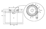
FIG. 11 shows box 54 of FIG. 10 in greater detail. In particular, an enlarged cross section and a corresponding plan view of a conductive cap 46 is depicted, wherein the cross section is taken along the A-A line of the plan view. As discussed above, the cap is formed such that a metal density of the cap is reduced, which may help to reduce stresses on the interface between the conductive cap 46 and the dielectric layer 52 in which the conductive cap 46 is disposed, thereby increasing reliability of the package. Accordingly, conductive cap 46 is formed with a section 60 (outlined by dotted lines in the plan view of conductive cap 46 of FIG. 11), including a plurality of holes in the section 60, resulting in a lower metal density of conductive cap 46 than would have occurred absent the plurality of holes 56.
In some embodiments, conductive cap 46 is disposed over TV 33 and has a width A that is greater than the width B of TV 33. In some embodiments, width A is about 10 μm to about 50 μm greater than width B. Width B, in turn, is between about 100 to about 300 μm. Conductive cap 46 is further disposed over and contacting via connection 48, which electrically couples conductive cap 46 to TV 33. In some embodiments, via connection 48 has a width C which is between about 10 to about 150 μm. In some embodiments, via connection 48 may be merged with conductive cap 46 and there may or may not be a distinguishable interface between conductive cap 46 and via connection 48.
Conductive cap 46 has a section 60 which is depicted using the dotted lines of the plan view of FIG. 11. In some embodiments, section 60 forms a ring disposed over the perimeter 58 of TV 33. In some embodiments, section 60 extends a distance D on either side of the perimeter 58 of TV 33. In some embodiments, distance D is about 5 μm to about 25 μm. Section 60 has a plurality of holes 56, about 10 μm to about 50 μm in width. Holes 56 create a lower metal density in section 60 compared to what the density of conductive cap 46 would have been without holes 56. The reduced metal density of cap 46 created by holes 56 may help to reduce the stresses on the interface between conductive cap 46 and dielectric layer 52, which may help to reduce cracking of surrounding metal connections and increase reliability of the package, particularly during thermal cycling. In some embodiments, the metal density of conductive cap 46 may be about 50 to 70 percent of the density of the conductive cap 46 if it were formed without any holes 56.
In some embodiments, holes 56 are located from about 5 μm to about 30 μm from each other and about 5 μm to about 10 μm from the edge of conductive cap 46. It may be desirable for section 60 to have as many holes 56 as possible given design limits. Holes 56 may be formed using the same materials and procedures discussed above. For example, after dielectric layer 50 is deposited and patterned, another mask layer may be deposited and patterned in such a way that, after an electroplating is done and the mask layer is removed, holes 56 are formed in conductive caps 46 due to removal of the mask layer.
Referring to FIG. 12, in some embodiments, additional RDLs 43 may be formed. The additional RDLs may be formed using similar processes and materials as described above with reference to other RDLs. FIG. 12 illustrates two layers of RDLs, while there may be one or more than two layers of RDLs 43, depending on the routing requirement of the respective package.
FIG. 13 illustrates an under bump metallization (UBM) 70 formed and patterned over an uppermost metallization pattern in accordance with some embodiments, thereby forming an electrical connection with an uppermost metallization layer, e.g., the contact pads 66 in the embodiment illustrated in FIG. 13. The UBM 70 may include a via 48 as illustrated in FIG. 13. The UBM 70 provides an electrical connection upon which an electrical connector, e.g., a solder ball/bump, a conductive pillar, or the like, may be placed. In an embodiment, the under bump metallization 70 includes a diffusion barrier layer, a seed layer, or a combination thereof. The diffusion barrier layer may include Ti, TiN, Ta, TaN, or combinations thereof. The seed layer may include copper or copper alloys. However, other metals, such as nickel, palladium, silver, gold, aluminum, combinations thereof, and multi-layers thereof, may also be included. In an embodiment, under bump metallization 70 is formed using sputtering. In other embodiments, electro plating may be used.
Connectors 68 are formed over the under bump metallization 70 in accordance with some embodiments. The connectors 68 may be solder balls, metal pillars, controlled collapse chip connection (C4) bumps, micro bumps, electroless nickel-electroless palladium-immersion gold technique (ENEPIG) formed bumps, combination thereof (e.g., a metal pillar having a solder ball attached thereof), or the like. The connectors 68 may include a conductive material such as solder, copper, aluminum, gold, nickel, silver, palladium, tin, the like, or a combination thereof. In some embodiments, the connectors 68 comprise a eutectic material and may comprise a solder bump or a solder ball, as examples. The solder material may be, for example, lead-based and lead-free solders, such as Pb—Sn compositions for lead-based solder; lead-free solders including InSb; tin, silver, and copper (SAC) compositions; and other eutectic materials that have a common melting point and form conductive solder connections in electrical applications. For lead-free solder, SAC solders of varying compositions may be used, such as SAC 105 (Sn 98.5%, Ag 1.0%, Cu 0.5%), SAC 305, and SAC 405, as examples. Lead-free connectors such as solder balls may be formed from SnCu compounds as well, without the use of silver (Ag). Alternatively, lead-free solder connectors may include tin and silver, Sn—Ag, without the use of copper. The connectors 68 may form a grid, such as a ball grid array (BGA). In some embodiments, a reflow process may be performed, giving the connectors 68 a shape of a partial sphere in some embodiments. Alternatively, the connectors 68 may comprise other shapes. The connectors 68 may also comprise non-spherical conductive connectors, for example.
In some embodiments, the connectors 68 comprise metal pillars (such as a copper pillar) formed by a sputtering, printing, electro plating, electroless plating, CVD, or the like, with or without a solder material thereon. The metal pillars may be solder free and have substantially vertical sidewalls or tapered sidewalls.
Next, carrier substrate 20 is de-bonded from the package. Release layer 22 is also cleaned from the package. The resulting structure is shown in FIG. 14. As a result of the removal of release layer 22, buffer layer 24 is exposed. Next, referring to FIG. 15, a laser drilling and an etch step are performed to expose metal features 32 through buffer layer 24 and the remaining portions of seed layer 26. A laser drilling process exposes the metal features 32. An etch step is performed in the openings to remove exposed portions of buffer layer 24 and seed layer 26. The etch step may be done using an acceptable etching process, such as by wet or dry etching. Next, the package is sawed into a plurality of packages 74. The resulting package is shown in FIG. 15.
FIG. 16 illustrates the bonding of top package 76 to TV package 74, wherein the bonding may be through solder regions 78. In some embodiments, top package 76 includes dies 80 bonded to package substrate 82. Dies 80 may include a memory die(s), which may be, for example, a Static Random Access Memory (SRAM) die, a Dynamic Random Access Memory (DRAM) die, or the like.
Other embodiments of the invention described herein are possible. FIG. 17 depicts an enlarged cross section and a corresponding plan view of conductive cap 46 in accordance with some embodiments of the invention. As discussed above, the conductive cap 46 is formed such that a metal density of the cap is reduced, which may help to reduce stresses on the interface between the conductive cap 46 and the dielectric layer 52 in which the conductive cap 46 is disposed, thereby increasing reliability of the package. Accordingly, conductive cap 46 is formed with a section 60 (outlined by dotted lines in the plan view of conductive cap 46 of FIG. 11), containing a plurality of holes in the section 60, resulting in a lower metal density of the conductive cap 46 compared to the density the cap would have had if it had been formed without the plurality of holes.
FIG. 17 depicts conductive cap 46 of some embodiments, formed in dielectric layer 52 and disposed over TV 33. Conductive cap 46 is coupled to TV 33 through via connection 48, which is formed in dielectric layer 50 and also disposed over TV 33. In some embodiments, conductive cap 46 has a width A that is greater than the width B of TV 33. In some embodiments, width A is about 10 μm to about 50 μm greater than width B, and width B is between about 100 μm to about 300 μm. The conductive cap extends a distance E beyond the perimeter 58 of TV 33. In some embodiments, distance E is about 5 μm to about 25 μm. Via connection 48 has a width C which is between about 10 μm to about 150 μm. In accordance with some embodiments, via connection 48 may be merged with conductive cap 46 and there may or may not be a distinguishable interface between conductive cap 46 and via connection 48.
In some embodiments, conductive cap 46 has a section 60 that forms a ring disposed between the perimeter 58 of TV 33 and the perimeter 84 of via connection 48. Section 60 has a plurality of holes 56, about 10 μm to about 50 μm in width, which may be formed using methods described earlier. Holes 56 result in a lower metal density of the conductive cap. In some embodiments, the inner edge of section 60 is located a distance G from the outer edge of via connection 48. In some embodiments, G is between about 10 μm to about 15 μm. The outer edge of section 60 is located a distance F from the outer perimeter 58 of TV 33. In some embodiments, F is between about 5 μm to about 25 μm. As described above in connection with other embodiments, holes 56 are located about 5 μm to about 30 μm from each other. It may be advantageous to locate as many holes 56 as possible in section 60, given design limitations. In some embodiments, the metal density of conductive cap 46 may be about 50 to 70 percent of the metal density that the cap would have had without the plurality of holes 56.
Although FIG. 11 and FIG. 17 depict different embodiments of conductive cap 46, it is possible and may be advantageous to combine both embodiments in a single conductive cap 46 with a plurality of sections 60 each containing a plurality of holes 56.
FIG. 18 depicts an enlarged cross section and a corresponding plan view of conductive cap 46 of some embodiments of conductive cap 46. As discussed above, the cap is formed such that a metal density of the cap is reduced, which may help to reduce stresses on the interfaces between the conductive cap 46 and the dielectric layer 52 in which the conductive cap 46 is disposed, thereby increasing reliability of the package. Accordingly, conductive cap 46 is formed in two pieces, a center piece 88 and a perimeter piece 90 which are physically separate from each other. It is believed that the physical separation between the center piece 88 and the perimeter piece 90 reduces the stresses between the interface of conductive cap 46 and the dielectric layer in which it is disposed, which may help to reduce cracking of surrounding metal connections and increase reliability of the package, particularly during thermal cycling.
As shown in FIG. 18, conductive cap 46 is formed in dielectric layer 52. Center piece 88 is disposed over TV 33 and electrically coupled to TV 33 through via connection 48, which is formed in dielectric layer 50 and is also disposed over TV 33. In some embodiments, TV 33 has a width B, which is between about 100 μm to about 250 μm. Via connection 48 has a width C, which is between about 10 μm to about 50 μm. Center piece 88 has a width H, which in some embodiments is between about 70 μm to about 100 μm. In accordance with some embodiments, via connection 48 may be merged with center piece 88 and there may or may not be a distinguishable interface between center piece 88 and via connection 48.
Perimeter piece 90 forms a ring disposed over the perimeter of TV 33 with opening 92 in one side of the ring. Perimeter piece 90 extends a distance K on either side of perimeter 58 TV 33. Opening 92 has a width L of about 15 μm to about 70 μm and may be about 30 μm. Center piece 88 is connected to conductive line 44, which in some embodiments extends through the opening 92 of perimeter piece 90 for connection to center piece 88. In some embodiments, conductive line 44 has a width M between about 5 μm to about 40 μm. Conductive line 44 is spaced a distance N from each side of perimeter piece 90 when passing through opening 92. Distance N is between about 5 μm to about 15 μm in some embodiments.
In some embodiments, center piece 88 may be used for signals and perimeter piece 90 may be connected to ground. In some embodiments, conductive caps 46 as depicted in FIGS. 11 and 17 may be used for connections to power sources or ground sources, while conductive caps 46 depicted in FIG. 18 may be used for signal connection. Other alternative uses for each embodiment are possible.
FIG. 19 depicts an embodiment of package 74. In some embodiments, via connections 48, conductive caps 46, and RDLs 43 are formed on both sides of TVs 33. To create this embodiment, after carrier substrate 20 is de-bonded (shown in FIG. 14), conductive caps 46, RDLs 43 and via connections 48 are formed on the other side of TVs 33 using the same methods described earlier. Additional dielectric layers and RDLs may be formed as needed for the particular circuit design. In some embodiments, the backside RDLs may be formed using similar processes and materials as discussed above on the carrier substrate 20 prior to forming TVs 33. Openings 100 may be created in the uppermost dielectric layer for electrical connection to a top layer of RDL, using any suitable laser drilling and etching process described earlier.
In some embodiments, a method of manufacturing a semiconductor device is provided. The method includes forming a through via on a substrate, the through via extending through a molding compound. A via connection is formed, disposed over and contacting the through via. A cap is then formed, disposed over and contacting the via connection, such that a width of the cap is greater than a width of the through via and a plurality of holes are formed in a first section of the cap.
In some embodiments, a method of manufacturing a semiconductor device is provided. The method includes forming a through via on a substrate, the through via extending through a molding compound. A via connection is formed, disposed over and contacting the through via. A cap is formed over the through via, including a perimeter piece and a center piece. The perimeter piece is electrically disconnected from the center piece. The center piece is disposed over and contacts the via connection.
In some embodiments, a semiconductor device is provided. The semiconductor device includes a through via extending through a molding compound. A via connection is disposed over the through via. A cap is also disposed over the through via, and contacts the via connection, wherein a width of the cap is greater than a width of the through via. A plurality of holes are formed in a first section of the cap.
Although the embodiments and their advantages have been described in detail, it should be understood that various changes, substitutions and alterations can be made herein without departing from the spirit and scope of the embodiments as defined by the appended claims. Moreover, the scope of the present application is not intended to be limited to the particular embodiments of the process, machine, manufacture, and composition of matter, means, methods and steps described in the specification. As one of ordinary skill in the art will readily appreciate from the disclosure, processes, machines, manufacture, compositions of matter, means, methods, or steps, presently existing or later to be developed, that perform substantially the same function or achieve substantially the same result as the corresponding embodiments described herein may be utilized according to the disclosure. Accordingly, the appended claims are intended to include within their scope such processes, machines, manufacture, compositions of matter, means, methods, or steps. In addition, each claim constitutes a separate embodiment, and the combination of various claims and embodiments are within the scope of the disclosure.

Claims (20)

What is claimed is:
1. A method of forming a semiconductor device, the method comprising:
forming a through via on a substrate, the through via extending through a molding compound;
forming a via connection disposed over and contacting the through via; and
forming a cap disposed over the through via and contacting the via connection, wherein a width of the cap is greater than a width of the through via, a line extends from a first portion of a perimeter of the cap, through a center point of the cap, to a second portion of the perimeter of the cap, the first portion being opposite to the second portion, the line extending a first distance from the center point of the cap to the first portion of the perimeter of the cap, the line extending a second distance from the center point of the cap to the second portion of the perimeter of the cap, the first distance and the second distance being the same, the center point of the cap overlying a center point of the through via, wherein a plurality of holes are formed in a first section of the cap, wherein a first hole of the plurality of holes comprises a perimeter, and a portion of the perimeter of the first hole that is closest to the via connection is laterally positioned between a perimeter of the through via and the first portion of the perimeter of the cap.
2. The method of claim 1, wherein the first section forms a ring disposed over the perimeter of the through via in a plan view.
3. The method of claim 2, wherein the first section extends at least 5 μm on either side of the perimeter of the through via.
4. The method of claim 1, wherein a metal density of the cap is 50 to 70 percent of a metal density that the cap would have had without the plurality of holes.
5. The method of claim 1, further comprising:
placing a die over the substrate;
forming a molding compound over the die;
planarizing the molding compound to expose a metal pillar of the die; and
forming one or more redistribution layers overlying the molding compound and electrically coupled to the cap and the metal pillar.
6. The method of claim 1, wherein the via connection has a width between 10 μm to 150 μm.
7. The method of claim 1, wherein the holes have a width of 10 μm to 50 μm.
8. The method according to claim 1, wherein the first hole exposes a dielectric layer that extends along sidewalls of the via connection.
9. The method according to claim 1, wherein a second hole of the plurality of holes comprises a perimeter, and the perimeter of the second hole is laterally positioned between the perimeter of the through via and a perimeter of the via connection.
10. A semiconductor device comprising:
a through via extending through a molding compound;
a via connection disposed over the through via; and
a cap disposed over the through via and contacting the via connection, wherein a width of the cap is greater than a width of the through via, and wherein a plurality of holes are formed in a first section of the cap, wherein a first hole of the plurality of holes comprises a perimeter, a first portion and a second portion of the perimeter of the first hole are laterally positioned between a perimeter of the through via and a perimeter of the via connection, the first portion being a portion of the perimeter that is closest to the via connection, the second portion being a portion of the perimeter that is farthest from the via connection.
11. The semiconductor device of claim 10, further comprising:
a plurality of redistribution layers over the molding compound; and
a second semiconductor device bonded to the redistribution layers.
12. The semiconductor device of claim 10, further comprising:
a die, the molding compound extending along sidewalls of the die; and
one or more redistribution layers overlying the molding compound and the die.
13. The semiconductor device of claim 10, wherein the first section forms a ring disposed between the perimeter of the through via and the perimeter of the via connection in a plan view.
14. The semiconductor device of claim 10, wherein the perimeter of the first hole is disposed over a dielectric layer, the via connection extending through the dielectric layer.
15. A method, comprising:
forming a through via on a substrate;
placing a die on the substrate;
encapsulating sidewalls of the through via and the die with a molding material;
forming a dielectric layer over the molding material;
forming a via connection in the dielectric layer, the via connection contacting the through via; and
forming a conductive cap over the via connection, wherein a plurality of holes are formed in the conductive cap, the holes overlying the dielectric layer, and wherein the conductive cap includes a perimeter, a first portion of the perimeter of the conductive cap is opposite to a second portion of the perimeter of the conductive cap, a first line that extends from the first portion of the perimeter of the conductive cap to the substrate extends through the molding material, a second line that extends from the second portion of the perimeter of the conductive cap to the substrate extends through the molding material, and the first line and the second line are perpendicular to a surface of the molding material, and wherein a center point of the conductive cap overlies a center point of the via connection, the center point of the conductive cap is between the first portion of the perimeter and the second portion of the perimeter, the first portion of the perimeter is a first distance from the center point of the conductive cap, the second portion is a second distance from the center point of the conductive cap, and the first distance and the second distance are the same, and wherein a hole of the plurality of holes is disposed between the first portion of the perimeter of the conductive cap and a perimeter of the via connection.
16. The method of claim 15, wherein the holes are formed in a first section of the conductive cap, and the first section has an annular shape.
17. The method of claim 16, wherein the first section is disposed over a perimeter of the through via.
18. The method of claim 16, wherein the first section is disposed over the dielectric layer between a perimeter of the through via and a perimeter of the via connection.
19. The method of claim 18, wherein the first section is offset in a plan view from the perimeter of the through via and the perimeter of the via connection.
20. The method of claim 15, wherein the through via and the conductive cap have circular shapes in a plan view.
US14/871,593 2015-09-30 2015-09-30 Integrated fan-out structure and method of forming Active US10068844B2 (en)

Priority Applications (3)

Application Number Priority Date Filing Date Title
US14/871,593 US10068844B2 (en) 2015-09-30 2015-09-30 Integrated fan-out structure and method of forming
CN201610751428.9A CN106558537B (en) 2015-09-30 2016-08-29 Integrated multi-output structure and forming method
TW105129275A TWI702688B (en) 2015-09-30 2016-09-09 Integrated fan-out structure and method of forming

Applications Claiming Priority (1)

Application Number Priority Date Filing Date Title
US14/871,593 US10068844B2 (en) 2015-09-30 2015-09-30 Integrated fan-out structure and method of forming

Publications (2)

Publication Number Publication Date
US20170092581A1 US20170092581A1 (en) 2017-03-30
US10068844B2 true US10068844B2 (en) 2018-09-04

Family

ID=58406692

Family Applications (1)

Application Number Title Priority Date Filing Date
US14/871,593 Active US10068844B2 (en) 2015-09-30 2015-09-30 Integrated fan-out structure and method of forming

Country Status (3)

Country Link
US (1) US10068844B2 (en)
CN (1) CN106558537B (en)
TW (1) TWI702688B (en)

Cited By (7)

* Cited by examiner, † Cited by third party
Publication number Priority date Publication date Assignee Title
US10290584B2 (en) * 2017-05-31 2019-05-14 Taiwan Semiconductor Manufacturing Company, Ltd. Conductive vias in semiconductor packages and methods of forming same
US10586763B2 (en) 2017-11-15 2020-03-10 Taiwan Semiconductor Manufacturing Company, Ltd. Semiconductor device and method of manufacture
US11205615B2 (en) 2017-11-15 2021-12-21 Taiwan Semiconductor Manufacturing Company, Ltd. Semiconductor device and method of manufacture
US11342274B2 (en) 2020-01-23 2022-05-24 Samsung Electronics Co., Ltd. Semiconductor package
KR20220106653A (en) * 2021-01-22 2022-07-29 타이완 세미콘덕터 매뉴팩쳐링 컴퍼니 리미티드 Semiconductor packaging and methods of forming same
US11784129B2 (en) 2020-08-07 2023-10-10 Samsung Electronics Co., Ltd. Semiconductor package and method of fabricating the same
US11894310B2 (en) 2020-07-29 2024-02-06 Samsung Electronics Co., Ltd. Fan-out semiconductor package

Families Citing this family (12)

* Cited by examiner, † Cited by third party
Publication number Priority date Publication date Assignee Title
JP2016192447A (en) * 2015-03-30 2016-11-10 株式会社東芝 Semiconductor device
DE102017102035A1 (en) * 2017-02-02 2018-08-02 Infineon Technologies Ag A semiconductor device, method of manufacturing a semiconductor device, and method of amplifying a die in a semiconductor device
DE102018108924B4 (en) * 2017-06-30 2025-04-30 Taiwan Semiconductor Manufacturing Company, Ltd. Method for producing a semiconductor package
US10636757B2 (en) * 2017-08-29 2020-04-28 Taiwan Semiconductor Manufacturing Co., Ltd. Integrated circuit component package and method of fabricating the same
TWI641096B (en) * 2017-11-10 2018-11-11 旺宏電子股份有限公司 Contact hole structure mrthod for fabricting the same and applications thereof
KR102061852B1 (en) * 2017-12-18 2020-01-02 삼성전자주식회사 Semiconductor package
US12100682B2 (en) * 2018-07-15 2024-09-24 Taiwan Semiconductor Manufacturing Company, Ltd. Package structure with conductive patterns in a redistribution layer
KR102798785B1 (en) * 2019-03-20 2025-04-23 삼성전자주식회사 Method of manufacturing semiconductor device
US11600590B2 (en) * 2019-03-22 2023-03-07 Advanced Semiconductor Engineering, Inc. Semiconductor device and semiconductor package
US11756870B2 (en) * 2021-04-29 2023-09-12 Taiwan Semiconductor Manufacturing Company, Ltd. Stacked via structure disposed on a conductive pillar of a semiconductor die
CN113451161B (en) * 2021-06-29 2023-08-25 矽磐微电子(重庆)有限公司 Semiconductor packaging method and semiconductor packaging structure
KR20240023343A (en) * 2022-08-12 2024-02-21 삼성전자주식회사 Semiconductor package

Citations (25)

* Cited by examiner, † Cited by third party
Publication number Priority date Publication date Assignee Title
US20040177999A1 (en) * 2003-02-28 2004-09-16 Ngk Spark Plug Co., Ltd. Wiring substrate
US20110291288A1 (en) 2010-05-26 2011-12-01 Taiwan Semiconductor Manufacturing Company, Ltd. Package systems having interposers
US8361842B2 (en) 2010-07-30 2013-01-29 Taiwan Semiconductor Manufacturing Company, Ltd. Embedded wafer-level bonding approaches
US20130026468A1 (en) 2010-04-07 2013-01-31 Shimadzu Corporation Radiation detector and method of manufacturing the same
US20130062760A1 (en) 2010-10-14 2013-03-14 Taiwan Semiconductor Manufacturing Company, Ltd. Packaging Methods and Structures Using a Die Attach Film
US20130062761A1 (en) 2011-09-09 2013-03-14 Taiwan Semiconductor Manufacturing Company, Ltd. Packaging Methods and Structures for Semiconductor Devices
US20130168848A1 (en) 2011-12-28 2013-07-04 Taiwan Semiconductor Manufacturing Company, Ltd. Packaged semiconductor device and method of packaging the semiconductor device
US20130307140A1 (en) 2012-05-18 2013-11-21 Taiwan Semiconductor Manufacturing Company, Ltd. Packaging with interposer frame
US20140077356A1 (en) * 2012-09-14 2014-03-20 Taiwan Semiconductor Manufacturing Company, Ltd. Post Passivation Interconnect Structures and Methods for Forming the Same
US8680647B2 (en) 2011-12-29 2014-03-25 Taiwan Semiconductor Manufacturing Company, Ltd. Packages with passive devices and methods of forming the same
US8703542B2 (en) 2012-05-18 2014-04-22 Taiwan Semiconductor Manufacturing Company, Ltd. Wafer-level packaging mechanisms
US20140131858A1 (en) * 2012-11-14 2014-05-15 Taiwan Semiconductor Manufacturing Company, Ltd. Warpage Control of Semiconductor Die Package
US8759964B2 (en) 2007-07-17 2014-06-24 Taiwan Semiconductor Manufacturing Company, Ltd. Wafer level package structure and fabrication methods
US8778738B1 (en) 2013-02-19 2014-07-15 Taiwan Semiconductor Manufacturing Company, Ltd. Packaged semiconductor devices and packaging devices and methods
US8785299B2 (en) 2012-11-30 2014-07-22 Taiwan Semiconductor Manufacturing Company, Ltd. Package with a fan-out structure and method of forming the same
US20140203429A1 (en) 2013-01-18 2014-07-24 Taiwan Semiconductor Manufacturing Company, Ltd. Fan-out package structure and methods for forming the same
US20140225222A1 (en) 2013-02-11 2014-08-14 Taiwan Semiconductor Manufacturing Company, Ltd. Package with metal-insulator-metal capacitor and method of manufacturing the same
US8809996B2 (en) 2012-06-29 2014-08-19 Taiwan Semiconductor Manufacturing Company, Ltd. Package with passive devices and method of forming the same
US8829676B2 (en) 2011-06-28 2014-09-09 Taiwan Semiconductor Manufacturing Company, Ltd. Interconnect structure for wafer level package
US20140252646A1 (en) 2013-03-06 2014-09-11 Taiwan Semiconductor Manufacturing Company, Ltd. Interconnect Structure for Package-on-Package Devices
US20140264930A1 (en) 2013-03-15 2014-09-18 Taiwan Semiconductor Manufacturing Company, Ltd. Fan-Out Interconnect Structure and Method for Forming Same
US8877554B2 (en) 2013-03-15 2014-11-04 Taiwan Semiconductor Manufacturing Company, Ltd. Packaged semiconductor devices, methods of packaging semiconductor devices, and PoP devices
US20150108635A1 (en) * 2013-10-23 2015-04-23 Taiwan Semiconductor Manufacturing Company Ltd. Semiconductor structure and manufacturing method thereof
US20160284639A1 (en) * 2015-03-27 2016-09-29 Chipmos Technologies Inc Semiconductor structure
US20160351499A1 (en) * 2015-05-25 2016-12-01 Fujitsu Limited Semiconductor device and electronic device

Family Cites Families (4)

* Cited by examiner, † Cited by third party
Publication number Priority date Publication date Assignee Title
US7405147B2 (en) * 2004-01-30 2008-07-29 International Business Machines Corporation Device and methodology for reducing effective dielectric constant in semiconductor devices
TWI505473B (en) * 2005-01-28 2015-10-21 半導體能源研究所股份有限公司 Semiconductor device, electronic device, and method of manufacturing semiconductor device
KR100620810B1 (en) * 2005-03-07 2006-09-07 삼성전자주식회사 MEMS device package and manufacturing method thereof
US8884400B2 (en) * 2012-12-27 2014-11-11 Taiwan Semiconductor Manufacturing Company, Ltd. Capacitor in Post-Passivation structures and methods of forming the same

Patent Citations (26)

* Cited by examiner, † Cited by third party
Publication number Priority date Publication date Assignee Title
US20040177999A1 (en) * 2003-02-28 2004-09-16 Ngk Spark Plug Co., Ltd. Wiring substrate
US8759964B2 (en) 2007-07-17 2014-06-24 Taiwan Semiconductor Manufacturing Company, Ltd. Wafer level package structure and fabrication methods
US20130026468A1 (en) 2010-04-07 2013-01-31 Shimadzu Corporation Radiation detector and method of manufacturing the same
US20110291288A1 (en) 2010-05-26 2011-12-01 Taiwan Semiconductor Manufacturing Company, Ltd. Package systems having interposers
US8361842B2 (en) 2010-07-30 2013-01-29 Taiwan Semiconductor Manufacturing Company, Ltd. Embedded wafer-level bonding approaches
US20130062760A1 (en) 2010-10-14 2013-03-14 Taiwan Semiconductor Manufacturing Company, Ltd. Packaging Methods and Structures Using a Die Attach Film
US8829676B2 (en) 2011-06-28 2014-09-09 Taiwan Semiconductor Manufacturing Company, Ltd. Interconnect structure for wafer level package
US20130062761A1 (en) 2011-09-09 2013-03-14 Taiwan Semiconductor Manufacturing Company, Ltd. Packaging Methods and Structures for Semiconductor Devices
US20130168848A1 (en) 2011-12-28 2013-07-04 Taiwan Semiconductor Manufacturing Company, Ltd. Packaged semiconductor device and method of packaging the semiconductor device
US8680647B2 (en) 2011-12-29 2014-03-25 Taiwan Semiconductor Manufacturing Company, Ltd. Packages with passive devices and methods of forming the same
US20130307140A1 (en) 2012-05-18 2013-11-21 Taiwan Semiconductor Manufacturing Company, Ltd. Packaging with interposer frame
US8703542B2 (en) 2012-05-18 2014-04-22 Taiwan Semiconductor Manufacturing Company, Ltd. Wafer-level packaging mechanisms
US8809996B2 (en) 2012-06-29 2014-08-19 Taiwan Semiconductor Manufacturing Company, Ltd. Package with passive devices and method of forming the same
US20140077356A1 (en) * 2012-09-14 2014-03-20 Taiwan Semiconductor Manufacturing Company, Ltd. Post Passivation Interconnect Structures and Methods for Forming the Same
US20140131858A1 (en) * 2012-11-14 2014-05-15 Taiwan Semiconductor Manufacturing Company, Ltd. Warpage Control of Semiconductor Die Package
US8785299B2 (en) 2012-11-30 2014-07-22 Taiwan Semiconductor Manufacturing Company, Ltd. Package with a fan-out structure and method of forming the same
US20140203429A1 (en) 2013-01-18 2014-07-24 Taiwan Semiconductor Manufacturing Company, Ltd. Fan-out package structure and methods for forming the same
US8803306B1 (en) 2013-01-18 2014-08-12 Taiwan Semiconductor Manufacturing Company, Ltd. Fan-out package structure and methods for forming the same
US20140225222A1 (en) 2013-02-11 2014-08-14 Taiwan Semiconductor Manufacturing Company, Ltd. Package with metal-insulator-metal capacitor and method of manufacturing the same
US8778738B1 (en) 2013-02-19 2014-07-15 Taiwan Semiconductor Manufacturing Company, Ltd. Packaged semiconductor devices and packaging devices and methods
US20140252646A1 (en) 2013-03-06 2014-09-11 Taiwan Semiconductor Manufacturing Company, Ltd. Interconnect Structure for Package-on-Package Devices
US20140264930A1 (en) 2013-03-15 2014-09-18 Taiwan Semiconductor Manufacturing Company, Ltd. Fan-Out Interconnect Structure and Method for Forming Same
US8877554B2 (en) 2013-03-15 2014-11-04 Taiwan Semiconductor Manufacturing Company, Ltd. Packaged semiconductor devices, methods of packaging semiconductor devices, and PoP devices
US20150108635A1 (en) * 2013-10-23 2015-04-23 Taiwan Semiconductor Manufacturing Company Ltd. Semiconductor structure and manufacturing method thereof
US20160284639A1 (en) * 2015-03-27 2016-09-29 Chipmos Technologies Inc Semiconductor structure
US20160351499A1 (en) * 2015-05-25 2016-12-01 Fujitsu Limited Semiconductor device and electronic device

Cited By (13)

* Cited by examiner, † Cited by third party
Publication number Priority date Publication date Assignee Title
US10290584B2 (en) * 2017-05-31 2019-05-14 Taiwan Semiconductor Manufacturing Company, Ltd. Conductive vias in semiconductor packages and methods of forming same
US10629537B2 (en) 2017-05-31 2020-04-21 Taiwan Semiconductor Manufacturing Company, Ltd. Conductive vias in semiconductor packages and methods of forming same
US10586763B2 (en) 2017-11-15 2020-03-10 Taiwan Semiconductor Manufacturing Company, Ltd. Semiconductor device and method of manufacture
US11205615B2 (en) 2017-11-15 2021-12-21 Taiwan Semiconductor Manufacturing Company, Ltd. Semiconductor device and method of manufacture
US11342274B2 (en) 2020-01-23 2022-05-24 Samsung Electronics Co., Ltd. Semiconductor package
US11942434B2 (en) 2020-01-23 2024-03-26 Samsung Electronics Co., Ltd. Method of manufacturing a semiconductor package
US11894310B2 (en) 2020-07-29 2024-02-06 Samsung Electronics Co., Ltd. Fan-out semiconductor package
US11784129B2 (en) 2020-08-07 2023-10-10 Samsung Electronics Co., Ltd. Semiconductor package and method of fabricating the same
US12334445B2 (en) 2020-08-07 2025-06-17 Samsung Electronics Co., Ltd. Method of fabricating a semiconductor package
US11728312B2 (en) 2021-01-22 2023-08-15 Taiwan Semiconductor Manufacturing Co., Ltd. Semiconductor packaging and methods of forming same
KR102557597B1 (en) 2021-01-22 2023-07-19 타이완 세미콘덕터 매뉴팩쳐링 컴퍼니 리미티드 Semiconductor packaging and methods of forming same
KR20220106653A (en) * 2021-01-22 2022-07-29 타이완 세미콘덕터 매뉴팩쳐링 컴퍼니 리미티드 Semiconductor packaging and methods of forming same
US12482787B2 (en) 2021-01-22 2025-11-25 Taiwan Semiconductor Manufacturing Co., Ltd. Semiconductor packaging and methods of forming same

Also Published As

Publication number Publication date
TW201724357A (en) 2017-07-01
CN106558537A (en) 2017-04-05
TWI702688B (en) 2020-08-21
CN106558537B (en) 2021-11-09
US20170092581A1 (en) 2017-03-30

Similar Documents

Publication Publication Date Title
US11276656B2 (en) Integrated fan-out structure and method of forming
US12224247B2 (en) Fan-out package having a main die and a dummy die
US10068844B2 (en) Integrated fan-out structure and method of forming
US20220246581A1 (en) Stacked Integrated Circuit Structure and Method of Forming
US11721559B2 (en) Integrated circuit package pad and methods of forming
US10049986B2 (en) Package structures and methods of making the same
TWI550787B (en) Ring structure in grains
US11133197B2 (en) Semiconductor structure and method of forming

Legal Events

Date Code Title Description
AS Assignment

Owner name: TAIWAN SEMICONDUCTOR MANUFACTURING COMPANY, LTD.,

Free format text: ASSIGNMENT OF ASSIGNORS INTEREST;ASSIGNORS:CHIU, MING-YEN;CHEN, HSEIN-WEI;REEL/FRAME:036825/0540

Effective date: 20150930

STCF Information on status: patent grant

Free format text: PATENTED CASE

MAFP Maintenance fee payment

Free format text: PAYMENT OF MAINTENANCE FEE, 4TH YEAR, LARGE ENTITY (ORIGINAL EVENT CODE: M1551); ENTITY STATUS OF PATENT OWNER: LARGE ENTITY

Year of fee payment: 4

MAFP Maintenance fee payment

Free format text: PAYMENT OF MAINTENANCE FEE, 8TH YEAR, LARGE ENTITY (ORIGINAL EVENT CODE: M1552); ENTITY STATUS OF PATENT OWNER: LARGE ENTITY

Year of fee payment: 8