US10043801B2 - Air gap spacer for metal gates - Google Patents
Air gap spacer for metal gates Download PDFInfo
- Publication number
- US10043801B2 US10043801B2 US15/786,828 US201715786828A US10043801B2 US 10043801 B2 US10043801 B2 US 10043801B2 US 201715786828 A US201715786828 A US 201715786828A US 10043801 B2 US10043801 B2 US 10043801B2
- Authority
- US
- United States
- Prior art keywords
- forming
- trench
- gate
- sacrificial spacer
- spacer
- Prior art date
- Legal status (The legal status is an assumption and is not a legal conclusion. Google has not performed a legal analysis and makes no representation as to the accuracy of the status listed.)
- Active
Links
- 125000006850 spacer group Chemical group 0.000 title claims abstract description 129
- 229910052751 metal Inorganic materials 0.000 title claims abstract description 110
- 239000002184 metal Substances 0.000 title claims abstract description 110
- 239000003989 dielectric material Substances 0.000 claims abstract description 62
- 238000000034 method Methods 0.000 claims abstract description 47
- 239000000463 material Substances 0.000 claims description 119
- 239000010410 layer Substances 0.000 claims description 63
- 238000005530 etching Methods 0.000 claims description 13
- 239000011229 interlayer Substances 0.000 claims description 12
- 238000005229 chemical vapour deposition Methods 0.000 claims description 11
- 238000000151 deposition Methods 0.000 claims description 6
- 238000000137 annealing Methods 0.000 claims description 5
- 238000004891 communication Methods 0.000 claims description 3
- 230000005669 field effect Effects 0.000 claims description 2
- 239000004065 semiconductor Substances 0.000 abstract description 24
- 238000004519 manufacturing process Methods 0.000 description 29
- 238000001465 metallisation Methods 0.000 description 22
- 239000007789 gas Substances 0.000 description 14
- 230000008569 process Effects 0.000 description 14
- VYPSYNLAJGMNEJ-UHFFFAOYSA-N Silicium dioxide Chemical compound O=[Si]=O VYPSYNLAJGMNEJ-UHFFFAOYSA-N 0.000 description 12
- XUIMIQQOPSSXEZ-UHFFFAOYSA-N Silicon Chemical compound [Si] XUIMIQQOPSSXEZ-UHFFFAOYSA-N 0.000 description 11
- 229910052710 silicon Inorganic materials 0.000 description 11
- 239000010703 silicon Substances 0.000 description 11
- 230000003071 parasitic effect Effects 0.000 description 9
- 239000007769 metal material Substances 0.000 description 7
- OKTJSMMVPCPJKN-UHFFFAOYSA-N Carbon Chemical compound [C] OKTJSMMVPCPJKN-UHFFFAOYSA-N 0.000 description 6
- 229910000577 Silicon-germanium Inorganic materials 0.000 description 6
- 230000015572 biosynthetic process Effects 0.000 description 6
- 229910052799 carbon Inorganic materials 0.000 description 6
- 238000005755 formation reaction Methods 0.000 description 6
- 238000001020 plasma etching Methods 0.000 description 6
- BASFCYQUMIYNBI-UHFFFAOYSA-N platinum Chemical compound [Pt] BASFCYQUMIYNBI-UHFFFAOYSA-N 0.000 description 6
- 229910052732 germanium Inorganic materials 0.000 description 5
- 238000005498 polishing Methods 0.000 description 5
- 238000012545 processing Methods 0.000 description 5
- 229910052814 silicon oxide Inorganic materials 0.000 description 5
- 239000000126 substance Substances 0.000 description 5
- 229910045601 alloy Inorganic materials 0.000 description 4
- 239000000956 alloy Substances 0.000 description 4
- 239000006117 anti-reflective coating Substances 0.000 description 4
- 238000001505 atmospheric-pressure chemical vapour deposition Methods 0.000 description 4
- 239000010949 copper Substances 0.000 description 4
- GNPVGFCGXDBREM-UHFFFAOYSA-N germanium atom Chemical compound [Ge] GNPVGFCGXDBREM-UHFFFAOYSA-N 0.000 description 4
- 239000010931 gold Substances 0.000 description 4
- 238000004518 low pressure chemical vapour deposition Methods 0.000 description 4
- 239000000203 mixture Substances 0.000 description 4
- 150000004767 nitrides Chemical class 0.000 description 4
- 238000000623 plasma-assisted chemical vapour deposition Methods 0.000 description 4
- 235000012239 silicon dioxide Nutrition 0.000 description 4
- 239000000377 silicon dioxide Substances 0.000 description 4
- 239000000758 substrate Substances 0.000 description 4
- 229910052581 Si3N4 Inorganic materials 0.000 description 3
- 238000009413 insulation Methods 0.000 description 3
- 230000004048 modification Effects 0.000 description 3
- 238000012986 modification Methods 0.000 description 3
- 238000005240 physical vapour deposition Methods 0.000 description 3
- WFKWXMTUELFFGS-UHFFFAOYSA-N tungsten Chemical compound [W] WFKWXMTUELFFGS-UHFFFAOYSA-N 0.000 description 3
- 229910052721 tungsten Inorganic materials 0.000 description 3
- 239000010937 tungsten Substances 0.000 description 3
- XKRFYHLGVUSROY-UHFFFAOYSA-N Argon Chemical compound [Ar] XKRFYHLGVUSROY-UHFFFAOYSA-N 0.000 description 2
- IJGRMHOSHXDMSA-UHFFFAOYSA-N Atomic nitrogen Chemical compound N#N IJGRMHOSHXDMSA-UHFFFAOYSA-N 0.000 description 2
- RYGMFSIKBFXOCR-UHFFFAOYSA-N Copper Chemical compound [Cu] RYGMFSIKBFXOCR-UHFFFAOYSA-N 0.000 description 2
- GWEVSGVZZGPLCZ-UHFFFAOYSA-N Titan oxide Chemical compound O=[Ti]=O GWEVSGVZZGPLCZ-UHFFFAOYSA-N 0.000 description 2
- NRTOMJZYCJJWKI-UHFFFAOYSA-N Titanium nitride Chemical compound [Ti]#N NRTOMJZYCJJWKI-UHFFFAOYSA-N 0.000 description 2
- MCMNRKCIXSYSNV-UHFFFAOYSA-N Zirconium dioxide Chemical compound O=[Zr]=O MCMNRKCIXSYSNV-UHFFFAOYSA-N 0.000 description 2
- LEVVHYCKPQWKOP-UHFFFAOYSA-N [Si].[Ge] Chemical compound [Si].[Ge] LEVVHYCKPQWKOP-UHFFFAOYSA-N 0.000 description 2
- 229910052782 aluminium Inorganic materials 0.000 description 2
- XAGFODPZIPBFFR-UHFFFAOYSA-N aluminium Chemical compound [Al] XAGFODPZIPBFFR-UHFFFAOYSA-N 0.000 description 2
- 238000000231 atomic layer deposition Methods 0.000 description 2
- 239000012159 carrier gas Substances 0.000 description 2
- 239000007795 chemical reaction product Substances 0.000 description 2
- 239000011248 coating agent Substances 0.000 description 2
- 238000000576 coating method Methods 0.000 description 2
- 229910052802 copper Inorganic materials 0.000 description 2
- 238000000354 decomposition reaction Methods 0.000 description 2
- 239000011521 glass Substances 0.000 description 2
- PCHJSUWPFVWCPO-UHFFFAOYSA-N gold Chemical compound [Au] PCHJSUWPFVWCPO-UHFFFAOYSA-N 0.000 description 2
- 229910052737 gold Inorganic materials 0.000 description 2
- 150000002739 metals Chemical class 0.000 description 2
- 229910052697 platinum Inorganic materials 0.000 description 2
- 229920003209 poly(hydridosilsesquioxane) Polymers 0.000 description 2
- 229910021420 polycrystalline silicon Inorganic materials 0.000 description 2
- 239000000047 product Substances 0.000 description 2
- HQVNEWCFYHHQES-UHFFFAOYSA-N silicon nitride Chemical compound N12[Si]34N5[Si]62N3[Si]51N64 HQVNEWCFYHHQES-UHFFFAOYSA-N 0.000 description 2
- 239000002002 slurry Substances 0.000 description 2
- 238000005979 thermal decomposition reaction Methods 0.000 description 2
- 239000010936 titanium Substances 0.000 description 2
- KZBUYRJDOAKODT-UHFFFAOYSA-N Chlorine Chemical compound ClCl KZBUYRJDOAKODT-UHFFFAOYSA-N 0.000 description 1
- ZAMOUSCENKQFHK-UHFFFAOYSA-N Chlorine atom Chemical compound [Cl] ZAMOUSCENKQFHK-UHFFFAOYSA-N 0.000 description 1
- YCKRFDGAMUMZLT-UHFFFAOYSA-N Fluorine atom Chemical compound [F] YCKRFDGAMUMZLT-UHFFFAOYSA-N 0.000 description 1
- VEXZGXHMUGYJMC-UHFFFAOYSA-N Hydrochloric acid Chemical compound Cl VEXZGXHMUGYJMC-UHFFFAOYSA-N 0.000 description 1
- 229910002244 LaAlO3 Inorganic materials 0.000 description 1
- BPQQTUXANYXVAA-UHFFFAOYSA-N Orthosilicate Chemical compound [O-][Si]([O-])([O-])[O-] BPQQTUXANYXVAA-UHFFFAOYSA-N 0.000 description 1
- 239000004952 Polyamide Substances 0.000 description 1
- 239000004793 Polystyrene Substances 0.000 description 1
- KJTLSVCANCCWHF-UHFFFAOYSA-N Ruthenium Chemical compound [Ru] KJTLSVCANCCWHF-UHFFFAOYSA-N 0.000 description 1
- 229910020286 SiOxNy Inorganic materials 0.000 description 1
- BLRPTPMANUNPDV-UHFFFAOYSA-N Silane Chemical compound [SiH4] BLRPTPMANUNPDV-UHFFFAOYSA-N 0.000 description 1
- BQCADISMDOOEFD-UHFFFAOYSA-N Silver Chemical compound [Ag] BQCADISMDOOEFD-UHFFFAOYSA-N 0.000 description 1
- 229910002370 SrTiO3 Inorganic materials 0.000 description 1
- RTAQQCXQSZGOHL-UHFFFAOYSA-N Titanium Chemical compound [Ti] RTAQQCXQSZGOHL-UHFFFAOYSA-N 0.000 description 1
- ZILJFRYKLPPLTO-UHFFFAOYSA-N [C].[B].[Si] Chemical compound [C].[B].[Si] ZILJFRYKLPPLTO-UHFFFAOYSA-N 0.000 description 1
- CEPICIBPGDWCRU-UHFFFAOYSA-N [Si].[Hf] Chemical compound [Si].[Hf] CEPICIBPGDWCRU-UHFFFAOYSA-N 0.000 description 1
- 230000002411 adverse Effects 0.000 description 1
- UQZIWOQVLUASCR-UHFFFAOYSA-N alumane;titanium Chemical compound [AlH3].[Ti] UQZIWOQVLUASCR-UHFFFAOYSA-N 0.000 description 1
- PNEYBMLMFCGWSK-UHFFFAOYSA-N aluminium oxide Inorganic materials [O-2].[O-2].[O-2].[Al+3].[Al+3] PNEYBMLMFCGWSK-UHFFFAOYSA-N 0.000 description 1
- 238000013459 approach Methods 0.000 description 1
- 229910052786 argon Inorganic materials 0.000 description 1
- 239000006227 byproduct Substances 0.000 description 1
- 150000001721 carbon Chemical class 0.000 description 1
- 230000015556 catabolic process Effects 0.000 description 1
- 239000000919 ceramic Substances 0.000 description 1
- 239000000460 chlorine Substances 0.000 description 1
- 229910052801 chlorine Inorganic materials 0.000 description 1
- 150000001875 compounds Chemical class 0.000 description 1
- PMHQVHHXPFUNSP-UHFFFAOYSA-M copper(1+);methylsulfanylmethane;bromide Chemical compound Br[Cu].CSC PMHQVHHXPFUNSP-UHFFFAOYSA-M 0.000 description 1
- 229910052593 corundum Inorganic materials 0.000 description 1
- 229910021419 crystalline silicon Inorganic materials 0.000 description 1
- 238000006731 degradation reaction Methods 0.000 description 1
- 230000008021 deposition Effects 0.000 description 1
- BUMGIEFFCMBQDG-UHFFFAOYSA-N dichlorosilicon Chemical compound Cl[Si]Cl BUMGIEFFCMBQDG-UHFFFAOYSA-N 0.000 description 1
- VXGHASBVNMHGDI-UHFFFAOYSA-N digermane Chemical compound [Ge][Ge] VXGHASBVNMHGDI-UHFFFAOYSA-N 0.000 description 1
- PZPGRFITIJYNEJ-UHFFFAOYSA-N disilane Chemical compound [SiH3][SiH3] PZPGRFITIJYNEJ-UHFFFAOYSA-N 0.000 description 1
- 230000000694 effects Effects 0.000 description 1
- 229910052731 fluorine Inorganic materials 0.000 description 1
- 239000011737 fluorine Substances 0.000 description 1
- 229910000078 germane Inorganic materials 0.000 description 1
- 229910052735 hafnium Inorganic materials 0.000 description 1
- VBJZVLUMGGDVMO-UHFFFAOYSA-N hafnium atom Chemical compound [Hf] VBJZVLUMGGDVMO-UHFFFAOYSA-N 0.000 description 1
- CJNBYAVZURUTKZ-UHFFFAOYSA-N hafnium(IV) oxide Inorganic materials O=[Hf]=O CJNBYAVZURUTKZ-UHFFFAOYSA-N 0.000 description 1
- 239000001257 hydrogen Substances 0.000 description 1
- 150000002431 hydrogen Chemical class 0.000 description 1
- 229910052739 hydrogen Inorganic materials 0.000 description 1
- 229910010272 inorganic material Inorganic materials 0.000 description 1
- 239000011147 inorganic material Substances 0.000 description 1
- 229910052809 inorganic oxide Inorganic materials 0.000 description 1
- 229920000592 inorganic polymer Polymers 0.000 description 1
- 239000013067 intermediate product Substances 0.000 description 1
- 238000010884 ion-beam technique Methods 0.000 description 1
- MRELNEQAGSRDBK-UHFFFAOYSA-N lanthanum oxide Inorganic materials [O-2].[O-2].[O-2].[La+3].[La+3] MRELNEQAGSRDBK-UHFFFAOYSA-N 0.000 description 1
- 238000000608 laser ablation Methods 0.000 description 1
- NFFIWVVINABMKP-UHFFFAOYSA-N methylidynetantalum Chemical compound [Ta]#C NFFIWVVINABMKP-UHFFFAOYSA-N 0.000 description 1
- 229910003465 moissanite Inorganic materials 0.000 description 1
- 229910052757 nitrogen Inorganic materials 0.000 description 1
- 229920000620 organic polymer Polymers 0.000 description 1
- KTUFCUMIWABKDW-UHFFFAOYSA-N oxo(oxolanthaniooxy)lanthanum Chemical compound O=[La]O[La]=O KTUFCUMIWABKDW-UHFFFAOYSA-N 0.000 description 1
- 239000004033 plastic Substances 0.000 description 1
- 229920003023 plastic Polymers 0.000 description 1
- 229920003229 poly(methyl methacrylate) Polymers 0.000 description 1
- 229920000636 poly(norbornene) polymer Polymers 0.000 description 1
- 229920002647 polyamide Polymers 0.000 description 1
- 229920000642 polymer Polymers 0.000 description 1
- 229920001451 polypropylene glycol Polymers 0.000 description 1
- 229920005591 polysilicon Polymers 0.000 description 1
- 229920001296 polysiloxane Polymers 0.000 description 1
- 229920002223 polystyrene Polymers 0.000 description 1
- 229910021426 porous silicon Inorganic materials 0.000 description 1
- 230000009467 reduction Effects 0.000 description 1
- 229910052707 ruthenium Inorganic materials 0.000 description 1
- 238000007789 sealing Methods 0.000 description 1
- 229910000077 silane Inorganic materials 0.000 description 1
- 229910010271 silicon carbide Inorganic materials 0.000 description 1
- 229910052709 silver Inorganic materials 0.000 description 1
- 239000004332 silver Substances 0.000 description 1
- 239000011343 solid material Substances 0.000 description 1
- 238000004544 sputter deposition Methods 0.000 description 1
- -1 such as Substances 0.000 description 1
- 229910003468 tantalcarbide Inorganic materials 0.000 description 1
- 229910052715 tantalum Inorganic materials 0.000 description 1
- GUVRBAGPIYLISA-UHFFFAOYSA-N tantalum atom Chemical compound [Ta] GUVRBAGPIYLISA-UHFFFAOYSA-N 0.000 description 1
- 229910052719 titanium Inorganic materials 0.000 description 1
- VEDJZFSRVVQBIL-UHFFFAOYSA-N trisilane Chemical compound [SiH3][SiH2][SiH3] VEDJZFSRVVQBIL-UHFFFAOYSA-N 0.000 description 1
- 229910001845 yogo sapphire Inorganic materials 0.000 description 1
- RUDFQVOCFDJEEF-UHFFFAOYSA-N yttrium(III) oxide Inorganic materials [O-2].[O-2].[O-2].[Y+3].[Y+3] RUDFQVOCFDJEEF-UHFFFAOYSA-N 0.000 description 1
Images


Classifications
-
- H—ELECTRICITY
- H01—ELECTRIC ELEMENTS
- H01L—SEMICONDUCTOR DEVICES NOT COVERED BY CLASS H10
- H01L27/00—Devices consisting of a plurality of semiconductor or other solid-state components formed in or on a common substrate
- H01L27/02—Devices consisting of a plurality of semiconductor or other solid-state components formed in or on a common substrate including semiconductor components specially adapted for rectifying, oscillating, amplifying or switching and having at least one potential-jump barrier or surface barrier; including integrated passive circuit elements with at least one potential-jump barrier or surface barrier
- H01L27/04—Devices consisting of a plurality of semiconductor or other solid-state components formed in or on a common substrate including semiconductor components specially adapted for rectifying, oscillating, amplifying or switching and having at least one potential-jump barrier or surface barrier; including integrated passive circuit elements with at least one potential-jump barrier or surface barrier the substrate being a semiconductor body
- H01L27/08—Devices consisting of a plurality of semiconductor or other solid-state components formed in or on a common substrate including semiconductor components specially adapted for rectifying, oscillating, amplifying or switching and having at least one potential-jump barrier or surface barrier; including integrated passive circuit elements with at least one potential-jump barrier or surface barrier the substrate being a semiconductor body including only semiconductor components of a single kind
- H01L27/085—Devices consisting of a plurality of semiconductor or other solid-state components formed in or on a common substrate including semiconductor components specially adapted for rectifying, oscillating, amplifying or switching and having at least one potential-jump barrier or surface barrier; including integrated passive circuit elements with at least one potential-jump barrier or surface barrier the substrate being a semiconductor body including only semiconductor components of a single kind including field-effect components only
- H01L27/088—Devices consisting of a plurality of semiconductor or other solid-state components formed in or on a common substrate including semiconductor components specially adapted for rectifying, oscillating, amplifying or switching and having at least one potential-jump barrier or surface barrier; including integrated passive circuit elements with at least one potential-jump barrier or surface barrier the substrate being a semiconductor body including only semiconductor components of a single kind including field-effect components only the components being field-effect transistors with insulated gate
- H01L27/0886—Devices consisting of a plurality of semiconductor or other solid-state components formed in or on a common substrate including semiconductor components specially adapted for rectifying, oscillating, amplifying or switching and having at least one potential-jump barrier or surface barrier; including integrated passive circuit elements with at least one potential-jump barrier or surface barrier the substrate being a semiconductor body including only semiconductor components of a single kind including field-effect components only the components being field-effect transistors with insulated gate including transistors with a horizontal current flow in a vertical sidewall of a semiconductor body, e.g. FinFET, MuGFET
-
- H—ELECTRICITY
- H01—ELECTRIC ELEMENTS
- H01L—SEMICONDUCTOR DEVICES NOT COVERED BY CLASS H10
- H01L21/00—Processes or apparatus adapted for the manufacture or treatment of semiconductor or solid state devices or of parts thereof
- H01L21/70—Manufacture or treatment of devices consisting of a plurality of solid state components formed in or on a common substrate or of parts thereof; Manufacture of integrated circuit devices or of parts thereof
- H01L21/71—Manufacture of specific parts of devices defined in group H01L21/70
- H01L21/768—Applying interconnections to be used for carrying current between separate components within a device comprising conductors and dielectrics
- H01L21/76801—Applying interconnections to be used for carrying current between separate components within a device comprising conductors and dielectrics characterised by the formation and the after-treatment of the dielectrics, e.g. smoothing
- H01L21/7682—Applying interconnections to be used for carrying current between separate components within a device comprising conductors and dielectrics characterised by the formation and the after-treatment of the dielectrics, e.g. smoothing the dielectric comprising air gaps
-
- H—ELECTRICITY
- H01—ELECTRIC ELEMENTS
- H01L—SEMICONDUCTOR DEVICES NOT COVERED BY CLASS H10
- H01L21/00—Processes or apparatus adapted for the manufacture or treatment of semiconductor or solid state devices or of parts thereof
- H01L21/70—Manufacture or treatment of devices consisting of a plurality of solid state components formed in or on a common substrate or of parts thereof; Manufacture of integrated circuit devices or of parts thereof
- H01L21/71—Manufacture of specific parts of devices defined in group H01L21/70
- H01L21/768—Applying interconnections to be used for carrying current between separate components within a device comprising conductors and dielectrics
- H01L21/76801—Applying interconnections to be used for carrying current between separate components within a device comprising conductors and dielectrics characterised by the formation and the after-treatment of the dielectrics, e.g. smoothing
- H01L21/76829—Applying interconnections to be used for carrying current between separate components within a device comprising conductors and dielectrics characterised by the formation and the after-treatment of the dielectrics, e.g. smoothing characterised by the formation of thin functional dielectric layers, e.g. dielectric etch-stop, barrier, capping or liner layers
- H01L21/76831—Applying interconnections to be used for carrying current between separate components within a device comprising conductors and dielectrics characterised by the formation and the after-treatment of the dielectrics, e.g. smoothing characterised by the formation of thin functional dielectric layers, e.g. dielectric etch-stop, barrier, capping or liner layers in via holes or trenches, e.g. non-conductive sidewall liners
-
- H—ELECTRICITY
- H01—ELECTRIC ELEMENTS
- H01L—SEMICONDUCTOR DEVICES NOT COVERED BY CLASS H10
- H01L21/00—Processes or apparatus adapted for the manufacture or treatment of semiconductor or solid state devices or of parts thereof
- H01L21/70—Manufacture or treatment of devices consisting of a plurality of solid state components formed in or on a common substrate or of parts thereof; Manufacture of integrated circuit devices or of parts thereof
- H01L21/71—Manufacture of specific parts of devices defined in group H01L21/70
- H01L21/768—Applying interconnections to be used for carrying current between separate components within a device comprising conductors and dielectrics
- H01L21/76897—Formation of self-aligned vias or contact plugs, i.e. involving a lithographically uncritical step
-
- H—ELECTRICITY
- H01—ELECTRIC ELEMENTS
- H01L—SEMICONDUCTOR DEVICES NOT COVERED BY CLASS H10
- H01L21/00—Processes or apparatus adapted for the manufacture or treatment of semiconductor or solid state devices or of parts thereof
- H01L21/70—Manufacture or treatment of devices consisting of a plurality of solid state components formed in or on a common substrate or of parts thereof; Manufacture of integrated circuit devices or of parts thereof
- H01L21/77—Manufacture or treatment of devices consisting of a plurality of solid state components or integrated circuits formed in, or on, a common substrate
- H01L21/78—Manufacture or treatment of devices consisting of a plurality of solid state components or integrated circuits formed in, or on, a common substrate with subsequent division of the substrate into plural individual devices
- H01L21/82—Manufacture or treatment of devices consisting of a plurality of solid state components or integrated circuits formed in, or on, a common substrate with subsequent division of the substrate into plural individual devices to produce devices, e.g. integrated circuits, each consisting of a plurality of components
- H01L21/822—Manufacture or treatment of devices consisting of a plurality of solid state components or integrated circuits formed in, or on, a common substrate with subsequent division of the substrate into plural individual devices to produce devices, e.g. integrated circuits, each consisting of a plurality of components the substrate being a semiconductor, using silicon technology
- H01L21/8232—Field-effect technology
- H01L21/8234—MIS technology, i.e. integration processes of field effect transistors of the conductor-insulator-semiconductor type
- H01L21/823431—MIS technology, i.e. integration processes of field effect transistors of the conductor-insulator-semiconductor type with a particular manufacturing method of transistors with a horizontal current flow in a vertical sidewall of a semiconductor body, e.g. FinFET, MuGFET
-
- H—ELECTRICITY
- H01—ELECTRIC ELEMENTS
- H01L—SEMICONDUCTOR DEVICES NOT COVERED BY CLASS H10
- H01L21/00—Processes or apparatus adapted for the manufacture or treatment of semiconductor or solid state devices or of parts thereof
- H01L21/70—Manufacture or treatment of devices consisting of a plurality of solid state components formed in or on a common substrate or of parts thereof; Manufacture of integrated circuit devices or of parts thereof
- H01L21/77—Manufacture or treatment of devices consisting of a plurality of solid state components or integrated circuits formed in, or on, a common substrate
- H01L21/78—Manufacture or treatment of devices consisting of a plurality of solid state components or integrated circuits formed in, or on, a common substrate with subsequent division of the substrate into plural individual devices
- H01L21/82—Manufacture or treatment of devices consisting of a plurality of solid state components or integrated circuits formed in, or on, a common substrate with subsequent division of the substrate into plural individual devices to produce devices, e.g. integrated circuits, each consisting of a plurality of components
- H01L21/822—Manufacture or treatment of devices consisting of a plurality of solid state components or integrated circuits formed in, or on, a common substrate with subsequent division of the substrate into plural individual devices to produce devices, e.g. integrated circuits, each consisting of a plurality of components the substrate being a semiconductor, using silicon technology
- H01L21/8232—Field-effect technology
- H01L21/8234—MIS technology, i.e. integration processes of field effect transistors of the conductor-insulator-semiconductor type
- H01L21/823468—MIS technology, i.e. integration processes of field effect transistors of the conductor-insulator-semiconductor type with a particular manufacturing method of the gate sidewall spacers, e.g. double spacers, particular spacer material or shape
-
- H—ELECTRICITY
- H01—ELECTRIC ELEMENTS
- H01L—SEMICONDUCTOR DEVICES NOT COVERED BY CLASS H10
- H01L21/00—Processes or apparatus adapted for the manufacture or treatment of semiconductor or solid state devices or of parts thereof
- H01L21/70—Manufacture or treatment of devices consisting of a plurality of solid state components formed in or on a common substrate or of parts thereof; Manufacture of integrated circuit devices or of parts thereof
- H01L21/77—Manufacture or treatment of devices consisting of a plurality of solid state components or integrated circuits formed in, or on, a common substrate
- H01L21/78—Manufacture or treatment of devices consisting of a plurality of solid state components or integrated circuits formed in, or on, a common substrate with subsequent division of the substrate into plural individual devices
- H01L21/82—Manufacture or treatment of devices consisting of a plurality of solid state components or integrated circuits formed in, or on, a common substrate with subsequent division of the substrate into plural individual devices to produce devices, e.g. integrated circuits, each consisting of a plurality of components
- H01L21/822—Manufacture or treatment of devices consisting of a plurality of solid state components or integrated circuits formed in, or on, a common substrate with subsequent division of the substrate into plural individual devices to produce devices, e.g. integrated circuits, each consisting of a plurality of components the substrate being a semiconductor, using silicon technology
- H01L21/8232—Field-effect technology
- H01L21/8234—MIS technology, i.e. integration processes of field effect transistors of the conductor-insulator-semiconductor type
- H01L21/823475—MIS technology, i.e. integration processes of field effect transistors of the conductor-insulator-semiconductor type interconnection or wiring or contact manufacturing related aspects
-
- H—ELECTRICITY
- H01—ELECTRIC ELEMENTS
- H01L—SEMICONDUCTOR DEVICES NOT COVERED BY CLASS H10
- H01L21/00—Processes or apparatus adapted for the manufacture or treatment of semiconductor or solid state devices or of parts thereof
- H01L21/70—Manufacture or treatment of devices consisting of a plurality of solid state components formed in or on a common substrate or of parts thereof; Manufacture of integrated circuit devices or of parts thereof
- H01L21/77—Manufacture or treatment of devices consisting of a plurality of solid state components or integrated circuits formed in, or on, a common substrate
- H01L21/78—Manufacture or treatment of devices consisting of a plurality of solid state components or integrated circuits formed in, or on, a common substrate with subsequent division of the substrate into plural individual devices
- H01L21/82—Manufacture or treatment of devices consisting of a plurality of solid state components or integrated circuits formed in, or on, a common substrate with subsequent division of the substrate into plural individual devices to produce devices, e.g. integrated circuits, each consisting of a plurality of components
- H01L21/822—Manufacture or treatment of devices consisting of a plurality of solid state components or integrated circuits formed in, or on, a common substrate with subsequent division of the substrate into plural individual devices to produce devices, e.g. integrated circuits, each consisting of a plurality of components the substrate being a semiconductor, using silicon technology
- H01L21/8232—Field-effect technology
- H01L21/8234—MIS technology, i.e. integration processes of field effect transistors of the conductor-insulator-semiconductor type
- H01L21/823481—MIS technology, i.e. integration processes of field effect transistors of the conductor-insulator-semiconductor type isolation region manufacturing related aspects, e.g. to avoid interaction of isolation region with adjacent structure
-
- H—ELECTRICITY
- H01—ELECTRIC ELEMENTS
- H01L—SEMICONDUCTOR DEVICES NOT COVERED BY CLASS H10
- H01L27/00—Devices consisting of a plurality of semiconductor or other solid-state components formed in or on a common substrate
- H01L27/02—Devices consisting of a plurality of semiconductor or other solid-state components formed in or on a common substrate including semiconductor components specially adapted for rectifying, oscillating, amplifying or switching and having at least one potential-jump barrier or surface barrier; including integrated passive circuit elements with at least one potential-jump barrier or surface barrier
- H01L27/04—Devices consisting of a plurality of semiconductor or other solid-state components formed in or on a common substrate including semiconductor components specially adapted for rectifying, oscillating, amplifying or switching and having at least one potential-jump barrier or surface barrier; including integrated passive circuit elements with at least one potential-jump barrier or surface barrier the substrate being a semiconductor body
- H01L27/08—Devices consisting of a plurality of semiconductor or other solid-state components formed in or on a common substrate including semiconductor components specially adapted for rectifying, oscillating, amplifying or switching and having at least one potential-jump barrier or surface barrier; including integrated passive circuit elements with at least one potential-jump barrier or surface barrier the substrate being a semiconductor body including only semiconductor components of a single kind
- H01L27/085—Devices consisting of a plurality of semiconductor or other solid-state components formed in or on a common substrate including semiconductor components specially adapted for rectifying, oscillating, amplifying or switching and having at least one potential-jump barrier or surface barrier; including integrated passive circuit elements with at least one potential-jump barrier or surface barrier the substrate being a semiconductor body including only semiconductor components of a single kind including field-effect components only
- H01L27/088—Devices consisting of a plurality of semiconductor or other solid-state components formed in or on a common substrate including semiconductor components specially adapted for rectifying, oscillating, amplifying or switching and having at least one potential-jump barrier or surface barrier; including integrated passive circuit elements with at least one potential-jump barrier or surface barrier the substrate being a semiconductor body including only semiconductor components of a single kind including field-effect components only the components being field-effect transistors with insulated gate
-
- H—ELECTRICITY
- H01—ELECTRIC ELEMENTS
- H01L—SEMICONDUCTOR DEVICES NOT COVERED BY CLASS H10
- H01L29/00—Semiconductor devices adapted for rectifying, amplifying, oscillating or switching, or capacitors or resistors with at least one potential-jump barrier or surface barrier, e.g. PN junction depletion layer or carrier concentration layer; Details of semiconductor bodies or of electrodes thereof ; Multistep manufacturing processes therefor
- H01L29/40—Electrodes ; Multistep manufacturing processes therefor
- H01L29/41—Electrodes ; Multistep manufacturing processes therefor characterised by their shape, relative sizes or dispositions
- H01L29/417—Electrodes ; Multistep manufacturing processes therefor characterised by their shape, relative sizes or dispositions carrying the current to be rectified, amplified or switched
- H01L29/41725—Source or drain electrodes for field effect devices
- H01L29/41791—Source or drain electrodes for field effect devices for transistors with a horizontal current flow in a vertical sidewall, e.g. FinFET, MuGFET
-
- H—ELECTRICITY
- H01—ELECTRIC ELEMENTS
- H01L—SEMICONDUCTOR DEVICES NOT COVERED BY CLASS H10
- H01L29/00—Semiconductor devices adapted for rectifying, amplifying, oscillating or switching, or capacitors or resistors with at least one potential-jump barrier or surface barrier, e.g. PN junction depletion layer or carrier concentration layer; Details of semiconductor bodies or of electrodes thereof ; Multistep manufacturing processes therefor
- H01L29/40—Electrodes ; Multistep manufacturing processes therefor
- H01L29/43—Electrodes ; Multistep manufacturing processes therefor characterised by the materials of which they are formed
- H01L29/45—Ohmic electrodes
-
- H—ELECTRICITY
- H01—ELECTRIC ELEMENTS
- H01L—SEMICONDUCTOR DEVICES NOT COVERED BY CLASS H10
- H01L29/00—Semiconductor devices adapted for rectifying, amplifying, oscillating or switching, or capacitors or resistors with at least one potential-jump barrier or surface barrier, e.g. PN junction depletion layer or carrier concentration layer; Details of semiconductor bodies or of electrodes thereof ; Multistep manufacturing processes therefor
- H01L29/40—Electrodes ; Multistep manufacturing processes therefor
- H01L29/43—Electrodes ; Multistep manufacturing processes therefor characterised by the materials of which they are formed
- H01L29/49—Metal-insulator-semiconductor electrodes, e.g. gates of MOSFET
- H01L29/495—Metal-insulator-semiconductor electrodes, e.g. gates of MOSFET the conductor material next to the insulator being a simple metal, e.g. W, Mo
-
- H—ELECTRICITY
- H01—ELECTRIC ELEMENTS
- H01L—SEMICONDUCTOR DEVICES NOT COVERED BY CLASS H10
- H01L29/00—Semiconductor devices adapted for rectifying, amplifying, oscillating or switching, or capacitors or resistors with at least one potential-jump barrier or surface barrier, e.g. PN junction depletion layer or carrier concentration layer; Details of semiconductor bodies or of electrodes thereof ; Multistep manufacturing processes therefor
- H01L29/40—Electrodes ; Multistep manufacturing processes therefor
- H01L29/43—Electrodes ; Multistep manufacturing processes therefor characterised by the materials of which they are formed
- H01L29/49—Metal-insulator-semiconductor electrodes, e.g. gates of MOSFET
- H01L29/4966—Metal-insulator-semiconductor electrodes, e.g. gates of MOSFET the conductor material next to the insulator being a composite material, e.g. organic material, TiN, MoSi2
-
- H—ELECTRICITY
- H01—ELECTRIC ELEMENTS
- H01L—SEMICONDUCTOR DEVICES NOT COVERED BY CLASS H10
- H01L29/00—Semiconductor devices adapted for rectifying, amplifying, oscillating or switching, or capacitors or resistors with at least one potential-jump barrier or surface barrier, e.g. PN junction depletion layer or carrier concentration layer; Details of semiconductor bodies or of electrodes thereof ; Multistep manufacturing processes therefor
- H01L29/40—Electrodes ; Multistep manufacturing processes therefor
- H01L29/43—Electrodes ; Multistep manufacturing processes therefor characterised by the materials of which they are formed
- H01L29/49—Metal-insulator-semiconductor electrodes, e.g. gates of MOSFET
- H01L29/4983—Metal-insulator-semiconductor electrodes, e.g. gates of MOSFET with a lateral structure, e.g. a Polysilicon gate with a lateral doping variation or with a lateral composition variation or characterised by the sidewalls being composed of conductive, resistive or dielectric material
- H01L29/4991—Metal-insulator-semiconductor electrodes, e.g. gates of MOSFET with a lateral structure, e.g. a Polysilicon gate with a lateral doping variation or with a lateral composition variation or characterised by the sidewalls being composed of conductive, resistive or dielectric material comprising an air gap
-
- H—ELECTRICITY
- H01—ELECTRIC ELEMENTS
- H01L—SEMICONDUCTOR DEVICES NOT COVERED BY CLASS H10
- H01L29/00—Semiconductor devices adapted for rectifying, amplifying, oscillating or switching, or capacitors or resistors with at least one potential-jump barrier or surface barrier, e.g. PN junction depletion layer or carrier concentration layer; Details of semiconductor bodies or of electrodes thereof ; Multistep manufacturing processes therefor
- H01L29/66—Types of semiconductor device ; Multistep manufacturing processes therefor
- H01L29/66007—Multistep manufacturing processes
- H01L29/66075—Multistep manufacturing processes of devices having semiconductor bodies comprising group 14 or group 13/15 materials
- H01L29/66227—Multistep manufacturing processes of devices having semiconductor bodies comprising group 14 or group 13/15 materials the devices being controllable only by the electric current supplied or the electric potential applied, to an electrode which does not carry the current to be rectified, amplified or switched, e.g. three-terminal devices
- H01L29/66409—Unipolar field-effect transistors
- H01L29/66477—Unipolar field-effect transistors with an insulated gate, i.e. MISFET
- H01L29/6653—Unipolar field-effect transistors with an insulated gate, i.e. MISFET using the removal of at least part of spacer, e.g. disposable spacer
-
- H—ELECTRICITY
- H01—ELECTRIC ELEMENTS
- H01L—SEMICONDUCTOR DEVICES NOT COVERED BY CLASS H10
- H01L29/00—Semiconductor devices adapted for rectifying, amplifying, oscillating or switching, or capacitors or resistors with at least one potential-jump barrier or surface barrier, e.g. PN junction depletion layer or carrier concentration layer; Details of semiconductor bodies or of electrodes thereof ; Multistep manufacturing processes therefor
- H01L29/66—Types of semiconductor device ; Multistep manufacturing processes therefor
- H01L29/66007—Multistep manufacturing processes
- H01L29/66075—Multistep manufacturing processes of devices having semiconductor bodies comprising group 14 or group 13/15 materials
- H01L29/66227—Multistep manufacturing processes of devices having semiconductor bodies comprising group 14 or group 13/15 materials the devices being controllable only by the electric current supplied or the electric potential applied, to an electrode which does not carry the current to be rectified, amplified or switched, e.g. three-terminal devices
- H01L29/66409—Unipolar field-effect transistors
- H01L29/66477—Unipolar field-effect transistors with an insulated gate, i.e. MISFET
- H01L29/66545—Unipolar field-effect transistors with an insulated gate, i.e. MISFET using a dummy, i.e. replacement gate in a process wherein at least a part of the final gate is self aligned to the dummy gate
-
- H—ELECTRICITY
- H01—ELECTRIC ELEMENTS
- H01L—SEMICONDUCTOR DEVICES NOT COVERED BY CLASS H10
- H01L29/00—Semiconductor devices adapted for rectifying, amplifying, oscillating or switching, or capacitors or resistors with at least one potential-jump barrier or surface barrier, e.g. PN junction depletion layer or carrier concentration layer; Details of semiconductor bodies or of electrodes thereof ; Multistep manufacturing processes therefor
- H01L29/66—Types of semiconductor device ; Multistep manufacturing processes therefor
- H01L29/66007—Multistep manufacturing processes
- H01L29/66075—Multistep manufacturing processes of devices having semiconductor bodies comprising group 14 or group 13/15 materials
- H01L29/66227—Multistep manufacturing processes of devices having semiconductor bodies comprising group 14 or group 13/15 materials the devices being controllable only by the electric current supplied or the electric potential applied, to an electrode which does not carry the current to be rectified, amplified or switched, e.g. three-terminal devices
- H01L29/66409—Unipolar field-effect transistors
- H01L29/66477—Unipolar field-effect transistors with an insulated gate, i.e. MISFET
- H01L29/6656—Unipolar field-effect transistors with an insulated gate, i.e. MISFET using multiple spacer layers, e.g. multiple sidewall spacers
-
- H—ELECTRICITY
- H01—ELECTRIC ELEMENTS
- H01L—SEMICONDUCTOR DEVICES NOT COVERED BY CLASS H10
- H01L29/00—Semiconductor devices adapted for rectifying, amplifying, oscillating or switching, or capacitors or resistors with at least one potential-jump barrier or surface barrier, e.g. PN junction depletion layer or carrier concentration layer; Details of semiconductor bodies or of electrodes thereof ; Multistep manufacturing processes therefor
- H01L29/66—Types of semiconductor device ; Multistep manufacturing processes therefor
- H01L29/66007—Multistep manufacturing processes
- H01L29/66075—Multistep manufacturing processes of devices having semiconductor bodies comprising group 14 or group 13/15 materials
- H01L29/66227—Multistep manufacturing processes of devices having semiconductor bodies comprising group 14 or group 13/15 materials the devices being controllable only by the electric current supplied or the electric potential applied, to an electrode which does not carry the current to be rectified, amplified or switched, e.g. three-terminal devices
- H01L29/66409—Unipolar field-effect transistors
- H01L29/66477—Unipolar field-effect transistors with an insulated gate, i.e. MISFET
- H01L29/66787—Unipolar field-effect transistors with an insulated gate, i.e. MISFET with a gate at the side of the channel
- H01L29/66795—Unipolar field-effect transistors with an insulated gate, i.e. MISFET with a gate at the side of the channel with a horizontal current flow in a vertical sidewall of a semiconductor body, e.g. FinFET, MuGFET
-
- H—ELECTRICITY
- H01—ELECTRIC ELEMENTS
- H01L—SEMICONDUCTOR DEVICES NOT COVERED BY CLASS H10
- H01L21/00—Processes or apparatus adapted for the manufacture or treatment of semiconductor or solid state devices or of parts thereof
- H01L21/70—Manufacture or treatment of devices consisting of a plurality of solid state components formed in or on a common substrate or of parts thereof; Manufacture of integrated circuit devices or of parts thereof
- H01L21/77—Manufacture or treatment of devices consisting of a plurality of solid state components or integrated circuits formed in, or on, a common substrate
- H01L21/78—Manufacture or treatment of devices consisting of a plurality of solid state components or integrated circuits formed in, or on, a common substrate with subsequent division of the substrate into plural individual devices
- H01L21/82—Manufacture or treatment of devices consisting of a plurality of solid state components or integrated circuits formed in, or on, a common substrate with subsequent division of the substrate into plural individual devices to produce devices, e.g. integrated circuits, each consisting of a plurality of components
- H01L21/822—Manufacture or treatment of devices consisting of a plurality of solid state components or integrated circuits formed in, or on, a common substrate with subsequent division of the substrate into plural individual devices to produce devices, e.g. integrated circuits, each consisting of a plurality of components the substrate being a semiconductor, using silicon technology
- H01L21/8232—Field-effect technology
- H01L21/8234—MIS technology, i.e. integration processes of field effect transistors of the conductor-insulator-semiconductor type
- H01L21/823418—MIS technology, i.e. integration processes of field effect transistors of the conductor-insulator-semiconductor type with a particular manufacturing method of the source or drain structures, e.g. specific source or drain implants or silicided source or drain structures or raised source or drain structures
-
- H—ELECTRICITY
- H01—ELECTRIC ELEMENTS
- H01L—SEMICONDUCTOR DEVICES NOT COVERED BY CLASS H10
- H01L2221/00—Processes or apparatus adapted for the manufacture or treatment of semiconductor or solid state devices or of parts thereof covered by H01L21/00
- H01L2221/10—Applying interconnections to be used for carrying current between separate components within a device
- H01L2221/1005—Formation and after-treatment of dielectrics
- H01L2221/1052—Formation of thin functional dielectric layers
- H01L2221/1057—Formation of thin functional dielectric layers in via holes or trenches
- H01L2221/1063—Sacrificial or temporary thin dielectric films in openings in a dielectric
Definitions
- the present disclosure relates to integrated circuits and the fabrication thereof. More particularly, the present disclosure relates to fabricating field effect transistors (FETs) that include fins (fin-FETs) while protecting against parasitic capacitance and protecting high K materials of a replacement metal gate structure when building in insulating air gaps.
- FETs field effect transistors
- fin-FETs fin-FETs
- Multi-gate FETs may experience in high parasitic capacitance. Insulating selected regions of the device may reduce the parasitic capacitance, however, the processing employed to add insulation may harm other device components, such as a high dielectric constant material (high k material) that is part of a replacement metal gate structure, e.g., a gate structure formed in replacement of a sacrificial gate structure. For example, in taking steps to improve the insulating characteristics, processing near the gate may lead to the exposure of and damage to high k material situated around the metal gates.
- high k material high dielectric constant material
- a transistor device that includes air gap structures adjacent to gate structures.
- the transistor device may include metal gate structures located between the source and drain regions, and metal contacts formed on the source and drain regions and spaced from the metal gate structures.
- the metal contacts may include a first width portion that is proximate to the source and drain regions, in which the width of the metal contacts tapers to a larger second width in a direction away from the source and drain regions.
- a substantially conformal dielectric layer is present on at least the sidewalls of the metal contacts and sidewall of the metal gate structures, the substantially conformal dielectric layer having a pinched off region that seals air gaps between the metal contacts and the metal gate structures. The pinched off region may be proximate to the second width of the metal contact.
- a method of forming a semiconductor device may include forming a trench in an interlayer dielectric layer that is adjacent to at least one gate structure to expose an electrical contact surface to one of a source region and a drain region.
- a sacrificial spacer may be formed on sidewalls of the trench.
- the sacrificial spacer has a base width greater than a width of an upper surface of the gate structure.
- a metal contact may then be formed in the trench to at least one of the source region and the drain region, wherein the metal contact has a base width that is less than an upper surface width of the metal contact.
- the sacrificial spacer may be removed, and a substantially conformal dielectric material layer can be formed on sidewalls of the metal contact and the gate structure that are exposed by removing the sacrificial spacer. Portions of the conformally dielectric material layer contact one another at a pinch off region that is proximate to the upper surface width of the metal contact to form an air gap between the metal contact and the gate structure.
- the method of forming a semiconductor device may include forming trenches in an interlayer dielectric layer between adjacent metal gate structures.
- the trenches are positioned over source and drain region portions of a fin structure.
- a sacrificial spacer is formed on sidewalls of the trench.
- the sacrificial spacer has a base width greater than an upper surface.
- a metal contact is formed in the trench in electrical communication with at least one of the source region portion and the drain region portion of the fin structure.
- the metal contact has a base width that is less than an upper surface width of the metal contact.
- the sacrificial spacer may then be removed.
- a substantially conformal dielectric material layer may be formed on sidewalls of the metal contact and the gate structure that are exposed by removing the sacrificial spacer. Portions of the conformal dielectric material layer contact one another at a pinch off region that is proximate to the upper surface width of the metal contact to form an air gap.
- the air gap may entirely fill the space between the metal
- FIG. 1 is a top plan view of a semiconductor device at a stage of fabrication illustrating fin structures having a gate structure present thereon, in which section line A-A is along a cross-section through the length of a fin structure, and section line B-B provides a cross-section through a portion of the device between adjacent fin structures in which the epitaxial semiconductor material for one of a source region or a drain region would be present, in accordance with one embodiment of the present disclosure.
- FIG. 2A depicts a side cross-sectional view through the length of a fin structure of the device (similar to the cross-section along section line A-A in FIG. 1 ) at a stage of fabrication in which a replacement metal gate structure has been fabricated and an anti-reflection coating and an organic planarization layer have been deposited atop the fin structures and metal gate structure, in accordance with one embodiment of the present disclosure.
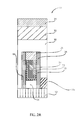
- FIG. 2B depicts a side cross-sectional view in the space between adjacent fin structures (similar to cross-section along section line B-B in FIG. 1 ) at the stage of fabrication of FIG. 2A , in accordance with one embodiment of the present disclosure.
- FIG. 3A depicts a side cross-sectional view through the length of a fin structure of the device (similar to the cross-section along section line A-A in FIG. 1 ) at a stage of fabrication in which the anti-reflection coating and the organic planarization layer are removed and trenches are formed, in accordance with one embodiment of the present disclosure.
- FIG. 3B depicts a side cross-sectional view in the space between adjacent fin structures (similar to cross-section along section line B-B in FIG. 1 ) at the stage of fabrication of FIG. 3A , in accordance with one embodiment of the present disclosure.
- FIG. 4 depicts a side cross-sectional view in the space between adjacent fin structures (similar to cross-section along section line B-B in FIG. 1 ) at the stage of fabrication in which a first spacer material is removed, in accordance with one embodiment of the present disclosure.
- FIG. 5 depicts a side cross-sectional view in the space between adjacent fin structures (similar to cross-section along section line B-B in FIG. 1 ) at a stage of fabrication in which a portion of high-k dielectric material is removed from the metal gate structure in accordance with one embodiment of the present disclosure.
- FIG. 6 depicts a side cross-sectional view through the space between adjacent fin structures (similar to cross-section along section line B-B in FIG. 1 ) at a stage of fabrication following FIG. 5 , in which a second spacer material is formed in accordance with one embodiment of the present disclosure.
- FIG. 7A depicts a side cross-sectional view through the length of a fin structure of the device (similar to the cross-section along section line A-A in FIG. 1 ) at a stage of fabrication in which the second spacer material is subjected to an anisotropic etching procedure to remove portions thereof, in accordance with one embodiment of the present disclosure.
- FIG. 7B depicts a side cross-sectional view in the space between adjacent fin structures (similar to cross-section along section line B-B in FIG. 1 ) at the stage of fabrication of FIG. 7A , in accordance with one embodiment of the present disclosure.
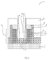
- FIG. 8 depicts a side cross-sectional view through the space between adjacent fin structures (similar to cross-section along section line B-B in FIG. 1 ) at a stage of fabrication in which a metallization layer is formed in the trenches between the second spacer material in accordance with an embodiment of the present disclosure.
- FIG. 9 depicts a side cross-sectional view through the space between adjacent fin structures (similar to cross-section along section line B-B in FIG. 1 ) at a stage of fabrication in which the second spacer material is removed from the trenches in accordance with one embodiment of the present disclosure.
- FIG. 10A depicts a side cross-sectional view through the length of a fin structure of the device (similar to the cross-section along section line A-A in FIG. 1 ) at a stage of fabrication in which a third spacer material is deposited in conformance with the metallization layer and the metal gate structures, forming air gaps and an air gap pinch off region, in accordance with an embodiment of the present principles.
- FIG. 10B depicts a side cross-sectional view in the space between adjacent fin structures (similar to cross-section along section line B-B in FIG. 1 ) at the stage of fabrication of FIG. 7A , in accordance with one embodiment of the present disclosure.
- FIG. 11A depicts a side cross-sectional view through the length of a fin structure of the device (similar to the cross-section along section line A-A in FIG. 1 ) at a stage of fabrication in which chemical mechanical polishing is performed to remove excess third spacer material from the top of the device, in accordance with one embodiment of the present disclosure.
- FIG. 11B depicts a side cross-sectional view in the space between adjacent fin structures (similar to cross-section along section line B-B in FIG. 1 ) at the stage of fabrication of FIG. 11A , in accordance with one embodiment of the present disclosure.
- references in the specification to “one embodiment”, “an embodiment”, “an example embodiment”, etc., indicate that the embodiment described may include a particular feature, structure, or characteristic, but every embodiment may not necessarily include the particular feature, structure, or characteristic. Moreover, such phrases are not necessarily referring to the same embodiment. Further, when a particular feature, structure, or characteristic is described in connection with an embodiment, it is submitted that it is within the knowledge of one skilled in the art to affect such feature, structure, or characteristic in connection with other embodiments whether or not explicitly described.
- the terms “upper”, “lower”, “right”, “left”, “vertical”, “horizontal”, “top”, “bottom”, and derivatives thereof shall relate to the invention, as it is oriented in the drawing figures.
- overlying means that a first element, such as a first structure, is present on a second element, such as a second structure, wherein intervening elements, such as an interface structure, e.g. interface layer, may be present between the first element and the second element.
- intervening elements such as an interface structure, e.g. interface layer
- directly contact means that a first element, such as a first structure, and a second element, such as a second structure, are connected without any intermediary conducting, insulating or semiconductor layers at the interface of the two elements.
- any of the following “/”, “and/or”, and “at least one of”, for example, in the cases of “A/B”, “A and/or B” and “at least one of A and B”, is intended to encompass the selection of the first listed option (A) only, or the selection of the second listed option (B) only, or the selection of both options (A and B).
- such phrasing is intended to encompass the selection of the first listed option (A) only, or the selection of the second listed option (B) only, or the selection of the third listed option (C) only, or the selection of the first and the second listed options (A and B) only, or the selection of the first and third listed options (A and C) only, or the selection of the second and third listed options (B and C) only, or the selection of all three options (A and B and C).
- This may be extended, as readily apparent by one of ordinary skill in this and related arts, for as many items listed.
- a method of forming a semiconductor device is provided with air gap spacers that protects the sensitive high-k dielectric material of the metal gate structures near the metallization layers (which provide a metal contact) over the source and drain regions of the device. In some embodiments, this is done through a sequence of adding and removing sacrificial spacer materials in the locations between the metal layers in the source and drain regions of the device and the body of the gate structure of the device.
- a semiconductor device may be formed including fin structures, source and drain regions, and gate structures.
- the semiconductor device is formed using a replacement metal gate (RMG) structure.
- RMG replacement metal gate
- a replacement metal gate structure is provided by a process sequence, in which a sacrificial gate structure is initially formed on the channel region of the device, and later replaced with a metal gate structure that produces a functional gate structure.
- the functional gate structure functions to switch the semiconductor device from an “on” to “off” state, and vice versa.
- This process sequence may also be referred to as a gate last sequence.
- the gate last process sequence allows for device features, such as, e.g., epitaxial growth of source and drain regions, to be formed while the sacrificial gate structure is in place and before forming the functional gate structure. This provides that the functional gate structure is not subjected to certain process conditions that the sacrificial gate structure is subjected to.
- the functional gate structure (also referred to as replacement metal gate (RMG) structure) may be capped with a silicon nitride material and a first spacer material may be formed around the replacement metal gate structure. As will be described herein, the spacer material (or portions thereof) may be removed at a later time.
- An interlayer dielectric material ILD may then be deposited over the structure, with a silicon anti-reflective coating (SiARC) and an organic planarization layer (OPL) being formed over the ILD layer.
- This arrangement is configured for trench formation, e.g., the trenches are formed in the source and drain regions between the gate structures, and metal materials may be deposited over the source and drain regions. The trenches and the deposited metal materials may provide contacts to the source and drain regions, as well as other active regions of the device.
- the sacrificial spacer material is removed, a portion of the high-k dielectric material of the replacement metal gate structures is removed, a second spacer material is deposited in conformance to the structure, metallization layers are formed over the source/drain regions, the second spacer material is removed, and air gaps are formed between the metallization layers and the replacement metal gate structures that are defined by a third spacer material that forms air gap pinch off region in locations between the metallization layers and the replacement metal gates.
- a semiconductor device is provided having a structure that has little to no parasitic capacitance and in which the high-k dielectric material is not damaged.
- Spacer materials may be formed in the trenches, both before and after metal deposition, the presence of which may shape the metal formation, i.e., metal contacts, and upon removal provide for air gap formation with pinch off regions.
- a spacer material is deposited in the space between the replacement metal gate structures and the metal materials for the contacts that is produced by removing sacrificial spacers, in which the spacer material forms a pinch off seal preventing further spacer material from entering the space.
- the pinch off seal produced by the conformal spacer material leaves an air gap in the space between the replacement metal gates and the metallization formations, e.g., metal contacts, providing air gap insulation in addition to insulation that may be provided by other materials, e.g., low k dielectric spacer material formed in conformance to the walls of the replacement metal gate and metallization formations.
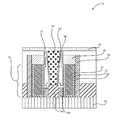
- FIG. 1 depicted is a top plan view showing perspectives views of a one embodiment of a partial semiconductor device 10 , with line A-A showing the perspective of a view through a fin 14 and line B-B showing the perspective of a view through a space 16 present between adjacent fin structures 14 .
- This region of the device may be filled with epitaxial semiconductor material contacting the source and drain regions, e.g., merged source and drain epitaxial semiconductor material.
- Gates 18 positioned within spacers 26 are shown extending perpendicular to the fin structures 14 .
- the view of FIG. 1 is simplified by omitting other parts of the device.
- fin structures 14 are formed on a semiconductor substrate 12 .
- the semiconductor substrate 12 may be made from a semiconductor material, such as, silicon, germanium and silicon-germanium alloy, among other materials and alloys.
- the semiconductor substrate material is silicon.
- the device is provided with a replacement metal gate structure 18 shown passing over the fins 14 .
- a sacrificial gate structure may have been previously formed from polycrystalline silicon, and then replaced with the metal gate structure 18 in a gate last configuration after other aspects of the device are formed, for example, after the source and drain regions 16 are formed by epitaxial growth.
- Replacement metal gate (RMG) structures 18 may include a gate metal material 24 , such as tungsten (W); a work function metal 22 , such as titanium nitride (TiN); and a gate dielectric material 20 , such as a high-k gate dielectric.
- the term “high-k” as used to describe the material of the gate dielectric layer 30 denotes a dielectric material having a dielectric constant greater than silicon oxide (SiO 2 ) at room temperature (20° C. to 25° C.) and atmospheric pressure (1 atm).
- a high-k dielectric material may have a dielectric constant greater than 4.0.
- the high-k gate dielectric material has a dielectric constant greater than 7.0.
- the gate dielectric material 20 is composed of a high-k oxide, such as, for example, HfO 2 , ZrO 2 , Al 2 O 3 , TiO 2 , La 2 O 3 , SrTiO 3 , LaAlO 3 , Y 2 O 3 and mixtures thereof.
- a high-k oxide such as, for example, HfO 2 , ZrO 2 , Al 2 O 3 , TiO 2 , La 2 O 3 , SrTiO 3 , LaAlO 3 , Y 2 O 3 and mixtures thereof.
- high-k dielectric materials for the gate dielectric material 20 include hafnium silicate, hafnium silicon oxynitride or combinations thereof.
- titanium nitride is only one example of a metal containing material that can be used for the work function metal 22 .
- Other examples of work function metals for the replacement metal gate (RMG) gate structures 18 include ruthenium, titanium aluminum, aluminum nitride, and tantalum carbide.
- tungsten (W) is only one example of a composition that can provide the gate metal material 24 .
- the gate metal material 24 may be tantalum (Ta), aluminum (Al), platinum (Pt), gold (Au), silver (Ag), copper (Cu) and alloys thereof.
- the gate dielectric material 20 may surround the work function metal 22 and the gate metal material 24 .
- the gate structure 18 may be capped with a dielectric material 28 , such as silicon nitride, silicon oxide or silicon oxynitride.
- a spacer material 26 surrounds the replacement metal gate (RMG) structure 18 .
- the spacer material 26 may be composed of a dielectric material, such as an oxide, nitride or oxynitride material, that is suitable for sacrifice, e.g., at a later time in the process flow described herein.
- the spacer material 26 may be a silicon oxynitride, e.g., SiNO, or the spacer material may be a silicon boron carbon nitride (SiBCN) material.
- the spacer material 26 may, in such instances, be regarded as a sacrificial gate material.
- An epitaxial growth material 16 a of a semiconductor material, such as crystalline silicon is formed in the source and drain regions of the device.
- the epitaxial growth occurs on both sides of the replacement metal gate structure 18 .
- the epitaxial growth material 16 a may be silicon, germanium, a silicon-germanium (SiGe) alloy and/or carbon doped silicon (Si:C).
- the epitaxial growth material 16 a is SiGe.
- the SiGe layer can be formed, for example, by a selective epitaxial process using a combination of silicon-containing gas, a germanium-containing gas, a carrier gas, and optionally, an etchant gas.
- the silicon containing gas may be a gas such as silane (SiH 4 ), dichlorosilane (SiH 2 Cl 2 ), disilane (Si 2 H 6 ), trisilane (Si 3 H 8 ) or tetrasilane (Si 4 H 10 ).
- the germanium containing gas may be a gas such as germane (GeH 4 ) or digermane (Ge 2 H 6 ).
- the carrier gas may be a gas such as nitrogen, hydrogen, or argon.
- the optional etchant gas may be a gas such as hydrogen chloride (HCl) or chlorine (Cl 2 ).
- the formation may occur at a temperature ranging from about 450° C. to about 900° C.
- the SiGe layer may have a Ge concentration of about 15% to about 100%, preferably from about 20% to about 60%.
- ILD material 30 may be deposited over the substrate 12 , the epitaxial growth material 16 a within the source and drain regions, fin structures 14 , gate structure 18 , spacer 26 and cap 28 .
- ILD material 30 may be selected from silicon containing materials such as SiO 2 , Si 3 N 4 , SiO x N y , SiC, SiCO, SiCOH, and SiCH compounds, with some or all of the Si replaced by Ge, carbon doped oxides, inorganic oxides, inorganic polymers, hybrid polymers, organic polymers such as polyamides or SiLKTM, other carbon containing materials, organo-inorganic materials such as spin-on glasses and silsesquioxane-based materials, and diamond-like carbon (DLC), also known as amorphous hydrogenated carbon ( ⁇ -C:H)). Additional choices for the ILD material include any of the aforementioned materials in porous form, or in a form that changes during processing to or from being porous and/or permeable to being non
- a silicon anti-reflective coating (SiARC) 34 and an organic planarization layer (OPL) 32 are formed over the ILD layer 30 .
- the exemplary anti-reflective coating (SiARC) 34 and an organic planarization layer (OPL) 32 can be replaced or substituted by any other known or unknown pattering methodology used to determine the placement of the source/drain regions in the exemplary dielectric material (ILD) 30 .
- FIGS. 3A and 3B shown is device 10 at a stage of fabrication in which the anti-reflective coating layer 34 and the organic planarization layer 32 are removed, and a trench 38 is formed between replacement metal gates 18 by removing the ILD material 30 and portions of the spacer material 26 from the space between the replacement metal gates 18 .
- the spacer material 26 may also be removed from near the top of the replacement metal gate structures 18 .
- Forming trenches 38 exposes the epitaxial growth material 16 a in the source and drain regions of the device 10 .
- the ILD material 30 may be removed by anisotropic etching, in which the etch rate in the direction normal to the etched surface is greater than in the direction parallel to the etched surface.
- the anisotropic etch may be performed by reactive-ion etching (RIE).
- RIE reactive-ion etching
- Other examples of anisotropic etching that can be used at this point of the proceedings include ion beam etching, plasma etching or laser ablation
- FIGS. 3A and 3B shows misalignment region that may be formed with removal of portions of the spacer 26 and the exposure of the epitaxial growth material 16 a in the source and drain regions. Misalignments become inconsequential with later processing steps described herein.
- the device 10 is shown at a stage of device fabrication in which an isotropic etch is performed to remove a portion of the spacer material 26 to a location that is below the top of the epitaxial growth material 16 a of the source and drain regions, while leaving a portion of spacer materials 26 , i.e., remnant spacer portion, at the bottom of the trench 38 between the epitaxial semiconductor material 16 a of the source and drain regions and the replacement metal gates 18 .
- the removal of spacer material 26 to this extent forms a space 40 between the source/drain regions 16 and the replacement metal gates 18 .
- the etching may be done by RIE, which is selective to the SiNO/SiBCN spacer material 26 .
- the etch may also be conducted by a wet chemical etch or a gas plasma etch and any etch process in which the etching occurs isotropically, e.g., non-directionally, where the etch rate is not substantially greater in any one direction in comparison to all of the etch directions.
- FIG. 5 shown is device 10 at a stage of fabrication in which an isotropic etch is performed to remove the high-k dielectric material 20 from the replacement metal gates 18 that has been exposed in forming the trenches 36 .
- an isotropic etch is performed to remove the high-k dielectric material 20 from the replacement metal gates 18 that has been exposed in forming the trenches 36 .
- the isotropic etch may be a RIE, a wet chemical etch, or a gas plasma etch.
- the size and dimensions of the recess 42 defined by the thickness of the high-k dielectric material 20 and the isotropic etch process that is used.
- the recess 42 may be configured to end above the fin 14 and source/drain region 16 as not to impact device performance though air exposure to active device region high-k dielectric material.
- the second spacer material 44 may be formed by depositing a conformal layer of dielectric material, such as oxides, nitrides or oxynitrides and combinations thereof along the top of the device and in trenches 38 , where the trench sidewalls and trench bottom are covered by the second spacer material 44 .
- the second spacer material 44 is a continuous dielectric material layer on vertical surfaces of the trench sidewall and horizontal surfaces at a base of the trench.
- the epitaxial semiconductor material 16 a that has been formed on the source and drain portions of the fin structures are buried by the deposit of the second spacer material 44 .
- the second spacer material 44 fills the spaces 40 and recesses 42 within the trench 38 .
- the second spacer material 44 may be, but need not be, a dielectric.
- the second spacer material 44 will cleanly decompose within a time and temperature range, and in an atmosphere, which will not adversely affect the function of other structural components.
- an acceptable decomposition temperature would be at or about 350° C.-450° C.
- suitable materials to function as a second spacer material 44 include: polystyrenes; polymethyl methacrylates; polynorbornenes; and polypropylene glycols. Other examples may include oxides and nitrides.
- the second spacer material 44 may be formed by using a blanket layer deposition, such as chemical vapor deposition.
- the second spacer material 44 may have a width ranging from about 2.0 nm to about 15.0 nm.
- FIGS. 7A and 7B depicted is a stage of device fabrication in which the second spacer material 44 is subjected to an anisotropic pull down etch, in which the material of the sacrificial spacer material 44 is removed from the top of the structure and the bottom of the trenches 38 , exposing the epitaxial semiconductor material 16 a of the source and drain regions.
- the anisotropic pull down etch may include anisotropically etching the continuous dielectric material to remove the continuous dielectric material, i.e., sacrificial spacer material 44 , from the horizontal surfaces of the trench and to reduce a width of the continuous dielectric material, i.e., sacrificial spacer material 44 , at an upper surface of the vertical surfaces of the trench to provide a sacrificial spacer 44 (the remaining portion of the sacrificial spacer material may hereafter be referred to as a sacrificial spacer 44 ) having an upper surface with a width W 1 less than a base surface width W 2 of the sacrificial spacer 44 .
- RIE may be used to effect the anisotropic pulldown, in which the etch rate is higher for horizontal surfaces (e.g, those surfaces on the top of the structure and over the source/drain regions) resulting in a tapered profile in the sacrificial spacer 44 that remains at the top of the device 10 .
- the sacrificial spacer 44 remains in conformance with the sides of the trenches and is present along the replacement metal gate and the ILD material 30 .
- the metallization layer provides a metal contact 46 that in electrical communication with the source and drain regions.
- the metal contact 46 may be in direct contact with an epitaxially formed semiconductor material 16 a of at least one of the source region and the drain region.
- the metal contact 46 is situated between the replacement metal gate structures 18 .
- the metal contact 46 may be formed using physical vapor deposition and (PVD) and chemical vapor deposition (CVD).
- Variations of CVD processes suitable for depositing the at least one first gate dielectric layer include, but are not limited to, atmospheric pressure chemical vapor deposition (APCVD), low pressure chemical vapor deposition (LPCVD), plasma enhanced chemical vapor deposition (PECVD), and metal organic chemical vapor deposition (MOCVD).
- APCVD atmospheric pressure chemical vapor deposition
- LPCVD low pressure chemical vapor deposition
- PECVD plasma enhanced chemical vapor deposition
- MOCVD metal organic chemical vapor deposition
- Sputtering is an example of a PVD process.
- the metallization layer may be formed of a metal. Exemplary metals includes titanium (Ti), aluminum (Al), copper (Cu), tungsten (W), platinum (Pt), and gold (Au).
- the metallization layer may also be formed of a doped polysilicon.
- the metallization layer or layers 46 form source/drain contacts that are processed so that the resultant contact surface 47 of the metallization layer 46 upper surface is coplanar with the interlayer dielectric layer 30 and does not cover, e.g., overlap, the sacrificial second spacer 44 .
- the metal contact 46 completely fills the remainder of the opening for the trench 38 .
- the metal contact 46 directly contacts the exposed sidewalls of the second spacers 44 .
- the width W 3 of the upper surface of the metal contact 46 is less than the width W 4 of the base surface of the metal contact 46 , in which the metal contact 46 tapers from the upper width W 3 to the base width W 4 of the metal contact 46 .
- the sacrificial spacer 44 may be removed in a thermal annealing process.
- the sacrificial spacer 44 may be thermally decomposed into a gas, wherein the gas out diffuses through an opening between the metal contact 46 and the gate structure 18 .
- Thermal decomposition of the sacrificial spacer 44 may include annealing the structure depicted in FIG. 8 in a furnace having controlled, inert or vacuum atmosphere. The increase in temperature is slowly ramped to about 350° C. to 450° C. for a time sufficient to complete removal of the sacrificial spacer 44 and its decomposition by-products.
- the end point may be monitored using a mass spectrometer.
- the thermal decomposition method may continue until an entirety of the sacrificial spacer 44 has decomposed, leaving air dielectric, i.e., gaseous air, i.e., no solid material, in its place.
- the second spacer material 44 is removed in a selective etching process. Annealing may be preferred to prevent further modification of recess 42 or modification of remaining high-k dielectric material 20 .
- the dielectric spacer material 50 which may also be referred to as a third spacer material, conforms to the surfaces of the metal contact 46 and the replacement metal gate structures 18 , and forms a layer 50 over the top of the device 10 .
- air gap pinch off regions 52 are formed by the dielectric spacer material 50 .
- the air gap pinch off regions 52 form a seal in the trench 38 between the metallization layer 26 , the nitride cap 28 , and/or the interlayer dielectric material 30 .
- the dielectric spacer material 50 is deposited in conformance with these components. In the narrow spaces at the top of the device, the dielectric spacer material 50 “pinches off” the open space below then pinch off region 52 , forming an air gap 48 between the replacement metal gate 18 and the metallization layer 46 , with the pinch off region 52 of the dielectric spacer material sealing the air gap 48 to the exterior of the device 10 .
- the air gap pinch off spacer material 50 may be applied to the device by chemical vapor deposition (CVD).
- CVD processes suitable for depositing airgap pinch off spacer material 50 include, but are not limited to atmospheric pressure chemical vapor deposition (APCVD), low pressure chemical vapor deposition (LPCVD), plasma enhanced chemical vapor deposition (PECVD), metal organic chemical vapor deposition (MOCVD), atomic layer deposition (ALD), and combinations thereof.
- APCVD atmospheric pressure chemical vapor deposition
- LPCVD low pressure chemical vapor deposition
- PECVD plasma enhanced chemical vapor deposition
- MOCVD metal organic chemical vapor deposition
- ALD atomic layer deposition
- the air gap pinch off spacer material 50 substantially uniformly coats the structure of the device 10 . In the regions where the second spacer material 44 has been removed, pinch-off regions form near the top of the device 10 , leaving an air gap 48 between the walls of the replacement metal gate 18 and the metal contact 46 . Air gap 48 extends in the space between the replacement metal gate 18 and the metal contact 46 .
- the air gap pinch off spacer material 50 is a low-k dielectric material that may contribute to the reduction in parasitic capacitance of the device.
- the low-k dielectric material may have a dielectric constant that is less than about 4.0, e.g., about 3.9.
- the low-k dielectric material has a dielectric constant ranging from about 1.75 to about 3.5.
- the low-k dielectric material has a dielectric constant ranging from about 2.0 to about 3.2.
- the low-k dielectric material has a dielectric constant ranging from about 2.25 to about 3.0.
- low-k dielectric material examples include organosilicate glass (OSG), fluorine doped silicon dioxide, carbon doped silicon dioxide, porous silicon dioxide, porous carbon doped silicon dioxide, spin-on organic polymeric dielectrics (e.g., SILKTM), spin-on silicone based polymeric dielectric (e.g., hydrogen silsesquioxane (HSQ) and methylsilsesquioxane (MSQ), and combinations thereof.
- OSG organosilicate glass
- fluorine doped silicon dioxide carbon doped silicon dioxide
- porous silicon dioxide porous carbon doped silicon dioxide
- spin-on organic polymeric dielectrics e.g., SILKTM
- spin-on silicone based polymeric dielectric e.g., hydrogen silsesquioxane (HSQ) and methylsilsesquioxane (MSQ)
- the air gap pinch off spacer material 50 on the top of the device has been removed, for example, by chemical mechanical polishing (CMP), in one or more polishing steps, employing one or more appropriate slurry compositions.
- CMP may be followed by a wet etch process.
- FIGS. 11A and 11B shows a view of the device 10 in which the air gap pinch off spacer material 50 on the top of the device 10 is removed, for example, by chemical mechanical polishing (CMP), in one or more polishing steps, employing one or more appropriate slurry compositions.
- CMP chemical mechanical polishing
- the recess 42 does not approach the interface region between the fin structure 14 and work function metal 22 that extends over the fin.
- the gate dielectric 20 was not removed in the fabrication of the device, e.g., at the step described above in relation to FIG. 5 , where some gate dielectric material 20 , e.g., high-k dielectric material, was removed from the replacement metal gate structures 18 .
- the gate dielectric material 20 e.g., high-k dielectric material, separates fin structures 14 from the work function metal 22 so as to maintain the device performance and operability.
- the recess 42 does not reach the top of the fin structure 14 and is isolated from the air gap 48 by the air gap spacer pinch off material 50 .
- the air gap spacer material 50 keeps contaminating materials out of the recess 42 and gate dielectric material 20 , e.g., high-k dielectric material.
- the air gaps 48 formed in the pinch off region 52 provide an effective insulating properties that eliminate parasitic capacitance.
- the dielectric constant of air is near unity, as compared to the dielectric constant of SiN, which is about 7-7.5.
- the resulting spacer formed by the air gap 48 affords enhanced electrical performance by reducing parasitic capacitance between the replacement metal gates 18 and the metallization 46 formed over the source/drain regions 16 .
- the structure of the FinFET devices provided with air gaps in pinch off regions formed by dielectric material in accordance with the embodiments of the present principles offer several advantages and improvements. As indicated, parasitic capacitance is reduced, as a result of providing an air gap having a low dielectric constant in place of a traditional spacer, e.g., the spacer 26 that was initially in place around the replacement metal gate structures 18 ;
- Removing a portion of the high-k dielectric material from the sides of the replacement metal gates increases the distance between the metallization layers over the source/drain regions and the gates, which further reduces parasitic capacitance when compared to an air gap of equivalent size to spacer 26 .
- High-k dielectric materials reduce leakage current significantly (e.g., by 100 ⁇ ).
- High-k gate dielectric materials can have a greater thickness than, for example, SiO 2 .
- Use of metal gates with appropriate work functions can provide the proper threshold voltages (V t ) and significantly reduce channel mobility degradation. With the combination of high-k gate dielectrics and metal gates, the transistor performance can be significantly improved, and scaling below ⁇ 50 nm becomes possible; and
- Using the sacrificial spacer material may enable additional control over the metallization layers that are formed, by providing additional space when Hi-K materials are removed from the boundaries of the source/drain contact region.
- the resulting integrated circuit chips can be distributed by the fabricator in raw wafer form (that is, as a single wafer that has multiple unpackaged chips), as a bare die, or in a packaged form.
- the chip is mounted in a single chip package (such as a plastic carrier, with leads that are affixed to a motherboard or other higher level carrier) or in a multichip package (such as a ceramic carrier that has either or both surface interconnections or buried interconnections).
- the chip is then integrated with other chips, discrete circuit elements, and/or other signal processing devices as part of either (a) an intermediate product, such as a motherboard, or (b) an end product.
- the end product can be any product that includes integrated circuit chips, ranging from toys and other low-end applications to advanced computer products having a display, a keyboard or other input device, and a central processor.
Abstract
Description
Claims (20)
Priority Applications (4)
| Application Number | Priority Date | Filing Date | Title |
|---|---|---|---|
| US15/786,828 US10043801B2 (en) | 2016-06-03 | 2017-10-18 | Air gap spacer for metal gates |
| US16/002,590 US10607991B2 (en) | 2016-06-03 | 2018-06-07 | Air gap spacer for metal gates |
| US16/834,548 US11557589B2 (en) | 2016-06-03 | 2020-03-30 | Air gap spacer for metal gates |
| US18/073,294 US20230352480A1 (en) | 2016-06-03 | 2022-12-01 | Air gap spacer for metal gates |
Applications Claiming Priority (3)
| Application Number | Priority Date | Filing Date | Title |
|---|---|---|---|
| US15/173,132 US9608065B1 (en) | 2016-06-03 | 2016-06-03 | Air gap spacer for metal gates |
| US15/371,350 US10553581B2 (en) | 2016-06-03 | 2016-12-07 | Air gap spacer for metal gates |
| US15/786,828 US10043801B2 (en) | 2016-06-03 | 2017-10-18 | Air gap spacer for metal gates |
Related Parent Applications (1)
| Application Number | Title | Priority Date | Filing Date |
|---|---|---|---|
| US15/371,350 Division US10553581B2 (en) | 2016-06-03 | 2016-12-07 | Air gap spacer for metal gates |
Related Child Applications (1)
| Application Number | Title | Priority Date | Filing Date |
|---|---|---|---|
| US16/002,590 Continuation US10607991B2 (en) | 2016-06-03 | 2018-06-07 | Air gap spacer for metal gates |
Publications (2)
| Publication Number | Publication Date |
|---|---|
| US20180158818A1 US20180158818A1 (en) | 2018-06-07 |
| US10043801B2 true US10043801B2 (en) | 2018-08-07 |
Family
ID=58359570
Family Applications (6)
| Application Number | Title | Priority Date | Filing Date |
|---|---|---|---|
| US15/173,132 Active US9608065B1 (en) | 2016-06-03 | 2016-06-03 | Air gap spacer for metal gates |
| US15/371,350 Active US10553581B2 (en) | 2016-06-03 | 2016-12-07 | Air gap spacer for metal gates |
| US15/786,828 Active US10043801B2 (en) | 2016-06-03 | 2017-10-18 | Air gap spacer for metal gates |
| US16/002,590 Active US10607991B2 (en) | 2016-06-03 | 2018-06-07 | Air gap spacer for metal gates |
| US16/834,548 Active 2036-11-07 US11557589B2 (en) | 2016-06-03 | 2020-03-30 | Air gap spacer for metal gates |
| US18/073,294 Pending US20230352480A1 (en) | 2016-06-03 | 2022-12-01 | Air gap spacer for metal gates |
Family Applications Before (2)
| Application Number | Title | Priority Date | Filing Date |
|---|---|---|---|
| US15/173,132 Active US9608065B1 (en) | 2016-06-03 | 2016-06-03 | Air gap spacer for metal gates |
| US15/371,350 Active US10553581B2 (en) | 2016-06-03 | 2016-12-07 | Air gap spacer for metal gates |
Family Applications After (3)
| Application Number | Title | Priority Date | Filing Date |
|---|---|---|---|
| US16/002,590 Active US10607991B2 (en) | 2016-06-03 | 2018-06-07 | Air gap spacer for metal gates |
| US16/834,548 Active 2036-11-07 US11557589B2 (en) | 2016-06-03 | 2020-03-30 | Air gap spacer for metal gates |
| US18/073,294 Pending US20230352480A1 (en) | 2016-06-03 | 2022-12-01 | Air gap spacer for metal gates |
Country Status (1)
| Country | Link |
|---|---|
| US (6) | US9608065B1 (en) |
Cited By (2)
| Publication number | Priority date | Publication date | Assignee | Title |
|---|---|---|---|---|
| US20180294263A1 (en) * | 2016-06-03 | 2018-10-11 | International Business Machines Corporation | Air gap spacer for metal gates |
| US10388770B1 (en) * | 2018-03-19 | 2019-08-20 | Globalfoundries Inc. | Gate and source/drain contact structures positioned above an active region of a transistor device |
Families Citing this family (65)
| Publication number | Priority date | Publication date | Assignee | Title |
|---|---|---|---|---|
| US9601567B1 (en) * | 2015-10-30 | 2017-03-21 | Taiwan Semiconductor Manufacturing Co., Ltd. | Multiple Fin FET structures having an insulating separation plug |
| US9842931B1 (en) | 2016-06-09 | 2017-12-12 | International Business Machines Corporation | Self-aligned shallow trench isolation and doping for vertical fin transistors |
| US9911804B1 (en) * | 2016-08-22 | 2018-03-06 | International Business Machines Corporation | Vertical fin field effect transistor with air gap spacers |
| US10727297B2 (en) * | 2016-09-12 | 2020-07-28 | Samsung Electronics Co., Ltd. | Complimentary metal-oxide-semiconductor circuit having transistors with different threshold voltages and method of manufacturing the same |
| US9917196B1 (en) * | 2016-10-14 | 2018-03-13 | International Business Machines Corporation | Semiconductor device and method of forming the semiconductor device |
| US10177241B2 (en) * | 2016-10-28 | 2019-01-08 | Globalfoundries Inc. | Methods of forming a gate contact for a transistor above the active region and an air gap adjacent the gate of the transistor |
| US9806078B1 (en) * | 2016-11-02 | 2017-10-31 | Globalfoundries Inc. | FinFET spacer formation on gate sidewalls, between the channel and source/drain regions |
| US10164104B2 (en) * | 2016-11-04 | 2018-12-25 | Globalfoundries Inc. | Method to form air-gap spacers and air-gap spacer-containing structures |
| BR112019008514A2 (en) * | 2016-12-02 | 2019-07-09 | Intel Corp | semiconductor device having voltage inducing elements at the fin end |
| US10319627B2 (en) * | 2016-12-13 | 2019-06-11 | Globalfoundries Inc. | Air-gap spacers for field-effect transistors |
| US10522642B2 (en) * | 2016-12-14 | 2019-12-31 | Taiwan Semiconductor Manufacturing Co. Ltd. | Semiconductor device with air-spacer |
| DE102017113681A1 (en) | 2016-12-14 | 2018-06-14 | Taiwan Semiconductor Manufacturing Co. Ltd. | SEMICONDUCTOR CONSTRUCTION ELEMENT WITH AIR SPACER HOLDER |
| US10079290B2 (en) | 2016-12-30 | 2018-09-18 | United Microelectronics Corp. | Semiconductor device having asymmetric spacer structures |
| US10026824B1 (en) * | 2017-01-18 | 2018-07-17 | Globalfoundries Inc. | Air-gap gate sidewall spacer and method |
| CN108573926B (en) * | 2017-03-09 | 2020-01-21 | 联华电子股份有限公司 | Semiconductor memory device and method of manufacturing the same |
| US10566245B2 (en) * | 2017-04-26 | 2020-02-18 | Samsung Electronics Co., Ltd. | Method of fabricating gate all around semiconductor device |
| US10269983B2 (en) * | 2017-05-09 | 2019-04-23 | Globalfoundries Inc. | Stacked nanosheet field-effect transistor with air gap spacers |
| US10522392B2 (en) * | 2017-05-31 | 2019-12-31 | Taiwan Semiconductor Manufacturing Co., Ltd. | Semiconductor device and method of fabricating the same |
| CN109216357B (en) | 2017-06-30 | 2021-04-20 | 联华电子股份有限公司 | Semiconductor structure and manufacturing method thereof |
| CN109216451A (en) * | 2017-07-03 | 2019-01-15 | 中芯国际集成电路制造(上海)有限公司 | Semiconductor structure and forming method thereof |
| KR102365108B1 (en) | 2017-08-01 | 2022-02-18 | 삼성전자주식회사 | Integrated Circuit devices |
| CN109904120B (en) | 2017-12-11 | 2021-12-14 | 中芯国际集成电路制造(北京)有限公司 | Semiconductor device and method for manufacturing the same |
| US10411114B2 (en) * | 2017-12-21 | 2019-09-10 | International Business Machines Corporation | Air gap spacer with wrap-around etch stop layer under gate spacer |
| US10211092B1 (en) * | 2018-01-28 | 2019-02-19 | International Business Machines Corporation | Transistor with robust air spacer |
| TWI705529B (en) * | 2018-02-15 | 2020-09-21 | 美商應用材料股份有限公司 | Airgap formation processes |
| US10573552B2 (en) * | 2018-03-15 | 2020-02-25 | Samsung Electronics Co., Ltd. | Semiconductor device and method of fabricating the same |
| US11011617B2 (en) | 2018-03-23 | 2021-05-18 | International Business Machines Corporation | Formation of a partial air-gap spacer |
| US10573724B2 (en) * | 2018-04-10 | 2020-02-25 | International Business Machines Corporation | Contact over active gate employing a stacked spacer |
| CN110400751A (en) * | 2018-04-25 | 2019-11-01 | 中芯国际集成电路制造(上海)有限公司 | A kind of semiconductor devices and its manufacturing method and electronic device |
| US11139385B2 (en) * | 2018-05-17 | 2021-10-05 | International Business Machines Corporation | Interface-less contacts to source/drain regions and gate electrode over active portion of device |
| US10608096B2 (en) * | 2018-06-11 | 2020-03-31 | International Business Machines Corporation | Formation of air gap spacers for reducing parasitic capacitance |
| US10854503B2 (en) * | 2018-07-16 | 2020-12-01 | Taiwan Semiconductor Manufacturing Co., Ltd. | Semiconductor structure with air gap and method sealing the air gap |
| US10700180B2 (en) | 2018-07-27 | 2020-06-30 | Taiwan Semiconductor Manufacturing Co., Ltd. | Semiconductor structure and manufacturing method thereof |
| CN110858578B (en) * | 2018-08-23 | 2021-07-13 | 联华电子股份有限公司 | Die seal ring and manufacturing method thereof |
| US10580692B1 (en) * | 2018-09-12 | 2020-03-03 | International Business Machines Corporation | Integration of air spacer with self-aligned contact in transistor |
| US10923565B2 (en) * | 2018-09-27 | 2021-02-16 | Taiwan Semiconductor Manufacturing Co., Ltd. | Self-aligned contact air gap formation |
| US10825721B2 (en) * | 2018-10-23 | 2020-11-03 | Taiwan Semiconductor Manufacturing Co., Ltd. | Insulating cap on contact structure and method for forming the same |
| US10971408B2 (en) * | 2018-10-31 | 2021-04-06 | Taiwan Semiconductor Manufacturing Co., Ltd. | Contact air gap formation and structures thereof |
| US11172156B2 (en) * | 2018-11-30 | 2021-11-09 | Taiwan Semiconductor Manufacturing Company Limited | Semiconductor device and method of manufacture |
| DE102019118390A1 (en) | 2018-11-30 | 2020-06-04 | Taiwan Semiconductor Manufacturing Co. Ltd. | Semiconductor device and manufacturing method |
| US10629694B1 (en) * | 2018-11-30 | 2020-04-21 | Globalfoundries Inc. | Gate contact and cross-coupling contact formation |
| US10559655B1 (en) | 2018-12-05 | 2020-02-11 | United Microelectronics Corp. | Semiconductor device and method for manufacturing the same |
| US11164866B2 (en) * | 2019-02-20 | 2021-11-02 | Taiwan Semiconductor Manufacturing Co., Ltd. | Semiconductor structure and method for manufacturing the same |
| US10872810B2 (en) * | 2019-03-14 | 2020-12-22 | Taiwan Semiconductor Manufacturing Co., Ltd. | Fin field effect transistor device structure and method for forming the same |
| CN111696867B (en) * | 2019-03-15 | 2023-09-19 | 中芯国际集成电路制造(上海)有限公司 | Semiconductor structure and forming method |
| US11482456B2 (en) * | 2019-03-21 | 2022-10-25 | Globalfoundries U.S. Inc. | Forming two portion spacer after metal gate and contact formation, and related IC structure |
| US10903331B2 (en) | 2019-03-25 | 2021-01-26 | International Business Machines Corporation | Positioning air-gap spacers in a transistor for improved control of parasitic capacitance |
| CN111863963A (en) * | 2019-04-24 | 2020-10-30 | 中芯国际集成电路制造(上海)有限公司 | Semiconductor device and method of forming the same |
| US10832962B1 (en) * | 2019-05-22 | 2020-11-10 | International Business Machines Corporation | Formation of an air gap spacer using sacrificial spacer layer |
| US11152486B2 (en) * | 2019-07-15 | 2021-10-19 | Taiwan Semiconductor Manufacturing Co., Ltd. | FinFET semiconductor device having source/drain contact(s) separated by airgap spacer(s) from the gate stack(s) to reduce parasitic capacitance |
| US11587870B2 (en) | 2019-08-13 | 2023-02-21 | Micron Technology, Inc. | Apparatus comprising aluminum interconnections, memory devices comprising interconnections, and related methods |
| US11189531B2 (en) | 2019-08-23 | 2021-11-30 | Taiwan Semiconductor Manufacturing Company, Ltd. | Fin field-effect transistor device and method |
| US11282920B2 (en) | 2019-09-16 | 2022-03-22 | Taiwan Semiconductor Manufacturing Co., Ltd. | Semiconductor device with air gap on gate structure and method for forming the same |
| DE102019133935B4 (en) * | 2019-09-30 | 2022-11-03 | Taiwan Semiconductor Manufacturing Co. Ltd. | METHOD OF FORMING TRANSISTOR SPACER STRUCTURES |
| KR20210038762A (en) * | 2019-09-30 | 2021-04-08 | 삼성전자주식회사 | Semiconductor devices |
| US11094796B2 (en) | 2019-09-30 | 2021-08-17 | Taiwan Semiconductor Manufacturing Co., Ltd. | Transistor spacer structures |
| CN113013226B (en) * | 2019-12-20 | 2024-02-06 | 台湾积体电路制造股份有限公司 | Semiconductor device and method of forming semiconductor device |
| US11502166B2 (en) * | 2019-12-20 | 2022-11-15 | Taiwan Semiconductor Manufacturing Co., Ltd. | Seal material for air gaps in semiconductor devices |
| US11296187B2 (en) * | 2019-12-20 | 2022-04-05 | Taiwan Semiconductor Manufacturing Co., Ltd. | Seal material for air gaps in semiconductor devices |
| US11264419B2 (en) * | 2019-12-30 | 2022-03-01 | Omnivision Technologies, Inc. | Image sensor with fully depleted silicon on insulator substrate |
| US11417750B2 (en) | 2020-01-31 | 2022-08-16 | Taiwan Semiconductor Manufacturing Co., Ltd. | Gate air spacer for fin-like field effect transistor |
| US11489053B2 (en) | 2020-04-09 | 2022-11-01 | Taiwan Semiconductor Manufacturing Co., Ltd. | Semiconductor device and method |
| US20220037496A1 (en) * | 2020-07-31 | 2022-02-03 | Taiwan Semiconductor Manufacturing Co., Ltd. | Multigate device with air gap spacer and backside rail contact and method of fabricating thereof |
| CN115989577A (en) * | 2020-09-25 | 2023-04-18 | 中芯国际集成电路制造(上海)有限公司 | Semiconductor structure and forming method thereof |
| US11876114B2 (en) * | 2021-09-07 | 2024-01-16 | International Business Machines Corporation | Airgap gate spacer |
Citations (10)
| Publication number | Priority date | Publication date | Assignee | Title |
|---|---|---|---|---|
| US7622761B2 (en) | 2006-03-17 | 2009-11-24 | Samsung Electronics Co., Ltd. | Non-volatile memory device and method of manufacturing the same |
| US20130092984A1 (en) | 2011-10-13 | 2013-04-18 | Taiwan Semiconductor Manufacturing Company, Ltd. | Finfet device and method of manufacturing same |
| US20130224141A1 (en) | 2010-09-24 | 2013-08-29 | Scott Robson | Method for straightening hair |
| US8637930B2 (en) * | 2011-10-13 | 2014-01-28 | International Business Machines Company | FinFET parasitic capacitance reduction using air gap |
| US8841711B1 (en) | 2013-03-12 | 2014-09-23 | Globalfoundries Inc. | Methods of increasing space for contact elements by using a sacrificial liner and the resulting device |
| US8916936B2 (en) | 2012-08-22 | 2014-12-23 | Samsung Electronics Co., Ltd. | Transistor structure of a semiconductor device |
| US20150021683A1 (en) | 2013-07-22 | 2015-01-22 | Globalfoundries Inc. | Methods of forming semiconductor device with self-aligned contact elements and the resulting devices |
| US20150025557A1 (en) | 2012-02-16 | 2015-01-22 | E-Med Co., Ltd. | Tool for surgical operation using ultrasonic waves |
| US20150243760A1 (en) | 2014-02-27 | 2015-08-27 | International Business Machines Corporation | Low-k spacer for rmg finfet formation |
| US9123774B2 (en) | 2013-01-23 | 2015-09-01 | Samsung Electronics Co., Ltd. | Semiconductor devices and methods of fabricating the same |
Family Cites Families (14)
| Publication number | Priority date | Publication date | Assignee | Title |
|---|---|---|---|---|
| US20080217775A1 (en) * | 2007-03-07 | 2008-09-11 | Taiwan Semiconductor Manufacturing Co., Ltd. | Method of forming contact plugs for eliminating tungsten seam issue |
| JP5059204B2 (en) * | 2011-02-21 | 2012-10-24 | 株式会社東芝 | Manufacturing method of semiconductor memory device |
| US20130221414A1 (en) | 2012-02-27 | 2013-08-29 | Chao Zhao | Semiconductor FET and Method for Manufacturing the Same |
| US10535735B2 (en) * | 2012-06-29 | 2020-01-14 | Intel Corporation | Contact resistance reduced P-MOS transistors employing Ge-rich contact layer |
| CN103855093B (en) | 2012-11-30 | 2016-07-06 | 中国科学院微电子研究所 | Semiconductor device and manufacture method thereof |
| KR102046976B1 (en) * | 2012-12-04 | 2019-12-02 | 삼성전자주식회사 | Semiconductor memory device and method for fabricating the same |
| US9871121B2 (en) | 2014-03-10 | 2018-01-16 | Qualcomm Incorporated | Semiconductor device having a gap defined therein |
| US9484250B2 (en) | 2015-03-10 | 2016-11-01 | International Business Machines Corporation | Air gap contact formation for reducing parasitic capacitance |
| US10062763B2 (en) * | 2015-05-27 | 2018-08-28 | Qualcomm Incorporated | Method and apparatus for selectively forming nitride caps on metal gate |
| US20170103981A1 (en) * | 2015-10-12 | 2017-04-13 | United Microelectronics Corp. | Method for fabricating contacts to non-planar mos transistors in semiconductor device |
| US9536982B1 (en) * | 2015-11-03 | 2017-01-03 | International Business Machines Corporation | Etch stop for airgap protection |
| DE112016006691T5 (en) * | 2016-04-01 | 2018-12-06 | Intel Corporation | Transistor Gate Trenching processing to reduce capacitance and resistance |
| US9608065B1 (en) * | 2016-06-03 | 2017-03-28 | International Business Machines Corporation | Air gap spacer for metal gates |
| US9892961B1 (en) | 2016-08-09 | 2018-02-13 | International Business Machines Corporation | Air gap spacer formation for nano-scale semiconductor devices |
-
2016
- 2016-06-03 US US15/173,132 patent/US9608065B1/en active Active
- 2016-12-07 US US15/371,350 patent/US10553581B2/en active Active
-
2017
- 2017-10-18 US US15/786,828 patent/US10043801B2/en active Active
-
2018
- 2018-06-07 US US16/002,590 patent/US10607991B2/en active Active
-
2020
- 2020-03-30 US US16/834,548 patent/US11557589B2/en active Active
-
2022
- 2022-12-01 US US18/073,294 patent/US20230352480A1/en active Pending
Patent Citations (11)
| Publication number | Priority date | Publication date | Assignee | Title |
|---|---|---|---|---|
| US7622761B2 (en) | 2006-03-17 | 2009-11-24 | Samsung Electronics Co., Ltd. | Non-volatile memory device and method of manufacturing the same |
| US20130224141A1 (en) | 2010-09-24 | 2013-08-29 | Scott Robson | Method for straightening hair |
| US20130092984A1 (en) | 2011-10-13 | 2013-04-18 | Taiwan Semiconductor Manufacturing Company, Ltd. | Finfet device and method of manufacturing same |
| US8637930B2 (en) * | 2011-10-13 | 2014-01-28 | International Business Machines Company | FinFET parasitic capacitance reduction using air gap |
| US8637384B2 (en) | 2011-10-13 | 2014-01-28 | International Business Machines Corporation | FinFET parasitic capacitance reduction using air gap |
| US20150025557A1 (en) | 2012-02-16 | 2015-01-22 | E-Med Co., Ltd. | Tool for surgical operation using ultrasonic waves |
| US8916936B2 (en) | 2012-08-22 | 2014-12-23 | Samsung Electronics Co., Ltd. | Transistor structure of a semiconductor device |
| US9123774B2 (en) | 2013-01-23 | 2015-09-01 | Samsung Electronics Co., Ltd. | Semiconductor devices and methods of fabricating the same |
| US8841711B1 (en) | 2013-03-12 | 2014-09-23 | Globalfoundries Inc. | Methods of increasing space for contact elements by using a sacrificial liner and the resulting device |
| US20150021683A1 (en) | 2013-07-22 | 2015-01-22 | Globalfoundries Inc. | Methods of forming semiconductor device with self-aligned contact elements and the resulting devices |
| US20150243760A1 (en) | 2014-02-27 | 2015-08-27 | International Business Machines Corporation | Low-k spacer for rmg finfet formation |
Non-Patent Citations (1)
| Title |
|---|
| List of IBM Patents or Patent Applications Treated as Related dated Oct. 18, 2017, 2 pages. |
Cited By (4)
| Publication number | Priority date | Publication date | Assignee | Title |
|---|---|---|---|---|
| US20180294263A1 (en) * | 2016-06-03 | 2018-10-11 | International Business Machines Corporation | Air gap spacer for metal gates |
| US10607991B2 (en) * | 2016-06-03 | 2020-03-31 | Tessera, Inc. | Air gap spacer for metal gates |
| US11557589B2 (en) | 2016-06-03 | 2023-01-17 | Tessera, LLC | Air gap spacer for metal gates |
| US10388770B1 (en) * | 2018-03-19 | 2019-08-20 | Globalfoundries Inc. | Gate and source/drain contact structures positioned above an active region of a transistor device |
Also Published As
| Publication number | Publication date |
|---|---|
| US20180294263A1 (en) | 2018-10-11 |
| US20200235094A1 (en) | 2020-07-23 |
| US20180158818A1 (en) | 2018-06-07 |
| US20230352480A1 (en) | 2023-11-02 |
| US20170352657A1 (en) | 2017-12-07 |
| US11557589B2 (en) | 2023-01-17 |
| US9608065B1 (en) | 2017-03-28 |
| US10607991B2 (en) | 2020-03-31 |
| US10553581B2 (en) | 2020-02-04 |
Similar Documents
| Publication | Publication Date | Title |
|---|---|---|
| US11557589B2 (en) | Air gap spacer for metal gates | |
| US10177237B2 (en) | Etch stop for airgap protection | |
| US11251285B2 (en) | Approach to control over-etching of bottom spacers in vertical fin field effect transistor devices | |
| US8765556B2 (en) | Method of fabricating strained structure in semiconductor device | |
| US10115724B1 (en) | Double diffusion break gate structure without vestigial antenna capacitance | |
| US11233140B2 (en) | Semiconductor device and manufacturing method thereof | |
| US20240105719A1 (en) | Integrated circuits with finfet gate structures | |
| US11784233B2 (en) | Integrated circuit structure with backside via rail | |
| TWI754266B (en) | Semiconductor device and manufacturing method thereof | |
| KR20200124618A (en) | Semiconductor device and manufacturing method thereof | |
| TW202027170A (en) | Method of manufacturing a semiconductor device and a semiconductor device | |
| KR102447651B1 (en) | Transistor gate structure and method of forming | |
| KR102549862B1 (en) | Nano-fet semiconductor device and method of forming | |
| US11640941B2 (en) | Semiconductor devices including metal gate protection and methods of fabrication thereof | |
| TW202139366A (en) | Semiconductor devices and methods for manufacturing the same | |
| US11961911B2 (en) | Semiconductor devices including channel regions having non-uniform Ge concentration | |
| KR102571375B1 (en) | Method of manufacturing a semiconductor device and a semiconductor device | |
| US20230402512A1 (en) | Semiconductor device with dielectric liners on gate refill metal | |
| TW202322399A (en) | Semiconductor device and method of manufacturing the same | |
| KR20200124625A (en) | Semiconductor device and manufacturing method thereof |
Legal Events
| Date | Code | Title | Description |
|---|---|---|---|
| AS | Assignment |
Owner name: INTERNATIONAL BUSINESS MACHINES CORPORATION, NEW Y Free format text: ASSIGNMENT OF ASSIGNORS INTEREST;ASSIGNORS:BERGENDAHL, MARC A.;CHENG, KANGGUO;LIE, FEE LI;AND OTHERS;SIGNING DATES FROM 20160601 TO 20160603;REEL/FRAME:043891/0821 |
|
| FEPP | Fee payment procedure |
Free format text: ENTITY STATUS SET TO UNDISCOUNTED (ORIGINAL EVENT CODE: BIG.); ENTITY STATUS OF PATENT OWNER: LARGE ENTITY |
|
| STCF | Information on status: patent grant |
Free format text: PATENTED CASE |
|
| AS | Assignment |
Owner name: TESSERA, INC., CALIFORNIA Free format text: ASSIGNMENT OF ASSIGNORS INTEREST;ASSIGNOR:INTERNATIONAL BUSINESS MACHINES CORPORATION;REEL/FRAME:051489/0557 Effective date: 20191227 |
|
| AS | Assignment |
Owner name: BANK OF AMERICA, N.A., NORTH CAROLINA Free format text: SECURITY INTEREST;ASSIGNORS:ROVI SOLUTIONS CORPORATION;ROVI TECHNOLOGIES CORPORATION;ROVI GUIDES, INC.;AND OTHERS;REEL/FRAME:053468/0001 Effective date: 20200601 |
|
| MAFP | Maintenance fee payment |
Free format text: PAYMENT OF MAINTENANCE FEE, 4TH YEAR, LARGE ENTITY (ORIGINAL EVENT CODE: M1551); ENTITY STATUS OF PATENT OWNER: LARGE ENTITY Year of fee payment: 4 |
|
| AS | Assignment |
Owner name: TESSERA LLC, CALIFORNIA Free format text: CHANGE OF NAME;ASSIGNOR:TESSERA, INC.;REEL/FRAME:059498/0010 Effective date: 20211001 |