US10042258B2 - Composition for forming a resist upper-layer film and method for producing a semiconductor device using the composition - Google Patents
Composition for forming a resist upper-layer film and method for producing a semiconductor device using the composition Download PDFInfo
- Publication number
- US10042258B2 US10042258B2 US15/324,542 US201515324542A US10042258B2 US 10042258 B2 US10042258 B2 US 10042258B2 US 201515324542 A US201515324542 A US 201515324542A US 10042258 B2 US10042258 B2 US 10042258B2
- Authority
- US
- United States
- Prior art keywords
- group
- polymer
- resist
- composition
- carbon atoms
- Prior art date
- Legal status (The legal status is an assumption and is not a legal conclusion. Google has not performed a legal analysis and makes no representation as to the accuracy of the status listed.)
- Active
Links
- 0 CC.CC.CC.CC.CC.CC.CC.CC.CC.CC.CC.CC.CC.CC.CC.CC.CC.CC.CC.CC.CC.CC.CC.CC.CC.CC.CC.CC.cc.cc Chemical compound CC.CC.CC.CC.CC.CC.CC.CC.CC.CC.CC.CC.CC.CC.CC.CC.CC.CC.CC.CC.CC.CC.CC.CC.CC.CC.CC.CC.cc.cc 0.000 description 12
- CRSOQBOWXPBRES-UHFFFAOYSA-N CC(C)(C)C Chemical compound CC(C)(C)C CRSOQBOWXPBRES-UHFFFAOYSA-N 0.000 description 3
- BXDRGXSUOZOUGL-UHFFFAOYSA-N C1=CC2=C(C=C1)C1=C/C=C/C=C\1C2.C1=CC2=CC=CC(CC3=CC=CC4=C3C=CC=C4)=C2C=C1.C1=CC=C(C(CC(C2=CC=CC=C2)C2=CC=CC=C2)C2=CC=CC=C2)C=C1.C1=CC=C2C=CC=CC2=C1.C1=CC=C2C=CC=CC2=C1.CC.CC.CC.CC.CC.CC.CC.CC.CC.CC.CC.CC.CC.CC.CC.CC.CC.CC.CC.CC.CC.CC.CC.CC.CC.CC.CC(C)C.CC(C1=CC=CC=C1)(C1=CC=CC=C1)C1=CC=CC=C1 Chemical compound C1=CC2=C(C=C1)C1=C/C=C/C=C\1C2.C1=CC2=CC=CC(CC3=CC=CC4=C3C=CC=C4)=C2C=C1.C1=CC=C(C(CC(C2=CC=CC=C2)C2=CC=CC=C2)C2=CC=CC=C2)C=C1.C1=CC=C2C=CC=CC2=C1.C1=CC=C2C=CC=CC2=C1.CC.CC.CC.CC.CC.CC.CC.CC.CC.CC.CC.CC.CC.CC.CC.CC.CC.CC.CC.CC.CC.CC.CC.CC.CC.CC.CC(C)C.CC(C1=CC=CC=C1)(C1=CC=CC=C1)C1=CC=CC=C1 BXDRGXSUOZOUGL-UHFFFAOYSA-N 0.000 description 2
- VITJQZXMCCHHKO-UHFFFAOYSA-N C1=CC=C2C=CC=CC2=C1.CC.CC.CCC.CCC Chemical compound C1=CC=C2C=CC=CC2=C1.CC.CC.CCC.CCC VITJQZXMCCHHKO-UHFFFAOYSA-N 0.000 description 2
- PLIAIWZTHLRCEG-UHFFFAOYSA-N CC.CC(C)C1=C2OCOC2=CC=C1.CC(C)C1=CC(O)=C(O)C=C1.CC1=CC(C(C)C)=CC(C(F)(F)F)=C1.OC1=CC=CC2=C(O)C=CC=C12.OC1=CC=CC2=C(O)C=CC=C12.OC1=CC=CC2=C(O)C=CC=C12 Chemical compound CC.CC(C)C1=C2OCOC2=CC=C1.CC(C)C1=CC(O)=C(O)C=C1.CC1=CC(C(C)C)=CC(C(F)(F)F)=C1.OC1=CC=CC2=C(O)C=CC=C12.OC1=CC=CC2=C(O)C=CC=C12.OC1=CC=CC2=C(O)C=CC=C12 PLIAIWZTHLRCEG-UHFFFAOYSA-N 0.000 description 2
- XBNTXINRZTXLHG-UHFFFAOYSA-N CCC(C)(C)C(=O)O.CCC(CC(CC(CC(CC(CC(CC(CC(CC(CC(CC(CC(CC(CC(CC(CC(CC(CC(CC(CC(CC(CC(CC(CC(CC(CC(CC(CC(CC(CC(CC(CC(CC(CC(CC(CC(CC(CC(CC(CC(CC(CC(CC(CC(CC(CC(CC(CC(CC(CC(CC(CC(CC(CC(CC(CC(CC(CC(CC(CC(C)C1=CC=C(C(C)(C)C)C=C1)C1=CC=C(C(C)(C)C)C=C1)C1=CC=C(C(C)(C)C)C=C1)C1=CC=C(C(C)(C)C)C=C1)C1=CC=C(C(C)(C)C)C=C1)C1=CC=C(C(C)(C)C)C=C1)C1=CC=C(C(C)(C)C)C=C1)C1=CC=C(C(C)(C)C)C=C1)C1=CC=C(C(C)(C)C)C=C1)C1=CC=C(C(C)(C)C)C=C1)C1=CC=C(C(C)(C)C)C=C1)C1=CC=C(C(C)(C)C)C=C1)C1=CC=C(C(C)(C)C)C=C1)C1=CC=C(C(C)(C)C)C=C1)C1=CC=C(C(C)(C)C)C=C1)C1=CC=C(C(C)(C)C)C=C1)C1=CC=C(C(C)(C)C)C=C1)C1=CC=C(C(C)(C)C)C=C1)C1=CC=C(C(C)(C)C)C=C1)C1=CC=C(C(C)(C)C)C=C1)C1=CC=C(C(C)(C)C)C=C1)C1=CC=C(C(C)(C)C)C=C1)C1=CC=C(C(C)(C)C)C=C1)C1=CC=C(C(C)(C)C)C=C1)C1=CC=C(C(C)(C)C)C=C1)C1=CC=C(C(C)(C)C)C=C1)C1=CC=C(C(C)(C)C)C=C1)C1=CC=C(C(C)(C)C)C=C1)C1=CC=C(C(C)(C)C)C=C1)C1=CC=C(C(C)(C)C)C=C1)C1=CC=C(C(C)(C)C)C=C1)C1=CC=C(C(C)(C)C)C=C1)C1=CC=C(C(C)(C)C)C=C1)C1=CC=C(C(C)(C)C)C=C1)C1=CC=C(C(C)(C)C)C=C1)C1=CC=C(C(C)(C)C)C=C1)C1=CC=C(C(C)(C)C)C=C1)C1=CC=C(C(C)(C)C)C=C1)C1=CC=C(C(C)(C)C)C=C1)C1=CC=C(C(C)(C)C)C=C1)C1=CC=C(C(C)(C)C)C=C1)C1=CC=C(C(C)(C)C)C=C1)C1=CC=C(C(C)(C)C)C=C1)C1=CC=C(C(C)(C)C)C=C1)C1=CC=C(C(C)(C)C)C=C1)C1=CC=C(C(C)(C)C)C=C1)C1=CC=C(C(C)(C)C)C=C1)C1=CC=C(C(C)(C)C)C=C1)C1=CC=C(C(C)(C)C)C=C1)C1=CC=C(C(C)(C)C)C=C1)C1=CC=C(C(C)(C)C)C=C1)C1=CC=C(C(C)(C)C)C=C1)C1=CC=C(C(C)(C)C)C=C1)C1=CC=C(C(C)(C)C)C=C1)C1=CC=C(C(C)(C)C)C=C1)C1=CC=C(C(C)(C)C)C=C1)C1=CC=C(C(C)(C)C)C=C1)C1=CC=C(C(C)(C)C)C=C1)C1=CC=C(C(C)(C)C)C=C1)C1=CC=C(C(C)(C)C)C=C1 Chemical compound CCC(C)(C)C(=O)O.CCC(CC(CC(CC(CC(CC(CC(CC(CC(CC(CC(CC(CC(CC(CC(CC(CC(CC(CC(CC(CC(CC(CC(CC(CC(CC(CC(CC(CC(CC(CC(CC(CC(CC(CC(CC(CC(CC(CC(CC(CC(CC(CC(CC(CC(CC(CC(CC(CC(CC(CC(CC(CC(CC(CC(CC(CC(CC(CC(CC(C)C1=CC=C(C(C)(C)C)C=C1)C1=CC=C(C(C)(C)C)C=C1)C1=CC=C(C(C)(C)C)C=C1)C1=CC=C(C(C)(C)C)C=C1)C1=CC=C(C(C)(C)C)C=C1)C1=CC=C(C(C)(C)C)C=C1)C1=CC=C(C(C)(C)C)C=C1)C1=CC=C(C(C)(C)C)C=C1)C1=CC=C(C(C)(C)C)C=C1)C1=CC=C(C(C)(C)C)C=C1)C1=CC=C(C(C)(C)C)C=C1)C1=CC=C(C(C)(C)C)C=C1)C1=CC=C(C(C)(C)C)C=C1)C1=CC=C(C(C)(C)C)C=C1)C1=CC=C(C(C)(C)C)C=C1)C1=CC=C(C(C)(C)C)C=C1)C1=CC=C(C(C)(C)C)C=C1)C1=CC=C(C(C)(C)C)C=C1)C1=CC=C(C(C)(C)C)C=C1)C1=CC=C(C(C)(C)C)C=C1)C1=CC=C(C(C)(C)C)C=C1)C1=CC=C(C(C)(C)C)C=C1)C1=CC=C(C(C)(C)C)C=C1)C1=CC=C(C(C)(C)C)C=C1)C1=CC=C(C(C)(C)C)C=C1)C1=CC=C(C(C)(C)C)C=C1)C1=CC=C(C(C)(C)C)C=C1)C1=CC=C(C(C)(C)C)C=C1)C1=CC=C(C(C)(C)C)C=C1)C1=CC=C(C(C)(C)C)C=C1)C1=CC=C(C(C)(C)C)C=C1)C1=CC=C(C(C)(C)C)C=C1)C1=CC=C(C(C)(C)C)C=C1)C1=CC=C(C(C)(C)C)C=C1)C1=CC=C(C(C)(C)C)C=C1)C1=CC=C(C(C)(C)C)C=C1)C1=CC=C(C(C)(C)C)C=C1)C1=CC=C(C(C)(C)C)C=C1)C1=CC=C(C(C)(C)C)C=C1)C1=CC=C(C(C)(C)C)C=C1)C1=CC=C(C(C)(C)C)C=C1)C1=CC=C(C(C)(C)C)C=C1)C1=CC=C(C(C)(C)C)C=C1)C1=CC=C(C(C)(C)C)C=C1)C1=CC=C(C(C)(C)C)C=C1)C1=CC=C(C(C)(C)C)C=C1)C1=CC=C(C(C)(C)C)C=C1)C1=CC=C(C(C)(C)C)C=C1)C1=CC=C(C(C)(C)C)C=C1)C1=CC=C(C(C)(C)C)C=C1)C1=CC=C(C(C)(C)C)C=C1)C1=CC=C(C(C)(C)C)C=C1)C1=CC=C(C(C)(C)C)C=C1)C1=CC=C(C(C)(C)C)C=C1)C1=CC=C(C(C)(C)C)C=C1)C1=CC=C(C(C)(C)C)C=C1)C1=CC=C(C(C)(C)C)C=C1)C1=CC=C(C(C)(C)C)C=C1)C1=CC=C(C(C)(C)C)C=C1)C1=CC=C(C(C)(C)C)C=C1 XBNTXINRZTXLHG-UHFFFAOYSA-N 0.000 description 2
- FYAUWFXFSARRQR-UHFFFAOYSA-N *.B.CCC(C)(C)C(=O)OCC(C)O.CCC(C)(C)C(=O)OCC1=CC=CC=C1.COCN1C(=O)N(COC)C2C1N(CCO)C(=O)N2CCO Chemical compound *.B.CCC(C)(C)C(=O)OCC(C)O.CCC(C)(C)C(=O)OCC1=CC=CC=C1.COCN1C(=O)N(COC)C2C1N(CCO)C(=O)N2CCO FYAUWFXFSARRQR-UHFFFAOYSA-N 0.000 description 1
- AJSDWGHZSMHIMB-UHFFFAOYSA-N C/C1=C/C=C(/C(F)(F)F)C2=CC(C=O)=CC(O)=C21.C/C1=C/C=C(/C(F)(F)F)C2=CC(C=O)=CC(OC=O)=C21.C/C1=C/C=C(/C(F)(F)F)C2=CC(C=O)=CC=C21.C/C1=C2\C=C(C(F)(F)F)C=C\C2=C(/C(F)(F)F)C2=CC(C=O)=CC=C21.O=CC1=CC=C2C(=C1)/C(C(C(F)(F)F)(C(F)(F)F)C(F)(F)F)=C1/C=CC(C(C(F)(F)F)(C(F)(F)F)C(F)(F)F)=C/C1=C/2C(F)(F)(F)C(C(F)(F)F)C(F)(F)F Chemical compound C/C1=C/C=C(/C(F)(F)F)C2=CC(C=O)=CC(O)=C21.C/C1=C/C=C(/C(F)(F)F)C2=CC(C=O)=CC(OC=O)=C21.C/C1=C/C=C(/C(F)(F)F)C2=CC(C=O)=CC=C21.C/C1=C2\C=C(C(F)(F)F)C=C\C2=C(/C(F)(F)F)C2=CC(C=O)=CC=C21.O=CC1=CC=C2C(=C1)/C(C(C(F)(F)F)(C(F)(F)F)C(F)(F)F)=C1/C=CC(C(C(F)(F)F)(C(F)(F)F)C(F)(F)F)=C/C1=C/2C(F)(F)(F)C(C(F)(F)F)C(F)(F)F AJSDWGHZSMHIMB-UHFFFAOYSA-N 0.000 description 1
- CANREBGPWCQTCO-UHFFFAOYSA-N C/C1=C/C=C(/C(F)(F)F)C2=CC(C=O)=CC=C21.CC1=CC(C(F)(F)C(F)(F)F)=CC(C=O)=C1.CC1=CC(C(F)(F)F)=CC(C=O)=C1.CC1=CC(CCC(F)(F)F)=CC(C=O)=C1.CCC(C(F)(F)F)(C(F)(F)F)C(F)(F)(F)C1=CC(CCC(C(F)(F)F)(C(F)(F)F)C(F)(F)F)=CC(C=O)=C1.O=CC1=CC(C(F)(F)(F)C(C(F)(F)F)C(F)(F)F)=CC(C(C(F)(F)F)(C(F)(F)F)C(F)(F)F)=C1.O=CC1=CC=C2/C=C(C(F)(F)F)\C=C/C2=C1 Chemical compound C/C1=C/C=C(/C(F)(F)F)C2=CC(C=O)=CC=C21.CC1=CC(C(F)(F)C(F)(F)F)=CC(C=O)=C1.CC1=CC(C(F)(F)F)=CC(C=O)=C1.CC1=CC(CCC(F)(F)F)=CC(C=O)=C1.CCC(C(F)(F)F)(C(F)(F)F)C(F)(F)(F)C1=CC(CCC(C(F)(F)F)(C(F)(F)F)C(F)(F)F)=CC(C=O)=C1.O=CC1=CC(C(F)(F)(F)C(C(F)(F)F)C(F)(F)F)=CC(C(C(F)(F)F)(C(F)(F)F)C(F)(F)F)=C1.O=CC1=CC=C2/C=C(C(F)(F)F)\C=C/C2=C1 CANREBGPWCQTCO-UHFFFAOYSA-N 0.000 description 1
- GYBKBJNKDPPDNF-UHFFFAOYSA-N C1=CC2=C(C=C1)C(CC1=C3\C=CC=C\C3=C/C=C\1)=CC=C2.C1=CC2=C(C=C1)C1=C/C=C/C=C\1C2.C1=CC=C(C(CC(C2=CC=CC=C2)C2=CC=CC=C2)C2=CC=CC=C2)C=C1.C1=CC=C2C=CC=CC2=C1.CC.CC.CC.CC.CC.CC.CC.CC.CC.CC.CC.CC.CC.CC.CC.CC.CC.CC.CC.CC.CC.CC.CC.CC.CC(C1=CC=CC=C1)(C1=CC=CC=C1)C1=CC=CC=C1 Chemical compound C1=CC2=C(C=C1)C(CC1=C3\C=CC=C\C3=C/C=C\1)=CC=C2.C1=CC2=C(C=C1)C1=C/C=C/C=C\1C2.C1=CC=C(C(CC(C2=CC=CC=C2)C2=CC=CC=C2)C2=CC=CC=C2)C=C1.C1=CC=C2C=CC=CC2=C1.CC.CC.CC.CC.CC.CC.CC.CC.CC.CC.CC.CC.CC.CC.CC.CC.CC.CC.CC.CC.CC.CC.CC.CC.CC(C1=CC=CC=C1)(C1=CC=CC=C1)C1=CC=CC=C1 GYBKBJNKDPPDNF-UHFFFAOYSA-N 0.000 description 1
- CGTTUFKZVFOBDC-UHFFFAOYSA-N C1=CC2=C(C=C1)C1=C(/C=C3/C=CC=C/C3=C/1)C2.C1=CC2=C(C=C1)C1=C(/C=C\C=C/1)C2.C1=CC=C(CC2=CC=CC=C2)C=C1.CC(C)(C1=CC=C(O)C=C1)C1=CC=C(O)C=C1.O=S(=O)(C1=CC=C(O)C=C1)C1=CC=CC=C1O.OC1=CC(CC2=CC=CC(O)=C2)=CC=C1.OC1=CC=C(C(C2=CC=C(O)C=C2)(C(F)(F)F)C(F)(F)F)C=C1.OC1=CC=C(SC2=CC=C(O)C=C2O)C(O)=C1 Chemical compound C1=CC2=C(C=C1)C1=C(/C=C3/C=CC=C/C3=C/1)C2.C1=CC2=C(C=C1)C1=C(/C=C\C=C/1)C2.C1=CC=C(CC2=CC=CC=C2)C=C1.CC(C)(C1=CC=C(O)C=C1)C1=CC=C(O)C=C1.O=S(=O)(C1=CC=C(O)C=C1)C1=CC=CC=C1O.OC1=CC(CC2=CC=CC(O)=C2)=CC=C1.OC1=CC=C(C(C2=CC=C(O)C=C2)(C(F)(F)F)C(F)(F)F)C=C1.OC1=CC=C(SC2=CC=C(O)C=C2O)C(O)=C1 CGTTUFKZVFOBDC-UHFFFAOYSA-N 0.000 description 1
- QGNVPPHBUHJBHE-UHFFFAOYSA-N C1=CC2=C(C=C1)C=C(CC1=CC3=C(C=CC=C3)C=C1)C=C2.C1=CC2=CC3=C(C=C(CC4=CC5=C(C=CC=C5)C=C4)C=C3)C=C2C=C1.C1=CC=C(CC2=CC3=C(C=CC=C3)C=C2)C=C1.OC1=CC=C(C(C2=CC=C(O)C=C2)C(C2=CC=C(O)C=C2)C2=CC=C(O)C=C2)C=C1.OC1=CC=C(O)C2=CC3=C(C=C12)C(O)=CC=C3O.OC1=CC=CC2=CC3=C(C=CC=C3O)C=C12 Chemical compound C1=CC2=C(C=C1)C=C(CC1=CC3=C(C=CC=C3)C=C1)C=C2.C1=CC2=CC3=C(C=C(CC4=CC5=C(C=CC=C5)C=C4)C=C3)C=C2C=C1.C1=CC=C(CC2=CC3=C(C=CC=C3)C=C2)C=C1.OC1=CC=C(C(C2=CC=C(O)C=C2)C(C2=CC=C(O)C=C2)C2=CC=C(O)C=C2)C=C1.OC1=CC=C(O)C2=CC3=C(C=C12)C(O)=CC=C3O.OC1=CC=CC2=CC3=C(C=CC=C3O)C=C12 QGNVPPHBUHJBHE-UHFFFAOYSA-N 0.000 description 1
- MKCCFPRGXKHQED-UHFFFAOYSA-N C1=CC=C2C=CC=CC2=C1.C1=CC=C2C=CC=CC2=C1.CC.CC.CC.CC.CC(C)C.CCC.CCC Chemical compound C1=CC=C2C=CC=CC2=C1.C1=CC=C2C=CC=CC2=C1.CC.CC.CC.CC.CC(C)C.CCC.CCC MKCCFPRGXKHQED-UHFFFAOYSA-N 0.000 description 1
- UHKRDRDBGHWDGL-UHFFFAOYSA-N C=CC(=O)N(C)C.C=CC(=O)N(CC)CC.C=CC(=O)N(CCC)CCC.C=CC(=O)NC.C=CC(=O)NCC.C=CC(=O)NCCC.C=CC(=O)NCCCC.C=CC(N)=O Chemical compound C=CC(=O)N(C)C.C=CC(=O)N(CC)CC.C=CC(=O)N(CCC)CCC.C=CC(=O)NC.C=CC(=O)NCC.C=CC(=O)NCCC.C=CC(=O)NCCCC.C=CC(N)=O UHKRDRDBGHWDGL-UHFFFAOYSA-N 0.000 description 1
- JRJANVIOTGSQHQ-UHFFFAOYSA-N C=CC(=O)N(CCCC)CCCC.C=CC(=O)NC(C)(C)C.C=CC(=O)NC(C)C.C=CC(=O)NC(C)CC.C=CC(=O)NC(C)CCC.C=CC(=O)NCC(C)C.C=CC(=O)NCCC(C)C Chemical compound C=CC(=O)N(CCCC)CCCC.C=CC(=O)NC(C)(C)C.C=CC(=O)NC(C)C.C=CC(=O)NC(C)CC.C=CC(=O)NC(C)CCC.C=CC(=O)NCC(C)C.C=CC(=O)NCCC(C)C JRJANVIOTGSQHQ-UHFFFAOYSA-N 0.000 description 1
- VRQBIBLTGMVHQI-UHFFFAOYSA-N C=CC(=O)O.C=CC(=O)OC1=CC=C(C(=O)O)C=C1.C=CC(=O)OCCC(=O)O.C=CC1=CC=C(C(=O)O)C=C1 Chemical compound C=CC(=O)O.C=CC(=O)OC1=CC=C(C(=O)O)C=C1.C=CC(=O)OCCC(=O)O.C=CC1=CC=C(C(=O)O)C=C1 VRQBIBLTGMVHQI-UHFFFAOYSA-N 0.000 description 1
- OHRXBULTXZPKKG-UHFFFAOYSA-N C=CC(=O)OC(C)C(F)(F)F.C=CC(=O)OC(F)(F)F.C=CC(=O)OCC(F)(F)C(F)(F)F.C=CC(=O)OCC(F)(F)CC(F)(F)F.C=CC(=O)OCC(F)(F)F.C=CC(=O)OCC(F)(F)F.C=CC(=O)OCCCC(F)(F)F Chemical compound C=CC(=O)OC(C)C(F)(F)F.C=CC(=O)OC(F)(F)F.C=CC(=O)OCC(F)(F)C(F)(F)F.C=CC(=O)OCC(F)(F)CC(F)(F)F.C=CC(=O)OCC(F)(F)F.C=CC(=O)OCC(F)(F)F.C=CC(=O)OCCCC(F)(F)F OHRXBULTXZPKKG-UHFFFAOYSA-N 0.000 description 1
- GMTKXULDCBDRSB-UHFFFAOYSA-N C=CC(=O)OC1=CC=C(C(C)(C)C)C2=C1C=CC=C2.C=CC(=O)OC1=CC=C(C(C)(C)C)C=C1.C=CC(=O)OC1=CC=C(CC(C)(C)C)C=C1.C=CC(=O)OC1=CC=C2C=C(C(C)(C)C)C=CC2=C1.C=CC(=O)OCC1=CC=C(C(C)(C)C)C=C1 Chemical compound C=CC(=O)OC1=CC=C(C(C)(C)C)C2=C1C=CC=C2.C=CC(=O)OC1=CC=C(C(C)(C)C)C=C1.C=CC(=O)OC1=CC=C(CC(C)(C)C)C=C1.C=CC(=O)OC1=CC=C2C=C(C(C)(C)C)C=CC2=C1.C=CC(=O)OCC1=CC=C(C(C)(C)C)C=C1 GMTKXULDCBDRSB-UHFFFAOYSA-N 0.000 description 1
- QJVBVFSPQCHVML-UHFFFAOYSA-N C=CC(=O)OC1=CC=C(C(F)(F)F)C=C1.C=CC(=O)OCC(F)(F)CC(F)(F)F.C=CC1=CC=C(C(F)(F)F)C=C1.C=CC1=CC=CC(C(F)(F)F)=C1 Chemical compound C=CC(=O)OC1=CC=C(C(F)(F)F)C=C1.C=CC(=O)OCC(F)(F)CC(F)(F)F.C=CC1=CC=C(C(F)(F)F)C=C1.C=CC1=CC=CC(C(F)(F)F)=C1 QJVBVFSPQCHVML-UHFFFAOYSA-N 0.000 description 1
- MFYCRFPSZDMJMR-UHFFFAOYSA-N C=CC(=O)OC1=CC=C(N)C=C1.C=CC(=O)OC1=CC=C(NC(C)=O)C=C1.C=CC(=O)OCCN(C)C.C=CC1=CC=C(N)C=C1.C=CC1=CC=CC(N)=C1 Chemical compound C=CC(=O)OC1=CC=C(N)C=C1.C=CC(=O)OC1=CC=C(NC(C)=O)C=C1.C=CC(=O)OCCN(C)C.C=CC1=CC=C(N)C=C1.C=CC1=CC=CC(N)=C1 MFYCRFPSZDMJMR-UHFFFAOYSA-N 0.000 description 1
- VPSIZFIWBTZGJS-UHFFFAOYSA-N C=CC(=O)OCC1=C2C=CC=CC2=C(C)C2=CC=CC=C21 Chemical compound C=CC(=O)OCC1=C2C=CC=CC2=C(C)C2=CC=CC=C21 VPSIZFIWBTZGJS-UHFFFAOYSA-N 0.000 description 1
- MBBYCLBLRZQIIV-UHFFFAOYSA-N C=CC1=C(C)C=C(C)C=C1C.C=CC1=C(CC)C=CC=C1CC.C=CC1=CC(CC)=CC(CC)=C1.C=CC1=CC=C(CC)C=C1.C=CC1=CC=C(CC)C=C1CC.C=CC1=CC=CC(CC)=C1.C=CC1=CC=CC(CC)=C1CC.C=CC1=CC=CC=C1CC Chemical compound C=CC1=C(C)C=C(C)C=C1C.C=CC1=C(CC)C=CC=C1CC.C=CC1=CC(CC)=CC(CC)=C1.C=CC1=CC=C(CC)C=C1.C=CC1=CC=C(CC)C=C1CC.C=CC1=CC=CC(CC)=C1.C=CC1=CC=CC(CC)=C1CC.C=CC1=CC=CC=C1CC MBBYCLBLRZQIIV-UHFFFAOYSA-N 0.000 description 1
- BQLWZSSXQAIEKR-UHFFFAOYSA-N C=CC1=C(C)C=CC=C1C.C=CC1=CC(C)=C(C)C=C1C.C=CC1=CC(C)=CC(C)=C1.C=CC1=CC(C)=CC=C1C.C=CC1=CC=C(C)C=C1.C=CC1=CC=C(C)C=C1C.C=CC1=CC=CC(C)=C1.C=CC1=CC=CC(C)=C1C.C=CC1=CC=CC=C1C Chemical compound C=CC1=C(C)C=CC=C1C.C=CC1=CC(C)=C(C)C=C1C.C=CC1=CC(C)=CC(C)=C1.C=CC1=CC(C)=CC=C1C.C=CC1=CC=C(C)C=C1.C=CC1=CC=C(C)C=C1C.C=CC1=CC=CC(C)=C1.C=CC1=CC=CC(C)=C1C.C=CC1=CC=CC=C1C BQLWZSSXQAIEKR-UHFFFAOYSA-N 0.000 description 1
- DPEAJTKATFLMTD-UHFFFAOYSA-N C=CC1=CC=C(C(C)(C)C)C=C1.C=CC1=CC=C(C(C)C)C=C1.C=CC1=CC=C(CC(C)(C)C)C=C1.C=CC1=CC=C(CC(C)C)C=C1.C=CC1=CC=C(CCC)C=C1.C=CC1=CC=C(CCCCCC)C=C1 Chemical compound C=CC1=CC=C(C(C)(C)C)C=C1.C=CC1=CC=C(C(C)C)C=C1.C=CC1=CC=C(CC(C)(C)C)C=C1.C=CC1=CC=C(CC(C)C)C=C1.C=CC1=CC=C(CCC)C=C1.C=CC1=CC=C(CCCCCC)C=C1 DPEAJTKATFLMTD-UHFFFAOYSA-N 0.000 description 1
- CBGOMEXRTKOKGD-UHFFFAOYSA-N C=CC1=CC=C(C(C)CCCCC)C=C1.C=CC1=CC=C(CCCCCCC)C=C1.C=CC1=CC=C(CCCCCCCC)C=C1.C=CC1=CC=C(CCCCCCCCC)C=C1 Chemical compound C=CC1=CC=C(C(C)CCCCC)C=C1.C=CC1=CC=C(CCCCCCC)C=C1.C=CC1=CC=C(CCCCCCCC)C=C1.C=CC1=CC=C(CCCCCCCCC)C=C1 CBGOMEXRTKOKGD-UHFFFAOYSA-N 0.000 description 1
- XZYSYWJLABNSLF-UHFFFAOYSA-N CC(=O)OC1=CC=C(C=O)C=C1.CC1=CC(C=O)=CC(C)=C1O.COC1=C(O)C=CC(C=O)=C1.COC1=CC(C=O)=CC(OC)=C1O.O=CC1=CC(Br)=C(O)C(Br)=C1.O=CC1=CC(C(F)(F)F)=C(O)C(C(F)(F)F)=C1.O=CC1=CC=C(O)C=C1 Chemical compound CC(=O)OC1=CC=C(C=O)C=C1.CC1=CC(C=O)=CC(C)=C1O.COC1=C(O)C=CC(C=O)=C1.COC1=CC(C=O)=CC(OC)=C1O.O=CC1=CC(Br)=C(O)C(Br)=C1.O=CC1=CC(C(F)(F)F)=C(O)C(C(F)(F)F)=C1.O=CC1=CC=C(O)C=C1 XZYSYWJLABNSLF-UHFFFAOYSA-N 0.000 description 1
- RCFXZPXFPAPAHH-UHFFFAOYSA-N CC(C)(C)C1=CC(C(C)(C)C)=C(N)C(C(C)(C)C)=C1.CC(C)C1=C(N)C=CC(N)=C1.CC(C)C1=CC(C(C)(C)C)=CC(C(C)C)=C1N.CC1=C(N)C=CC(N)=C1.CC1=CC(C(C)(C)C)=CC(C(C)(C)C)=C1N.CC1=CC(N)=CC(C)=C1N.CCC1=C(N)C=CC(N)=C1 Chemical compound CC(C)(C)C1=CC(C(C)(C)C)=C(N)C(C(C)(C)C)=C1.CC(C)C1=C(N)C=CC(N)=C1.CC(C)C1=CC(C(C)(C)C)=CC(C(C)C)=C1N.CC1=C(N)C=CC(N)=C1.CC1=CC(C(C)(C)C)=CC(C(C)(C)C)=C1N.CC1=CC(N)=CC(C)=C1N.CCC1=C(N)C=CC(N)=C1 RCFXZPXFPAPAHH-UHFFFAOYSA-N 0.000 description 1
- OLGUHYRDRLWHLX-UHFFFAOYSA-N CC(C)(C)C1=CC(C=O)=CC(C(C)(C)C)=C1O.CCN(CC)C1=CC=C(C=O)C=C1.CN(C)C1=CC=C(C=O)C=C1.O=CC1=CC(C(Br)(Br)Br)=CC(C(Br)(Br)Br)=C1.O=CC1=CC(C(F)(F)F)=CC(C(F)(F)F)=C1.O=CC1=CC2=C(C=C1Br)OCO2.O=CC1=CC=CC2=C1OCO2 Chemical compound CC(C)(C)C1=CC(C=O)=CC(C(C)(C)C)=C1O.CCN(CC)C1=CC=C(C=O)C=C1.CN(C)C1=CC=C(C=O)C=C1.O=CC1=CC(C(Br)(Br)Br)=CC(C(Br)(Br)Br)=C1.O=CC1=CC(C(F)(F)F)=CC(C(F)(F)F)=C1.O=CC1=CC2=C(C=C1Br)OCO2.O=CC1=CC=CC2=C1OCO2 OLGUHYRDRLWHLX-UHFFFAOYSA-N 0.000 description 1
- WLJPPMJUBUHZKE-UHFFFAOYSA-N CC(C)(C)C1=CC(N)=C(N)C(N)=C1.CC(C)C1=CC(C(C)C)=C(N)C(C(C)C)=C1N.CC(C)C1=CC(C(C)C)=C(N)C=C1N.CC1=C(N)C(C)=C(N)C(C)=C1N.CC1=CC(C)=C(N)C(C)=C1N.CC1=CC(C)=C(N)C=C1N.CCC1=CC(C)=C(N)C(CC)=C1N.NC1=CC=CC(N)=C1N Chemical compound CC(C)(C)C1=CC(N)=C(N)C(N)=C1.CC(C)C1=CC(C(C)C)=C(N)C(C(C)C)=C1N.CC(C)C1=CC(C(C)C)=C(N)C=C1N.CC1=C(N)C(C)=C(N)C(C)=C1N.CC1=CC(C)=C(N)C(C)=C1N.CC1=CC(C)=C(N)C=C1N.CCC1=CC(C)=C(N)C(CC)=C1N.NC1=CC=CC(N)=C1N WLJPPMJUBUHZKE-UHFFFAOYSA-N 0.000 description 1
- KKDPUKOOPNDKAH-UHFFFAOYSA-N CC(C)(C1=CC=C(O)C=C1)C1=CC=C(O)C=C1.CC(C)(C1=CC=CC=C1)C1=CC=C(O)C=C1.CC(C)(C1=CC=CC=C1)C1=CC=C(O)C=C1.CC(C)CC(C)(C1=CC=C(O)C=C1)C1=CC=C(O)C=C1.CC(C1=CC=C(O)C=C1)(C1=CC=C(O)C=C1)C1=CC=C(O)C=C1.CC(C1=CC=C(O)C=C1)C1=CC=C(O)C=C1.CCC(C)(C1=CC=C(O)C=C1)C1=CC=C(O)C=C1.OC1=CC=C(CC2=CC=C(O)C=C2)C=C1.OC1=CC=C(CC2=CC=CC=C2)C=C1 Chemical compound CC(C)(C1=CC=C(O)C=C1)C1=CC=C(O)C=C1.CC(C)(C1=CC=CC=C1)C1=CC=C(O)C=C1.CC(C)(C1=CC=CC=C1)C1=CC=C(O)C=C1.CC(C)CC(C)(C1=CC=C(O)C=C1)C1=CC=C(O)C=C1.CC(C1=CC=C(O)C=C1)(C1=CC=C(O)C=C1)C1=CC=C(O)C=C1.CC(C1=CC=C(O)C=C1)C1=CC=C(O)C=C1.CCC(C)(C1=CC=C(O)C=C1)C1=CC=C(O)C=C1.OC1=CC=C(CC2=CC=C(O)C=C2)C=C1.OC1=CC=C(CC2=CC=CC=C2)C=C1 KKDPUKOOPNDKAH-UHFFFAOYSA-N 0.000 description 1
- LZJGNZMEIXFWDH-UHFFFAOYSA-N CC(C)(C1=CC=C(O)C=C1)C1=CC=C(O)C=C1.CCC(C)(C1=CC=C(O)C=C1)C1=CC=C(O)C=C1.O=C(C1=CC=C(O)C=C1)C1=CC=C(O)C=C1.O=S(=O)(C1=CC=C(O)C=C1)C1=CC=C(O)C=C1.OC1=C(C2=C(O)C=CC3=C2C=CC=C3)C2=C(C=CC=C2)C=C1.OC1=C(C2=C(O)C=CC=C2)C=CC=C1.OC1=C(C2=CC=CC=C2)C=CC=C1.OC1=CC=C(SC2=CC=C(O)C=C2)C=C1.OC1=CC=CC=C1CC1=C(O)C=CC=C1 Chemical compound CC(C)(C1=CC=C(O)C=C1)C1=CC=C(O)C=C1.CCC(C)(C1=CC=C(O)C=C1)C1=CC=C(O)C=C1.O=C(C1=CC=C(O)C=C1)C1=CC=C(O)C=C1.O=S(=O)(C1=CC=C(O)C=C1)C1=CC=C(O)C=C1.OC1=C(C2=C(O)C=CC3=C2C=CC=C3)C2=C(C=CC=C2)C=C1.OC1=C(C2=C(O)C=CC=C2)C=CC=C1.OC1=C(C2=CC=CC=C2)C=CC=C1.OC1=CC=C(SC2=CC=C(O)C=C2)C=C1.OC1=CC=CC=C1CC1=C(O)C=CC=C1 LZJGNZMEIXFWDH-UHFFFAOYSA-N 0.000 description 1
- CSCPPACGZOOCGX-UHFFFAOYSA-N CC(C)=O Chemical compound CC(C)=O CSCPPACGZOOCGX-UHFFFAOYSA-N 0.000 description 1
- KMFUGZZAKHACRT-UHFFFAOYSA-N CC(C)C1=C(N)C(C(C)C)=C(C(C)C)C(N)=C1C(C)C.CC(C)C1=CC(N)=CC(C(C)C)=C1N.CC1=C(C)C(N)=C(C)C(C)=C1N.CC1=C(N)C=CC=C1N.CC1=CC=C(N)C=C1N.CCC1=C(N)C(CC)=C(CC)C(N)=C1CC.CCC1=CC(N)=CC(CC)=C1N.NC1=CC=CC(N)=C1 Chemical compound CC(C)C1=C(N)C(C(C)C)=C(C(C)C)C(N)=C1C(C)C.CC(C)C1=CC(N)=CC(C(C)C)=C1N.CC1=C(C)C(N)=C(C)C(C)=C1N.CC1=C(N)C=CC=C1N.CC1=CC=C(N)C=C1N.CCC1=C(N)C(CC)=C(CC)C(N)=C1CC.CCC1=CC(N)=CC(CC)=C1N.NC1=CC=CC(N)=C1 KMFUGZZAKHACRT-UHFFFAOYSA-N 0.000 description 1
- VUZARGNTPBMOGE-UHFFFAOYSA-N CC(C)C1=C(N)C=CC=C1.CC(C)C1=CC=CC(N)=C1.CC1=C(N)C=CC=C1.CC1=CC=C(N)C=C1.CC1=CC=CC(N)=C1.CCC1=C(N)C=CC=C1.CCC1=CC=CC(N)=C1.NC1=CC=CC=C1 Chemical compound CC(C)C1=C(N)C=CC=C1.CC(C)C1=CC=CC(N)=C1.CC1=C(N)C=CC=C1.CC1=CC=C(N)C=C1.CC1=CC=CC(N)=C1.CCC1=C(N)C=CC=C1.CCC1=CC=CC(N)=C1.NC1=CC=CC=C1 VUZARGNTPBMOGE-UHFFFAOYSA-N 0.000 description 1
- VWTDRJWBXZYBJH-UHFFFAOYSA-N CC(C)C1=CC(N)=CC(C(C)C)=C1.CC(C)C1=CC=C(N)C=C1.CC(C)C1=CC=CC(C(C)C)=C1N.CC1=CC(C)=CC(N)=C1.CC1=CC=CC(C)=C1N.CCC1=CC(N)=CC(CC)=C1.CCC1=CC=C(N)C=C1.CCC1=CC=CC(CC)=C1N Chemical compound CC(C)C1=CC(N)=CC(C(C)C)=C1.CC(C)C1=CC=C(N)C=C1.CC(C)C1=CC=CC(C(C)C)=C1N.CC1=CC(C)=CC(N)=C1.CC1=CC=CC(C)=C1N.CCC1=CC(N)=CC(CC)=C1.CCC1=CC=C(N)C=C1.CCC1=CC=CC(CC)=C1N VWTDRJWBXZYBJH-UHFFFAOYSA-N 0.000 description 1
- CWQIEJWBKMBSAM-RBHHIYHHSA-N CC(C)OC1=CC(CC(F)(F)C(F)(F)C(F)(F)C(F)(F)C(F)(F)C(F)(F)F)=CC(O)=C1.CC1=CC(I)=CC(O)=C1.CCCC1=CC(C(C(F)(F)F)(C(F)(F)F)C(F)(F)F)=CC(O)=C1.CCCC1=CC=C(O)C=C1.COC1=CC=C(C(F)(F)C(F)(F)F)C=C1.O=[N+]([O-])C1=CC(C(F)(F)F)=CC(O)=C1.OC1=CC(Cl)=CC(/C(F)=C(\F)C(F)(F)F)=C1.OC1=CC(O)=CC(C(C(F)(F)F)(C(F)(F)F)C(F)(F)F)=C1 Chemical compound CC(C)OC1=CC(CC(F)(F)C(F)(F)C(F)(F)C(F)(F)C(F)(F)C(F)(F)F)=CC(O)=C1.CC1=CC(I)=CC(O)=C1.CCCC1=CC(C(C(F)(F)F)(C(F)(F)F)C(F)(F)F)=CC(O)=C1.CCCC1=CC=C(O)C=C1.COC1=CC=C(C(F)(F)C(F)(F)F)C=C1.O=[N+]([O-])C1=CC(C(F)(F)F)=CC(O)=C1.OC1=CC(Cl)=CC(/C(F)=C(\F)C(F)(F)F)=C1.OC1=CC(O)=CC(C(C(F)(F)F)(C(F)(F)F)C(F)(F)F)=C1 CWQIEJWBKMBSAM-RBHHIYHHSA-N 0.000 description 1
- YOQFLHBAZLBHMJ-UHFFFAOYSA-N CC(C)OC1=CC2=C(C/C3=C(C(F)(F)(F)C(C(F)(F)F)C(F)(F)F)/C=C(O)/C=C\23)C(C(C(F)(F)F)(C(F)(F)F)C(F)(F)F)=C1.CC1=C/C=C2/CC3=C(C=CC(Br)=C3)/C2=C\1.CCCC1=CC=CC2=C1C1=C\C(O)=C/C=C\1C2.COC1=CC2=C(C=C1)C1=C/C(O)=C/C(C)=C\1C2.N#CC1=CC2=C(C=C1C(C(F)(F)F)(C(F)(F)F)C(F)(F)F)C1=C\C(O)=C/C=C\1C2.OC1=CC2=C(C=C1C(C(F)(F)F)(C(F)(F)F)C(F)(F)F)C/C1=C/C(C(F)(F)(F)C(C(F)(F)F)C(F)(F)F)=C(O)\C=C\21.OC1=C\C(C(F)(F)(F)C(C(F)(F)F)C(F)(F)F)=C2\CC3=C(C=C(C(C(F)(F)F)(C(F)(F)F)C(F)(F)F)C=C3C(C(F)(F)F)(C(F)(F)F)C(F)(F)F)\C2=C\1 Chemical compound CC(C)OC1=CC2=C(C/C3=C(C(F)(F)(F)C(C(F)(F)F)C(F)(F)F)/C=C(O)/C=C\23)C(C(C(F)(F)F)(C(F)(F)F)C(F)(F)F)=C1.CC1=C/C=C2/CC3=C(C=CC(Br)=C3)/C2=C\1.CCCC1=CC=CC2=C1C1=C\C(O)=C/C=C\1C2.COC1=CC2=C(C=C1)C1=C/C(O)=C/C(C)=C\1C2.N#CC1=CC2=C(C=C1C(C(F)(F)F)(C(F)(F)F)C(F)(F)F)C1=C\C(O)=C/C=C\1C2.OC1=CC2=C(C=C1C(C(F)(F)F)(C(F)(F)F)C(F)(F)F)C/C1=C/C(C(F)(F)(F)C(C(F)(F)F)C(F)(F)F)=C(O)\C=C\21.OC1=C\C(C(F)(F)(F)C(C(F)(F)F)C(F)(F)F)=C2\CC3=C(C=C(C(C(F)(F)F)(C(F)(F)F)C(F)(F)F)C=C3C(C(F)(F)F)(C(F)(F)F)C(F)(F)F)\C2=C\1 YOQFLHBAZLBHMJ-UHFFFAOYSA-N 0.000 description 1
- SEUQKGJHCXCRPU-UHFFFAOYSA-N CC(C1=CC=C(O)C=C1)(C1=CC=C(O)C=C1)C1=CC=C(O)C=C1.CC(C1=CC=CC=C1)(C1=CC=C(O)C=C1)C1=CC=C(O)C=C1.CCC(C)(C1=CC=C(O)C=C1)C1=CC=C(O)C=C1.OC1=CC=C(C(O)(C2=CC=CC=C2)C2=CC=CC=C2)C=C1.OC1=CC=C(C2(C3=CC=C(O)C=C3)CCCCC2)C=C1.OCC1=C(C(C2=CC=C(O)C=C2)C2=CC=C(O)C=C2)C=CC=C1 Chemical compound CC(C1=CC=C(O)C=C1)(C1=CC=C(O)C=C1)C1=CC=C(O)C=C1.CC(C1=CC=CC=C1)(C1=CC=C(O)C=C1)C1=CC=C(O)C=C1.CCC(C)(C1=CC=C(O)C=C1)C1=CC=C(O)C=C1.OC1=CC=C(C(O)(C2=CC=CC=C2)C2=CC=CC=C2)C=C1.OC1=CC=C(C2(C3=CC=C(O)C=C3)CCCCC2)C=C1.OCC1=C(C(C2=CC=C(O)C=C2)C2=CC=C(O)C=C2)C=CC=C1 SEUQKGJHCXCRPU-UHFFFAOYSA-N 0.000 description 1
- DMFRCFVURWITNM-UHFFFAOYSA-N CC.CC(C)C1=CC(Br)=C(O)C(Br)=C1.CC1=CC(C(C)C)=CC(C(F)(F)F)=C1.OC1=CC=CC2=C(O)C=CC=C12.OC1=CC=CC2=C(O)C=CC=C12 Chemical compound CC.CC(C)C1=CC(Br)=C(O)C(Br)=C1.CC1=CC(C(C)C)=CC(C(F)(F)F)=C1.OC1=CC=CC2=C(O)C=CC=C12.OC1=CC=CC2=C(O)C=CC=C12 DMFRCFVURWITNM-UHFFFAOYSA-N 0.000 description 1
- GXJMTFORMZNMBU-UHFFFAOYSA-N CC.CC(C)C1=CC(O)=C(O)C=C1.CC(C1=CC=C(O)C=C1)(C1=CC=C(O)C=C1)C1=CC=C(O)C=C1.CC(C1=CC=C(O)C=C1)(C1=CC=C(O)C=C1)C1=CC=C(O)C=C1.CC1=CC(C(C)C)=CC(C(F)(F)F)=C1 Chemical compound CC.CC(C)C1=CC(O)=C(O)C=C1.CC(C1=CC=C(O)C=C1)(C1=CC=C(O)C=C1)C1=CC=C(O)C=C1.CC(C1=CC=C(O)C=C1)(C1=CC=C(O)C=C1)C1=CC=C(O)C=C1.CC1=CC(C(C)C)=CC(C(F)(F)F)=C1 GXJMTFORMZNMBU-UHFFFAOYSA-N 0.000 description 1
- QFFIIQMERSSSMH-UHFFFAOYSA-N CC.CC(C)C1=CC(O)=C(O)C=C1.CC1=CC(C(C)C)=CC(C(F)(F)F)=C1.CCN(CC)C1=CC=C(C(C)C)C=C1.OC1=CC=CC2=C(O)C=CC=C12.OC1=CC=CC2=C(O)C=CC=C12.OC1=CC=CC2=C(O)C=CC=C12 Chemical compound CC.CC(C)C1=CC(O)=C(O)C=C1.CC1=CC(C(C)C)=CC(C(F)(F)F)=C1.CCN(CC)C1=CC=C(C(C)C)C=C1.OC1=CC=CC2=C(O)C=CC=C12.OC1=CC=CC2=C(O)C=CC=C12.OC1=CC=CC2=C(O)C=CC=C12 QFFIIQMERSSSMH-UHFFFAOYSA-N 0.000 description 1
- YXPCITGFLGOSTQ-UHFFFAOYSA-N CC.CC(C)C1=CC(O)=C(O)C=C1.CC1=CC(C(C)C)=CC(C(F)(F)F)=C1.OC1=CC(O)=CC(O)=C1.OC1=CC(O)=CC(O)=C1 Chemical compound CC.CC(C)C1=CC(O)=C(O)C=C1.CC1=CC(C(C)C)=CC(C(F)(F)F)=C1.OC1=CC(O)=CC(O)=C1.OC1=CC(O)=CC(O)=C1 YXPCITGFLGOSTQ-UHFFFAOYSA-N 0.000 description 1
- GPSYTUZNRZVXFM-UHFFFAOYSA-N CC.CC(C)C1=CC(O)=C(O)C=C1.CC1=CC(C(C)C)=CC(C(F)(F)F)=C1.OC1=CC=C(C(C2=CC=C(O)C=C2)C(C2=CC=C(O)C=C2)C2=CC=C(O)C=C2)C=C1.OC1=CC=C(C(C2=CC=C(O)C=C2)C(C2=CC=C(O)C=C2)C2=CC=C(O)C=C2)C=C1 Chemical compound CC.CC(C)C1=CC(O)=C(O)C=C1.CC1=CC(C(C)C)=CC(C(F)(F)F)=C1.OC1=CC=C(C(C2=CC=C(O)C=C2)C(C2=CC=C(O)C=C2)C2=CC=C(O)C=C2)C=C1.OC1=CC=C(C(C2=CC=C(O)C=C2)C(C2=CC=C(O)C=C2)C2=CC=C(O)C=C2)C=C1 GPSYTUZNRZVXFM-UHFFFAOYSA-N 0.000 description 1
- IXUGMFNDDPWGOS-UHFFFAOYSA-N CC.CC(C)C1=CC(O)=C(O)C=C1.CC1=CC(C(C)C)=CC(C(F)(F)F)=C1.OC1=CC=CC2=C(O)C=CC=C12.OC1=CC=CC2=C(O)C=CC=C12 Chemical compound CC.CC(C)C1=CC(O)=C(O)C=C1.CC1=CC(C(C)C)=CC(C(F)(F)F)=C1.OC1=CC=CC2=C(O)C=CC=C12.OC1=CC=CC2=C(O)C=CC=C12 IXUGMFNDDPWGOS-UHFFFAOYSA-N 0.000 description 1
- ZWFBATSVAGGOSF-UHFFFAOYSA-N CC.CC.CC(C)C1=CC(O)=C(O)C=C1.CC1=CC(C(C)C)=CC(C(F)(F)F)=C1.OC1=CC=C(SC2=CC=CC=C2O)C=C1.OC1=CC=C(SC2=CC=CC=C2O)C=C1 Chemical compound CC.CC.CC(C)C1=CC(O)=C(O)C=C1.CC1=CC(C(C)C)=CC(C(F)(F)F)=C1.OC1=CC=C(SC2=CC=CC=C2O)C=C1.OC1=CC=C(SC2=CC=CC=C2O)C=C1 ZWFBATSVAGGOSF-UHFFFAOYSA-N 0.000 description 1
- JMDSZRQSYRBCGG-UHFFFAOYSA-N CC.CC.CC.CC(C)C1=C2OCOC2=CC=C1.CC(C)C1=CC(Br)=C(O)C(Br)=C1.CC(C)C1=CC(O)=C(O)C=C1.CC(C)C1=CC(O)=C(O)C=C1.CC1=CC(C(C)C)=CC(C(F)(F)F)=C1.CC1=CC(C(C)C)=CC(C(F)(F)F)=C1.CC1=CC(C(C)C)=CC(C(F)(F)F)=C1.CCN(CC)C1=CC=C(C(C)C)C=C1.OC1=CC=CC2=C(O)C=CC=C12.OC1=CC=CC2=C(O)C=CC=C12.OC1=CC=CC2=C(O)C=CC=C12.OC1=CC=CC2=C(O)C=CC=C12.OC1=CC=CC2=C(O)C=CC=C12.OC1=CC=CC2=C(O)C=CC=C12.OC1=CC=CC2=C(O)C=CC=C12.OC1=CC=CC2=C(O)C=CC=C12 Chemical compound CC.CC.CC.CC(C)C1=C2OCOC2=CC=C1.CC(C)C1=CC(Br)=C(O)C(Br)=C1.CC(C)C1=CC(O)=C(O)C=C1.CC(C)C1=CC(O)=C(O)C=C1.CC1=CC(C(C)C)=CC(C(F)(F)F)=C1.CC1=CC(C(C)C)=CC(C(F)(F)F)=C1.CC1=CC(C(C)C)=CC(C(F)(F)F)=C1.CCN(CC)C1=CC=C(C(C)C)C=C1.OC1=CC=CC2=C(O)C=CC=C12.OC1=CC=CC2=C(O)C=CC=C12.OC1=CC=CC2=C(O)C=CC=C12.OC1=CC=CC2=C(O)C=CC=C12.OC1=CC=CC2=C(O)C=CC=C12.OC1=CC=CC2=C(O)C=CC=C12.OC1=CC=CC2=C(O)C=CC=C12.OC1=CC=CC2=C(O)C=CC=C12 JMDSZRQSYRBCGG-UHFFFAOYSA-N 0.000 description 1
- OPPSHFCHHPFGKM-UHFFFAOYSA-N CC.CC.CC.CC(C)C1=CC(Br)=C(O)C(Br)=C1.CC(C)C1=CC(O)=C(O)C=C1.CC(C)C1=CC(O)=C(O)C=C1.CC(C1=CC=C(O)C=C1)(C1=CC=C(O)C=C1)C1=CC=C(O)C=C1.CC(C1=CC=C(O)C=C1)(C1=CC=C(O)C=C1)C1=CC=C(O)C=C1.CC1=CC(C(C)C)=CC(C(F)(F)F)=C1.CC1=CC(C(C)C)=CC(C(F)(F)F)=C1.CC1=CC(C(C)C)=CC(C(F)(F)F)=C1.CCN(CC)C1=CC=C(C(C)C)C=C1.OC1=CC=CC2=C(O)C=CC=C12.OC1=CC=CC2=C(O)C=CC=C12.OC1=CC=CC2=C(O)C=CC=C12.OC1=CC=CC2=C(O)C=CC=C12.OC1=CC=CC2=C(O)C=CC=C12 Chemical compound CC.CC.CC.CC(C)C1=CC(Br)=C(O)C(Br)=C1.CC(C)C1=CC(O)=C(O)C=C1.CC(C)C1=CC(O)=C(O)C=C1.CC(C1=CC=C(O)C=C1)(C1=CC=C(O)C=C1)C1=CC=C(O)C=C1.CC(C1=CC=C(O)C=C1)(C1=CC=C(O)C=C1)C1=CC=C(O)C=C1.CC1=CC(C(C)C)=CC(C(F)(F)F)=C1.CC1=CC(C(C)C)=CC(C(F)(F)F)=C1.CC1=CC(C(C)C)=CC(C(F)(F)F)=C1.CCN(CC)C1=CC=C(C(C)C)C=C1.OC1=CC=CC2=C(O)C=CC=C12.OC1=CC=CC2=C(O)C=CC=C12.OC1=CC=CC2=C(O)C=CC=C12.OC1=CC=CC2=C(O)C=CC=C12.OC1=CC=CC2=C(O)C=CC=C12 OPPSHFCHHPFGKM-UHFFFAOYSA-N 0.000 description 1
- SOACSEOXPMKPLN-UHFFFAOYSA-N CC.CC.CC.CC(C)C1=CC(O)=C(O)C=C1.CC(C)C1=CC(O)=C(O)C=C1.CC(C)C1=CC(O)=C(O)C=C1.CC1=CC(C(C)C)=CC(C(F)(F)F)=C1.CC1=CC(C(C)C)=CC(C(F)(F)F)=C1.CC1=CC(C(C)C)=CC(O)=C1.OC1=CC(O)=CC(O)=C1.OC1=CC(O)=CC(O)=C1.OC1=CC=C(C(C2=CC=C(O)C=C2)C(C2=CC=C(O)C=C2)C2=CC=C(O)C=C2)C=C1.OC1=CC=C(C(C2=CC=C(O)C=C2)C(C2=CC=C(O)C=C2)C2=CC=C(O)C=C2)C=C1.OC1=CC=CC2=C(O)C=CC=C12.OC1=CC=CC2=C(O)C=CC=C12 Chemical compound CC.CC.CC.CC(C)C1=CC(O)=C(O)C=C1.CC(C)C1=CC(O)=C(O)C=C1.CC(C)C1=CC(O)=C(O)C=C1.CC1=CC(C(C)C)=CC(C(F)(F)F)=C1.CC1=CC(C(C)C)=CC(C(F)(F)F)=C1.CC1=CC(C(C)C)=CC(O)=C1.OC1=CC(O)=CC(O)=C1.OC1=CC(O)=CC(O)=C1.OC1=CC=C(C(C2=CC=C(O)C=C2)C(C2=CC=C(O)C=C2)C2=CC=C(O)C=C2)C=C1.OC1=CC=C(C(C2=CC=C(O)C=C2)C(C2=CC=C(O)C=C2)C2=CC=C(O)C=C2)C=C1.OC1=CC=CC2=C(O)C=CC=C12.OC1=CC=CC2=C(O)C=CC=C12 SOACSEOXPMKPLN-UHFFFAOYSA-N 0.000 description 1
- NLCZHHKYSIAKLB-UHFFFAOYSA-N CC.CC.CC.CC.CC(C)C1=C(O)C=C(O)C=C1.CC(C)C1=CC(O)=C(O)C=C1.CC(C)C1=CC=C(O)C=C1.CC1=CC(C(C)C)=CC(C(F)(F)F)=C1.OC1=CC=CC=C1C1=CC=CC=C1O.OC1=CC=CC=C1C1=CC=CC=C1O.OC1=CC=CC=C1C1=CC=CC=C1O.OC1=CC=CC=C1C1=CC=CC=C1O Chemical compound CC.CC.CC.CC.CC(C)C1=C(O)C=C(O)C=C1.CC(C)C1=CC(O)=C(O)C=C1.CC(C)C1=CC=C(O)C=C1.CC1=CC(C(C)C)=CC(C(F)(F)F)=C1.OC1=CC=CC=C1C1=CC=CC=C1O.OC1=CC=CC=C1C1=CC=CC=C1O.OC1=CC=CC=C1C1=CC=CC=C1O.OC1=CC=CC=C1C1=CC=CC=C1O NLCZHHKYSIAKLB-UHFFFAOYSA-N 0.000 description 1
- KYTUMXWVSRDYHY-UHFFFAOYSA-N CC.CC.CC.CC.CC(C)C1=C(O)C=C(O)C=C1.CC(C)C1=CC2=C(C=C1)C=C(O)C=C2.CC1=CC(C(C)C)=CC(C)=C1O.COC1=C(O)C=CC(C(C)C)=C1.OC1=CC=CC2=C(O)C=CC=C12.OC1=CC=CC2=C(O)C=CC=C12.OC1=CC=CC2=C(O)C=CC=C12.OC1=CC=CC2=C(O)C=CC=C12 Chemical compound CC.CC.CC.CC.CC(C)C1=C(O)C=C(O)C=C1.CC(C)C1=CC2=C(C=C1)C=C(O)C=C2.CC1=CC(C(C)C)=CC(C)=C1O.COC1=C(O)C=CC(C(C)C)=C1.OC1=CC=CC2=C(O)C=CC=C12.OC1=CC=CC2=C(O)C=CC=C12.OC1=CC=CC2=C(O)C=CC=C12.OC1=CC=CC2=C(O)C=CC=C12 KYTUMXWVSRDYHY-UHFFFAOYSA-N 0.000 description 1
- HLXUMUYUMORHDZ-UHFFFAOYSA-N CC.CC.CC.CC.CC(C)C1=C(O)C=C(O)C=C1O.CC(C)C1=CC(O)=C(O)C=C1.CC(C)C1=CC=C(O)C=C1.CC1=CC(C(C)C)=CC(C(F)(F)F)=C1.OC1=CC=CC2=C(O)C=CC=C12.OC1=CC=CC2=C(O)C=CC=C12.OC1=CC=CC2=C(O)C=CC=C12.OC1=CC=CC2=C(O)C=CC=C12 Chemical compound CC.CC.CC.CC.CC(C)C1=C(O)C=C(O)C=C1O.CC(C)C1=CC(O)=C(O)C=C1.CC(C)C1=CC=C(O)C=C1.CC1=CC(C(C)C)=CC(C(F)(F)F)=C1.OC1=CC=CC2=C(O)C=CC=C12.OC1=CC=CC2=C(O)C=CC=C12.OC1=CC=CC2=C(O)C=CC=C12.OC1=CC=CC2=C(O)C=CC=C12 HLXUMUYUMORHDZ-UHFFFAOYSA-N 0.000 description 1
- HFYHYTUKGYJWKY-UHFFFAOYSA-N CC.CC.CC.CC.CC(C)C1=CC(O)=C(O)C=C1.CC(C)C1=CC(O)=C(O)C=C1.CC(C)C1=CC(O)=C(O)C=C1.CC(C)C1=CC(O)=C(O)C=C1.CC(C1=CC=C(O)C=C1)(C1=CC=C(O)C=C1)C1=CC=C(O)C=C1.CC(C1=CC=C(O)C=C1)(C1=CC=C(O)C=C1)C1=CC=C(O)C=C1.CC1=CC(C(C)C)=CC(C(F)(F)F)=C1.CC1=CC(C(C)C)=CC(C(F)(F)F)=C1.CC1=CC(C(C)C)=CC(C(F)(F)F)=C1.CC1=CC(C(C)C)=CC(C(F)(F)F)=C1.OC1=CC(O)=CC(O)=C1.OC1=CC(O)=CC(O)=C1.OC1=CC=C(C(C2=CC=C(O)C=C2)C(C2=CC=C(O)C=C2)C2=CC=C(O)C=C2)C=C1.OC1=CC=C(C(C2=CC=C(O)C=C2)C(C2=CC=C(O)C=C2)C2=CC=C(O)C=C2)C=C1.OC1=CC=CC2=C(O)C=CC=C12.OC1=CC=CC2=C(O)C=CC=C12 Chemical compound CC.CC.CC.CC.CC(C)C1=CC(O)=C(O)C=C1.CC(C)C1=CC(O)=C(O)C=C1.CC(C)C1=CC(O)=C(O)C=C1.CC(C)C1=CC(O)=C(O)C=C1.CC(C1=CC=C(O)C=C1)(C1=CC=C(O)C=C1)C1=CC=C(O)C=C1.CC(C1=CC=C(O)C=C1)(C1=CC=C(O)C=C1)C1=CC=C(O)C=C1.CC1=CC(C(C)C)=CC(C(F)(F)F)=C1.CC1=CC(C(C)C)=CC(C(F)(F)F)=C1.CC1=CC(C(C)C)=CC(C(F)(F)F)=C1.CC1=CC(C(C)C)=CC(C(F)(F)F)=C1.OC1=CC(O)=CC(O)=C1.OC1=CC(O)=CC(O)=C1.OC1=CC=C(C(C2=CC=C(O)C=C2)C(C2=CC=C(O)C=C2)C2=CC=C(O)C=C2)C=C1.OC1=CC=C(C(C2=CC=C(O)C=C2)C(C2=CC=C(O)C=C2)C2=CC=C(O)C=C2)C=C1.OC1=CC=CC2=C(O)C=CC=C12.OC1=CC=CC2=C(O)C=CC=C12 HFYHYTUKGYJWKY-UHFFFAOYSA-N 0.000 description 1
- WHXWZJBHXSDHFJ-UHFFFAOYSA-N CC.CC.CC.CC.CC(C)C1=CC(O)=C(O)C=C1.CC(C)C1=CC(O)=C(O)C=C1.CC(C1=CC=C(O)C=C1)(C1=CC=C(O)C=C1)C(F)(F)F.CCC1=CC(C)=CC(CC)=C1O.CSC1=CC=C(C(C)C)C=C1.OC1=CC(O)=CC(O)=C1.OC1=CC=C(SC2=CC=C(O)C=C2)C=C1.OC1=CC=CC2=C(O)C=CC=C12 Chemical compound CC.CC.CC.CC.CC(C)C1=CC(O)=C(O)C=C1.CC(C)C1=CC(O)=C(O)C=C1.CC(C1=CC=C(O)C=C1)(C1=CC=C(O)C=C1)C(F)(F)F.CCC1=CC(C)=CC(CC)=C1O.CSC1=CC=C(C(C)C)C=C1.OC1=CC(O)=CC(O)=C1.OC1=CC=C(SC2=CC=C(O)C=C2)C=C1.OC1=CC=CC2=C(O)C=CC=C12 WHXWZJBHXSDHFJ-UHFFFAOYSA-N 0.000 description 1
- SEKDNXXJEZVEOF-UHFFFAOYSA-N CC.CC.CC.CC.CC(C)C1=CC(O)=C(O)C=C1.CC1=CC(C(C)C)=CC(C(F)(F)F)=C1.CC1=CC(C(C)C)=CC(C(F)(F)F)=C1.CC1=CC(C(F)(F)F)=CC(C(C)C)=C1.CC1=CC(C(F)(F)F)=CC(C(C)C)=C1.OC1=CC(O)=CC(O)=C1.OC1=CC=C(C(C2=CC=C(O)C=C2)C(C2=CC=C(O)C=C2)C2=CC=C(O)C=C2)C=C1.OC1=CC=C(C(C2=CC=C(O)C=C2)C(C2=CC=C(O)C=C2)C2=CC=C(O)C=C2)C=C1 Chemical compound CC.CC.CC.CC.CC(C)C1=CC(O)=C(O)C=C1.CC1=CC(C(C)C)=CC(C(F)(F)F)=C1.CC1=CC(C(C)C)=CC(C(F)(F)F)=C1.CC1=CC(C(F)(F)F)=CC(C(C)C)=C1.CC1=CC(C(F)(F)F)=CC(C(C)C)=C1.OC1=CC(O)=CC(O)=C1.OC1=CC=C(C(C2=CC=C(O)C=C2)C(C2=CC=C(O)C=C2)C2=CC=C(O)C=C2)C=C1.OC1=CC=C(C(C2=CC=C(O)C=C2)C(C2=CC=C(O)C=C2)C2=CC=C(O)C=C2)C=C1 SEKDNXXJEZVEOF-UHFFFAOYSA-N 0.000 description 1
- FEAGMQIQVVTIRO-UHFFFAOYSA-N CC.CC.CC.CC.CC(C)C1=CC(O)=C(O)C=C1.CC1=CC(C(C)C)=CC(C(F)(F)F)=C1.CC1=CC(C(F)(F)F)=CC(C(C)C)=C1.CC1=CC(C(F)(F)F)=CC(C(C)C)=C1.OC1=CC=C(C(C2=CC=C(O)C=C2)C2=CC=C(C(C3=CC=C(O)C=C3)C3=CC=C(O)C=C3)C=C2)C=C1.OC1=CC=C(C(C2=CC=C(O)C=C2)C2=CC=C(C(C3=CC=C(O)C=C3)C3=CC=C(O)C=C3)C=C2)C=C1 Chemical compound CC.CC.CC.CC.CC(C)C1=CC(O)=C(O)C=C1.CC1=CC(C(C)C)=CC(C(F)(F)F)=C1.CC1=CC(C(F)(F)F)=CC(C(C)C)=C1.CC1=CC(C(F)(F)F)=CC(C(C)C)=C1.OC1=CC=C(C(C2=CC=C(O)C=C2)C2=CC=C(C(C3=CC=C(O)C=C3)C3=CC=C(O)C=C3)C=C2)C=C1.OC1=CC=C(C(C2=CC=C(O)C=C2)C2=CC=C(C(C3=CC=C(O)C=C3)C3=CC=C(O)C=C3)C=C2)C=C1 FEAGMQIQVVTIRO-UHFFFAOYSA-N 0.000 description 1
- DBHAGSUIEFOXNG-UHFFFAOYSA-N CC.CC.CC.CC.CC(C)C1=CC=C(N(C)C)C=C1.CC(C)C1=CC=CC2=C1OCO2.CCN(CC)C1=CC=C(C(C)C)C=C1.COC1=CC=C(C(C)C)C=C1.OC1=CC=CC2=C(O)C=CC=C12.OC1=CC=CC2=C(O)C=CC=C12.OC1=CC=CC2=C(O)C=CC=C12.OC1=CC=CC2=C(O)C=CC=C12 Chemical compound CC.CC.CC.CC.CC(C)C1=CC=C(N(C)C)C=C1.CC(C)C1=CC=CC2=C1OCO2.CCN(CC)C1=CC=C(C(C)C)C=C1.COC1=CC=C(C(C)C)C=C1.OC1=CC=CC2=C(O)C=CC=C12.OC1=CC=CC2=C(O)C=CC=C12.OC1=CC=CC2=C(O)C=CC=C12.OC1=CC=CC2=C(O)C=CC=C12 DBHAGSUIEFOXNG-UHFFFAOYSA-N 0.000 description 1
- HIIVRUZMEPQPTO-UHFFFAOYSA-N CC.CC.CC.CC.CC.CC(C)C1=CC(O)=C(O)C=C1.CC(C)C1=CC(O)=C(O)C=C1.CC1=CC(C(C)C)=CC(C(F)(F)F)=C1.CC1=CC(C(C)C)=CC(C(F)(F)F)=C1.CC1=CC(C(C)C)=CC(C(F)(F)F)=C1.O=S(=O)(C1=CC=C(O)C=C1)C1=CC=C(O)C=C1.O=S(=O)(C1=CC=C(O)C=C1)C1=CC=C(O)C=C1.OC1=CC=C(SC2=CC=C(O)C=C2)C=C1.OC1=CC=C(SC2=CC=C(O)C=C2O)C(O)=C1.OC1=CC=C(SC2=CC=C(O)C=C2O)C(O)=C1 Chemical compound CC.CC.CC.CC.CC.CC(C)C1=CC(O)=C(O)C=C1.CC(C)C1=CC(O)=C(O)C=C1.CC1=CC(C(C)C)=CC(C(F)(F)F)=C1.CC1=CC(C(C)C)=CC(C(F)(F)F)=C1.CC1=CC(C(C)C)=CC(C(F)(F)F)=C1.O=S(=O)(C1=CC=C(O)C=C1)C1=CC=C(O)C=C1.O=S(=O)(C1=CC=C(O)C=C1)C1=CC=C(O)C=C1.OC1=CC=C(SC2=CC=C(O)C=C2)C=C1.OC1=CC=C(SC2=CC=C(O)C=C2O)C(O)=C1.OC1=CC=C(SC2=CC=C(O)C=C2O)C(O)=C1 HIIVRUZMEPQPTO-UHFFFAOYSA-N 0.000 description 1
- GLSADXOHELQWHK-UHFFFAOYSA-N CC.CC.CC.CC.CC.CC.CC(C)C1=CC(O)=C(O)C=C1.CC1=CC(C(C)C)=CC(C(F)(F)F)=C1.CC1=CC(C(C)C)=CC(C(F)(F)F)=C1.CC1=CC(C(C)C)=CC(C(F)(F)F)=C1.CC1=CC(C(C)C)=CC(C(F)(F)F)=C1.CC1=CC(C(F)(F)F)=CC(C(C)C)=C1.OC1=CC=C(C(C2=CC=C(O)C=C2)C2=CC=C(O)C=C2)C=C1.OC1=CC=C(C(C2=CC=C(O)C=C2)C2=CC=C(O)C=C2)C=C1 Chemical compound CC.CC.CC.CC.CC.CC.CC(C)C1=CC(O)=C(O)C=C1.CC1=CC(C(C)C)=CC(C(F)(F)F)=C1.CC1=CC(C(C)C)=CC(C(F)(F)F)=C1.CC1=CC(C(C)C)=CC(C(F)(F)F)=C1.CC1=CC(C(C)C)=CC(C(F)(F)F)=C1.CC1=CC(C(F)(F)F)=CC(C(C)C)=C1.OC1=CC=C(C(C2=CC=C(O)C=C2)C2=CC=C(O)C=C2)C=C1.OC1=CC=C(C(C2=CC=C(O)C=C2)C2=CC=C(O)C=C2)C=C1 GLSADXOHELQWHK-UHFFFAOYSA-N 0.000 description 1
- VQHNMHNDBMQASV-UHFFFAOYSA-N CC.CC.CC.CC.CC.CC.CC.CC.CC.CC(C)C1=CC(Br)=C(O)C(Br)=C1.CC(C)C1=CC(O)=C(O)C=C1.CC1=CC(C(C)C)=CC(C(F)(F)F)=C1.CC1=CC(C(C)C)=CC(C(F)(F)F)=C1.CC1=CC(C(C)C)=CC(C(F)(F)F)=C1.CC1=CC(C(C)C)=CC(C(F)(F)F)=C1.CC1=CC(C(F)(F)F)=CC(C(C)C)=C1.CC1=CC(C(F)(F)F)=CC(C(C)C)=C1.CC1=CC(C(F)(F)F)=CC(C(C)C)=C1.OC1=CC=C(C(C2=CC=C(O)C=C2)C(C2=CC=C(O)C=C2)C2=CC=C(O)C=C2)C=C1.OC1=CC=C(C(C2=CC=C(O)C=C2)C(C2=CC=C(O)C=C2)C2=CC=C(O)C=C2)C=C1.OC1=CC=CC2=C(O)C=CC=C12 Chemical compound CC.CC.CC.CC.CC.CC.CC.CC.CC.CC(C)C1=CC(Br)=C(O)C(Br)=C1.CC(C)C1=CC(O)=C(O)C=C1.CC1=CC(C(C)C)=CC(C(F)(F)F)=C1.CC1=CC(C(C)C)=CC(C(F)(F)F)=C1.CC1=CC(C(C)C)=CC(C(F)(F)F)=C1.CC1=CC(C(C)C)=CC(C(F)(F)F)=C1.CC1=CC(C(F)(F)F)=CC(C(C)C)=C1.CC1=CC(C(F)(F)F)=CC(C(C)C)=C1.CC1=CC(C(F)(F)F)=CC(C(C)C)=C1.OC1=CC=C(C(C2=CC=C(O)C=C2)C(C2=CC=C(O)C=C2)C2=CC=C(O)C=C2)C=C1.OC1=CC=C(C(C2=CC=C(O)C=C2)C(C2=CC=C(O)C=C2)C2=CC=C(O)C=C2)C=C1.OC1=CC=CC2=C(O)C=CC=C12 VQHNMHNDBMQASV-UHFFFAOYSA-N 0.000 description 1
- AJIKGRNCZJRGRU-UHFFFAOYSA-N CC1=C(C)C(CO)=C(C)C(C)=C1CO.O=[N+]([O-])C1=CC(CO)=CC=C1CO.OCC1=CC(CO)=C2C=C3C=CC=CC3=CC2=C1.OCC1=CC(CO)=C2C=CC=CC2=C1.OCC1=CC=C(CO)C2=CC3=C(C=CC=C3)C=C12.OCC1=CC=C(CO)C2=CC=CC=C12.OCC1=CC=C(CO)C=C1 Chemical compound CC1=C(C)C(CO)=C(C)C(C)=C1CO.O=[N+]([O-])C1=CC(CO)=CC=C1CO.OCC1=CC(CO)=C2C=C3C=CC=CC3=CC2=C1.OCC1=CC(CO)=C2C=CC=CC2=C1.OCC1=CC=C(CO)C2=CC3=C(C=CC=C3)C=C12.OCC1=CC=C(CO)C2=CC=CC=C12.OCC1=CC=C(CO)C=C1 AJIKGRNCZJRGRU-UHFFFAOYSA-N 0.000 description 1
- YPJQYUVCHMONNP-UHFFFAOYSA-N CC1=C(O)C=CC(CC2=CC=C(O)C(C(F)(F)F)=C2)=C1.CC1=CC(C)=CC(CCC2=CC(O)=CC(C(F)(F)F)=C2)=C1.CC1=CC(CCC2=CC(CC(F)(F)C(F)(F)C(F)(F)C(F)(F)F)=CC(O)=C2)=CC(O)=C1.CCCOC1=CC(CCC2=CC(CCOC)=CC(OC=O)=C2)=CC(O)=C1.OC1=CC(O)=CC(CCCC2=CC(O)=CC(O)=C2)=C1.OC1=CC=C(CC2=CC(C(F)(F)(F)C(C(F)(F)F)C(F)(F)F)=C(O)C=C2)C=C1C(C(F)(F)F)(C(F)(F)F)C(F)(F)F.OC1=CC=C(CC2=CC(I)=C(O)C=C2)C=C1I.OC1=CC=C(CC2=CC=C(O)C=C2)C=C1 Chemical compound CC1=C(O)C=CC(CC2=CC=C(O)C(C(F)(F)F)=C2)=C1.CC1=CC(C)=CC(CCC2=CC(O)=CC(C(F)(F)F)=C2)=C1.CC1=CC(CCC2=CC(CC(F)(F)C(F)(F)C(F)(F)C(F)(F)F)=CC(O)=C2)=CC(O)=C1.CCCOC1=CC(CCC2=CC(CCOC)=CC(OC=O)=C2)=CC(O)=C1.OC1=CC(O)=CC(CCCC2=CC(O)=CC(O)=C2)=C1.OC1=CC=C(CC2=CC(C(F)(F)(F)C(C(F)(F)F)C(F)(F)F)=C(O)C=C2)C=C1C(C(F)(F)F)(C(F)(F)F)C(F)(F)F.OC1=CC=C(CC2=CC(I)=C(O)C=C2)C=C1I.OC1=CC=C(CC2=CC=C(O)C=C2)C=C1 YPJQYUVCHMONNP-UHFFFAOYSA-N 0.000 description 1
- XAECLJYVHNCPCT-UHFFFAOYSA-N CC1=C/C=C2/CC3=C(C=C(C(F)(F)F)C=C3)/C2=C\1.CC1=C/C=C2/CC3=C(C=C(O)C=C3)/C2=C\1.FC(F)(F)C1=CC=C(C(F)(F)F)C2=C1C(C(F)(F)F)=C1C(C(F)(F)F)=CC=C(C(F)(F)F)C1=C2C(F)(F)F.O=[N+]([O-])C1=CC=C(O)C2=CC3=C(C=C21)C(C(C(F)(F)F)(C(F)(F)F)C(F)(F)F)=CC=C3Cl.OC1=CC2=C(C=C1)C/C1=C/C=C(C(F)(F)(F)C(C(F)(F)F)C(F)(F)F)\C=C\21.OC1=CC=C(C(F)(F)F)C2=CC3=C(C=C12)C(C(F)(F)F)=CC=C3O.OC1=CC=CC2=CC3=C(C=C12)C(C(C(F)(F)F)(C(F)(F)F)C(F)(F)F)=CC=C3O Chemical compound CC1=C/C=C2/CC3=C(C=C(C(F)(F)F)C=C3)/C2=C\1.CC1=C/C=C2/CC3=C(C=C(O)C=C3)/C2=C\1.FC(F)(F)C1=CC=C(C(F)(F)F)C2=C1C(C(F)(F)F)=C1C(C(F)(F)F)=CC=C(C(F)(F)F)C1=C2C(F)(F)F.O=[N+]([O-])C1=CC=C(O)C2=CC3=C(C=C21)C(C(C(F)(F)F)(C(F)(F)F)C(F)(F)F)=CC=C3Cl.OC1=CC2=C(C=C1)C/C1=C/C=C(C(F)(F)(F)C(C(F)(F)F)C(F)(F)F)\C=C\21.OC1=CC=C(C(F)(F)F)C2=CC3=C(C=C12)C(C(F)(F)F)=CC=C3O.OC1=CC=CC2=CC3=C(C=C12)C(C(C(F)(F)F)(C(F)(F)F)C(F)(F)F)=CC=C3O XAECLJYVHNCPCT-UHFFFAOYSA-N 0.000 description 1
- BEPQBHMEKFTQAD-UHFFFAOYSA-N CC1=CC(C(C)(C)C)=C(N)C(C)=C1.CC1=CC(C(C)(C)C)=CC(C)=C1N.CC1=CC(C)=C(N)C(C)=C1.CCC1=CC(C(C)(C)C)=CC(CC)=C1N.CCC1=CC(C)=CC(CC)=C1N.CCC1=CC(CC)=C(N)C(CC)=C1 Chemical compound CC1=CC(C(C)(C)C)=C(N)C(C)=C1.CC1=CC(C(C)(C)C)=CC(C)=C1N.CC1=CC(C)=C(N)C(C)=C1.CCC1=CC(C(C)(C)C)=CC(CC)=C1N.CCC1=CC(C)=CC(CC)=C1N.CCC1=CC(CC)=C(N)C(CC)=C1 BEPQBHMEKFTQAD-UHFFFAOYSA-N 0.000 description 1
- ITIJGJAPNRXLNV-UHFFFAOYSA-N CC1=CC(C(C2=CC=C(C(C3=CC=C(O)C(C)=C3)C3=CC(C)=C(O)C=C3)C=C2)C2=CC(C)=C(O)C=C2)=CC=C1O.CC1=CC(C(C2=CC=C(O)C(C)=C2)C(C2=CC=C(O)C(C)=C2)C2=CC(C)=C(O)C=C2)=CC=C1O.OC1=CC=C(C(C2=CC=C(O)C=C2)C2=CC=C(C(C3=CC=C(O)C=C3)C3=CC=C(O)C=C3)C=C2)C=C1.OC1=CC=C(C(C2=CC=C(O)C=C2)C2=CC=C(O)C=C2)C=C1.OC1=CC=C(C(C2=CC=C(O)C=C2)C2=CC=C3C=C(C(C4=CC=C(O)C=C4)C4=CC=C(O)C=C4)C=CC3=C2)C=C1 Chemical compound CC1=CC(C(C2=CC=C(C(C3=CC=C(O)C(C)=C3)C3=CC(C)=C(O)C=C3)C=C2)C2=CC(C)=C(O)C=C2)=CC=C1O.CC1=CC(C(C2=CC=C(O)C(C)=C2)C(C2=CC=C(O)C(C)=C2)C2=CC(C)=C(O)C=C2)=CC=C1O.OC1=CC=C(C(C2=CC=C(O)C=C2)C2=CC=C(C(C3=CC=C(O)C=C3)C3=CC=C(O)C=C3)C=C2)C=C1.OC1=CC=C(C(C2=CC=C(O)C=C2)C2=CC=C(O)C=C2)C=C1.OC1=CC=C(C(C2=CC=C(O)C=C2)C2=CC=C3C=C(C(C4=CC=C(O)C=C4)C4=CC=C(O)C=C4)C=CC3=C2)C=C1 ITIJGJAPNRXLNV-UHFFFAOYSA-N 0.000 description 1
- SMPNRFYWFRVJPL-UHFFFAOYSA-N CC1=CC(C)=C(CO)C(C)=C1CO.CC1=CC(CO)=C(C)C(CO)=C1O.CC1=CC(CO)=C(O)C(CO)=C1.COC1=CC(CO)=C(OC)C(C)=C1.COC1=CC(CO)=CC(CO)=C1.COC1=CC=C(CO)C=C1CO.O=[N+](O)C1=CC(CO)=CC(CO)=C1.OCC1=CC=CC(CO)=C1 Chemical compound CC1=CC(C)=C(CO)C(C)=C1CO.CC1=CC(CO)=C(C)C(CO)=C1O.CC1=CC(CO)=C(O)C(CO)=C1.COC1=CC(CO)=C(OC)C(C)=C1.COC1=CC(CO)=CC(CO)=C1.COC1=CC=C(CO)C=C1CO.O=[N+](O)C1=CC(CO)=CC(CO)=C1.OCC1=CC=CC(CO)=C1 SMPNRFYWFRVJPL-UHFFFAOYSA-N 0.000 description 1
- RPKDOOMEPMZQBD-UHFFFAOYSA-N CCC(C)(C)C(=O)O.CCC(C)(C)C(=O)OC(C)C(F)(F)F.CCC(CC(CC(CC(CC(CC(CC(CC(CC(CC(CC(CC(CC(CC(CC(CC(CC(CC(CC(CC(CC(CC(CC(CC(CC(CC(CC(CC(CC(CC(CC(CC(CC(CC(CC(CC(CC(CC(CC(CC(CC(CC(CC(CC(CC(CC(CC(CC(CC(CC(C)C1=CC=C(C(C)(C)C)C=C1)C1=CC=C(C(C)(C)C)C=C1)C1=CC=C(C(C)(C)C)C=C1)C1=CC=C(C(C)(C)C)C=C1)C1=CC=C(C(C)(C)C)C=C1)C1=CC=C(C(C)(C)C)C=C1)C1=CC=C(C(C)(C)C)C=C1)C1=CC=C(C(C)(C)C)C=C1)C1=CC=C(C(C)(C)C)C=C1)C1=CC=C(C(C)(C)C)C=C1)C1=CC=C(C(C)(C)C)C=C1)C1=CC=C(C(C)(C)C)C=C1)C1=CC=C(C(C)(C)C)C=C1)C1=CC=C(C(C)(C)C)C=C1)C1=CC=C(C(C)(C)C)C=C1)C1=CC=C(C(C)(C)C)C=C1)C1=CC=C(C(C)(C)C)C=C1)C1=CC=C(C(C)(C)C)C=C1)C1=CC=C(C(C)(C)C)C=C1)C1=CC=C(C(C)(C)C)C=C1)C1=CC=C(C(C)(C)C)C=C1)C1=CC=C(C(C)(C)C)C=C1)C1=CC=C(C(C)(C)C)C=C1)C1=CC=C(C(C)(C)C)C=C1)C1=CC=C(C(C)(C)C)C=C1)C1=CC=C(C(C)(C)C)C=C1)C1=CC=C(C(C)(C)C)C=C1)C1=CC=C(C(C)(C)C)C=C1)C1=CC=C(C(C)(C)C)C=C1)C1=CC=C(C(C)(C)C)C=C1)C1=CC=C(C(C)(C)C)C=C1)C1=CC=C(C(C)(C)C)C=C1)C1=CC=C(C(C)(C)C)C=C1)C1=CC=C(C(C)(C)C)C=C1)C1=CC=C(C(C)(C)C)C=C1)C1=CC=C(C(C)(C)C)C=C1)C1=CC=C(C(C)(C)C)C=C1)C1=CC=C(C(C)(C)C)C=C1)C1=CC=C(C(C)(C)C)C=C1)C1=CC=C(C(C)(C)C)C=C1)C1=CC=C(C(C)(C)C)C=C1)C1=CC=C(C(C)(C)C)C=C1)C1=CC=C(C(C)(C)C)C=C1)C1=CC=C(C(C)(C)C)C=C1)C1=CC=C(C(C)(C)C)C=C1)C1=CC=C(C(C)(C)C)C=C1)C1=CC=C(C(C)(C)C)C=C1)C1=CC=C(C(C)(C)C)C=C1)C1=CC=C(C(C)(C)C)C=C1)C1=CC=C(C(C)(C)C)C=C1 Chemical compound CCC(C)(C)C(=O)O.CCC(C)(C)C(=O)OC(C)C(F)(F)F.CCC(CC(CC(CC(CC(CC(CC(CC(CC(CC(CC(CC(CC(CC(CC(CC(CC(CC(CC(CC(CC(CC(CC(CC(CC(CC(CC(CC(CC(CC(CC(CC(CC(CC(CC(CC(CC(CC(CC(CC(CC(CC(CC(CC(CC(CC(CC(CC(CC(CC(C)C1=CC=C(C(C)(C)C)C=C1)C1=CC=C(C(C)(C)C)C=C1)C1=CC=C(C(C)(C)C)C=C1)C1=CC=C(C(C)(C)C)C=C1)C1=CC=C(C(C)(C)C)C=C1)C1=CC=C(C(C)(C)C)C=C1)C1=CC=C(C(C)(C)C)C=C1)C1=CC=C(C(C)(C)C)C=C1)C1=CC=C(C(C)(C)C)C=C1)C1=CC=C(C(C)(C)C)C=C1)C1=CC=C(C(C)(C)C)C=C1)C1=CC=C(C(C)(C)C)C=C1)C1=CC=C(C(C)(C)C)C=C1)C1=CC=C(C(C)(C)C)C=C1)C1=CC=C(C(C)(C)C)C=C1)C1=CC=C(C(C)(C)C)C=C1)C1=CC=C(C(C)(C)C)C=C1)C1=CC=C(C(C)(C)C)C=C1)C1=CC=C(C(C)(C)C)C=C1)C1=CC=C(C(C)(C)C)C=C1)C1=CC=C(C(C)(C)C)C=C1)C1=CC=C(C(C)(C)C)C=C1)C1=CC=C(C(C)(C)C)C=C1)C1=CC=C(C(C)(C)C)C=C1)C1=CC=C(C(C)(C)C)C=C1)C1=CC=C(C(C)(C)C)C=C1)C1=CC=C(C(C)(C)C)C=C1)C1=CC=C(C(C)(C)C)C=C1)C1=CC=C(C(C)(C)C)C=C1)C1=CC=C(C(C)(C)C)C=C1)C1=CC=C(C(C)(C)C)C=C1)C1=CC=C(C(C)(C)C)C=C1)C1=CC=C(C(C)(C)C)C=C1)C1=CC=C(C(C)(C)C)C=C1)C1=CC=C(C(C)(C)C)C=C1)C1=CC=C(C(C)(C)C)C=C1)C1=CC=C(C(C)(C)C)C=C1)C1=CC=C(C(C)(C)C)C=C1)C1=CC=C(C(C)(C)C)C=C1)C1=CC=C(C(C)(C)C)C=C1)C1=CC=C(C(C)(C)C)C=C1)C1=CC=C(C(C)(C)C)C=C1)C1=CC=C(C(C)(C)C)C=C1)C1=CC=C(C(C)(C)C)C=C1)C1=CC=C(C(C)(C)C)C=C1)C1=CC=C(C(C)(C)C)C=C1)C1=CC=C(C(C)(C)C)C=C1)C1=CC=C(C(C)(C)C)C=C1)C1=CC=C(C(C)(C)C)C=C1)C1=CC=C(C(C)(C)C)C=C1 RPKDOOMEPMZQBD-UHFFFAOYSA-N 0.000 description 1
- TZXNPOCIKHTSHL-UHFFFAOYSA-N CCC(C)(CC(C)(CC(C)(CC(C)(CC(C)(CC(C)(CC(C)(CC(C)(CC(C)(CC(C)(C)C(=O)OC(C)C)C(=O)OC(C)C)C(=O)OC(C)C)C(=O)OC(C)C)C(=O)OC(C)C)C(=O)OC(C)C)C(=O)OC(C)C)C(=O)OC(C)C)C(=O)OC(C)C)C(=O)OC(C)C.CCC(C)(CC(C)(CC(C)(CC(C)(CC(C)(CC(C)(CC(C)(CC(C)(CC(C)(CC(C)(CC(C)(CC(C)(CC(C)(CC(C)(CC(C)(CC(C)(CC(C)(CC(C)(CC(C)(CC(C)(CC(C)(CC(C)(CC(C)(CC(C)(CC(C)(CC(C)(CC(C)(CC(C)(CC(C)(CC(C)(CC(C)(CC(C)(CC(C)(CC(C)(CC(C)(CC(C)(CC(C)(CC(C)(CC(C)(CC(C)(C)C(=O)O)C(=O)O)C(=O)O)C(=O)O)C(=O)O)C(=O)O)C(=O)O)C(=O)O)C(=O)O)C(=O)O)C(=O)O)C(=O)O)C(=O)O)C(=O)O)C(=O)O)C(=O)O)C(=O)O)C(=O)O)C(=O)O)C(=O)O)C(=O)O)C(=O)O)C(=O)O)C(=O)O)C(=O)O)C(=O)O)C(=O)O)C(=O)O)C(=O)O)C(=O)O)C(=O)O)C(=O)O)C(=O)O)C(=O)O)C(=O)O)C(=O)O)C(=O)O)C(=O)O)C(=O)O)C(=O)O.CCC(C)C1=CC=C(C(C)(C)C)C=C1 Chemical compound CCC(C)(CC(C)(CC(C)(CC(C)(CC(C)(CC(C)(CC(C)(CC(C)(CC(C)(CC(C)(C)C(=O)OC(C)C)C(=O)OC(C)C)C(=O)OC(C)C)C(=O)OC(C)C)C(=O)OC(C)C)C(=O)OC(C)C)C(=O)OC(C)C)C(=O)OC(C)C)C(=O)OC(C)C)C(=O)OC(C)C.CCC(C)(CC(C)(CC(C)(CC(C)(CC(C)(CC(C)(CC(C)(CC(C)(CC(C)(CC(C)(CC(C)(CC(C)(CC(C)(CC(C)(CC(C)(CC(C)(CC(C)(CC(C)(CC(C)(CC(C)(CC(C)(CC(C)(CC(C)(CC(C)(CC(C)(CC(C)(CC(C)(CC(C)(CC(C)(CC(C)(CC(C)(CC(C)(CC(C)(CC(C)(CC(C)(CC(C)(CC(C)(CC(C)(CC(C)(CC(C)(C)C(=O)O)C(=O)O)C(=O)O)C(=O)O)C(=O)O)C(=O)O)C(=O)O)C(=O)O)C(=O)O)C(=O)O)C(=O)O)C(=O)O)C(=O)O)C(=O)O)C(=O)O)C(=O)O)C(=O)O)C(=O)O)C(=O)O)C(=O)O)C(=O)O)C(=O)O)C(=O)O)C(=O)O)C(=O)O)C(=O)O)C(=O)O)C(=O)O)C(=O)O)C(=O)O)C(=O)O)C(=O)O)C(=O)O)C(=O)O)C(=O)O)C(=O)O)C(=O)O)C(=O)O)C(=O)O)C(=O)O.CCC(C)C1=CC=C(C(C)(C)C)C=C1 TZXNPOCIKHTSHL-UHFFFAOYSA-N 0.000 description 1
- ZQIFLXHFBGXIHX-UHFFFAOYSA-N CCC(C)(CC(C)(CC(C)(CC(C)(CC(C)(CC(C)(CC(C)(CC(C)(CC(C)(CC(C)(CC(C)(CC(C)(CC(C)(CC(C)(CC(C)(CC(C)(CC(C)(CC(C)(CC(C)(CC(C)(CC(C)(CC(C)(CC(C)(CC(C)(CC(C)(CC(C)(CC(C)(CC(C)(CC(C)(CC(C)(CC(C)(CC(C)(CC(C)(CC(C)(CC(C)(CC(C)(CC(C)(CC(C)(CC(C)(CC(C)(C)C(=O)O)C(=O)O)C(=O)O)C(=O)O)C(=O)O)C(=O)O)C(=O)O)C(=O)O)C(=O)O)C(=O)O)C(=O)O)C(=O)O)C(=O)O)C(=O)O)C(=O)O)C(=O)O)C(=O)O)C(=O)O)C(=O)O)C(=O)O)C(=O)O)C(=O)O)C(=O)O)C(=O)O)C(=O)O)C(=O)O)C(=O)O)C(=O)O)C(=O)O)C(=O)O)C(=O)O)C(=O)O)C(=O)O)C(=O)O)C(=O)O)C(=O)O)C(=O)O)C(=O)O)C(=O)O)C(=O)O.CCC(C)C1=CC=C(C(C)(C)C)C=C1.CCC(CC(CC(CC(CC(CC(CC(CC(CC(CC(C)C(=O)NC(C)C)C(=O)NC(C)C)C(=O)NC(C)C)C(=O)NC(C)C)C(=O)NC(C)C)C(=O)NC(C)C)C(=O)NC(C)C)C(=O)NC(C)C)C(=O)NC(C)C)C(=O)NC(C)C Chemical compound CCC(C)(CC(C)(CC(C)(CC(C)(CC(C)(CC(C)(CC(C)(CC(C)(CC(C)(CC(C)(CC(C)(CC(C)(CC(C)(CC(C)(CC(C)(CC(C)(CC(C)(CC(C)(CC(C)(CC(C)(CC(C)(CC(C)(CC(C)(CC(C)(CC(C)(CC(C)(CC(C)(CC(C)(CC(C)(CC(C)(CC(C)(CC(C)(CC(C)(CC(C)(CC(C)(CC(C)(CC(C)(CC(C)(CC(C)(CC(C)(C)C(=O)O)C(=O)O)C(=O)O)C(=O)O)C(=O)O)C(=O)O)C(=O)O)C(=O)O)C(=O)O)C(=O)O)C(=O)O)C(=O)O)C(=O)O)C(=O)O)C(=O)O)C(=O)O)C(=O)O)C(=O)O)C(=O)O)C(=O)O)C(=O)O)C(=O)O)C(=O)O)C(=O)O)C(=O)O)C(=O)O)C(=O)O)C(=O)O)C(=O)O)C(=O)O)C(=O)O)C(=O)O)C(=O)O)C(=O)O)C(=O)O)C(=O)O)C(=O)O)C(=O)O)C(=O)O)C(=O)O.CCC(C)C1=CC=C(C(C)(C)C)C=C1.CCC(CC(CC(CC(CC(CC(CC(CC(CC(CC(C)C(=O)NC(C)C)C(=O)NC(C)C)C(=O)NC(C)C)C(=O)NC(C)C)C(=O)NC(C)C)C(=O)NC(C)C)C(=O)NC(C)C)C(=O)NC(C)C)C(=O)NC(C)C)C(=O)NC(C)C ZQIFLXHFBGXIHX-UHFFFAOYSA-N 0.000 description 1
- LBTYJWKBMDRNTG-UHFFFAOYSA-N CCC(C)(CC(C)(CC(C)(CC(C)(CC(C)(CC(C)(CC(C)(CC(C)(CC(C)(CC(C)(CC(C)(CC(C)(CC(C)(CC(C)(CC(C)(CC(C)(CC(C)(CC(C)(CC(C)(CC(C)(CC(C)(CC(C)(CC(C)(CC(C)(CC(C)(CC(C)(CC(C)(CC(C)(CC(C)(CC(C)(CC(C)(CC(C)(CC(C)(CC(C)(CC(C)(CC(C)(CC(C)(CC(C)(CC(C)(CC(C)(C)C(=O)O)C(=O)O)C(=O)O)C(=O)O)C(=O)O)C(=O)O)C(=O)O)C(=O)O)C(=O)O)C(=O)O)C(=O)O)C(=O)O)C(=O)O)C(=O)O)C(=O)O)C(=O)O)C(=O)O)C(=O)O)C(=O)O)C(=O)O)C(=O)O)C(=O)O)C(=O)O)C(=O)O)C(=O)O)C(=O)O)C(=O)O)C(=O)O)C(=O)O)C(=O)O)C(=O)O)C(=O)O)C(=O)O)C(=O)O)C(=O)O)C(=O)O)C(=O)O)C(=O)O)C(=O)O)C(=O)O.CCC(CC(CC(CC(CC(CC(CC(CC(CC(CC(C)C(=O)NC(C)C)C(=O)NC(C)C)C(=O)NC(C)C)C(=O)NC(C)C)C(=O)NC(C)C)C(=O)NC(C)C)C(=O)NC(C)C)C(=O)NC(C)C)C(=O)NC(C)C)C(=O)NC(C)C.CCC(CC(CC(CC(CC(CC(CC(CC(CC(CC(CC(CC(CC(CC(CC(CC(CC(CC(CC(CC(CC(CC(CC(CC(CC(CC(CC(CC(CC(CC(CC(CC(CC(CC(CC(CC(CC(CC(CC(CC(CC(CC(CC(CC(CC(CC(CC(CC(CC(CC(C)C1=CC=C(C(C)(C)C)C=C1)C1=CC=C(C(C)(C)C)C=C1)C1=CC=C(C(C)(C)C)C=C1)C1=CC=C(C(C)(C)C)C=C1)C1=CC=C(C(C)(C)C)C=C1)C1=CC=C(C(C)(C)C)C=C1)C1=CC=C(C(C)(C)C)C=C1)C1=CC=C(C(C)(C)C)C=C1)C1=CC=C(C(C)(C)C)C=C1)C1=CC=C(C(C)(C)C)C=C1)C1=CC=C(C(C)(C)C)C=C1)C1=CC=C(C(C)(C)C)C=C1)C1=CC=C(C(C)(C)C)C=C1)C1=CC=C(C(C)(C)C)C=C1)C1=CC=C(C(C)(C)C)C=C1)C1=CC=C(C(C)(C)C)C=C1)C1=CC=C(C(C)(C)C)C=C1)C1=CC=C(C(C)(C)C)C=C1)C1=CC=C(C(C)(C)C)C=C1)C1=CC=C(C(C)(C)C)C=C1)C1=CC=C(C(C)(C)C)C=C1)C1=CC=C(C(C)(C)C)C=C1)C1=CC=C(C(C)(C)C)C=C1)C1=CC=C(C(C)(C)C)C=C1)C1=CC=C(C(C)(C)C)C=C1)C1=CC=C(C(C)(C)C)C=C1)C1=CC=C(C(C)(C)C)C=C1)C1=CC=C(C(C)(C)C)C=C1)C1=CC=C(C(C)(C)C)C=C1)C1=CC=C(C(C)(C)C)C=C1)C1=CC=C(C(C)(C)C)C=C1)C1=CC=C(C(C)(C)C)C=C1)C1=CC=C(C(C)(C)C)C=C1)C1=CC=C(C(C)(C)C)C=C1)C1=CC=C(C(C)(C)C)C=C1)C1=CC=C(C(C)(C)C)C=C1)C1=CC=C(C(C)(C)C)C=C1)C1=CC=C(C(C)(C)C)C=C1)C1=CC=C(C(C)(C)C)C=C1)C1=CC=C(C(C)(C)C)C=C1)C1=CC=C(C(C)(C)C)C=C1)C1=CC=C(C(C)(C)C)C=C1)C1=CC=C(C(C)(C)C)C=C1)C1=CC=C(C(C)(C)C)C=C1)C1=CC=C(C(C)(C)C)C=C1)C1=CC=C(C(C)(C)C)C=C1)C1=CC=C(C(C)(C)C)C=C1)C1=CC=C(C(C)(C)C)C=C1)C1=CC=C(C(C)(C)C)C=C1)C1=CC=C(C(C)(C)C)C=C1 Chemical compound CCC(C)(CC(C)(CC(C)(CC(C)(CC(C)(CC(C)(CC(C)(CC(C)(CC(C)(CC(C)(CC(C)(CC(C)(CC(C)(CC(C)(CC(C)(CC(C)(CC(C)(CC(C)(CC(C)(CC(C)(CC(C)(CC(C)(CC(C)(CC(C)(CC(C)(CC(C)(CC(C)(CC(C)(CC(C)(CC(C)(CC(C)(CC(C)(CC(C)(CC(C)(CC(C)(CC(C)(CC(C)(CC(C)(CC(C)(CC(C)(C)C(=O)O)C(=O)O)C(=O)O)C(=O)O)C(=O)O)C(=O)O)C(=O)O)C(=O)O)C(=O)O)C(=O)O)C(=O)O)C(=O)O)C(=O)O)C(=O)O)C(=O)O)C(=O)O)C(=O)O)C(=O)O)C(=O)O)C(=O)O)C(=O)O)C(=O)O)C(=O)O)C(=O)O)C(=O)O)C(=O)O)C(=O)O)C(=O)O)C(=O)O)C(=O)O)C(=O)O)C(=O)O)C(=O)O)C(=O)O)C(=O)O)C(=O)O)C(=O)O)C(=O)O)C(=O)O)C(=O)O.CCC(CC(CC(CC(CC(CC(CC(CC(CC(CC(C)C(=O)NC(C)C)C(=O)NC(C)C)C(=O)NC(C)C)C(=O)NC(C)C)C(=O)NC(C)C)C(=O)NC(C)C)C(=O)NC(C)C)C(=O)NC(C)C)C(=O)NC(C)C)C(=O)NC(C)C.CCC(CC(CC(CC(CC(CC(CC(CC(CC(CC(CC(CC(CC(CC(CC(CC(CC(CC(CC(CC(CC(CC(CC(CC(CC(CC(CC(CC(CC(CC(CC(CC(CC(CC(CC(CC(CC(CC(CC(CC(CC(CC(CC(CC(CC(CC(CC(CC(CC(CC(C)C1=CC=C(C(C)(C)C)C=C1)C1=CC=C(C(C)(C)C)C=C1)C1=CC=C(C(C)(C)C)C=C1)C1=CC=C(C(C)(C)C)C=C1)C1=CC=C(C(C)(C)C)C=C1)C1=CC=C(C(C)(C)C)C=C1)C1=CC=C(C(C)(C)C)C=C1)C1=CC=C(C(C)(C)C)C=C1)C1=CC=C(C(C)(C)C)C=C1)C1=CC=C(C(C)(C)C)C=C1)C1=CC=C(C(C)(C)C)C=C1)C1=CC=C(C(C)(C)C)C=C1)C1=CC=C(C(C)(C)C)C=C1)C1=CC=C(C(C)(C)C)C=C1)C1=CC=C(C(C)(C)C)C=C1)C1=CC=C(C(C)(C)C)C=C1)C1=CC=C(C(C)(C)C)C=C1)C1=CC=C(C(C)(C)C)C=C1)C1=CC=C(C(C)(C)C)C=C1)C1=CC=C(C(C)(C)C)C=C1)C1=CC=C(C(C)(C)C)C=C1)C1=CC=C(C(C)(C)C)C=C1)C1=CC=C(C(C)(C)C)C=C1)C1=CC=C(C(C)(C)C)C=C1)C1=CC=C(C(C)(C)C)C=C1)C1=CC=C(C(C)(C)C)C=C1)C1=CC=C(C(C)(C)C)C=C1)C1=CC=C(C(C)(C)C)C=C1)C1=CC=C(C(C)(C)C)C=C1)C1=CC=C(C(C)(C)C)C=C1)C1=CC=C(C(C)(C)C)C=C1)C1=CC=C(C(C)(C)C)C=C1)C1=CC=C(C(C)(C)C)C=C1)C1=CC=C(C(C)(C)C)C=C1)C1=CC=C(C(C)(C)C)C=C1)C1=CC=C(C(C)(C)C)C=C1)C1=CC=C(C(C)(C)C)C=C1)C1=CC=C(C(C)(C)C)C=C1)C1=CC=C(C(C)(C)C)C=C1)C1=CC=C(C(C)(C)C)C=C1)C1=CC=C(C(C)(C)C)C=C1)C1=CC=C(C(C)(C)C)C=C1)C1=CC=C(C(C)(C)C)C=C1)C1=CC=C(C(C)(C)C)C=C1)C1=CC=C(C(C)(C)C)C=C1)C1=CC=C(C(C)(C)C)C=C1)C1=CC=C(C(C)(C)C)C=C1)C1=CC=C(C(C)(C)C)C=C1)C1=CC=C(C(C)(C)C)C=C1)C1=CC=C(C(C)(C)C)C=C1 LBTYJWKBMDRNTG-UHFFFAOYSA-N 0.000 description 1
- BZNXAUIDMVBDNG-UHFFFAOYSA-N CCC(CC(CC(CC(CC(CC(CC(CC(CC(CC(C)C(=O)NC(C)C)C(=O)NC(C)C)C(=O)NC(C)C)C(=O)NC(C)C)C(=O)NC(C)C)C(=O)NC(C)C)C(=O)NC(C)C)C(=O)NC(C)C)C(=O)NC(C)C)C(=O)NC(C)C.CCC(CC(CC(CC(CC(CC(CC(CC(CC(CC(CC(CC(CC(CC(CC(CC(CC(CC(CC(CC(CC(CC(CC(CC(CC(CC(CC(CC(CC(CC(CC(CC(CC(CC(CC(CC(CC(CC(CC(CC(C)C(=O)O)C(=O)O)C(=O)O)C(=O)O)C(=O)O)C(=O)O)C(=O)O)C(=O)O)C(=O)O)C(=O)O)C(=O)O)C(=O)O)C(=O)O)C(=O)O)C(=O)O)C(=O)O)C(=O)O)C(=O)O)C(=O)O)C(=O)O)C(=O)O)C(=O)O)C(=O)O)C(=O)O)C(=O)O)C(=O)O)C(=O)O)C(=O)O)C(=O)O)C(=O)O)C(=O)O)C(=O)O)C(=O)O)C(=O)O)C(=O)O)C(=O)O)C(=O)O)C(=O)O)C(=O)O)C(=O)O.CCC(CC(CC(CC(CC(CC(CC(CC(CC(CC(CC(CC(CC(CC(CC(CC(CC(CC(CC(CC(CC(CC(CC(CC(CC(CC(CC(CC(CC(CC(CC(CC(CC(CC(CC(CC(CC(CC(CC(CC(CC(CC(CC(CC(CC(CC(CC(CC(CC(CC(C)C1=CC=C(C(C)(C)C)C=C1)C1=CC=C(C(C)(C)C)C=C1)C1=CC=C(C(C)(C)C)C=C1)C1=CC=C(C(C)(C)C)C=C1)C1=CC=C(C(C)(C)C)C=C1)C1=CC=C(C(C)(C)C)C=C1)C1=CC=C(C(C)(C)C)C=C1)C1=CC=C(C(C)(C)C)C=C1)C1=CC=C(C(C)(C)C)C=C1)C1=CC=C(C(C)(C)C)C=C1)C1=CC=C(C(C)(C)C)C=C1)C1=CC=C(C(C)(C)C)C=C1)C1=CC=C(C(C)(C)C)C=C1)C1=CC=C(C(C)(C)C)C=C1)C1=CC=C(C(C)(C)C)C=C1)C1=CC=C(C(C)(C)C)C=C1)C1=CC=C(C(C)(C)C)C=C1)C1=CC=C(C(C)(C)C)C=C1)C1=CC=C(C(C)(C)C)C=C1)C1=CC=C(C(C)(C)C)C=C1)C1=CC=C(C(C)(C)C)C=C1)C1=CC=C(C(C)(C)C)C=C1)C1=CC=C(C(C)(C)C)C=C1)C1=CC=C(C(C)(C)C)C=C1)C1=CC=C(C(C)(C)C)C=C1)C1=CC=C(C(C)(C)C)C=C1)C1=CC=C(C(C)(C)C)C=C1)C1=CC=C(C(C)(C)C)C=C1)C1=CC=C(C(C)(C)C)C=C1)C1=CC=C(C(C)(C)C)C=C1)C1=CC=C(C(C)(C)C)C=C1)C1=CC=C(C(C)(C)C)C=C1)C1=CC=C(C(C)(C)C)C=C1)C1=CC=C(C(C)(C)C)C=C1)C1=CC=C(C(C)(C)C)C=C1)C1=CC=C(C(C)(C)C)C=C1)C1=CC=C(C(C)(C)C)C=C1)C1=CC=C(C(C)(C)C)C=C1)C1=CC=C(C(C)(C)C)C=C1)C1=CC=C(C(C)(C)C)C=C1)C1=CC=C(C(C)(C)C)C=C1)C1=CC=C(C(C)(C)C)C=C1)C1=CC=C(C(C)(C)C)C=C1)C1=CC=C(C(C)(C)C)C=C1)C1=CC=C(C(C)(C)C)C=C1)C1=CC=C(C(C)(C)C)C=C1)C1=CC=C(C(C)(C)C)C=C1)C1=CC=C(C(C)(C)C)C=C1)C1=CC=C(C(C)(C)C)C=C1)C1=CC=C(C(C)(C)C)C=C1 Chemical compound CCC(CC(CC(CC(CC(CC(CC(CC(CC(CC(C)C(=O)NC(C)C)C(=O)NC(C)C)C(=O)NC(C)C)C(=O)NC(C)C)C(=O)NC(C)C)C(=O)NC(C)C)C(=O)NC(C)C)C(=O)NC(C)C)C(=O)NC(C)C)C(=O)NC(C)C.CCC(CC(CC(CC(CC(CC(CC(CC(CC(CC(CC(CC(CC(CC(CC(CC(CC(CC(CC(CC(CC(CC(CC(CC(CC(CC(CC(CC(CC(CC(CC(CC(CC(CC(CC(CC(CC(CC(CC(CC(C)C(=O)O)C(=O)O)C(=O)O)C(=O)O)C(=O)O)C(=O)O)C(=O)O)C(=O)O)C(=O)O)C(=O)O)C(=O)O)C(=O)O)C(=O)O)C(=O)O)C(=O)O)C(=O)O)C(=O)O)C(=O)O)C(=O)O)C(=O)O)C(=O)O)C(=O)O)C(=O)O)C(=O)O)C(=O)O)C(=O)O)C(=O)O)C(=O)O)C(=O)O)C(=O)O)C(=O)O)C(=O)O)C(=O)O)C(=O)O)C(=O)O)C(=O)O)C(=O)O)C(=O)O)C(=O)O)C(=O)O.CCC(CC(CC(CC(CC(CC(CC(CC(CC(CC(CC(CC(CC(CC(CC(CC(CC(CC(CC(CC(CC(CC(CC(CC(CC(CC(CC(CC(CC(CC(CC(CC(CC(CC(CC(CC(CC(CC(CC(CC(CC(CC(CC(CC(CC(CC(CC(CC(CC(CC(C)C1=CC=C(C(C)(C)C)C=C1)C1=CC=C(C(C)(C)C)C=C1)C1=CC=C(C(C)(C)C)C=C1)C1=CC=C(C(C)(C)C)C=C1)C1=CC=C(C(C)(C)C)C=C1)C1=CC=C(C(C)(C)C)C=C1)C1=CC=C(C(C)(C)C)C=C1)C1=CC=C(C(C)(C)C)C=C1)C1=CC=C(C(C)(C)C)C=C1)C1=CC=C(C(C)(C)C)C=C1)C1=CC=C(C(C)(C)C)C=C1)C1=CC=C(C(C)(C)C)C=C1)C1=CC=C(C(C)(C)C)C=C1)C1=CC=C(C(C)(C)C)C=C1)C1=CC=C(C(C)(C)C)C=C1)C1=CC=C(C(C)(C)C)C=C1)C1=CC=C(C(C)(C)C)C=C1)C1=CC=C(C(C)(C)C)C=C1)C1=CC=C(C(C)(C)C)C=C1)C1=CC=C(C(C)(C)C)C=C1)C1=CC=C(C(C)(C)C)C=C1)C1=CC=C(C(C)(C)C)C=C1)C1=CC=C(C(C)(C)C)C=C1)C1=CC=C(C(C)(C)C)C=C1)C1=CC=C(C(C)(C)C)C=C1)C1=CC=C(C(C)(C)C)C=C1)C1=CC=C(C(C)(C)C)C=C1)C1=CC=C(C(C)(C)C)C=C1)C1=CC=C(C(C)(C)C)C=C1)C1=CC=C(C(C)(C)C)C=C1)C1=CC=C(C(C)(C)C)C=C1)C1=CC=C(C(C)(C)C)C=C1)C1=CC=C(C(C)(C)C)C=C1)C1=CC=C(C(C)(C)C)C=C1)C1=CC=C(C(C)(C)C)C=C1)C1=CC=C(C(C)(C)C)C=C1)C1=CC=C(C(C)(C)C)C=C1)C1=CC=C(C(C)(C)C)C=C1)C1=CC=C(C(C)(C)C)C=C1)C1=CC=C(C(C)(C)C)C=C1)C1=CC=C(C(C)(C)C)C=C1)C1=CC=C(C(C)(C)C)C=C1)C1=CC=C(C(C)(C)C)C=C1)C1=CC=C(C(C)(C)C)C=C1)C1=CC=C(C(C)(C)C)C=C1)C1=CC=C(C(C)(C)C)C=C1)C1=CC=C(C(C)(C)C)C=C1)C1=CC=C(C(C)(C)C)C=C1)C1=CC=C(C(C)(C)C)C=C1)C1=CC=C(C(C)(C)C)C=C1 BZNXAUIDMVBDNG-UHFFFAOYSA-N 0.000 description 1
- LFXMTZDEGGGPLH-UHFFFAOYSA-N CCC(CC(CC(CC(CC(CC(CC(CC(CC(CC(C)C(=O)OC(C)C(F)(F)F)C(=O)OC(C)C(F)(F)F)C(=O)OC(C)C(F)(F)F)C(=O)OC(C)C(F)(F)F)C(=O)OC(C)C(F)(F)F)C(=O)OC(C)C(F)(F)F)C(=O)OC(C)C(F)(F)F)C(=O)OC(C)C(F)(F)F)C(=O)OC(C)C(F)(F)F)C(=O)OC(C)C(F)(F)F.CCC(CC(CC(CC(CC(CC(CC(CC(CC(CC(CC(CC(CC(CC(CC(CC(CC(CC(CC(CC(CC(CC(CC(CC(CC(CC(CC(CC(CC(CC(CC(CC(CC(CC(CC(CC(CC(CC(CC(CC(C)C(=O)O)C(=O)O)C(=O)O)C(=O)O)C(=O)O)C(=O)O)C(=O)O)C(=O)O)C(=O)O)C(=O)O)C(=O)O)C(=O)O)C(=O)O)C(=O)O)C(=O)O)C(=O)O)C(=O)O)C(=O)O)C(=O)O)C(=O)O)C(=O)O)C(=O)O)C(=O)O)C(=O)O)C(=O)O)C(=O)O)C(=O)O)C(=O)O)C(=O)O)C(=O)O)C(=O)O)C(=O)O)C(=O)O)C(=O)O)C(=O)O)C(=O)O)C(=O)O)C(=O)O)C(=O)O)C(=O)O.CCC(CC(CC(CC(CC(CC(CC(CC(CC(CC(CC(CC(CC(CC(CC(CC(CC(CC(CC(CC(CC(CC(CC(CC(CC(CC(CC(CC(CC(CC(CC(CC(CC(CC(CC(CC(CC(CC(CC(CC(CC(CC(CC(CC(CC(CC(CC(CC(CC(CC(C)C1=CC=C(C(C)(C)C)C=C1)C1=CC=C(C(C)(C)C)C=C1)C1=CC=C(C(C)(C)C)C=C1)C1=CC=C(C(C)(C)C)C=C1)C1=CC=C(C(C)(C)C)C=C1)C1=CC=C(C(C)(C)C)C=C1)C1=CC=C(C(C)(C)C)C=C1)C1=CC=C(C(C)(C)C)C=C1)C1=CC=C(C(C)(C)C)C=C1)C1=CC=C(C(C)(C)C)C=C1)C1=CC=C(C(C)(C)C)C=C1)C1=CC=C(C(C)(C)C)C=C1)C1=CC=C(C(C)(C)C)C=C1)C1=CC=C(C(C)(C)C)C=C1)C1=CC=C(C(C)(C)C)C=C1)C1=CC=C(C(C)(C)C)C=C1)C1=CC=C(C(C)(C)C)C=C1)C1=CC=C(C(C)(C)C)C=C1)C1=CC=C(C(C)(C)C)C=C1)C1=CC=C(C(C)(C)C)C=C1)C1=CC=C(C(C)(C)C)C=C1)C1=CC=C(C(C)(C)C)C=C1)C1=CC=C(C(C)(C)C)C=C1)C1=CC=C(C(C)(C)C)C=C1)C1=CC=C(C(C)(C)C)C=C1)C1=CC=C(C(C)(C)C)C=C1)C1=CC=C(C(C)(C)C)C=C1)C1=CC=C(C(C)(C)C)C=C1)C1=CC=C(C(C)(C)C)C=C1)C1=CC=C(C(C)(C)C)C=C1)C1=CC=C(C(C)(C)C)C=C1)C1=CC=C(C(C)(C)C)C=C1)C1=CC=C(C(C)(C)C)C=C1)C1=CC=C(C(C)(C)C)C=C1)C1=CC=C(C(C)(C)C)C=C1)C1=CC=C(C(C)(C)C)C=C1)C1=CC=C(C(C)(C)C)C=C1)C1=CC=C(C(C)(C)C)C=C1)C1=CC=C(C(C)(C)C)C=C1)C1=CC=C(C(C)(C)C)C=C1)C1=CC=C(C(C)(C)C)C=C1)C1=CC=C(C(C)(C)C)C=C1)C1=CC=C(C(C)(C)C)C=C1)C1=CC=C(C(C)(C)C)C=C1)C1=CC=C(C(C)(C)C)C=C1)C1=CC=C(C(C)(C)C)C=C1)C1=CC=C(C(C)(C)C)C=C1)C1=CC=C(C(C)(C)C)C=C1)C1=CC=C(C(C)(C)C)C=C1)C1=CC=C(C(C)(C)C)C=C1 Chemical compound CCC(CC(CC(CC(CC(CC(CC(CC(CC(CC(C)C(=O)OC(C)C(F)(F)F)C(=O)OC(C)C(F)(F)F)C(=O)OC(C)C(F)(F)F)C(=O)OC(C)C(F)(F)F)C(=O)OC(C)C(F)(F)F)C(=O)OC(C)C(F)(F)F)C(=O)OC(C)C(F)(F)F)C(=O)OC(C)C(F)(F)F)C(=O)OC(C)C(F)(F)F)C(=O)OC(C)C(F)(F)F.CCC(CC(CC(CC(CC(CC(CC(CC(CC(CC(CC(CC(CC(CC(CC(CC(CC(CC(CC(CC(CC(CC(CC(CC(CC(CC(CC(CC(CC(CC(CC(CC(CC(CC(CC(CC(CC(CC(CC(CC(C)C(=O)O)C(=O)O)C(=O)O)C(=O)O)C(=O)O)C(=O)O)C(=O)O)C(=O)O)C(=O)O)C(=O)O)C(=O)O)C(=O)O)C(=O)O)C(=O)O)C(=O)O)C(=O)O)C(=O)O)C(=O)O)C(=O)O)C(=O)O)C(=O)O)C(=O)O)C(=O)O)C(=O)O)C(=O)O)C(=O)O)C(=O)O)C(=O)O)C(=O)O)C(=O)O)C(=O)O)C(=O)O)C(=O)O)C(=O)O)C(=O)O)C(=O)O)C(=O)O)C(=O)O)C(=O)O)C(=O)O.CCC(CC(CC(CC(CC(CC(CC(CC(CC(CC(CC(CC(CC(CC(CC(CC(CC(CC(CC(CC(CC(CC(CC(CC(CC(CC(CC(CC(CC(CC(CC(CC(CC(CC(CC(CC(CC(CC(CC(CC(CC(CC(CC(CC(CC(CC(CC(CC(CC(CC(C)C1=CC=C(C(C)(C)C)C=C1)C1=CC=C(C(C)(C)C)C=C1)C1=CC=C(C(C)(C)C)C=C1)C1=CC=C(C(C)(C)C)C=C1)C1=CC=C(C(C)(C)C)C=C1)C1=CC=C(C(C)(C)C)C=C1)C1=CC=C(C(C)(C)C)C=C1)C1=CC=C(C(C)(C)C)C=C1)C1=CC=C(C(C)(C)C)C=C1)C1=CC=C(C(C)(C)C)C=C1)C1=CC=C(C(C)(C)C)C=C1)C1=CC=C(C(C)(C)C)C=C1)C1=CC=C(C(C)(C)C)C=C1)C1=CC=C(C(C)(C)C)C=C1)C1=CC=C(C(C)(C)C)C=C1)C1=CC=C(C(C)(C)C)C=C1)C1=CC=C(C(C)(C)C)C=C1)C1=CC=C(C(C)(C)C)C=C1)C1=CC=C(C(C)(C)C)C=C1)C1=CC=C(C(C)(C)C)C=C1)C1=CC=C(C(C)(C)C)C=C1)C1=CC=C(C(C)(C)C)C=C1)C1=CC=C(C(C)(C)C)C=C1)C1=CC=C(C(C)(C)C)C=C1)C1=CC=C(C(C)(C)C)C=C1)C1=CC=C(C(C)(C)C)C=C1)C1=CC=C(C(C)(C)C)C=C1)C1=CC=C(C(C)(C)C)C=C1)C1=CC=C(C(C)(C)C)C=C1)C1=CC=C(C(C)(C)C)C=C1)C1=CC=C(C(C)(C)C)C=C1)C1=CC=C(C(C)(C)C)C=C1)C1=CC=C(C(C)(C)C)C=C1)C1=CC=C(C(C)(C)C)C=C1)C1=CC=C(C(C)(C)C)C=C1)C1=CC=C(C(C)(C)C)C=C1)C1=CC=C(C(C)(C)C)C=C1)C1=CC=C(C(C)(C)C)C=C1)C1=CC=C(C(C)(C)C)C=C1)C1=CC=C(C(C)(C)C)C=C1)C1=CC=C(C(C)(C)C)C=C1)C1=CC=C(C(C)(C)C)C=C1)C1=CC=C(C(C)(C)C)C=C1)C1=CC=C(C(C)(C)C)C=C1)C1=CC=C(C(C)(C)C)C=C1)C1=CC=C(C(C)(C)C)C=C1)C1=CC=C(C(C)(C)C)C=C1)C1=CC=C(C(C)(C)C)C=C1)C1=CC=C(C(C)(C)C)C=C1)C1=CC=C(C(C)(C)C)C=C1 LFXMTZDEGGGPLH-UHFFFAOYSA-N 0.000 description 1
- OSGGUKYCXHBDBJ-UHFFFAOYSA-N CCC(CC(CC(CC(CC(CC(CC(CC(CC(CC(CC(CC(CC(CC(CC(CC(CC(CC(CC(CC(CC(CC(CC(CC(CC(CC(CC(CC(CC(CC(CC(CC(CC(CC(CC(CC(CC(CC(CC(CC(C)C(=O)O)C(=O)O)C(=O)O)C(=O)O)C(=O)O)C(=O)O)C(=O)O)C(=O)O)C(=O)O)C(=O)O)C(=O)O)C(=O)O)C(=O)O)C(=O)O)C(=O)O)C(=O)O)C(=O)O)C(=O)O)C(=O)O)C(=O)O)C(=O)O)C(=O)O)C(=O)O)C(=O)O)C(=O)O)C(=O)O)C(=O)O)C(=O)O)C(=O)O)C(=O)O)C(=O)O)C(=O)O)C(=O)O)C(=O)O)C(=O)O)C(=O)O)C(=O)O)C(=O)O)C(=O)O)C(=O)O.CCC(CC(CC(CC(CC(CC(CC(CC(CC(CC(CC(CC(CC(CC(CC(CC(CC(CC(CC(CC(CC(CC(CC(CC(CC(CC(CC(CC(CC(CC(CC(CC(CC(CC(CC(CC(CC(CC(CC(CC(CC(CC(CC(CC(CC(CC(CC(CC(CC(CC(CC(CC(CC(CC(CC(CC(CC(CC(CC(CC(C)C1=CC=C(C(C)(C)C)C=C1)C1=CC=C(C(C)(C)C)C=C1)C1=CC=C(C(C)(C)C)C=C1)C1=CC=C(C(C)(C)C)C=C1)C1=CC=C(C(C)(C)C)C=C1)C1=CC=C(C(C)(C)C)C=C1)C1=CC=C(C(C)(C)C)C=C1)C1=CC=C(C(C)(C)C)C=C1)C1=CC=C(C(C)(C)C)C=C1)C1=CC=C(C(C)(C)C)C=C1)C1=CC=C(C(C)(C)C)C=C1)C1=CC=C(C(C)(C)C)C=C1)C1=CC=C(C(C)(C)C)C=C1)C1=CC=C(C(C)(C)C)C=C1)C1=CC=C(C(C)(C)C)C=C1)C1=CC=C(C(C)(C)C)C=C1)C1=CC=C(C(C)(C)C)C=C1)C1=CC=C(C(C)(C)C)C=C1)C1=CC=C(C(C)(C)C)C=C1)C1=CC=C(C(C)(C)C)C=C1)C1=CC=C(C(C)(C)C)C=C1)C1=CC=C(C(C)(C)C)C=C1)C1=CC=C(C(C)(C)C)C=C1)C1=CC=C(C(C)(C)C)C=C1)C1=CC=C(C(C)(C)C)C=C1)C1=CC=C(C(C)(C)C)C=C1)C1=CC=C(C(C)(C)C)C=C1)C1=CC=C(C(C)(C)C)C=C1)C1=CC=C(C(C)(C)C)C=C1)C1=CC=C(C(C)(C)C)C=C1)C1=CC=C(C(C)(C)C)C=C1)C1=CC=C(C(C)(C)C)C=C1)C1=CC=C(C(C)(C)C)C=C1)C1=CC=C(C(C)(C)C)C=C1)C1=CC=C(C(C)(C)C)C=C1)C1=CC=C(C(C)(C)C)C=C1)C1=CC=C(C(C)(C)C)C=C1)C1=CC=C(C(C)(C)C)C=C1)C1=CC=C(C(C)(C)C)C=C1)C1=CC=C(C(C)(C)C)C=C1)C1=CC=C(C(C)(C)C)C=C1)C1=CC=C(C(C)(C)C)C=C1)C1=CC=C(C(C)(C)C)C=C1)C1=CC=C(C(C)(C)C)C=C1)C1=CC=C(C(C)(C)C)C=C1)C1=CC=C(C(C)(C)C)C=C1)C1=CC=C(C(C)(C)C)C=C1)C1=CC=C(C(C)(C)C)C=C1)C1=CC=C(C(C)(C)C)C=C1)C1=CC=C(C(C)(C)C)C=C1)C1=CC=C(C(C)(C)C)C=C1)C1=CC=C(C(C)(C)C)C=C1)C1=CC=C(C(C)(C)C)C=C1)C1=CC=C(C(C)(C)C)C=C1)C1=CC=C(C(C)(C)C)C=C1)C1=CC=C(C(C)(C)C)C=C1)C1=CC=C(C(C)(C)C)C=C1)C1=CC=C(C(C)(C)C)C=C1)C1=CC=C(C(C)(C)C)C=C1)C1=CC=C(C(C)(C)C)C=C1 Chemical compound CCC(CC(CC(CC(CC(CC(CC(CC(CC(CC(CC(CC(CC(CC(CC(CC(CC(CC(CC(CC(CC(CC(CC(CC(CC(CC(CC(CC(CC(CC(CC(CC(CC(CC(CC(CC(CC(CC(CC(CC(C)C(=O)O)C(=O)O)C(=O)O)C(=O)O)C(=O)O)C(=O)O)C(=O)O)C(=O)O)C(=O)O)C(=O)O)C(=O)O)C(=O)O)C(=O)O)C(=O)O)C(=O)O)C(=O)O)C(=O)O)C(=O)O)C(=O)O)C(=O)O)C(=O)O)C(=O)O)C(=O)O)C(=O)O)C(=O)O)C(=O)O)C(=O)O)C(=O)O)C(=O)O)C(=O)O)C(=O)O)C(=O)O)C(=O)O)C(=O)O)C(=O)O)C(=O)O)C(=O)O)C(=O)O)C(=O)O)C(=O)O.CCC(CC(CC(CC(CC(CC(CC(CC(CC(CC(CC(CC(CC(CC(CC(CC(CC(CC(CC(CC(CC(CC(CC(CC(CC(CC(CC(CC(CC(CC(CC(CC(CC(CC(CC(CC(CC(CC(CC(CC(CC(CC(CC(CC(CC(CC(CC(CC(CC(CC(CC(CC(CC(CC(CC(CC(CC(CC(CC(CC(C)C1=CC=C(C(C)(C)C)C=C1)C1=CC=C(C(C)(C)C)C=C1)C1=CC=C(C(C)(C)C)C=C1)C1=CC=C(C(C)(C)C)C=C1)C1=CC=C(C(C)(C)C)C=C1)C1=CC=C(C(C)(C)C)C=C1)C1=CC=C(C(C)(C)C)C=C1)C1=CC=C(C(C)(C)C)C=C1)C1=CC=C(C(C)(C)C)C=C1)C1=CC=C(C(C)(C)C)C=C1)C1=CC=C(C(C)(C)C)C=C1)C1=CC=C(C(C)(C)C)C=C1)C1=CC=C(C(C)(C)C)C=C1)C1=CC=C(C(C)(C)C)C=C1)C1=CC=C(C(C)(C)C)C=C1)C1=CC=C(C(C)(C)C)C=C1)C1=CC=C(C(C)(C)C)C=C1)C1=CC=C(C(C)(C)C)C=C1)C1=CC=C(C(C)(C)C)C=C1)C1=CC=C(C(C)(C)C)C=C1)C1=CC=C(C(C)(C)C)C=C1)C1=CC=C(C(C)(C)C)C=C1)C1=CC=C(C(C)(C)C)C=C1)C1=CC=C(C(C)(C)C)C=C1)C1=CC=C(C(C)(C)C)C=C1)C1=CC=C(C(C)(C)C)C=C1)C1=CC=C(C(C)(C)C)C=C1)C1=CC=C(C(C)(C)C)C=C1)C1=CC=C(C(C)(C)C)C=C1)C1=CC=C(C(C)(C)C)C=C1)C1=CC=C(C(C)(C)C)C=C1)C1=CC=C(C(C)(C)C)C=C1)C1=CC=C(C(C)(C)C)C=C1)C1=CC=C(C(C)(C)C)C=C1)C1=CC=C(C(C)(C)C)C=C1)C1=CC=C(C(C)(C)C)C=C1)C1=CC=C(C(C)(C)C)C=C1)C1=CC=C(C(C)(C)C)C=C1)C1=CC=C(C(C)(C)C)C=C1)C1=CC=C(C(C)(C)C)C=C1)C1=CC=C(C(C)(C)C)C=C1)C1=CC=C(C(C)(C)C)C=C1)C1=CC=C(C(C)(C)C)C=C1)C1=CC=C(C(C)(C)C)C=C1)C1=CC=C(C(C)(C)C)C=C1)C1=CC=C(C(C)(C)C)C=C1)C1=CC=C(C(C)(C)C)C=C1)C1=CC=C(C(C)(C)C)C=C1)C1=CC=C(C(C)(C)C)C=C1)C1=CC=C(C(C)(C)C)C=C1)C1=CC=C(C(C)(C)C)C=C1)C1=CC=C(C(C)(C)C)C=C1)C1=CC=C(C(C)(C)C)C=C1)C1=CC=C(C(C)(C)C)C=C1)C1=CC=C(C(C)(C)C)C=C1)C1=CC=C(C(C)(C)C)C=C1)C1=CC=C(C(C)(C)C)C=C1)C1=CC=C(C(C)(C)C)C=C1)C1=CC=C(C(C)(C)C)C=C1)C1=CC=C(C(C)(C)C)C=C1 OSGGUKYCXHBDBJ-UHFFFAOYSA-N 0.000 description 1
- VEXDKPPVFXJJJK-UHFFFAOYSA-N COC1=CC(C=O)=CC(CO)=C1C(F)(F)F.O=CC1=CC(Cl)=C(C(F)(F)F)C(Cl)=C1.O=CC1=CC(O)=C(C(F)(F)F)C(O)=C1.O=CC1=CC([N+](=O)[O-])=C(C(F)(F)F)C([N+](=O)[O-])=C1.O=CC1=CC=C(C(F)(F)F)C=C1.O=COC1=C(C(F)(F)F)C(C(=O)O)=CC(C=O)=C1.[C-]#[N+]C1=C(C(F)(F)F)C(C#N)=CC(C=O)=C1 Chemical compound COC1=CC(C=O)=CC(CO)=C1C(F)(F)F.O=CC1=CC(Cl)=C(C(F)(F)F)C(Cl)=C1.O=CC1=CC(O)=C(C(F)(F)F)C(O)=C1.O=CC1=CC([N+](=O)[O-])=C(C(F)(F)F)C([N+](=O)[O-])=C1.O=CC1=CC=C(C(F)(F)F)C=C1.O=COC1=C(C(F)(F)F)C(C(=O)O)=CC(C=O)=C1.[C-]#[N+]C1=C(C(F)(F)F)C(C#N)=CC(C=O)=C1 VEXDKPPVFXJJJK-UHFFFAOYSA-N 0.000 description 1
- VUHNGDGFXYZCPT-UHFFFAOYSA-N COC1=CC=C(C(C(F)(F)F)(C(F)(F)F)C(F)(F)F)C2=CC=CC(O)=C12.O=[N+]([O-])C1=CC=C(O)C2=CC=CC(C(C(F)(F)F)(C(F)(F)F)C(F)(F)F)=C21.OC1=CC(O)=CC(O)=C1.OC1=CC=C(Br)C2=C(O)C=CC=C12.OC1=CC=C(C(F)(F)F)C2=C(O)C=CC(C(F)(F)F)=C12.OC1=CC=CC2=C(O)C=CC=C12.OC1=CC=CC2=CC=CC=C12 Chemical compound COC1=CC=C(C(C(F)(F)F)(C(F)(F)F)C(F)(F)F)C2=CC=CC(O)=C12.O=[N+]([O-])C1=CC=C(O)C2=CC=CC(C(C(F)(F)F)(C(F)(F)F)C(F)(F)F)=C21.OC1=CC(O)=CC(O)=C1.OC1=CC=C(Br)C2=C(O)C=CC=C12.OC1=CC=C(C(F)(F)F)C2=C(O)C=CC(C(F)(F)F)=C12.OC1=CC=CC2=C(O)C=CC=C12.OC1=CC=CC2=CC=CC=C12 VUHNGDGFXYZCPT-UHFFFAOYSA-N 0.000 description 1
- KAEIABBWHFMAEO-UHFFFAOYSA-N COC1=CC=C(C=O)C=C1.CSC1=CC=C(C=O)C=C1.O=CC1=C(O)C=C(O)C=C1.O=CC1=C(O)C=C(O)C=C1O.O=CC1=CC(O)=C(O)C(O)=C1.O=CC1=CC(O)=C(O)C=C1.O=CC1=CC2=C(C=C1)C=C(O)C=C2 Chemical compound COC1=CC=C(C=O)C=C1.CSC1=CC=C(C=O)C=C1.O=CC1=C(O)C=C(O)C=C1.O=CC1=C(O)C=C(O)C=C1O.O=CC1=CC(O)=C(O)C(O)=C1.O=CC1=CC(O)=C(O)C=C1.O=CC1=CC2=C(C=C1)C=C(O)C=C2 KAEIABBWHFMAEO-UHFFFAOYSA-N 0.000 description 1
- LYWYSUITOQJSEQ-UHFFFAOYSA-N FC(F)(F)C(F)(F)F.N#CC1=CC=C(CC(F)(F)F)C=C1.O=C(O)C1=CC=C(O)C=C1.O=[N+]([O-])C1=CC=C(CC(F)(F)C(F)(F)F)C=C1.OC1=CC=C(C(C(F)(F)F)(C(F)(F)F)C(F)(F)F)C=C1.OC1=CC=C(C(F)(F)F)C=C1.OC1=CC=CC(O)=C1.OC1=CC=CC=C1 Chemical compound FC(F)(F)C(F)(F)F.N#CC1=CC=C(CC(F)(F)F)C=C1.O=C(O)C1=CC=C(O)C=C1.O=[N+]([O-])C1=CC=C(CC(F)(F)C(F)(F)F)C=C1.OC1=CC=C(C(C(F)(F)F)(C(F)(F)F)C(F)(F)F)C=C1.OC1=CC=C(C(F)(F)F)C=C1.OC1=CC=CC(O)=C1.OC1=CC=CC=C1 LYWYSUITOQJSEQ-UHFFFAOYSA-N 0.000 description 1
- INYCSGZNZBTZBG-UHFFFAOYSA-N NC1=C([U][U][U][U][U])C([U][U][U][U])=C([U][U][U])C([U][U])=C1[U] Chemical compound NC1=C([U][U][U][U][U])C([U][U][U][U])=C([U][U][U])C([U][U])=C1[U] INYCSGZNZBTZBG-UHFFFAOYSA-N 0.000 description 1
- PSPHNCDYPCYVIF-UHFFFAOYSA-N O=CC1CCCCCC1.OCC12CC3CC(C1)CC(CO)(C3)C2.OCC1C2CCC1C2CO.OCC1CC2CCC1CC2CO.OCC1CCC(CO)C1.OCC1CCCC(CO)C1 Chemical compound O=CC1CCCCCC1.OCC12CC3CC(C1)CC(CO)(C3)C2.OCC1C2CCC1C2CO.OCC1CC2CCC1CC2CO.OCC1CCC(CO)C1.OCC1CCCC(CO)C1 PSPHNCDYPCYVIF-UHFFFAOYSA-N 0.000 description 1
Classifications
-
- G—PHYSICS
- G03—PHOTOGRAPHY; CINEMATOGRAPHY; ANALOGOUS TECHNIQUES USING WAVES OTHER THAN OPTICAL WAVES; ELECTROGRAPHY; HOLOGRAPHY
- G03F—PHOTOMECHANICAL PRODUCTION OF TEXTURED OR PATTERNED SURFACES, e.g. FOR PRINTING, FOR PROCESSING OF SEMICONDUCTOR DEVICES; MATERIALS THEREFOR; ORIGINALS THEREFOR; APPARATUS SPECIALLY ADAPTED THEREFOR
- G03F7/00—Photomechanical, e.g. photolithographic, production of textured or patterned surfaces, e.g. printing surfaces; Materials therefor, e.g. comprising photoresists; Apparatus specially adapted therefor
- G03F7/004—Photosensitive materials
- G03F7/09—Photosensitive materials characterised by structural details, e.g. supports, auxiliary layers
- G03F7/11—Photosensitive materials characterised by structural details, e.g. supports, auxiliary layers having cover layers or intermediate layers, e.g. subbing layers
-
- C—CHEMISTRY; METALLURGY
- C08—ORGANIC MACROMOLECULAR COMPOUNDS; THEIR PREPARATION OR CHEMICAL WORKING-UP; COMPOSITIONS BASED THEREON
- C08G—MACROMOLECULAR COMPOUNDS OBTAINED OTHERWISE THAN BY REACTIONS ONLY INVOLVING UNSATURATED CARBON-TO-CARBON BONDS
- C08G8/00—Condensation polymers of aldehydes or ketones with phenols only
- C08G8/04—Condensation polymers of aldehydes or ketones with phenols only of aldehydes
-
- C—CHEMISTRY; METALLURGY
- C08—ORGANIC MACROMOLECULAR COMPOUNDS; THEIR PREPARATION OR CHEMICAL WORKING-UP; COMPOSITIONS BASED THEREON
- C08F—MACROMOLECULAR COMPOUNDS OBTAINED BY REACTIONS ONLY INVOLVING CARBON-TO-CARBON UNSATURATED BONDS
- C08F220/00—Copolymers of compounds having one or more unsaturated aliphatic radicals, each having only one carbon-to-carbon double bond, and only one being terminated by only one carboxyl radical or a salt, anhydride ester, amide, imide or nitrile thereof
- C08F220/02—Monocarboxylic acids having less than ten carbon atoms; Derivatives thereof
- C08F220/10—Esters
- C08F220/12—Esters of monohydric alcohols or phenols
- C08F220/16—Esters of monohydric alcohols or phenols of phenols or of alcohols containing two or more carbon atoms
- C08F220/18—Esters of monohydric alcohols or phenols of phenols or of alcohols containing two or more carbon atoms with acrylic or methacrylic acids
- C08F220/1807—C7-(meth)acrylate, e.g. heptyl (meth)acrylate or benzyl (meth)acrylate
-
- C—CHEMISTRY; METALLURGY
- C08—ORGANIC MACROMOLECULAR COMPOUNDS; THEIR PREPARATION OR CHEMICAL WORKING-UP; COMPOSITIONS BASED THEREON
- C08F—MACROMOLECULAR COMPOUNDS OBTAINED BY REACTIONS ONLY INVOLVING CARBON-TO-CARBON UNSATURATED BONDS
- C08F220/00—Copolymers of compounds having one or more unsaturated aliphatic radicals, each having only one carbon-to-carbon double bond, and only one being terminated by only one carboxyl radical or a salt, anhydride ester, amide, imide or nitrile thereof
- C08F220/02—Monocarboxylic acids having less than ten carbon atoms; Derivatives thereof
- C08F220/10—Esters
- C08F220/22—Esters containing halogen
-
- C—CHEMISTRY; METALLURGY
- C08—ORGANIC MACROMOLECULAR COMPOUNDS; THEIR PREPARATION OR CHEMICAL WORKING-UP; COMPOSITIONS BASED THEREON
- C08F—MACROMOLECULAR COMPOUNDS OBTAINED BY REACTIONS ONLY INVOLVING CARBON-TO-CARBON UNSATURATED BONDS
- C08F220/00—Copolymers of compounds having one or more unsaturated aliphatic radicals, each having only one carbon-to-carbon double bond, and only one being terminated by only one carboxyl radical or a salt, anhydride ester, amide, imide or nitrile thereof
- C08F220/02—Monocarboxylic acids having less than ten carbon atoms; Derivatives thereof
- C08F220/10—Esters
- C08F220/26—Esters containing oxygen in addition to the carboxy oxygen
- C08F220/30—Esters containing oxygen in addition to the carboxy oxygen containing aromatic rings in the alcohol moiety
-
- C—CHEMISTRY; METALLURGY
- C09—DYES; PAINTS; POLISHES; NATURAL RESINS; ADHESIVES; COMPOSITIONS NOT OTHERWISE PROVIDED FOR; APPLICATIONS OF MATERIALS NOT OTHERWISE PROVIDED FOR
- C09D—COATING COMPOSITIONS, e.g. PAINTS, VARNISHES OR LACQUERS; FILLING PASTES; CHEMICAL PAINT OR INK REMOVERS; INKS; CORRECTING FLUIDS; WOODSTAINS; PASTES OR SOLIDS FOR COLOURING OR PRINTING; USE OF MATERIALS THEREFOR
- C09D125/00—Coating compositions based on homopolymers or copolymers of compounds having one or more unsaturated aliphatic radicals, each having only one carbon-to-carbon double bond, and at least one being terminated by an aromatic carbocyclic ring; Coating compositions based on derivatives of such polymers
- C09D125/02—Homopolymers or copolymers of hydrocarbons
- C09D125/16—Homopolymers or copolymers of alkyl-substituted styrenes
-
- C—CHEMISTRY; METALLURGY
- C09—DYES; PAINTS; POLISHES; NATURAL RESINS; ADHESIVES; COMPOSITIONS NOT OTHERWISE PROVIDED FOR; APPLICATIONS OF MATERIALS NOT OTHERWISE PROVIDED FOR
- C09D—COATING COMPOSITIONS, e.g. PAINTS, VARNISHES OR LACQUERS; FILLING PASTES; CHEMICAL PAINT OR INK REMOVERS; INKS; CORRECTING FLUIDS; WOODSTAINS; PASTES OR SOLIDS FOR COLOURING OR PRINTING; USE OF MATERIALS THEREFOR
- C09D125/00—Coating compositions based on homopolymers or copolymers of compounds having one or more unsaturated aliphatic radicals, each having only one carbon-to-carbon double bond, and at least one being terminated by an aromatic carbocyclic ring; Coating compositions based on derivatives of such polymers
- C09D125/18—Homopolymers or copolymers of aromatic monomers containing elements other than carbon and hydrogen
-
- C—CHEMISTRY; METALLURGY
- C09—DYES; PAINTS; POLISHES; NATURAL RESINS; ADHESIVES; COMPOSITIONS NOT OTHERWISE PROVIDED FOR; APPLICATIONS OF MATERIALS NOT OTHERWISE PROVIDED FOR
- C09D—COATING COMPOSITIONS, e.g. PAINTS, VARNISHES OR LACQUERS; FILLING PASTES; CHEMICAL PAINT OR INK REMOVERS; INKS; CORRECTING FLUIDS; WOODSTAINS; PASTES OR SOLIDS FOR COLOURING OR PRINTING; USE OF MATERIALS THEREFOR
- C09D161/00—Coating compositions based on condensation polymers of aldehydes or ketones; Coating compositions based on derivatives of such polymers
- C09D161/04—Condensation polymers of aldehydes or ketones with phenols only
- C09D161/06—Condensation polymers of aldehydes or ketones with phenols only of aldehydes with phenols
- C09D161/12—Condensation polymers of aldehydes or ketones with phenols only of aldehydes with phenols with polyhydric phenols
-
- G—PHYSICS
- G03—PHOTOGRAPHY; CINEMATOGRAPHY; ANALOGOUS TECHNIQUES USING WAVES OTHER THAN OPTICAL WAVES; ELECTROGRAPHY; HOLOGRAPHY
- G03F—PHOTOMECHANICAL PRODUCTION OF TEXTURED OR PATTERNED SURFACES, e.g. FOR PRINTING, FOR PROCESSING OF SEMICONDUCTOR DEVICES; MATERIALS THEREFOR; ORIGINALS THEREFOR; APPARATUS SPECIALLY ADAPTED THEREFOR
- G03F7/00—Photomechanical, e.g. photolithographic, production of textured or patterned surfaces, e.g. printing surfaces; Materials therefor, e.g. comprising photoresists; Apparatus specially adapted therefor
- G03F7/004—Photosensitive materials
- G03F7/038—Macromolecular compounds which are rendered insoluble or differentially wettable
-
- G—PHYSICS
- G03—PHOTOGRAPHY; CINEMATOGRAPHY; ANALOGOUS TECHNIQUES USING WAVES OTHER THAN OPTICAL WAVES; ELECTROGRAPHY; HOLOGRAPHY
- G03F—PHOTOMECHANICAL PRODUCTION OF TEXTURED OR PATTERNED SURFACES, e.g. FOR PRINTING, FOR PROCESSING OF SEMICONDUCTOR DEVICES; MATERIALS THEREFOR; ORIGINALS THEREFOR; APPARATUS SPECIALLY ADAPTED THEREFOR
- G03F7/00—Photomechanical, e.g. photolithographic, production of textured or patterned surfaces, e.g. printing surfaces; Materials therefor, e.g. comprising photoresists; Apparatus specially adapted therefor
- G03F7/004—Photosensitive materials
- G03F7/039—Macromolecular compounds which are photodegradable, e.g. positive electron resists
-
- G—PHYSICS
- G03—PHOTOGRAPHY; CINEMATOGRAPHY; ANALOGOUS TECHNIQUES USING WAVES OTHER THAN OPTICAL WAVES; ELECTROGRAPHY; HOLOGRAPHY
- G03F—PHOTOMECHANICAL PRODUCTION OF TEXTURED OR PATTERNED SURFACES, e.g. FOR PRINTING, FOR PROCESSING OF SEMICONDUCTOR DEVICES; MATERIALS THEREFOR; ORIGINALS THEREFOR; APPARATUS SPECIALLY ADAPTED THEREFOR
- G03F7/00—Photomechanical, e.g. photolithographic, production of textured or patterned surfaces, e.g. printing surfaces; Materials therefor, e.g. comprising photoresists; Apparatus specially adapted therefor
- G03F7/004—Photosensitive materials
- G03F7/09—Photosensitive materials characterised by structural details, e.g. supports, auxiliary layers
- G03F7/091—Photosensitive materials characterised by structural details, e.g. supports, auxiliary layers characterised by antireflection means or light filtering or absorbing means, e.g. anti-halation, contrast enhancement
-
- G—PHYSICS
- G03—PHOTOGRAPHY; CINEMATOGRAPHY; ANALOGOUS TECHNIQUES USING WAVES OTHER THAN OPTICAL WAVES; ELECTROGRAPHY; HOLOGRAPHY
- G03F—PHOTOMECHANICAL PRODUCTION OF TEXTURED OR PATTERNED SURFACES, e.g. FOR PRINTING, FOR PROCESSING OF SEMICONDUCTOR DEVICES; MATERIALS THEREFOR; ORIGINALS THEREFOR; APPARATUS SPECIALLY ADAPTED THEREFOR
- G03F7/00—Photomechanical, e.g. photolithographic, production of textured or patterned surfaces, e.g. printing surfaces; Materials therefor, e.g. comprising photoresists; Apparatus specially adapted therefor
- G03F7/004—Photosensitive materials
- G03F7/09—Photosensitive materials characterised by structural details, e.g. supports, auxiliary layers
- G03F7/094—Multilayer resist systems, e.g. planarising layers
-
- G—PHYSICS
- G03—PHOTOGRAPHY; CINEMATOGRAPHY; ANALOGOUS TECHNIQUES USING WAVES OTHER THAN OPTICAL WAVES; ELECTROGRAPHY; HOLOGRAPHY
- G03F—PHOTOMECHANICAL PRODUCTION OF TEXTURED OR PATTERNED SURFACES, e.g. FOR PRINTING, FOR PROCESSING OF SEMICONDUCTOR DEVICES; MATERIALS THEREFOR; ORIGINALS THEREFOR; APPARATUS SPECIALLY ADAPTED THEREFOR
- G03F7/00—Photomechanical, e.g. photolithographic, production of textured or patterned surfaces, e.g. printing surfaces; Materials therefor, e.g. comprising photoresists; Apparatus specially adapted therefor
- G03F7/16—Coating processes; Apparatus therefor
- G03F7/162—Coating on a rotating support, e.g. using a whirler or a spinner
-
- G—PHYSICS
- G03—PHOTOGRAPHY; CINEMATOGRAPHY; ANALOGOUS TECHNIQUES USING WAVES OTHER THAN OPTICAL WAVES; ELECTROGRAPHY; HOLOGRAPHY
- G03F—PHOTOMECHANICAL PRODUCTION OF TEXTURED OR PATTERNED SURFACES, e.g. FOR PRINTING, FOR PROCESSING OF SEMICONDUCTOR DEVICES; MATERIALS THEREFOR; ORIGINALS THEREFOR; APPARATUS SPECIALLY ADAPTED THEREFOR
- G03F7/00—Photomechanical, e.g. photolithographic, production of textured or patterned surfaces, e.g. printing surfaces; Materials therefor, e.g. comprising photoresists; Apparatus specially adapted therefor
- G03F7/16—Coating processes; Apparatus therefor
- G03F7/168—Finishing the coated layer, e.g. drying, baking, soaking
-
- G—PHYSICS
- G03—PHOTOGRAPHY; CINEMATOGRAPHY; ANALOGOUS TECHNIQUES USING WAVES OTHER THAN OPTICAL WAVES; ELECTROGRAPHY; HOLOGRAPHY
- G03F—PHOTOMECHANICAL PRODUCTION OF TEXTURED OR PATTERNED SURFACES, e.g. FOR PRINTING, FOR PROCESSING OF SEMICONDUCTOR DEVICES; MATERIALS THEREFOR; ORIGINALS THEREFOR; APPARATUS SPECIALLY ADAPTED THEREFOR
- G03F7/00—Photomechanical, e.g. photolithographic, production of textured or patterned surfaces, e.g. printing surfaces; Materials therefor, e.g. comprising photoresists; Apparatus specially adapted therefor
- G03F7/20—Exposure; Apparatus therefor
- G03F7/2002—Exposure; Apparatus therefor with visible light or UV light, through an original having an opaque pattern on a transparent support, e.g. film printing, projection printing; by reflection of visible or UV light from an original such as a printed image
- G03F7/2004—Exposure; Apparatus therefor with visible light or UV light, through an original having an opaque pattern on a transparent support, e.g. film printing, projection printing; by reflection of visible or UV light from an original such as a printed image characterised by the use of a particular light source, e.g. fluorescent lamps or deep UV light
-
- G—PHYSICS
- G03—PHOTOGRAPHY; CINEMATOGRAPHY; ANALOGOUS TECHNIQUES USING WAVES OTHER THAN OPTICAL WAVES; ELECTROGRAPHY; HOLOGRAPHY
- G03F—PHOTOMECHANICAL PRODUCTION OF TEXTURED OR PATTERNED SURFACES, e.g. FOR PRINTING, FOR PROCESSING OF SEMICONDUCTOR DEVICES; MATERIALS THEREFOR; ORIGINALS THEREFOR; APPARATUS SPECIALLY ADAPTED THEREFOR
- G03F7/00—Photomechanical, e.g. photolithographic, production of textured or patterned surfaces, e.g. printing surfaces; Materials therefor, e.g. comprising photoresists; Apparatus specially adapted therefor
- G03F7/20—Exposure; Apparatus therefor
- G03F7/2037—Exposure with X-ray radiation or corpuscular radiation, through a mask with a pattern opaque to that radiation
-
- G—PHYSICS
- G03—PHOTOGRAPHY; CINEMATOGRAPHY; ANALOGOUS TECHNIQUES USING WAVES OTHER THAN OPTICAL WAVES; ELECTROGRAPHY; HOLOGRAPHY
- G03F—PHOTOMECHANICAL PRODUCTION OF TEXTURED OR PATTERNED SURFACES, e.g. FOR PRINTING, FOR PROCESSING OF SEMICONDUCTOR DEVICES; MATERIALS THEREFOR; ORIGINALS THEREFOR; APPARATUS SPECIALLY ADAPTED THEREFOR
- G03F7/00—Photomechanical, e.g. photolithographic, production of textured or patterned surfaces, e.g. printing surfaces; Materials therefor, e.g. comprising photoresists; Apparatus specially adapted therefor
- G03F7/26—Processing photosensitive materials; Apparatus therefor
- G03F7/30—Imagewise removal using liquid means
- G03F7/32—Liquid compositions therefor, e.g. developers
- G03F7/322—Aqueous alkaline compositions
-
- G—PHYSICS
- G03—PHOTOGRAPHY; CINEMATOGRAPHY; ANALOGOUS TECHNIQUES USING WAVES OTHER THAN OPTICAL WAVES; ELECTROGRAPHY; HOLOGRAPHY
- G03F—PHOTOMECHANICAL PRODUCTION OF TEXTURED OR PATTERNED SURFACES, e.g. FOR PRINTING, FOR PROCESSING OF SEMICONDUCTOR DEVICES; MATERIALS THEREFOR; ORIGINALS THEREFOR; APPARATUS SPECIALLY ADAPTED THEREFOR
- G03F7/00—Photomechanical, e.g. photolithographic, production of textured or patterned surfaces, e.g. printing surfaces; Materials therefor, e.g. comprising photoresists; Apparatus specially adapted therefor
- G03F7/26—Processing photosensitive materials; Apparatus therefor
- G03F7/34—Imagewise removal by selective transfer, e.g. peeling away
-
- G—PHYSICS
- G03—PHOTOGRAPHY; CINEMATOGRAPHY; ANALOGOUS TECHNIQUES USING WAVES OTHER THAN OPTICAL WAVES; ELECTROGRAPHY; HOLOGRAPHY
- G03F—PHOTOMECHANICAL PRODUCTION OF TEXTURED OR PATTERNED SURFACES, e.g. FOR PRINTING, FOR PROCESSING OF SEMICONDUCTOR DEVICES; MATERIALS THEREFOR; ORIGINALS THEREFOR; APPARATUS SPECIALLY ADAPTED THEREFOR
- G03F7/00—Photomechanical, e.g. photolithographic, production of textured or patterned surfaces, e.g. printing surfaces; Materials therefor, e.g. comprising photoresists; Apparatus specially adapted therefor
- G03F7/26—Processing photosensitive materials; Apparatus therefor
- G03F7/38—Treatment before imagewise removal, e.g. prebaking
-
- G—PHYSICS
- G03—PHOTOGRAPHY; CINEMATOGRAPHY; ANALOGOUS TECHNIQUES USING WAVES OTHER THAN OPTICAL WAVES; ELECTROGRAPHY; HOLOGRAPHY
- G03F—PHOTOMECHANICAL PRODUCTION OF TEXTURED OR PATTERNED SURFACES, e.g. FOR PRINTING, FOR PROCESSING OF SEMICONDUCTOR DEVICES; MATERIALS THEREFOR; ORIGINALS THEREFOR; APPARATUS SPECIALLY ADAPTED THEREFOR
- G03F7/00—Photomechanical, e.g. photolithographic, production of textured or patterned surfaces, e.g. printing surfaces; Materials therefor, e.g. comprising photoresists; Apparatus specially adapted therefor
- G03F7/26—Processing photosensitive materials; Apparatus therefor
- G03F7/40—Treatment after imagewise removal, e.g. baking
-
- H01L21/0274—
-
- H01L21/31111—
-
- H—ELECTRICITY
- H10—SEMICONDUCTOR DEVICES; ELECTRIC SOLID-STATE DEVICES NOT OTHERWISE PROVIDED FOR
- H10P—GENERIC PROCESSES OR APPARATUS FOR THE MANUFACTURE OR TREATMENT OF DEVICES COVERED BY CLASS H10
- H10P50/00—Etching of wafers, substrates or parts of devices
- H10P50/20—Dry etching; Plasma etching; Reactive-ion etching
- H10P50/28—Dry etching; Plasma etching; Reactive-ion etching of insulating materials
- H10P50/282—Dry etching; Plasma etching; Reactive-ion etching of insulating materials of inorganic materials
- H10P50/283—Dry etching; Plasma etching; Reactive-ion etching of insulating materials of inorganic materials by chemical means
-
- H—ELECTRICITY
- H10—SEMICONDUCTOR DEVICES; ELECTRIC SOLID-STATE DEVICES NOT OTHERWISE PROVIDED FOR
- H10P—GENERIC PROCESSES OR APPARATUS FOR THE MANUFACTURE OR TREATMENT OF DEVICES COVERED BY CLASS H10
- H10P76/00—Manufacture or treatment of masks on semiconductor bodies, e.g. by lithography or photolithography
- H10P76/20—Manufacture or treatment of masks on semiconductor bodies, e.g. by lithography or photolithography of masks comprising organic materials
- H10P76/204—Manufacture or treatment of masks on semiconductor bodies, e.g. by lithography or photolithography of masks comprising organic materials of organic photoresist masks
- H10P76/2041—Photolithographic processes
-
- H—ELECTRICITY
- H10—SEMICONDUCTOR DEVICES; ELECTRIC SOLID-STATE DEVICES NOT OTHERWISE PROVIDED FOR
- H10P—GENERIC PROCESSES OR APPARATUS FOR THE MANUFACTURE OR TREATMENT OF DEVICES COVERED BY CLASS H10
- H10P76/00—Manufacture or treatment of masks on semiconductor bodies, e.g. by lithography or photolithography
- H10P76/20—Manufacture or treatment of masks on semiconductor bodies, e.g. by lithography or photolithography of masks comprising organic materials
Definitions
- the present invention relates to a composition for forming a resist upper-layer film for lithography, which is used in the semiconductor device production step using photolithography, and which is effective in reducing an adverse effect caused due to an exposure light to obtain an excellent resist pattern, and a method for forming a resist pattern using the composition for forming a resist upper-layer film for lithography as well as a method for producing a semiconductor device using the method for forming a resist pattern.
- the microfabrication is a processing method in which a thin film of a photoresist composition is formed on a substrate to be processed, such as a silicon wafer, and irradiated with a ray of an active light, such as an ultraviolet light, through a mask pattern having a pattern for a semiconductor device, and subjected to development, and the substrate to be processed, such as a silicon wafer, is etched using the resultant photoresist pattern as a protective film (mask).
- a protective film mask
- an inorganic anti-reflective coating comprised of, for example, titanium, titanium dioxide, titanium nitride, chromium oxide, carbon, or ⁇ -silicon
- an organic anti-reflective coating comprised of a light absorbing substance and a high molecular-weight compound
- the former requires a facility for forming the film, such as a vacuum evaporation apparatus, a CVD apparatus, or a sputtering apparatus, whereas the latter advantageously requires no special facility, and a number of studies have been made on the organic anti-reflective coating.
- a substrate covered with an EUV resist is subjected to exposure by irradiation with an EUV light, followed by development, to form a resist pattern.
- a substrate covered with an electron beam resist is subjected to exposure by irradiation with an electron beam, followed by development, to form a resist pattern.
- Patent Literature 1 As a composition for forming a resist upper-layer film for EUV lithography, a novolak material containing a naphthalene ring has been disclosed (Patent Literature 1).
- Patent Literature 2 A composition for forming a photoresist upper-layer film, which contains a mixed solvent of a solvent having an ether structure and an alcohol solvent, has been disclosed (Patent Literature 2).
- Patent Literature 3 A composition for forming a photoresist upper-layer film, which contains a solvent having an ether structure, has been disclosed (Patent Literature 3).
- Patent Literature 4 A composition for forming a protective film for immersion exposure, which contains a solvent having a ketone solvent, has been disclosed (Patent Literature 4).
- a resist protective film material comprising a high molecular-weight compound obtained by copolymerizing repeating units having a carboxyl group and/or a sulfonic group and repeating units comprising a hydrocarbon has been disclosed (Patent Literature 5).
- Patent Literature 6 A method for forming an EUV or electron beam resist pattern comprising a polymer having at least any of an aromatic group and an aromatic hetero group has been disclosed (Patent Literature 6).
- compositions for forming an EUV lithography upper-layer film have been disclosed.
- Important properties required for the EUV lithography upper-layer film are that the upper-layer film can transmit an EUV light and cut off the above-mentioned OOB (out of band) emission and further can maintain the barrier property for outgassing from the resist, making it possible to form an excellent resist pattern.
- OOB out of band
- the composition of the present invention in the situation in which the composition of the present invention is practically used (in the production of a semiconductor device), from the viewpoint of handling of the composition, it is important that the composition itself has excellent storage stability (that is, the composition suffers no change in the properties even after being stored for a long time) and that when the composition is used in forming a resist upper-layer film, a problem, such as an application defect, is not caused. This is a property similarly required for the electron beam resist upper-layer film.
- Patent Literature 1 WO 2012/053302 A1 pamphlet
- Patent Literature 2 WO 2007/049637 A1 pamphlet
- Patent Literature 3 JP 2012-103738 A
- Patent Literature 4 JP 2006-113171 A
- Patent Literature 5 JP 2008-065304 A
- Patent Literature 6 JP 2013-228663 A
- the present invention has been made to provide an optimum composition for forming a resist upper-layer film, and there is provided a composition for forming an EUV or electron beam resist upper-layer film for use in a lithography process in the semiconductor device production, wherein a resist upper-layer film formed from the composition, particularly an EUV or electron beam resist upper-layer film formed from the composition cuts off an undesirable exposure light particularly during the EUV or electron beam exposure, for example, an UV light or a DUV light and selectively transmits only an EUV light or an electron beam without intermixing with the resist, and has excellent barrier property for outgassing from the resist, and can be developed using a developing agent after the exposure, and further can be applied to any of a positive resist and a negative resist, making it possible to obtain an excellent resist pattern.
- a resist upper-layer film formed from the composition particularly an EUV or electron beam resist upper-layer film formed from the composition cuts off an undesirable exposure light particularly during the EUV or electron beam exposure, for example, an UV light or a DUV light and selectively
- the present invention is as follows.
- composition for forming an EUV or electron beam resist upper-layer film wherein the composition comprises:
- the solvent contains a ketone compound having 4 to 12 carbon atoms in an amount of 1 to 13% by mass, based on a total mass of the solvent.
- Ar 1 is an organic group having an aromatic ring of 6 to 18 carbon atoms
- Ar 2 represents an organic group having an aromatic ring of 6 to 18 carbon atoms and being linked with Ar 1 through a methylene group or a tertiary carbon atom
- the organic group containing an aromatic ring in Ar 1 or Ar 2 comprises an alkyl group (a1) having 1 to 10 carbon atoms and hydrogen atoms, wherein part or all of the hydrogen atoms may be substituted by a fluorine atom, and a number of substitution is an integer of 1 to 10
- at least one of hydrogen atoms of the aromatic ring in Ar 1 or Ar 2 is substituted by a hydroxyl group and/or a carboxyl group, and is optionally substituted by a halogen atom, a nitro group, a cyano group, a methylenedioxy group, an acetoxy group, a methylthio group, an alkoxy group having
- each of R 3 to R 14 , R 16 , and R 17 independently represents the alkyl group (a1) having 1 to 10 carbon atoms and hydrogen atoms, wherein part or all of the hydrogen atoms may be substituted by a fluorine atom; each of T 3 to T 17 independently comprises a hydroxyl group and/or a carboxyl group and represents a hydrogen atom, a halogen atom, a nitro group, a cyano group, a methylenedioxy group, an acetoxy group, a methylthio group, an alkoxy group having 1 to 9 carbon atoms, an amino group having hydrogen atoms that may be substituted by an alkyl group having 1 to 3 carbon atoms, an alkyl group having 1 to 6 carbon atoms and having hydrogen atoms that may be substituted by a hydroxyl group, a halogenated alkyl group having 1 to 6 carbon atom
- R 1 and R 2 are the same or different and represent a hydrogen atom or an alkyl group having 1 to 10 carbon atoms,
- Q 1 and Q 2 are the same or different and represent a single bond, an ester linkage (—C( ⁇ O)—O— or —O—C( ⁇ O)—), or an amide linkage (—NH—CO— or —CO—NH—),
- X 2 represents a single bond, an alkylene group having 1 to 10 carbon atoms, or an arylene group having 6 to 14 carbon atoms,
- R 1a represents an alkyl group (a1) having 1 to 10 carbon atoms and hydrogen atoms, wherein part or all of the hydrogen atoms may be substituted by a fluorine atom,
- m11 represents an integer of 0 to 2.
- each of W 1 and W 2 independently represents a hydrogen atom, a fluorine atom, a trifluoromethyl group, a difluoromethyl group, or a monofluoromethyl group
- w 3 represents a hydrogen atom, a fluorine atom, or a combination thereof, wherein at least one of W 1 , W 2 , and w 3 is a fluorine atom or the fluorine-containing organic group as defined above
- m10 represents an integer of 0 to 9, wherein a number of the carbon atoms contained in formula (5) is at most 10.
- a method for producing a semiconductor device comprising the steps of: forming a resist film on a substrate; applying the composition according to any one of items [1] to [9] above to the resist film and calcining the applied composition to form a resist upper-layer film; subjecting the semiconductor substrate covered with the resist upper-layer film and the resist film to exposure with an EUV light or an electron beam; and subjecting the substrate obtained after the exposure to development to remove the resist upper-layer film and the resist film.
- a method for forming a resist pattern for use in producing a semiconductor device which comprises the step of applying the composition according to any one of items [1] to [9] above to a resist formed on a semiconductor substrate and calcining the applied composition to form a resist upper-layer film.
- a method for producing the composition according to any one of items [1] to [9] above which comprises the step of mixing the polymer (P) and a ketone compound having 4 to 12 carbon atoms as a solvent.
- composition according to item [13] wherein (a) polymer (P) comprises repeating units represented by any of the following formulae (P-1) to (P-4) and (P-8) to (P-10):
- the present invention relates to a composition for forming an EUV or electron beam resist upper-layer film which cuts off an undesirable exposure light during the EUV or electron beam exposure, for example, an UV light or a DUV light and selectively transmits only an EUV light or an electron beam without intermixing with the EUV or electron beam resist, and further can be developed using a developing agent after the exposure.
- an EUV light as well as an UV light and a DUV light are emitted.
- the EUV light includes about 5% of a light having a wavelength of 300 nm or less in addition to the EUV light, and, in such a light, a ray of light having a wavelength in a region of, for example, 190 to 300 nm, especially around 220 to 260 nm has the highest intensity, causing a lowering of the sensitivity of the EUV resist or deterioration of the shape of pattern (or making it impossible to form a rectangular pattern).
- the formation of a pattern having a line width of 22 nm or less is likely affected by the UV light or DUV light (OUT of BAND emission), adversely affecting the resolution of the EUV resist.
- the lithography system is provided with a filter for removing a light having a wavelength of about 220 to 260 nm.
- this method has a problem in that the step is complicated.
- the aromatic hydrocarbon ring contained in the composition of the present invention absorbs an undesirable DUV light at 220 to 260 nm among the DUV light (OUT of BAND emission) contained in the EUV exposure light, making it possible to improve the resolution of the EUV resist.
- the solvent used in the composition so that the solubility of the polymer, which is contained in the composition and which has the most suitable properties for the composition, in the solvent is excellent, that the resultant composition has excellent storage stability and provides reduced number of defects when applying the composition, and that the intermixing of the film formed from the composition with the underlying resist (mixing of the layers) is avoided.
- composition for forming a resist upper-layer film which contains a ketone compound having 4 to 12 carbon atoms in an amount of 1 to 13% by mass, based on a total mass of the solvent contained in the composition, is useful in forming an EUV or electron beam resist upper-layer film, and completed the present invention.
- the polymer contained in the composition of the present invention is soluble in a solvent for development (such as butyl acetate or 2-heptanone) used in a negative development process, and therefore can be removed by dissolution using the developing agent.
- a solvent for development such as butyl acetate or 2-heptanone
- NTD negative tone development
- the polymer in the present invention as well as the EUV or electron beam resist are soluble in an alkaline developing agent upon development after the exposure, and, in this case, the composition using the polymer can be removed by dissolution using an alkaline developing agent.
- a development process for a positive resist is called a PTD (positive tone development).
- the polymer in the present invention has so excellent barrier property for outgassing from the resist particularly during the EUV or electron beam exposure that it can prevent an exposure system from suffering pollution due to the outgas components.
- Polymer (P) is a polymer (called also a high molecular-weight compound) produced by polymerizing one type or two or more types of monomers.
- polymer (P) there is no particular limitation as long as it can form a resist upper-layer film, but a novolak polymer, an acrylic polymer, or a methacrylic polymer is preferred.
- a novolak polymer is obtained by subjecting a known monomer to condensation reaction in the presence of an acid catalyst or a basic catalyst.
- the expression “(meth)acrylic polymer” means both an acrylic polymer and a methacrylic polymer.
- (meth)acrylate means both an acrylate and a methacrylate.
- solvent (b) contains a ketone compound having 4 to 12 carbon atoms in an amount of 1 to 13% by mass, based on a total mass of the solvent.
- Solvent (b) is a solvent for dissolving a substance in the solid state or in the liquid state into a solution state (composition) at a temperature at which the composition solution for forming a resist upper-layer film is used (10 to 30° C. under atmospheric pressure).
- the ketone compound having 4 to 12 carbon atoms is represented by a general formula, for example, the following formula (S-1).
- each of A 1 and A 2 independently represents an alkyl group having 1 to 11 carbon atoms and optionally being substituted.
- a 1 and A 2 may together form a ring.
- alkyl groups having 1 to 11 carbon atoms include a methyl group, an ethyl group, a n-propyl group, an i-propyl group, a cyclopropyl group, a n-butyl group, an i-butyl group, a s-butyl group, a t-butyl group, a cyclobutyl group, a 1-methyl-cyclopropyl group, a 2-methyl-cyclopropyl group, a n-pentyl group, a n-hexyl group, a n-heptyl group, a n-octyl group, a n-nonyl group, a n-decanyl group, a n-undecanyl group, a 1-methyl-n-butyl group, a 2-methyl-n-butyl group, a 3-methyl-n-butyl group, a 1,1-dimethyl-but
- examples of preferable ketone compounds having 4 to 12 carbon atoms include 2-butanone, 2-heptanone, 2-octanone, 2-nonanone, 2-decanone, 4-methyl-2-pentanone, 5-methyl-2-hexanone, 2,6-dimethyl-4-heptanone, 5-methyl-2-octanone, 5-nonanone, cyclopentanone, cyclohexanone, cycloheptanone, cyclooctanone, methylcyclohexanone, 4-hydroxy-4-methyl-2-pentanone, methyl n-propyl ketone, methyl n-butyl ketone, diethyl ketone, methyl iso-butyl ketone, methyl n-amyl ketone, ethyl n-butyl ketone, methyl n-hexyl ketone, di-iso-butyl ketone, trimethylnonanone, and 3,3,
- ketone compounds can be used alone or in combination.
- the upper limit of the amount of the ketone compound is preferably 13% by mass, more preferably 10% by mass, based on a total mass of the solvent contained in the composition of the present invention.
- the amount of the ketone compound is 13% by mass or more, the resultant resist upper-layer film would cause mixing with the underlying resist layer (mixing of the layers), disadvantageously causing a film thickness reduction of the resist film after removing the resist upper-layer film.
- the lower limit of the amount of the ketone compound is 1% by mass, more preferably 3% by mass.
- the solubility of the polymer would become poor, making it difficult to produce a composition containing the components of the composition completely dissolved.
- Polymer (P) in the present invention preferably comprises two or more types of repeating units and comprises all of the groups selected from the following (a1) to (a3):
- the number of the types of repeating units contained in (a) polymer (P) in the present invention is preferably 2 to 5, more preferably 2 to 4, most preferably 2 or 3.
- Part of or all of the hydrogen atoms of the above alkyl group may be substituted by a fluorine atom.
- Organic groups (a3) containing an aromatic ring include those containing an aromatic hydrocarbon ring or an aromatic heterocycle.
- aromatic hydrocarbon rings in the present invention include benzene, naphthalene, anthracene, phenanthrene, naphthacene, triphenylene, pyrene, and chrysene, and preferred is benzene, naphthalene, anthracene, or pyrene.
- aromatic heterocycles in the present invention include furan, thiophene, pyrrole, imidazole, pyran, pyridine, pyrimidine, pyrazine, indole, purine, quinoline, isoquinoline, quinuclidine, chromene, thianthrene, phenothiazine, phenoxazine, xanthene, acridine, phenazine, and carbazole, and preferred is carbazole.
- polymer (P) comprises repeating units represented by any of the following formulae (1-1) to (1-4).
- the organic group containing an aromatic ring in Ar 1 or Ar 2 comprises alkyl group (a1) having 1 to 10 carbon atoms and hydrogen atoms, wherein part or all of the hydrogen atoms may be substituted by a fluorine atom, preferably comprises an alkyl group having 1 to 3 carbon atoms, wherein all of the hydrogen atoms are substituted by a fluorine atom, and a number of substitution is an integer of 1 to 10, preferably an integer of 1 to 6, more preferably an integer of 1 to 4.
- any of the hydrogen atoms of the aromatic ring in Ar 1 or Ar 2 is substituted by a hydroxyl group and/or a carboxyl group, preferably by a hydroxyl group, and may be substituted by a halogen atom, a nitro group, a cyano group, a methylenedioxy group, an acetoxy group, a methylthio group, an alkoxy group having 1 to 9 carbon atoms, an amino group having hydrogen atoms that may be substituted by a linear alkyl group having 1 to 3 carbon atoms, an alkyl group having 1 to 6 carbon atoms and having hydrogen atoms that may be substituted by a hydroxyl group, a halogenated alkyl group having 1 to 6 carbon atoms, or a combination thereof, and a number of substitution is an integer of 1 to 10.
- halogen atoms include a fluorine atom, a chlorine atom, a bromine atom, and an iodine atom.
- alkoxy groups having 1 to 9 carbon atoms include a methoxy group, an ethoxy group, a n-propoxy group, an i-propoxy group, a n-butoxy group, an i-butoxy group, a s-butoxy group, a t-butoxy group, a n-pentoxy group, a 1-methyl-n-butoxy group, a 2-methyl-n-butoxy group, a 3-methyl-n-butoxy group, a 1,1-dimethyl-n-propoxy group, a 1,2-dimethyl-n-propoxy group, a 2,2-dimethyl-n-propoxy group, a 1-ethyl-n-propoxy group, a n-hexyloxy group, a 1-methyl-n-pentyloxy group, a 2-methyl-n-pentyloxy group, a 3-methyl-n-pentyloxy group, a 4-methyl-n-pentyloxy group, a 1,1-d
- the maximum of a number of substitution may be an integer of 9 or less depending on the type of the aromatic ring contained in Ar 1 or Ar 2 .
- the number of substitution that Ar 1 can have is at most 6 and the number of substitution that Ar 2 can have is at most 8.
- the number of substitution that Ar 1 can have is at most 2 and the number of substitution that Ar 2 can have is at most 8.
- the preferred number of substitution for Ar 1 and Ar 2 is an integer of 1 to 4.
- Ar 1 preferably represents an organic group represented by formulae (2-1) to (2-5) below or a combination thereof, and the aromatic ring in Ar 1 is appropriately linked with Ar 2 , and Ar 2 represents a methylene group or an organic group represented by formula (3-1) or formula (3-2) below.
- each of R 3 to R 14 , R 16 , and R 17 independently represents alkyl group (a1) having 1 to 10 carbon atoms and hydrogen atoms, wherein part or all of the hydrogen atoms may be substituted by a fluorine atom, preferably an alkyl group having 1 to 3 carbon atoms, wherein all of the hydrogen atoms are substituted by a fluorine atoms.
- substituents especially preferred is a bromine atom, an amino group having the hydrogen atom substituted by a linear alkyl group having 1 to 3 carbon atoms, or a methylenedioxy group.
- Each of Q 1 and Q 2 represents a single bond, an oxygen atom, a sulfur atom, a sulfonyl group, a carbonyl group, an imino group, an arylene group having 6 to 40 carbon atoms, an alkylene group having 1 to 10 carbon atoms and having hydrogen atoms that may be substituted by a halogen atom, or a combination thereof.
- Preferred Q 1 and Q 2 are a single bond.
- the alkylene group may form a ring.
- Each of m1 to m4, r4, r5, r8 to r14, t4, t5, and t8 to t14 independently represents an integer of 0 to 2.
- m1 to m4 are preferably 1 or 0.
- Each of r3, r6, r7, r17, t3, t6, t7, and t17 independently represents an integer of 0 to 8, preferably an integer of 0 to 4.
- Each of r16 and t16 independently represents an integer of 0 to 9, preferably an integer of 0 to 4.
- Each of the total of r3 to r14, r16, and r17 and the total of t3 to t14, t16, and r17 is independently an integer of 1 to 10, preferably each independently an integer of 1 to 5.
- the tertiary carbon atom shown in formula (3-1) and the two methylene groups shown in formula (3-2) are a portion taking part in bonding to the above-mentioned Ar 1 , respectively.
- Examples of the arylene groups having 6 to 40 carbon atoms include a phenylene group, an o-methylphenylene group, a m-methylphenylene group, a p-methylphenylene group, an o-chlorophenylene group, a m-chlorophenylene group, a p-chlorophenylene group, an o-fluorophenylene group, a p-fluorophenylene group, an o-methoxyphenylene group, a p-methoxyphenylene group, a p-nitrophenylene group, a p-cyanophenylene group, an c-naphthylene group, a 0-naphthylene group, an o-biphenylylene group, a m-biphenylylene group, a p-biphenylylene group, a 1-anthrylene group, a 2-anthrylene group, a 9-an
- the alkylene group having 1 to 10 carbon atoms may form a ring, and, for example, may be a cycloalkylene group or a cycloalkylidene group, such as a 1,2-cyclopentylene group, a 1,3-cyclopentylene group, a 1,2-cyclohexylene group, a 1,3-cyclohexylene group, a 1,4-cyclohexylene group, a cyclopentylidene group, a cyclohexylidene group, or a cycloheptylidene group, or an alicyclic hydrocarbon having 1 to 10 carbon atoms.
- a cycloalkylene group or a cycloalkylidene group such as a 1,2-cyclopentylene group, a 1,3-cyclopentylene group, a 1,2-cyclohexylene group, a 1,3-cyclohexylene group, a 1,4-cyclohexylene group,
- Especially preferred specific examples of monomers constituting Ar 1 are represented by the following (formula 3-1-1) to (formula 3-1-26), (formula 4-1-1) to (formula 4-1-10), (formula 4-13) to (formula 4-40), and (formula 5-1) to (formula 5-22).
- Especially preferred specific examples of monomers constituting Ar 2 include compounds having an aldehyde group of the following (formula 6-1) to (formula 6-18) and (formula 5-25) to (formula 5-46) and compounds having a methylol group of the following (formula 7-1) to (formula 7-15).
- Examples of the unit structures of the novolak polymer in the present invention include (formula 10-1) to (formula 10-37) shown below, but it is not limited to these structures.
- the molar ratio of charged, fluorine organic group-containing monomers in each of the monomer groups ranges 1/10 to 1, more preferably 1 ⁇ 5 to 1.
- the molar ratio of each charged monomer to the monomer A group or monomer B group can be at least 1/20 or more, more preferably 1/10 or more.
- the reaction between the monomer A group and the monomer B group is desirably conducted in a nitrogen atmosphere.
- the reaction temperature any temperature can be selected from the range of 50 to 200° C., preferably the range of 80 to 180° C.
- a novolak polymer having a high molecular weight can be obtained by a reaction for 1 to 48 hours.
- a reaction at 80 to 150° C. for 1 to 24 hours is more preferred.
- Examples of compounds copolymerizable with the novolak polymer in the present invention include compounds of the following (formula 8-1) to (formula 8-6).
- polymer (P) in the present invention may be (a)an (meth)acrylic polymer comprising repeating units represented by any of the following formulae (4-1) and (4-2).
- R 1 and R 2 are the same or different and represent a hydrogen atom or an alkyl group having 1 to 10 carbon atoms,
- Q 1 and Q 2 are the same or different and represent a single bond, an ester linkage (—C( ⁇ O)—O— or —O—C( ⁇ O)—), or an amide linkage (—NH—CO— or —CO—NH—),
- X 2 represents a single bond, an alkylene group having 1 to 6 carbon atoms, or an arylene group having 6 to 14 carbon atoms,
- R 1a represents alkyl group (a1) having 1 to 10 carbon atoms and hydrogen atoms, wherein part or all of the hydrogen atoms may be substituted by a fluorine atom,
- n1 represents an integer of 1 to 3
- m11 represents an integer of 0 to 2.
- the respective molar ratios of the unit structures represented by formulae (4-1) and (4-2) to the polymer (P) are as follows:
- the aromatic group in formula (4-1) absorbs the DUV light contained in the EUV exposure light.
- R 1a the solubility of the polymer in an ether solvent is improved.
- the carboxyl group in formula (4-2) makes the polymer (P) to be soluble in the aqueous alkaline solution.
- arylene groups having 6 to 14 carbon atoms include a phenylene group, a naphthylene group, an anthracenylene group, and a biphenylene group.
- Q 1 and Q 2 are preferably the same or different and a single bond or an ester linkage (—C( ⁇ O)—O— or —O—C( ⁇ O)—).
- R 1 and R 2 are preferably selected from a hydrogen atom, a methyl group, an ethyl group, a n-propyl group, an i-propyl group, a n-butyl group, an i-butyl group, a s-butyl group, a t-butyl group, and a 1,1-diethyl-n-propyl group, more preferably selected from a hydrogen atom, a methyl group, and an ethyl group.
- X 2 is preferably a single bond, a methylene group, an ethylene group, a n-propylene group, a n-butylene group, a phenylene group, or a biphenylene group, most preferably a single bond.
- R 1a is preferably a methyl group, an ethyl group, a n-propyl group, an i-propyl group, a n-butyl group, an i-butyl group, a s-butyl group, a t-butyl group, a n-pentyl group, a n-hexyl group, a 1-methyl-n-hexyl group, a n-heptyl group, a n-octyl group, a n-nonyl group, a n-decanyl group, a 1,1-diethyl-n-propyl group, a 2-methyl-n-propyl group, or a 2,2′-dimethyl-n-propyl group, most preferably a t-butyl group.
- m11 is preferably 0 from the viewpoint of preventing excessive activation of the photo-acid generator present in the resist for the above-mentioned reason to form an excellent resist pattern, and from the viewpoint of the production cost of the polymer (P).
- the polymer (P) may further contain a unit structure represented by formula (3) shown below, in addition to the unit structures of formulae (4-1) and (4-2).
- R 3 represents a hydrogen atom or an alkyl group having 1 to 10 carbon atoms
- Q 3 represents a single bond, an ester linkage (—C( ⁇ O)—O— or —O—C( ⁇ O)—), or an amide linkage (—NH—CO— or —CO—NH—),
- X 3 represents a single bond, an alkylene group having 1 to 6 carbon atoms, or an arylene group having 6 to 14 carbon atoms, and
- R 3a 's are the same or different and represent a hydrogen atom, an alkyl group having 1 to 10 carbon atoms, or an acyl group having 1 to 4 carbon atoms.
- alkyl groups having 1 to 10 carbon atoms examples include the above-mentioned alkyl groups.
- alkylene groups having 1 to 6 carbon atoms examples include the above-mentioned alkylene groups.
- arylene groups having 6 to 14 carbon atoms include the above-mentioned arylene groups.
- acyl groups having 1 to 4 carbon atoms include a methanoyl group, an ethanoyl group, a propanoyl group, and a butanoyl group.
- R 3 is preferably a hydrogen atom, a methyl group, an ethyl group, a n-propyl group, an i-propyl group, a n-butyl group, an i-butyl group, a s-butyl group, or a t-butyl group, especially preferably a hydrogen atom, a methyl group, or an ethyl group.
- Q 3 is preferably a single bond or an ester linkage (—C( ⁇ O)—O— or —O—C( ⁇ O)—).
- X 3 is preferably a single bond, a methylene group, an ethylene group, a n-propylene group, or a n-butylene group.
- R 3a is preferably a combination of groups selected from a hydrogen atom, a methyl group, an ethyl group, a n-propyl group, an i-propyl group, a n-butyl group, an i-butyl group, a s-butyl group, a t-butyl group, a 1-methyl-n-butyl group, a 2-methyl-n-butyl group, a 3-methyl-n-butyl group, a 1-methyl-n-propyl group, a 2-methyl-n-propyl group, a methanoyl group, and an ethanoyl group.
- the polymer (P) having the unit structure of formula (3) can control the shape of the resist due to the basic properties of the side chain of the polymer. Specifically, the interaction of the unit structure with an acid present in the resist used under the composition of the present invention makes it possible to control the shape of the resist after the exposure and development (the shape of the resist obtained after the exposure and development is preferably rectangular).
- the composition of the present invention containing the polymer (P) having the unit structure of formula (3) can make excellent control of the shape of the resist when the composition is used as such without adding thereto the below-mentioned basic compound, but, if necessary, the composition containing the polymer (P) having the unit structure of formula (3) may further contain a basic compound.
- the molar ratio of the unit structure of formula (3) to the polymer (P) need not be large, and the molar ratio of the unit structure of formula (3) to the polymer (P) is 0.1 to 50 mol %, more preferably 0.1 to 30 mol %, more preferably 0.1 to 20 mol %, more preferably 0.1 to 10 mol %.
- the polymer (P), if necessary, further comprises a unit structure represented by formula (4) shown below, in addition to the unit structures of formula (1) and formula (2).
- Q 4 represents a single bond, an ester linkage (—C( ⁇ O)—O— or —O—C( ⁇ O)—) or an amide linkage (—NH—CO— or —CO—NH—), and
- R 4a represents an alkyl group having 1 to 10 carbon atoms and hydrogen atoms, wherein part or all of the hydrogen atoms may be substituted by a fluorine atom, or an aryl group having 6 to 14 carbon atoms and hydrogen atoms, wherein part or all of the hydrogen atoms may be substituted by the above-mentioned alkyl group.
- the above-mentioned alkyl group used herein means “an alkyl group having 1 to 10 carbon atoms and hydrogen atoms, wherein part or all of the hydrogen atoms may be substituted by a fluorine atom”.
- alkyl groups having 1 to 10 carbon atoms include the above-mentioned alkyl groups, and the alkyl group may have hydrogen atoms, wherein part of or all of the hydrogen atoms may be substituted by a fluorine atom.
- aryl groups having 6 to 14 carbon atoms include a phenyl group, a benzyl group, a naphthyl group, an anthracenyl group, and a biphenyl group.
- R 4 is preferably a hydrogen atom, a methyl group, an ethyl group, a n-propyl group, an i-propyl group, a n-butyl group, an i-butyl group, a s-butyl group, or a t-butyl group, especially preferably a hydrogen atom, a methyl group, or an ethyl group.
- Q 4 is preferably a single bond or an ester linkage (—C( ⁇ O)—O— or —O—C( ⁇ O)—).
- R 4a is preferably a monovalent organic group structure containing a fluorine atom and being represented by formula (5) below, a mono(trifluoromethyl)phenyl group, or a bis(trifluoromethyl)phenyl group.
- the alkyl group having 1 to 10 carbon atoms and hydrogen atoms, wherein part or all of the hydrogen atoms may be substituted by a fluorine atom is preferably the following formula (5):
- each of W 1 and W 2 independently represents a hydrogen atom, a fluorine atom, a trifluoromethyl group, a difluoromethyl group, or a monofluoromethyl group
- w 3 represents a hydrogen atom, a fluorine atom, or a combination thereof, wherein at least one of W 1 , W 2 , and w 3 is a fluorine atom or the fluorine-containing organic group as defined above
- m10 represents an integer of 0 to 9, wherein a number of the carbon atoms contained in formula (5) is at most 10.
- the unit structure represented by formula (4) is introduced for controlling the shape of the resist and improving the solubility of the polymer (P) in an ether compound or a ketone compound.
- the present inventors have found that secondary electrons generated from the side chain represented by R 4a due to irradiation with an EUV light or an electron beam are effective in controlling the shape of the resist.
- the unit structure represented by formula (4) contains fluorine atoms, which are known to absorb an EUV light. For this reason, it is not desirable that the polymer (P) contains the unit structure of formula (4) in a large amount.
- the molar ratio of the unit structure of formula (4) to the polymer (P) is 0.1 to 40 mol %, preferably 0.1 to 30 mol %, more preferably 0.1 to 20 mol %, and still more preferably 0.1 to 10 mol %.
- the polymer (P) desirably further contains the unit structures represented by formulae (3) and (4) above, in addition to the unit structures of formulae (4-1) and (4-2).
- the acrylic polymer in the present invention may be further copolymerized with (a)an (meth)acrylic compound other than those mentioned above.
- the method for producing the polymer (P) in the present invention comprises the step of reacting compounds represented by formulae (4-1-a) and (4-2-a) below in a solvent for reaction, wherein the amounts of the respective compounds, based on the mole of the polymer (P), are preferably as follows:
- Preferred specific examples of the compounds represented by formula (1-a) above include the following formulae (1-1-1) to (1-1-33).
- Preferred specific examples of the compounds represented by formula (2-a) above include the following formulae (2-1-1) to (2-1-4).
- the method for producing the polymer (P) comprises the step of reacting, if necessary, compounds represented by formula (3-a) or/and formula (4-a) below in addition to the compounds of formula (1-a) and formula (2-a) above in a solvent for reaction, wherein the amounts of the respective compounds, based on the mole of the polymer (P), are preferably as follows:
- Preferred specific examples of the compounds represented by formula (3-a) above include the following formulae (3-2-1) to (3-2-20).
- Preferred specific examples of the compounds represented by formula (4-a) above include the following formulae (4-2-1) to (4-2-11).
- the synthesis method for the above-mentioned acrylic or methacrylic polymer containing a fluorine organic group can be a general synthesis method for an acrylic polymer or a methacrylic polymer. It includes a radical polymerization, anionic polymerization, or cationic polymerization method. Polymerization methods in various forms, such as solution polymerization, suspension polymerization, emulsion polymerization, and bulk polymerization, can be employed.
- polymerization initiator for example, 2,2′-azobis(isobutyronitrile), 2,2′-azobis(2-methylbutyronitrile), 2,2′-azobis(2,4-dimethylvaleronitrile), 4,4′-azobis(4-cyanovaleric acid), 2,2′-azobis(2,4-dimethylvaleronitrile), 2,2′-azobis(4-methoxy-2,4-dimethylvaleronitrile), 2,2′-azobis(isobutyronitrile), 1,1′-azobis(cyclohexane-1-carbonitrile), 1-[(1-cyano-1-methylethyl)azo]formamide, 2,2′-azobis[2-(2-imidazolin-2-yl)propane] dihydrochloride, 2,2′-azobis[2-(2-imidazolin-2-yl)propane], or 2,2′-azobis(2-methylpropionamidine) dihydrochlor
- a solvent to be used in the polymerization for example, dioxane, ethylene glycol monomethyl ether, ethylene glycol monoethyl ether, methylcellosolve acetate, ethylcellosolve acetate, diethylene glycol monomethyl ether, diethylene glycol monoethyl ether, propylene glycol, propylene glycol monomethyl ether, propylene glycol monomethyl ether acetate, propylene glycol propyl ether acetate, toluene, xylene, methyl ethyl ketone, cyclopentanone, cyclohexanone, ethyl 2-hydroxypropionate, ethyl 2-hydroxy-2-methylpropionate, ethyl ethoxyacetate, ethyl hydroxyacetate, methyl 2-hydroxy-3-methylbutanoate, methyl 3-methoxypropionate, ethyl 3-methoxypropionate, ethyl 3-me
- the (meth)acrylic polymer containing a fluorine organic group can be obtained by performing a reaction at 50 to 200° C. for 1 to 48 hours while stirring.
- the weight average molecular weight of the polymer (P) used in the present invention varies depending on, for example, the solvent used for application or the viscosity of the solution, but is, for example, 800 to 10,000, preferably 900 to 8,000, in terms of a weight average molecular weight determined by polystyrene conversion.
- the weight average molecular weight of the polymer is 800 or less, the resist upper-layer film using the polymer in the present invention would sometimes diffuse into the photoresist, causing the lithography performance to become poor.
- the weight average molecular weight of the polymer is 10,000 or more, the resist upper-layer film formed would sometimes be unsatisfactory in the solubility in a developing agent for photoresist, causing a residue remaining after the development.
- the content of the polymer (P) in the composition for forming a resist upper-layer film is 20% by mass or more, for example, 20 to 100% by mass, 30 to 100% by mass, 50 to 90% by mass, or 60 to 80% by mass.
- the solid content of the composition for forming a resist upper-layer film of the present invention is 0.1 to 50% by mass, preferably 0.3 to 30% by mass.
- the solid content means a content of the components except the solvent component in the composition for forming a resist upper-layer film.
- the thus obtained solution containing the polymer (P) can be used as such in preparing the composition for forming a resist upper-layer film.
- the polymer having a fluorine organic group can be used after being isolated by precipitation in a poor solvent, such as methanol, ethanol, ethyl acetate, hexane, toluene, acetonitrile, or water, or a mixed solvent thereof, and recovered.
- the isolated polymer having a fluorine organic group may be re-dissolved as such in a solvent to be used for the composition of the present invention, or may be dried and then used.
- the conditions for drying are desirably such that the drying is performed using, for example, an oven at 40 to 100° C. for 6 to 48 hours.
- the polymer having a fluorine organic group is recovered, the polymer can be re-dissolved in a solvent containing a ketone compound having 4 to 12 carbon atoms, and the resultant solution can be used as a composition for a resist upper-layer film.
- composition for forming a resist upper-layer film of the present invention further comprises an ether compound having 8 to 16 carbon atoms as a solvent.
- the maximum of the amount of the above-mentioned ketone compound is 13% by mass, based on a total mass of the solvent (b) in the composition of the present invention. Therefore, the maximum of the amount of the ether compound is 87% by mass, based on a total mass of the solvent (b).
- the ether compound is represented by a general formula, for example, the following formula (S-2). [Chemical formula 63] A 1 -O-A 2 (S-2)
- the alkyl group having 1 to 15 carbon atoms and optionally being substituted means that part of or all of the hydrogen atoms of the hydrocarbon group may be substituted by a halogen atom (a fluorine atom, a chlorine atom, a bromine atom, or an iodine atom).
- a halogen atom a fluorine atom, a chlorine atom, a bromine atom, or an iodine atom.
- ether compounds having 8 to 16 carbon atoms include dibutyl ether, diisobutyl ether, di-tert-butyl ether, dipentyl ether, diisoamyl ether, dihexyl ether, dioctyl ether, and cyclopentyl methyl ether, and further preferred solvents are dibutyl ether, diisobutyl ether, and diisoamyl ether, and most preferred is diisoamyl ether.
- examples of the solvents used in the composition of the present invention include the following saturated alkyl alcohols and aromatic alcohols.
- saturated alkyl alcohols include 1-butanol, 2-butanol, isobutyl alcohol, tert-butyl alcohol, 1-pentanol, 2-pentanol, 3-pentanol, 1-heptanol, 2-heptanol, tert-amyl alcohol, neopentyl alcohol, 2-methyl-i-propanol, 2-methyl-1-butanol, 2-methyl-2-butanol, 3-methyl-1-butanol, 3-methyl-3-pentanol, cyclopentanol, 1-hexanol, 2-hexanol, 3-hexanol, 2,3-dimethyl-2-butanol, 3,3-dimethyl-1-butanol, 3,3-dimethyl-2-butanol, 2-diethyl-1-butanol, 2-methyl-i-pentanol, 2-methyl-2-pentanol, 2-methyl-3-pentanol, 3-methyl-1-pentano
- the organic solvent shown below may be mixed, together with the above-mentioned ether compound having 8 to 16 carbon atoms.
- the organic solvent for example, ethylene glycol monomethyl ether, ethylene glycol monoethyl ether, methylcellosolve acetate, ethylcellosolve acetate, diethylene glycol monomethyl ether, diethylene glycol monoethyl ether, propylene glycol, propylene glycol monomethyl ether, propylene glycol monomethyl ether acetate, propylene glycol propyl ether acetate, toluene, xylene, methyl ethyl ketone, cyclopentanone, cyclohexanone, ethyl 2-hydroxypropionate, ethyl 2-hydroxy-2-methylpropionate, ethyl ethoxyacetate, ethyl hydroxyacetate, methyl 2-hydroxy-3-methyl
- the total amount of the ether solvent and the above solvent is 87% by mass at most, based on a total mass of the solvent (b).
- composition for forming a resist upper-layer film contains the above-mentioned polymer (P) and ketone compound, and can further contain, for example, an acid compound, a basic compound, a crosslinking agent, a crosslinking catalyst, a surfactant, or a rheology modifier.
- the composition for forming a resist upper-layer film of the present invention can further contain an acid compound for achieving the same degree of acidity as that of the underlying resist in the lithography step.
- an acid compound a sulfonic acid compound or a sulfonic acid ester compound can be used.
- examples of such compounds include bis(4-hydroxyphenyl) sulfone, p-toluenesulfonic acid, trifluoromethanesulfonic acid, pyridinium p-toluenesulfonate, dodecylbenzenesulfonic acid, and nonafluoro-1-butanesulfonic acid.
- an acid compound such as salicylic acid, sulfosalicylic acid, citric acid, benzoic acid, or hydroxybenzoic acid
- a thermal acid generator such as 2,4,4,6-tetrabromocyclohexadienone, benzoin tosylate, or 2-nitrobenzyl tosylate
- dodecylbenzenesulfonic acid and nonafluoro-1-butanesulfonic acid are more preferred.
- the amount of the acid compound incorporated is generally 0.02 to 10% by mass, preferably 0.04 to 5% by mass, per 100% by mass of the total solid content.
- composition for forming a resist upper-layer film of the present invention for achieving the same degree of acidity as that of the underlying resist in the lithography step, there can be used an acid generator that generates an acid upon exposure (for example, EUV irradiation or electron beam irradiation).
- an acid generator that generates an acid upon exposure (for example, EUV irradiation or electron beam irradiation).
- acid generators include onium salt acid generators, such as bis(4-tert-butylphenyl)iodonium trifluoromethanesulfonate and triphenylsulfonium trifluoromethanesulfonate; halogen-containing compound acid generators, such as phenyl-bis(trichloromethyl)-s-triazine; and sulfonic acid-based acid generators, such as benzoin tosylate and N-hydroxysuccinimide trifluoromethanesulfonate.
- the amount of the acid generator added is generally 0.02 to 10% by mass, preferably 0.04 to 5% by mass, per 100% by mass of the total solid content.
- the composition for forming a resist upper-layer film of the present invention can contain a basic compound.
- a basic compound such as an amine
- an acid generated from a photo-acid generator upon exposure to decrease the sensitivity of the resist lower-layer film, making it possible to control the shape of the upper portion of the resist after the exposure and development (the shape of the resist obtained after the exposure and development is preferably rectangular).
- amine compounds include ammonia, tetramethylammonium hydroxide, tetraethylammonium hydroxide, tetrapropylammonium hydroxide, tetrabutylammonium hydroxide, 2-aminophenol, 3-aminophenol, 4-aminophenol, benzyltrimethylammonium hydroxide, benzyltriethylammonium hydroxide, benzyltripropylammonium hydroxide, benzyltributylammonium hydroxide, N-benzyldimethylamine, N-benzyldiethylamine, N-benzylmethylamine, N-benzylethylamine, N-benzylisopropylamine, N-tert-butylbenzylamine,
- pyridine 4-methylpyridine, 4-ethylpyridine, 4-isopropylpyridine, 3-fluoropyridine, 4-bromopyridine, 4-fluoropyridine, 4-iodopyridine, 4-aminopyridine, 4-(bromomethyl)pyridine, 4-cyanopyridine, 4-methoxypyridine, N-(4-pyridyl)dimethylamine, 3,4-dimethylpyridine, 4-(methylamino)pyridine, 2-bromo-5-iodopyridine, 2-chloro-4-iodopyridine, 4-(aminomethyl)pyridine, 2,4,6-trimethylpyridine, 2,6-diaminopyridine, 1,5-naphthyridine,
- 2-(dimethylamino)ethanol N-methyldiethanolamine, 2-(methylamino)ethanol, triethanolamine, 2-diethylaminoethanol, N-ethyldiethanolamine, diethanolamine, N-tert-butyldiethanolamine, 1-dimethylamino-2-propanol, 2-(diisopropylamino)ethanol, 2-(dimethylamino)isobutanol, 2-(ethylamino)ethanol,
- 2,2,2-trifluoroethylamine trifluoroacetamide, N-methyltrifluoroacetamide, bistrifluoroacetamide, N,N-bis(trifluoroacetyl)methylamine, N-methyl-N-trimethylsilyltrifluoroacetamide, pentadecafluorotriethylamine,
- DETA diethylenetriamine
- TETA triethylenetetramine
- TEPA tetraethylenepentamine
- PEHA pentaethylenehexamine
- DPTA dipropylenetriamine
- BHMT bishexamethylenetriamine
- N3-amine 3-(2-aminoethyl)aminopropylamine
- N4-amine bishexamethylenetriamine
- N3-amine 3-(2-aminoethyl)aminopropylamine
- N4-amine N3-(3-aminopentyl)-1,3-pentanediamine
- N,N′-bis(aminopropyl)piperazine N,N-bis(3-aminopropyl)methylamine, N,N-bis(3-aminopropyl)ethylamine, N,N-bis(3-aminopropyl)propylamine, N,N-bis(3-aminopropyl)cyclohexylamine, N,N-bis(3-aminopropyl)-2-ethylhexylamine, N,N-bis(3-aminopropyl)dodecylamine, N,N-bis(3-aminopropyl)tallowalkylamine,
- More preferred examples include ammonia, tetramethylammonium hydroxide, tetraethylammonium hydroxide, tetrapropylammonium hydroxide, tetrabutylammonium hydroxide, 2-(dimethylamino)ethanol, 2,2,2-trifluoroethylamine, pyridine, and 4-methylmorpholine.
- diethylamine dibutylamine, or triethylamine.
- alkyl groups include a methyl group, an ethyl group, a n-propyl group, an i-propyl group, a cyclopropyl group, a n-butyl group, an i-butyl group, a s-butyl group, a t-butyl group, a cyclobutyl group, a 1-methyl-cyclopropyl group, a 2-methyl-cyclopropyl group, a n-pentyl group, a 1-methyl-n-butyl group, a 2-methyl-n-butyl group, a 3-methyl-n-butyl group, a 1,1-dimethyl-n-propyl group, a 1,2-dimethyl-n-propyl group, a 2,2-dimethyl-n-propyl group, a 1-ethyl-n-propyl group, a cyclopentyl group, a 1-methyl-cyclobutyl group,
- linear alkyl groups or branched alkyl groups having 1 to 5 carbon atoms preferred examples include a methyl group, an ethyl group, and an isopropyl group.
- Examples of the above compounds include the following formulae (13-2) to (13-46).
- examples include tertiary amines, such as triethanolamine, tributanolamine, trimethylamine, triethylamine, tri-normal-propylamine, triisopropylamine, tri-normal-butylamine, tri-tert-butylamine, tri-normal-octylamine, triisopropanolamine, phenyldiethanolamine, stearyldiethanolamine, and diazabicyclooctane, and aromatic amines, such as pyridine and 4-dimethylaminopyridine.
- Further examples include primary amines, such as benzylamine and normal-butylamine, and secondary amines, such as diethylamine and di-normal-butylamine. These compounds can be used alone or in combination.
- composition for forming a resist upper-layer film of the present invention in addition to the above components, if necessary, for example, a rheology modifier or a surfactant can be further added.
- a rheology modifier is added mainly for the purpose of improving the fluidity of the composition for forming a resist upper-layer film.
- rheology modifiers include phthalic acid derivatives, such as dimethyl phthalate, diethyl phthalate, diisobutyl phthalate, dihexyl phthalate, and butylisodecyl phthalate; adipic acid derivatives, such as di-normal-butyl adipate, diisobutyl adipate, diisooctyl adipate, and octyldecyl adipate; maleic acid derivatives, such as di-normal-butyl maleate, diethyl maleate, and dinonyl maleate; oleic acid derivatives, such as methyl oleate, butyl oleate, and tetrahydrofurfuryl oleate; and stearic acid derivatives, such as normal-butyl stearate and
- a surfactant can be incorporated for further improving the application properties so as not to cause surface unevenness and to prevent the occurrence of, for example, pinholes or striation.
- surfactants include nonionic surfactants, for example, polyoxyethylene alkyl ethers, such as polyoxyethylene lauryl ether, polyoxyethylene stearyl ether, polyoxyethylene cetyl ether, and polyoxyethylene oleyl ether; polyoxyethylene alkyl aryl ethers, such as polyoxyethylene octylphenol ether and polyoxyethylene nonylphenol ether; polyoxyethylene-polyoxypropylene block copolymers; sorbitan fatty acid esters, such as sorbitan monolaurate, sorbitan monopalmitate, sorbitan monostearate, sorbitan monooleate, sorbitan trioleate, and sorbitan tristearate; and polyoxyethylene sorbitan
- the amount of the surfactant incorporated into the composition for forming a resist upper-layer film of the present invention is generally 0.2% by mass or less, preferably 0.1% by mass or less, per 100% by mass of the composition. These surfactants may be added alone or in combination.
- an EUV resist can be used.
- any of a negative resist and a positive resist can be used.
- EUV include a chemically amplified resist comprising an acid generator and a binder having a functionality that decomposes by an acid to change the alkali dissolution rate, a chemically amplified resist comprising an alkali-soluble binder, an acid generator, and a low molecular-weight compound that decomposes by an acid to change the alkali dissolution rate of the resist, a chemically amplified resist comprising an acid generator, a binder having a functionality that decomposes by an acid to change the alkali dissolution rate, and a low molecular-weight compound that decomposes by an acid to change the alkali dissolution rate of the resist, a non-chemically amplified resist comprising a binder having a functionality that decomposes by an EUV
- materials for the EUV resist include methacrylate materials, PHS materials, and hybrid materials containing both methacrylate and hydroxystyrene (HS).
- HS hydroxystyrene
- an EB (electron beam) resist can be used.
- the electron beam resist applied as a layer underlying the resist upper-layer film in the present invention any of a negative photoresist and a positive photoresist can be used.
- Examples of electron beam resists include a chemically amplified resist comprising an acid generator and a binder having a functionality that decomposes by an acid to change the alkali dissolution rate, a chemically amplified resist comprising an alkali-soluble binder, an acid generator, and a low molecular-weight compound that decomposes by an acid to change the alkali dissolution rate of the resist, a chemically amplified resist comprising an acid generator, a binder having a functionality that decomposes by an acid to change the alkali dissolution rate, and a low molecular-weight compound that decomposes by an acid to change the alkali dissolution rate of the resist, a non-chemically amplified resist comprising a binder having a functionality that decomposes by an electron beam to change the alkali dissolution rate, and a non-chemically amplified resist comprising a binder having a moiety that cleaves by an electron beam to change the alkali dissolution
- an aqueous solution of an alkali for example, an inorganic alkali, such as sodium hydroxide, potassium hydroxide, sodium carbonate, sodium silicate, sodium metasilicate, or aqueous ammonia, a primary amine, such as ethylamine or N-propylamine, a secondary amine, such as diethylamine or di-N-butylamine, a tertiary amine, such as triethylamine or methyldiethylamine, an alcoholamine, such as dimethylethanolamine or triethanolamine, a quaternary ammonium salt, such as tetramethylammonium hydroxide, tetraethylammonium hydroxide, or cholin, or a cyclic amine, such as pyrrole or piperidine.
- an inorganic alkali such as sodium hydroxide, potassium hydroxide, sodium carbonate, sodium silicate, sodium metasilicate, or aqueous ammonia
- a semiconductor device can be produced by, for example, a method which comprises the steps of: forming, on a substrate having a film which is to be processed to form a transfer pattern in the film, an EUV resist film using or without using an EUV resist lower-layer film; applying the composition for forming an EUV resist upper-layer film to the resist film and calcining the applied composition to form an EUV resist upper-layer film; subjecting the semiconductor substrate covered with the resist upper-layer film and the resist film to exposure; and subjecting the substrate obtained after the exposure to development to remove the resist upper-layer film and the resist film.
- the exposure is conducted using an EUV light (wavelength: 13.5 nm).
- the formation of the resist upper-layer film is generally conducted by a spin coating method as in, for example, the formation of the resist film.
- a substrate to be processed for example, a silicon/silicon dioxide-covered substrate, glass substrate, or ITO substrate
- a spin coater manufactured by Tokyo Electron Limited
- a resist film is formed on the substrate to be processed, and the composition for forming a resist upper-layer film (varnish) is applied to the substrate at the number of spin revolutions of 700 to 3,000 rpm, and then calcined on a hotplate at 50 to 150° C. for 30 to 300 seconds, so that the resist upper-layer film is formed.
- the thickness of the resist upper-layer film formed is 3 to 100 nm, 5 to 100 nm, or 5 to 50 nm.
- the dissolution rate of the formed resist upper-layer film in a photoresist developing agent is generally 1 nm or more per second, preferably 3 nm or more per second, more preferably 10 nm or more per second.
- the dissolution rate of the resist upper-layer film is smaller than the above range, it is likely that a prolonged period of time is required for removing the resist upper-layer film, causing the productivity to lower.
- a semiconductor device to which the composition for forming an EUV resist upper-layer film of the present invention is applied has a construction in which a film to be processed to which a pattern is transferred, a resist film, and a resist upper-layer film are successively formed on a substrate.
- the resist upper-layer film reduces an adverse effect by the base substrate or an EUV light to form an excellent resist pattern having a straight form, so that a satisfactory margin for the EUV irradiation dose can be obtained.
- the resist upper-layer film has a wet etching rate equivalent to or larger than that of the underlying resist film, and can be easily removed, together with the unnecessary portion of the resist film after the exposure, using, for example, an alkaline developing agent.
- the substrate to be processed for the semiconductor device can be processed by any step of dry etching and wet etching, and an excellent form can be transferred to the substrate by dry etching or wet etching using as a mask a resist pattern advantageously formed using the resist upper-layer film.
- a semiconductor device can be produced by, for example, a method which comprises the steps of: forming, on a substrate having a film which is to be processed to form a transfer pattern in the film, an electron beam resist film using or without using an electron beam resist lower-layer film; applying the composition for forming an electron beam resist upper-layer film to the resist film and calcining the applied composition to form an electron beam resist upper-layer film; subjecting the semiconductor substrate covered with the resist upper-layer film and the resist film to exposure; and subjecting the substrate obtained after the exposure to development to remove the resist upper-layer film and the resist film.
- the exposure is conducted using an electron beam.
- the formation of the resist upper-layer film is conducted in the same manner as in the case using the above-mentioned EUV exposure.
- the composition of the present invention is produced through the step of mixing the polymer (P) and a ketone compound having 4 to 12 carbon atoms as a solvent.
- the polymer (P) is synthesized, and then a ketone compound having 4 to 12 carbon atoms as a solvent is added to the polymer (P), and the resultant mixture is stirred and mixed by a known method, and subjected to filtration using a microfilter (for example, a polyethylene microfilter with a pore size of 0.05 ⁇ m), to produce the composition.
- a microfilter for example, a polyethylene microfilter with a pore size of 0.05 ⁇ m
- the weight average molecular weight (Mw) of the polymer shown in the following Synthesis Examples 1 to 11 of the present specification is the result of the measurement made by a GPC (gel permeation chromatography) method.
- GPC gel permeation chromatography
- a GPC apparatus manufactured by Tosoh Corp., is used, and the conditions for the measurement are as shown below.
- the polydispersity index shown in the following Synthesis Examples of the present specification is calculated from the measured weight average molecular weight and number average molecular weight.
- HLC-8320GPC (trade name) (manufactured by Tosoh Corp.)
- GPC column TSKgel SuperMultipore HZ-N(P0009) (trade name) (manufactured by Tosoh Corp.)
- Polymer (P-1) is presumed to have a structure of the following formula (P-1).
- Polymer (P-2) is presumed to have a structure of the following formula (P-2).
- the reaction vessel was purged with nitrogen gas, and then the mixture in the vessel was subjected to reaction at 140° C. for 4 hours to obtain a polymer solution.
- the resultant reaction solution was subjected to precipitation in a water/methanol mixed solvent to obtain yellow polymer (P-3).
- a GPC analysis was made, and the result of the analysis showed that the obtained polymer had a weight average molecular weight of 4,800.
- Polymer (P-3) is presumed to have a structure of the following formula (P-3).
- reaction vessel In a reaction vessel, 5.0 g of 1,1,1-tris(4-hydroxyphenyl)ethane (manufactured by Tokyo Chemical Industry Co., Ltd.), 0.34 g of 3,4-dihydroxybenzaldehyde (manufactured by Tokyo Chemical Industry Co., Ltd.), 5.33 g of 3,5-bis(trifluoromethyl)benzaldehyde (manufactured by Tokyo Chemical Industry Co., Ltd.), and 0.5 g of p-toluenesulfonic acid monohydrate were added to and dissolved in 44.8 g of propylene glycol monomethyl ether acetate. The reaction vessel was purged with nitrogen gas, and then the mixture in the vessel was subjected to reaction at 140° C.
- Polymer (P-4) is presumed to have a structure of the following formula (P-4).
- Polymer (P-5) is presumed to have a structure of the following formula (P-5).
- Polymer (P-6) is presumed to have a structure of the following formula (P-6).
- the resultant mixture was subjected to reaction at 160° C. for 24 hours while heating under reflux to obtain a solution containing a polymer.
- the resultant reaction solution was subjected to precipitation in a water/methanol mixed solvent to obtain white polymer (P-7).
- a GPC analysis was made, and the result of the analysis showed that the obtained polymer had a weight average molecular weight of 2,600.
- Polymer (P-7) is presumed to have a structure of the following formula (P-7).
- reaction vessel In a reaction vessel, 5.0 g of 1,5-dihydroxynaphthalene (manufactured by Tokyo Chemical Industry Co., Ltd.), 6.99 g of 3,5-dibromo-4-hydroxybenzaldehyde (manufactured by Tokyo Chemical Industry Co., Ltd.), 1.5 g of 3,5-bis(trifluoromethyl)benzaldehyde (manufactured by Tokyo Chemical Industry Co., Ltd.), and 0.62 g of p-toluenesulfonic acid monohydrate were added to and dissolved in 42.37 g of propylene glycol monomethyl ether. The reaction vessel was purged with nitrogen gas, and then the mixture in the vessel was subjected to reaction at 140° C.
- Polymer (P-8) is presumed to have a structure of the following formula (P-8).
- the reaction vessel was purged with nitrogen gas, and then the mixture in the vessel was subjected to reaction at 140° C. for 4 hours to obtain a polymer solution.
- the resultant reaction solution was subjected to precipitation in a water/methanol mixed solvent to obtain black polymer (P-9).
- a GPC analysis was made, and the result of the analysis showed that the obtained polymer had a weight average molecular weight of 2,400.
- Polymer (P-9) is presumed to have a structure of the following formula (P-9).
- the reaction vessel was purged with nitrogen gas, and then the mixture in the vessel was subjected to reaction at 140° C. for 4 hours to obtain a polymer solution.
- the resultant reaction solution was subjected to precipitation in a water/methanol mixed solvent to obtain black polymer (P-10).
- a GPC analysis was made, and the result of the analysis showed that the obtained polymer had a weight average molecular weight of 3,300.
- Polymer (P-10) is presumed to have a structure of the following formula (P-10).
- Polymer (P-5) is presumed to have a structure of formula (P-5) above.
- a composition for forming a resist lower-layer film containing a copolymer represented by the following formula (14) and further containing a crosslinking agent represented by the following formula (15) and pyridinium p-toluenesulfonate as additives was prepared.
- An EUV resist solution (hydroxystyrene (HS)-containing resist) was applied using a spinner.
- the resist solution applied was heated on a hotplate at 100° C. for one minute to form a resist film, and a thickness of the resist film was measured.
- Each of the compositions for forming a resist upper-layer film in Examples 1 to 88 and Comparative Examples 1 to 3 was applied to the resist film using a spinner, and heated on a hotplate at 100° C.
- the degree of film thickness reduction of the resist was evaluated as shown in Table 1.
- a rating “OK” indicates that the film thickness reduction of the resist is 10% or less of the initial thickness
- a rating “NG” indicates that the film thickness reduction of the resist is more than 10% of the initial thickness.
- the resist underlying the resist upper-layer film has a small film thickness reduction. This is an important property as the applicability of the resist upper-layer film.
- composition solutions for forming a resist upper-layer film prepared in Examples 1 to 88 of the present invention was applied to a wafer using a spinner, and heated on a hotplate at 100° C. for one minute to form a resist upper-layer film, and a thickness of the film was measured (thickness A: thickness of the resist upper-layer film).
- a commercially available alkaline developing agent (product name: NMD-3; manufactured by Tokyo Ohka Kogyo Co., Ltd.) was applied in the state of liquid onto the above-formed resist upper-layer film and allowed to stand for 60 seconds, and rinsed with pure water for 30 seconds while rotating the film at 3,000 rpm. After rinsing, the resultant film was baked at 100° C.
- Example 1 30 0
- Example 2 30 0
- Example 3 30 0
- Example 4 30 0
- Example 5 30 0
- Example 6 30 0
- Example 7 30 0
- Example 8 30 0
- Example 9 30 0
- Example 10 30 0
- Example 11 30 0
- Example 12 30 0
- Example 13 30 0
- Example 14 30 0
- Example 15 30 0
- Example 16 30 0
- Example 17 30 0
- Example 18 30 0
- Example 19 30 0
- Example 20 30 0
- Example 21 30 0
- Example 22 30 0
- Example 23 30 0
- Example 24 30 0
- Example 25 30 0
- Example 26 30 0
- Example 27 30 0
- Example 28 30 0
- Example 29 30 0
- Example 30 0 Example 31
- Example 32 30 0
- Example 33 30 0
- Example 34 30 0
- Example 35 30 0
- Example 36 30 0
- Example 37 30 0
- composition solutions for forming a resist upper-layer film prepared in Examples 1 to 88 of the present invention and Comparative Example 4 was applied to a wafer using a spinner, and heated on a hotplate at 100° C. for one minute to form a resist upper-layer film, and a thickness of the film was measured (thickness A: thickness of the resist upper-layer film).
- Butyl acetate (solvent developing agent) typically used in an NTD process was applied in the state of liquid onto the above-formed resist upper-layer film and allowed to stand for 60 seconds, and the film was rotated at 3,000 rpm. Then, the resultant film was baked at 100° C. for 60 seconds, and a thickness of the film was measured (thickness C). When thickness C is 0 nm, it is considered that the resist upper-layer film has been removed by the solvent developing agent. This result indicates that the composition of the present invention can be applied as a resist upper-layer film for an NTD process ([Table 3]).
- Example 1 30 0
- Example 2 30 0
- Example 3 30 0
- Example 4 30 0
- Example 5 30 0
- Example 6 30 0
- Example 7 30 0
- Example 8 30 0
- Example 9 30 0
- Example 10 30 0
- Example 11 30 0
- Example 12 30 0
- Example 13 30 0
- Example 14 30 0
- Example 15 30 0
- Example 16 30 0
- Example 17 30 0
- Example 18 30 0
- Example 19 30 0
- Example 20 30 0
- Example 21 30 0
- Example 22 30 0
- Example 23 30 0
- Example 24 30 0
- Example 25 30 0
- Example 26 30 0
- Example 27 30 0
- Example 28 30 0
- Example 29 30 0
- Example 30 0 Example 31
- Example 32 30 0
- Example 33 30 0
- Example 34 30 0
- Example 35 30 0
- Example 36 30 0
- Example 37 30 0
- composition solutions for forming a resist upper-layer film prepared in Examples 1 to 88 of the present invention and Comparative Example 4 was applied to a quartz substrate using a spinner.
- the applied composition solution was heated on a hotplate at 70° C. for one minute to form a resist upper-layer film (thickness: 30 nm).
- an absorbance at a wavelength of 200 to 260 nm was measured using a spectrophotometer.
- a transmittance at 13.5 nm was calculated by simulation from the relationship between the elemental composition and the film density.
- the resist upper-layer film having a maximum absorbance of 65% or more was rated “Excellent”, and the resist upper-layer film having a maximum absorbance of less than 65% was rated “Bad”.
- the transmission property for an EUV light (13.5 nm) the resist upper-layer film having a transmittance of 80% or more was rated “Excellent”, and the resist upper-layer film having a transmittance of less than 80% was “Bad”.
- Example 15 and Comparative Example 5 Each of the solutions of the compositions for forming a resist upper-layer film in Example 15 and Comparative Example 5, which were obtained immediately after being prepared, and each of the solutions of the above compositions, which had been stored at 35° C. for one month, was applied to a 12-inch silicon wafer using a spin coater CLEAN TRACK LITHIUS Pro, manufactured by Tokyo Electron Limited, and heated at 70° C. for one minute to form a resist upper-layer film on the silicon wafer.
- the number of defects of 80 nm or more in the formed resist upper-layer film was measured using a wafer surface inspecting apparatus Surfscan SP2XP, manufactured by KLA-Tencor Corporation. In the evaluation, a rating “OK” indicates that the number of defects is 500 or less, and a rating “NG” indicates that the number of defects is more than 500.
- An EUV resist solution (hydroxystyrene (HS)-containing resist) was applied by spin coating to a 12-inch silicon wafer having applied thereto the resist lower-layer film prepared in Experimental Example 1, and heated to form a resist film having a thickness of 30 nm.
- HS hydroxystyrene
- Each of the compositions for forming a resist upper-layer film prepared in Examples 40, 43, and 44 of the present invention and Comparative Example 6 was applied to the above-formed resist film by spin coating, and heated at 70° C. for one minute to form a resist upper-layer film having a thickness of 30 nm.
- EUV Micro Exposure Tool (MS-13), manufactured by Exitech Corporation
- MS-13 EUV Micro Exposure Tool
- the resultant film was subjected to PEB (post exposure bake), and cooled to room temperature on a cooling plate, and subjected to development using an alkaline developing agent, and rinsed with water to form a resist pattern.
- the intended line width of a resist pattern to be formed was set at 26 nm line-and-space, and, for making studies on the relationship at the optimum focus between the change of exposure energy and the generation of a bridge-like residue present in the resist inter-pattern space portion (resist inter-pattern bridge), a resist pattern dimension with the minimum exposure energy at which no resist pattern bridge is generated (inter-pattern bridge critical dimension) was confirmed by a critical dimension SEM ⁇ apparatus name: CG-4000 (manufactured by Hitachi High-Technologies Corporation) ⁇ .
- This measurement makes it possible to check whether or not the use of the composition for forming a resist upper-layer film of the present invention can prevent the generation of a resist inter-pattern bridge in a low exposure energy region to form a resist pattern having a wide process window.
- the cross-sectional form of the resist pattern at a 26 nm line-and-space which is the intended line width was examined by an ultra-high resolution SEM (apparatus name: S-4800 (manufactured by Hitachi High-Technologies Corporation)). The deterioration of the resist pattern can be confirmed from the cross-sectional form of the resist pattern. The result that the cross-sectional form of the resist pattern is straight shows that the resist pattern has no deterioration.
- the results of the measurement of the inter-pattern bridge critical dimension and the examination of the cross-sectional form of the pattern with respect to the obtained resist patterns are shown in Table 6 below.
- the values of the inter-pattern bridge critical dimension in the Examples were larger than that in the Comparative Example.
- the composition of the present invention is a composition for forming an EUV resist upper-layer film for use in an EUV lithography process in the semiconductor device production step or a resist upper-layer film for a lithography process in the electron beam exposure, wherein the resist upper-layer film formed from the composition cuts off an exposure light unfavorably acting, for example, during the EUV exposure, for example, an UV light or a DUV light and selectively transmits only an EUV light without intermixing with the resist, and further can be developed using a developing agent after the exposure.
Landscapes
- Chemical & Material Sciences (AREA)
- Physics & Mathematics (AREA)
- General Physics & Mathematics (AREA)
- Organic Chemistry (AREA)
- Engineering & Computer Science (AREA)
- Chemical Kinetics & Catalysis (AREA)
- Life Sciences & Earth Sciences (AREA)
- Materials Engineering (AREA)
- Wood Science & Technology (AREA)
- Polymers & Plastics (AREA)
- Medicinal Chemistry (AREA)
- Health & Medical Sciences (AREA)
- Structural Engineering (AREA)
- Architecture (AREA)
- Spectroscopy & Molecular Physics (AREA)
- Materials For Photolithography (AREA)
- Exposure And Positioning Against Photoresist Photosensitive Materials (AREA)
- Exposure Of Semiconductors, Excluding Electron Or Ion Beam Exposure (AREA)
- Phenolic Resins Or Amino Resins (AREA)
- General Chemical & Material Sciences (AREA)
Abstract
Description

wherein, in formulae (1-1) to (1-4), Ar1 is an organic group having an aromatic ring of 6 to 18 carbon atoms, and Ar2 represents an organic group having an aromatic ring of 6 to 18 carbon atoms and being linked with Ar1 through a methylene group or a tertiary carbon atom; wherein the organic group containing an aromatic ring in Ar1 or Ar2 comprises an alkyl group (a1) having 1 to 10 carbon atoms and hydrogen atoms, wherein part or all of the hydrogen atoms may be substituted by a fluorine atom, and a number of substitution is an integer of 1 to 10; wherein at least one of hydrogen atoms of the aromatic ring in Ar1 or Ar2 is substituted by a hydroxyl group and/or a carboxyl group, and is optionally substituted by a halogen atom, a nitro group, a cyano group, a methylenedioxy group, an acetoxy group, a methylthio group, an alkoxy group having 1 to 9 carbon atoms, an amino group having hydrogen atoms that may be substituted by an alkyl group having 1 to 3 carbon atoms, an alkyl group having 1 to 6 carbon atoms and hydrogen atoms that may be substituted by a hydroxyl group, a halogenated alkyl group having 1 to 6 carbon atoms, or a combination thereof, and a number of substitution is an integer of 1 to 10.


wherein, in formulae (2-1) to (2-5) and formula (3-1) or formula (3-2), each of R3 to R14, R16, and R17 independently represents the alkyl group (a1) having 1 to 10 carbon atoms and hydrogen atoms, wherein part or all of the hydrogen atoms may be substituted by a fluorine atom; each of T3 to T17 independently comprises a hydroxyl group and/or a carboxyl group and represents a hydrogen atom, a halogen atom, a nitro group, a cyano group, a methylenedioxy group, an acetoxy group, a methylthio group, an alkoxy group having 1 to 9 carbon atoms, an amino group having hydrogen atoms that may be substituted by an alkyl group having 1 to 3 carbon atoms, an alkyl group having 1 to 6 carbon atoms and having hydrogen atoms that may be substituted by a hydroxyl group, a halogenated alkyl group having 1 to 6 carbon atoms, or a combination thereof; each of Q1 and Q2 represents a single bond, an oxygen atom, a sulfur atom, a sulfonyl group, a carbonyl group, an imino group, an arylene group having 6 to 40 carbon atoms, an alkylene group having 1 to 10 carbon atoms and having hydrogen atoms that may be substituted by a halogen atom, or a combination thereof, wherein the alkylene group optionally forms a ring; each of m1 to m4, r4, r5, r8 to r14, t4, t5, and t8 to t14 independently represents an integer of 0 to 2; each of r3, r6, r7, r17, t3, t6, t7, and t17 independently represents an integer of 0 to 8; and each of r16 and t16 independently represents an integer of 0 to 9, wherein each of the total of r3 to r14, r16, and r17 and the total of t3 to t14, t16, and r17 is independently an integer of 1 to 10.

wherein, in formulae (4-1) and (4-2),

wherein, in formula (5), each of W1 and W2 independently represents a hydrogen atom, a fluorine atom, a trifluoromethyl group, a difluoromethyl group, or a monofluoromethyl group, w3 represents a hydrogen atom, a fluorine atom, or a combination thereof, wherein at least one of W1, W2, and w3 is a fluorine atom or the fluorine-containing organic group as defined above, and m10 represents an integer of 0 to 9, wherein a number of the carbon atoms contained in formula (5) is at most 10.


a copolymer of:

a copolymer of:


wherein, in formula (5), each of W1 and W2 independently represents a hydrogen atom, a fluorine atom, a trifluoromethyl group, a difluoromethyl group, or a monofluoromethyl group, w3 represents a hydrogen atom, a fluorine atom, or a combination thereof, wherein at least one of W1, W2, and w3 is a fluorine atom or the fluorine-containing organic group as defined above, and m10 represents an integer of 0 to 9, wherein a number of the carbon atoms contained in formula (5) is at most 10.
[Chemical formula 55]
—CF3 (5-1)
—C(CF3)3 (5-2)
—CH2CF3 (5-3)
—CH(CF3)2 (5-4)
—CH2CF2CF3 (5-5)
—(CH2)2(CF2)2CF3 (5-6)
—CH2(CF2)2CF3 (5-7)
—(CH2)2(CF2)4CF3 (5-8)
—(CH2)2(CF2)6CF3 (5-9)
—(CH2)2(CF2)6CF3 (5-10)
—C(CF3)2(CF2)2CF3 (5-11)
—C(CF3)2(CF2)2CHF2 (5-12)
—C(CF3)2(CF2)2CH2F (5-13)
—C(CH3)(CF3)(CF2)2CF3 (5-14)
—CF2CF3 (5-15)
—(CF2)2CF3 (5-16)
—(CF2)3CF3 (5-17)
—(CF2)4CF3 (5-18)
—(CF2)5CF3 (5-19)
—(CF2)9CF3 (5-20)


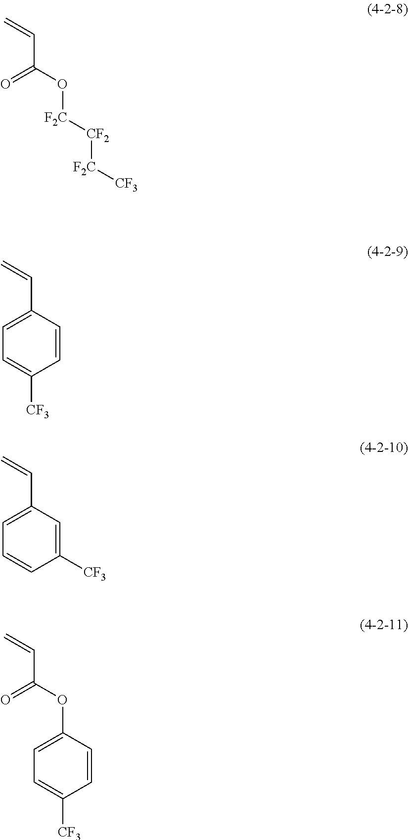
[Chemical formula 63]
A1-O-A2 (S-2)


| TABLE 1 |
| Test for checking insolubility of resist |
| Example 1 | OK | ||
| Example 2 | OK | ||
| Example 3 | OK | ||
| Example 4 | OK | ||
| Example 5 | OK | ||
| Example 6 | OK | ||
| Example 7 | OK | ||
| Example 8 | OK | ||
| Example 9 | OK | ||
| Example 10 | OK | ||
| Example 11 | OK | ||
| Example 12 | OK | ||
| Example 13 | OK | ||
| Example 14 | OK | ||
| Example 15 | OK | ||
| Example 16 | OK | ||
| Example 17 | OK | ||
| Example 18 | OK | ||
| Example 19 | OK | ||
| Example 20 | OK | ||
| Example 21 | OK | ||
| Example 22 | OK | ||
| Example 23 | OK | ||
| Example 24 | OK | ||
| Example 25 | OK | ||
| Example 26 | OK | ||
| Example 27 | OK | ||
| Example 28 | OK | ||
| Example 30 | OK | ||
| Example 29 | OK | ||
| Example 31 | OK | ||
| Example 32 | OK | ||
| Example 33 | OK | ||
| Example 34 | OK | ||
| Example 35 | OK | ||
| Example 36 | OK | ||
| Example 37 | OK | ||
| Example 38 | OK | ||
| Example 39 | OK | ||
| Example 40 | OK | ||
| Example 41 | OK | ||
| Example 42 | OK | ||
| Example 43 | OK | ||
| Example 44 | OK | ||
| Example 45 | OK | ||
| Example 46 | OK | ||
| Example 47 | OK | ||
| Example 48 | OK | ||
| Example 49 | OK | ||
| Example 50 | OK | ||
| Example 51 | OK | ||
| Example 52 | OK | ||
| Example 53 | OK | ||
| Example 54 | OK | ||
| Example 55 | OK | ||
| Example 56 | OK | ||
| Example 57 | OK | ||
| Example 58 | OK | ||
| Example 59 | OK | ||
| Example 60 | OK | ||
| Example 61 | OK | ||
| Example 62 | OK | ||
| Example 63 | OK | ||
| Example 64 | OK | ||
| Example 65 | OK | ||
| Example 66 | OK | ||
| Example 67 | OK | ||
| Example 68 | OK | ||
| Example 69 | OK | ||
| Example 70 | OK | ||
| Example 71 | OK | ||
| Example 72 | OK | ||
| Example 73 | OK | ||
| Example 74 | OK | ||
| Example 75 | OK | ||
| Example 76 | OK | ||
| Example 77 | OK | ||
| Example 78 | OK | ||
| Example 79 | OK | ||
| Example 80 | OK | ||
| Example 81 | OK | ||
| Example 82 | OK | ||
| Example 83 | OK | ||
| Example 84 | OK | ||
| Example 85 | OK | ||
| Example 86 | OK | ||
| Example 87 | OK | ||
| Example 88 | OK | ||
| Comparative Example 1 | NG | ||
| Comparative Example 2 | NG | ||
| Comparative Example 3 | NG | ||
| TABLE 2 |
| Measurement of thickness of film |
| Thickness A (nm) | Thickness B (nm) | ||
| Example 1 | 30 | 0 | ||
| Example 2 | 30 | 0 | ||
| Example 3 | 30 | 0 | ||
| Example 4 | 30 | 0 | ||
| Example 5 | 30 | 0 | ||
| Example 6 | 30 | 0 | ||
| Example 7 | 30 | 0 | ||
| Example 8 | 30 | 0 | ||
| Example 9 | 30 | 0 | ||
| Example 10 | 30 | 0 | ||
| Example 11 | 30 | 0 | ||
| Example 12 | 30 | 0 | ||
| Example 13 | 30 | 0 | ||
| Example 14 | 30 | 0 | ||
| Example 15 | 30 | 0 | ||
| Example 16 | 30 | 0 | ||
| Example 17 | 30 | 0 | ||
| Example 18 | 30 | 0 | ||
| Example 19 | 30 | 0 | ||
| Example 20 | 30 | 0 | ||
| Example 21 | 30 | 0 | ||
| Example 22 | 30 | 0 | ||
| Example 23 | 30 | 0 | ||
| Example 24 | 30 | 0 | ||
| Example 25 | 30 | 0 | ||
| Example 26 | 30 | 0 | ||
| Example 27 | 30 | 0 | ||
| Example 28 | 30 | 0 | ||
| Example 29 | 30 | 0 | ||
| Example 30 | 30 | 0 | ||
| Example 31 | 30 | 0 | ||
| Example 32 | 30 | 0 | ||
| Example 33 | 30 | 0 | ||
| Example 34 | 30 | 0 | ||
| Example 35 | 30 | 0 | ||
| Example 36 | 30 | 0 | ||
| Example 37 | 30 | 0 | ||
| Example 38 | 30 | 0 | ||
| Example 39 | 30 | 0 | ||
| Example 40 | 30 | 0 | ||
| Example 41 | 30 | 0 | ||
| Example 42 | 30 | 0 | ||
| Example 43 | 30 | 0 | ||
| Example 44 | 30 | 0 | ||
| Example 45 | 30 | 0 | ||
| Example 46 | 30 | 0 | ||
| Example 47 | 30 | 0 | ||
| Example 48 | 30 | 0 | ||
| Example 49 | 30 | 0 | ||
| Example 50 | 30 | 0 | ||
| Example 51 | 30 | 0 | ||
| Example 52 | 30 | 0 | ||
| Example 53 | 30 | 0 | ||
| Example 54 | 30 | 0 | ||
| Example 55 | 30 | 0 | ||
| Example 56 | 30 | 0 | ||
| Example 57 | 30 | 0 | ||
| Example 58 | 30 | 0 | ||
| Example 59 | 30 | 0 | ||
| Example 60 | 30 | 0 | ||
| Example 61 | 30 | 0 | ||
| Example 62 | 30 | 0 | ||
| Example 63 | 30 | 0 | ||
| Example 64 | 30 | 0 | ||
| Example 65 | 30 | 0 | ||
| Example 66 | 30 | 0 | ||
| Example 67 | 30 | 0 | ||
| Example 68 | 30 | 0 | ||
| Example 69 | 30 | 0 | ||
| Example 70 | 30 | 0 | ||
| Example 71 | 30 | 0 | ||
| Example 72 | 30 | 0 | ||
| Example 73 | 30 | 0 | ||
| Example 74 | 30 | 0 | ||
| Example 75 | 30 | 0 | ||
| Example 76 | 30 | 0 | ||
| Example 77 | 30 | 0 | ||
| Example 78 | 30 | 0 | ||
| Example 79 | 30 | 0 | ||
| Example 80 | 30 | 0 | ||
| Example 81 | 30 | 0 | ||
| Example 82 | 30 | 0 | ||
| Example 83 | 30 | 0 | ||
| Example 84 | 30 | 0 | ||
| Example 85 | 30 | 0 | ||
| Example 86 | 30 | 0 | ||
| Example 87 | 30 | 0 | ||
| Example 88 | 30 | 0 | ||
| TABLE 3 |
| Measurement of thickness of film |
| Thickness A (nm) | Thickness C (nm) | ||
| Example 1 | 30 | 0 |
| Example 2 | 30 | 0 |
| Example 3 | 30 | 0 |
| Example 4 | 30 | 0 |
| Example 5 | 30 | 0 |
| Example 6 | 30 | 0 |
| Example 7 | 30 | 0 |
| Example 8 | 30 | 0 |
| Example 9 | 30 | 0 |
| Example 10 | 30 | 0 |
| Example 11 | 30 | 0 |
| Example 12 | 30 | 0 |
| Example 13 | 30 | 0 |
| Example 14 | 30 | 0 |
| Example 15 | 30 | 0 |
| Example 16 | 30 | 0 |
| Example 17 | 30 | 0 |
| Example 18 | 30 | 0 |
| Example 19 | 30 | 0 |
| Example 20 | 30 | 0 |
| Example 21 | 30 | 0 |
| Example 22 | 30 | 0 |
| Example 23 | 30 | 0 |
| Example 24 | 30 | 0 |
| Example 25 | 30 | 0 |
| Example 26 | 30 | 0 |
| Example 27 | 30 | 0 |
| Example 28 | 30 | 0 |
| Example 29 | 30 | 0 |
| Example 30 | 30 | 0 |
| Example 31 | 30 | 0 |
| Example 32 | 30 | 0 |
| Example 33 | 30 | 0 |
| Example 34 | 30 | 0 |
| Example 35 | 30 | 0 |
| Example 36 | 30 | 0 |
| Example 37 | 30 | 0 |
| Example 38 | 30 | 0 |
| Example 39 | 30 | 0 |
| Example 40 | 30 | 0 |
| Example 41 | 30 | 0 |
| Example 42 | 30 | 0 |
| Example 43 | 30 | 0 |
| Example 44 | 30 | 0 |
| Example 45 | 30 | 0 |
| Example 46 | 30 | 0 |
| Example 47 | 30 | 0 |
| Example 48 | 30 | 0 |
| Example 49 | 30 | 0 |
| Example 50 | 30 | 0 |
| Example 51 | 30 | 0 |
| Example 52 | 30 | 0 |
| Example 53 | 30 | 0 |
| Example 54 | 30 | 0 |
| Example 55 | 30 | 0 |
| Example 56 | 30 | 0 |
| Example 57 | 30 | 0 |
| Example 58 | 30 | 0 |
| Example 59 | 30 | 0 |
| Example 60 | 30 | 0 |
| Example 61 | 30 | 0 |
| Example 62 | 30 | 0 |
| Example 63 | 30 | 0 |
| Example 64 | 30 | 0 |
| Example 65 | 30 | 0 |
| Example 66 | 30 | 0 |
| Example 67 | 30 | 0 |
| Example 68 | 30 | 0 |
| Example 69 | 30 | 0 |
| Example 70 | 30 | 0 |
| Example 71 | 30 | 0 |
| Example 72 | 30 | 0 |
| Example 73 | 30 | 0 |
| Example 74 | 30 | 0 |
| Example 75 | 30 | 0 |
| Example 76 | 30 | 0 |
| Example 77 | 30 | 0 |
| Example 78 | 30 | 0 |
| Example 79 | 30 | 0 |
| Example 80 | 30 | 0 |
| Example 81 | 30 | 0 |
| Example 82 | 30 | 0 |
| Example 83 | 30 | 0 |
| Example 84 | 30 | 0 |
| Example 85 | 30 | 0 |
| Example 86 | 30 | 0 |
| Example 87 | 30 | 0 |
| Example 88 | 30 | 0 |
| Comparative Example 4 | 30 | 30 |
| TABLE 4 |
| EUV transmission property and DUV cut-off property |
| Transmission | ||||
| Thickness | property | Cut-off property | ||
| (nm) | for EUV light | for DUV light | ||
| Example 1 | 30 | Excellent | Excellent |
| Example 2 | 30 | Excellent | Excellent |
| Example 3 | 30 | Excellent | Excellent |
| Example 4 | 30 | Excellent | Excellent |
| Example 5 | 30 | Excellent | Excellent |
| Example 6 | 30 | Excellent | Excellent |
| Example 7 | 30 | Excellent | Excellent |
| Example 8 | 30 | Excellent | Excellent |
| Example 9 | 30 | Excellent | Excellent |
| Example 10 | 30 | Excellent | Excellent |
| Example 11 | 30 | Excellent | Excellent |
| Example 12 | 30 | Excellent | Excellent |
| Example 13 | 30 | Excellent | Excellent |
| Example 14 | 30 | Excellent | Excellent |
| Example 15 | 30 | Excellent | Excellent |
| Example 16 | 30 | Excellent | Excellent |
| Example 17 | 30 | Excellent | Excellent |
| Example 18 | 30 | Excellent | Excellent |
| Example 19 | 30 | Excellent | Excellent |
| Example 20 | 30 | Excellent | Excellent |
| Example 21 | 30 | Excellent | Excellent |
| Example 22 | 30 | Excellent | Excellent |
| Example 23 | 30 | Excellent | Excellent |
| Example 24 | 30 | Excellent | Excellent |
| Example 25 | 30 | Excellent | Excellent |
| Example 26 | 30 | Excellent | Excellent |
| Example 27 | 30 | Excellent | Excellent |
| Example 28 | 30 | Excellent | Excellent |
| Example 29 | 30 | Excellent | Excellent |
| Example 30 | 30 | Excellent | Excellent |
| Example 31 | 30 | Excellent | Excellent |
| Example 32 | 30 | Excellent | Excellent |
| Example 33 | 30 | Excellent | Excellent |
| Example 34 | 30 | Excellent | Excellent |
| Example 35 | 30 | Excellent | Excellent |
| Example 36 | 30 | Excellent | Excellent |
| Example 37 | 30 | Excellent | Excellent |
| Example 38 | 30 | Excellent | Excellent |
| Example 39 | 30 | Excellent | Excellent |
| Example 40 | 30 | Excellent | Excellent |
| Example 41 | 30 | Excellent | Excellent |
| Example 42 | 30 | Excellent | Excellent |
| Example 43 | 30 | Excellent | Excellent |
| Example 44 | 30 | Excellent | Excellent |
| Example 45 | 30 | Excellent | Excellent |
| Example 46 | 30 | Excellent | Excellent |
| Example 47 | 30 | Excellent | Excellent |
| Example 48 | 30 | Excellent | Excellent |
| Example 49 | 30 | Excellent | Excellent |
| Example 50 | 30 | Excellent | Excellent |
| Example 51 | 30 | Excellent | Excellent |
| Example 52 | 30 | Excellent | Excellent |
| Example 53 | 30 | Excellent | Excellent |
| Example 54 | 30 | Excellent | Excellent |
| Example 55 | 30 | Excellent | Excellent |
| Example 56 | 30 | Excellent | Excellent |
| Example 57 | 30 | Excellent | Excellent |
| Example 58 | 30 | Excellent | Excellent |
| Example 59 | 30 | Excellent | Excellent |
| Example 60 | 30 | Excellent | Excellent |
| Example 61 | 30 | Excellent | Excellent |
| Example 62 | 30 | Excellent | Excellent |
| Example 63 | 30 | Excellent | Excellent |
| Example 64 | 30 | Excellent | Excellent |
| Example 65 | 30 | Excellent | Excellent |
| Example 66 | 30 | Excellent | Excellent |
| Example 67 | 30 | Excellent | Excellent |
| Example 68 | 30 | Excellent | Excellent |
| Example 69 | 30 | Excellent | Excellent |
| Example 70 | 30 | Excellent | Excellent |
| Example 71 | 30 | Excellent | Excellent |
| Example 72 | 30 | Excellent | Excellent |
| Example 73 | 30 | Excellent | Excellent |
| Example 74 | 30 | Excellent | Excellent |
| Example 75 | 30 | Excellent | Excellent |
| Example 76 | 30 | Excellent | Excellent |
| Example 77 | 30 | Excellent | Excellent |
| Example 78 | 30 | Excellent | Excellent |
| Example 79 | 30 | Excellent | Excellent |
| Example 80 | 30 | Excellent | Excellent |
| Example 81 | 30 | Excellent | Excellent |
| Example 82 | 30 | Excellent | Excellent |
| Example 83 | 30 | Excellent | Excellent |
| Example 84 | 30 | Excellent | Excellent |
| Example 85 | 30 | Excellent | Excellent |
| Example 86 | 30 | Excellent | Excellent |
| Example 87 | 30 | Excellent | Excellent |
| Example 88 | 30 | Excellent | Excellent |
| Comparative Example 4 | 30 | Excellent | Bad |
| TABLE 5 |
| Storage stability test |
| Solution immediately | Solution after stored | ||
| after prepared | at 35° C. for 1 month | ||
| Example 15 | OK | OK |
| Comparative Example 5 | OK | NG |
| TABLE 6 |
| Results of evaluation for formation of resist pattern |
| Composition for forming | Cross-sectional | |
| a resist upper-layer film | Critical dimension | form of pattern |
| Example 40 | 29.7 nm | Straight |
| Example 43 | 30.8 nm | Straight |
| Example 44 | 30.7 nm | Straight |
| Comparative Example 6 | 28.5 nm | Straight |
Claims (13)


Applications Claiming Priority (3)
| Application Number | Priority Date | Filing Date | Title |
|---|---|---|---|
| JP2014-150975 | 2014-07-24 | ||
| JP2014150975 | 2014-07-24 | ||
| PCT/JP2015/070909 WO2016013598A1 (en) | 2014-07-24 | 2015-07-23 | Composition for forming upper-layer resist film, and method for manufacturing semiconductor device using said composition |
Publications (2)
| Publication Number | Publication Date |
|---|---|
| US20170205711A1 US20170205711A1 (en) | 2017-07-20 |
| US10042258B2 true US10042258B2 (en) | 2018-08-07 |
Family
ID=55163122
Family Applications (1)
| Application Number | Title | Priority Date | Filing Date |
|---|---|---|---|
| US15/324,542 Active US10042258B2 (en) | 2014-07-24 | 2015-07-23 | Composition for forming a resist upper-layer film and method for producing a semiconductor device using the composition |
Country Status (6)
| Country | Link |
|---|---|
| US (1) | US10042258B2 (en) |
| JP (1) | JP6690535B2 (en) |
| KR (1) | KR102439080B1 (en) |
| CN (1) | CN106575082B (en) |
| TW (1) | TWI712855B (en) |
| WO (1) | WO2016013598A1 (en) |
Cited By (1)
| Publication number | Priority date | Publication date | Assignee | Title |
|---|---|---|---|---|
| US20180252645A1 (en) * | 2015-08-07 | 2018-09-06 | The University Of Queensland | Copolymer and associated layered article, and device-forming method |
Families Citing this family (7)
| Publication number | Priority date | Publication date | Assignee | Title |
|---|---|---|---|---|
| KR102051340B1 (en) * | 2015-09-30 | 2019-12-03 | 후지필름 가부시키가이샤 | Pattern formation method, manufacturing method of an electronic device, and laminated body |
| TWI722135B (en) * | 2016-04-13 | 2021-03-21 | 日商迪愛生股份有限公司 | Novolac resin and resist material |
| CN120802567A (en) * | 2016-04-28 | 2025-10-17 | 日产化学株式会社 | Composition for forming resist underlayer film having improved film density |
| JP7041358B2 (en) * | 2016-06-03 | 2022-03-24 | Jsr株式会社 | Film-forming composition, film, resist underlayer film forming method, patterned substrate manufacturing method and compound |
| KR102215333B1 (en) * | 2017-12-26 | 2021-02-10 | 삼성에스디아이 주식회사 | Resist underlayer composition, and method of forming patterns using the composition |
| US11340528B2 (en) * | 2019-12-11 | 2022-05-24 | Jsr Corporation | Production method of composition for resist top coat layer, method of forming resist pattern, production method of fluorine-containing resin, and method of improving water repellency of resist top coat layer |
| KR20250012666A (en) | 2022-05-26 | 2025-01-24 | 메르크 파텐트 게엠베하 | Developable resist overlayer composition, and method for producing resist overlayer pattern and resist pattern |
Citations (16)
| Publication number | Priority date | Publication date | Assignee | Title |
|---|---|---|---|---|
| JP2006113171A (en) | 2004-10-13 | 2006-04-27 | Fuji Photo Film Co Ltd | Protective film forming composition for liquid immersion exposure and pattern forming method using same |
| WO2007049637A1 (en) | 2005-10-27 | 2007-05-03 | Jsr Corporation | Composition for forming upper film and method for forming photoresist pattern |
| US20070160930A1 (en) | 2006-01-08 | 2007-07-12 | Rohm And Haas Electronic Materials Llc | Coating compositions for photoresists |
| JP2007241109A (en) | 2006-03-10 | 2007-09-20 | Fujifilm Corp | Protective film forming composition and pattern forming method using the same |
| JP2008065304A (en) | 2006-08-11 | 2008-03-21 | Shin Etsu Chem Co Ltd | Resist protective film material and pattern forming method |
| US20120021355A1 (en) | 2010-07-23 | 2012-01-26 | Kim Hyun-Woo | Coating composition for duv filtering, method of forming photoresist pattern using the same and method of fabricating semiconductor device by using the method |
| WO2012053302A1 (en) | 2010-10-21 | 2012-04-26 | 日産化学工業株式会社 | Composition for forming overlaying film for resist for euv lithography |
| WO2013012068A1 (en) | 2011-07-20 | 2013-01-24 | 日産化学工業株式会社 | Thin film formation composition for lithography which contains titanium and silicon |
| JP2013033227A (en) | 2011-06-30 | 2013-02-14 | Fujifilm Corp | Pattern forming method, multilayer resist pattern, multilayer film for development with organic solvent, resist composition, method for manufacturing electronic device, and electronic device |
| US20130059252A1 (en) * | 2011-09-06 | 2013-03-07 | Jsr Corporation | Method for forming resist pattern and composition for forming protective film |
| WO2013051442A1 (en) | 2011-10-06 | 2013-04-11 | 日産化学工業株式会社 | Composition for forming resist upperlayer film for lithography |
| US20130143162A1 (en) | 2011-12-06 | 2013-06-06 | Shin-Etsu Chemical Co., Ltd. | Resist-protective film-forming composition and patterning process |
| US20130143163A1 (en) * | 2011-12-06 | 2013-06-06 | Shin-Etsu Chemical Co., Ltd. | Resist-protective film-forming composition and patterning process |
| JP2013254109A (en) | 2012-06-07 | 2013-12-19 | Az Electronic Materials Mfg Co Ltd | Overlay film forming composition and resist pattern formation method using same |
| US20140080064A1 (en) * | 2012-09-14 | 2014-03-20 | Shin-Etsu Chemical Co., Ltd. | Resist protective film-forming composition and patterning process |
| JP2015011169A (en) | 2013-06-28 | 2015-01-19 | 日産化学工業株式会社 | Composition for forming resist overlay film for lithography and method for manufacturing semiconductor device using the composition |
Family Cites Families (5)
| Publication number | Priority date | Publication date | Assignee | Title |
|---|---|---|---|---|
| JP5453361B2 (en) * | 2011-08-17 | 2014-03-26 | 信越化学工業株式会社 | Silicon-containing resist underlayer film forming composition and pattern forming method |
| JP5836299B2 (en) | 2012-08-20 | 2015-12-24 | 富士フイルム株式会社 | PATTERN FORMATION METHOD, ELECTRON-SENSITIVE OR EXTREME UV-SENSITIVE RESIN COMPOSITION, RESIST FILM, AND METHOD FOR PRODUCING ELECTRONIC DEVICE USING THEM |
| WO2014038483A1 (en) * | 2012-09-07 | 2014-03-13 | 日産化学工業株式会社 | Composition for forming resist upper layer film for lithography and method for manufacturing semiconductor device using same |
| JP6002554B2 (en) | 2012-11-26 | 2016-10-05 | 富士フイルム株式会社 | PATTERN FORMING METHOD AND ELECTRONIC DEVICE MANUFACTURING METHOD USING THE SAME |
| JP5563051B2 (en) * | 2012-12-13 | 2014-07-30 | Azエレクトロニックマテリアルズマニュファクチャリング株式会社 | Upper layer film forming composition and resist pattern forming method using the same |
-
2015
- 2015-07-23 WO PCT/JP2015/070909 patent/WO2016013598A1/en not_active Ceased
- 2015-07-23 KR KR1020177000339A patent/KR102439080B1/en active Active
- 2015-07-23 US US15/324,542 patent/US10042258B2/en active Active
- 2015-07-23 TW TW104123889A patent/TWI712855B/en active
- 2015-07-23 CN CN201580040881.2A patent/CN106575082B/en active Active
- 2015-07-23 JP JP2016535964A patent/JP6690535B2/en active Active
Patent Citations (31)
| Publication number | Priority date | Publication date | Assignee | Title |
|---|---|---|---|---|
| JP2006113171A (en) | 2004-10-13 | 2006-04-27 | Fuji Photo Film Co Ltd | Protective film forming composition for liquid immersion exposure and pattern forming method using same |
| US8076053B2 (en) | 2005-10-27 | 2011-12-13 | Jsr Corporation | Upper layer-forming composition and photoresist patterning method |
| WO2007049637A1 (en) | 2005-10-27 | 2007-05-03 | Jsr Corporation | Composition for forming upper film and method for forming photoresist pattern |
| JP2012103738A (en) | 2005-10-27 | 2012-05-31 | Jsr Corp | Upper layer film-forming composition and method for forming photoresist pattern |
| US8435718B2 (en) | 2005-10-27 | 2013-05-07 | Jsr Corporation | Upper layer-forming composition and photoresist patterning method |
| US20120028198A1 (en) | 2005-10-27 | 2012-02-02 | Jsr Corporation | Upper layer-forming composition and photoresist patterning method |
| US20100003615A1 (en) | 2005-10-27 | 2010-01-07 | Jsr Corporation | Upper layer-forming composition and photoresist patterning method |
| JP2007219504A (en) | 2006-01-08 | 2007-08-30 | Rohm & Haas Electronic Materials Llc | Coating composition for photoresist |
| US20110143281A1 (en) | 2006-01-08 | 2011-06-16 | Rohm And Haas Electronic Materials Llc | Coating compositions for photoresists |
| US20070160930A1 (en) | 2006-01-08 | 2007-07-12 | Rohm And Haas Electronic Materials Llc | Coating compositions for photoresists |
| JP2007241109A (en) | 2006-03-10 | 2007-09-20 | Fujifilm Corp | Protective film forming composition and pattern forming method using the same |
| JP2008065304A (en) | 2006-08-11 | 2008-03-21 | Shin Etsu Chem Co Ltd | Resist protective film material and pattern forming method |
| US20120021355A1 (en) | 2010-07-23 | 2012-01-26 | Kim Hyun-Woo | Coating composition for duv filtering, method of forming photoresist pattern using the same and method of fabricating semiconductor device by using the method |
| US20130209940A1 (en) | 2010-10-21 | 2013-08-15 | Nissan Chemical Industries, Ltd. | Composition for forming resist overlayer film for euv lithography |
| WO2012053302A1 (en) | 2010-10-21 | 2012-04-26 | 日産化学工業株式会社 | Composition for forming overlaying film for resist for euv lithography |
| US20140113223A1 (en) | 2011-06-30 | 2014-04-24 | Fujifilm Corporation | Pattern forming method, multi-layered resist pattern, multi-layered film for organic solvent development, resist composition, method for manufacturing electronic device, and electronic device |
| JP2013033227A (en) | 2011-06-30 | 2013-02-14 | Fujifilm Corp | Pattern forming method, multilayer resist pattern, multilayer film for development with organic solvent, resist composition, method for manufacturing electronic device, and electronic device |
| US20140120730A1 (en) | 2011-07-20 | 2014-05-01 | Nissan Chemical Industries, Ltd. | Thin film forming composition for lithography containing titanium and silicon |
| WO2013012068A1 (en) | 2011-07-20 | 2013-01-24 | 日産化学工業株式会社 | Thin film formation composition for lithography which contains titanium and silicon |
| JP2013228663A (en) | 2011-09-06 | 2013-11-07 | Jsr Corp | Method for forming resist pattern and composition for forming protective film |
| US20130059252A1 (en) * | 2011-09-06 | 2013-03-07 | Jsr Corporation | Method for forming resist pattern and composition for forming protective film |
| US9052600B2 (en) | 2011-09-06 | 2015-06-09 | Jsr Corporation | Method for forming resist pattern and composition for forming protective film |
| WO2013051442A1 (en) | 2011-10-06 | 2013-04-11 | 日産化学工業株式会社 | Composition for forming resist upperlayer film for lithography |
| US20140255847A1 (en) | 2011-10-06 | 2014-09-11 | Nissan Chemical Industries, Ltd. | Resist overlayer film forming composition for lithography |
| JP2013120194A (en) | 2011-12-06 | 2013-06-17 | Shin Etsu Chem Co Ltd | Resist protective film material and pattern forming method |
| US20130143163A1 (en) * | 2011-12-06 | 2013-06-06 | Shin-Etsu Chemical Co., Ltd. | Resist-protective film-forming composition and patterning process |
| US20130143162A1 (en) | 2011-12-06 | 2013-06-06 | Shin-Etsu Chemical Co., Ltd. | Resist-protective film-forming composition and patterning process |
| JP2013254109A (en) | 2012-06-07 | 2013-12-19 | Az Electronic Materials Mfg Co Ltd | Overlay film forming composition and resist pattern formation method using same |
| US20150140490A1 (en) | 2012-06-07 | 2015-05-21 | Az Electronic Materials (Luxembourg) S.A.R.L. | Overlay film forming composition and resist pattern formation method using same |
| US20140080064A1 (en) * | 2012-09-14 | 2014-03-20 | Shin-Etsu Chemical Co., Ltd. | Resist protective film-forming composition and patterning process |
| JP2015011169A (en) | 2013-06-28 | 2015-01-19 | 日産化学工業株式会社 | Composition for forming resist overlay film for lithography and method for manufacturing semiconductor device using the composition |
Non-Patent Citations (1)
| Title |
|---|
| Oct. 13, 2015 International Search Report issued in International Patent Application No. PCT/JP2015/070909. |
Cited By (1)
| Publication number | Priority date | Publication date | Assignee | Title |
|---|---|---|---|---|
| US20180252645A1 (en) * | 2015-08-07 | 2018-09-06 | The University Of Queensland | Copolymer and associated layered article, and device-forming method |
Also Published As
| Publication number | Publication date |
|---|---|
| JPWO2016013598A1 (en) | 2017-04-27 |
| JP6690535B2 (en) | 2020-04-28 |
| CN106575082A (en) | 2017-04-19 |
| TWI712855B (en) | 2020-12-11 |
| CN106575082B (en) | 2020-09-25 |
| WO2016013598A1 (en) | 2016-01-28 |
| US20170205711A1 (en) | 2017-07-20 |
| TW201621462A (en) | 2016-06-16 |
| KR102439080B1 (en) | 2022-09-01 |
| KR20170035883A (en) | 2017-03-31 |
Similar Documents
| Publication | Publication Date | Title |
|---|---|---|
| US10042258B2 (en) | Composition for forming a resist upper-layer film and method for producing a semiconductor device using the composition | |
| US9494864B2 (en) | Resist overlayer film forming composition for lithography and method for manufacturing semiconductor device using the same | |
| KR102200511B1 (en) | Composition for forming upper layer film of lithographic resist and method for producing semiconductor device using same | |
| US9977331B2 (en) | Resist overlayer film forming composition and method for producing semiconductor device including the same | |
| US10133178B2 (en) | Coating liquid for resist pattern coating | |
| JP6119983B2 (en) | Composition for forming resist upper layer film for lithography and method for manufacturing semiconductor device using the same | |
| JP2014174329A (en) | Composition for forming resist overlay film for lithography and method for manufacturing semiconductor device using the composition | |
| JPWO2013051442A1 (en) | Composition for forming resist upper layer film for lithography | |
| CN118355328A (en) | Resist underlayer film-forming composition containing a polycyclic aromatic polymer | |
| US20230244148A1 (en) | Euv resist underlayer film-forming composition | |
| CN118215886A (en) | Alkyl group-containing composition for forming a resist underlayer film |
Legal Events
| Date | Code | Title | Description |
|---|---|---|---|
| AS | Assignment |
Owner name: NISSAN CHEMICAL INDUSTRIES, LTD., JAPAN Free format text: ASSIGNMENT OF ASSIGNORS INTEREST;ASSIGNORS:FUJITANI, NORIAKI;ENDO, TAKAFUMI;SAKAMOTO, RIKIMARU;REEL/FRAME:040875/0145 Effective date: 20161226 |
|
| STCF | Information on status: patent grant |
Free format text: PATENTED CASE |
|
| MAFP | Maintenance fee payment |
Free format text: PAYMENT OF MAINTENANCE FEE, 4TH YEAR, LARGE ENTITY (ORIGINAL EVENT CODE: M1551); ENTITY STATUS OF PATENT OWNER: LARGE ENTITY Year of fee payment: 4 |
|
| MAFP | Maintenance fee payment |
Free format text: PAYMENT OF MAINTENANCE FEE, 8TH YEAR, LARGE ENTITY (ORIGINAL EVENT CODE: M1552); ENTITY STATUS OF PATENT OWNER: LARGE ENTITY Year of fee payment: 8 |