US10042208B2 - Liquid crystal alignment method, pixel structure, display panel and display device - Google Patents
Liquid crystal alignment method, pixel structure, display panel and display device Download PDFInfo
- Publication number
- US10042208B2 US10042208B2 US15/502,168 US201615502168A US10042208B2 US 10042208 B2 US10042208 B2 US 10042208B2 US 201615502168 A US201615502168 A US 201615502168A US 10042208 B2 US10042208 B2 US 10042208B2
- Authority
- US
- United States
- Prior art keywords
- liquid crystal
- electrode lines
- substrate
- alignment
- convex lens
- Prior art date
- Legal status (The legal status is an assumption and is not a legal conclusion. Google has not performed a legal analysis and makes no representation as to the accuracy of the status listed.)
- Expired - Fee Related, expires
Links
- 239000004973 liquid crystal related substance Substances 0.000 title claims abstract description 122
- 238000000034 method Methods 0.000 title claims abstract description 42
- 239000000758 substrate Substances 0.000 claims abstract description 63
- 230000001678 irradiating effect Effects 0.000 claims abstract description 11
- 238000000059 patterning Methods 0.000 claims description 5
- 230000000694 effects Effects 0.000 abstract description 4
- 230000002708 enhancing effect Effects 0.000 abstract description 3
- 238000005516 engineering process Methods 0.000 abstract description 2
- 239000010408 film Substances 0.000 description 32
- 230000003287 optical effect Effects 0.000 description 16
- 230000008901 benefit Effects 0.000 description 3
- 230000005684 electric field Effects 0.000 description 3
- 239000010409 thin film Substances 0.000 description 3
- 239000005357 flat glass Substances 0.000 description 2
- 238000002834 transmittance Methods 0.000 description 2
- 230000015572 biosynthetic process Effects 0.000 description 1
- 238000006243 chemical reaction Methods 0.000 description 1
- 239000003795 chemical substances by application Substances 0.000 description 1
- 239000011248 coating agent Substances 0.000 description 1
- 238000000576 coating method Methods 0.000 description 1
- 239000013078 crystal Substances 0.000 description 1
- 230000007812 deficiency Effects 0.000 description 1
- 238000005530 etching Methods 0.000 description 1
- 238000011049 filling Methods 0.000 description 1
- 238000001914 filtration Methods 0.000 description 1
- 238000012986 modification Methods 0.000 description 1
- 230000004048 modification Effects 0.000 description 1
- 238000001782 photodegradation Methods 0.000 description 1
- 238000007699 photoisomerization reaction Methods 0.000 description 1
- 230000000704 physical effect Effects 0.000 description 1
- 229920006254 polymer film Polymers 0.000 description 1
- 238000006467 substitution reaction Methods 0.000 description 1
- 239000013598 vector Substances 0.000 description 1
Images


Classifications
-
- G—PHYSICS
- G02—OPTICS
- G02F—OPTICAL DEVICES OR ARRANGEMENTS FOR THE CONTROL OF LIGHT BY MODIFICATION OF THE OPTICAL PROPERTIES OF THE MEDIA OF THE ELEMENTS INVOLVED THEREIN; NON-LINEAR OPTICS; FREQUENCY-CHANGING OF LIGHT; OPTICAL LOGIC ELEMENTS; OPTICAL ANALOGUE/DIGITAL CONVERTERS
- G02F1/00—Devices or arrangements for the control of the intensity, colour, phase, polarisation or direction of light arriving from an independent light source, e.g. switching, gating or modulating; Non-linear optics
- G02F1/01—Devices or arrangements for the control of the intensity, colour, phase, polarisation or direction of light arriving from an independent light source, e.g. switching, gating or modulating; Non-linear optics for the control of the intensity, phase, polarisation or colour
- G02F1/13—Devices or arrangements for the control of the intensity, colour, phase, polarisation or direction of light arriving from an independent light source, e.g. switching, gating or modulating; Non-linear optics for the control of the intensity, phase, polarisation or colour based on liquid crystals, e.g. single liquid crystal display cells
- G02F1/133—Constructional arrangements; Operation of liquid crystal cells; Circuit arrangements
- G02F1/1333—Constructional arrangements; Manufacturing methods
- G02F1/1337—Surface-induced orientation of the liquid crystal molecules, e.g. by alignment layers
- G02F1/133753—Surface-induced orientation of the liquid crystal molecules, e.g. by alignment layers with different alignment orientations or pretilt angles on a same surface, e.g. for grey scale or improved viewing angle
-
- G—PHYSICS
- G02—OPTICS
- G02F—OPTICAL DEVICES OR ARRANGEMENTS FOR THE CONTROL OF LIGHT BY MODIFICATION OF THE OPTICAL PROPERTIES OF THE MEDIA OF THE ELEMENTS INVOLVED THEREIN; NON-LINEAR OPTICS; FREQUENCY-CHANGING OF LIGHT; OPTICAL LOGIC ELEMENTS; OPTICAL ANALOGUE/DIGITAL CONVERTERS
- G02F1/00—Devices or arrangements for the control of the intensity, colour, phase, polarisation or direction of light arriving from an independent light source, e.g. switching, gating or modulating; Non-linear optics
- G02F1/01—Devices or arrangements for the control of the intensity, colour, phase, polarisation or direction of light arriving from an independent light source, e.g. switching, gating or modulating; Non-linear optics for the control of the intensity, phase, polarisation or colour
- G02F1/13—Devices or arrangements for the control of the intensity, colour, phase, polarisation or direction of light arriving from an independent light source, e.g. switching, gating or modulating; Non-linear optics for the control of the intensity, phase, polarisation or colour based on liquid crystals, e.g. single liquid crystal display cells
- G02F1/133—Constructional arrangements; Operation of liquid crystal cells; Circuit arrangements
- G02F1/1333—Constructional arrangements; Manufacturing methods
- G02F1/1335—Structural association of cells with optical devices, e.g. polarisers or reflectors
-
- G—PHYSICS
- G02—OPTICS
- G02F—OPTICAL DEVICES OR ARRANGEMENTS FOR THE CONTROL OF LIGHT BY MODIFICATION OF THE OPTICAL PROPERTIES OF THE MEDIA OF THE ELEMENTS INVOLVED THEREIN; NON-LINEAR OPTICS; FREQUENCY-CHANGING OF LIGHT; OPTICAL LOGIC ELEMENTS; OPTICAL ANALOGUE/DIGITAL CONVERTERS
- G02F1/00—Devices or arrangements for the control of the intensity, colour, phase, polarisation or direction of light arriving from an independent light source, e.g. switching, gating or modulating; Non-linear optics
- G02F1/01—Devices or arrangements for the control of the intensity, colour, phase, polarisation or direction of light arriving from an independent light source, e.g. switching, gating or modulating; Non-linear optics for the control of the intensity, phase, polarisation or colour
- G02F1/13—Devices or arrangements for the control of the intensity, colour, phase, polarisation or direction of light arriving from an independent light source, e.g. switching, gating or modulating; Non-linear optics for the control of the intensity, phase, polarisation or colour based on liquid crystals, e.g. single liquid crystal display cells
- G02F1/133—Constructional arrangements; Operation of liquid crystal cells; Circuit arrangements
- G02F1/1333—Constructional arrangements; Manufacturing methods
- G02F1/1337—Surface-induced orientation of the liquid crystal molecules, e.g. by alignment layers
- G02F1/13378—Surface-induced orientation of the liquid crystal molecules, e.g. by alignment layers by treatment of the surface, e.g. embossing, rubbing or light irradiation
- G02F1/133788—Surface-induced orientation of the liquid crystal molecules, e.g. by alignment layers by treatment of the surface, e.g. embossing, rubbing or light irradiation by light irradiation, e.g. linearly polarised light photo-polymerisation
-
- G—PHYSICS
- G02—OPTICS
- G02F—OPTICAL DEVICES OR ARRANGEMENTS FOR THE CONTROL OF LIGHT BY MODIFICATION OF THE OPTICAL PROPERTIES OF THE MEDIA OF THE ELEMENTS INVOLVED THEREIN; NON-LINEAR OPTICS; FREQUENCY-CHANGING OF LIGHT; OPTICAL LOGIC ELEMENTS; OPTICAL ANALOGUE/DIGITAL CONVERTERS
- G02F1/00—Devices or arrangements for the control of the intensity, colour, phase, polarisation or direction of light arriving from an independent light source, e.g. switching, gating or modulating; Non-linear optics
- G02F1/01—Devices or arrangements for the control of the intensity, colour, phase, polarisation or direction of light arriving from an independent light source, e.g. switching, gating or modulating; Non-linear optics for the control of the intensity, phase, polarisation or colour
- G02F1/13—Devices or arrangements for the control of the intensity, colour, phase, polarisation or direction of light arriving from an independent light source, e.g. switching, gating or modulating; Non-linear optics for the control of the intensity, phase, polarisation or colour based on liquid crystals, e.g. single liquid crystal display cells
- G02F1/133—Constructional arrangements; Operation of liquid crystal cells; Circuit arrangements
- G02F1/1333—Constructional arrangements; Manufacturing methods
- G02F1/1337—Surface-induced orientation of the liquid crystal molecules, e.g. by alignment layers
- G02F1/133753—Surface-induced orientation of the liquid crystal molecules, e.g. by alignment layers with different alignment orientations or pretilt angles on a same surface, e.g. for grey scale or improved viewing angle
- G02F1/133757—Surface-induced orientation of the liquid crystal molecules, e.g. by alignment layers with different alignment orientations or pretilt angles on a same surface, e.g. for grey scale or improved viewing angle with different alignment orientations
-
- G—PHYSICS
- G02—OPTICS
- G02F—OPTICAL DEVICES OR ARRANGEMENTS FOR THE CONTROL OF LIGHT BY MODIFICATION OF THE OPTICAL PROPERTIES OF THE MEDIA OF THE ELEMENTS INVOLVED THEREIN; NON-LINEAR OPTICS; FREQUENCY-CHANGING OF LIGHT; OPTICAL LOGIC ELEMENTS; OPTICAL ANALOGUE/DIGITAL CONVERTERS
- G02F1/00—Devices or arrangements for the control of the intensity, colour, phase, polarisation or direction of light arriving from an independent light source, e.g. switching, gating or modulating; Non-linear optics
- G02F1/01—Devices or arrangements for the control of the intensity, colour, phase, polarisation or direction of light arriving from an independent light source, e.g. switching, gating or modulating; Non-linear optics for the control of the intensity, phase, polarisation or colour
- G02F1/13—Devices or arrangements for the control of the intensity, colour, phase, polarisation or direction of light arriving from an independent light source, e.g. switching, gating or modulating; Non-linear optics for the control of the intensity, phase, polarisation or colour based on liquid crystals, e.g. single liquid crystal display cells
- G02F1/133—Constructional arrangements; Operation of liquid crystal cells; Circuit arrangements
- G02F1/1333—Constructional arrangements; Manufacturing methods
- G02F1/1343—Electrodes
- G02F1/134309—Electrodes characterised by their geometrical arrangement
Definitions
- the present disclosure relates to the field of display technologies, and particularly to a liquid crystal alignment method, a pixel structure, a display panel and a display device.
- a liquid crystal display is a kind of widely used flat panel display.
- the liquid crystal display achieves gray-scale display mainly by modulating the light field intensity of the backlight via a liquid crystal switch, while achieving color display in connection with the color filtering function of an optical filter.
- the LCD has a variety of display modes, among which the Fringe Field Switching (FFS) mode and the Advanced Super Dimension Switch (ADS) mode are display modes having advantages such as high contrast, high transmittance, wide viewing angle and the like.
- FFS Fringe Field Switching
- ADS Advanced Super Dimension Switch
- liquid crystal molecules are rotated within a horizontal plane on the surface of the electrode, there is a great difference in the birefringence between the liquid crystal molecules, moreover, the liquid crystal molecules are arranged in a direction perpendicular to the major axes of the liquid crystal molecules, there is a great difference in the optical path difference (i.e. optical retardation) at different viewing angles (i.e. upper viewing angle, lower viewing angle, left viewing angle and right viewing angle), thus the problem of color cast is serious at a large viewing angle.
- the incident light parallel to the major axis direction of the liquid crystal molecules is bluish, and the incident light perpendicular to the major axis direction of the liquid crystal molecules is yellowish. Therefore, there is a need to address the problem of color cast in the ADS mode.
- the problem of color cast in the ADS mode is usually solved by dual-domain technique.
- the structure of the electrode line (which is used to form an electric field that controls the deflection of liquid crystal molecules) is designed as two portions within one and the same pixel structure (the pixel structure is a dual-domain pixel structure).
- the two portions are an upper portion and a lower portion, which are symmetric to each other.
- the electrode lines the liquid crystal molecules in the upper portion and the liquid crystal molecules in the lower portion are respectively deflected towards two directions, such that a locally symmetric structure is formed within the entire pixel structure.
- the color of the incident light parallel to the major axis direction of the liquid crystal molecules and the color of the incident light perpendicular to the major axis direction of the liquid crystal molecules can be partially canceled out, improving the problem of color cast.
- the liquid crystal molecules in the above pixel structure are arranged in accordance with the major axis, thus the influences resulting from the difference in the birefringence between the liquid crystal molecules and the difference in the optical retardation cannot be completely eliminated, and the color cast for the pixel structure at different viewing angles is still high, especially at the upper viewing angle and the lower viewing angle, hence the quality of the displayed picture is poor.
- embodiments of the invention provide a liquid crystal alignment method, a pixel structure, a display panel, and a display device.
- An embodiment of the invention provides a liquid crystal alignment method, the method may comprise the following steps:
- the alignment film comprising a plurality of annular grooves nested from inside to outside, an orthographic projection of the plurality of annular grooves on a layer where the annular electrode lines reside being located in a spacing region of the at least two spaced apart annular electrode lines; and adding a plurality of liquid crystal molecules into the alignment structure such that the plurality of liquid crystal molecules enclose a plurality of annular structures nested from inside to outside.
- each of the annular grooves may have a width of 10 ⁇ m to 200 ⁇ m.
- a total exposure of the light source may be 1000 mJ/cm 2 to 3000 mJ/cm 2
- a distance between the light source and the first substrate may be 1 mm to 10 mm
- a radius of curvature of the convex lens may be 5 m.
- the step of forming at least two spaced apart annular electrode lines on a first substrate may comprise forming, on the first substrate, the at least two spaced apart annular electrode lines by patterning process.
- the light source may be an ultraviolet point light source of linearly polarized light.
- the pixel structure may comprise at least two spaced apart annular electrode lines and an alignment structure above a layer where the annular electrode lines reside.
- the alignment structure may comprise a plurality of annular grooves nested from inside to outside, and an orthographic projection of the plurality of annular grooves on the layer where the annular electrode lines reside is located in a spacing region of the at least two spaced apart annular electrode lines.
- the at least two spaced apart annular electrode lines may be provided on the first substrate.
- liquid crystal molecules may enclose within the alignment structure a plurality of annular structures nested from inside to outside.
- the alignment structure may be formed by the following steps: forming an alignment film on the layer where the annular electrode lines reside, disposing a convex lens above the formed alignment film, the convex lens being enclosed by a flat surface and a convex surface, a center point of the convex surface of the convex lens being in contact with the alignment film, irradiating the flat surface of the convex lens with a light source so that the alignment film is formed into the alignment structure.
- each of the annular grooves may have a width of 10 ⁇ m to 200 ⁇ m.
- a total exposure of the light source is 1000 mJ/cm 2 to 3000 mJ/cm 2
- a distance between the light source and the first substrate is 1 mm to 10 mm
- a radius of curvature of the convex lens is 5 m.
- the light source may be an ultraviolet point light source of linearly polarized light.
- the display panel may comprise a first substrate, a second substrate, and a liquid crystal layer between the first substrate and the second substrate.
- the first substrate may be provided with the pixel structure according to any one of the aforegoing embodiments.
- a further embodiment of the present invention provides a display device which may comprise the display panel described in the aforegoing embodiments.
- an alignment film is formed on the annular electrode lines, a convex lens is disposed on the first substrate where the alignment film is formed, and the flat surface of the convex lens is irradiated with a light source, such that the alignment film is formed into an alignment structure comprising a plurality of annular grooves nested from inside to outside, and finally a plurality of liquid crystal modules enclose a plurality of annular structures nested from inside to outside. Therefore, as compared to the prior art, the liquid crystal molecules are not arranged along a direction perpendicular to the major axes thereof, that is, the liquid crystal molecules are no longer arranged in accordance with a single direction. Consequently, the liquid crystal alignment method can alleviate or eliminate the influences resulting from the difference in the birefringence between the liquid crystal molecules and the difference in optical retardation, thereby further improving the color cast at different viewing angles and enhancing the quality of the displayed picture.
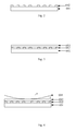
- FIG. 1 is a flow chart of a liquid crystal alignment method provided by an embodiment of the present invention
- FIG. 2 is a side view of a first substrate where at least two spaced apart annular electrode lines are formed as provided by an embodiment of the invention
- FIG. 3 is a side view of a first substrate where an alignment film is formed as provided by an embodiment of the invention
- FIG. 4 is a schematic view showing a structure in which a convex lens is disposed on the first substrate as provided by an embodiment of the present invention
- FIG. 5 illustrates an alignment structure provided by an embodiment of the present invention
- FIG. 6 is a schematic view of a pixel structure provided by an embodiment of the present invention.
- FIG. 7 is a schematic view of a Newton ring
- FIG. 8 illustrates creation of an interference phenomenon
- FIG. 9 is a schematic view of a conventional single-domain pixel structure
- FIG. 10 is a schematic view of a conventional dual-domain pixel structure.
- Embodiments of the invention provide a liquid crystal alignment method. As shown in FIG. 1 , the liquid crystal alignment method comprises the following steps:
- step 101 forming, on a first substrate, at least two spaced apart annular electrode lines;
- step 102 forming an alignment film on the first substrate on which the at least two spaced apart annular electrode lines are formed;
- step 103 disposing a convex lens on the first substrate on which the alignment film is formed, the convex lens being enclosed by a flat surface and a convex surface, and the center point of the convex surface of the convex lens being in contact with the alignment film;
- step 104 irradiating the flat surface of the convex lens with a light source such that the alignment film is formed into an alignment structure, the alignment structure comprises a plurality of annular grooves nested from inside to outside, and the orthographic projection of the plurality of annular grooves on the layer where the annular electrode lines reside is located in a spacing region of the at least two spaced apart annular electrode lines;
- step 105 adding a plurality of liquid crystal molecules into the alignment structure such that the plurality of liquid crystal molecules enclose a plurality of annular structures nested from inside to outside.
- FIG. 2 shows a side view of the first substrate where at least two spaced apart annular electrode lines are formed.
- the at least two spaced apart annular electrode lines may be formed on the first substrate by patterning process.
- the process of forming the annular electrode lines may include processes such as coating, exposure, development, etching, and the like.
- an alignment film 003 is formed on the first substrate 001 where the at least two annular electrode lines 002 disposed at intervals are formed.
- the process of forming an alignment film is known to those skilled in the art and will not be described in detail herein.
- a convex lens 004 is arranged on the first substrate 001 where the alignment film 003 is formed.
- the convex lens 004 is enclosed by a flat surface a and a convex surface b, and the center point of the convex surface b of the convex lens 004 is in contact with the alignment film 003 .
- Reference numeral 002 in FIG. 4 denotes an annular electrode line.
- the flat surface a of the convex lens is irradiated with a light source such that the alignment film is formed into an alignment structure 006 .
- the alignment structure 006 comprises a plurality of annular grooves 007 nested from inside to outside, and the orthographic projection of the plurality of annular grooves on the layer where the annular electrode lines reside is located in a spacing region of the at least two spaced apart annular electrode lines.
- reference numeral 001 denotes a first substrate and reference numeral 002 denotes an annular electrode line.
- FIG. 6 shows a top view of a pixel structure that utilizes the liquid crystal alignment method proposed herein.
- a plurality of liquid crystal molecules 10 within the pixel structure enclose a plurality of annular structures nested from inside to outside.
- the liquid crystal molecules are not deflected and are in an off state. After the annular electrode lines are energized, the liquid crystal molecules will be deflected and in an on state.
- the deflection direction of the liquid crystal molecules may be the direction indicated in FIG. 6 .
- each annular groove may have a width of 10 ⁇ m to 200 ⁇ m to meet the requirements of the displayed picture and improve the quality of the displayed picture.
- the total exposure of the light source that irradiates the convex lens may be 1000 mJ/cm 2 to 3000 mJ/cm 2
- the distance between the light source and the first substrate may be 1 mm to 10 mm
- the radius of curvature of the convex lens may be 5 m.
- the embodiment of the invention enables each annular groove to have a width of 10 ⁇ m to 200 ⁇ m by controlling the total exposure of the light source, the distance between the light source and the first substrate and the size of the convex lens, thereby improving the quality of the displayed picture.
- the light source for irradiating the convex lens may be an ultraviolet point light source of linearly polarized light.
- the liquid crystal alignment is carried out by a photoalignment technique.
- the photoalignment technique is a non-contact type alignment technique, which irradiates a polymer film (i.e.
- an alignment film having a photosensitive agent by using an ultraviolet point light source of linearly polarized light, and performs alignment for specific regions by means of reactions such as photocrosslinking, photodegradation, photoisomerization and so on, preventing the surface of the alignment film from being contaminated.
- the Newton ring in physics is a thin film interference phenomenon based on the equal thickness interference principle. For example, assuming that the convex surface of a convex lens having a large radius of curvature is brought into contact with a flat glass, in daylight or upon irradiation with white light, it can be seen that the contact point of the convex lens and the flat glass is a dark spot, around which are some colored circular rings alternative with brightness and darkness. Upon irradiation with monochromatic light, then some monochromatic circles alternative with brightness and darkness are presented, as shown in FIG. 7 .
- a convex lens having a relatively large radius of curvature is disposed on the first substrate where the alignment film is formed, and the flat surface of the convex lens is irradiated with a light source. Since there is an thin air layer between the convex surface of the convex lens and the upper surface of the first substrate, and the thickness of the thin air layer gradually increases from the center to the edge, the light reflected by the upper surface and the lower surface of the thin air layer encounters at the convex surface of the convex lens, creating an interference phenomenon. As shown in FIG.
- the light reflected by the upper surface and the lower surface of the thin air layer encounters at a point A on the convex surface of the convex lens, creating an interference phenomenon. Therefore, after irradiating the flat surface of the convex lens with a light source, different light intensities will be generated to induce the alignment film to form an alignment structure.
- Adding a plurality of liquid crystal molecules into the formed alignment structure enables the plurality of liquid crystal molecules to enclose a plurality of annular structures nested from inside to outside. Finally, the liquid crystal molecules can be rotated under the effect of the electrode lines, so that they can act as light valves.
- At least two spaced apart annular electrode lines may be formed on the first substrate by patterning process. This formation process is relatively simple.
- an annular color resistance structure on the surface of a color filter (CF) substrate matching with the thin film transistor (TFT) substrate can also be implemented by means of patterning process, which will not be described in detail herein.
- the structure of the liquid crystal molecules has a characteristic of anisotropy, thus the resulting photoelectric effect varies with different directions, that is, the liquid crystal molecules have anisotropy in photoelectric properties such as dielectric constant, refraction coefficient (i.e. refractive index), and the like.
- the refraction coefficient since the liquid crystal molecules are mostly rod-shaped or butterfly-like molecules, the physical properties in the direction parallel to or perpendicular to the major axes of liquid crystal molecules would be somewhat different, and the liquid crystal molecules are also called anisotropic crystals.
- the refraction coefficient can be divided into vectors in two directions, which are n// and n ⁇ respectively.
- liquid crystal molecules having a single optical axis they originally have definitions of two different refraction coefficients, one of which is no, the other is ne.
- the “no” refers to the refraction coefficient of ordinary light, the electric field component of the light wave of ordinary light is perpendicular to the optical axis.
- the “ne” refers to the refraction coefficient of extraordinary light, and the electric field component of the light wave of extraordinary light is parallel to the optical axis.
- the birefringence ⁇ n ne ⁇ no, which refers to a difference between the two refraction coefficients.
- the birefringence is greater than zero when the traveling direction of light is perpendicular to the major axes of the liquid crystal molecules, and the birefringence is less than zero when the traveling direction of light is parallel to the major axes of the liquid crystal molecules.
- FIG. 9 shows a schematic view of a single-domain pixel structure in the ADS mode in the prior art.
- the incident light parallel to the major axis direction of the liquid crystal molecule 100 is bluish, and the incident light perpendicular to the major axis direction of the liquid crystal molecule is yellowish.
- reference numeral 30 denotes an electrode line and reference numeral 40 denotes a thin film transistor (TFT).
- TFT thin film transistor
- the prior art usually employs a dual-domain pixel structure. As shown in FIG. 10 , in one and the same dual-domain pixel structure, the structure of the electrode line is designed as two portions. These two portions are an upper portion and a lower portion, which are symmetric to each other. Driven by the electrode lines, liquid crystal molecules 200 in the upper portion and liquid crystal molecules 300 in the lower portion are respectively deflected towards two directions, so that a locally symmetric structure is formed within the entire dual-domain pixel structure.
- the dual-domain pixel structure shown in FIG. 10 can mitigate the problem of color cast only at a specific viewing angle and in a specific range. Generally, the color cast at the left and right viewing angles is lower, and the color cast at the upper and lower viewing angles is higher. In addition, the two domains of this dual-domain pixel structure overlap in the transitional region (the region indicated by reference numeral 50 in FIG. 10 ), such that a liquid crystal dark region is easily formed, reducing the transmittance.
- this dual-domain pixel structure cannot fundamentally eliminate the influences resulting from the difference in the refractive index between the liquid crystal molecules and the difference in the optical retardation, which consequently cannot solve the problem of color cast completely.
- the liquid crystal alignment method enables a plurality of liquid crystal molecules to enclose a plurality of annular structures nested from inside to outside, and the annularly symmetric liquid crystal molecules have a better improvement effect for color cast, because when the pixels are viewed from respective directions, the overall orientations of the plurality of liquid crystal molecules within the pixel are basically consistent, the birefringences and the optical retardation of the liquid crystal molecules are also substantially the same, the liquid crystal molecules are no longer arranged in accordance with a single direction, and the liquid crystal molecules can realize 360° symmetry within the entire pixel plane. Accordingly, the liquid crystal alignment method can alleviate or eliminate the influences resulting from the difference in the birefringence between the liquid crystal molecules and the difference in the optical retardation, which may further improve the color cast at different viewing angles and enhance the quality of the displayed picture.
- the liquid crystal alignment method comprises forming an alignment film on the annular electrode lines, disposing a convex lens on the first substrate where the alignment film is formed, and irradiating the flat surface of the convex lens with a light source such that the alignment film is formed into an alignment structure including a plurality of annular grooves nested from inside to outside and finally a plurality of liquid crystal molecules enclose a plurality of annular structures nested from inside to outside, as compared to the prior art, the liquid crystal molecules are not arranged in a direction perpendicular to the major axes of the liquid crystal molecules, that is, the liquid crystal molecules are no longer arranged in accordance with a single direction, thus the liquid crystal alignment method can alleviate or eliminate the influences resulting from the difference in the birefringence between the liquid crystal molecules and the difference in the optical retardation, which further improves the color cast at different viewing angles and enhances the quality of the displayed picture.
- the pixel structure has a circular ring shape and may comprise at least two spaced apart annular electrode lines 002 , and an alignment structure 006 formed above the layer where the annular electrode lines reside.
- the alignment structure 006 may comprise a plurality of annular grooves 007 nested from inside to outside, and the orthographic projection of the plurality of annular grooves 007 on the layer where the annular electrode lines 002 reside is located in a spacing region of the at least two spaced apart annular electrode lines.
- At least two spaced apart annular electrode lines are provided on the first substrate 001 .
- the liquid crystal molecules 10 may enclose a plurality of annular structures nested from inside to outside within the alignment structure.
- the alignment structure 006 may be formed as follows: as shown in FIGS. 3 to 5 , forming an alignment film 003 on the layer where the annular electrode lines 002 reside, disposing a convex lens 004 above the formed alignment film 003 , the convex lens 004 being enclosed by a flat surface a and a convex surface b, the center point of the convex surface b of the convex lens being in contact with the alignment film 003 , and irradiating the flat surface a of the convex lens with a light source such that the alignment film 003 is formed into the alignment structure 006 .
- the width of each annular groove may be 10 ⁇ m to 200 ⁇ m to meet the requirements for displaying a picture and improve the display quality of the picture.
- the total exposure of the light source that irradiates the convex lens is 1000 mJ/cm 2 to 3000 mJ/cm 2
- the distance between the light source and the first substrate may be 1 mm to 10 mm
- the radius of curvature of the convex lens may be 5 m.
- each annular groove has a width of 10 ⁇ m to 200 ⁇ m, which is advantageous to improve the display quality of the picture.
- the light source that irradiates the convex lens may be an ultraviolet point light source of linearly polarized light.
- the pixel structure provided by the embodiment of the invention has a circular ring shape, accordingly, the electrode lines are also annular in shape, and the liquid crystal molecules enclose within the alignment structure a plurality of annular structures nested from inside to outside. Therefore, when the pixels are viewed from respective directions, the overall orientations of the plurality of liquid crystal molecules within the pixels are substantially consistent, and the birefringences and the optical retardation of the liquid crystal molecules are also substantially the same, thus the problem of color cast may be mitigated, and the deficiencies in a multi-domain pixel structure (such as dual-domain pixel structure) in the prior art may be alleviated or overcome, further improving the color cast of the pixel structure at different viewing angles, and enhancing the display quality of the picture.
- a multi-domain pixel structure such as dual-domain pixel structure
- the pixel structure since the pixel structure has a circular ring shape and the liquid crystal molecules can enclose within the alignment structure a plurality of annular structures nested from inside to outside, as compared to the prior art, the liquid crystal molecules are not arranged in a direction perpendicular to the major axes of the liquid crystal molecules, that is, the liquid crystal molecules are no longer arranged in accordance with a single direction, thus the pixel structure can alleviate or eliminate the influences resulting from the difference in the birefringence between the liquid crystal molecules and the difference in the optical retardation, which further improves the color cast for the pixel structure at different viewing angles and enhances the display quality of the picture.
- a further embodiment of the invention provides a display device comprising the display panel described above in the embodiment of a display panel.
Landscapes
- Physics & Mathematics (AREA)
- Nonlinear Science (AREA)
- Mathematical Physics (AREA)
- Chemical & Material Sciences (AREA)
- Crystallography & Structural Chemistry (AREA)
- General Physics & Mathematics (AREA)
- Optics & Photonics (AREA)
- Spectroscopy & Molecular Physics (AREA)
- Liquid Crystal (AREA)
Abstract
Description
Claims (19)
Applications Claiming Priority (4)
| Application Number | Priority Date | Filing Date | Title |
|---|---|---|---|
| CN201610133502 | 2016-03-09 | ||
| CN201610133502.0A CN105527759B (en) | 2016-03-09 | 2016-03-09 | LCD alignment method, dot structure, display panel and display device |
| CN201610133502.0 | 2016-03-09 | ||
| PCT/CN2016/082606 WO2017152497A1 (en) | 2016-03-09 | 2016-05-19 | Liquid crystal alignment method, and pixel structure, display panel, and display apparatus |
Publications (2)
| Publication Number | Publication Date |
|---|---|
| US20180164644A1 US20180164644A1 (en) | 2018-06-14 |
| US10042208B2 true US10042208B2 (en) | 2018-08-07 |
Family
ID=55770075
Family Applications (1)
| Application Number | Title | Priority Date | Filing Date |
|---|---|---|---|
| US15/502,168 Expired - Fee Related US10042208B2 (en) | 2016-03-09 | 2016-05-19 | Liquid crystal alignment method, pixel structure, display panel and display device |
Country Status (3)
| Country | Link |
|---|---|
| US (1) | US10042208B2 (en) |
| CN (1) | CN105527759B (en) |
| WO (1) | WO2017152497A1 (en) |
Families Citing this family (3)
| Publication number | Priority date | Publication date | Assignee | Title |
|---|---|---|---|---|
| CN105527759B (en) | 2016-03-09 | 2018-10-30 | 京东方科技集团股份有限公司 | LCD alignment method, dot structure, display panel and display device |
| JP7666513B2 (en) * | 2020-08-07 | 2025-04-22 | Agc株式会社 | Optical element and manufacturing method thereof |
| CN115061316B (en) * | 2022-06-20 | 2024-02-23 | 深圳市华星光电半导体显示技术有限公司 | Array substrate, preparation method thereof and display panel |
Citations (10)
| Publication number | Priority date | Publication date | Assignee | Title |
|---|---|---|---|---|
| US5434687A (en) * | 1993-03-15 | 1995-07-18 | Kabushiki Kaisha Toshiba | Liquid crystal display device having polarization areas or orientation areas in radial or concentric ring pattern |
| US5610743A (en) * | 1995-10-30 | 1997-03-11 | United Microelectronics Corporation | Liquid crystal display including concentric shapes and radial spokes which has an improved viewing angle |
| US20020145701A1 (en) * | 2001-01-26 | 2002-10-10 | University Of Alabama In Huntsville | Liquid crystal adaptive lens with closed-loop electrodes and related fabrication methods and control methods |
| US6512563B1 (en) * | 1999-09-27 | 2003-01-28 | Citizen Watch Co., Ltd. | Method for producing ultrahigh resolution optical device panel |
| US20060033853A1 (en) * | 2004-08-13 | 2006-02-16 | Jae-Young Lee | Array substrate, method of manufacturing the same, color filter substrate and display device |
| CN102221758A (en) | 2011-07-18 | 2011-10-19 | 南京中电熊猫液晶显示科技有限公司 | Alignment method for hybrid vertical photoalignment liquid crystal display device |
| US20120064441A1 (en) | 2009-05-29 | 2012-03-15 | Shigeki Tanaka | Method for photo-alignment treatment, mask for photo-alignment treatment, and method for producing alignment film |
| CN102866539A (en) | 2011-07-05 | 2013-01-09 | 上海天马微电子有限公司 | Substrate alignment method of liquid crystal display panel, liquid crystal display panel and substrate thereof |
| CN104808395A (en) | 2015-05-21 | 2015-07-29 | 合肥鑫晟光电科技有限公司 | Optical alignment film, manufacturing method thereof, display substrate and display device |
| CN105527759A (en) | 2016-03-09 | 2016-04-27 | 京东方科技集团股份有限公司 | Liquid crystal alignment method, pixel structure, display panel and display device |
-
2016
- 2016-03-09 CN CN201610133502.0A patent/CN105527759B/en not_active Expired - Fee Related
- 2016-05-19 US US15/502,168 patent/US10042208B2/en not_active Expired - Fee Related
- 2016-05-19 WO PCT/CN2016/082606 patent/WO2017152497A1/en not_active Ceased
Patent Citations (11)
| Publication number | Priority date | Publication date | Assignee | Title |
|---|---|---|---|---|
| US5434687A (en) * | 1993-03-15 | 1995-07-18 | Kabushiki Kaisha Toshiba | Liquid crystal display device having polarization areas or orientation areas in radial or concentric ring pattern |
| US5610743A (en) * | 1995-10-30 | 1997-03-11 | United Microelectronics Corporation | Liquid crystal display including concentric shapes and radial spokes which has an improved viewing angle |
| US6512563B1 (en) * | 1999-09-27 | 2003-01-28 | Citizen Watch Co., Ltd. | Method for producing ultrahigh resolution optical device panel |
| US20020145701A1 (en) * | 2001-01-26 | 2002-10-10 | University Of Alabama In Huntsville | Liquid crystal adaptive lens with closed-loop electrodes and related fabrication methods and control methods |
| US20060033853A1 (en) * | 2004-08-13 | 2006-02-16 | Jae-Young Lee | Array substrate, method of manufacturing the same, color filter substrate and display device |
| US20120064441A1 (en) | 2009-05-29 | 2012-03-15 | Shigeki Tanaka | Method for photo-alignment treatment, mask for photo-alignment treatment, and method for producing alignment film |
| CN102866539A (en) | 2011-07-05 | 2013-01-09 | 上海天马微电子有限公司 | Substrate alignment method of liquid crystal display panel, liquid crystal display panel and substrate thereof |
| CN102221758A (en) | 2011-07-18 | 2011-10-19 | 南京中电熊猫液晶显示科技有限公司 | Alignment method for hybrid vertical photoalignment liquid crystal display device |
| CN104808395A (en) | 2015-05-21 | 2015-07-29 | 合肥鑫晟光电科技有限公司 | Optical alignment film, manufacturing method thereof, display substrate and display device |
| US20160342032A1 (en) | 2015-05-21 | 2016-11-24 | Boe Technology Group Co., Ltd. | Optical Alignment Film and Method for Preparing the Same, Display Substrate and Display Apparatus |
| CN105527759A (en) | 2016-03-09 | 2016-04-27 | 京东方科技集团股份有限公司 | Liquid crystal alignment method, pixel structure, display panel and display device |
Non-Patent Citations (2)
| Title |
|---|
| "First office action," CN Application No. 201610133502.0 (dated Feb. 24, 2018). |
| International Search Report and Written Opinion in PCT/CN2016/082606 dated Oct. 31, 2016, with English translation. 15 pages. |
Also Published As
| Publication number | Publication date |
|---|---|
| WO2017152497A1 (en) | 2017-09-14 |
| CN105527759A (en) | 2016-04-27 |
| CN105527759B (en) | 2018-10-30 |
| US20180164644A1 (en) | 2018-06-14 |
Similar Documents
| Publication | Publication Date | Title |
|---|---|---|
| RU2509327C1 (en) | Exposure device, liquid crystal display device and method of manufacturing liquid crystal display device | |
| KR100887669B1 (en) | LCD and its manufacturing method | |
| TWI584032B (en) | Liquid crystal display device | |
| JP5209754B2 (en) | Liquid crystal display | |
| CN100595659C (en) | Liquid crystal display device and manufacturing method thereof | |
| US8760607B2 (en) | Liquid crystal display panel and method of manufacturing the same | |
| US20200333667A1 (en) | Liquid crystal display apparatus | |
| US10444568B2 (en) | Pixel structure of liquid crystal display panel and display device using same | |
| WO2014034471A1 (en) | Liquid crystal display device | |
| US6292244B1 (en) | Manufacturing method of forming two-domain liquid crystal display by exposing a part of the orientation layer twice | |
| US20190011784A1 (en) | Pixel structure and display panel applying the same | |
| US10042208B2 (en) | Liquid crystal alignment method, pixel structure, display panel and display device | |
| US10466548B2 (en) | Display device | |
| US10203556B2 (en) | Display substrate having pre-tilt angle for liquid crystal molecules | |
| US20150015817A1 (en) | Liquid crystal display device | |
| JP2008033254A (en) | Liquid crystal display panel | |
| JP2005196176A (en) | Liquid crystal display | |
| US20210356805A1 (en) | Display device and manufacturing method thereof | |
| US6791653B2 (en) | In-plane switching mode liquid crystal display | |
| US7106406B2 (en) | Liquid crystal displays with multi-domain effect formed by surface undulations | |
| JP5628947B2 (en) | Liquid crystal display | |
| JP4245473B2 (en) | Liquid crystal display | |
| JP4248383B2 (en) | Liquid crystal display | |
| US20050140886A1 (en) | Liquid crystal display device and method for manufacturing the same | |
| JP3306407B2 (en) | Liquid crystal display |
Legal Events
| Date | Code | Title | Description |
|---|---|---|---|
| AS | Assignment |
Owner name: BOE TECHNOLOGY GROUP CO., LTD., CHINA Free format text: ASSIGNMENT OF ASSIGNORS INTEREST;ASSIGNORS:JIANG, LIANGLIANG;JIANG, SONGYANG;GUO, LEI;REEL/FRAME:041186/0389 Effective date: 20170117 Owner name: HEFEI XINSHENG OPTOELECTRONICS TECHNOLOGY CO., LTD Free format text: ASSIGNMENT OF ASSIGNORS INTEREST;ASSIGNORS:JIANG, LIANGLIANG;JIANG, SONGYANG;GUO, LEI;REEL/FRAME:041186/0389 Effective date: 20170117 |
|
| STCF | Information on status: patent grant |
Free format text: PATENTED CASE |
|
| FEPP | Fee payment procedure |
Free format text: MAINTENANCE FEE REMINDER MAILED (ORIGINAL EVENT CODE: REM.); ENTITY STATUS OF PATENT OWNER: LARGE ENTITY |
|
| LAPS | Lapse for failure to pay maintenance fees |
Free format text: PATENT EXPIRED FOR FAILURE TO PAY MAINTENANCE FEES (ORIGINAL EVENT CODE: EXP.); ENTITY STATUS OF PATENT OWNER: LARGE ENTITY |
|
| STCH | Information on status: patent discontinuation |
Free format text: PATENT EXPIRED DUE TO NONPAYMENT OF MAINTENANCE FEES UNDER 37 CFR 1.362 |
|
| FP | Lapsed due to failure to pay maintenance fee |
Effective date: 20220807 |