US10037793B2 - Semiconductor memory device and method for operating the same - Google Patents
Semiconductor memory device and method for operating the same Download PDFInfo
- Publication number
- US10037793B2 US10037793B2 US15/398,884 US201715398884A US10037793B2 US 10037793 B2 US10037793 B2 US 10037793B2 US 201715398884 A US201715398884 A US 201715398884A US 10037793 B2 US10037793 B2 US 10037793B2
- Authority
- US
- United States
- Prior art keywords
- refresh
- signal
- command
- pulse width
- address signal
- Prior art date
- Legal status (The legal status is an assumption and is not a legal conclusion. Google has not performed a legal analysis and makes no representation as to the accuracy of the status listed.)
- Active
Links
Images


Classifications
-
- G—PHYSICS
- G11—INFORMATION STORAGE
- G11C—STATIC STORES
- G11C11/00—Digital stores characterised by the use of particular electric or magnetic storage elements; Storage elements therefor
- G11C11/21—Digital stores characterised by the use of particular electric or magnetic storage elements; Storage elements therefor using electric elements
- G11C11/34—Digital stores characterised by the use of particular electric or magnetic storage elements; Storage elements therefor using electric elements using semiconductor devices
- G11C11/40—Digital stores characterised by the use of particular electric or magnetic storage elements; Storage elements therefor using electric elements using semiconductor devices using transistors
- G11C11/401—Digital stores characterised by the use of particular electric or magnetic storage elements; Storage elements therefor using electric elements using semiconductor devices using transistors forming cells needing refreshing or charge regeneration, i.e. dynamic cells
- G11C11/406—Management or control of the refreshing or charge-regeneration cycles
- G11C11/40611—External triggering or timing of internal or partially internal refresh operations, e.g. auto-refresh or CAS-before-RAS triggered refresh
-
- G—PHYSICS
- G11—INFORMATION STORAGE
- G11C—STATIC STORES
- G11C11/00—Digital stores characterised by the use of particular electric or magnetic storage elements; Storage elements therefor
- G11C11/21—Digital stores characterised by the use of particular electric or magnetic storage elements; Storage elements therefor using electric elements
- G11C11/34—Digital stores characterised by the use of particular electric or magnetic storage elements; Storage elements therefor using electric elements using semiconductor devices
- G11C11/40—Digital stores characterised by the use of particular electric or magnetic storage elements; Storage elements therefor using electric elements using semiconductor devices using transistors
- G11C11/401—Digital stores characterised by the use of particular electric or magnetic storage elements; Storage elements therefor using electric elements using semiconductor devices using transistors forming cells needing refreshing or charge regeneration, i.e. dynamic cells
- G11C11/4063—Auxiliary circuits, e.g. for addressing, decoding, driving, writing, sensing or timing
- G11C11/407—Auxiliary circuits, e.g. for addressing, decoding, driving, writing, sensing or timing for memory cells of the field-effect type
- G11C11/4076—Timing circuits
-
- G—PHYSICS
- G11—INFORMATION STORAGE
- G11C—STATIC STORES
- G11C11/00—Digital stores characterised by the use of particular electric or magnetic storage elements; Storage elements therefor
- G11C11/21—Digital stores characterised by the use of particular electric or magnetic storage elements; Storage elements therefor using electric elements
- G11C11/34—Digital stores characterised by the use of particular electric or magnetic storage elements; Storage elements therefor using electric elements using semiconductor devices
- G11C11/40—Digital stores characterised by the use of particular electric or magnetic storage elements; Storage elements therefor using electric elements using semiconductor devices using transistors
- G11C11/401—Digital stores characterised by the use of particular electric or magnetic storage elements; Storage elements therefor using electric elements using semiconductor devices using transistors forming cells needing refreshing or charge regeneration, i.e. dynamic cells
- G11C11/4063—Auxiliary circuits, e.g. for addressing, decoding, driving, writing, sensing or timing
- G11C11/407—Auxiliary circuits, e.g. for addressing, decoding, driving, writing, sensing or timing for memory cells of the field-effect type
- G11C11/408—Address circuits
- G11C11/4082—Address Buffers; level conversion circuits
-
- G—PHYSICS
- G11—INFORMATION STORAGE
- G11C—STATIC STORES
- G11C11/00—Digital stores characterised by the use of particular electric or magnetic storage elements; Storage elements therefor
- G11C11/21—Digital stores characterised by the use of particular electric or magnetic storage elements; Storage elements therefor using electric elements
- G11C11/34—Digital stores characterised by the use of particular electric or magnetic storage elements; Storage elements therefor using electric elements using semiconductor devices
- G11C11/40—Digital stores characterised by the use of particular electric or magnetic storage elements; Storage elements therefor using electric elements using semiconductor devices using transistors
- G11C11/401—Digital stores characterised by the use of particular electric or magnetic storage elements; Storage elements therefor using electric elements using semiconductor devices using transistors forming cells needing refreshing or charge regeneration, i.e. dynamic cells
- G11C11/4063—Auxiliary circuits, e.g. for addressing, decoding, driving, writing, sensing or timing
- G11C11/407—Auxiliary circuits, e.g. for addressing, decoding, driving, writing, sensing or timing for memory cells of the field-effect type
- G11C11/408—Address circuits
- G11C11/4087—Address decoders, e.g. bit - or word line decoders; Multiple line decoders
-
- G—PHYSICS
- G11—INFORMATION STORAGE
- G11C—STATIC STORES
- G11C29/00—Checking stores for correct operation ; Subsequent repair; Testing stores during standby or offline operation
- G11C29/70—Masking faults in memories by using spares or by reconfiguring
- G11C29/78—Masking faults in memories by using spares or by reconfiguring using programmable devices
- G11C29/783—Masking faults in memories by using spares or by reconfiguring using programmable devices with refresh of replacement cells, e.g. in DRAMs
-
- H—ELECTRICITY
- H03—ELECTRONIC CIRCUITRY
- H03K—PULSE TECHNIQUE
- H03K7/00—Modulating pulses with a continuously-variable modulating signal
- H03K7/08—Duration or width modulation ; Duty cycle modulation
Definitions
- Exemplary embodiments of the present invention relate to a semiconductor design technology and more particularly, to a semiconductor memory device capable of controlling a refresh operation.
- DDR SDRAM Double Data Rate Synchronous Dynamic Random Access Memory
- DDR SDRAM Double Data Rate Synchronous Dynamic Random Access Memory
- Each of the memory banks includes tens of millions of memory cells including a cell capacitor and a cell transistor.
- a semiconductor memory device stores data through charging or discharging the cell capacitor.
- the amount of charges stored in a cell capacitor shouldn't change unless an operation is performed.
- charges stored in a cell capacitor may change due to localized voltage differences between the cell capacitor and various peripheral circuits employed in a semiconductor device. Charges may leak out of a charged cell capacitor, or charges may go into a discharged cell capacitor. The change in the amount of charges of a cell capacitor may change the data stored in the cell capacitor, which means that the data stored in the cell capacitor is lost.
- Semiconductor memory devices perform a refresh operation in order to prevent data loss due to the aforementioned phenomenon.
- semiconductor memory devices may typically perform refresh operations through a Test During Burn-In (TDBI) process by using low-price equipment that supplies a loose clock cycle tCK in order to simplify a process and increase a Test Time Reduction (TTR) efficiency.
- TDBI Test During Burn-In
- TTR Test Time Reduction
- performing a refresh operation in a semiconductor memory device by employing the TDBI process and using equipment that supply a low clock cycle tCK may make the pulse width of internal signals abnormally wide and may eventually interrupt a normal internal operation of the semiconductor memory device.
- Embodiments of the present invention are directed to a semiconductor memory device that may normally control a refresh operation even through the clock cycle tCK is low.
- a semiconductor memory device includes: a high frequency signal control unit suitable for receiving an external command address signal, for removing noise and glitch from the external command address signal and outputting a first command address signal; a pulse width control unit suitable for controlling a pulse width of the first command address signal or maintaining the pulse width of the first command address signal and outputting a second command address signal with a predetermined pulse width; a refresh operation control unit suitable for generating a row address for a refresh operation in response to the second command address signal; and a memory cell array suitable for performing the refresh operation in response to the row address.
- the pulse width control unit may include: a delayer that delays the first command address signal by a predetermined time and generates a delay signal; and a signal combiner that controls the first command address signal to be outputted in the predetermined pulse width or to be outputted while maintaining the pulse width of the first command address signal in response to the first command address signal and the delay signal.
- the pulse width control unit may further include: an inverter that generates an inverted signal by inverting the first command address signal.
- the delayer may generate a delay signal by delaying the inverted signal by a predetermined time.
- the signal combiner may output the first command address signal while maintaining the pulse width of the first command address signal.
- the signal combiner may adjust the pulse width of the first command address signal into the predetermined pulse width and outputs the first command address signal in the predetermined pulse width.
- the signal combiner may include an AND gate.
- the signal combiner may include a NOR gate.
- the high frequency signal control unit may decide that the external command address signal includes the noise and the glitch and removes the noise and the glitch from the external command address signal.
- the refresh operation control unit may include: a redundancy refresh controller that generates a redundancy refresh command for refreshing a redundancy cell region in response to an auto-refresh command and a redundancy refresh enable signal; an internal second refresh controller that generates a double refresh enable signal for performing a control to perform a double refresh operation in response to the auto-refresh command and a double refresh signal; an internal second refresh command generator that generates a second refresh command for performing a refresh operation two times with respect to the auto-refresh command that is inputted once in response to the double refresh enable signal and the auto-refresh command; a final refresh generator that generates a final refresh command in response to the auto-refresh command, the second refresh command, and a self-refresh command; and a row address controller that generates the row address for refreshing the memory cell in response to the redundancy refresh command and the final refresh command.
- a redundancy refresh controller that generates a redundancy refresh command for refreshing a redundancy cell region in response to an auto-refresh command and
- the refresh operation control unit may further include: a command decoder that generates the auto-refresh command by decoding the command address signal whose pulse width is adjusted by the pulse width control unit; and a refresh counter that generates the redundancy refresh enable signal by counting the auto-refresh command.
- a method for operating a semiconductor memory device includes: removing noise and glitch from an external command address signal to generate a first command address signal; adjusting a pulse width of the first command address signal, or maintaining the pulse width of the first command address signal to generate a second command address signal with a predetermined pulse width; generating an auto-refresh command based on the second command address signal; and performing an internal refresh operation in response to the auto-refresh command.
- the adjusting of the pulse width of the first command address signal, or the maintaining of the pulse width of the first command address signal to generate the second command address signal with the predetermined pulse width may include: maintaining the pulse width of the first command address signal, when the first command address signal has a narrower pulse width than the predetermined pulse width.
- the adjusting of the pulse width of the first command address signal, or the maintaining of the pulse width of the first command address signal to generate the second command address signal with the predetermined pulse width may include: adjusting the pulse width of the first command address signal into the predetermined pulse width, when the first command address signal has a wider pulse width than the predetermined pulse width.
- the performing of the internal refresh operation in response to the auto-refresh command may include: generating a redundancy refresh enable signal by counting the auto-refresh command; and refreshing a redundancy cell region in response to the auto-refresh command and the redundancy refresh enable signal.
- the performing of the internal refresh operation in response to the auto-refresh command may further include: generating a double refresh enable signal for performing a control to perform a double refresh operation in response to the auto-refresh command and/or a double refresh signal; and generating a second refresh command for performing a refresh operation two times with respect to the auto-refresh command that is inputted once in response to the double refresh enable signal and the auto-refresh command.
- the performing of the internal refresh operation in response to the auto-refresh command may further include: generating a final refresh command in response to the auto-refresh command, the second refresh command, and a self-refresh command; generating a row address for performing a refresh operation in response to the redundancy refresh command and the final refresh command; and performing a refresh operation in response to the row address.
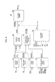
- FIG. 1 is a block diagram illustrating a semiconductor memory device, in accordance with an embodiment of the present invention.
- FIG. 2 is a circuit diagram illustrating a high frequency signal control unit shown in FIG. 1 .
- FIGS. 3A and 3B are timing diagrams illustrating examples of an operation of the high frequency signal control unit shown in FIG. 2 .
- FIG. 4A is a circuit diagram of a pulse width control unit shown in FIG. 1 in accordance with a first embodiment of the present invention
- FIG. 4B is an operation timing diagram of a pulse width control unit shown in FIG. 1 in accordance with the first embodiment of the present invention.
- FIG. 5A is a circuit diagram of a pulse width control unit shown in FIG. 1 in accordance with a second embodiment of the present invention.
- FIG. 5B is an operation timing diagram of a pulse width control unit shown in FIG. 1 in accordance with the second embodiment of the present invention.
- FIG. 6 is a block diagram illustrating a refresh operation control unit shown in FIG. 1 .
- FIG. 7 is a circuit diagram illustrating a redundancy refresh controller shown in FIG. 6 .
- FIGS. 8A and 8B are timing diagrams illustrating examples of an operation of the redundancy refresh controller shown in FIG. 7 .
- FIG. 9 is a circuit diagram illustrating a final refresh generator shown in FIG. 6 .
- FIGS. 10A and 10B are timing diagrams illustrating examples of an operation of the final refresh generator shown in FIG. 9 .
- FIG. 11 is a circuit diagram illustrating an internal second refresh controller shown in FIG. 6 .
- FIGS. 12A and 12B are timing diagrams illustrating examples of an operation of the internal second refresh controller shown in FIG. 11 .
- spatially relative terms such as “under,” “below,” “lower,” “above,” “upper” and the like, may be used herein for ease of description to describe one element or feature's relationship to another element(s) or feature(s) as illustrated in the figures. It will be understood that the spatially relative terms are intended to encompass different orientations of the device in manufacturing, use or operation in addition to the orientation depicted in the figures. For example, if the device in the figures is turned over, elements described as “below” or “under” other elements or features would then be “above” the other elements or features. The device may be otherwise oriented (rotated 90 degrees or at other orientations) and the spatially relative descriptors used herein interpreted accordingly.
- FIG. 1 is a block diagram illustrating a semiconductor memory device in accordance with an embodiment of the present invention.
- the semiconductor memory device may include a high frequency signal control unit 110 , a pulse width control unit 120 , a refresh operation control unit 130 , and a memory cell array 140 .
- the high frequency signal control unit 110 may receive an external command address signal CA and remove noise signals mixed with noise or glitch signals that are generated abnormally from the command address signal CA. In other words, the high frequency signal control unit 110 may remove noise signals or glitch signals that do not have a normal pulse width but have a very small pulse width from the command address signal CA and output a first command address signal CA 1 that is substantially of noise or glitch signals.
- the pulse width control unit 120 may receive the first command address signal CA 1 from the high frequency signal control unit 110 . If the pulse width of the first command address signal CA 1 is narrower than a predetermined pulse width, the pulse width control unit 120 may output the first command address signal CA 1 as it is as the second command address signal CA 2 . If the pulse width of the first command address signal CA 1 is wider than the predetermined pulse width, the pulse width control unit 120 may perform a control to reduce the wide pulse width of the first command address signal CA 1 to the predetermined pulse width and output it as command address signal CA 2 .
- the pulse width control unit 120 is a circuit tuned to maintain the pulse width of approximately 500 ps
- signals having a pulse width of approximately 1 ns may be reduced into signals of approximately 500 ps, while signals having a pulse width of approximately 300 ps may be controlled to be outputted as they are.
- the refresh operation control unit 130 may receive the second command address signal CA 2 from the pulse width control unit 120 , and generate a row address ROW ⁇ n> for performing an internal refresh operation.
- the refresh operation control unit 130 may include an internal circuit for controlling a redundancy refresh operation, a smart refresh operation, and a second refresh operation.
- the memory cell array 140 may receive the row address ROW ⁇ n> and enable a word line corresponding to the row address ROW ⁇ n>.
- FIG. 2 is a circuit diagram illustrating a configuration example of the high frequency signal control unit 110 shown in FIG. 1 .
- the high frequency signal control unit 110 may include a plurality of inverters and a plurality of NAND gates. Specifically, the high frequency signal control unit 110 includes inverters INV 1 , INV 2 , INV 3 , INV 4 , INV 5 , INV 6 , INV 7 and INV 8 and NAND gates NAND 1 and NAND 2 .
- the first NAND gate NAND 1 may perform a logic operation on the external command address signal CA and a first delay signal DLY 1 , which is a signal obtained by delaying the external command address signal CA through the first to fourth inverters INV 1 , INV 2 , INV 3 and INV 4 , and output an intermediate signal A.
- the second NAND gate NAND 2 may perform a logic operation on the intermediate signal A, received from the first NAND gate NAND 1 , and a second delay signal DLY 2 which is obtained by delaying the intermediate signal A through the fifth to eighth inverters INV 5 , INV 6 , INV 7 and INV 8 , and output the first command address signal CA 1 .
- the operation of the high frequency signal control unit 110 will be further described by referring to FIGS. 3A and 3B .
- FIGS. 3A and 3B are timing diagrams illustrating examples of the operation of the high frequency signal control unit 110 shown in FIG. 2 .
- FIG. 3A is a timing diagram illustrating the operation of the high frequency signal control unit 110 when the inputted external command address signal CA is not a normal signal but a noise signal or a glitch signal.
- the inputted external command address signal CA is not a signal having a normal pulse width but a signal having a very narrow pulse width, e.g., approximately 10 ps or less, and is therefore a noise signal or a glitch signal.
- the first NAND gate NAND 1 of FIG. 2 may perform a logic operation on the external command address signal CA and the first delay signal DLY 1 , which is obtained by delaying the external command address signal CA and output the intermediate signal A having a high logic value.
- the second delay signal DLY 2 may be also a signal having a high logic value.
- the first command address signal CA 1 outputted from the second NAND gate NAND 2 may be outputted in a logic low level.
- FIG. 3B is a timing diagram illustrating the operation of the high frequency signal control unit 110 when the inputted external command address signal CA is a signal having a normal pulse width.
- the first NAND gate NAND 1 of FIG. 2 may perform a logic operation on the external command address signal CA having a normal pulse width and the first delay signal DLY 1 , which is a signal obtained by delaying the external command address signal CA and output the intermediate signal A.
- the external command address signal CA is a signal having a normal pulse width
- the intermediate signal A having a predetermined pulse width may be generated.
- the second NAND gate NAND 2 may perform a logic operation on the intermediate signal A and the second delay signal DLY 2 , which is a signal obtained by delaying the intermediate signal A, and output the first command address signal CA 1 having the same pulse width as the external command address signal CA.
- the high frequency signal control unit 110 may decide that the external command address signal CA is not a normal signal but a noise signal or a glitch signal and remove the noise signal or the glitch signal from the inputted external command address signal CA.
- the high frequency signal control unit 110 may output the external command address signal CA while maintaining the pulse width of the external command address signal CA.
- FIGS. 4A and 4B are a circuit diagram and an operation timing diagram of the pulse width control unit 120 shown in FIG. 1 in accordance with a first embodiment of the present invention, respectively.
- the pulse width control unit 120 may include a ninth inverter INV 9 , a delayer 410 , and a NOR gate NOR 1 as a signal combiner.
- the ninth inverter INV 9 may invert the first command address signal CA 1 and output a first command address bar signal CA 1 B.
- the delayer 410 may delay the first command address bar signal CA 1 B by a predetermined duration and output a delay signal DLY_CA 1 B.
- the NOR gate NOR 1 may perform a logic operation on the first command address bar signal CA 1 B and the delay signal DLY_CA 1 B and output the second command address signal CA 2 .
- the operation of the pulse width control unit 120 is described now by referring to FIG. 4B .
- the first command address signal CA 1 may be inverted and as a result, the first command address bar signal CA 1 B may be generated.
- the first command address bar signal CA 1 B may be delayed by a predetermined duration and as a result, the delay signal DLY_CA 1 B may be generated.
- the delay signal DLY_CA 1 B and the first command address bar signal CA 1 B may be adjusted in the NOR gate NOR 1 to have a predetermined pulse width (e.g., approximately 500 ps) or the delay signal DLY_CA 1 B and the first command address bar signal CA 1 B may be outputted while maintaining the pulse width of the inputted first command address signal CA 1 .
- the predetermined pulse width may be determined in the delayer 410 .
- the predetermined pulse width may be determined according to the internal operation speed of a circuit. Generally, when the pulse width is approximately 500 ps, it signifies a state that there is no problem in the internal operation margin and the pulse width of approximately 500 ps may be set up. The pulse width does not have to be approximately 500 ps necessarily. The pulse width may be set up differently in an inverter (not shown) of the delayer 410 according to the characteristics of an internal circuit.
- the pulse width control unit 120 may operate in a plurality of cases according to the pulse width of the first command address signal CA 1 .
- the pulse width control unit 120 may output the second command address signal CA 2 while maintaining the pulse width of approximately 300 ps.
- the pulse width of approximately 300 ps is smaller than the predetermined pulse width PW, which is approximately 500 ps. Therefore the first command address signal CA 1 may be regarded as a glitch signal or a noise signal, but since glitch signals or noise signals have been already removed by the high frequency signal control unit 110 , the first command address signal CA 1 having the pulse width of approximately 300 ps may be considered as a normal signal. Therefore, the first command address signal CA 1 may be outputted while maintaining the pulse width of the first command address signal CA 1 .
- the pulse width of the first command address signal CA 1 much wider than the predetermined pulse width PW, which is approximately 500 ps.
- PW the pulse width of the predetermined pulse width
- FIGS. 5A and 5B are a circuit diagram and an operation timing diagram of the pulse width control unit 120 shown in FIG. 1 in accordance with a second embodiment of the present invention, respectively.
- the pulse width control unit 120 may include a delayer 510 and an AND gate AND 1 as a signal combiner.
- the delayer 510 may delay the first command address signal CA 1 by a predetermined section and generate a delay signal DLY_CA 1 .
- the AND gate AND 1 may perform a logic operation on the first command address signal CA 1 and the delay signal DL_CA 1 and output the second command address signal CA 2 .
- the AND gate AND 1 may perform a logic operation on the first command address signal CA 1 and a delay signal DLY_CA 1 which is a signal obtained by delaying the first command address signal CA 1 by a predetermined duration in order to adjust the first command address signal CA 1 to have the predetermined pulse width (e.g., approximately 500 ps), or the inputted first command address signal CA 1 may be outputted while maintaining its pulse width as it is.
- the predetermined pulse width may be determined in the delayer 510 .
- the pulse width control unit 120 may operate in a plurality of cases according to the pulse width of the first command address signal CAL Since the operation cases of the pulse width control unit 120 are described above by referring to FIG. 4B , further description is not provided herein.
- FIG. 6 is a block diagram illustrating a refresh operation control unit 130 shown in FIG. 1 .
- the refresh operation control unit 130 may include a command decoder 610 , a smart refresh controller 620 , a refresh counter 630 , a redundancy refresh controller 640 , an internal second refresh controller 650 , an internal second refresh command generator 660 , a final refresh generator 670 , and a row address controller 680 .
- the command decoder 610 may generate a plurality of command signals AFACT and ACT in response to the second command address signal CA 2 .
- the command signals AFACT and ACT may include an auto-refresh command AFACT, an active command ACT and the like.
- the second command address signal CA 2 may be a signal whose pulse width is adjusted by the pulse width control unit 120 .
- the smart refresh controller 620 may generate a smart refresh enable signal SRREFENB for performing a smart refresh operation with respect to a target row address (not shown) in response to a final refresh command REF.
- the target row address (not shown) may be an n ⁇ 1/n+1 row address with respect to a target row address ROW ⁇ n>.
- the final refresh command REF may be generated by the final refresh generator 670 , which will be described later on.
- the refresh counter 630 may generate a redundancy refresh enable signal REDREFEN in response to the auto-refresh command AFACT and the smart refresh enable signal SRREFENB. For example, the refresh counter 630 may count the auto-refresh command AFACT and generate the redundancy refresh enable signal REDREFEN for refreshing not a normal cell but a redundancy cell at every eighth auto-refresh command AFACT.
- the redundancy refresh controller 640 may generate a redundancy refresh command PTXREF in response to the auto-refresh command AFACT, a redundancy refresh control signal TM_REDON, the redundancy refresh enable signal REDREFEN, and a reset signal RSTB.
- a redundancy cell region may be region for repairing a failure cell, when a failure cell occurs in a normal cell region.
- the internal second refresh controller 650 may generate a double refresh enable signal HDREFEN in response to the smart refresh enable signal SRREFENB, the auto refresh command AFACT, a second refresh command AFACT 2 ND, a double refresh signal DREF, and a section selection signal HRMSELB.
- the double refresh enable signal HDREFEN is a signal for doubling i.e., increasing by two times the number of refresh operations in response to one auto-refresh command AFACT inputted once, and the double refresh enable signal HDREFEN may be applied to all refresh operation.
- the double refresh enable signal HDREFEN may also be applied not to all the refresh operations but to some refresh operations of a predetermined section.
- the double refresh enable signal HDREFEN may be controlled based on whether the section selection signal HRMSELB is enabled or not. Also, when the internal second refresh controller 650 generates the double refresh enable signal HDREFEN which performs a control to internally perform a refresh operation twice when the auto-refresh command AFACT is inputted once, an operation for resetting the refresh operation so that the internal refresh operation is not performed three times is required. Such reset operation may be controlled based on the second refresh command AFACT 2 ND.
- the double refresh signal DREF and the section selection signal HRMSELB may be generated in an auto-refresh operation number control circuit (not shown).
- the internal second refresh command generator 660 may generate the second refresh command AFACT 2 ND in response to the double refresh enable signal HDREFEN, which is generated by the internal second refresh controller 650 .
- the second refresh command AFACT 2 ND may be a command for performing a refresh operation two times in a predetermined section, although the auto-refresh command AFACT is inputted once.
- the predetermined section is a refresh row cycle time tRFC which may be an active-precharge time tRP that has to be secured minimally.
- the final refresh generator 670 may generate the final refresh command REF in response to the auto-refresh command AFACT, the second refresh command AFACT 2 ND, a wafer burn-in signal WBI, a test mode signal TM, a self-refresh command PSRF, an idle signal IDLE, and the reset signal RSTB.
- the final refresh generator 670 may generate the final refresh command REF for refreshing the memory cell array 140 of FIG. 1 , when any one command among the self-refresh command PSRF, the auto-auto-refresh command AFACT, and the second refresh command AFACT 2 ND that is generated based on the auto-refresh command AFACT.
- a refresh command may be inputted as a test mode signal TM.
- the wafer burn-in signal WBI and the test mode signal TM may be the commands inputted for the purpose.
- the idle signal IDLE is a signal that is generated when the refresh rove cycle time tRFC passes after the external command address signal CA is inputted.
- the idle signal IDLE performs a control to make other normal operations performed after a refresh operation ends.
- the row address controller 580 may enable the row address ROW ⁇ n> in response to the smart refresh enable signal SRREFENB, the redundancy refresh command PTXREF, the active command ACT, and the final refresh command REF.
- the row address controller 680 may perform a control to enable the n ⁇ 1/n+1 row addresses with respect to the target row address ROW ⁇ n>, when a smart refresh operation is performed.
- the row address controller 680 may perform a control to enable the row address ROW ⁇ n> that corresponds to the redundancy cell region in response to the redundancy refresh command PTXREF.
- FIG. 7 is a circuit diagram illustrating a configuration example of the redundancy refresh controller 640 shown in FIG. 6 .
- the redundancy refresh controller 640 may include a set signal generator 710 and a latch 720 .
- the set signal generator 710 may be formed of a NAND gate NAND 3 .
- the set signal generator 710 may perform a logic operation on the auto-refresh command AFACT, the redundancy refresh control signal TM_REDON and the redundancy refresh enable signal REDREFEN and generate a redundancy set signal REDSET.
- the latch 720 may include an SR latch that is formed of two NAND gates NAND 4 and NAND 5 .
- the latch 720 may receive the redundancy set signal REDSET as a set signal, receive the redundancy refresh enable signal REDREFEN or the reset signal RSTB as a reset signal, and generate the redundancy refresh command PTXREF.
- the redundancy refresh command PTXREF may be enabled in response to the redundancy set signal REDSET, and may be disabled in response to the redundancy refresh enable signal REDREFEN or the reset signal RSTB.
- redundancy refresh controller 640 is described with reference to FIGS. 8A and 8B .
- FIGS. 8A and 8B are timing diagrams illustrating examples of an operation of the redundancy refresh controller 640 shown in FIG. 7 .
- FIG. 8A is a timing diagram illustrating the operation of the redundancy refresh controller 640 in accordance with a comparative example of the present invention.
- the auto-refresh command AFACT shown in FIG. 8A may be generated based on the external command address signal CA that does not go through the pulse width control unit 120 . Therefore, the auto-refresh command AFACT may have a wider pulse width than the predetermined pulse width (e.g., approximately 500 ps).
- the redundancy refresh enable signal REDREFEN is a signal for performing a control to refresh the redundancy cell region in the eighth refresh operation during an auto-refresh operation.
- the redundancy refresh enable signal REDREFEN may be enabled at a timing when the seventh refresh operation ends.
- an N th auto-refresh command AFACT may be generated for performing the seventh refresh operation, which is a normal refresh operation
- an (N+1) th auto-refresh command AFACT may be generated for performing the eighth refresh operation, which is a redundancy refresh operation.
- the redundancy set signal REDSET may be enabled in response to the enabling of the redundancy refresh enable signal REDREFEN, and thereby the redundancy refresh command PTXREF may be generated.
- the redundancy refresh enable signal REDREFEN may be generated before an enabling section of the N th auto-refresh command AFACT ends. Since the refresh operation ends before the enabling section of the auto-refresh command AFACT ends, there may be a section where the pulse widths overlap. Therefore, the redundancy refresh command PTXREF is enabled not in an enabling section of the (N+1) th auto-refresh command AFACT but in an enabling section of the N th auto-refresh command AFACT, and the refresh operation is performed not in the normal cell region but in the redundancy cell region during the seventh refresh operation, malfunction may be caused.
- FIG. 8B is a timing diagram illustrating the operation of the redundancy refresh controller 640 in accordance with an embodiment of the present invention.
- the external command address signal CA having a wider pulse width than the predetermined pulse width e.g., approximately 500 ps) may be adjusted to have the predetermined pulse width by the pulse width control unit 120 , and outputted as the second command address signal CA 2 (not shown). Since the auto-refresh command AFACT is generated based on the second command address signal CA 2 having the predetermined pulse width, the outputted auto-refresh command AFACT may have the predetermined pulse width.
- the redundancy refresh enable signal REDREFEN may be enabled at a moment when the seventh normal refresh operation ends, which is after the N th enabling section of the auto-refresh command AFACT ends. Therefore, the redundancy refresh command PTXREF may be enabled at a moment when the auto-refresh command AFACT is enabled (N+1) times, which is the normal eighth refresh operation section. Thus, it is possible to normally perform a refresh operation on the redundancy cell region.
- FIG. 9 is a circuit diagram illustrating an example of the final refresh generator 670 shown in FIG. 6 .
- the final refresh generator 670 may include a set signal generator 910 and a latch 920 .
- the set signal generator 910 may include a plurality of NAND gates NAND 6 and NAND 8 , a plurality of inverters INV 10 and INV 11 , and a NOR gate NOR 2 .
- the sixth NAND gate NAND 6 may perform a logic operation on the test mode signal TM and the wafer burn-in signal WBI and output an output signal.
- the NOR gate NOR 2 may perform a logic operation on the auto-refresh command AFACT, the second refresh command AFACT 2 ND, and a signal that is obtained by inverting the output signal outputted from the sixth NAND gate NAND 6 by the 10 th inverter INV 10 , and output the logic operation result.
- the NOR gate NOR 2 may be able to output a signal having a logic low level, when at least one signal among the auto-refresh command AFACT, the second refresh command AFACT 2 ND, and the signal that is obtained by inverting the output signal outputted from the sixth NAND gate NAND 6 by the 10 th inverter INV 10 , is enabled.
- the eighth NAND gate NAND 8 may perform a logic operation on a signal obtained by inverting a signal outputted from the NOR gate NOR 2 by the 11 th inverter INV 11 and a delayed/inverted auto-refresh command AFACTDB, and output a net signal NET.
- the delayed/inverted auto-refresh command AFACTDB may be a signal maintaining a predetermined pulse width regardless of the pulse width because the delayed/inverted auto-refresh command AFACTDB is generated through self-generation (not shown) based on the pulse of the auto-refresh command AFACT.
- the set signal generator 910 may generate the net signal NET in response to the auto-refresh command AFACT or the second refresh command AFACT 2 ND.
- the latch 920 may include an SR latch that is formed of a plurality of NAND gates NAND 9 and NAND 10 .
- the latch 920 may receive a self-refresh command PSRF or the net signal NET as a set signal, receive the idle signal IDLE or the reset signal RSTB as a reset signal, and generate the final refresh command REF.
- the final refresh command REF is enabled in response to one signal among the self-refresh command PSRF, the auto-refresh command AFACT, and the second refresh command AFACT 2 ND, and disabled in response to the idle signal IDLE or the reset signal RSTB.
- FIGS. 10A and 10B are timing diagrams illustrating examples of the operation of the final refresh generator 670 shown in FIG. 9 .
- FIG. 10A is a timing diagram illustrating the operation of the final refresh generator 670 in accordance with a comparative example of the present invention.
- the auto-refresh command AFACT may be generated based on the external command address signal CA that does not go through the pulse width control unit 120 . Therefore, the auto-refresh command AFACT may have a much wider pulse width than the predetermined pulse width (e.g., approximately 500 ps).
- the second refresh command AFACT 2 ND is a command for performing a refresh operation two times within a refresh row cycle time tRFC in order to complement the refresh performance of a memory cell, although the auto-refresh command AFACT is inputted just once.
- the second refresh command AFACT 2 ND may be generated in the internal second refresh command generator 660 .
- the delayed/inverted auto-refresh command AFACTDB may be obtained by delaying the auto-refresh command AFACT by a predetermined duration and then inverting the delayed auto-refresh command AFACT.
- the set signal generator 910 may generate the net signal NET by logically combining the signals.
- a logic operation may be performed on the net signal NET and the delayed/inverted auto-refresh command AFACTDB and then a logic operation result signal may be outputted, when the auto-refresh command AFACT or the second refresh command AFACT 2 ND is enabled.
- the pulse width of the auto-refresh command AFACT is as wide as to include the pulse width of the second refresh command AFACT 2 ND
- the pulse width of the delayed/inverted auto-refresh command AFACTDB is wide as well. Therefore, since the net signal NET may not be additionally enabled although the second refresh command AFACT 2 ND is enabled, the final refresh command REF is also enabled just once. Thus, the final refresh command REF may not be normally generated, which may lead to malfunction.
- FIG. 10B is a timing diagram illustrating the operation of the final refresh generator 670 in accordance with an embodiment of the present invention.
- the external command address signal CA having a wider pulse width than the predetermined pulse width e.g., approximately 500 ps) may be adjusted to have the predetermined pulse width by the pulse width control unit 120 and outputted as the second command address signal CA 2 . Since the auto-refresh command AFACT is generated based on the second command address signal CA 2 which has the predetermined pulse width, the auto-refresh command AFACT may also have the predetermined pulse width.
- the delayed/inverted auto-refresh command AFACTDB may be also generated to have the same pulse width as the auto-refresh command AFACT. Therefore, the net signal NET is enabled when the auto-refresh command AFACT is enabled and when the second refresh command AFACT 2 ND is enabled, and thereby the final refresh command REF may be normally generated. In this way, it is possible to perform a normal refresh operation.
- FIG. 11 is a circuit diagram illustrating an internal second refresh controller 650 shown in FIG. 6 .
- the internal second refresh controller 650 may include a set signal generator 1100 , a reset signal generator 1200 , and a latch 1300 .
- the set signal generator 1100 may include a plurality of NAND gates NAND 11 , NAND 12 and NAND 13 , and an inverter INV 12 .
- the NAND gates NAND 11 , NAND 12 and NAND 13 and the inverter INV 12 may generate a net signal NET 2 by performing a logic operation on the auto-refresh command AFACT, the double refresh signal DREF, the section selection signal HRMSELB, and the smart refresh enable signal SRREFENB.
- the reset signal generator 1200 may be formed of a NOR gate NOR 3 .
- the reset signal generator 1200 may perform a logic operation on an output signal outputted from the 12 th NAND gate NAND 12 and the second refresh command AFACT 2 ND and output a logic operation result.
- the latch 1300 may include an SR latch that is formed of two NAND gates NAND 14 and NAND 15 .
- the latch 1300 may receive the net signal NET 2 as a set signal, receive a signal outputted from the reset signal generator 1200 as a reset signal, and generate the double refresh enable signal HDREFEN.
- the double refresh enable signal HDREFEN may be enabled in response to the net signal NET 2 , and may be disabled in response to the signal outputted from the reset signal generator 1200 .
- the smart refresh enable signal SRREFENB is a signal that is enabled during a smart refresh operation.
- the smart refresh enable signal SRREFENB may stay in a logic low level in the other refresh sections that are not a smart refresh operation section.
- the double refresh signal DREF is a signal for increasing the number of internal refresh operations into two times with respect to one auto-refresh command AFACT which is inputted once.
- the double refresh signal DREF may be an enabling signal that controls the operation of the internal second refresh controller 650 .
- the section selection signal HRMSELB may be a signal for increasing the number of internal refresh operations into two times with respect to one auto-refresh command AFACT which is inputted once within a predetermined section.
- the section selection signal HRMSELB does not make all the internal refresh operations be performed two times with respect to one auto-refresh command AFACT.
- the double refresh signal DREF may be in a logic high level
- the smart refresh enable signal SRREFENB may be in a logic low level
- the section selection signal HRMSELB may be in a logic high level or in a logic low level.
- the auto-refresh command AFACT may be inputted while maintaining a predetermined pulse width.
- a signal outputted from the 11 th NAND gate NAND 11 may be in a logic high level
- a signal outputted from the 12 th NAND gate NAND 12 may be in a logic low level
- the 13 th NAND gate NAND 13 may output the net signal NET 2 in a logic low level in a section where the auto-refresh command AFACT is inputted.
- the enabling of the net signal NET 2 may be controlled based on the auto-refresh command AFACT.
- the third NOR gate NOR 3 may output a signal having a logic low level as a reset signal in response to the logic-low-level signal outputted from the 12 th NAND gate NAND 12 and the second refresh command AFACT 2 ND that is enabled to a logic high level.
- the enabling of the reset signal may be controlled based on the second refresh command AFACT 2 ND.
- the double refresh enable signal HDREFEN may be enabled in response to the auto-refresh command AFACT, and may be disabled in response to the second refresh command AFACT 2 ND.
- FIGS. 12A and 12B are timing diagrams illustrating examples of an operation of the internal second refresh controller 650 shown in FIG. 11 .
- FIG. 12A is a timing diagram illustrating the operation of the internal second refresh controller 650 in accordance with a comparative example of the present invention.
- the auto-refresh command AFACT may be a signal generated based on the external command address signal CA that does not go through the pulse width control unit 120 . Therefore, the auto-refresh command AFACT may have a much wider pulse width than the predetermined pulse width (e.g. approximately 500 ps).
- the double refresh enable signal HDREFEN which is enabled according to the enabling of the auto-refresh command AFACT and disabled according to the enabling of the second refresh command AFACT 2 ND, may not be disabled although the second refresh command AFACT 2 ND is enabled and continue to be enabled. Therefore, when the internal refresh operation has to be performed two times during one auto-refresh operation, the internal refresh operation may be continuously performed more than three times or four times, which is malfunction.
- FIG. 12B is a timing diagram illustrating the operation of the internal second refresh controller 650 in accordance with an embodiment of the present invention.
- the external command address signal CA having a wider pulse width than the predetermined pulse width may be adjusted to have the predetermined pulse width by the pulse width control unit 120 and outputted as the second command address signal CA 2 (not shown). Since the auto-refresh command AFACT is generated based on the second command address signal CA 2 which has the predetermined pulse width, the auto-refresh command AFACT may also have the predetermined pulse width.
- the double refresh enable signal HDREFEN may be enabled in response to the auto-refresh command AFACT, and may be disabled in response to the second refresh command AFACT 2 ND, and thereby it is possible to perform an internal operation normally.
- the semiconductor memory device in accordance with the embodiments of the present invention may be able to adjust the pulse width into the predetermined pulse width to prevent malfunction internally. Also, when the external command address signal CA is inputted as a normal signal, the semiconductor memory device in accordance with the embodiments of the present invention may be able to output the signal as it is without adjustment. Therefore, the semiconductor memory device in accordance with the embodiments of the present invention may be able to perform an internal operation normally even though a signal having a wide pulse width is inputted from the exterior.
- a semiconductor memory device may perform a refresh operation normally by controlling the pulse width of an external command address to be uniform, when the semiconductor memory device performs a refresh operation based on the external command address under the condition of a low clock cycle tCK.
Landscapes
- Engineering & Computer Science (AREA)
- Microelectronics & Electronic Packaging (AREA)
- Computer Hardware Design (AREA)
- Dram (AREA)
Abstract
Description
Claims (17)
Applications Claiming Priority (2)
| Application Number | Priority Date | Filing Date | Title |
|---|---|---|---|
| KR10-2016-0080555 | 2016-06-28 | ||
| KR1020160080555A KR102535662B1 (en) | 2016-06-28 | 2016-06-28 | Semiconductor memory device and operating method thereof |
Publications (2)
| Publication Number | Publication Date |
|---|---|
| US20170372770A1 US20170372770A1 (en) | 2017-12-28 |
| US10037793B2 true US10037793B2 (en) | 2018-07-31 |
Family
ID=60677461
Family Applications (1)
| Application Number | Title | Priority Date | Filing Date |
|---|---|---|---|
| US15/398,884 Active US10037793B2 (en) | 2016-06-28 | 2017-01-05 | Semiconductor memory device and method for operating the same |
Country Status (2)
| Country | Link |
|---|---|
| US (1) | US10037793B2 (en) |
| KR (1) | KR102535662B1 (en) |
Citations (3)
| Publication number | Priority date | Publication date | Assignee | Title |
|---|---|---|---|---|
| US4433331A (en) * | 1981-12-14 | 1984-02-21 | Bell Telephone Laboratories, Incorporated | Programmable logic array interconnection matrix |
| US6771558B2 (en) | 2001-12-21 | 2004-08-03 | Hynix Semiconductor Inc. | Semiconductor memory device |
| US20070159905A1 (en) * | 2006-01-09 | 2007-07-12 | Hynix Semiconductor Inc. | Circuit for controlling pulse width of auto-refresh signal and circuit for generating internal row address for auto refresh |
Family Cites Families (1)
| Publication number | Priority date | Publication date | Assignee | Title |
|---|---|---|---|---|
| JP3409059B2 (en) * | 2000-07-26 | 2003-05-19 | Necエレクトロニクス株式会社 | Semiconductor storage device |
-
2016
- 2016-06-28 KR KR1020160080555A patent/KR102535662B1/en active Active
-
2017
- 2017-01-05 US US15/398,884 patent/US10037793B2/en active Active
Patent Citations (4)
| Publication number | Priority date | Publication date | Assignee | Title |
|---|---|---|---|---|
| US4433331A (en) * | 1981-12-14 | 1984-02-21 | Bell Telephone Laboratories, Incorporated | Programmable logic array interconnection matrix |
| US6771558B2 (en) | 2001-12-21 | 2004-08-03 | Hynix Semiconductor Inc. | Semiconductor memory device |
| US20070159905A1 (en) * | 2006-01-09 | 2007-07-12 | Hynix Semiconductor Inc. | Circuit for controlling pulse width of auto-refresh signal and circuit for generating internal row address for auto refresh |
| US7852134B2 (en) * | 2006-01-09 | 2010-12-14 | Hynix Semiconductor Inc. | Circuit for controlling pulse width of auto-refresh signal and circuit for generating internal row address for auto refresh |
Also Published As
| Publication number | Publication date |
|---|---|
| KR20180002087A (en) | 2018-01-08 |
| US20170372770A1 (en) | 2017-12-28 |
| KR102535662B1 (en) | 2023-05-25 |
Similar Documents
| Publication | Publication Date | Title |
|---|---|---|
| US10930335B2 (en) | Apparatuses and methods for selective row refreshes | |
| US9570119B2 (en) | Information processing system including semiconductor device having self-refresh mode | |
| US7180807B2 (en) | Semiconductor memory device having a delay circuit | |
| US8724416B2 (en) | Information processing system including semiconductor device having self-refresh mode | |
| US9520169B2 (en) | Semiconductor device | |
| US8284614B2 (en) | Refresh control circuit and method for semiconductor memory device | |
| US9455019B2 (en) | Semiconductor device having CAL latency function | |
| US8769194B2 (en) | Information processing system including semiconductor device having self-refresh mode | |
| US8923082B2 (en) | Semiconductor device on which wafer-level burn-in test is performed and manufacturing method thereof | |
| US20150213859A1 (en) | Burst length control circuit | |
| US9019784B2 (en) | Data training device | |
| US8811105B2 (en) | Information processing system including semiconductor device having self-refresh mode | |
| US7710804B2 (en) | Auto precharge circuit sharing a write auto precharge signal generating unit | |
| US7835180B2 (en) | Semiconductor memory device | |
| US7167948B2 (en) | Semiconductor memory device | |
| US10181343B2 (en) | Semiconductor device including a clock adjustment circuit | |
| US11257561B2 (en) | Memory device and test method thereof | |
| US10037793B2 (en) | Semiconductor memory device and method for operating the same | |
| US10957378B1 (en) | Control circuit and control method thereof for pseudo static random access memory | |
| US8488404B2 (en) | Counter control signal generator and refresh circuit | |
| US7751271B2 (en) | Semiconductor memory device | |
| KR20050067449A (en) | Row active time control circuit in semiconductor memory device |
Legal Events
| Date | Code | Title | Description |
|---|---|---|---|
| AS | Assignment |
Owner name: SK HYNIX INC., KOREA, REPUBLIC OF Free format text: ASSIGNMENT OF ASSIGNORS INTEREST;ASSIGNORS:HYUN, SANG-AH;HWANG, JEONG-TAE;REEL/FRAME:041257/0571 Effective date: 20161227 |
|
| STCF | Information on status: patent grant |
Free format text: PATENTED CASE |
|
| MAFP | Maintenance fee payment |
Free format text: PAYMENT OF MAINTENANCE FEE, 4TH YEAR, LARGE ENTITY (ORIGINAL EVENT CODE: M1551); ENTITY STATUS OF PATENT OWNER: LARGE ENTITY Year of fee payment: 4 |
|
| AS | Assignment |
Owner name: MIMIRIP LLC, TEXAS Free format text: ASSIGNMENT OF ASSIGNORS INTEREST;ASSIGNOR:SK HYNIX INC.;REEL/FRAME:067335/0246 Effective date: 20240311 Owner name: MIMIRIP LLC, TEXAS Free format text: ASSIGNMENT OF ASSIGNOR'S INTEREST;ASSIGNOR:SK HYNIX INC.;REEL/FRAME:067335/0246 Effective date: 20240311 |
|
| MAFP | Maintenance fee payment |
Free format text: PAYMENT OF MAINTENANCE FEE, 8TH YEAR, LARGE ENTITY (ORIGINAL EVENT CODE: M1552); ENTITY STATUS OF PATENT OWNER: LARGE ENTITY Year of fee payment: 8 |