US10026644B2 - Fabricating method of non-volatile memory device - Google Patents
Fabricating method of non-volatile memory device Download PDFInfo
- Publication number
- US10026644B2 US10026644B2 US14/704,986 US201514704986A US10026644B2 US 10026644 B2 US10026644 B2 US 10026644B2 US 201514704986 A US201514704986 A US 201514704986A US 10026644 B2 US10026644 B2 US 10026644B2
- Authority
- US
- United States
- Prior art keywords
- word lines
- bit lines
- lines
- line
- substrate
- Prior art date
- Legal status (The legal status is an assumption and is not a legal conclusion. Google has not performed a legal analysis and makes no representation as to the accuracy of the status listed.)
- Active, expires
Links
Images


Classifications
-
- H01L21/768—
-
- H—ELECTRICITY
- H10—SEMICONDUCTOR DEVICES; ELECTRIC SOLID-STATE DEVICES NOT OTHERWISE PROVIDED FOR
- H10B—ELECTRONIC MEMORY DEVICES
- H10B41/00—Electrically erasable-and-programmable ROM [EEPROM] devices comprising floating gates
- H10B41/20—Electrically erasable-and-programmable ROM [EEPROM] devices comprising floating gates characterised by three-dimensional [3D] arrangements, e.g. with cells on different height levels
-
- G—PHYSICS
- G11—INFORMATION STORAGE
- G11C—STATIC STORES
- G11C16/00—Erasable programmable read-only memories
- G11C16/02—Erasable programmable read-only memories electrically programmable
- G11C16/04—Erasable programmable read-only memories electrically programmable using variable threshold transistors, e.g. FAMOS
- G11C16/0408—Erasable programmable read-only memories electrically programmable using variable threshold transistors, e.g. FAMOS comprising cells containing floating gate transistors
-
- G—PHYSICS
- G11—INFORMATION STORAGE
- G11C—STATIC STORES
- G11C16/00—Erasable programmable read-only memories
- G11C16/02—Erasable programmable read-only memories electrically programmable
- G11C16/04—Erasable programmable read-only memories electrically programmable using variable threshold transistors, e.g. FAMOS
- G11C16/0483—Erasable programmable read-only memories electrically programmable using variable threshold transistors, e.g. FAMOS comprising cells having several storage transistors connected in series
-
- G—PHYSICS
- G11—INFORMATION STORAGE
- G11C—STATIC STORES
- G11C16/00—Erasable programmable read-only memories
- G11C16/02—Erasable programmable read-only memories electrically programmable
- G11C16/06—Auxiliary circuits, e.g. for writing into memory
- G11C16/10—Programming or data input circuits
- G11C16/14—Circuits for erasing electrically, e.g. erase voltage switching circuits
-
- G—PHYSICS
- G11—INFORMATION STORAGE
- G11C—STATIC STORES
- G11C16/00—Erasable programmable read-only memories
- G11C16/02—Erasable programmable read-only memories electrically programmable
- G11C16/06—Auxiliary circuits, e.g. for writing into memory
- G11C16/26—Sensing or reading circuits; Data output circuits
-
- H01L23/5222—
-
- H01L27/11524—
-
- H01L27/11551—
-
- H—ELECTRICITY
- H10—SEMICONDUCTOR DEVICES; ELECTRIC SOLID-STATE DEVICES NOT OTHERWISE PROVIDED FOR
- H10B—ELECTRONIC MEMORY DEVICES
- H10B41/00—Electrically erasable-and-programmable ROM [EEPROM] devices comprising floating gates
- H10B41/10—Electrically erasable-and-programmable ROM [EEPROM] devices comprising floating gates characterised by the top-view layout
-
- H—ELECTRICITY
- H10—SEMICONDUCTOR DEVICES; ELECTRIC SOLID-STATE DEVICES NOT OTHERWISE PROVIDED FOR
- H10B—ELECTRONIC MEMORY DEVICES
- H10B41/00—Electrically erasable-and-programmable ROM [EEPROM] devices comprising floating gates
- H10B41/30—Electrically erasable-and-programmable ROM [EEPROM] devices comprising floating gates characterised by the memory core region
- H10B41/35—Electrically erasable-and-programmable ROM [EEPROM] devices comprising floating gates characterised by the memory core region with a cell select transistor, e.g. NAND
-
- H—ELECTRICITY
- H10—SEMICONDUCTOR DEVICES; ELECTRIC SOLID-STATE DEVICES NOT OTHERWISE PROVIDED FOR
- H10D—INORGANIC ELECTRIC SEMICONDUCTOR DEVICES
- H10D30/00—Field-effect transistors [FET]
- H10D30/60—Insulated-gate field-effect transistors [IGFET]
- H10D30/68—Floating-gate IGFETs
-
- H—ELECTRICITY
- H10—SEMICONDUCTOR DEVICES; ELECTRIC SOLID-STATE DEVICES NOT OTHERWISE PROVIDED FOR
- H10D—INORGANIC ELECTRIC SEMICONDUCTOR DEVICES
- H10D30/00—Field-effect transistors [FET]
- H10D30/60—Insulated-gate field-effect transistors [IGFET]
- H10D30/68—Floating-gate IGFETs
- H10D30/681—Floating-gate IGFETs having only two programming levels
-
- H—ELECTRICITY
- H10—SEMICONDUCTOR DEVICES; ELECTRIC SOLID-STATE DEVICES NOT OTHERWISE PROVIDED FOR
- H10W—GENERIC PACKAGES, INTERCONNECTIONS, CONNECTORS OR OTHER CONSTRUCTIONAL DETAILS OF DEVICES COVERED BY CLASS H10
- H10W20/00—Interconnections in chips, wafers or substrates
- H10W20/01—Manufacture or treatment
-
- H—ELECTRICITY
- H10—SEMICONDUCTOR DEVICES; ELECTRIC SOLID-STATE DEVICES NOT OTHERWISE PROVIDED FOR
- H10W—GENERIC PACKAGES, INTERCONNECTIONS, CONNECTORS OR OTHER CONSTRUCTIONAL DETAILS OF DEVICES COVERED BY CLASS H10
- H10W20/00—Interconnections in chips, wafers or substrates
- H10W20/40—Interconnections external to wafers or substrates, e.g. back-end-of-line [BEOL] metallisations or vias connecting to gate electrodes
- H10W20/495—Capacitive arrangements or effects of, or between wiring layers
-
- G—PHYSICS
- G11—INFORMATION STORAGE
- G11C—STATIC STORES
- G11C16/00—Erasable programmable read-only memories
- G11C16/02—Erasable programmable read-only memories electrically programmable
- G11C16/06—Auxiliary circuits, e.g. for writing into memory
- G11C16/10—Programming or data input circuits
- G11C16/14—Circuits for erasing electrically, e.g. erase voltage switching circuits
- G11C16/16—Circuits for erasing electrically, e.g. erase voltage switching circuits for erasing blocks, e.g. arrays, words, groups
Definitions
- the present invention relates to a non-volatile memory device, and an operation method and a fabrication method thereof, and more particularly to a NAND flash memory having a zigzag body wiring, and an operation method and a fabrication method thereof.
- FIG. 1 there are the cross-sections of bit lines.
- the distance between neighboring bit lines is wider at the upper lines than at the lower lines.
- the number of bit lines per unit space is larger at the lower, but the parasitic capacitance which causes the bit line delay exists.
- SA-STI shallow trench isolation
- the self-align shallow trench isolation SA-STI which is an important invention for the device scaling of NAND flash, greatly enhances the parasitic capacitance between neighboring bit lines. Therefore, the bit line delay has become notable with the scaling.
- FIG. 2 there are the cross-sections of word lines.
- the distance between neighboring word lines is wider at the upper lines than at the lower lines.
- the number of word lines per unit space is larger at the lower, but the parasitic capacitance which causes the word line delay exists.
- the cell-to-cell space is shrunk as the memory cell is miniaturized. Accordingly, the parasitic capacitance between neighboring word lines is increased with the device scaling of NAND cells. Therefore, the word line delay has become notable with the scaling.
- the present invention provides a non-volatile memory device, which includes: a well, disposed in a substrate; a plurality of first word lines and a plurality of second word lines, disposed on the substrate, arranged periodically and extending in a first direction; a plurality of inter-poly dielectric films, disposed on the substrate and respectively beneath the plurality of first word lines and the plurality of second word lines; a plurality of floating gates, disposed between the well and the plurality of inter-poly dielectric films; and a plurality of tunnel oxide films, disposed between the well and the plurality of floating gates, wherein a first distance from the first word lines to the substrate is smaller than a second distance from the second word lines to the substrate.
- a third distance from a top of the first word lines to the substrate is smaller than or equal to a fourth distance from a bottom of the second word lines to the substrate.
- the plurality of inter-poly dielectric films include a plurality of first inter-poly dielectric films disposed on the substrate and respectively beneath the first word lines, and a plurality of second inter-poly dielectric films disposed on the substrate and respectively beneath the second word lines, wherein a thickness of the plurality of first inter-poly dielectric films is smaller than a thickness of the plurality of second inter-poly dielectric films.
- the plurality of floating gates include a plurality of first floating gates disposed on the substrate and respectively beneath the plurality of first word lines, and a plurality of second floating gates disposed on the substrate and respectively beneath the plurality of second word lines, wherein a thickness of the plurality of first floating gates is smaller than a thickness of the plurality of second floating gates.
- the non-volatile memory device further includes a plurality of bit lines disposed above the first word lines and the second word lines and extending along a second direction different from the first direction.
- the plurality of bit lines include a plurality of first bit lines and a plurality of second bit lines, and a fifth distance from the first bit lines to the substrate is smaller than a sixth distance from the second bit lines to the substrate.
- the present invention further provides a method for operating a non-volatile memory device having a substrate, a well, a plurality of first inter-poly dielectric films, a plurality of second inter-poly dielectric films, a plurality of first word lines and a plurality of second word lines disposed on the substrate and tunnel oxide films, wherein a first distance from the first word lines to the substrate being smaller than a second distance from the second word lines to the substrate.
- the method includes applying a first operating voltage to the first word lines, and applying a second operating voltage to the second word lines.
- the first operating voltage includes a first program voltage, a first erase voltage, a first pass voltage or a first read voltage
- the second operating voltage includes a second program voltage, a second erase voltage, a second pass voltage or a second read voltage
- the method further includes the following steps for programming the non-volatile memory device.
- the first program voltage is applied to a first word line
- the second program voltage is applied to a second word line.
- V PGM-A is the first program voltage applied to the first word line
- V PGM-B is the second program voltage applied to the second word line
- C rA is a first capacitance coupling ratio determined by a ratio of a capacitance of the first inter-poly dielectric films to a sum of capacitances of the first inter-poly dielectric films and the tunnel oxide films
- C rB is a second capacitance coupling ratio determined by a ratio of a capacitance of the second inter-poly dielectric films to a sum of capacitances of the second inter-poly dielectric films and the tunnel oxide films.
- the method further includes the following steps for erasing the non-volatile memory device.
- a well voltage is applied to the well
- the first erase voltage is applied to the first word lines
- the second erase voltage is applied to the second word lines.
- C rA is a first capacitance coupling ratio determined by a ratio of a capacitance of the first inter-poly dielectric films to a sum of capacitances of the first inter-poly dielectric films and the tunnel oxide films
- C rB is a second capacitance coupling ratio determined by a ratio of a capacitance of the second inter-poly dielectric films to a sum of capacitances of the second inter-poly dielectric films and the tunnel oxide films
- V well is the well voltage
- V CG-A is the first erase voltage applied to the first word lines
- V CG-B is the second erase voltage applied to the second word lines.
- the method further includes the following steps for reading the non-volatile memory device having a plurality of cells. Whether at least one cell to be read among the plurality of cells is connected with a first word line or a second word line is determined. If the at least one cell to be read among the plurality of cells is connected with a first word line, the first read voltage is applied to the first word line connected with the at least one cell to be read among the plurality of cells, the first pass voltage is applied to the other first word lines, and the second pass voltage is applied to the second word lines.
- the second read voltage is applied to the second word line connected with the at least one cell to be read among the plurality of cells
- the second pass voltage is applied to the other second word lines
- the first pass voltage is applied to the first word lines.
- C rA is a first capacitance coupling ratio determined by a ratio of a capacitance of the first inter-poly dielectric films to a sum of capacitances of the first inter-poly dielectric films and the tunnel oxide films
- C rB is a second capacitance coupling ratio determined by a ratio of a capacitance of the second inter-poly dielectric films to a sum of capacitances of the second inter-poly dielectric films and the tunnel oxide films
- V pass-A is the first pass voltage
- V pass-B is the second pass voltage.
- C rA is a first capacitance coupling ratio determined by a ratio of a capacitance of the first inter-poly dielectric films to a sum of capacitances of the first inter-poly dielectric films and the tunnel oxide films
- C rB is a second capacitance coupling ratio determined by a ratio of a capacitance of the second inter-poly dielectric films to a sum of capacitances of the second inter-poly dielectric films and the tunnel oxide films
- V read-A is the first read voltage
- V read-B is the second read voltage.
- the present invention also provides a non-volatile memory device, which includes: a well, disposed in a substrate; a plurality of word lines, arranged in an array, disposed on the substrate and extending in a first direction; a plurality of inter-poly dielectric films respectively between the substrate and the plurality of word lines; a plurality of floating gates, respectively disposed between the well and the plurality of inter-poly dielectric films; a plurality of tunnel oxide films, respectively disposed between the well and the plurality of floating gates; and a plurality of first bit lines and a plurality of second bit lines, arranged periodically, disposed over the plurality of word lines, and extending in a second direction, wherein a first distance from the first bit lines to the substrate is smaller than a second distance from the second bit lines to the substrate.
- a third distance from a top of the first bit lines to the substrate is smaller than or equal to a fourth distance from a bottom of the second bit lines to the substrate.
- the first direction is perpendicular to the second direction.
- the present invention further provides a fabrication method of a non-volatile memory device, which includes: forming a plurality of first word lines and a plurality of second word lines on a substrate, wherein the first word lines and the second word lines are arranged periodically and extend in a first direction; and forming a plurality of bit lines over the first and second word lines, wherein a first distance from the first word lines to the substrate is smaller than a second distance from the second word lines to the substrate.
- a third distance from a top of the first word lines to the substrate is smaller than or equal to a fourth distance from a bottom of the second word lines to the substrate.
- the step of forming a plurality of bit lines includes forming a plurality of first bit lines and a plurality of second bit lines, wherein the first bit lines and the second bit lines are arranged periodically and extend in a second direction different from the first direction, wherein a fifth distance from the first bit lines to the substrate is smaller than a sixth distance from the second bit lines to the substrate.
- a seventh distance from a top of the first bit lines to the substrate is smaller than or equal to an eighth distance from a bottom of the second bit lines to the substrate.
- FIG. 1 illustrates an impact of device scaling on bit lines.
- FIG. 2 illustrates an impact of device scaling on word lines.
- FIG. 3 illustrates a layout of a non-volatile memory device according to the first exemplary embodiment of the present invention.
- FIG. 4 is the equivalent circuit of the layout shown in FIG. 3 .
- FIG. 5 and FIG. 5 ′ each illustrate a cross-sectional view taken along the line I-I′ in FIG. 3 .
- FIG. 6 and FIG. 6 ′ each illustrate a cross-sectional view taken along the line II-II′ in FIG. 3 .
- FIG. 7 illustrates a cross-sectional view taken along the line III-III′ in FIG. 3 .
- FIG. 8 and FIG. 8 ′ each illustrate a cross-sectional view taken along the line IV-IV′ in FIG. 3 .
- FIG. 9 illustrates a cross-sectional view taken along the line V-V′ in FIG. 3 .
- FIG. 10 illustrates a layout of a non-volatile memory device according to the second exemplary embodiment of the present invention.
- FIG. 11 illustrates a cross-sectional view taken along the line III-III′ in FIG. 10 .
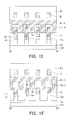
- FIG. 12 and FIG. 12 ′ each illustrate a cross-sectional view taken along the line IV-IV′ in FIG. 10 .
- FIG. 13 is the equivalent circuit of the layout shown in FIG. 10 .
- FIG. 14 illustrates a layout of a non-volatile memory device according to the third exemplary embodiment of the present invention.
- FIG. 15 illustrates a cross-sectional view taken along the line I-I′ in FIG. 14 .
- FIG. 16 illustrates a cross-sectional view taken along the line II-II′ in FIG. 14 .
- FIG. 17 is the equivalent circuit of the layout shown in FIG. 14 .
- FIG. 18 illustrates a cross-sectional view of the fourth exemplary embodiment taken along the line III-III′ in FIG. 3 .
- FIG. 19 illustrates a cross-sectional view of the fourth exemplary embodiment taken along the line IV-IV′ in FIG. 3 .
- FIG. 20 illustrates a cross-sectional view of the fourth exemplary embodiment taken along the line III-III′ in FIG. 3 .
- FIG. 21 illustrates a cross-sectional view of the fourth exemplary embodiment taken along the line IV-IV′ in FIG. 3 .
- FIG. 22 illustrates a cross-sectional view of the fourth exemplary embodiment taken along the line I-I′ in FIG. 3 .
- FIG. 23 illustrates a cross-sectional view of the fourth exemplary embodiment taken along the line II-II′ in FIG. 3 .
- FIG. 24 illustrates a cross-sectional view taken along the line I-I′ in FIG. 3 .
- FIG. 25 illustrates a cross-sectional view taken along the line II-II′ in FIG. 3 .
- FIG. 26 illustrates a cross-sectional view taken along the line III-III′ in FIG. 3 .
- FIG. 27 illustrates a cross-sectional view taken along the line IV-IV′ in FIG. 3 .
- FIG. 28 to FIG. 38 illustrate cross-sectional views of fabricating zigzag word lines taken along the line II-II′ in FIG. 3 .
- FIG. 39 to FIG. 46 illustrate cross-sectional views of fabricating zigzag bit lines taken along the line III-III′ in FIG. 3 .
- Capacitance Coupling Ratio (Cr) is an important factor to design a memory cell and is defined as follows.
- C OX is the capacitance across the tunnel oxide
- C IPD is the capacitance across the inter-poly dielectric layer.
- the capacitance across the inter-poly dielectric layer (C IPD ) must be larger than that across the tunnel oxide (C OX ). In other words, the capacitance coupling ration (Cr) is larger than 0.5.
- V FG C r V CG Eq. 2
- the reason of the word line delay is the parasitic resistance, which mainly comes from the capacitance between neighboring word lines.
- the distance between neighboring word lines is decreased with the device scaling of memory cells, as illustrated in FIG. 2 .
- the array of word lines at the upper lines is sparser than that at the bottom lines. Note that, there is no bit line contact between word lines in the NAND flash array, which is convenient to integrate more bits per unit area.
- the capacitance between neighboring word lines at the upper lines is smaller than that at the bottom lines. More parasitic capacitance exists at the bottom lines, because the distance between neighboring word lines is shorter.
- the distance between neighboring word lines may be increased. However, it appears that this is opposite to the device scaling of NAND flash with no bit line contact between cell transistors.
- the first key idea of this exemplary embodiment of the invention is to make the scaling of NAND cells consistent with the smallest cell area, by adopting the zigzag body word line wiring, as illustrated in FIG. 5 and FIG. 6 .
- FIG. 3 illustrates a layout of a non-volatile memory device according to the first exemplary embodiment of the present invention.
- Word lines WL-A and word lines WL-B are periodically arranged and extend in a first direction (e.g. the direction of row), while the bit lines BL-D and bit lines BL-E are periodically arranged and extend in a second direction (e.g. the direction of column).
- the second direction is different from the first direction.
- the second direction is perpendicular to the first direction.
- FIG. 4 is the equivalent circuit of the layout shown in FIG. 3 .
- FIG. 5 illustrates a cross-sectional view taken along the line I-I′ in FIG. 3 .
- word lines WL-A at a lower plane
- word lines WL-B at a higher plane
- neighboring word lines exist separately and are located respectively at higher and lower planes. Such disposition reduces the capacitance between neighboring word lines.
- the process of forming the structure of FIG. 5 will be described with reference to FIGS. 28-38 in the Sixth Exemplary embodiment.
- FIG. 6 illustrates a cross-sectional taken along the line II-II′ in FIG. 3 .
- word lines WL-A at a lower plane
- word lines WL-B at a higher plane
- neighboring word lines exist separately and are located respectively at higher and lower planes. Such disposition reduces the capacitance between neighboring word lines.
- neighboring bit lines exist separately and are located respectively at higher and lower planes.
- IPD thickness is periodically fluctuated between these two layers of WL-A and WL-B in both of FIG. 5 and FIG. 6 .
- the inter-poly dielectric films IPD-B below word lines WL-B are thicker than the inter-poly dielectric films IPD-A below word lines WL-A.
- the diffusion layers are omitted in figures, because they are not directly related to this invention.
- the non-volatile memory device includes: a well PW disposed in a substrate SUB; a plurality of first word lines WL-A and a plurality of second word lines WL-B disposed on the substrate SUB, arranged periodically and extending in a first direction; a plurality of inter-poly dielectric films IPD disposed on the plurality of floating gates FG and respectively beneath the plurality of first word lines WL-A and the plurality of second word lines WL-B; a plurality of floating gates FG disposed between the well PW and the plurality of inter-poly dielectric films IPD; and a plurality of tunnel oxide films TOX disposed between the well PW and the plurality of floating gates FG.
- the distance from the first word lines WL-A to the substrate SUB is smaller than the distance from the second word lines WL-B to the substrate SUB.
- the distance from the top of the first word lines WL-A to the substrate SUB is smaller than the distance from the bottom of the second word lines WL-B to the substrate SUB, but the invention is not limited thereto.
- the distance from the top of the first word lines WL-A to the substrate SUB can be equal to the distance from the bottom of the second word lines WL-B to the substrate SUB. This corresponds to the case that the line K-K′ and the line J-J′ are coincide in FIG. 24 and FIG. 25 .
- the plurality of inter-poly dielectric films IPD include a plurality of first inter-poly dielectric films IPD-A disposed on the plurality of floating gates FG and respectively beneath the first word lines WL-A; and a plurality of second inter-poly dielectric films IPD-B disposed on the substrate SUB and respectively beneath the second word lines WL-B.
- the thickness of the plurality of first inter-poly dielectric films IPD-A is smaller than the thickness of the plurality of second inter-poly dielectric films IPD-B.
- Cross-sectional views taken along the lines III-III′ and IV-IV′ in FIG. 3 are illustrated in FIG. 7 and FIG. 8 respectively.
- the plurality of floating gates FG include a plurality of first floating gates FG-A disposed on the tunnel oxide films TOX and respectively beneath the plurality of first word lines WL-A; and a plurality of second floating gates FG-B disposed on the tunnel oxide films TOX and respectively beneath the plurality of second word lines WL-B.
- the thickness of the plurality of first floating gates FG-A is smaller than the thickness of the plurality of second floating gates FG-B, as illustrated in FIG. 5 ′, FIG. 6 ′, FIG. 7 and FIG. 8 ′. In this event, IPD-A is thinner than IPD-B.
- the non-volatile memory device further includes a plurality of bit lines BL disposed above the first word lines WL-A and the second word lines WL-B and extending along a second direction different from the first direction.
- the plurality of bit lines BL include a plurality of first bit lines BL-E and a plurality of second bit lines BL-D, and the distance from the first bit lines BL-E to the substrate SUB is smaller than the distance from the second bit lines BL-D to the substrate SUB.
- the second key idea of this exemplary embodiment of the invention is the method for solving this issue. It will be described below.
- the capacitance coupling ratios (C rA and C rB ) below WL-A and WL-B are respectively determined as follows.
- the capacitance coupling ratio below WL-A is larger than that below WL-B.
- the voltage applied to the floating gate (or called self-potential of FG) is determined by the control gate voltage using Eq. 2.
- the self-potential of FG below WL-A (V FG-A ) and the self-potential of FG below WL-B (V FG-B ) are respectively determined by control gate voltages (V CG-A and V CG-B ).
- V FG-A C rA V CG-A Eq. 6
- V FG-B C rB V CG-B Eq. 7
- control gate voltages applied by WL-A and WL-B (V CG-A and V CG-B ) satisfy the following relationship.
- V CG - ⁇ B C rA C rB ⁇ V CG - A ⁇ V CG - A Eq . ⁇ 9
- the method for operating the said non-volatile memory device includes applying a first operating voltage to the first word lines WL-A; and applying a second operating voltage to the second word lines WL-B.
- the first operating voltage includes a first program voltage, a first erase voltage, a first pass voltage or a first read voltage.
- the second operating voltage includes a second program voltage, a second erase voltage, a second pass voltage or a second read voltage.
- the operating method further includes the following steps for programming the non-volatile memory device.
- a first program voltage V PGM-A is applied to a first word line WL-A
- a second program voltage V PGM-B is applied to a second word line WL-B.
- the self-potentials below WL-A and WL-B are respectively determined as follows.
- V FG-A C rA
- V FG-B C rB V PGM-B Eq. 10B
- V PGM-A is the first program voltage applied to a first word line WL-A
- V PGM-B is the second program voltage applied to a second word line WL-B
- C rA is a first capacitance coupling ratio determined by a ratio of a capacitance of the inter-poly dielectric film IPD-A to a sum of capacitances of the inter-poly dielectric film IPD-A and the tunnel oxide film
- C rB is a second capacitance coupling ratio determined by a ratio of a capacitance of the inter-poly dielectric film IPD-B to a sum of capacitances of the inter-poly dielectric film IPD-B and the tunnel oxide film.
- V PGM - B C rA C rB ⁇ V PGM - A ⁇ V PGM - A Eq . ⁇ 12
- the operating method further includes the following steps for erasing the entire non-volatile memory cells at the same moment (flash).
- a voltage V Pwell is applied to the P-well PW.
- the periodical difference with respect to WL-A and WL-B is taken into consideration.
- the self-potentials of FG below WL-A and WL-B (V FG-A and V FG-B ) are given with respect to WL-A and WL-B as follows.
- V FG-A ⁇ C rA ( V Pwell ⁇ V CG-A ) Eq. 13
- V FG-B ⁇ C rB ( V Pwell ⁇ V CG-B ) Eq. 14
- V Pwell cannot be selectively applied to memory cells under WL-A and WL-B, it is necessary to selectively apply V CG-A and V CG-B at the same moment.
- the first erase voltage V CG-A is applied to the first word lines WL-A
- the second erase voltage V CG-B is applied to the second word lines WL-B.
- C rA is a first capacitance coupling ratio determined by a ratio of a capacitance of the first inter-poly dielectric films to a sum of capacitances of the first inter-poly dielectric films and the tunnel oxide films
- C rB is a second capacitance coupling ratio determined by a ratio of a capacitance of the second inter-poly dielectric films to a sum of capacitances of the second inter-poly dielectric films and the tunnel oxide films
- V Pwell is the well voltage
- V CG-A is the first erase voltage applied to the first word lines
- V CG-B is the second erase voltage applied to the second word lines.
- V Pwell , V CG-A and V CG-B can be derived and V Pwell , V CG-A and V CG-B may satisfy the following equation during the erasing operation.
- V CG - B C rA C rB ⁇ V CG - A + ( 1 - C rA C rB ) ⁇ V Pwell Eq . ⁇ 16
- control gate voltage applied to WL-A (V CG-A ) is zero
- control gate voltage applied to WL-B (V CG-B ) is zero
- the operating method further includes the following steps for reading the non-volatile memory device having a plurality of cells. First, whether at least one cell to be read among the plurality of cells is connected with the first word lines WL-A or the second word lines WL-B is determined.
- the first read voltage V read-A is applied to the first word line WL-A connected with the cell to be read among the plurality of cells
- the first pass voltage V pass-A is applied to the other first word lines WL-A
- the second pass voltage V pass-B is applied to the second word lines WL-B.
- the second read voltage V read-B is applied to the second word line WL-B connected with the cell to be read among the plurality of cells
- the second pass voltage V pass-B is applied to the other second word line WL-B
- the first pass voltage V pass-A is applied to the first word lines WL-A.
- V pass-A and V pass-B are the pass voltages applied to WL-A and WL-B, respectively.
- V FG-A C rA V pass-A Eq. 19
- V FG-B C rB V pass-B Eq. 20
- C rA is a first capacitance coupling ratio determined by a ratio of a capacitance of the first inter-poly dielectric films to a sum of capacitances of the first inter-poly dielectric films and the tunnel oxide films
- C rB is a second capacitance coupling ratio determined by a ratio of a capacitance of the second inter-poly dielectric films to a sum of capacitances of the second inter-poly dielectric films and the tunnel oxide films
- V pass-A is the first pass voltage
- V pass-B is the second pass voltage.
- V pass - B C rA C rB ⁇ V pass - A Eq . ⁇ 22
- V pass-B is larger than V pass-A .
- V pass - B C rA C rB ⁇ V pass - A > V pass - A Eq . ⁇ 23
- V FG-B C rB V read-B Eq. 25
- C rA is a first capacitance coupling ratio determined by a ratio of a capacitance of the first inter-poly dielectric films to a sum of capacitances of the first inter-poly dielectric films and the tunnel oxide films
- C rB is a second capacitance coupling ratio determined by a ratio of a capacitance of the second inter-poly dielectric films to a sum of capacitances of the second inter-poly dielectric films and the tunnel oxide films
- V read-A is the first read voltage
- V read-B is the second read voltage.
- V read - B C rA C rB ⁇ V read - A Eq . ⁇ 27
- V read - B C rA C rB ⁇ V read - A > V read - A Eq . ⁇ 28
- FIG. 7 illustrates a cross-sectional view taken along the line III-III′ in FIG. 3 .
- bit lines BL-E at a lower plane
- bit lines BL-D at a higher plane
- neighboring bit lines exist separately and respectively at higher and lower planes. Such disposition reduces the capacitance between neighboring bit lines.
- FIG. 8 and FIG. 8 ′ each illustrate a cross-sectional view taken along the line IV-IV′ in FIG. 3 .
- bit lines BL-D at an upper plane
- bit lines BL-E at a lower plane
- neighboring bit lines exist separately and are located respectively at higher and lower planes. Such disposition reduces the capacitance between neighboring bit lines.
- FIG. 9 illustrates a cross-sectional view taken along the line V-V′ in FIG. 3 .
- bit lines BL-D at an upper plane
- bit lines BL-E at a lower plane
- the bit lines BL-D and BL-E are located in the insulating film INS.
- the non-volatile memory device includes: a well PW disposed in a substrate SUB; a plurality of word lines WL arranged in an array, disposed on the substrate SUB and extending in a first direction; a plurality of inter-poly dielectric films IPD respectively between the substrate SUB and the plurality of word lines WL; a plurality of floating gates FG respectively disposed between the well PW and the plurality inter-poly dielectric films IPD; a plurality of tunnel oxide films TOX respectively disposed between the well PW and the plurality of floating gates FG; and a plurality of first bit lines BL-E and a plurality of second bit lines BL-D arranged periodically, disposed over the plurality of word lines WL, and extending in a second direction, wherein the first direction is perpendicular to the second direction.
- the distance from the first bit lines BL-E to the substrate SUB is smaller than the distance from the second bit lines BL-D to the substrate SUB.
- the distance from the top of the first bit lines BL-E to the substrate SUB is smaller than the distance from the bottom of the second bit lines BL-D to the substrate SUB, but the invention is not limited thereto.
- the distance from the top of the first bit lines BL-E to the substrate SUB can be equal to the distance from the bottom of the second bit lines BL-D to the substrate SUB. This corresponds to the case that the line O-O′ and the line N-N′ are coincide in FIG. 26 and FIG. 27 .
- Word lines WL-A and word lines WL-B are periodically arranged and extend in a first direction (e.g. the direction of row), while the bit lines BL-D and bit lines BL-E are periodically arranged and extend in a second direction (e.g. the direction of column).
- the second direction is different from the first direction.
- the second direction is perpendicular to the first direction.
- FIG. 10 illustrates a layout of a non-volatile memory device according to the second exemplary embodiment of the present invention.
- the word lines WL-A and WL-B are periodically arranged in the direction of row, while the bit lines BL are homogenously arranged in the direction of column.
- the cross-sectional views taken along the lines I-I′ and II-II′ in FIG. 10 are similar to the cross-sectional view shown in FIG. 5 or FIG. 5 ′.
- the cross-sectional views taken along the lines III-III′ and IV-IV′ in FIG. 10 are illustrated in FIG. 11 and FIG. 12 , respectively.
- FIG. 13 is the equivalent circuit of the layout shown in FIG. 10 .
- the word lines WL-A and WL-B are periodically arranged in the direction of row, while the bit lines BL are arranged at the same plane in the direction of column.
- FIG. 14 illustrates a layout of a non-volatile memory device according to the third exemplary embodiment of the present invention.
- the word lines WL are homogeneously arranged in the direction of row, while the bit lines BL-D and BL-E are periodically arranged in the direction of column.
- the cross-sectional views taken along the lines III-III′ and IV-IV′ in FIG. 14 are similar to the cross-sectional view shown in FIG. 7 .
- the cross-sectional views taken along the lines I-I′ and II-II′ are illustrated in FIG. 15 and FIG. 16 , respectively.
- FIG. 17 is the equivalent circuit of the layout shown in FIG. 14 .
- the word lines WL are arranged at the same plane in the direction of row, while the bit lines BL-D and BL-E are periodically arranged in the direction of column.
- FIG. 18 illustrates a cross-sectional view of the fourth exemplary embodiment taken along the line III-III′ in FIG. 3 .
- a high-k material includes a dielectric material with a dielectric constant greater than 3.9.
- the high-k material is selected from the group consisting of metal oxide, metal nitride, metal silicide, transition metal oxide, transition metal nitride, transition metal salicide, metal oxynitride, metal aluminate, zirconium silicate, zirconium aluminate, and combinations thereof.
- the high-k material can include silicon oxide, silicon nitride, silicon oxynitride, hafnium oxide (HfO 2 ), zirconium oxide, titanium oxide, aluminum oxide, HfO 2 -alumina alloy, hafnium silicon oxide (HfSiO), hafnium silicon oxynitride (HfSiON), hafnium tantalum oxide (HfTaO), hafnium titanium oxide (HfTiO), hafnium zirconium oxide (HfZrO), Ta 2 O 5 , HfAlO X , or a combination thereof.
- FIG. 19 illustrates a cross-sectional view of the fourth exemplary embodiment taken along the line IV-IV′ in FIG. 3 .
- FIG. 20 illustrates a cross-sectional view of the fourth exemplary embodiment taken along the line III-III′ in FIG. 10 .
- FIG. 21 illustrates a cross-sectional view of the fourth exemplary embodiment taken along the line IV-IV′ in FIG. 10 .
- FIG. 22 illustrates a cross-sectional view of the fourth exemplary embodiment taken along the line I-I′ in FIG. 14 .
- FIG. 23 illustrates a cross-sectional view of the fourth exemplary embodiment taken along the line II-II′ in FIG. 14 .
- FIG. 24 illustrates a cross-sectional view taken along the line I-I′ in FIG. 3 .
- FIG. 25 illustrates a cross-sectional view taken along the line II-II′ in FIG. 3 .
- FIG. 26 illustrates a cross-sectional view taken along the line III-III′ in FIG. 3 .
- FIG. 27 illustrates a cross-sectional view taken along the line IV-IV′ in FIG. 3 .
- An exemplary embodiment is composed of plenty of layers stacked on the surface of a silicon substrate SUB at the line F-F′, as illustrated in FIG. 24 , FIG. 25 , FIG. 26 and FIG. 27 .
- the tops of tunnel oxide films TOX i.e. bottoms of floating gates FG
- the tops of floating gates FG are at the line H-H′.
- the tops of inter-poly dielectric films IPD-A are at the line I-I′.
- the tops of word lines WL-A are at the line J-J′.
- the tops of inter-poly dielectric films IPB-B are at the line K-K′.
- the tops of word lines WL-B are at the line L-L′.
- the bottoms of bit lines BL-E are at the line M-M′.
- the tops of bit lines BL-E are at the line N-N′.
- the bottoms of bit lines BL-D are at the line O-O′.
- the tops of bit lines BL-D are at the line P-P′.
- the line K-K′ is above the line J-J′, and the line O-O′ is above the line N-N′.
- This relationship between the lines K-K′, J-J′, O-O′ and N-N′ is common among the above-mentioned exemplary embodiments.
- FIG. 28 to FIG. 38 illustrate cross-sectional views of fabricating zigzag word lines taken along the line II-II′ in FIG. 3 .
- the fabrication process of zigzag word lines includes: forming a P-well (PW) in the substrate (SUB) and forming a poly-Si film (PSI), a dielectric film (DFA) and a metal film (MWA) on the substrate (SUB) ( FIG. 28 ); forming mask patterns (PR-A) on the metal film (MWA) ( FIG. 28 ); forming a spacer (SPA) on a sidewall of each mask pattern (PR-A) ( FIG.
- second trenches (TR 1 ) are formed through the metal film (MWA), the dielectric film (DFA) and the poly-Si film (PSI) ( FIG. 33 ); filling the second trenches (TR 1 ) with an insulating film (INS-A) ( FIG. 34 ); etching back a portion of the dielectric film (DFB), so as to form third trenches (TR 2 ) between the insulating films (INS-A) ( FIG. 35 ); forming a second metal film (MWB) in the third trenches (TR 2 ) ( FIG. 36 ); and removing a portion of the second metal film (MWB) outside of the trenches (TR 2 ), so as to form the second word line (WL-B) ( FIG. 37 ).
- mask patterns PR-A are formed on a metal film MWA for forming word lines WL-A.
- a first dielectric film DFA is formed below the metal film MWA and on a poly-Si film PSI for forming floating gates FG.
- An oxide film TOX for forming tunnel oxide films is formed below the poly-Si film PSI and on a Si substrate SUB.
- spacers SPA are formed as illustrated in FIG. 29 .
- the metal film MWA and the first dielectric film DFA are partially etched, so as to form trenches TR in the metal film MWA and in the first dielectric film DFA, as illustrated in FIG. 30 .
- a second dielectric film DFB for forming inter-poly films IPD-B is deposited to fill in the trenches TR, as illustrated in FIG. 31 .
- the spacers SPA are removed as illustrated in FIG. 32 .
- an etching is performed to the metal film MWA, the first dielectric film DFA and the poly-Si film PSI, by using the mask patterns PR-A as a mask, so as to expose a portion of the surface of the oxide film TOX, and thus, word lines WL-A, inter-poly dielectric films IP-A and floating gates FG are formed on the Si substrate SUB and trenches TR 1 are formed between the mask patterns PR-A and the second dielectric film DFB, as illustrated in FIG. 33 . And then, an interlayer insulating film INS-A is deposited to fill in the trenches TR 1 , as illustrated in FIG. 34 .
- the second dielectric film DFB is partially etched back by a selective etching, so as to form inter-poly films IPD-B and form trenches TR 2 between the interlayer insulating films INS-A, as illustrated in FIG. 35 .
- the inter-poly films IPD-B are beforehand incorporated with N.
- a metal film MWB for forming word lines WL-B is deposited on the Si substrate SUB filling in the trenches TR 2 . Subsequently, the metal film MWB outside of the trenches TR 2 is removed and thus word lines WL-B are left, as illustrated in FIG. 37 .
- bit lines BL-E are formed on the interlayer insulating film INS-B, as illustrated in FIG. 38 .
- FIG. 39 to FIG. 46 illustrate cross-sectional views of fabricating zigzag bit lines, taken along the line III-III′ in FIG. 3 .
- the fabrication process of zigzag bit lines includes: forming a metal film (MBE) and an interlayer insulating film (INS-B) on the word line (WL-A) ( FIG. 39 ); forming mask patterns (PR-B) on the metal film (MBE) ( FIG. 39 ); removing a portion of the metal film (MBE) by using the mask patterns (PR-B) as a mask, so as to form the first bit lines (BL-E), wherein first trenches (TR 3 ) are formed between the first bit lines (BL-E) ( FIG. 40 ); filling the first trenches (TR 3 ) with an insulating film (INS-C) ( FIG.
- MBE metal film
- INS-B interlayer insulating film
- mask patterns PR-B are formed on a metal film MBE for forming bit lines BL-E.
- the metal film MBE is formed on the surface of an interlayer insulating film INS-B.
- Word lines WL-A and word lines WL-B are formed below the interlayer insulating film INS-B.
- the metal film MBE is etched to form the bit lines BL-E and form trenches TR 3 between the bit lines BL-E, as illustrated in FIG. 40 .
- An insulating film INS-C is deposited into the trenches TR 3 , as illustrated in FIG. 41 .
- This insulating film INS-C is partially etched back by a selective etching, so that the top portion of each of the mask patterns PR-B is protruded from the surface of the remaining insulating film INS-C and trenches TR 4 are formed between the mask patterns PR-B, as illustrated in FIG. 42 .
- Bit lines BL-D are deposited on the surface of this insulating film INS-C respectively in the trenches TR 4 , as illustrated in FIG. 43 .
- the mask patterns PR-B are removed to form trenches TR 5 between the insulating films INS-C, as illustrated in FIG. 44 .
- the trenches TR 5 are buried in the interlayer insulating film INS-C.
- An interlayer insulating film INS-D is then deposited in the trenches TR 5 , as illustrated in FIG. 45 . Finally, the surfaces of bit lines BL-D and the surface of the interlayer insulating film INS-D are covered by an interlayer insulating film INS-E, as illustrated in FIG. 46 .
- the distance between neighboring word lines (or bit lines) can be increased by adopting the zigzag body wiring of the exemplary embodiment of the invention, so that the parasitic capacitance between neighboring word lines (or bit lines) can be suppressed.
- the zigzag body wiring of the exemplary embodiment of the invention is consistent with the scaling of NAND cells, so that the low bit cost can be achieved to meet the customers' requirement.
Landscapes
- Engineering & Computer Science (AREA)
- Microelectronics & Electronic Packaging (AREA)
- Non-Volatile Memory (AREA)
- Semiconductor Memories (AREA)
Abstract
Provided is a fabrication method of a non-volatile memory device having a zigzag body wiring. First word lines and second word lines are formed on a substrate, wherein the first word lines and the second word lines are arranged periodically and extend in a first direction. Bit lines are formed over the first and second word lines, wherein a first distance from the first word lines to the substrate is smaller than a second distance from the second word lines to the substrate.
Description
This application is a divisional application of U.S. application Ser. No. 13/969,626, filed on Aug. 19, 2013, now allowed. The entirety of the above-mentioned patent application is hereby incorporated by reference herein and made a part of this specification.
Field of the Invention
The present invention relates to a non-volatile memory device, and an operation method and a fabrication method thereof, and more particularly to a NAND flash memory having a zigzag body wiring, and an operation method and a fabrication method thereof.
Description of Related Art
In recent years, in order to overcome the issues of NAND flash scaling, emerging memories and three-dimensional memories have been aggressively investigated. With no happening, the delay of word lines and/or bit lines limits the development of a memory controller.
At the upper and lower lines in FIG. 1 , there are the cross-sections of bit lines. The distance between neighboring bit lines is wider at the upper lines than at the lower lines. The number of bit lines per unit space is larger at the lower, but the parasitic capacitance which causes the bit line delay exists. The self-align shallow trench isolation SA-STI, which is an important invention for the device scaling of NAND flash, greatly enhances the parasitic capacitance between neighboring bit lines. Therefore, the bit line delay has become notable with the scaling. At the upper and lower lines in FIG. 2 , there are the cross-sections of word lines. The distance between neighboring word lines is wider at the upper lines than at the lower lines. The number of word lines per unit space is larger at the lower, but the parasitic capacitance which causes the word line delay exists.
To lower the bit cost, the cell-to-cell space is shrunk as the memory cell is miniaturized. Accordingly, the parasitic capacitance between neighboring word lines is increased with the device scaling of NAND cells. Therefore, the word line delay has become notable with the scaling.
The present invention provides a non-volatile memory device, which includes: a well, disposed in a substrate; a plurality of first word lines and a plurality of second word lines, disposed on the substrate, arranged periodically and extending in a first direction; a plurality of inter-poly dielectric films, disposed on the substrate and respectively beneath the plurality of first word lines and the plurality of second word lines; a plurality of floating gates, disposed between the well and the plurality of inter-poly dielectric films; and a plurality of tunnel oxide films, disposed between the well and the plurality of floating gates, wherein a first distance from the first word lines to the substrate is smaller than a second distance from the second word lines to the substrate.
According to an exemplary embodiment of the present invention, a third distance from a top of the first word lines to the substrate is smaller than or equal to a fourth distance from a bottom of the second word lines to the substrate.
According to an exemplary embodiment of the present invention, the plurality of inter-poly dielectric films include a plurality of first inter-poly dielectric films disposed on the substrate and respectively beneath the first word lines, and a plurality of second inter-poly dielectric films disposed on the substrate and respectively beneath the second word lines, wherein a thickness of the plurality of first inter-poly dielectric films is smaller than a thickness of the plurality of second inter-poly dielectric films.
According to an exemplary embodiment of the present invention, the plurality of floating gates include a plurality of first floating gates disposed on the substrate and respectively beneath the plurality of first word lines, and a plurality of second floating gates disposed on the substrate and respectively beneath the plurality of second word lines, wherein a thickness of the plurality of first floating gates is smaller than a thickness of the plurality of second floating gates.
According to an exemplary embodiment of the present invention, the non-volatile memory device further includes a plurality of bit lines disposed above the first word lines and the second word lines and extending along a second direction different from the first direction.
According to an exemplary embodiment of the present invention, the plurality of bit lines include a plurality of first bit lines and a plurality of second bit lines, and a fifth distance from the first bit lines to the substrate is smaller than a sixth distance from the second bit lines to the substrate.
The present invention further provides a method for operating a non-volatile memory device having a substrate, a well, a plurality of first inter-poly dielectric films, a plurality of second inter-poly dielectric films, a plurality of first word lines and a plurality of second word lines disposed on the substrate and tunnel oxide films, wherein a first distance from the first word lines to the substrate being smaller than a second distance from the second word lines to the substrate. The method includes applying a first operating voltage to the first word lines, and applying a second operating voltage to the second word lines.
According to an exemplary embodiment of the present invention, wherein the first operating voltage includes a first program voltage, a first erase voltage, a first pass voltage or a first read voltage, and the second operating voltage includes a second program voltage, a second erase voltage, a second pass voltage or a second read voltage.
According to an exemplary embodiment of the present invention, the method further includes the following steps for programming the non-volatile memory device. The first program voltage is applied to a first word line, and the second program voltage is applied to a second word line. The first program voltage and the second program voltage satisfy the following equation:
C rA V PGM-A =C rB V PGM-B,
C rA V PGM-A =C rB V PGM-B,
wherein VPGM-A is the first program voltage applied to the first word line, VPGM-B is the second program voltage applied to the second word line, CrA is a first capacitance coupling ratio determined by a ratio of a capacitance of the first inter-poly dielectric films to a sum of capacitances of the first inter-poly dielectric films and the tunnel oxide films, and CrB is a second capacitance coupling ratio determined by a ratio of a capacitance of the second inter-poly dielectric films to a sum of capacitances of the second inter-poly dielectric films and the tunnel oxide films.
According to an exemplary embodiment of the present invention, the method further includes the following steps for erasing the non-volatile memory device. A well voltage is applied to the well, the first erase voltage is applied to the first word lines, and the second erase voltage is applied to the second word lines. The first erase voltage, the second erase voltage and the well voltage satisfy the following equation:
−C rA(V well −V CG-A)=−C rB(V well −V CG-B),
−C rA(V well −V CG-A)=−C rB(V well −V CG-B),
wherein CrA is a first capacitance coupling ratio determined by a ratio of a capacitance of the first inter-poly dielectric films to a sum of capacitances of the first inter-poly dielectric films and the tunnel oxide films, CrB is a second capacitance coupling ratio determined by a ratio of a capacitance of the second inter-poly dielectric films to a sum of capacitances of the second inter-poly dielectric films and the tunnel oxide films, Vwell is the well voltage, VCG-A is the first erase voltage applied to the first word lines, and VCG-B is the second erase voltage applied to the second word lines.
According to an exemplary embodiment of the present invention, the method further includes the following steps for reading the non-volatile memory device having a plurality of cells. Whether at least one cell to be read among the plurality of cells is connected with a first word line or a second word line is determined. If the at least one cell to be read among the plurality of cells is connected with a first word line, the first read voltage is applied to the first word line connected with the at least one cell to be read among the plurality of cells, the first pass voltage is applied to the other first word lines, and the second pass voltage is applied to the second word lines. If the at least one cell to be read among the plurality of cells is connected with a second word line, the second read voltage is applied to the second word line connected with the at least one cell to be read among the plurality of cells, the second pass voltage is applied to the other second word lines, and the first pass voltage is applied to the first word lines.
According to an exemplary embodiment of the present invention, the first pass voltage and the second pass voltage satisfy the following equation:
C rA V pass-A =C rB V pass-B,
C rA V pass-A =C rB V pass-B,
wherein CrA is a first capacitance coupling ratio determined by a ratio of a capacitance of the first inter-poly dielectric films to a sum of capacitances of the first inter-poly dielectric films and the tunnel oxide films, CrB is a second capacitance coupling ratio determined by a ratio of a capacitance of the second inter-poly dielectric films to a sum of capacitances of the second inter-poly dielectric films and the tunnel oxide films, Vpass-A is the first pass voltage, and Vpass-B is the second pass voltage.
According to an exemplary embodiment of the present invention, the first read voltage and the second read voltage satisfy the following equation:
C rA V read-A =C rB V read-B,
C rA V read-A =C rB V read-B,
wherein CrA is a first capacitance coupling ratio determined by a ratio of a capacitance of the first inter-poly dielectric films to a sum of capacitances of the first inter-poly dielectric films and the tunnel oxide films, CrB is a second capacitance coupling ratio determined by a ratio of a capacitance of the second inter-poly dielectric films to a sum of capacitances of the second inter-poly dielectric films and the tunnel oxide films, Vread-A is the first read voltage, and Vread-B is the second read voltage.
The present invention also provides a non-volatile memory device, which includes: a well, disposed in a substrate; a plurality of word lines, arranged in an array, disposed on the substrate and extending in a first direction; a plurality of inter-poly dielectric films respectively between the substrate and the plurality of word lines; a plurality of floating gates, respectively disposed between the well and the plurality of inter-poly dielectric films; a plurality of tunnel oxide films, respectively disposed between the well and the plurality of floating gates; and a plurality of first bit lines and a plurality of second bit lines, arranged periodically, disposed over the plurality of word lines, and extending in a second direction, wherein a first distance from the first bit lines to the substrate is smaller than a second distance from the second bit lines to the substrate.
According to an exemplary embodiment of the present invention, a third distance from a top of the first bit lines to the substrate is smaller than or equal to a fourth distance from a bottom of the second bit lines to the substrate.
According to an exemplary embodiment of the present invention, the first direction is perpendicular to the second direction.
The present invention further provides a fabrication method of a non-volatile memory device, which includes: forming a plurality of first word lines and a plurality of second word lines on a substrate, wherein the first word lines and the second word lines are arranged periodically and extend in a first direction; and forming a plurality of bit lines over the first and second word lines, wherein a first distance from the first word lines to the substrate is smaller than a second distance from the second word lines to the substrate.
According to an exemplary embodiment of the present invention, a third distance from a top of the first word lines to the substrate is smaller than or equal to a fourth distance from a bottom of the second word lines to the substrate.
According to an exemplary embodiment of the present invention, the step of forming a plurality of bit lines includes forming a plurality of first bit lines and a plurality of second bit lines, wherein the first bit lines and the second bit lines are arranged periodically and extend in a second direction different from the first direction, wherein a fifth distance from the first bit lines to the substrate is smaller than a sixth distance from the second bit lines to the substrate.
According to an exemplary embodiment of the present invention, a seventh distance from a top of the first bit lines to the substrate is smaller than or equal to an eighth distance from a bottom of the second bit lines to the substrate.
Reference now is made to the accompanying drawings to describe the specific exemplary embodiments and examples of the invention. Whenever possible, the same reference numbers are used in the drawings and the description to refer to the same or like parts.
Capacitance Coupling Ratio (Cr) is an important factor to design a memory cell and is defined as follows.
where COX is the capacitance across the tunnel oxide and CIPD is the capacitance across the inter-poly dielectric layer. To make sure the controllability of a control gate on channel, the capacitance across the inter-poly dielectric layer (CIPD) must be larger than that across the tunnel oxide (COX). In other words, the capacitance coupling ration (Cr) is larger than 0.5.
The self-potential of the floating gate (VFG) is determined by this Cr as follows.
V FG =C r V CG Eq. 2
V FG =C r V CG Eq. 2
From this equation, it is found that the word line delay (same with VCG delay) causes the voltage actually applied to the floating gate (VFG) to be fluctuated.
The reason of the word line delay is the parasitic resistance, which mainly comes from the capacitance between neighboring word lines. The distance between neighboring word lines is decreased with the device scaling of memory cells, as illustrated in FIG. 2 . The array of word lines at the upper lines is sparser than that at the bottom lines. Note that, there is no bit line contact between word lines in the NAND flash array, which is convenient to integrate more bits per unit area. The capacitance between neighboring word lines at the upper lines is smaller than that at the bottom lines. More parasitic capacitance exists at the bottom lines, because the distance between neighboring word lines is shorter.
To suppress the parasitic capacitance, the distance between neighboring word lines may be increased. However, it appears that this is opposite to the device scaling of NAND flash with no bit line contact between cell transistors.
Zigzag Body Word Line
The first key idea of this exemplary embodiment of the invention is to make the scaling of NAND cells consistent with the smallest cell area, by adopting the zigzag body word line wiring, as illustrated in FIG. 5 and FIG. 6 .
However, it is noted that IPD thickness is periodically fluctuated between these two layers of WL-A and WL-B in both of FIG. 5 and FIG. 6 . The inter-poly dielectric films IPD-B below word lines WL-B are thicker than the inter-poly dielectric films IPD-A below word lines WL-A. For the ease of recognition, the diffusion layers are omitted in figures, because they are not directly related to this invention.
In view of the above, the non-volatile memory device includes: a well PW disposed in a substrate SUB; a plurality of first word lines WL-A and a plurality of second word lines WL-B disposed on the substrate SUB, arranged periodically and extending in a first direction; a plurality of inter-poly dielectric films IPD disposed on the plurality of floating gates FG and respectively beneath the plurality of first word lines WL-A and the plurality of second word lines WL-B; a plurality of floating gates FG disposed between the well PW and the plurality of inter-poly dielectric films IPD; and a plurality of tunnel oxide films TOX disposed between the well PW and the plurality of floating gates FG. Besides, the distance from the first word lines WL-A to the substrate SUB is smaller than the distance from the second word lines WL-B to the substrate SUB. In this embodiment, the distance from the top of the first word lines WL-A to the substrate SUB is smaller than the distance from the bottom of the second word lines WL-B to the substrate SUB, but the invention is not limited thereto. In another embodiment, the distance from the top of the first word lines WL-A to the substrate SUB can be equal to the distance from the bottom of the second word lines WL-B to the substrate SUB. This corresponds to the case that the line K-K′ and the line J-J′ are coincide in FIG. 24 and FIG. 25 .
In addition, the plurality of inter-poly dielectric films IPD include a plurality of first inter-poly dielectric films IPD-A disposed on the plurality of floating gates FG and respectively beneath the first word lines WL-A; and a plurality of second inter-poly dielectric films IPD-B disposed on the substrate SUB and respectively beneath the second word lines WL-B. Besides, the thickness of the plurality of first inter-poly dielectric films IPD-A is smaller than the thickness of the plurality of second inter-poly dielectric films IPD-B. Cross-sectional views taken along the lines III-III′ and IV-IV′ in FIG. 3 are illustrated in FIG. 7 and FIG. 8 respectively.
Moreover, the plurality of floating gates FG include a plurality of first floating gates FG-A disposed on the tunnel oxide films TOX and respectively beneath the plurality of first word lines WL-A; and a plurality of second floating gates FG-B disposed on the tunnel oxide films TOX and respectively beneath the plurality of second word lines WL-B. Besides, the thickness of the plurality of first floating gates FG-A is smaller than the thickness of the plurality of second floating gates FG-B, as illustrated in FIG. 5 ′, FIG. 6 ′, FIG. 7 and FIG. 8 ′. In this event, IPD-A is thinner than IPD-B.
The non-volatile memory device further includes a plurality of bit lines BL disposed above the first word lines WL-A and the second word lines WL-B and extending along a second direction different from the first direction. The plurality of bit lines BL include a plurality of first bit lines BL-E and a plurality of second bit lines BL-D, and the distance from the first bit lines BL-E to the substrate SUB is smaller than the distance from the second bit lines BL-D to the substrate SUB.
The second key idea of this exemplary embodiment of the invention is the method for solving this issue. It will be described below.
Accordingly, the capacitance coupling ratios (CrA and CrB) below WL-A and WL-B are respectively determined as follows.
Since the inter-poly dielectric films IPD-B are thicker than the inter-poly dielectric films IPD-A, the capacitance coupling ratio below WL-A is larger than that below WL-B.
The voltage applied to the floating gate (or called self-potential of FG) is determined by the control gate voltage using Eq. 2.
In this exemplary embodiment of the invention, the self-potential of FG below WL-A (VFG-A) and the self-potential of FG below WL-B (VFG-B) are respectively determined by control gate voltages (VCG-A and VCG-B).
V FG-A =C rA V CG-A Eq. 6
V FG-B =C rB V CG-B Eq. 7
V FG-A =C rA V CG-A Eq. 6
V FG-B =C rB V CG-B Eq. 7
It should be noted that it is preferred to control the self-potentials (VFG-A and VFG-B) in a uniform manner regardless of WL-A and WL-B, while there is a periodical difference between WL-A and WL-B. The condition for this is written in the following equation.
C rA V CG-A =C rB V CG-B Eq. 8
C rA V CG-A =C rB V CG-B Eq. 8
This means that the control gate voltages applied by WL-A and WL-B (VCG-A and VCG-B) satisfy the following relationship.
The method for operating the said non-volatile memory device is described in the following. The operating method includes applying a first operating voltage to the first word lines WL-A; and applying a second operating voltage to the second word lines WL-B. The first operating voltage includes a first program voltage, a first erase voltage, a first pass voltage or a first read voltage. The second operating voltage includes a second program voltage, a second erase voltage, a second pass voltage or a second read voltage.
Programming Operation
The operating method further includes the following steps for programming the non-volatile memory device. To program, a first program voltage VPGM-A is applied to a first word line WL-A, and subsequently a second program voltage VPGM-B is applied to a second word line WL-B. In this event, the self-potentials below WL-A and WL-B are respectively determined as follows.
V FG-A =C rA V PGM-A Eq. 10A
V FG-B =C rB V PGM-B Eq. 10B
V FG-A =C rA V PGM-A Eq. 10A
V FG-B =C rB V PGM-B Eq. 10B
To control the self-potentials (VFG-A and VFG-B) in a uniform manner regardless of WL-A and WL-B, the following equation must be satisfied. The first program voltage VFG-A and the second program voltage VFG-B satisfy the following equation:
C rA V PGM-A =C rB V PGM-B Eq. 11
C rA V PGM-A =C rB V PGM-B Eq. 11
wherein VPGM-A is the first program voltage applied to a first word line WL-A, VPGM-B is the second program voltage applied to a second word line WL-B, CrA is a first capacitance coupling ratio determined by a ratio of a capacitance of the inter-poly dielectric film IPD-A to a sum of capacitances of the inter-poly dielectric film IPD-A and the tunnel oxide film, and CrB is a second capacitance coupling ratio determined by a ratio of a capacitance of the inter-poly dielectric film IPD-B to a sum of capacitances of the inter-poly dielectric film IPD-B and the tunnel oxide film.
As a result, it is found that the program voltages in this exemplary embodiment of the invention are periodically changing with regard to WL-A and WL-B as follows.
Erasing Operation
The operating method further includes the following steps for erasing the entire non-volatile memory cells at the same moment (flash). A voltage VPwell is applied to the P-well PW. Secondly, the periodical difference with respect to WL-A and WL-B is taken into consideration. In this event, the self-potentials of FG below WL-A and WL-B (VFG-A and VFG-B) are given with respect to WL-A and WL-B as follows.
V FG-A =−C rA(V Pwell −V CG-A) Eq. 13
V FG-B =−C rB(V Pwell −V CG-B) Eq. 14
V FG-A =−C rA(V Pwell −V CG-A) Eq. 13
V FG-B =−C rB(V Pwell −V CG-B) Eq. 14
Since the voltage VPwell cannot be selectively applied to memory cells under WL-A and WL-B, it is necessary to selectively apply VCG-A and VCG-B at the same moment. The first erase voltage VCG-A is applied to the first word lines WL-A, and the second erase voltage VCG-B is applied to the second word lines WL-B. To make the self-potentials in a unique manner regardless of WL-A and WL-B, the following condition must be satisfied. The first erase voltage VCG-A, the second erase voltage VCG-B and the well voltage VPwell satisfy the following equation:
−C rA(V Pwell −V CG-A)=−C rB(V Pwell −V CG-B) Eq. 15
−C rA(V Pwell −V CG-A)=−C rB(V Pwell −V CG-B) Eq. 15
wherein CrA is a first capacitance coupling ratio determined by a ratio of a capacitance of the first inter-poly dielectric films to a sum of capacitances of the first inter-poly dielectric films and the tunnel oxide films, CrB is a second capacitance coupling ratio determined by a ratio of a capacitance of the second inter-poly dielectric films to a sum of capacitances of the second inter-poly dielectric films and the tunnel oxide films, VPwell is the well voltage, VCG-A is the first erase voltage applied to the first word lines, and VCG-B is the second erase voltage applied to the second word lines.
The relationship among VPwell, VCG-A and VCG-B can be derived and VPwell, VCG-A and VCG-B may satisfy the following equation during the erasing operation.
In the event that the control gate voltage applied to WL-A (VCG-A) is zero, the control gate voltage applied to WL-B (VCG-B) and the voltage VPwell have the following relationship.
In the event that the control gate voltage applied to WL-B (VCG-B) is zero, the control gate voltage applied to WL-A (VCG-A) and the voltage VPwell have the following relationship.
Reading Operation
The operating method further includes the following steps for reading the non-volatile memory device having a plurality of cells. First, whether at least one cell to be read among the plurality of cells is connected with the first word lines WL-A or the second word lines WL-B is determined.
If at least one cell to be read among the plurality of cells is connected with a first word line WL-A, the first read voltage Vread-A is applied to the first word line WL-A connected with the cell to be read among the plurality of cells, the first pass voltage Vpass-A is applied to the other first word lines WL-A, and the second pass voltage Vpass-B is applied to the second word lines WL-B. If at least one cell to be read among the plurality of cells is connected with a second word line WL-B, the second read voltage Vread-B is applied to the second word line WL-B connected with the cell to be read among the plurality of cells, the second pass voltage Vpass-B is applied to the other second word line WL-B, and the first pass voltage Vpass-A is applied to the first word lines WL-A.
Specifically, to read a selected cell in a NAND string, pass voltage is applied to the word line connected to the other cells than the cell to be read. The self-potentials of floating gates not to be read while reading the selected cell are respectively written as follows, wherein Vpass-A and Vpass-B are the pass voltages applied to WL-A and WL-B, respectively.
V FG-A =C rA V pass-A Eq. 19
V FG-B =C rB V pass-B Eq. 20
V FG-A =C rA V pass-A Eq. 19
V FG-B =C rB V pass-B Eq. 20
To make the self-potentials of non-selected cells same, the following equation may be satisfied.
C rA V pass-A =C rB V pass-B Eq. 21
C rA V pass-A =C rB V pass-B Eq. 21
wherein CrA is a first capacitance coupling ratio determined by a ratio of a capacitance of the first inter-poly dielectric films to a sum of capacitances of the first inter-poly dielectric films and the tunnel oxide films, CrB is a second capacitance coupling ratio determined by a ratio of a capacitance of the second inter-poly dielectric films to a sum of capacitances of the second inter-poly dielectric films and the tunnel oxide films, Vpass-A is the first pass voltage, and Vpass-B is the second pass voltage.
In this event, the following condition may be satisfied.
Since CrA is larger than CrB in this example, Vpass-B is larger than Vpass-A.
To read the selected cell, the read voltage is applied to the selected cell. If the selected cell is connected to WL-A, the self-potential of the floating gate of the selected cell is determined by the following equation.
V FG-A =C rA V read-A Eq. 24
V FG-A =C rA V read-A Eq. 24
If the selected cell is connected to WL-B, the self-potential of the floating gate of the selected cell is determined by the following equation.
V FG-B =C rB V read-B Eq. 25
V FG-B =C rB V read-B Eq. 25
To make the self-potentials of the selected cells same regardless of WL-A and WL-B, the following equation may be satisfied.
C rA V read-A =C rB V read-B Eq. 26
C rA V read-A =C rB V read-B Eq. 26
wherein CrA is a first capacitance coupling ratio determined by a ratio of a capacitance of the first inter-poly dielectric films to a sum of capacitances of the first inter-poly dielectric films and the tunnel oxide films, CrB is a second capacitance coupling ratio determined by a ratio of a capacitance of the second inter-poly dielectric films to a sum of capacitances of the second inter-poly dielectric films and the tunnel oxide films, Vread-A is the first read voltage, and Vread-B is the second read voltage.
From this equation, it is preferable to change the read voltages with respect to WL-A and WL-B.
In this example, since CrA is larger than CrB, the following condition may be satisfied.
Zigzag Bit Line Wiring
With the scaling of NAND flash, the distance between neighboring bit lines is shrunk, as illustrated in FIG. 1 . To suppress the increase in the parasitic capacitance between them, a zigzag body bit line wiring shall be useful.
In view of the above, the non-volatile memory device includes: a well PW disposed in a substrate SUB; a plurality of word lines WL arranged in an array, disposed on the substrate SUB and extending in a first direction; a plurality of inter-poly dielectric films IPD respectively between the substrate SUB and the plurality of word lines WL; a plurality of floating gates FG respectively disposed between the well PW and the plurality inter-poly dielectric films IPD; a plurality of tunnel oxide films TOX respectively disposed between the well PW and the plurality of floating gates FG; and a plurality of first bit lines BL-E and a plurality of second bit lines BL-D arranged periodically, disposed over the plurality of word lines WL, and extending in a second direction, wherein the first direction is perpendicular to the second direction. Besides, the distance from the first bit lines BL-E to the substrate SUB is smaller than the distance from the second bit lines BL-D to the substrate SUB. In this embodiment, the distance from the top of the first bit lines BL-E to the substrate SUB is smaller than the distance from the bottom of the second bit lines BL-D to the substrate SUB, but the invention is not limited thereto. In another embodiment, the distance from the top of the first bit lines BL-E to the substrate SUB can be equal to the distance from the bottom of the second bit lines BL-D to the substrate SUB. This corresponds to the case that the line O-O′ and the line N-N′ are coincide in FIG. 26 and FIG. 27 .
Word lines WL-A and word lines WL-B are periodically arranged and extend in a first direction (e.g. the direction of row), while the bit lines BL-D and bit lines BL-E are periodically arranged and extend in a second direction (e.g. the direction of column). The second direction is different from the first direction. In this exemplary embodiment, the second direction is perpendicular to the first direction.
High-k IPD
An exemplary embodiment is composed of plenty of layers stacked on the surface of a silicon substrate SUB at the line F-F′, as illustrated in FIG. 24 , FIG. 25 , FIG. 26 and FIG. 27 . The tops of tunnel oxide films TOX (i.e. bottoms of floating gates FG) are at the line G-G′ above the line F-F′. The tops of floating gates FG are at the line H-H′. The tops of inter-poly dielectric films IPD-A are at the line I-I′. The tops of word lines WL-A are at the line J-J′. The tops of inter-poly dielectric films IPB-B are at the line K-K′. The tops of word lines WL-B are at the line L-L′. The bottoms of bit lines BL-E are at the line M-M′. The tops of bit lines BL-E are at the line N-N′. The bottoms of bit lines BL-D are at the line O-O′. The tops of bit lines BL-D are at the line P-P′.
In the exemplary embodiment of the invention, the line K-K′ is above the line J-J′, and the line O-O′ is above the line N-N′. This relationship between the lines K-K′, J-J′, O-O′ and N-N′ is common among the above-mentioned exemplary embodiments.
A fabrication process of zigzag word lines is described in the following. FIG. 28 to FIG. 38 illustrate cross-sectional views of fabricating zigzag word lines taken along the line II-II′ in FIG. 3 .
In an exemplary embodiment, the fabrication process of zigzag word lines includes: forming a P-well (PW) in the substrate (SUB) and forming a poly-Si film (PSI), a dielectric film (DFA) and a metal film (MWA) on the substrate (SUB) (FIG. 28 ); forming mask patterns (PR-A) on the metal film (MWA) (FIG. 28 ); forming a spacer (SPA) on a sidewall of each mask pattern (PR-A) (FIG. 29 ); removing a portion of the metal film (MWA) by using the mask patterns (PR-A) and the spacers (SPA) as a mask, so as to form first trenches (TR) through the metal film (MWA) and the dielectric film (DFA) (FIG. 30 ); filling the first trenches (TR) with a dielectric film (DFB) (FIG. 31 ); removing the spacers (SPA) (FIG. 32 ); removing another portion of the metal film (MWA) by using the mask patterns (PR-A) as a mask, so as to form the first word lines, wherein second trenches (TR1) are formed through the metal film (MWA), the dielectric film (DFA) and the poly-Si film (PSI) (FIG. 33 ); filling the second trenches (TR1) with an insulating film (INS-A) (FIG. 34 ); etching back a portion of the dielectric film (DFB), so as to form third trenches (TR2) between the insulating films (INS-A) (FIG. 35 ); forming a second metal film (MWB) in the third trenches (TR2) (FIG. 36 ); and removing a portion of the second metal film (MWB) outside of the trenches (TR2), so as to form the second word line (WL-B) (FIG. 37 ).
Referring to FIG. 28 , mask patterns PR-A are formed on a metal film MWA for forming word lines WL-A. A first dielectric film DFA is formed below the metal film MWA and on a poly-Si film PSI for forming floating gates FG. An oxide film TOX for forming tunnel oxide films is formed below the poly-Si film PSI and on a Si substrate SUB.
After forming spacers SPA as illustrated in FIG. 29 , the metal film MWA and the first dielectric film DFA are partially etched, so as to form trenches TR in the metal film MWA and in the first dielectric film DFA, as illustrated in FIG. 30 . Next, a second dielectric film DFB for forming inter-poly films IPD-B is deposited to fill in the trenches TR, as illustrated in FIG. 31 . Subsequently, the spacers SPA are removed as illustrated in FIG. 32 .
Subsequently, an etching is performed to the metal film MWA, the first dielectric film DFA and the poly-Si film PSI, by using the mask patterns PR-A as a mask, so as to expose a portion of the surface of the oxide film TOX, and thus, word lines WL-A, inter-poly dielectric films IP-A and floating gates FG are formed on the Si substrate SUB and trenches TR1 are formed between the mask patterns PR-A and the second dielectric film DFB, as illustrated in FIG. 33 . And then, an interlayer insulating film INS-A is deposited to fill in the trenches TR1, as illustrated in FIG. 34 .
The second dielectric film DFB is partially etched back by a selective etching, so as to form inter-poly films IPD-B and form trenches TR2 between the interlayer insulating films INS-A, as illustrated in FIG. 35 . To do this, for example, the inter-poly films IPD-B are beforehand incorporated with N.
In FIG. 36 , a metal film MWB for forming word lines WL-B is deposited on the Si substrate SUB filling in the trenches TR2. Subsequently, the metal film MWB outside of the trenches TR2 is removed and thus word lines WL-B are left, as illustrated in FIG. 37 .
The surfaces of the word lines WL-B, the surfaces of the mask patterns PR-A and the surface of the interlayer insulating film INS-A are covered by an interlayer insulating film INS-B, and then bit lines BL-E are formed on the interlayer insulating film INS-B, as illustrated in FIG. 38 .
A fabrication process of zigzag bit lines is described in the following. FIG. 39 to FIG. 46 illustrate cross-sectional views of fabricating zigzag bit lines, taken along the line III-III′ in FIG. 3 .
In an exemplary embodiment, the fabrication process of zigzag bit lines includes: forming a metal film (MBE) and an interlayer insulating film (INS-B) on the word line (WL-A) (FIG. 39 ); forming mask patterns (PR-B) on the metal film (MBE) (FIG. 39 ); removing a portion of the metal film (MBE) by using the mask patterns (PR-B) as a mask, so as to form the first bit lines (BL-E), wherein first trenches (TR3) are formed between the first bit lines (BL-E) (FIG. 40 ); filling the first trenches (TR3) with an insulating film (INS-C) (FIG. 41 ); etching back a portion of the insulating film (INS-C), so as to form second trenches (TR4) between the mask patterns (PR-B) (FIG. 42 ); forming the second bit lines (BL-D) in the second trenches (TR4) (FIG. 43 ); removing the mask patterns (PR-B), so as to form third trenches (TR5) between the insulating films (INS-C) (FIG. 44 ); and filling the third trenches (TR5) with another insulating film (INS-D) (FIG. 45 ).
In FIG. 39 , mask patterns PR-B are formed on a metal film MBE for forming bit lines BL-E. The metal film MBE is formed on the surface of an interlayer insulating film INS-B. Word lines WL-A and word lines WL-B (not shown but similar to WL-A) are formed below the interlayer insulating film INS-B.
Using the mask patterns PR-B as a mask, the metal film MBE is etched to form the bit lines BL-E and form trenches TR3 between the bit lines BL-E, as illustrated in FIG. 40 . An insulating film INS-C is deposited into the trenches TR3, as illustrated in FIG. 41 .
This insulating film INS-C is partially etched back by a selective etching, so that the top portion of each of the mask patterns PR-B is protruded from the surface of the remaining insulating film INS-C and trenches TR4 are formed between the mask patterns PR-B, as illustrated in FIG. 42 .
Bit lines BL-D are deposited on the surface of this insulating film INS-C respectively in the trenches TR4, as illustrated in FIG. 43 . Subsequently, the mask patterns PR-B are removed to form trenches TR5 between the insulating films INS-C, as illustrated in FIG. 44 . The trenches TR5 are buried in the interlayer insulating film INS-C.
An interlayer insulating film INS-D is then deposited in the trenches TR5, as illustrated in FIG. 45 . Finally, the surfaces of bit lines BL-D and the surface of the interlayer insulating film INS-D are covered by an interlayer insulating film INS-E, as illustrated in FIG. 46 .
In summary, the distance between neighboring word lines (or bit lines) can be increased by adopting the zigzag body wiring of the exemplary embodiment of the invention, so that the parasitic capacitance between neighboring word lines (or bit lines) can be suppressed. In addition, the zigzag body wiring of the exemplary embodiment of the invention is consistent with the scaling of NAND cells, so that the low bit cost can be achieved to meet the customers' requirement.
The present invention has been disclosed above in the exemplary embodiments, but is not limited to those. It is known to persons skilled in the art that some modifications and innovations may be made without departing from the spirit and the scope of the present invention. Therefore, the scope of the present invention may be defined by the following claims.
Claims (3)
1. A fabrication method of a non-volatile memory device, comprising:
forming a plurality of first floating gates and a plurality of second floating gates on a substrate;
forming a plurality of first dielectric films and second dielectric films on the substrate;
forming a plurality of first word lines and a plurality of second word lines on the substrate, wherein the first word lines and the second word lines are arranged periodically and extend in a first direction, each of the first dielectric films is located between each of the first floating gates and each of the first word lines, each of the second dielectric films is located between each of the second floating gates and each of the second word lines, and a first thickness of each of the first dielectric films is less than a second thickness of each of the second dielectric films; and
forming a plurality of bit lines over the first and second word lines,
wherein a first distance from a top of the first word lines to the substrate is smaller than a second distance from a bottom of the second word lines to the substrate, and
wherein a third thickness of the first floating gate is less than fourth thickness of the second floating gate.
2. The fabrication method of claim 1 , wherein the step of forming a plurality of bit lines comprises forming a plurality of first bit lines and a plurality of second bit lines, wherein the first bit lines and the second bit lines are arranged periodically and extend in a second direction different from the first direction,
wherein a third distance from the first bit lines to the substrate is smaller than a fourth distance from the second bit lines to the substrate.
3. The fabrication method of claim 2 , wherein a fifth distance from a top of the first bit lines to the substrate is smaller than or equal to an sixth distance from a bottom of the second bit lines to the substrate.
Priority Applications (1)
| Application Number | Priority Date | Filing Date | Title |
|---|---|---|---|
| US14/704,986 US10026644B2 (en) | 2013-08-19 | 2015-05-06 | Fabricating method of non-volatile memory device |
Applications Claiming Priority (2)
| Application Number | Priority Date | Filing Date | Title |
|---|---|---|---|
| US13/969,626 US9064968B2 (en) | 2013-08-19 | 2013-08-19 | Non-volatile memory device and operation and fabricating methods thereof |
| US14/704,986 US10026644B2 (en) | 2013-08-19 | 2015-05-06 | Fabricating method of non-volatile memory device |
Related Parent Applications (1)
| Application Number | Title | Priority Date | Filing Date |
|---|---|---|---|
| US13/969,626 Division US9064968B2 (en) | 2013-08-19 | 2013-08-19 | Non-volatile memory device and operation and fabricating methods thereof |
Publications (2)
| Publication Number | Publication Date |
|---|---|
| US20150235893A1 US20150235893A1 (en) | 2015-08-20 |
| US10026644B2 true US10026644B2 (en) | 2018-07-17 |
Family
ID=52466736
Family Applications (3)
| Application Number | Title | Priority Date | Filing Date |
|---|---|---|---|
| US13/969,626 Active 2033-10-04 US9064968B2 (en) | 2013-08-19 | 2013-08-19 | Non-volatile memory device and operation and fabricating methods thereof |
| US14/704,986 Active 2034-01-28 US10026644B2 (en) | 2013-08-19 | 2015-05-06 | Fabricating method of non-volatile memory device |
| US14/704,982 Active US9123578B1 (en) | 2013-08-19 | 2015-05-06 | Non-volatile memory device |
Family Applications Before (1)
| Application Number | Title | Priority Date | Filing Date |
|---|---|---|---|
| US13/969,626 Active 2033-10-04 US9064968B2 (en) | 2013-08-19 | 2013-08-19 | Non-volatile memory device and operation and fabricating methods thereof |
Family Applications After (1)
| Application Number | Title | Priority Date | Filing Date |
|---|---|---|---|
| US14/704,982 Active US9123578B1 (en) | 2013-08-19 | 2015-05-06 | Non-volatile memory device |
Country Status (3)
| Country | Link |
|---|---|
| US (3) | US9064968B2 (en) |
| CN (1) | CN104425502B (en) |
| TW (1) | TWI517308B (en) |
Families Citing this family (5)
| Publication number | Priority date | Publication date | Assignee | Title |
|---|---|---|---|---|
| JP2016062624A (en) * | 2014-09-17 | 2016-04-25 | 株式会社東芝 | Semiconductor memory device |
| CN106445404B (en) * | 2015-08-13 | 2019-04-23 | 群联电子股份有限公司 | Memory programming method, memory control circuit unit and memory storage device |
| US10163494B1 (en) * | 2017-05-31 | 2018-12-25 | Taiwan Semiconductor Manufacturing Co., Ltd. | Memory device and fabrication method thereof |
| CN109817624B (en) * | 2019-01-22 | 2020-09-25 | 上海华虹宏力半导体制造有限公司 | Memory and operation method thereof |
| US11557537B2 (en) * | 2020-08-06 | 2023-01-17 | Micron Technology, Inc. | Reduced pitch memory subsystem for memory device |
Citations (5)
| Publication number | Priority date | Publication date | Assignee | Title |
|---|---|---|---|---|
| US6137178A (en) * | 1998-06-17 | 2000-10-24 | Siemens Aktiengesellschaft | Semiconductor metalization system and method |
| US20020004297A1 (en) * | 1996-10-31 | 2002-01-10 | Manny Ma | Advance metallization process |
| US20070198766A1 (en) * | 2006-02-22 | 2007-08-23 | Kabushiki Kaisha Toshiba | Semiconductor memory and method for manufacturing a semiconductor memory |
| US20070247906A1 (en) * | 2006-03-28 | 2007-10-25 | Hiroshi Watanabe | Fin type memory cell |
| US7737554B2 (en) * | 2007-06-25 | 2010-06-15 | Taiwan Semiconductor Manufacturing Company, Ltd. | Pitch by splitting bottom metallization layer |
Family Cites Families (5)
| Publication number | Priority date | Publication date | Assignee | Title |
|---|---|---|---|---|
| US6005270A (en) * | 1997-11-10 | 1999-12-21 | Sony Corporation | Semiconductor nonvolatile memory device and method of production of same |
| KR100668350B1 (en) * | 2005-12-20 | 2007-01-12 | 삼성전자주식회사 | NAND structured multi-bit nonvolatile memory device and manufacturing method thereof |
| JP4300228B2 (en) * | 2006-08-28 | 2009-07-22 | 株式会社東芝 | Nonvolatile semiconductor memory device |
| JP4594921B2 (en) * | 2006-12-18 | 2010-12-08 | 株式会社東芝 | Method for manufacturing nonvolatile semiconductor device |
| KR100875538B1 (en) * | 2007-02-27 | 2008-12-26 | 삼성전자주식회사 | Nonvolatile memory device and its program and erase method |
-
2013
- 2013-08-19 US US13/969,626 patent/US9064968B2/en active Active
- 2013-12-26 TW TW102148485A patent/TWI517308B/en active
- 2013-12-31 CN CN201310756464.0A patent/CN104425502B/en active Active
-
2015
- 2015-05-06 US US14/704,986 patent/US10026644B2/en active Active
- 2015-05-06 US US14/704,982 patent/US9123578B1/en active Active
Patent Citations (5)
| Publication number | Priority date | Publication date | Assignee | Title |
|---|---|---|---|---|
| US20020004297A1 (en) * | 1996-10-31 | 2002-01-10 | Manny Ma | Advance metallization process |
| US6137178A (en) * | 1998-06-17 | 2000-10-24 | Siemens Aktiengesellschaft | Semiconductor metalization system and method |
| US20070198766A1 (en) * | 2006-02-22 | 2007-08-23 | Kabushiki Kaisha Toshiba | Semiconductor memory and method for manufacturing a semiconductor memory |
| US20070247906A1 (en) * | 2006-03-28 | 2007-10-25 | Hiroshi Watanabe | Fin type memory cell |
| US7737554B2 (en) * | 2007-06-25 | 2010-06-15 | Taiwan Semiconductor Manufacturing Company, Ltd. | Pitch by splitting bottom metallization layer |
Also Published As
| Publication number | Publication date |
|---|---|
| US9064968B2 (en) | 2015-06-23 |
| CN104425502B (en) | 2017-05-24 |
| US20150235893A1 (en) | 2015-08-20 |
| TW201508868A (en) | 2015-03-01 |
| CN104425502A (en) | 2015-03-18 |
| US20150236033A1 (en) | 2015-08-20 |
| US9123578B1 (en) | 2015-09-01 |
| US20150049557A1 (en) | 2015-02-19 |
| TWI517308B (en) | 2016-01-11 |
Similar Documents
| Publication | Publication Date | Title |
|---|---|---|
| US12207460B2 (en) | Method of manufacturing semiconductor device having a subtrate with a protruding portion having different heights in regions overlapped with different gate electrodes | |
| US12022651B2 (en) | Flash memory structure with enhanced floating gate | |
| US7795080B2 (en) | Methods of forming integrated circuit devices using composite spacer structures | |
| CN107527915B (en) | Storage devices | |
| US9698156B2 (en) | Vertical thin-channel memory | |
| US7026684B2 (en) | Nonvolatile semiconductor memory device | |
| US7736973B2 (en) | Non-volatile memory arrays having dual control gate cell structures and a thick control gate dielectric and methods of forming | |
| US20100065900A1 (en) | Semiconductor device including resistance element | |
| CN106558590A (en) | Memory element and manufacturing method thereof | |
| CN107634065A (en) | Memory device | |
| US10026644B2 (en) | Fabricating method of non-volatile memory device | |
| JP4504403B2 (en) | Semiconductor memory device | |
| US7388784B2 (en) | Nonvolatile semiconductor memory device including memory cell units each having a given number of memory cell transistors | |
| US8248859B2 (en) | Methods of forming and operating NAND memory with side-tunneling | |
| KR20070111877A (en) | Non-volatile memory integrated circuit device and manufacturing method thereof | |
| US20070132001A1 (en) | Non-volatile memory and manufacturing method and operating method thereof | |
| US7512005B2 (en) | NAND memory with side-tunneling | |
| US8017477B2 (en) | Nonvolatile memory devices and methods of fabricating the same | |
| US20080123433A1 (en) | Flash memory device and method of manufacturing the same | |
| US20080099824A1 (en) | Flash memory device and method of fabricating the same | |
| US20080048244A1 (en) | Nonvolatile memory, nonvolatile memory array and manufacturing method thereof | |
| JP2008166415A (en) | Semiconductor device and manufacturing method thereof |
Legal Events
| Date | Code | Title | Description |
|---|---|---|---|
| STCF | Information on status: patent grant |
Free format text: PATENTED CASE |
|
| MAFP | Maintenance fee payment |
Free format text: PAYMENT OF MAINTENANCE FEE, 4TH YEAR, LARGE ENTITY (ORIGINAL EVENT CODE: M1551); ENTITY STATUS OF PATENT OWNER: LARGE ENTITY Year of fee payment: 4 |
|
| MAFP | Maintenance fee payment |
Free format text: PAYMENT OF MAINTENANCE FEE, 8TH YEAR, LARGE ENTITY (ORIGINAL EVENT CODE: M1552); ENTITY STATUS OF PATENT OWNER: LARGE ENTITY Year of fee payment: 8 |