US10025439B2 - Virtual sensor mirroring for circular touch panels - Google Patents
Virtual sensor mirroring for circular touch panels Download PDFInfo
- Publication number
- US10025439B2 US10025439B2 US15/090,578 US201615090578A US10025439B2 US 10025439 B2 US10025439 B2 US 10025439B2 US 201615090578 A US201615090578 A US 201615090578A US 10025439 B2 US10025439 B2 US 10025439B2
- Authority
- US
- United States
- Prior art keywords
- adjustment parameter
- sensor
- virtual
- virtual sensor
- corner
- Prior art date
- Legal status (The legal status is an assumption and is not a legal conclusion. Google has not performed a legal analysis and makes no representation as to the accuracy of the status listed.)
- Active, expires
Links
Images


Classifications
-
- G—PHYSICS
- G06—COMPUTING OR CALCULATING; COUNTING
- G06F—ELECTRIC DIGITAL DATA PROCESSING
- G06F3/00—Input arrangements for transferring data to be processed into a form capable of being handled by the computer; Output arrangements for transferring data from processing unit to output unit, e.g. interface arrangements
- G06F3/01—Input arrangements or combined input and output arrangements for interaction between user and computer
- G06F3/03—Arrangements for converting the position or the displacement of a member into a coded form
- G06F3/041—Digitisers, e.g. for touch screens or touch pads, characterised by the transducing means
- G06F3/044—Digitisers, e.g. for touch screens or touch pads, characterised by the transducing means by capacitive means
-
- G—PHYSICS
- G06—COMPUTING OR CALCULATING; COUNTING
- G06F—ELECTRIC DIGITAL DATA PROCESSING
- G06F3/00—Input arrangements for transferring data to be processed into a form capable of being handled by the computer; Output arrangements for transferring data from processing unit to output unit, e.g. interface arrangements
- G06F3/01—Input arrangements or combined input and output arrangements for interaction between user and computer
- G06F3/03—Arrangements for converting the position or the displacement of a member into a coded form
- G06F3/041—Digitisers, e.g. for touch screens or touch pads, characterised by the transducing means
- G06F3/0416—Control or interface arrangements specially adapted for digitisers
- G06F3/04166—Details of scanning methods, e.g. sampling time, grouping of sub areas or time sharing with display driving
-
- G—PHYSICS
- G06—COMPUTING OR CALCULATING; COUNTING
- G06F—ELECTRIC DIGITAL DATA PROCESSING
- G06F3/00—Input arrangements for transferring data to be processed into a form capable of being handled by the computer; Output arrangements for transferring data from processing unit to output unit, e.g. interface arrangements
- G06F3/01—Input arrangements or combined input and output arrangements for interaction between user and computer
- G06F3/03—Arrangements for converting the position or the displacement of a member into a coded form
- G06F3/041—Digitisers, e.g. for touch screens or touch pads, characterised by the transducing means
- G06F3/0416—Control or interface arrangements specially adapted for digitisers
- G06F3/0418—Control or interface arrangements specially adapted for digitisers for error correction or compensation, e.g. based on parallax, calibration or alignment
-
- G—PHYSICS
- G06—COMPUTING OR CALCULATING; COUNTING
- G06F—ELECTRIC DIGITAL DATA PROCESSING
- G06F3/00—Input arrangements for transferring data to be processed into a form capable of being handled by the computer; Output arrangements for transferring data from processing unit to output unit, e.g. interface arrangements
- G06F3/01—Input arrangements or combined input and output arrangements for interaction between user and computer
- G06F3/03—Arrangements for converting the position or the displacement of a member into a coded form
- G06F3/041—Digitisers, e.g. for touch screens or touch pads, characterised by the transducing means
- G06F3/044—Digitisers, e.g. for touch screens or touch pads, characterised by the transducing means by capacitive means
- G06F3/0446—Digitisers, e.g. for touch screens or touch pads, characterised by the transducing means by capacitive means using a grid-like structure of electrodes in at least two directions, e.g. using row and column electrodes
Definitions
- the disclosed implementations relate generally to touch-sensitive displays, and in particular, to computing touch centroids for touches on a non-rectangular touch-sensitive display.
- Computing devices such as notebook computers, personal digital assistants, mobile communication devices, portable entertainment devices (e.g., handheld video game devices, multimedia players) may include user interface devices that facilitate interaction between a user and the computing device.
- portable entertainment devices e.g., handheld video game devices, multimedia players
- a capacitance sensing system may include a touch screen, a touch-sensor pad, a touch-sensor slider, or touch-sensor buttons, and may include an array of one or more capacitive sensor elements (also referred to as sensor electrodes).
- Capacitive sensing typically involves measuring, through sensor signals (e.g., increases or decreases in electrode responses), a change in capacitance associated with the capacitive sensor elements to determine a presence of a conductive object (e.g., a user's finger or a stylus) relative to the capacitive sensor elements.
- Changes in capacitance are measured across arrays of sensors when they are used for sensing and processing capacitive touch applications. Because the “changes” are measured, changing information (AC or delta information) is desired in order to detect variation in capacitance, while constant information (DC or signal offset) is not desired. The DC component is rejected.
- a touch on a touch sensitive display typically spans multiple sensors to varying degrees.
- Various algorithms are used to identify the “location” of the touch based on the multiple sensor readings. Some algorithms identify a sensor whose capacitance change is a local maximum. Some techniques construct a centroid for the touch, and may use a local maximum to identify a small region for analysis (e.g., a 3 ⁇ 3 or 5 ⁇ 5 grid around the local maximum).
- Disclosed implementations of systems, methods, and devices address the problems associated with computing touch centroids for touches near the edge of a touch sensor array.
- the techniques disclosed can be applied to circular or other non-rectangular arrays of touch sensors.
- a touch sensing system includes a two-dimensional capacitive sense array.
- the capacitive sense array includes a plurality of capacitive sensors, which are typically arranged in a rectangular shape.
- the two-dimensional array is non-rectangular (e.g., circular).
- Each capacitive sensor in the capacitive sense array is associated with a unique location type.
- the location types are core, inner edge, outer edge, outer corner, and inner corner.
- the touch sensing system includes a capacitance measurement circuit coupled to the capacitive sense array.
- the capacitance measurement circuit is configured to measure capacitance changes at each capacitive sensor of the capacitive sense array.
- the touch sensing system also includes a memory device that stores three or more adjustment parameters. Each adjustment parameter corresponds to one or more of the location types, and is used in computing virtual sensor values.
- the touch sensing system also includes a processing unit coupled to the capacitance measurement circuit.
- the processing unit is configured to receive measured capacitance changes corresponding to a touch on the capacitive sense array and to identify a first capacitive sensor whose measured capacitance change is a local maximum within the capacitance sense array.
- the processing unit determines a first location type of the first sensor. In accordance with the first location type, the adjustment parameters corresponding to the first location type, and the measured capacitance changes, the processing unit computes a plurality of virtual sensor measurements. The processing unit then computes a centroid of the touch using a plurality of the measured capacitance changes and the plurality of virtual sensor measurements.
- the adjustment parameters include a first adjustment parameter for inner edges, a second adjustment parameter for outer edges, and a plurality of additional adjustment parameters for corners.
- the plurality of additional adjustment parameters for corners include an inner corner adjustment parameter, an outer corner adjustment parameter, an edge corner adjustment parameter, and a corner adjustment parameter.
- a method is performed at a touch sensing system that includes a capacitive sense array and one or more processing devices coupled to the capacitive sense array.
- the processing devices are configured to perform any of the methods described herein.
- a non-transitory computer-readable storage medium stores one or more programs configured for execution by one or more processors of a touch sensing system.
- the one or more programs include instructions for performing any of the methods described herein.
- the disclosed techniques increase both the accuracy and linearity of touch calculations.
- FIG. 1 is a block diagram illustrating a sensing system, in accordance with various implementations.
- FIG. 2 is a diagram illustrating a touch sensing array including a substrate having a capacitive sense array (e.g., a touch screen), in accordance with various implementations.
- a capacitive sense array e.g., a touch screen
- FIG. 3 is a block diagram illustrating an implementation of a management module.
- FIG. 4 illustrates location types for sensors in a rectangular array in accordance with some implementations.
- FIGS. 5A-5E illustrate a local maximum (“LM”) capacitance measurement at various locations within a rectangular array, in accordance with some implementations.
- LM local maximum
- FIGS. 6A-6E illustrate a process for calculating virtual sensor (“VS”) measurements at a corner of a rectangular array, in accordance with some implementations.
- VS virtual sensor
- FIGS. 7A-7C illustrate a process for calculating virtual sensor measurements at an outer edge of a rectangular array, in accordance with some implementations.
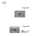
- FIGS. 8A and 8B illustrate a process for calculating virtual sensor measurements at an inner edge of a rectangular array, in accordance with some implementations.
- FIG. 9 illustrates location types for sensors in a non-rectangular array in accordance with some implementations.
- FIGS. 10A and 10B provide tables of parameters that are used in calculating virtual sensor measurements in accordance with some implementations.
- FIGS. 11A-11D illustrate a process for calculating virtual sensor measurements at an inner edge of a non-rectangular array, in accordance with some implementations.
- FIGS. 12A-12D illustrate a process for calculating virtual sensor measurements at an outer edge of a non-rectangular array, in accordance with some implementations.
- FIGS. 13A-13F illustrate a process for calculating virtual sensor measurements at a corner (also referred to as an outer corner) of a non-rectangular array, in accordance with some implementations.
- FIGS. 14A-14F illustrate a process for calculating virtual sensor measurements at an inner corner of a non-rectangular array, in accordance with some implementations.
- FIGS. 15A and 15B illustrate applying the disclosed techniques to sensors that are laid out in a circular pattern, in accordance with some implementations.
- FIG. 1 is a block diagram illustrating a sensing system 100 , in accordance with various implementations. While some example features are illustrated, various other features have not been illustrated for the sake of brevity and so as not to obscure pertinent aspects of the example implementations disclosed herein. To that end, as a non-limiting example, sensing system 100 includes a processing device 120 (also sometimes called a touch sensitive device), which includes a touch controller 124 and a touch screen 130 (also sometimes called a touch sensitive display), and is used in conjunction with or includes a computer system 110 (e.g., a host system or a host computer).
- a processing device 120 also sometimes called a touch sensitive device
- touch controller 124 includes a touch controller 124 and a touch screen 130 (also sometimes called a touch sensitive display)
- computer system 110 e.g., a host system or a host computer.
- the sensing system 100 provides the functionality of a touch screen, a touchpad, a slider, a button, a switch, a level sensor, a proximity sensor, a displacement sensor, a combination thereof, or provides some other functionality based on a detection of a user input.
- the touch screen provides the functionality of a proximity sensor.
- the computer system 110 is coupled to the touch controller 124 through data connections 101 .
- the computer system 110 includes the touch controller 124 , or a portion of the touch controller 124 , as a component and/or as a subsystem.
- some or all of the functionality of the touch controller 124 is implemented by software executed on the computer system 110 .
- the computer system 110 may be any suitable computer device, such as a laptop computer, a tablet device, a netbook, a personal digital assistant, a mobile phone, a smart phone, a gaming device, a computer server, or any other computing device.
- the computer system 110 is sometimes called a host or a host system.
- the computer system 110 includes one or more processors, one or more types of memory, a display and/or other user interface components such as a keyboard, a touch-screen display, a mouse, a track-pad, a digital camera, and/or any number of supplemental I/O devices to add functionality to computer system 110 .
- the touch screen 130 is coupled to the touch controller 124 through the connections 103 .
- the touch controller 124 and the touch screen 130 are included in the same device (i.e., an integrated electronic device) as components thereof.
- the touch controller 124 and the touch screen 130 are embedded in a host device (e.g., computer system 110 ), such as a mobile device, tablet, other computer or computer controlled device, and the methods described herein are performed, at least in part, by the embedded the touch controller.
- the touch screen 130 includes a sensing array 132 (e.g., a capacitive sense array) that forms a touch sensitive display.
- the sensing array 132 includes one or more of light-sensitive elements, light emitting elements, photosensitive elements, pressure sensitive elements, and/or capacitive sensor elements (also referred to as sensor electrodes).
- the capacitive sensor elements are electrodes of conductive material, such as copper.
- the sensing array 132 is sensitive to an input object 134 at a location 136 (e.g., a user's finger).
- a touch controller 124 includes a management module 121 - 1 , a host interface 129 , a touch screen interface 128 , and additional module(s) 125 .
- the touch controller 124 may include various additional features that have not been illustrated for the sake of brevity and so as not to obscure pertinent features of the example implementations disclosed herein, and a different arrangement of features may be possible.
- the host interface 129 provides an interface to the computer system 110 through the data connections 101 .
- the touch screen interface 128 provides an interface to the touch screen 130 though the connections 103 .
- a management module 121 - 1 (also referred to as sensing module) includes one or more processing units 122 - 1 (sometimes herein called CPUs, processors, or hardware processors, and sometimes implemented using microprocessors, microcontrollers, or the like) configured to detect (or process), via the sensing array 132 , a presence of one or more input objects 134 proximate or in contact with one or more sensor electrodes of the sensing array 132 .
- the management module 121 - 1 performs operations (e.g., scan operations) to sense, via the sensing array 132 , signals indicating the presence of the one or more input objects (e.g., input object 134 ).
- the management module 121 - 1 detects a pressure applied to the touch screen 130 , light (e.g., infrared light) associated with an input object, an image associated with an input object, a capacitance of the sensors and/or a change in capacitance of one or more of the sensor electrodes of the sensing array 132 when an input object is proximate to or in contact with the touch screen 130 .
- the sensing ability of the sensing module 121 - 1 depends on the type of sensors used in the touch screen 130 (e.g., capacitance sensors such as self-capacitance sensors and/or mutual-capacitance sensors).
- the one or more CPUs 122 - 1 of the management module 121 - 1 are shared by one or more components within, and in some cases, beyond the function of touch controller 124 .
- the management module 121 - 1 is coupled to the host interface 129 , the additional module(s) 125 , and the touch screen interface 128 in order to coordinate the operation of these components.
- one or more modules of management module 121 - 1 are implemented in the management module 121 - 2 of the computer system 110 .
- one or more processors of computer system 110 (not shown) are configured to execute instructions in one or more programs (e.g., in the management module 121 - 2 ).
- the management module 121 - 2 is coupled to the processing device 120 in order to manage the operation of the processing device 120 .
- the additional module(s) 125 are coupled to the touch screen interface 128 , the host interface 129 , and the management module 121 - 1 .
- the additional module(s) 125 may include a memory module (e.g., random access memory and/or flash memory).
- the memory module stores detected electrode responses, electrode response criteria, previously determined baselines, and the like.
- the additional module(s) 125 include analog and/or digital general purpose input/output (“GPIO”) ports 107 .
- the GPIO ports are coupled to a Programmable Interconnect and Logic (“PIL”), which acts as an interconnect between GPIO ports and a digital block array of the processing device 120 .
- PIL Programmable Interconnect and Logic
- the digital block array may be configurable to implement a variety of digital logic circuits (e.g., DACs, digital filters, or digital control systems) using, in one implementation, configurable user modules (“Ums”).
- the additional module(s) 125 include an analog block array that is used to implement a variety of analog circuits.
- the analog block array may also be coupled to the GPIO ports.
- FIG. 2 is a diagram illustrating a touch sensing array 200 (e.g., the touch screen 130 in FIG. 1 ) including a substrate 201 (e.g., a dielectric material) having a capacitive sense array 202 (e.g., the sensing array 132 in FIG. 1 ), in accordance with various implementations.
- FIG. 2 includes rows R 0 -R 9 210 and columns C 0 -C 9 220 of sensor elements (e.g., sensor elements 204 -A, 204 -B) arranged in an array.
- each of the rows R 0 -R 9 210 and columns C 0 -C 9 220 of sensor elements are coupled with a sensing module (e.g., a management module 121 - 1 ).
- a sensing module e.g., a management module 121 - 1
- each of the rows R 0 -R 9 210 and columns C 0 -C 9 220 of sensor elements may operate as both transmit and receive electrodes.
- the plurality of sensor electrodes 204 includes both self-capacitance sensors and mutual-capacitance sensors.
- each of the rows R 0 -R 9 210 of the sensor elements 204 crosses with each of the columns C 0 -C 9 220 of the sensor elements 204 . In this way, galvanic isolation is maintained between the rows R 0 -R 9 210 and the columns C 0 -C 9 220 .
- each of the columns C 0 -C 9 220 are associated with an X-coordinate or range of X-coordinates of the X-Y plane and each of the rows R 0 -R 9 210 are associated with a Y-coordinate or range of Y-coordinates of the X-Y plane.
- the sensing module can determine a location (e.g., the touch location 136 in FIG. 1 ) of a touch 206 on the capacitive sense array 202 using X and Y coordinates of the touch 206 .
- the plurality of sensor electrodes 204 are shown to be diamond shaped, one or more of the sensor elements 204 may be formed of other shapes (e.g., lines, stripes, bars, triangles, snowflakes, and/or any other shape) and be organized in various other patterns (e.g., intersections, concentric circles, saw tooth pattern, Manhattan pattern, and/or other patterns) without departing from the claimed subject matter.
- the sensor elements 204 cover all or a portion of the surface area of the substrate 201 .
- the sensor elements 204 and patterns of the sensor elements 204 are formed on or through one or more layers on the substrate 201 .
- a processing device measures capacitance of the plurality of sensor electrodes 204 using self-capacitance sensing.
- self-capacitance sensing measures added (or subtracted) capacitance at each of the plurality of sensor electrodes 204 .
- a user's touch e.g., a finger
- the processing device detects a “touch” when the added capacitance to the specific sensor electrode, relative to a baseline, exceeds a predefined threshold.
- the processing device measures capacitance of the plurality of sensor electrodes 204 using mutual-capacitance sensing.
- mutual-capacitance sensing measures capacitance between a column electrode (e.g., a transmitter (TX) electrode), and a row electrode (e.g., a receiver (RX) electrode).
- TX transmitter
- RX receiver
- mutual-capacitance sensing measures a change (e.g., a decrease or increase) in capacitance between the column electrode and the row electrode resulting from a user's touch.
- FIG. 3 is a block diagram illustrating an implementation of a management module.
- the management module 121 - 1 typically includes one or more processing units 302 for executing modules, programs, and/or instructions stored in memory 306 and thereby performing processing operations, memory 306 and one or more communication buses 308 for interconnecting these components.
- the communication buses 308 optionally include circuitry (sometimes called a chipset) that interconnects and controls communications between system components.
- the management module 121 - 1 is coupled to a touch screen by the communication buses 308 and the touch screen interface 128 .
- the memory 306 , or the computer readable storage medium of the memory 306 stores the following modules and data used by the modules:
- the scan module 312 uses a multiplexer or switch matrix (not shown) to distribute signals to one or more sensor electrodes. In some implementations, the scan module 312 uses the same or a different multiplexer (not shown) to receive current from the one or more sensor electrodes. This configuration allows the scan module 312 to scan all or specific portions of the capacitive sense array. In some implementations, scanning specific portions of the capacitive sense array (e.g., corner portions) consumes less energy compared to scanning the entire capacitive sensor array.
- Each of the above identified elements may be stored in one or more of the previously mentioned memory devices that together form the memory 306 , and corresponds to a set of instructions for performing a function described above.
- the above identified modules or programs i.e., sets of instructions
- the memory 306 may store a subset of the modules and data structures identified above.
- the memory 306 may store additional modules and data structures not described above.
- the memory 306 stores detected electrode responses, electrode response criterions, previously determined baselines, the water detection algorithm, the wipe detection algorithm, and other relevant information.
- the programs, modules, and data structures stored in memory 306 , or the computer readable storage medium of the memory 306 provide instructions for implementing respective operations in the methods described herein.
- FIG. 4 illustrates location types for sensors in a rectangular array in accordance with some implementations.
- the central sensors are labeled as “core.” These are the sensors that are at least two sensors away from any edge. There are four “corners” and four rows/columns of outer edge sensors. In addition, there is a rectangular ring of “inner edge” sensors that are adjacent to the outer edge.
- centroid for a touch depends on whether the finger location is at a Corner, an OuterEdge, an InnerEdge, or the Core area. For the core area, it is reasonably easy to compute a centroid because there are enough surrounding sensor readings. To report reasonable edge/corner coordinates at other locations, implementations use a virtual sensor mirroring technique.
- VS is used to represent a Virtual Sensor
- LM is used to identify a Local Maximum (where the finger is located)
- AS is used to identify an Actual Sensor. Note that an LM sensor is a special case of an actual sensor AS.
- FIGS. 5A-5E illustrate a local maximum (“LM”) capacitance measurement at various locations within a rectangular array, in accordance with some implementations.
- FIG. 5A illustrates the local maximum at a corner of outer edges 502 and 504
- FIG. 5B illustrates the local maximum on an outer edge 506
- FIG. 5C illustrates the local maximum on a outer edge 508
- FIG. 5D illustrates the local maximum on an inner edge 510
- FIG. 5E illustrates the local maximum on an inner edge 512 .
- FIGS. 6A-6E illustrate a process for calculating virtual sensor measurements at a corner of a rectangular array, in accordance with some implementations.
- the local maximum LM is at the center of a 5 ⁇ 5 grid, which includes both virtual sensors and actual sensors.
- FIG. 6A the rows and columns are labeled 0-4 in the grid, and each element is referenced by [row, column].
- the bottom left virtual sensor in FIG. 6A is VS[4,0].
- the sequence of FIGS. 6A-6E illustrates one way to populate the values of the virtual sensors in sequence.
- virtual sensors that are adjacent to actual sensors are computed using a first adjustment parameter, which is sometimes referred to as the Inner Edge Gain.
- VS ⁇ [ 1 , j ] AS ⁇ [ 2 , j ] * Inner ⁇ ⁇ Edge ⁇ ⁇ Gain 128 Note that AS[2,2] is equivalent to LM. Next, populate VS[2,1], VS[3,1], VS[4,1], which is
- the denominator is shown as 128 , but this is just an example.
- FIG. 6C illustrates that the next calculation is for V[1,1]. Specifically,
- VS ⁇ [ 1 , 1 ] VS ⁇ [ 1 , 2 ] + VS ⁇ [ 2 , 1 ] 2
- VS ⁇ [ 0 , 0 ] VS ⁇ [ 1 , 0 ] + VS ⁇ [ 0 , 1 ] 2
- FIGS. 7A-7C illustrate a process for calculating virtual sensor measurements at an outer edge of a rectangular array, in accordance with some implementations.
- FIGS. 8A and 8B illustrate a process for calculating virtual sensor measurements at an inner edge of a rectangular array, in accordance with some implementations.
- FIG. 9 illustrates location types for sensors in a non-rectangular array in accordance with some implementations.
- Corner sometimes referred to as an “Outer Corner”
- InnerCorner the Core sensors have at least two actual sensors on all sides, so no virtual sensors are needed in order to compute a centroid using a 5 ⁇ 5 grid.
- various virtual sensor measurement are computed, including:
- Some implementations compute these virtual sensor values using the six adjustment parameters listed in FIG. 10A , including Inner Edge Gain, Outer Edge Gain, Edge Corner Gain, Corner Gain, Inner Corner Gain, and Outer Corner Gain. These parameters are used depending on the location of the local maximum LM and the location of the virtual sensor relative to the other sensors, as illustrated in FIG. 10B .
- the table in FIG. 10B indicates which adjustment parameters are used depending on the location of the sensor, and this is described in more detail below in FIGS. 11A-11D, 12A-12D, 13A-13F , and 14 A- 14 F.
- FIGS. 11A-11D illustrate a process for calculating virtual sensor measurements at an inner edge of a non-rectangular array, in accordance with some implementations.
- FIG. 11A illustrates 8 different arrangements that have an inner edge sensor as the local maximum LM. Based on horizontal, vertical, and/or diagonal mirroring, each of the arrangements is equivalent to the first arrangement 1100 , which is described in FIGS. 11B-11D .
- FIG. 11B illustrates the starting point, with 6 virtual sensors not yet calculated.
- the first sensor to calculate is the virtual sensor VS[0,1], which in some implementations is computed as:
- VS ⁇ [ i , 0 ] AS ⁇ [ i , 1 ] * InnerEdgeGain 128 where i ranges from 0 to 4.
- FIGS. 12A-12D illustrate a process for calculating virtual sensor measurements at an outer edge of a non-rectangular array, in accordance with some implementations.
- FIG. 12A illustrates 8 different arrangements that have an outer edge sensor as the local maximum LM. Based on horizontal, vertical, and/or diagonal mirroring, each of the arrangements is equivalent to the first arrangement 1200 , which is described in FIGS. 12B-12D .
- FIG. 12B illustrates the starting point, with 11 virtual sensors not yet calculated.
- the first sensor to calculate is the virtual sensor VS[0,2], which in some implementations is computed as:
- the virtual sensors VS[0,0] to VS[4,0] are computed, as illustrated by the grid 1204 in FIG. 12D .
- the values are computed using the formula
- FIGS. 13A-13F illustrate a process for calculating virtual sensor measurements at a corner (also referred to as an outer corner) of a non-rectangular array, in accordance with some implementations.
- FIG. 13A illustrates 8 different arrangements that have an corner sensor as the local maximum LM. Based on horizontal, vertical, and/or diagonal mirroring, each of the arrangements is equivalent to the first arrangement 1300 , which is described in FIGS. 13B-13F .
- FIG. 13B illustrates the starting point, with 14 virtual sensors not yet calculated.
- the first sensor to calculate is the virtual corner sensor VS[1,2], which in some implementations is computed as
- the next virtual sensors to compute are VS[1,0] to VS[4,0], using the formula
- FIGS. 14A-14F illustrate a process for calculating virtual sensor measurements at an inner corner of a non-rectangular array, in accordance with some implementations.
- FIG. 14A illustrates four different arrangements that have an inner corner sensor as the local maximum LM. Based on horizontal, vertical, and/or diagonal mirroring, each of the arrangements is equivalent to the first arrangement 1400 , which is described in FIGS. 14B-14F .
- FIG. 14B illustrates the starting point, with 10 virtual sensors not yet calculated.
- the first sensor to calculate is the virtual corner sensor VS[1,1], which in some implementations is computed as
- VS[1,1] is labeled as AS[1,1]
- the virtual sensors VS[1,0] to VS[4,0] can be computed as
- additional virtual sensors are computed using various formulas based on the actual sensors. Once the virtual sensors are computed, a centroid algorithm may be applied to determine a more precise location or orientation of the touch.
- a centroid algorithm may be applied to determine a more precise location or orientation of the touch.
- FIG. 15A illustrates a touch sensor array that is laid out as a series of concentric rings.
- Each ring includes a plurality of individual capacitive sensors.
- each of the individual sensors is the same size, so rings further from the center include more sensors.
- the areas of the sensors increase based on the distance from the center to that there is a one-to-one correspondence between sensors in one ring and sensors in an adjacent ring (e.g., a thin sector that emanates from the center has exactly one sensor in each ring).
- the sensors at the edge of the array form an outer edge 1514
- the next ring of sensors forms an inner edge 1512 . Closer to the center are the core sensors 1510 .
- some implementations use two additional rings of virtual sensors, including an inner virtual sensor ring 1516 and an outer virtual sensor ring 1518 .
- implementations compute additional virtual sensor values in these additional rings.
- the calculation of virtual sensor values for the inner virtual sensor ring 1516 utilizes actual sensor values (one or more) in the outer edge 1514 together with an inner ring gain adjustment parameter.
- calculation of virtual sensor values for the outer virtual sensor ring 1518 utilizes virtual sensor values (one or more) in the inner virtual sensor ring 1516 together with an outer ring gain adjustment parameter.
- some implementations employ a compensation gain for actual sensors when the size of sensors gets smaller toward the center of a circular sensor (e.g., because the acquisition signal is smaller in the middle than in outer edge sensors).
- the different mirroring based on the finger location can be applied to sensor arrays that are not organized in X/Y grid sensor patterns.
- the disclosed techniques can be used for sliced ring patterns.
- the techniques can also be applied when the sensor pattern is a triangle. Some implementations also apply these techniques to trapezoid sensor patterns.
- the techniques perform calculations based on the finger location (e.g., relative to edges), applying different virtual sensor gains and different virtual sensor mirroring.
- first first
- second second
- first contact first contact
- first contact second contact
- first contact second contact
- the term “if” may be construed to mean “when” or “upon” or “in response to determining” or “in accordance with a determination” or “in response to detecting,” that a stated condition precedent is true, depending on the context.
- the phrase “if it is determined [that a stated condition precedent is true]” or “if [a stated condition precedent is true]” or “when [a stated condition precedent is true]” may be construed to mean “upon determining” or “in response to determining” or “in accordance with a determination” or “upon detecting” or “in response to detecting” that the stated condition precedent is true, depending on the context.
Landscapes
- Engineering & Computer Science (AREA)
- General Engineering & Computer Science (AREA)
- Theoretical Computer Science (AREA)
- Human Computer Interaction (AREA)
- Physics & Mathematics (AREA)
- General Physics & Mathematics (AREA)
- User Interface Of Digital Computer (AREA)
- Position Input By Displaying (AREA)
Abstract
Description
-
- an
interface module 310 that is used for communicating with other components of the electronic device. - a
scan module 312 that is used to convert sensor signals (e.g., convert analog signals, such as voltage and/or change, into digital signals, or vice versa); - a
presence module 314 that is used to detect presence of a conductive object (e.g., a user's finger), or lack of a conductive object; - a
mode selection module 316 that is used to select a mode of operation of the electronic device based on electrode responses from the capacitive sense array; and - a
normalization module 318 that is used to normalize electrode responses from the capacitive sense array (i.e., establish a new baseline).
- an
Note that AS[2,2] is equivalent to LM. Next, populate VS[2,1], VS[3,1], VS[4,1], which is
-
- Inner Edge: virtual sensors for 1 row (or column) and 1 corner are generated.
- Outer Edge: virtual sensors for 2 rows (or columns) and 1 corner are generated.
- Corner: virtual sensors for 1 row (or column), 2 columns (or rows), and 1 corner are generated.
- Inner Corner: virtual sensors for 1 row (or column), 1 column (or row), and 2 corners are generated.
where i ranges from 0 to 4.
for i=0 to 4. Finally, the virtual sensors VS[0,0] to VS[4,0] are computed, as illustrated by the
This produces the grid illustrated in
for i=1 to 4. This produces the grid illustrated in
to produce the grid shown in
for i=0, 1, and 2
for i=3 and 4. This produces the grid shown in
for i=1 to 4. This produces the grid shown in
for i=1 to 4, where AS[1,1] is defined to be VS[1,1]. This produces the grid in
Claims (15)
Priority Applications (1)
| Application Number | Priority Date | Filing Date | Title |
|---|---|---|---|
| US15/090,578 US10025439B2 (en) | 2015-04-02 | 2016-04-04 | Virtual sensor mirroring for circular touch panels |
Applications Claiming Priority (2)
| Application Number | Priority Date | Filing Date | Title |
|---|---|---|---|
| US201562142451P | 2015-04-02 | 2015-04-02 | |
| US15/090,578 US10025439B2 (en) | 2015-04-02 | 2016-04-04 | Virtual sensor mirroring for circular touch panels |
Publications (2)
| Publication Number | Publication Date |
|---|---|
| US20160291737A1 US20160291737A1 (en) | 2016-10-06 |
| US10025439B2 true US10025439B2 (en) | 2018-07-17 |
Family
ID=57017205
Family Applications (1)
| Application Number | Title | Priority Date | Filing Date |
|---|---|---|---|
| US15/090,578 Active 2036-08-24 US10025439B2 (en) | 2015-04-02 | 2016-04-04 | Virtual sensor mirroring for circular touch panels |
Country Status (1)
| Country | Link |
|---|---|
| US (1) | US10025439B2 (en) |
Families Citing this family (5)
| Publication number | Priority date | Publication date | Assignee | Title |
|---|---|---|---|---|
| US9910544B1 (en) | 2016-12-14 | 2018-03-06 | Cypress Semiconductor Corporation | Uniformity correction method for low cost and non-rectangular touch sensor matrices |
| US10599259B2 (en) | 2017-11-20 | 2020-03-24 | Google Llc | Virtual reality / augmented reality handheld controller sensing |
| US10649601B1 (en) * | 2018-10-28 | 2020-05-12 | Himax Technologies Limited | Method for improving touch performance of capacitive touch screen with non-rectangular shape |
| US11960688B2 (en) | 2020-07-09 | 2024-04-16 | Hideep Inc. | Touch sensor and touch input device comprising same |
| CN115808990B (en) * | 2022-12-19 | 2025-05-23 | 深圳市鸿合创新信息技术有限责任公司 | Touch detection method, touch detection device, electronic equipment and readable storage medium |
Citations (4)
| Publication number | Priority date | Publication date | Assignee | Title |
|---|---|---|---|---|
| US20120050209A1 (en) * | 2010-08-27 | 2012-03-01 | Brian Michael King | Touch and hover sensor compensation |
| US8294687B1 (en) * | 2012-02-23 | 2012-10-23 | Cypress Semiconductor Corporation | False touch filtering for capacitance sensing systems |
| US20140043251A1 (en) * | 2012-08-09 | 2014-02-13 | Cypress Semiconductor Corporation | Dual Scanning with Automatic Gain Control |
| US20160048246A1 (en) * | 2014-08-14 | 2016-02-18 | Samsung Display Co., Ltd. | Touch screen panel |
-
2016
- 2016-04-04 US US15/090,578 patent/US10025439B2/en active Active
Patent Citations (4)
| Publication number | Priority date | Publication date | Assignee | Title |
|---|---|---|---|---|
| US20120050209A1 (en) * | 2010-08-27 | 2012-03-01 | Brian Michael King | Touch and hover sensor compensation |
| US8294687B1 (en) * | 2012-02-23 | 2012-10-23 | Cypress Semiconductor Corporation | False touch filtering for capacitance sensing systems |
| US20140043251A1 (en) * | 2012-08-09 | 2014-02-13 | Cypress Semiconductor Corporation | Dual Scanning with Automatic Gain Control |
| US20160048246A1 (en) * | 2014-08-14 | 2016-02-18 | Samsung Display Co., Ltd. | Touch screen panel |
Also Published As
| Publication number | Publication date |
|---|---|
| US20160291737A1 (en) | 2016-10-06 |
Similar Documents
| Publication | Publication Date | Title |
|---|---|---|
| US12124657B2 (en) | Passive touch detection for capacitive sense array | |
| US9933882B2 (en) | Systems and methods for determining types of user input | |
| US10073563B2 (en) | Touch sensor pattern | |
| US8674958B1 (en) | Method and apparatus for accurate coordinate calculation of objects in touch applications | |
| US9001070B2 (en) | System and method for determining user input from occluded objects | |
| US9829523B1 (en) | Offset sensor pattern | |
| US8692802B1 (en) | Method and apparatus for calculating coordinates with high noise immunity in touch applications | |
| US10025439B2 (en) | Virtual sensor mirroring for circular touch panels | |
| US9910531B2 (en) | Circular outline single layer pattern | |
| US9857925B2 (en) | Combining sensor electrodes in a matrix sensor | |
| US9715297B2 (en) | Flexible display and touch driver IC architecture | |
| KR101304891B1 (en) | Capacitive touch sensitive panel and mobile terminal using the same | |
| US9753577B2 (en) | Methods and apparatus to perform a detection operation | |
| US10162465B2 (en) | Methods and devices for determining touch locations on a touch-sensitive surface | |
| US20130222331A1 (en) | Close Touch Detection and Tracking | |
| US20150378498A1 (en) | Hybrid capacitive sensor device | |
| CN105308541A (en) | Field-line repeater (FLR) structure of a sense array | |
| US9891773B2 (en) | Detecting hover distance with a capacitive sensor | |
| TW201346692A (en) | Capacitive touch panel device | |
| US20190064984A1 (en) | Force electrodes with non-uniform spacing | |
| CN108475154B (en) | Touch sensing and force sensing integrated in touch detection devices | |
| US10108303B2 (en) | Combining trans-capacitance data with absolute-capacitance data for touch force estimates | |
| US8903679B2 (en) | Accuracy in a capacitive sense array | |
| US20170003776A1 (en) | Dynamic estimation of ground condition in a capacitive sensing device | |
| CN109642835B (en) | Finger thermal compensation full-bridge strain gauge array |
Legal Events
| Date | Code | Title | Description |
|---|---|---|---|
| AS | Assignment |
Owner name: PARADE TECHNOLOGIES, LTD., CALIFORNIA Free format text: ASSIGNMENT OF ASSIGNORS INTEREST;ASSIGNOR:HIRAKAWA, NAOKI;REEL/FRAME:038346/0138 Effective date: 20160404 |
|
| STCF | Information on status: patent grant |
Free format text: PATENTED CASE |
|
| MAFP | Maintenance fee payment |
Free format text: PAYMENT OF MAINTENANCE FEE, 4TH YEAR, LARGE ENTITY (ORIGINAL EVENT CODE: M1551); ENTITY STATUS OF PATENT OWNER: LARGE ENTITY Year of fee payment: 4 |
|
| MAFP | Maintenance fee payment |
Free format text: PAYMENT OF MAINTENANCE FEE, 8TH YEAR, LARGE ENTITY (ORIGINAL EVENT CODE: M1552); ENTITY STATUS OF PATENT OWNER: LARGE ENTITY Year of fee payment: 8 |