US10025033B2 - Optical fiber structure, optical communication apparatus and manufacturing process for manufacturing the same - Google Patents
Optical fiber structure, optical communication apparatus and manufacturing process for manufacturing the same Download PDFInfo
- Publication number
- US10025033B2 US10025033B2 US15/057,936 US201615057936A US10025033B2 US 10025033 B2 US10025033 B2 US 10025033B2 US 201615057936 A US201615057936 A US 201615057936A US 10025033 B2 US10025033 B2 US 10025033B2
- Authority
- US
- United States
- Prior art keywords
- incident surface
- light incident
- light
- optical fiber
- communication apparatus
- Prior art date
- Legal status (The legal status is an assumption and is not a legal conclusion. Google has not performed a legal analysis and makes no representation as to the accuracy of the status listed.)
- Active
Links
Images


Classifications
-
- G—PHYSICS
- G02—OPTICS
- G02B—OPTICAL ELEMENTS, SYSTEMS OR APPARATUS
- G02B6/00—Light guides; Structural details of arrangements comprising light guides and other optical elements, e.g. couplings
- G02B6/24—Coupling light guides
- G02B6/26—Optical coupling means
- G02B6/262—Optical details of coupling light into, or out of, or between fibre ends, e.g. special fibre end shapes or associated optical elements
-
- G—PHYSICS
- G02—OPTICS
- G02B—OPTICAL ELEMENTS, SYSTEMS OR APPARATUS
- G02B6/00—Light guides; Structural details of arrangements comprising light guides and other optical elements, e.g. couplings
- G02B6/24—Coupling light guides
- G02B6/42—Coupling light guides with opto-electronic elements
- G02B6/4201—Packages, e.g. shape, construction, internal or external details
- G02B6/4202—Packages, e.g. shape, construction, internal or external details for coupling an active element with fibres without intermediate optical elements, e.g. fibres with plane ends, fibres with shaped ends, bundles
- G02B6/4203—Optical features
-
- G—PHYSICS
- G02—OPTICS
- G02B—OPTICAL ELEMENTS, SYSTEMS OR APPARATUS
- G02B6/00—Light guides; Structural details of arrangements comprising light guides and other optical elements, e.g. couplings
- G02B6/24—Coupling light guides
- G02B6/26—Optical coupling means
- G02B6/34—Optical coupling means utilising prism or grating
-
- G—PHYSICS
- G02—OPTICS
- G02B—OPTICAL ELEMENTS, SYSTEMS OR APPARATUS
- G02B6/00—Light guides; Structural details of arrangements comprising light guides and other optical elements, e.g. couplings
- G02B6/24—Coupling light guides
- G02B6/42—Coupling light guides with opto-electronic elements
- G02B6/4201—Packages, e.g. shape, construction, internal or external details
- G02B6/4204—Packages, e.g. shape, construction, internal or external details the coupling comprising intermediate optical elements, e.g. lenses, holograms
- G02B6/4206—Optical features
-
- G—PHYSICS
- G02—OPTICS
- G02B—OPTICAL ELEMENTS, SYSTEMS OR APPARATUS
- G02B6/00—Light guides; Structural details of arrangements comprising light guides and other optical elements, e.g. couplings
- G02B6/24—Coupling light guides
- G02B6/42—Coupling light guides with opto-electronic elements
- G02B6/4201—Packages, e.g. shape, construction, internal or external details
- G02B6/4204—Packages, e.g. shape, construction, internal or external details the coupling comprising intermediate optical elements, e.g. lenses, holograms
- G02B6/4207—Packages, e.g. shape, construction, internal or external details the coupling comprising intermediate optical elements, e.g. lenses, holograms with optical elements reducing the sensitivity to optical feedback
- G02B6/4208—Packages, e.g. shape, construction, internal or external details the coupling comprising intermediate optical elements, e.g. lenses, holograms with optical elements reducing the sensitivity to optical feedback using non-reciprocal elements or birefringent plates, i.e. quasi-isolators
-
- G—PHYSICS
- G02—OPTICS
- G02B—OPTICAL ELEMENTS, SYSTEMS OR APPARATUS
- G02B6/00—Light guides; Structural details of arrangements comprising light guides and other optical elements, e.g. couplings
- G02B6/24—Coupling light guides
- G02B6/42—Coupling light guides with opto-electronic elements
- G02B6/4201—Packages, e.g. shape, construction, internal or external details
- G02B6/4204—Packages, e.g. shape, construction, internal or external details the coupling comprising intermediate optical elements, e.g. lenses, holograms
- G02B6/4214—Packages, e.g. shape, construction, internal or external details the coupling comprising intermediate optical elements, e.g. lenses, holograms the intermediate optical element having redirecting reflective means, e.g. mirrors, prisms for deflecting the radiation from horizontal to down- or upward direction toward a device
Definitions
- the present disclosure relates to an optical fiber structure, an optical communication apparatus and manufacturing process for manufacturing the same, and more particularly to a semi-D-shaped optical fiber structure, an optical communication apparatus including the same and manufacturing process for manufacturing the same.
- an optical fiber and a rotatable micromirror may be disposed on a substrate, and a light source may be disposed above the rotatable micromirror.
- the light beam from the light source is reflected by the rotatable micromirror and then enters a flat end of the optical fiber.
- manufacturing cost of the rotatable micromirror is high, and control of the rotatable micromirror is difficult.
- the light source may be disposed at a periphery of the optical fiber to face a side surface of the optical fiber.
- a portion of the light beam from the light source will enter the optical fiber directly, whereas another portion of the light beam from the light source will be scattered randomly to the air.
- a coupling efficiency of the light source to the optical fiber is low; for example about 60%. An improved optical fiber structure is thus desirable.
- the present disclosure relates to an optical fiber structure, an optical communication apparatus and a manufacturing process for manufacturing the same.
- the optical fiber structure includes a core portion and a cladding portion.
- the cladding portion encloses the core portion, and includes a light reflection surface and a light incident surface.
- the light reflection surface is inclined at an angle of about 30 degrees to about 60 degrees with respect to the core portion, and the light incident surface is substantially flat and is substantially parallel with the core portion.
- the optical communication apparatus includes an optical fiber structure and a light source.
- the optical fiber structure includes a core portion and a cladding portion enclosing the core portion.
- the cladding portion includes a light reflection surface and a substantially flat light incident surface. The light reflection surface is inclined at an angle of about 30 degrees to about 60 degrees with respect to the core portion.
- the light source is positioned below the light incident surface and is configured to emit a light beam into the optical fiber structure through the light incident surface to the core portion of the optical fiber structure.
- the manufacturing process includes (a) providing a fiber having a core portion and a cladding portion, wherein the cladding portion encloses the core portion; (b) removing a portion of an end portion of the fiber to form a light reflection surface, wherein the light reflection surface is inclined at an angle of about 30 degrees to about 60 degrees with respect to the core portion; and (c) removing a portion of a periphery portion of the fiber to form a light incident surface, wherein the light incident surface is substantially flat and is substantially parallel with the core portion.
- FIG. 1 illustrates a perspective view of an optical communication apparatus according to an embodiment of the present disclosure.
- FIG. 2 illustrates a cross sectional view taken along line A-A of FIG. 1 .
- FIG. 3 illustrates a cross sectional view taken along line B-B of FIG. 1 .
- FIG. 4 illustrates a cross sectional view of an optical communication apparatus according to an embodiment of the present disclosure.
- FIG. 5 illustrates a perspective view of an optical communication apparatus according to an embodiment of the present disclosure.
- FIG. 6 illustrates a cross sectional view taken along line D-D of FIG. 5 .
- FIG. 7 illustrates an enlarged view of a section E shown in FIG. 6 according to an embodiment of the present disclosure.
- FIG. 8 illustrates an enlarged view of protrusions of a grating structure according to an embodiment of the present disclosure.
- FIG. 9 illustrates a perspective view of an optical communication apparatus according to an embodiment of the present disclosure.
- FIG. 10 illustrates a perspective view of an optical communication apparatus according to an embodiment of the present disclosure.
- FIG. 11 illustrates a cross sectional view of an optical fiber structure according to an embodiment of the present disclosure.
- FIG. 12 illustrates a perspective view of an optical communication apparatus according to an embodiment of the present disclosure.
- FIG. 13 illustrates a perspective view of an optical communication apparatus according to an embodiment of the present disclosure.
- FIG. 14 illustrates a perspective view of an optical communication apparatus according to an embodiment of the present disclosure.
- FIG. 15 illustrates a perspective view of an optical communication apparatus according to an embodiment of the present disclosure.
- FIG. 16 , FIG. 17 , FIG. 18 and FIG. 19 illustrate a manufacturing process according to an embodiment of the present disclosure.
- FIG. 20 illustrates a manufacturing process according to an embodiment of the present disclosure.
- FIG. 1 illustrates a perspective view of an optical communication apparatus 1 according to an embodiment of the present disclosure.
- FIG. 2 illustrates a cross sectional view taken along line A-A of FIG. 1 .
- the optical communication apparatus 1 includes an optical fiber structure 2 and a light source 12 .
- the optical fiber structure 2 includes a core portion 20 with a refractive index and a cladding portion 22 with a refractive index.
- the cladding portion 22 encloses/surrounds the core portion 20 .
- the refractive index of the cladding portion 22 is lower than the refractive index of the core portion 20 .
- the core portion 20 and the cladding portion 22 include in part a same or similar material, such as silica (for example, silicon dioxide, (SiO 2 )).
- the cladding portion 22 has a light reflection surface 221 for reflecting a light beam emitted from the light source 12 , and a light incident surface 222 for receiving the light beam emitted from the light source 12 .
- the light reflection surface 221 is inclined at an angle ⁇ with respect to the core portion 20 .
- the angle ⁇ is about 30 degrees to about 60 degrees, such as about 35 degrees to about 55 degrees, about 40 degrees to about 50 degrees, or about 45 degrees.
- An end 201 of the core portion 20 is exposed from the light reflection surface 221 .
- the light incident surface 222 is flat and substantially parallel with the core portion 20 where the light incident surface 222 is adjacent to the core portion 20 . Thus, the light incident surface 222 is not parallel with the light reflection surface 221 . As shown in FIG.
- the cladding portion 22 includes a notch 223 on a bottom portion thereof, and the light incident surface 222 is a top surface of the notch 223 . That is, the notch 223 is defined by the light incident surface 222 and a side surface 226 of the cladding portion 22 .
- the light reflection surface 221 and the light incident surface 222 intersect to form a wedge portion 224 and an intersecting edge 225 .
- An angle ⁇ of the wedge portion 224 between the light reflection surface 221 and the light incident surface 222 is about 30 degrees to about 60 degrees, such as about 35 degrees to about 55 degrees, about 40 degrees to about 50 degrees, or about 45 degrees.
- a line along which the intersecting edge 225 lays (into the page in the orientation shown in FIG. 2 ) is substantially perpendicular to a line along which the core portion 20 lays (left/right across the page in the orientation shown in FIG. 2 ). Further, as shown in FIG. 1 and FIG.
- a normal vector N 1 of the light reflection surface 221 , a normal vector N 2 of the light incident surface 222 and an extending direction L of the core portion 20 are on approximately a same plane (e.g., along a surface of the sheet on which the cross-section in FIG. 2 is illustrated).
- the light source 12 is used for emitting the light beam into the optical fiber structure 2 through the light incident surface 222 .
- the light source 12 may be a vertical cavity surface emitting laser (VCSEL) light source or an edge-emitting laser light source.
- the light source 12 is disposed under the light incident surface 222 . Because the light incident surface 222 is a flat surface, most of the light beam emitted from the light source 12 enters the optical fiber structure 2 , with a small portion of the light beam emitted from the light source 12 being reflected by the light incident surface 222 .
- a coupling efficiency of the light source 12 to the optical fiber structure 2 can be high; for example, a coupling efficiency of greater than about 80%.
- the optical communication apparatus 1 may omit a rotatable micromirror, which may reduce the manufacturing cost.
- FIG. 3 illustrates a cross sectional view taken along line B-B of FIG. 1 .
- the optical fiber structure 2 is a single mode fiber.
- An outer diameter W 1 of the cladding portion 22 is about 125 micrometers ( ⁇ m), and an outer diameter W 2 of the core portion 20 is about 8 ⁇ m.
- a minimum distance d 1 between the core portion 20 and the light incident surface 222 is less than about 18.5 ⁇ m and greater than about 0.8 ⁇ m. Therefore, a distance d 2 between the light incident surface 222 and a point C on a perimeter of the cladding portion 22 at a point opposite the light incident surface is less than about 85 ⁇ m and greater than about 67.3 ⁇ m.
- FIG. 4 illustrates a cross sectional view of an optical communication apparatus 3 according to an embodiment of the present disclosure.
- the optical communication apparatus 3 is similar to the optical communication apparatus 1 as shown in FIGS. 1 and 2 , with a difference being that the light reflection surface 221 does not intersect with the light incident surface 222 in FIG. 4 .
- a notch 223 ′ is defined by the light incident surface 222 and two opposite side surfaces 226 , 227 , and a wedge portion 224 ′ extends past (to the left in the orientation shown in FIG. 4 ) of the side surface 227 of the notch 223 ′.
- the light reflection surface 221 and the bottom surface of the wedge portion 224 ′ intersect to form an intersecting edge 225 ′.
- the light source 12 is positioned such that the light beam emitted from the light source 12 is directed between the side surfaces 226 , 227 and onto the light incident surface 222 .
- the angle ⁇ between the light reflection surface 221 and the light incident surface 222 is as described with respect to FIGS. 1 and 2 .
- FIG. 5 illustrates a perspective view of an optical communication apparatus 4 according to an embodiment of the present disclosure.
- FIG. 6 illustrates a cross sectional view taken along line D-D of FIG. 5 .
- the optical communication apparatus 4 is similar to the optical communication apparatus 1 as shown in FIGS. 1 and 2 , with a difference being that the optical communication apparatus 4 further includes a grating structure 5 on the light incident surface 222 .
- the grating structure 5 includes periodic protrusions 51 .
- the protrusions 51 are formed on the light incident surface 222 by coating, and the protrusions 51 may include a different material than does the cladding portion 22 .
- the protrusions 51 include titanium dioxide (TiO 2 ) and the cladding portion 22 includes SiO 2 .
- the protrusions 51 of the grating structure 5 are formed by etching (e.g., by chemical etching or laser etching) of the light incident surface 222 ; in such embodiments, the material of the protrusions 51 is the same as the material of the cladding portion 22 .
- the protrusions 51 and the cladding portion 22 have the same or similar refractive indices, for constructive interference of the light beam emitted from the light source 12 and passed through the grating structure 5 . In the embodiment of FIGS.
- each of the protrusions 51 is a square column extending from one side of the light incident surface 222 to the other side of the light incident surface 222 , and is substantially parallel with the intersecting edge 225 .
- the grating structure 5 can further increase the coupling efficiency of the light source 12 to the optical fiber structure 2 .
- FIG. 7 illustrates an enlarged view of a section E shown in FIG. 6 according to an embodiment of the present disclosure.
- a cross section of each of the protrusions 51 is square; thus, a thickness T 1 and a width T 2 of a protrusion 51 are approximately equal.
- a gap G between two protrusions 51 is approximately equal to the width T 2 .
- the thickness T 1 and the width T 2 are different (e.g., the cross section of the protrusion 51 is a rectangle or other shape), and the gap G may be different from the width T 2 of the protrusion 51 .
- FIG. 8 illustrates an enlarged view of a protrusion 52 of a grating structure 5 a according to an embodiment of the present disclosure.
- the grating structure 5 a of this embodiment is similar to the grating structure 5 as shown in FIGS. 6 and 7 , with a difference being that the protrusion 52 has an approximately inverted U shape in the orientation shown.
- the protrusion 52 includes a first portion 521 , a second portion 522 and a third portion 523 .
- the first portion 521 , the second portion 522 and the third portion 523 may be, or may include, same or similar materials; or, one or more of the first portion 521 , the second portion 522 or the third portion 523 may include materials different than others of the first portion 521 , the second portion 522 or the third portion 523 .
- a length L 1 is approximately a length of the first portion 521 and approximately a length of the third portion 523 (the first portion 521 and the third portion 523 are of approximately equal length).
- a length L 2 of the second portion 522 is less than the length L 1 , to form the U shape. In an embodiment, L 1 is approximately 0.86067 ⁇ m, and L 2 is approximately 0.66024 ⁇ m.
- a width of the first portion 521 is X 1
- a width of the second portion 522 is X 2
- a width of the third portion 523 is X 3
- a width of a gap 53 between two protrusions 52 is X 4 .
- X 1 is approximately 0.015 ⁇ m
- X 2 is approximately 0.028 ⁇ m
- X 3 is approximately 0.007 ⁇ m
- X 4 is approximately 0.012 ⁇ m.
- FIG. 9 illustrates a perspective view of an optical communication apparatus 6 according to an embodiment of the present disclosure.
- the optical communication apparatus 6 is similar to the optical communication apparatus 1 as shown in FIGS. 1 and 2 , with a difference being that the optical communication apparatus 6 further includes a reflection film 61 on the light reflection surface 221 , for reflecting the light beam emitted from the light source 12 to the core portion 20 .
- the reflection film 61 is formed by coating, and the reflection film 61 includes gold (Au), another suitable metal, or an alloy thereof.
- FIG. 10 illustrates a perspective view of an optical communication apparatus 7 according to an embodiment of the present disclosure.
- the optical communication apparatus 7 is similar to the optical communication apparatus 1 as shown in FIGS. 1 and 2 , with a difference being that the optical communication apparatus 7 further includes an anti-reflection film 70 on the light incident surface 222 .
- the anti-reflection film 70 is used to reduce the portion of the light beam emitted from the light source 12 that is reflected by the light incident surface 222 , to increase a portion of the light beam emitted from the light source 12 that enters the cladding portion 22 through the light incident surface 222 .
- the anti-reflection film 70 includes multiple layers. In the embodiment illustrated in FIG. 10 , the anti-reflection film 70 includes two layers, a first layer 71 and a second layer 72 , where the first layer 71 is disposed on the light incident surface 222 , and the second layer 72 is disposed on the first layer 71 . A refractive index of the first layer 71 is less than a refractive index of the second layer 72 . In one or more embodiments, the first layer 71 is, or includes, SiO 2 , and the second layer 72 is, or includes, TiO 2 . In one or more embodiments, the anti-reflection film 70 may include more than two layers, and additional layers are disposed over the second layer 72 .
- the anti-reflection film 70 includes two additional layers, a third layer disposed over the second layer 72 and a fourth layer disposed over the third layer.
- a refractive index of the third layer may be less than the refractive index of the second layer 72 , and may be approximately equal to the refractive index of the first layer 71
- a refractive index of the fourth layer may be greater than the refractive index of the third layer, and may be approximately equal to the refractive index of the second layer 72 .
- FIG. 11 illustrates a cross sectional view of an optical fiber structure 2 a according to an embodiment of the present disclosure.
- the optical fiber structure 2 a of this embodiment is similar to the optical fiber structure 2 as shown in FIGS. 1-3 , with a difference being that a diameter of the core portion 20 a in FIG. 11 is increased.
- the optical fiber structure 2 a is a multi-mode fiber
- the diameter W 1 of the cladding portion 22 is about 125 ⁇ m
- a diameter W 3 of the core portion 20 a is about 50 ⁇ m
- a minimum distance d 3 between the core portion 20 a and the light incident surface 222 is less than about 18.5 ⁇ m and greater than about 0.8 ⁇ m
- a distance d 4 between the light incident surface 222 and a point F on a perimeter of the cladding portion 22 at a point opposite the light incident surface is less than about 106 ⁇ m and greater than about 88.3 ⁇ m.
- FIG. 12 illustrates a perspective view of an optical communication apparatus 1 a according to an embodiment of the present disclosure.
- the optical communication apparatus 1 a is similar to the optical communication apparatus 1 as shown in FIGS. 1-3 , with a difference being that the optical communication apparatus 1 a further includes a substrate 8 for receiving the optical fiber structure 2 and the light source 12 .
- the substrate 8 includes a recess portion 81 , a side wall 82 , a bottom wall 83 and a groove 84 .
- the recess portion 81 is defined by the side wall 82 and the bottom wall 83 .
- the groove 84 is located on a top side of the side wall 82 .
- the light source 12 is disposed in the recess portion 81 on an upper surface of the bottom wall 83 , and the optical fiber structure 2 is disposed and fixed in the groove 84 on the side wall 82 transversely so that the light incident surface 222 faces the light source 12 .
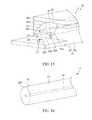
- FIG. 13 illustrates a perspective view of an optical communication apparatus 1 b according to an embodiment of the present disclosure.
- the optical communication apparatus 1 b is similar to the optical communication apparatus 1 a as shown in FIG. 12 , with a difference being that the optical communication apparatus 1 b further includes an adhesive 87 and a top cover 88 .
- the adhesive 87 is used to fill the recess portion 81 and cover the portion of the optical fiber structure 2 above the light source 12 .
- the top cover 88 contacts and is pressed onto the adhesive 87 to fix the optical fiber structure 2 in position.
- FIG. 14 illustrates a perspective view of an optical communication apparatus 1 c according to an embodiment of the present disclosure.
- the optical communication apparatus 1 c is similar to the optical communication apparatus 1 as shown in FIG. 1-3 , with a difference being that the optical communication apparatus 1 c further includes a substrate 8 a for receiving the optical fiber structure 2 and the light source 12 .
- the substrate 8 a includes a first portion 85 and a second portion 86 .
- the first portion 85 extends horizontally from the second portion 86 at a bottom of the second portion 86 .
- the second portion 86 defines a groove 861 .
- the light source 12 is disposed on the first portion 85 , and the optical fiber structure 2 is disposed and fixed in the groove 861 so that the light incident surface 222 faces the light source 12 .
- FIG. 15 illustrates a perspective view of an optical communication apparatus 1 d according to an embodiment of the present disclosure.
- the optical communication apparatus 1 d is similar to the optical communication apparatus 1 c as shown in FIG. 14 , with a difference being that the optical communication apparatus 1 d further includes an adhesive 87 a and a top cover 88 a .
- the adhesive 87 a is used to fill the groove 861 and cover the portion of the optical fiber structure 2 in and above the groove 861 .
- the top cover 88 a contacts and is pressed onto the adhesive 87 a to fix the optical fiber structure 2 in position.
- FIGS. 16-19 illustrate a manufacturing process according to an embodiment of the present disclosure.
- the fiber 9 includes a core portion 20 , a cladding portion 22 an end portion 91 .
- the cladding portion 22 encloses/surrounds the core portion 20 , and a refractive index of the cladding portion 22 is lower than a refractive index of the core portion 20 .
- the core portion 20 and the cladding portion 22 may include a same or similar materials.
- the core portion 20 and the cladding portion 22 include silica (e.g., SiO 2 ).
- the cladding portion 22 has an end surface 228 at the end portion 91 of the fiber 9 .
- the end surface 228 is perpendicular to a line along which the core portion 20 lies.
- the fiber 9 is a single mode fiber, a diameter of the cladding portion 22 is approximately 125 ⁇ m, and a diameter of the core portion 20 is approximately 8 ⁇ m.
- a portion of the end portion 91 of the fiber 9 is removed (e.g., by grinding or etching), to form a light reflection surface 221 inclined at an angle ⁇ with respect to the core portion 20 .
- the angle ⁇ is about 30 degrees to about 60 degrees, such as about 35 degrees to about 55 degrees, about 40 degrees to about 50 degrees, or about 45 degrees.
- One end 201 of the core portion 20 is exposed from the light reflection surface 221 .
- a portion of a periphery of the fiber 9 is removed (e.g., by grinding or etching), to form a light incident surface 222 .
- a portion of the light reflection surface 221 is also removed; thus, the light reflection surface 221 and the light incident surface 222 intersect to form a wedge portion 224 and an intersecting edge 225 , and the optical fiber structure 2 as illustrated and described with respect to FIGS. 1-3 is obtained.
- the cladding portion 22 has a notch 223 on a bottom portion thereof, and the light incident surface 222 is a top surface of the notch 223 .
- the portion of the light reflection surface 221 is not removed (e.g., a notch 223 ′ is made narrower than the notch 223 , or is shifted away from the light incident surface 222 ); thus, the light reflection surface 221 does not intersect with the light incident surface 222 , and the optical fiber structure 3 as illustrated and described with respect to FIG. 4 is obtained.
- a grating structure may be formed on the light incident surface 222 .
- a grating structure with periodic protrusions may be formed, such as periodic columnar structures with approximately square cross-section as shown in FIGS. 5 and 6 , or such as periodic U-shaped structures with three differently-sized portions as shown in FIG. 8 .
- the grating structure may be formed, for example, by coating a material on the light incident surface 222 , by etching the light incident surface 222 , or a combination thereof.
- protrusions e.g., the protrusions 51 in FIGS.
- protrusions are formed of TiO 2 , which has a refractive index similar to a refractive index of the cladding portion 22 (e.g., SiO 2 ), for constructive interference when a light beam passes through the grating structure into the cladding portion 22 .
- the protrusions and the cladding portion 22 are formed of the same material.
- protrusions are formed by etching the light incident surface 222 , and then coating a material onto the light incident surface 222 along the sides of the protrusions.
- a reflection film of one or more layers is formed on the light reflection surface 221 (e.g., the reflection film 61 , to obtain the optical fiber structure 6 of FIG. 9 ).
- the reflection film may be formed by coating.
- the reflection film includes Au.
- an anti-reflection film of one or more layers is formed on the light incident surface 222 (e.g., the reflection film 70 , to obtain the optical fiber structure 7 of FIG. 10 ).
- the anti-reflection film includes a layer of SiO 2 formed over the light incident surface 222 and a layer of TiO 2 formed over the layer of SiO 2 .
- one or more additional layers are formed over the layer of TiO 2 .
- the reflection film includes four layers (a first layer over the light incident surface 222 , a second layer over the first layer, a third layer over the second layer, and a fourth layer over the third layer), where a refractive index of the third layer is less than a refractive index of the second layer and may be approximately equal to a refractive index of the first layer, and a refractive index of the fourth layer is greater than the refractive index of the third layer and may be approximately equal to the refractive index of the second layer.
- the substrate 8 includes a recess portion 81 , a side wall 82 , a bottom wall 83 and a groove 84 .
- the recess portion 81 is defined by the side wall 82 and the bottom wall 83 , and the groove 84 is located on a top side of the side wall 82 .
- a light source 12 is disposed on the bottom wall 83 in the recess portion 81 .
- the light source 12 is a VCSEL light source or an edge-emitting laser light source.
- the optical fiber structure 2 is disposed in and fixed in the groove 84 on the side wall 82 transversely, so that the light incident surface 222 faces the light source 12 .
- the optical communication apparatus 1 a as shown in FIG. 12 is obtained.
- an adhesive 87 ( FIG. 13 ) and a top cover 88 are further provided.
- the adhesive 87 is used to fill the recess portion 81 and cover the portion of the optical fiber structure 2 above the light source 12 .
- the top cover 88 contacts and is pressed onto the adhesive 87 to fix the optical fiber structure 2 in position.
- the optical communication apparatus 1 b as shown in FIG. 13 is obtained.
- FIG. 20 illustrates a manufacturing process according to an embodiment of the present disclosure.
- the initial stages of this embodiment are as shown in FIGS. 16 to 18 , and the stage of FIG. 20 is subsequent to the stage of FIG. 18 .
- a substrate 8 a is provided.
- the substrate 8 a includes a first portion 85 and a second portion 86 .
- the first portion 85 extends horizontally from a bottom of the second portion 86 .
- the second portion 86 defines a groove 861 .
- a light source 12 is disposed on the first portion 85 .
- the light source 12 is a VCSEL light source or an edge-emitting laser light source.
- the optical fiber structure 2 is disposed in and fixed in the groove 861 so that the light incident surface 222 faces the light source 12 .
- the optical communication apparatus 1 b as shown in FIG. 13 is obtained.
- an adhesive 87 a ( FIG. 15 ) and a top cover 88 a are further provided.
- the adhesive 87 a is used to fill the groove 861 and cover the portion of the optical fiber structure 2 in and above the groove 861 .
- the top cover 88 a contacts and is pressed onto the adhesive 87 a to fix the optical fiber structure 2 in position.
- the optical communication apparatus 1 d as shown in FIG. 15 is obtained.
- an optical communication apparatus may omit a rotatable micromirror; thus, manufacturing cost is reduced.
- the terms “substantially,” “substantial,” “approximately” and “about” are used to describe and account for small variations. When used in conjunction with an event or circumstance, the terms can encompass instances in which the event or circumstance occurs precisely as well as instances in which the event or circumstance occurs to a close approximation.
- the terms when used in conjunction with a numerical value, can encompass a range of variation of less than or equal to ⁇ 10% of that numerical value, such as less than or equal to ⁇ 5%, less than or equal to ⁇ 4%, less than or equal to ⁇ 3%, less than or equal to ⁇ 2%, less than or equal to ⁇ 1%, less than or equal to ⁇ 0.5%, less than or equal to ⁇ 0.1%, or less than or equal to ⁇ 0.05%.
- two numerical values can be deemed to be substantially the same if a difference between the values is less than or equal to ⁇ 10% of an average of the values, such as less than or equal to ⁇ 5%, less than or equal to ⁇ 4%, less than or equal to ⁇ 3%, less than or equal to ⁇ 2%, less than or equal to ⁇ 1%, less than or equal to ⁇ 0.5%, less than or equal to ⁇ 0.1%, or less than or equal to ⁇ 0.05%.
- substantially perpendicular referring to two components can refer to a range of variation of less than or equal to ⁇ 10° of 90° between the two components, such as less than or equal to ⁇ 5°, less than or equal to ⁇ 3°, less than or equal to ⁇ 2°, or less than or equal to ⁇ 1°.
- substantially parallel referring to two components (each component laying along one of a line or a plane) can refer to an angular displacement between the two components being less than or equal to 10°, such as less than or equal to 5°, less than or equal to 3°, less than or equal to 2°, or less than or equal to 1°.
- substantially flat can refer to a surface where a difference between a highest point and a lowest point of the surface is no greater than 3 ⁇ m, no greater than 2 ⁇ m, no greater than 1 ⁇ m, no greater than 0.5 ⁇ m, or no greater than 0.1 ⁇ m.
Landscapes
- Physics & Mathematics (AREA)
- General Physics & Mathematics (AREA)
- Optics & Photonics (AREA)
- Optical Couplings Of Light Guides (AREA)
Abstract
Description
Claims (18)
Priority Applications (2)
| Application Number | Priority Date | Filing Date | Title |
|---|---|---|---|
| US15/057,936 US10025033B2 (en) | 2016-03-01 | 2016-03-01 | Optical fiber structure, optical communication apparatus and manufacturing process for manufacturing the same |
| CN201710034688.9A CN107144925B (en) | 2016-03-01 | 2017-01-18 | Optical fiber structures, optical communication devices and manufacturing processes for their manufacture |
Applications Claiming Priority (1)
| Application Number | Priority Date | Filing Date | Title |
|---|---|---|---|
| US15/057,936 US10025033B2 (en) | 2016-03-01 | 2016-03-01 | Optical fiber structure, optical communication apparatus and manufacturing process for manufacturing the same |
Publications (2)
| Publication Number | Publication Date |
|---|---|
| US20170254956A1 US20170254956A1 (en) | 2017-09-07 |
| US10025033B2 true US10025033B2 (en) | 2018-07-17 |
Family
ID=59723561
Family Applications (1)
| Application Number | Title | Priority Date | Filing Date |
|---|---|---|---|
| US15/057,936 Active US10025033B2 (en) | 2016-03-01 | 2016-03-01 | Optical fiber structure, optical communication apparatus and manufacturing process for manufacturing the same |
Country Status (2)
| Country | Link |
|---|---|
| US (1) | US10025033B2 (en) |
| CN (1) | CN107144925B (en) |
Cited By (3)
| Publication number | Priority date | Publication date | Assignee | Title |
|---|---|---|---|---|
| US20180231783A1 (en) * | 2017-02-16 | 2018-08-16 | Coretronic Corporation | Optical waveguide element and display device |
| US20190196114A1 (en) * | 2016-06-24 | 2019-06-27 | Senko Advanced Components (Hong Kong) Limited | A Parallel Optical Fiber Angled Coupling Component |
| US10558044B2 (en) | 2016-03-30 | 2020-02-11 | Coretronic Corporation | Optical waveguide device and head-mounted display apparatus using the same |
Families Citing this family (2)
| Publication number | Priority date | Publication date | Assignee | Title |
|---|---|---|---|---|
| GB202019741D0 (en) * | 2020-12-15 | 2021-01-27 | Ams Sensors Singapore Pte Ltd | Illumination Module |
| US20250180839A1 (en) * | 2023-12-01 | 2025-06-05 | Shenzhen 8k Link Optoelectronics Technology Co., Ltd. | Mult-chip package design module of glass v-groove design without conventional wire bonding |
Citations (193)
| Publication number | Priority date | Publication date | Assignee | Title |
|---|---|---|---|---|
| US4351585A (en) * | 1978-11-29 | 1982-09-28 | Siemens Aktiengesellschaft | Coupling element for an optical waveguide |
| US5598495A (en) | 1992-11-13 | 1997-01-28 | International Business Machines Corporation | Fiber optic connector housing, fiber optic receptacle, accessories employing fiber optic connector housings and corresponding optical assemblies |
| US5684905A (en) * | 1995-06-12 | 1997-11-04 | Hamamatsu Phototnics K.K. | Fiber optic plate for making pattern image incident on photosensor |
| US6088153A (en) | 1997-06-26 | 2000-07-11 | Scientific-Atlanta, Inc. | Multi-functional optical isolator |
| US6229158B1 (en) | 1999-05-25 | 2001-05-08 | Intel Corporation | Stacked die integrated circuit device |
| US6229712B1 (en) | 1999-03-31 | 2001-05-08 | International Business Machines Corporation | Printed circuit board for coupling surface mounted optoelectric semiconductor devices |
| US6253005B1 (en) | 1999-06-10 | 2001-06-26 | Agere Systems Optoelectronics Guardian Corp. | Apparatus and method for compensating for misalignment in reflective packages |
| US6275625B1 (en) | 1999-03-17 | 2001-08-14 | Agere Systems Optoelectronics Guardian Corp. | Optical mirror switch using a michelson interferometer |
| US6325552B1 (en) | 2000-02-14 | 2001-12-04 | Cisco Technology, Inc. | Solderless optical transceiver interconnect |
| US6351329B1 (en) | 1999-10-08 | 2002-02-26 | Lucent Technologies Inc. | Optical attenuator |
| US6363203B1 (en) | 1999-09-16 | 2002-03-26 | Agere Systems Guardian Corp. | Variable fiber optic attenuator |
| US6370311B1 (en) | 2000-04-17 | 2002-04-09 | Lucent Technologies Inc. | Hermetic optical fiber arrays and methods for making same |
| US6374012B1 (en) | 1999-09-30 | 2002-04-16 | Agere Systems Guardian Corp. | Method and apparatus for adjusting the path of an optical beam |
| US6388798B2 (en) | 1999-10-29 | 2002-05-14 | Intel Corporation | Integrated circuit with opposed spatial light modulator and processor |
| US6396711B1 (en) | 2000-06-06 | 2002-05-28 | Agere Systems Guardian Corp. | Interconnecting micromechanical devices |
| US6399418B1 (en) | 2001-07-26 | 2002-06-04 | Amkor Technology, Inc. | Method for forming a reduced thickness packaged electronic device |
| US6404533B1 (en) | 2000-09-09 | 2002-06-11 | International Business Machines Corporation | Optical amplitude modulator |
| US6408120B1 (en) | 1999-10-20 | 2002-06-18 | Agere Systems Guardian Corp. | Fiber array alignment arrangement |
| US6411757B1 (en) | 2000-02-14 | 2002-06-25 | Agere Systems Guardian Corp. | Article comprising a waveguide structure with improved pump utilization |
| US6420204B2 (en) | 1999-06-03 | 2002-07-16 | Amkor Technology, Inc. | Method of making a plastic package for an optical integrated circuit device |
| US6431765B1 (en) | 1999-06-11 | 2002-08-13 | Cisco Technology Inc. | Distributed network repeater module and method |
| US20020114260A1 (en) * | 2001-02-16 | 2002-08-22 | Nobuyuki Kasama | Information recording/reproduction apparatus |
| US6442307B1 (en) | 2000-11-03 | 2002-08-27 | Lucent Technologies Inc. | Solder-packaged optical MEMs device and method for making the same |
| US6439895B1 (en) | 2001-09-10 | 2002-08-27 | Intel Corporation | Pin-free socket compatible with optical/electrical interconnects |
| US6442306B1 (en) | 1999-12-21 | 2002-08-27 | Agere Systems Guardian Corp. | Self-aligned fiber optic connector for NxM arrays |
| US6448506B1 (en) | 2000-12-28 | 2002-09-10 | Amkor Technology, Inc. | Semiconductor package and circuit board for making the package |
| US6477301B1 (en) | 1997-06-26 | 2002-11-05 | Scientific-Atlanta, Inc. | Micro-optic coupler incorporating a tapered fiber |
| US6487001B2 (en) | 2000-12-13 | 2002-11-26 | Agere Systems Inc. | Article comprising wedge-shaped electrodes |
| US6487356B1 (en) | 2000-07-31 | 2002-11-26 | Cisco Technology, Inc. | Fiber optic cable segregation and slack storage apparatus and method |
| US6512861B2 (en) | 2001-06-26 | 2003-01-28 | Intel Corporation | Packaging and assembly method for optical coupling |
| US6519075B2 (en) | 2000-11-03 | 2003-02-11 | Agere Systems Inc. | Packaged MEMS device and method for making the same |
| US6560377B2 (en) | 2001-10-01 | 2003-05-06 | Agere Systems Inc. | Non-hermetic packaging for lithium niobate-based devices |
| US6564454B1 (en) | 2000-12-28 | 2003-05-20 | Amkor Technology, Inc. | Method of making and stacking a semiconductor package |
| US6576998B1 (en) | 2002-02-28 | 2003-06-10 | Amkor Technology, Inc. | Thin semiconductor package with semiconductor chip and electronic discrete device |
| US6586824B1 (en) | 2001-07-26 | 2003-07-01 | Amkor Technology, Inc. | Reduced thickness packaged electronic device |
| US6603183B1 (en) | 2001-09-04 | 2003-08-05 | Amkor Technology, Inc. | Quick sealing glass-lidded package |
| US6618184B2 (en) | 2001-04-03 | 2003-09-09 | Agere Systems Inc. | Device for use with a micro-electro-mechanical system (MEMS) optical device and a method of manufacture therefor |
| US6624444B1 (en) | 2002-03-28 | 2003-09-23 | Intel Corporation | Electrical-optical package with capacitor DC shunts and associated methods |
| US6628452B2 (en) | 2000-09-15 | 2003-09-30 | International Business Machines Corporation | Optical devices |
| US6630661B1 (en) | 2001-12-12 | 2003-10-07 | Amkor Technology, Inc. | Sensor module with integrated discrete components mounted on a window |
| US6639724B2 (en) | 2001-06-05 | 2003-10-28 | Lucent Technologies Inc. | Device having a barrier layer located therein and a method of manufacture therefor |
| US6646290B1 (en) | 2002-08-23 | 2003-11-11 | Amkor Technology, Inc. | Optical structure having an optical diode and a sensor in separate apertures inside double insulating layers |
| US6661943B2 (en) | 2002-01-30 | 2003-12-09 | Intel Corporation | Fiber-free optical interconnect system for chip-to-chip signaling |
| US6686588B1 (en) | 2001-01-16 | 2004-02-03 | Amkor Technology, Inc. | Optical module with lens integral holder |
| US6702476B2 (en) | 2002-05-02 | 2004-03-09 | Agere Systems Inc. | Optical fiber device having attachment to optical device package |
| US6704476B2 (en) | 2001-06-29 | 2004-03-09 | Lucent Technologies Inc. | Optical MEMS switch with imaging system |
| US6704475B2 (en) | 2001-04-03 | 2004-03-09 | Agere Systems Inc. | Mirror for use with a micro-electro-mechanical system (MEMS) optical device and a method of manufacture therefor |
| US6712527B1 (en) | 2000-01-12 | 2004-03-30 | International Business Machines Corporation | Fiber optic connections and method for using same |
| US6718086B1 (en) | 2000-02-10 | 2004-04-06 | Agere Systems, Inc. | Article comprising a tunable filter |
| US6716657B1 (en) | 2000-05-26 | 2004-04-06 | Agere Systems Inc | Method for interconnecting arrays of micromechanical devices |
| US6740950B2 (en) | 2001-01-15 | 2004-05-25 | Amkor Technology, Inc. | Optical device packages having improved conductor efficiency, optical coupling and thermal transfer |
| US6748125B2 (en) | 2001-05-17 | 2004-06-08 | Sioptical, Inc. | Electronic semiconductor control of light in optical waveguide |
| US20040114859A1 (en) * | 2002-12-17 | 2004-06-17 | International Business Machines Corporation | Devices and methods for side-coupling optical fibers to optoelectronic components |
| US6754407B2 (en) | 2001-06-26 | 2004-06-22 | Intel Corporation | Flip-chip package integrating optical and electrical devices and coupling to a waveguide on a board |
| US6757458B2 (en) | 2001-06-29 | 2004-06-29 | Lucent Technologies Inc. | Optical MEMS switch with converging beams |
| US6759266B1 (en) | 2001-09-04 | 2004-07-06 | Amkor Technology, Inc. | Quick sealing glass-lidded package fabrication method |
| US6765801B1 (en) | 2001-06-25 | 2004-07-20 | Amkor Technology, Inc. | Optical track drain package |
| US6771850B1 (en) | 2000-11-18 | 2004-08-03 | Agere Systems Inc. | Article comprising a MEMS device and method therefor |
| US20040156590A1 (en) | 2003-02-11 | 2004-08-12 | Luxtera, Inc. | Optical waveguide grating coupler |
| US6784534B1 (en) | 2002-02-06 | 2004-08-31 | Amkor Technology, Inc. | Thin integrated circuit package having an optically transparent window |
| US6788847B2 (en) | 2001-04-05 | 2004-09-07 | Luxtera, Inc. | Photonic input/output port |
| US6792178B1 (en) | 2000-01-12 | 2004-09-14 | Finisar Corporation | Fiber optic header with integrated power monitor |
| US6793407B2 (en) | 2002-09-25 | 2004-09-21 | International Business Machines Corporation | Manufacturable optical connection assemblies |
| US6801676B1 (en) | 2003-06-24 | 2004-10-05 | Intel Corporation | Method and apparatus for phase shifting an optical beam in an optical device with a buffer plug |
| US6807218B1 (en) | 2002-05-13 | 2004-10-19 | Amkor Technology, Inc. | Laser module and optical subassembly |
| US6809258B1 (en) | 2003-02-24 | 2004-10-26 | Cisco Technology, Inc. | Apparatus for cable routing management |
| US6809848B2 (en) | 2001-06-01 | 2004-10-26 | Agere Systems Inc. | MEMS device |
| US6813054B2 (en) | 2002-03-21 | 2004-11-02 | Agere Systems Inc. | Micro-electro-mechanical device having improved torsional members and a method of manufacturing therefor |
| US6819813B2 (en) | 2002-09-11 | 2004-11-16 | International Business Machines Corporation | Optical land grid array interposer |
| US6836185B1 (en) | 2002-05-17 | 2004-12-28 | Inphi Corp. | High-speed electro-optical modulator drivers and method |
| US6839517B2 (en) | 2001-02-12 | 2005-01-04 | Agere Systems Inc. | Apparatus and method for transmitting optical signals through a single fiber optical network |
| US6846087B2 (en) | 2002-07-30 | 2005-01-25 | Lucent Technologies Inc. | Micromirror having counterbalancing structures and method for manufacturing same |
| US6856730B2 (en) | 2002-07-22 | 2005-02-15 | Intel Corporation | Athermal package for fiber Bragg gratings with two or more bonding regions |
| US6859324B2 (en) | 2002-07-31 | 2005-02-22 | Agere Systems Inc. | Optical demultiplexer/multiplexer architecture |
| US6861720B1 (en) | 2001-08-29 | 2005-03-01 | Amkor Technology, Inc. | Placement template and method for placing optical dies |
| US6864553B2 (en) | 2002-07-30 | 2005-03-08 | Intel Corporation | Method and apparatus for a backsided and recessed optical package connection |
| US6869815B2 (en) | 2002-08-22 | 2005-03-22 | Agere Systems Inc. | Electro-mechanical device having a charge dissipation layer and a method of manufacture therefor |
| US6879751B2 (en) | 2002-01-30 | 2005-04-12 | Sioptical, Inc. | Method and apparatus for altering the effective mode index of an optical waveguide |
| US6891685B2 (en) | 2001-05-17 | 2005-05-10 | Sioptical, Inc. | Anisotropic etching of optical components |
| US6896422B2 (en) | 2003-02-04 | 2005-05-24 | Intel Corporation | Optoelectronic modules and methods of manufacturing the same |
| US20050117833A1 (en) * | 2003-11-27 | 2005-06-02 | International Business Machines Corporation | Optical transmission substrate, method for manufacturing optical transmission substrate and optoelectronic integrated circuit |
| US6906846B2 (en) | 2002-08-14 | 2005-06-14 | Triquint Technology Holding Co. | Micro-electro-mechanical system device and method of making same |
| US6912330B2 (en) | 2001-05-17 | 2005-06-28 | Sioptical Inc. | Integrated optical/electronic circuits and associated methods of simultaneous generation thereof |
| US6922499B2 (en) | 2001-07-24 | 2005-07-26 | Lucent Technologies Inc. | MEMS driver circuit arrangement |
| US6944008B2 (en) | 2002-12-18 | 2005-09-13 | Lucent Technologies Inc. | Charge dissipation in electrostatically driven devices |
| US6955481B2 (en) | 2003-09-17 | 2005-10-18 | International Business Machines Corporation | Method and apparatus for providing parallel optoelectronic communication with an electronic device |
| US6968110B2 (en) | 2003-04-21 | 2005-11-22 | Sioptical, Inc. | CMOS-compatible integration of silicon-based optical devices with electronic devices |
| US6973230B1 (en) | 1999-05-27 | 2005-12-06 | Cisco Technology Inc. | Distributed network repeater system |
| US6975784B1 (en) | 2004-09-10 | 2005-12-13 | Intel Corporation | Singulated dies in a parallel optics module |
| US6975664B1 (en) | 1999-08-30 | 2005-12-13 | Agere Systems Inc. | Article comprising a two-dimensional photonic crystal coupler and method of making the same |
| US7000434B2 (en) | 2000-12-19 | 2006-02-21 | Intel Corporation | Method of creating an angled waveguide using lithographic techniques |
| US7003196B2 (en) | 2003-09-04 | 2006-02-21 | Sioptical, Inc. | External grating structures for interfacing wavelength-division-multiplexed optical sources with thin optical waveguides |
| US7013067B2 (en) | 2004-02-11 | 2006-03-14 | Sioptical, Inc. | Silicon nanotaper couplers and mode-matching devices |
| US7020364B2 (en) | 2003-03-31 | 2006-03-28 | Sioptical Inc. | Permanent light coupling arrangement and method for use with thin silicon optical waveguides |
| US7026707B2 (en) | 1998-10-13 | 2006-04-11 | Intel Corporation | Windowed package having embedded frame |
| US7039263B2 (en) | 2002-09-24 | 2006-05-02 | Intel Corporation | Electrooptic assembly |
| US7042106B2 (en) | 2003-06-24 | 2006-05-09 | Intel Corporation | Underfill integration for optical packages |
| US7054534B1 (en) | 2002-06-24 | 2006-05-30 | Luxtera, Inc | Light scattering structures formed in silicon strip loaded waveguides |
| US7058247B2 (en) | 2003-12-17 | 2006-06-06 | International Business Machines Corporation | Silicon carrier for optical interconnect modules |
| US7059040B1 (en) | 2001-01-16 | 2006-06-13 | Amkor Technology, Inc. | Optical module with lens integral holder fabrication method |
| US20060127003A1 (en) * | 2004-12-10 | 2006-06-15 | Park Kang H | Optical fiber illuminator, method of fabricating the optical fiber illuminator, and optical recording head and optical recording and reading apparatus having the optical fiber illuminator |
| US7068892B1 (en) | 2005-03-29 | 2006-06-27 | Intel Corporation | Passively aligned optical-electrical interface |
| US20060140553A1 (en) | 2004-05-17 | 2006-06-29 | Cisco Technology, Inc. | Multiple channel optical tranceiver modules with compatibility features |
| US7081981B2 (en) | 2004-03-31 | 2006-07-25 | Intel Corporation | Thermally tuned filter having a pre-stressed membrane |
| US7095620B2 (en) | 2002-11-27 | 2006-08-22 | International Business Machines Corp. | Optically connectable circuit board with optical component(s) mounted thereon |
| US7123798B2 (en) * | 2002-03-29 | 2006-10-17 | Ngk Insulators, Ltd. | Optical device and method of producing the same |
| US7125176B1 (en) * | 2003-09-30 | 2006-10-24 | Stafford John W | PCB with embedded optical fiber |
| US7146106B2 (en) | 2002-08-23 | 2006-12-05 | Amkor Technology, Inc. | Optic semiconductor module and manufacturing method |
| US7159421B2 (en) | 2002-07-16 | 2007-01-09 | Agere Systems Inc. | Manufacture of planar waveguides using sol-gel techniques |
| US7162124B1 (en) * | 2003-03-14 | 2007-01-09 | Luxtera, Inc. | Fiber to chip coupler |
| US7177499B2 (en) | 2003-03-28 | 2007-02-13 | Intel Corporation | Athermal package for fiber bragg gratings with compensation for non-linear thermal response |
| US7187837B2 (en) | 2004-02-26 | 2007-03-06 | Sioptical, Inc. | Active manipulation of light in a silicon-on-insulator (SOI) structure |
| US7194166B1 (en) | 2004-08-26 | 2007-03-20 | Luxtera, Inc. | Use of waveguide grating couplers in an optical mux/demux system |
| US7224076B2 (en) | 2002-10-08 | 2007-05-29 | Agere Systems Inc | Electronic component package |
| US7229221B2 (en) | 2005-06-20 | 2007-06-12 | Intel Corporation | Optical transponder with passive heat transfer |
| US7260293B1 (en) | 2003-02-11 | 2007-08-21 | Luxtera, Inc. | Optical waveguide grating coupler with varying scatter cross sections |
| US7283699B2 (en) | 2004-09-30 | 2007-10-16 | Intel Corporation | Optical package |
| US7298939B1 (en) | 2003-04-07 | 2007-11-20 | Luxtera, Inc. | Optoelectronic alignment structures for the wafer level testing of optical and optoelectronic chips |
| US7334946B2 (en) | 2005-12-21 | 2008-02-26 | Intel Corporation | Passively aligned optical-electrical interface with microlenses |
| US7343058B2 (en) | 2003-04-22 | 2008-03-11 | Intel Corporation | Efficient light coupler from off-chip to on-chip waveguides |
| US7352066B2 (en) | 2003-09-30 | 2008-04-01 | International Business Machines Corporation | Silicon based optical vias |
| US7359591B2 (en) | 2001-12-19 | 2008-04-15 | Intel Corporation | Electrical/optical integration scheme using direct copper bonding |
| US7359609B2 (en) | 2005-06-14 | 2008-04-15 | Scientific-Atlanta, Inc. | Storage trough and fiber management system |
| US7369718B2 (en) | 2004-01-23 | 2008-05-06 | Intel Corporation | Package substrate pattern to accommodate optical waveguide |
| US7367715B1 (en) | 2007-03-22 | 2008-05-06 | International Business Machines Corporation | Medium containing optical paths and electrically conducting paths for applications in high speed data links |
| US7373044B2 (en) | 2003-04-18 | 2008-05-13 | International Business Machines Corporation | Optical link module, optical interconnection method, information processor including the optical link module, signal transfer method, prism and method of manufacturing the prism |
| US7373033B2 (en) | 2006-06-13 | 2008-05-13 | Intel Corporation | Chip-to-chip optical interconnect |
| US7415184B2 (en) | 2006-01-11 | 2008-08-19 | Sioptical Inc. | Wideband optical coupling into thin SOI CMOS photonic integrated circuit |
| US7433193B2 (en) | 2005-05-11 | 2008-10-07 | Cisco Technology, Inc. | Techniques for controlling a position of a transceiver module relative to a connector |
| US7453132B1 (en) | 2002-06-19 | 2008-11-18 | Luxtera Inc. | Waveguide photodetector with integrated electronics |
| US7470069B1 (en) | 2008-03-20 | 2008-12-30 | International Business Machines Corporation | Optoelectronic MCM package |
| US7477811B1 (en) | 2008-03-25 | 2009-01-13 | International Business Machines Corporation | Method of forming a three-dimensional stacked optical device |
| US7480426B1 (en) | 2008-03-25 | 2009-01-20 | International Business Machines Corporation | Method of forming a three-dimensional stacked optical device |
| US7486847B1 (en) | 2008-03-31 | 2009-02-03 | International Business Machines Corporation | Chip carrier package with optical vias |
| US7539366B1 (en) | 2008-01-04 | 2009-05-26 | International Business Machines Corporation | Optical transceiver module |
| US7556440B2 (en) | 2006-12-22 | 2009-07-07 | Lightwire Inc. | Dual-lensed unitary optical receiver assembly |
| US7576401B1 (en) | 2005-07-07 | 2009-08-18 | Amkor Technology, Inc. | Direct glass attached on die optical module |
| US20090214156A1 (en) * | 2008-02-21 | 2009-08-27 | Sony Corporation | Optical module and optical waveguide |
| US7630601B2 (en) | 2003-09-22 | 2009-12-08 | Intel Corporation | Connecting a component with an embedded optical fiber |
| US20100008675A1 (en) | 2005-12-14 | 2010-01-14 | Luxtera, Inc. | Integrated transceiver with lightpipe coupler |
| US7676132B1 (en) | 2002-08-06 | 2010-03-09 | Cisco Technology, Inc. | Bend radius control |
| US7684660B2 (en) | 2005-06-24 | 2010-03-23 | Intel Corporation | Methods and apparatus to mount a waveguide to a substrate |
| US7701985B2 (en) | 2007-11-09 | 2010-04-20 | Lightwire, Inc. | SOI-based tunable laser |
| US20100129038A1 (en) * | 2008-11-21 | 2010-05-27 | Fuji Xerox Co., Ltd. | Optical transmission apparatus |
| US7826692B2 (en) | 2006-11-13 | 2010-11-02 | Samtec, Inc. | Connector assembly |
| US7853105B2 (en) | 2007-04-10 | 2010-12-14 | International Business Machines Corporation | Coupling element alignment using waveguide fiducials |
| US7936033B2 (en) | 2008-12-29 | 2011-05-03 | Texas Instruments Incorporated | Micro-optical device packaging system |
| US7941023B2 (en) | 2004-12-21 | 2011-05-10 | Lightwire Inc. | Ultra low-loss CMOS compatible silicon waveguides |
| US7945127B2 (en) | 2007-09-19 | 2011-05-17 | Intel Corporation | Electrically pluggable optical interconnect |
| US20110127633A1 (en) | 2009-12-01 | 2011-06-02 | Lightwire, Inc. | Slotted Configuration for Optimized Placement of Micro-Components using Adhesive Bonding |
| US20110216997A1 (en) | 2003-04-23 | 2011-09-08 | Lightwire, Inc. | Sub-Micron Planar Lightwave Devices Formed on an SOI Optical Platform |
| US8057108B2 (en) | 2003-02-03 | 2011-11-15 | Intel Corporation | Method and apparatus to generate and monitor optical signals and control power levels thereof in a planar lightwave circuit |
| US20110317958A1 (en) | 2010-06-29 | 2011-12-29 | Lightwire, Inc. | Vent Structures For Encapsulated Components On An SOI-Based Photonics Platform |
| US8200056B2 (en) | 2008-10-16 | 2012-06-12 | Lightwire LLC | Multi-fiber interface to photonic subassembly |
| US8231284B2 (en) | 2007-03-26 | 2012-07-31 | International Business Machines Corporation | Ultra-high bandwidth, multiple-channel full-duplex, single-chip CMOS optical transceiver |
| US8265432B2 (en) | 2008-03-10 | 2012-09-11 | International Business Machines Corporation | Optical transceiver module with optical windows |
| US8280207B2 (en) | 2008-11-06 | 2012-10-02 | Luxtera Inc. | Method and system for coupling optical signals into silicon optoelectronic chips |
| US20120289034A1 (en) | 2010-08-31 | 2012-11-15 | Micron Technology, Inc. | Methods of Forming NAND Memory Constructions |
| US20130022316A1 (en) * | 2011-07-19 | 2013-01-24 | Teraxion Inc. | Fiber Coupling Technique on a Waveguide |
| US8373259B2 (en) | 2010-07-27 | 2013-02-12 | Intel Corporation | Optical connection through single assembly overhang flip chip optics die with micro structure alignment |
| US8488921B2 (en) | 2010-07-16 | 2013-07-16 | International Business Machines Corporation | Packaged multicore fiber optical transceiver module |
| US20130202255A1 (en) | 2012-02-01 | 2013-08-08 | Cisco Technology, Inc. | Single Mode Fiber Array Connector For Opto-Electronic Transceivers |
| US20130243368A1 (en) | 2012-03-14 | 2013-09-19 | Mellanox Technologies Ltd. | Optoelectronic interconnects using l-shaped fixture |
| US8545108B1 (en) | 2012-03-23 | 2013-10-01 | International Business Machines Corporation | Flexible fiber to wafer interface |
| US8588561B2 (en) | 2011-07-01 | 2013-11-19 | Samtec, Inc. | Transceiver and interface for IC package |
| US20130315528A1 (en) | 2012-05-28 | 2013-11-28 | Mellanox Technologies Ltd. | High-speed optical module with flexible printed circuit board |
| US8613561B2 (en) | 2007-03-30 | 2013-12-24 | Intel Corporation | Optical universal serial bus (USB) |
| US8626002B2 (en) | 2009-07-10 | 2014-01-07 | Luxtera, Inc. | Method and system for optoelectronic receivers for uncoded data |
| US8694721B2 (en) | 2011-04-11 | 2014-04-08 | Inphi Corporation | Memory buffer with one or more auxiliary interfaces |
| US8724937B2 (en) | 2011-12-20 | 2014-05-13 | International Business Machines Corporation | Fiber to wafer interface |
| US8731346B2 (en) | 2012-06-28 | 2014-05-20 | Intel Corporation | Waveguide integration on laser for alignment-tolerant assembly |
| US8750657B2 (en) | 2012-11-15 | 2014-06-10 | Mellanox Technologies Ltd. | Flip-chip optical interface with micro-lens array |
| US8755644B2 (en) | 2003-09-30 | 2014-06-17 | International Business Machines Corporation | Silicon based optical vias |
| US20140169789A1 (en) | 2012-09-11 | 2014-06-19 | Inphi Corporation | Optical communication interface utilizing coded pulse amplitude modulation |
| US8831437B2 (en) | 2009-09-04 | 2014-09-09 | Luxtera, Inc. | Method and system for a photonic interposer |
| US20140269804A1 (en) | 2013-03-12 | 2014-09-18 | Taiwan Semiconductor Manufacturing Company, Ltd. | Package Structure and Methods of Forming Same |
| US20140284463A1 (en) | 2011-10-31 | 2014-09-25 | Yamaichi Electronics Co., Ltd. | Optical module |
| US20140306131A1 (en) | 2008-07-09 | 2014-10-16 | Luxtera, Inc. | Light source assembly supporting direct coupling to an integrated circuit |
| US8873912B2 (en) | 2009-04-08 | 2014-10-28 | International Business Machines Corporation | Optical waveguide with embedded light-reflecting feature and method for fabricating the same |
| US8873899B2 (en) | 2013-03-14 | 2014-10-28 | Cisco Technology, Inc. | Modal rotation in optical waveguides |
| US8871570B2 (en) | 2012-03-14 | 2014-10-28 | Mellanox Technologies Ltd. | Method of fabricating integrated optoelectronic interconnects with side mounted transducer |
| US8876410B2 (en) | 2012-01-11 | 2014-11-04 | Cisco Technology, Inc. | Self-aligning connectorized fiber array assembly |
| US8905632B2 (en) | 2011-11-29 | 2014-12-09 | Cisco Technology, Inc. | Interposer configuration with thermally isolated regions for temperature-sensitive opto-electronic components |
| US20140369651A1 (en) | 2013-06-13 | 2014-12-18 | Mellanox Technologies Ltd. | Integrated optical cooling core for optoelectronic interconnect modules |
| US8923664B2 (en) | 2010-06-15 | 2014-12-30 | Luxtera, Inc. | Method and system for multi-mode integrated receivers |
| US8926196B2 (en) | 2012-09-28 | 2015-01-06 | Intel Corporation | Method and apparatus for an optical interconnect system |
| US20150010268A1 (en) | 2013-07-04 | 2015-01-08 | Mellanox Technologies Ltd. | Polymer-based interconnection between silicon photonics devices and optical fibers |
| US20150023452A1 (en) | 2012-09-11 | 2015-01-22 | Inphi Corporation | Optical communication interface utilizing n-dimensional double square quadrature amplitude modulation |
| US20150021291A1 (en) | 2013-07-18 | 2015-01-22 | Cisco Technology, Inc. | Coupling system for optical fibers and optical waveguides |
| US8944704B2 (en) | 2013-05-21 | 2015-02-03 | Mellanox Technologies Ltd. | Transceiver socket adapter for passive optical cable |
| US20150037029A1 (en) | 2013-08-04 | 2015-02-05 | Mellanox Technologies Ltd. | Wavelength auto-negotiation |
| US8983291B1 (en) | 2012-07-30 | 2015-03-17 | Inphi Corporation | Optical PAM modulation with dual drive mach zehnder modulators and low complexity electrical signaling |
| US20150110501A1 (en) | 2012-09-27 | 2015-04-23 | Inphi Corporation | Direct-coupled driver for mach-zehnder optical modulators |
-
2016
- 2016-03-01 US US15/057,936 patent/US10025033B2/en active Active
-
2017
- 2017-01-18 CN CN201710034688.9A patent/CN107144925B/en active Active
Patent Citations (233)
| Publication number | Priority date | Publication date | Assignee | Title |
|---|---|---|---|---|
| US4351585A (en) * | 1978-11-29 | 1982-09-28 | Siemens Aktiengesellschaft | Coupling element for an optical waveguide |
| US5598495A (en) | 1992-11-13 | 1997-01-28 | International Business Machines Corporation | Fiber optic connector housing, fiber optic receptacle, accessories employing fiber optic connector housings and corresponding optical assemblies |
| US5684905A (en) * | 1995-06-12 | 1997-11-04 | Hamamatsu Phototnics K.K. | Fiber optic plate for making pattern image incident on photosensor |
| US6088153A (en) | 1997-06-26 | 2000-07-11 | Scientific-Atlanta, Inc. | Multi-functional optical isolator |
| US6477301B1 (en) | 1997-06-26 | 2002-11-05 | Scientific-Atlanta, Inc. | Micro-optic coupler incorporating a tapered fiber |
| US7026707B2 (en) | 1998-10-13 | 2006-04-11 | Intel Corporation | Windowed package having embedded frame |
| US6275625B1 (en) | 1999-03-17 | 2001-08-14 | Agere Systems Optoelectronics Guardian Corp. | Optical mirror switch using a michelson interferometer |
| US6229712B1 (en) | 1999-03-31 | 2001-05-08 | International Business Machines Corporation | Printed circuit board for coupling surface mounted optoelectric semiconductor devices |
| US6229158B1 (en) | 1999-05-25 | 2001-05-08 | Intel Corporation | Stacked die integrated circuit device |
| US6973230B1 (en) | 1999-05-27 | 2005-12-06 | Cisco Technology Inc. | Distributed network repeater system |
| US6420204B2 (en) | 1999-06-03 | 2002-07-16 | Amkor Technology, Inc. | Method of making a plastic package for an optical integrated circuit device |
| US6253005B1 (en) | 1999-06-10 | 2001-06-26 | Agere Systems Optoelectronics Guardian Corp. | Apparatus and method for compensating for misalignment in reflective packages |
| US6431765B1 (en) | 1999-06-11 | 2002-08-13 | Cisco Technology Inc. | Distributed network repeater module and method |
| US6975664B1 (en) | 1999-08-30 | 2005-12-13 | Agere Systems Inc. | Article comprising a two-dimensional photonic crystal coupler and method of making the same |
| US6363203B1 (en) | 1999-09-16 | 2002-03-26 | Agere Systems Guardian Corp. | Variable fiber optic attenuator |
| US6374012B1 (en) | 1999-09-30 | 2002-04-16 | Agere Systems Guardian Corp. | Method and apparatus for adjusting the path of an optical beam |
| US6351329B1 (en) | 1999-10-08 | 2002-02-26 | Lucent Technologies Inc. | Optical attenuator |
| US6408120B1 (en) | 1999-10-20 | 2002-06-18 | Agere Systems Guardian Corp. | Fiber array alignment arrangement |
| US6388798B2 (en) | 1999-10-29 | 2002-05-14 | Intel Corporation | Integrated circuit with opposed spatial light modulator and processor |
| US6442306B1 (en) | 1999-12-21 | 2002-08-27 | Agere Systems Guardian Corp. | Self-aligned fiber optic connector for NxM arrays |
| US6792178B1 (en) | 2000-01-12 | 2004-09-14 | Finisar Corporation | Fiber optic header with integrated power monitor |
| US6712527B1 (en) | 2000-01-12 | 2004-03-30 | International Business Machines Corporation | Fiber optic connections and method for using same |
| US6718086B1 (en) | 2000-02-10 | 2004-04-06 | Agere Systems, Inc. | Article comprising a tunable filter |
| US6411757B1 (en) | 2000-02-14 | 2002-06-25 | Agere Systems Guardian Corp. | Article comprising a waveguide structure with improved pump utilization |
| US6325552B1 (en) | 2000-02-14 | 2001-12-04 | Cisco Technology, Inc. | Solderless optical transceiver interconnect |
| US6370311B1 (en) | 2000-04-17 | 2002-04-09 | Lucent Technologies Inc. | Hermetic optical fiber arrays and methods for making same |
| US6716657B1 (en) | 2000-05-26 | 2004-04-06 | Agere Systems Inc | Method for interconnecting arrays of micromechanical devices |
| US6396711B1 (en) | 2000-06-06 | 2002-05-28 | Agere Systems Guardian Corp. | Interconnecting micromechanical devices |
| US6487356B1 (en) | 2000-07-31 | 2002-11-26 | Cisco Technology, Inc. | Fiber optic cable segregation and slack storage apparatus and method |
| US6404533B1 (en) | 2000-09-09 | 2002-06-11 | International Business Machines Corporation | Optical amplitude modulator |
| US6628452B2 (en) | 2000-09-15 | 2003-09-30 | International Business Machines Corporation | Optical devices |
| US6442307B1 (en) | 2000-11-03 | 2002-08-27 | Lucent Technologies Inc. | Solder-packaged optical MEMs device and method for making the same |
| US6519075B2 (en) | 2000-11-03 | 2003-02-11 | Agere Systems Inc. | Packaged MEMS device and method for making the same |
| US6771850B1 (en) | 2000-11-18 | 2004-08-03 | Agere Systems Inc. | Article comprising a MEMS device and method therefor |
| US6487001B2 (en) | 2000-12-13 | 2002-11-26 | Agere Systems Inc. | Article comprising wedge-shaped electrodes |
| US7000434B2 (en) | 2000-12-19 | 2006-02-21 | Intel Corporation | Method of creating an angled waveguide using lithographic techniques |
| US6448506B1 (en) | 2000-12-28 | 2002-09-10 | Amkor Technology, Inc. | Semiconductor package and circuit board for making the package |
| US6564454B1 (en) | 2000-12-28 | 2003-05-20 | Amkor Technology, Inc. | Method of making and stacking a semiconductor package |
| US6740950B2 (en) | 2001-01-15 | 2004-05-25 | Amkor Technology, Inc. | Optical device packages having improved conductor efficiency, optical coupling and thermal transfer |
| US7609461B1 (en) | 2001-01-16 | 2009-10-27 | Amkor Technology, Inc. | Optical module having cavity substrate |
| US6686588B1 (en) | 2001-01-16 | 2004-02-03 | Amkor Technology, Inc. | Optical module with lens integral holder |
| US7059040B1 (en) | 2001-01-16 | 2006-06-13 | Amkor Technology, Inc. | Optical module with lens integral holder fabrication method |
| US6839517B2 (en) | 2001-02-12 | 2005-01-04 | Agere Systems Inc. | Apparatus and method for transmitting optical signals through a single fiber optical network |
| US20020114260A1 (en) * | 2001-02-16 | 2002-08-22 | Nobuyuki Kasama | Information recording/reproduction apparatus |
| US6618184B2 (en) | 2001-04-03 | 2003-09-09 | Agere Systems Inc. | Device for use with a micro-electro-mechanical system (MEMS) optical device and a method of manufacture therefor |
| US6704475B2 (en) | 2001-04-03 | 2004-03-09 | Agere Systems Inc. | Mirror for use with a micro-electro-mechanical system (MEMS) optical device and a method of manufacture therefor |
| US7031562B2 (en) | 2001-04-05 | 2006-04-18 | Luxtera, Inc. | Photonic input/output port |
| US7269326B2 (en) | 2001-04-05 | 2007-09-11 | Luxtera, Inc. | Photonic input/output port |
| US6788847B2 (en) | 2001-04-05 | 2004-09-07 | Luxtera, Inc. | Photonic input/output port |
| US7409327B2 (en) | 2001-05-17 | 2008-08-05 | Sioptical Inc. | Simulation program for integrated optical/electronic circuit |
| US6748125B2 (en) | 2001-05-17 | 2004-06-08 | Sioptical, Inc. | Electronic semiconductor control of light in optical waveguide |
| US6912330B2 (en) | 2001-05-17 | 2005-06-28 | Sioptical Inc. | Integrated optical/electronic circuits and associated methods of simultaneous generation thereof |
| US6944369B2 (en) | 2001-05-17 | 2005-09-13 | Sioptical, Inc. | Optical coupler having evanescent coupling region |
| US6891685B2 (en) | 2001-05-17 | 2005-05-10 | Sioptical, Inc. | Anisotropic etching of optical components |
| US6809848B2 (en) | 2001-06-01 | 2004-10-26 | Agere Systems Inc. | MEMS device |
| US6639724B2 (en) | 2001-06-05 | 2003-10-28 | Lucent Technologies Inc. | Device having a barrier layer located therein and a method of manufacture therefor |
| US6765801B1 (en) | 2001-06-25 | 2004-07-20 | Amkor Technology, Inc. | Optical track drain package |
| US6754407B2 (en) | 2001-06-26 | 2004-06-22 | Intel Corporation | Flip-chip package integrating optical and electrical devices and coupling to a waveguide on a board |
| US7049704B2 (en) | 2001-06-26 | 2006-05-23 | Intel Corporation | Flip-chip package integrating optical and electrical devices and coupling to a waveguide on a board |
| US6512861B2 (en) | 2001-06-26 | 2003-01-28 | Intel Corporation | Packaging and assembly method for optical coupling |
| US6704476B2 (en) | 2001-06-29 | 2004-03-09 | Lucent Technologies Inc. | Optical MEMS switch with imaging system |
| US6757458B2 (en) | 2001-06-29 | 2004-06-29 | Lucent Technologies Inc. | Optical MEMS switch with converging beams |
| US6922499B2 (en) | 2001-07-24 | 2005-07-26 | Lucent Technologies Inc. | MEMS driver circuit arrangement |
| US6586824B1 (en) | 2001-07-26 | 2003-07-01 | Amkor Technology, Inc. | Reduced thickness packaged electronic device |
| US6399418B1 (en) | 2001-07-26 | 2002-06-04 | Amkor Technology, Inc. | Method for forming a reduced thickness packaged electronic device |
| US6861720B1 (en) | 2001-08-29 | 2005-03-01 | Amkor Technology, Inc. | Placement template and method for placing optical dies |
| US6759266B1 (en) | 2001-09-04 | 2004-07-06 | Amkor Technology, Inc. | Quick sealing glass-lidded package fabrication method |
| US6603183B1 (en) | 2001-09-04 | 2003-08-05 | Amkor Technology, Inc. | Quick sealing glass-lidded package |
| US6439895B1 (en) | 2001-09-10 | 2002-08-27 | Intel Corporation | Pin-free socket compatible with optical/electrical interconnects |
| US6560377B2 (en) | 2001-10-01 | 2003-05-06 | Agere Systems Inc. | Non-hermetic packaging for lithium niobate-based devices |
| US6630661B1 (en) | 2001-12-12 | 2003-10-07 | Amkor Technology, Inc. | Sensor module with integrated discrete components mounted on a window |
| US7359591B2 (en) | 2001-12-19 | 2008-04-15 | Intel Corporation | Electrical/optical integration scheme using direct copper bonding |
| US7826694B2 (en) | 2001-12-19 | 2010-11-02 | Intel Corporation | Electrical/optical integration scheme using direct copper bonding |
| US6661943B2 (en) | 2002-01-30 | 2003-12-09 | Intel Corporation | Fiber-free optical interconnect system for chip-to-chip signaling |
| US6879751B2 (en) | 2002-01-30 | 2005-04-12 | Sioptical, Inc. | Method and apparatus for altering the effective mode index of an optical waveguide |
| US6784534B1 (en) | 2002-02-06 | 2004-08-31 | Amkor Technology, Inc. | Thin integrated circuit package having an optically transparent window |
| US6576998B1 (en) | 2002-02-28 | 2003-06-10 | Amkor Technology, Inc. | Thin semiconductor package with semiconductor chip and electronic discrete device |
| US6813054B2 (en) | 2002-03-21 | 2004-11-02 | Agere Systems Inc. | Micro-electro-mechanical device having improved torsional members and a method of manufacturing therefor |
| US6841842B2 (en) | 2002-03-28 | 2005-01-11 | Intel Corporation | Method and apparatus for electrical-optical packaging with capacitive DC shunts |
| US6624444B1 (en) | 2002-03-28 | 2003-09-23 | Intel Corporation | Electrical-optical package with capacitor DC shunts and associated methods |
| US7123798B2 (en) * | 2002-03-29 | 2006-10-17 | Ngk Insulators, Ltd. | Optical device and method of producing the same |
| US6702476B2 (en) | 2002-05-02 | 2004-03-09 | Agere Systems Inc. | Optical fiber device having attachment to optical device package |
| US6807218B1 (en) | 2002-05-13 | 2004-10-19 | Amkor Technology, Inc. | Laser module and optical subassembly |
| US6836185B1 (en) | 2002-05-17 | 2004-12-28 | Inphi Corp. | High-speed electro-optical modulator drivers and method |
| US7616904B1 (en) | 2002-06-19 | 2009-11-10 | Luxtera, Inc. | Waveguide photodetector with integrated electronics |
| US7453132B1 (en) | 2002-06-19 | 2008-11-18 | Luxtera Inc. | Waveguide photodetector with integrated electronics |
| US7054534B1 (en) | 2002-06-24 | 2006-05-30 | Luxtera, Inc | Light scattering structures formed in silicon strip loaded waveguides |
| US7082246B1 (en) | 2002-06-24 | 2006-07-25 | Luxtera, Inc. | Light scattering structures formed in lower layer of strip loaded waveguides |
| US7116881B1 (en) | 2002-06-24 | 2006-10-03 | Luxtera, Inc. | CMOS process polysilicon strip loaded waveguides with a three layer core |
| US7159421B2 (en) | 2002-07-16 | 2007-01-09 | Agere Systems Inc. | Manufacture of planar waveguides using sol-gel techniques |
| US6856730B2 (en) | 2002-07-22 | 2005-02-15 | Intel Corporation | Athermal package for fiber Bragg gratings with two or more bonding regions |
| US6864553B2 (en) | 2002-07-30 | 2005-03-08 | Intel Corporation | Method and apparatus for a backsided and recessed optical package connection |
| US6846087B2 (en) | 2002-07-30 | 2005-01-25 | Lucent Technologies Inc. | Micromirror having counterbalancing structures and method for manufacturing same |
| US6859324B2 (en) | 2002-07-31 | 2005-02-22 | Agere Systems Inc. | Optical demultiplexer/multiplexer architecture |
| US7676132B1 (en) | 2002-08-06 | 2010-03-09 | Cisco Technology, Inc. | Bend radius control |
| US6906846B2 (en) | 2002-08-14 | 2005-06-14 | Triquint Technology Holding Co. | Micro-electro-mechanical system device and method of making same |
| US6869815B2 (en) | 2002-08-22 | 2005-03-22 | Agere Systems Inc. | Electro-mechanical device having a charge dissipation layer and a method of manufacture therefor |
| US7015056B2 (en) | 2002-08-22 | 2006-03-21 | Agere Systems Inc. | Electro-mechanical device having a charge dissipation layer and a method of manufacture therefor |
| US7146106B2 (en) | 2002-08-23 | 2006-12-05 | Amkor Technology, Inc. | Optic semiconductor module and manufacturing method |
| US6646290B1 (en) | 2002-08-23 | 2003-11-11 | Amkor Technology, Inc. | Optical structure having an optical diode and a sensor in separate apertures inside double insulating layers |
| US6819813B2 (en) | 2002-09-11 | 2004-11-16 | International Business Machines Corporation | Optical land grid array interposer |
| US7039263B2 (en) | 2002-09-24 | 2006-05-02 | Intel Corporation | Electrooptic assembly |
| US6793407B2 (en) | 2002-09-25 | 2004-09-21 | International Business Machines Corporation | Manufacturable optical connection assemblies |
| US8913856B2 (en) | 2002-09-25 | 2014-12-16 | International Business Machines Corporation | Manufacturable optical connection assemblies |
| US7224076B2 (en) | 2002-10-08 | 2007-05-29 | Agere Systems Inc | Electronic component package |
| US7539376B2 (en) | 2002-11-27 | 2009-05-26 | International Business Machines Corporation | Optically connectable circuit board with optical component(s) mounted thereon |
| US7095620B2 (en) | 2002-11-27 | 2006-08-22 | International Business Machines Corp. | Optically connectable circuit board with optical component(s) mounted thereon |
| US7551453B2 (en) | 2002-11-27 | 2009-06-23 | International Business Machines Corporation | Optically connectable circuit board with optical component(s) mounted thereon |
| US20040114859A1 (en) * | 2002-12-17 | 2004-06-17 | International Business Machines Corporation | Devices and methods for side-coupling optical fibers to optoelectronic components |
| US6944008B2 (en) | 2002-12-18 | 2005-09-13 | Lucent Technologies Inc. | Charge dissipation in electrostatically driven devices |
| US8057108B2 (en) | 2003-02-03 | 2011-11-15 | Intel Corporation | Method and apparatus to generate and monitor optical signals and control power levels thereof in a planar lightwave circuit |
| US6896422B2 (en) | 2003-02-04 | 2005-05-24 | Intel Corporation | Optoelectronic modules and methods of manufacturing the same |
| US20040156590A1 (en) | 2003-02-11 | 2004-08-12 | Luxtera, Inc. | Optical waveguide grating coupler |
| US7260289B1 (en) | 2003-02-11 | 2007-08-21 | Luxtera, Inc. | Optical waveguide grating coupler with varying scatter cross sections |
| US7260293B1 (en) | 2003-02-11 | 2007-08-21 | Luxtera, Inc. | Optical waveguide grating coupler with varying scatter cross sections |
| US7245803B2 (en) | 2003-02-11 | 2007-07-17 | Luxtera, Inc. | Optical waveguide grating coupler |
| US6809258B1 (en) | 2003-02-24 | 2004-10-26 | Cisco Technology, Inc. | Apparatus for cable routing management |
| US7162124B1 (en) * | 2003-03-14 | 2007-01-09 | Luxtera, Inc. | Fiber to chip coupler |
| US7177499B2 (en) | 2003-03-28 | 2007-02-13 | Intel Corporation | Athermal package for fiber bragg gratings with compensation for non-linear thermal response |
| US7020364B2 (en) | 2003-03-31 | 2006-03-28 | Sioptical Inc. | Permanent light coupling arrangement and method for use with thin silicon optical waveguides |
| US7298939B1 (en) | 2003-04-07 | 2007-11-20 | Luxtera, Inc. | Optoelectronic alignment structures for the wafer level testing of optical and optoelectronic chips |
| US7412138B1 (en) | 2003-04-07 | 2008-08-12 | Luxtera, Inc. | Optoelectronic alignment structures for the wafer level testing of optical and optoelectronic chips |
| US7373044B2 (en) | 2003-04-18 | 2008-05-13 | International Business Machines Corporation | Optical link module, optical interconnection method, information processor including the optical link module, signal transfer method, prism and method of manufacturing the prism |
| US7903911B2 (en) | 2003-04-18 | 2011-03-08 | International Business Machines Corporation | Optical link module, optical interconnection method, information processor including the optical link module, signal transfer method, prism and method of manufacturing the prism |
| US6968110B2 (en) | 2003-04-21 | 2005-11-22 | Sioptical, Inc. | CMOS-compatible integration of silicon-based optical devices with electronic devices |
| US7343058B2 (en) | 2003-04-22 | 2008-03-11 | Intel Corporation | Efficient light coupler from off-chip to on-chip waveguides |
| US7801397B2 (en) | 2003-04-22 | 2010-09-21 | Intel Corporation | Efficient light coupler from off-chip to on-chip waveguides |
| US20110216997A1 (en) | 2003-04-23 | 2011-09-08 | Lightwire, Inc. | Sub-Micron Planar Lightwave Devices Formed on an SOI Optical Platform |
| US7042106B2 (en) | 2003-06-24 | 2006-05-09 | Intel Corporation | Underfill integration for optical packages |
| US7256059B2 (en) | 2003-06-24 | 2007-08-14 | Intel Corporation | Underfill integration for optical packages |
| US6801676B1 (en) | 2003-06-24 | 2004-10-05 | Intel Corporation | Method and apparatus for phase shifting an optical beam in an optical device with a buffer plug |
| US7003196B2 (en) | 2003-09-04 | 2006-02-21 | Sioptical, Inc. | External grating structures for interfacing wavelength-division-multiplexed optical sources with thin optical waveguides |
| US6955481B2 (en) | 2003-09-17 | 2005-10-18 | International Business Machines Corporation | Method and apparatus for providing parallel optoelectronic communication with an electronic device |
| US7630601B2 (en) | 2003-09-22 | 2009-12-08 | Intel Corporation | Connecting a component with an embedded optical fiber |
| US7352066B2 (en) | 2003-09-30 | 2008-04-01 | International Business Machines Corporation | Silicon based optical vias |
| US7125176B1 (en) * | 2003-09-30 | 2006-10-24 | Stafford John W | PCB with embedded optical fiber |
| US8755644B2 (en) | 2003-09-30 | 2014-06-17 | International Business Machines Corporation | Silicon based optical vias |
| US7212713B2 (en) | 2003-11-27 | 2007-05-01 | International Business Machines Corporation | Optical transmission substrate, method for manufacturing optical transmission substrate and optoelectronic integrated circuit |
| US20050117833A1 (en) * | 2003-11-27 | 2005-06-02 | International Business Machines Corporation | Optical transmission substrate, method for manufacturing optical transmission substrate and optoelectronic integrated circuit |
| US7058247B2 (en) | 2003-12-17 | 2006-06-06 | International Business Machines Corporation | Silicon carrier for optical interconnect modules |
| USRE45215E1 (en) | 2004-01-14 | 2014-10-28 | Luxtera, Inc. | Integrated transceiver with lightpipe coupler |
| US8577191B2 (en) | 2004-01-14 | 2013-11-05 | Luxtera Inc. | Low-cost transceiver approach |
| USRE45214E1 (en) | 2004-01-14 | 2014-10-28 | Luxtera, Inc. | Integrated transceiver with lightpipe coupler |
| USRE45390E1 (en) | 2004-01-14 | 2015-02-24 | Luxtera, Inc. | Integrated transceiver with lightpipe coupler |
| US7369718B2 (en) | 2004-01-23 | 2008-05-06 | Intel Corporation | Package substrate pattern to accommodate optical waveguide |
| US7013067B2 (en) | 2004-02-11 | 2006-03-14 | Sioptical, Inc. | Silicon nanotaper couplers and mode-matching devices |
| US7187837B2 (en) | 2004-02-26 | 2007-03-06 | Sioptical, Inc. | Active manipulation of light in a silicon-on-insulator (SOI) structure |
| US7081981B2 (en) | 2004-03-31 | 2006-07-25 | Intel Corporation | Thermally tuned filter having a pre-stressed membrane |
| US7731432B2 (en) | 2004-05-17 | 2010-06-08 | Cisco Technology, Inc. | Multiple channel optical transceiver modules with compatibility features |
| US20060140553A1 (en) | 2004-05-17 | 2006-06-29 | Cisco Technology, Inc. | Multiple channel optical tranceiver modules with compatibility features |
| US7194166B1 (en) | 2004-08-26 | 2007-03-20 | Luxtera, Inc. | Use of waveguide grating couplers in an optical mux/demux system |
| US7333695B2 (en) | 2004-09-10 | 2008-02-19 | Intel Corporation | Singulated dies in a parallel optics module |
| US6975784B1 (en) | 2004-09-10 | 2005-12-13 | Intel Corporation | Singulated dies in a parallel optics module |
| US7095914B2 (en) | 2004-09-10 | 2006-08-22 | Intel Corporation | Singulated dies in a parallel optics module |
| US7283699B2 (en) | 2004-09-30 | 2007-10-16 | Intel Corporation | Optical package |
| US20060127003A1 (en) * | 2004-12-10 | 2006-06-15 | Park Kang H | Optical fiber illuminator, method of fabricating the optical fiber illuminator, and optical recording head and optical recording and reading apparatus having the optical fiber illuminator |
| US7941023B2 (en) | 2004-12-21 | 2011-05-10 | Lightwire Inc. | Ultra low-loss CMOS compatible silicon waveguides |
| US7068892B1 (en) | 2005-03-29 | 2006-06-27 | Intel Corporation | Passively aligned optical-electrical interface |
| US7433193B2 (en) | 2005-05-11 | 2008-10-07 | Cisco Technology, Inc. | Techniques for controlling a position of a transceiver module relative to a connector |
| US7359609B2 (en) | 2005-06-14 | 2008-04-15 | Scientific-Atlanta, Inc. | Storage trough and fiber management system |
| US7229221B2 (en) | 2005-06-20 | 2007-06-12 | Intel Corporation | Optical transponder with passive heat transfer |
| US7684660B2 (en) | 2005-06-24 | 2010-03-23 | Intel Corporation | Methods and apparatus to mount a waveguide to a substrate |
| US7911017B1 (en) | 2005-07-07 | 2011-03-22 | Amkor Technology, Inc. | Direct glass attached on die optical module |
| US7576401B1 (en) | 2005-07-07 | 2009-08-18 | Amkor Technology, Inc. | Direct glass attached on die optical module |
| US7961992B2 (en) | 2005-12-14 | 2011-06-14 | Luxtera, Inc. | Integrated transceiver with lightpipe coupler |
| US8165431B2 (en) | 2005-12-14 | 2012-04-24 | Luxtera, Inc. | Integrated transceiver with lightpipe coupler |
| US7773836B2 (en) | 2005-12-14 | 2010-08-10 | Luxtera, Inc. | Integrated transceiver with lightpipe coupler |
| US20100008675A1 (en) | 2005-12-14 | 2010-01-14 | Luxtera, Inc. | Integrated transceiver with lightpipe coupler |
| US7334946B2 (en) | 2005-12-21 | 2008-02-26 | Intel Corporation | Passively aligned optical-electrical interface with microlenses |
| US7415184B2 (en) | 2006-01-11 | 2008-08-19 | Sioptical Inc. | Wideband optical coupling into thin SOI CMOS photonic integrated circuit |
| US7373033B2 (en) | 2006-06-13 | 2008-05-13 | Intel Corporation | Chip-to-chip optical interconnect |
| US7826692B2 (en) | 2006-11-13 | 2010-11-02 | Samtec, Inc. | Connector assembly |
| US7556440B2 (en) | 2006-12-22 | 2009-07-07 | Lightwire Inc. | Dual-lensed unitary optical receiver assembly |
| US7367715B1 (en) | 2007-03-22 | 2008-05-06 | International Business Machines Corporation | Medium containing optical paths and electrically conducting paths for applications in high speed data links |
| US8231284B2 (en) | 2007-03-26 | 2012-07-31 | International Business Machines Corporation | Ultra-high bandwidth, multiple-channel full-duplex, single-chip CMOS optical transceiver |
| US8613561B2 (en) | 2007-03-30 | 2013-12-24 | Intel Corporation | Optical universal serial bus (USB) |
| US7853105B2 (en) | 2007-04-10 | 2010-12-14 | International Business Machines Corporation | Coupling element alignment using waveguide fiducials |
| US7945127B2 (en) | 2007-09-19 | 2011-05-17 | Intel Corporation | Electrically pluggable optical interconnect |
| US7701985B2 (en) | 2007-11-09 | 2010-04-20 | Lightwire, Inc. | SOI-based tunable laser |
| US7539366B1 (en) | 2008-01-04 | 2009-05-26 | International Business Machines Corporation | Optical transceiver module |
| US20090214156A1 (en) * | 2008-02-21 | 2009-08-27 | Sony Corporation | Optical module and optical waveguide |
| US8265432B2 (en) | 2008-03-10 | 2012-09-11 | International Business Machines Corporation | Optical transceiver module with optical windows |
| US7470069B1 (en) | 2008-03-20 | 2008-12-30 | International Business Machines Corporation | Optoelectronic MCM package |
| US7480426B1 (en) | 2008-03-25 | 2009-01-20 | International Business Machines Corporation | Method of forming a three-dimensional stacked optical device |
| US7477811B1 (en) | 2008-03-25 | 2009-01-13 | International Business Machines Corporation | Method of forming a three-dimensional stacked optical device |
| US7486847B1 (en) | 2008-03-31 | 2009-02-03 | International Business Machines Corporation | Chip carrier package with optical vias |
| US20140306131A1 (en) | 2008-07-09 | 2014-10-16 | Luxtera, Inc. | Light source assembly supporting direct coupling to an integrated circuit |
| US20140369693A1 (en) | 2008-09-08 | 2014-12-18 | Luxtera, Inc. | Method and system for a photonic interposer |
| US8200056B2 (en) | 2008-10-16 | 2012-06-12 | Lightwire LLC | Multi-fiber interface to photonic subassembly |
| US8280207B2 (en) | 2008-11-06 | 2012-10-02 | Luxtera Inc. | Method and system for coupling optical signals into silicon optoelectronic chips |
| US8861906B2 (en) | 2008-11-06 | 2014-10-14 | Luxtera, Inc. | Method and system for coupling optical signals into silicon optoelectronic chips |
| US20100129038A1 (en) * | 2008-11-21 | 2010-05-27 | Fuji Xerox Co., Ltd. | Optical transmission apparatus |
| US8445984B2 (en) | 2008-12-29 | 2013-05-21 | Texas Instruments Incorporated | Micro-optical device packaging system |
| US7936033B2 (en) | 2008-12-29 | 2011-05-03 | Texas Instruments Incorporated | Micro-optical device packaging system |
| US8873912B2 (en) | 2009-04-08 | 2014-10-28 | International Business Machines Corporation | Optical waveguide with embedded light-reflecting feature and method for fabricating the same |
| US8626002B2 (en) | 2009-07-10 | 2014-01-07 | Luxtera, Inc. | Method and system for optoelectronic receivers for uncoded data |
| US8831437B2 (en) | 2009-09-04 | 2014-09-09 | Luxtera, Inc. | Method and system for a photonic interposer |
| US20110127633A1 (en) | 2009-12-01 | 2011-06-02 | Lightwire, Inc. | Slotted Configuration for Optimized Placement of Micro-Components using Adhesive Bonding |
| US8923664B2 (en) | 2010-06-15 | 2014-12-30 | Luxtera, Inc. | Method and system for multi-mode integrated receivers |
| US20110317958A1 (en) | 2010-06-29 | 2011-12-29 | Lightwire, Inc. | Vent Structures For Encapsulated Components On An SOI-Based Photonics Platform |
| US8488921B2 (en) | 2010-07-16 | 2013-07-16 | International Business Machines Corporation | Packaged multicore fiber optical transceiver module |
| US8373259B2 (en) | 2010-07-27 | 2013-02-12 | Intel Corporation | Optical connection through single assembly overhang flip chip optics die with micro structure alignment |
| US20120289034A1 (en) | 2010-08-31 | 2012-11-15 | Micron Technology, Inc. | Methods of Forming NAND Memory Constructions |
| US8694721B2 (en) | 2011-04-11 | 2014-04-08 | Inphi Corporation | Memory buffer with one or more auxiliary interfaces |
| US8990488B2 (en) | 2011-04-11 | 2015-03-24 | Inphi Corporation | Memory buffer with one or more auxiliary interfaces |
| US20140286646A1 (en) | 2011-07-01 | 2014-09-25 | Samtec, Inc. | Transceiver and interface for ic package |
| US8787711B2 (en) | 2011-07-01 | 2014-07-22 | Samtec, Inc. | Transceiver and interface for IC package |
| US8588561B2 (en) | 2011-07-01 | 2013-11-19 | Samtec, Inc. | Transceiver and interface for IC package |
| US20130022316A1 (en) * | 2011-07-19 | 2013-01-24 | Teraxion Inc. | Fiber Coupling Technique on a Waveguide |
| US20140284463A1 (en) | 2011-10-31 | 2014-09-25 | Yamaichi Electronics Co., Ltd. | Optical module |
| US8905632B2 (en) | 2011-11-29 | 2014-12-09 | Cisco Technology, Inc. | Interposer configuration with thermally isolated regions for temperature-sensitive opto-electronic components |
| US8724937B2 (en) | 2011-12-20 | 2014-05-13 | International Business Machines Corporation | Fiber to wafer interface |
| US8876410B2 (en) | 2012-01-11 | 2014-11-04 | Cisco Technology, Inc. | Self-aligning connectorized fiber array assembly |
| US20150016784A1 (en) | 2012-01-11 | 2015-01-15 | Cisco Technology, Inc. | Self-aligning connectorized fiber array assembly |
| US20130202255A1 (en) | 2012-02-01 | 2013-08-08 | Cisco Technology, Inc. | Single Mode Fiber Array Connector For Opto-Electronic Transceivers |
| US8871570B2 (en) | 2012-03-14 | 2014-10-28 | Mellanox Technologies Ltd. | Method of fabricating integrated optoelectronic interconnects with side mounted transducer |
| US20130243368A1 (en) | 2012-03-14 | 2013-09-19 | Mellanox Technologies Ltd. | Optoelectronic interconnects using l-shaped fixture |
| US8545108B1 (en) | 2012-03-23 | 2013-10-01 | International Business Machines Corporation | Flexible fiber to wafer interface |
| US20130315528A1 (en) | 2012-05-28 | 2013-11-28 | Mellanox Technologies Ltd. | High-speed optical module with flexible printed circuit board |
| US8731346B2 (en) | 2012-06-28 | 2014-05-20 | Intel Corporation | Waveguide integration on laser for alignment-tolerant assembly |
| US8983291B1 (en) | 2012-07-30 | 2015-03-17 | Inphi Corporation | Optical PAM modulation with dual drive mach zehnder modulators and low complexity electrical signaling |
| US20140169789A1 (en) | 2012-09-11 | 2014-06-19 | Inphi Corporation | Optical communication interface utilizing coded pulse amplitude modulation |
| US20150023452A1 (en) | 2012-09-11 | 2015-01-22 | Inphi Corporation | Optical communication interface utilizing n-dimensional double square quadrature amplitude modulation |
| US20150110501A1 (en) | 2012-09-27 | 2015-04-23 | Inphi Corporation | Direct-coupled driver for mach-zehnder optical modulators |
| US8926196B2 (en) | 2012-09-28 | 2015-01-06 | Intel Corporation | Method and apparatus for an optical interconnect system |
| US8750657B2 (en) | 2012-11-15 | 2014-06-10 | Mellanox Technologies Ltd. | Flip-chip optical interface with micro-lens array |
| US20140269804A1 (en) | 2013-03-12 | 2014-09-18 | Taiwan Semiconductor Manufacturing Company, Ltd. | Package Structure and Methods of Forming Same |
| US8873899B2 (en) | 2013-03-14 | 2014-10-28 | Cisco Technology, Inc. | Modal rotation in optical waveguides |
| US8944704B2 (en) | 2013-05-21 | 2015-02-03 | Mellanox Technologies Ltd. | Transceiver socket adapter for passive optical cable |
| US20140369651A1 (en) | 2013-06-13 | 2014-12-18 | Mellanox Technologies Ltd. | Integrated optical cooling core for optoelectronic interconnect modules |
| US20150010268A1 (en) | 2013-07-04 | 2015-01-08 | Mellanox Technologies Ltd. | Polymer-based interconnection between silicon photonics devices and optical fibers |
| US20150021291A1 (en) | 2013-07-18 | 2015-01-22 | Cisco Technology, Inc. | Coupling system for optical fibers and optical waveguides |
| US20150037029A1 (en) | 2013-08-04 | 2015-02-05 | Mellanox Technologies Ltd. | Wavelength auto-negotiation |
Cited By (5)
| Publication number | Priority date | Publication date | Assignee | Title |
|---|---|---|---|---|
| US10558044B2 (en) | 2016-03-30 | 2020-02-11 | Coretronic Corporation | Optical waveguide device and head-mounted display apparatus using the same |
| US20190196114A1 (en) * | 2016-06-24 | 2019-06-27 | Senko Advanced Components (Hong Kong) Limited | A Parallel Optical Fiber Angled Coupling Component |
| US11415755B2 (en) * | 2016-06-24 | 2022-08-16 | Senko Advanced Components, Inc. | Parallel optical fiber angled coupling component |
| US20180231783A1 (en) * | 2017-02-16 | 2018-08-16 | Coretronic Corporation | Optical waveguide element and display device |
| US10437068B2 (en) * | 2017-02-16 | 2019-10-08 | Coretronic Corporation | Optical waveguide element and display device |
Also Published As
| Publication number | Publication date |
|---|---|
| US20170254956A1 (en) | 2017-09-07 |
| CN107144925B (en) | 2020-01-17 |
| CN107144925A (en) | 2017-09-08 |
Similar Documents
| Publication | Publication Date | Title |
|---|---|---|
| US10025033B2 (en) | Optical fiber structure, optical communication apparatus and manufacturing process for manufacturing the same | |
| JP6122962B2 (en) | Optical connector | |
| US10992104B2 (en) | Dual layer grating coupler | |
| US10830951B2 (en) | Optical circuit and optical device | |
| US11747529B2 (en) | Wafer level microstructures for an optical lens | |
| US20180306952A1 (en) | Transmission grating and laser device using the same, and method of producing transmission grating | |
| CN106170898A (en) | Lasers with beam shape and beam direction modification | |
| US20130308906A1 (en) | System and method for dense coupling between optical devices and an optical fiber array | |
| US20240241296A1 (en) | Method for fabricating a blazed grating | |
| JP6359848B2 (en) | Optical receptacle and optical module having the same | |
| US10539815B2 (en) | Edge construction on optical devices | |
| CN1713468B (en) | Seal-capping for wafer-scale optoelectronic packages and preparation method thereof | |
| JP6161605B2 (en) | Optical receptacle and optical module having the same | |
| JP3834024B2 (en) | Optical waveguide component and manufacturing method thereof | |
| US10649147B2 (en) | Optical module | |
| CN117940813A (en) | Optoelectronic semiconductor devices and glasses | |
| CN103078251B (en) | Surface emitting laser and image forming apparatus | |
| JP3043718B2 (en) | Laser device and manufacturing method thereof | |
| US20240201426A1 (en) | Multi-layer high-efficiency dielectric grating with improved manufacturability | |
| JP4729893B2 (en) | Manufacturing method of semiconductor optical device | |
| JP2012059898A (en) | Semiconductor laser array | |
| US9134483B2 (en) | Optical coupling system having an optical coupler and a light-transmissive external medium and also production and use of such a system | |
| CN103901559A (en) | Optical coupling device | |
| JP2016018147A (en) | Optical circuit with mirror, and manufacturing method of optical circuit with mirror | |
| KR20210156457A (en) | Dielectric multilayer thin film diffraction grating without polarization dependence |
Legal Events
| Date | Code | Title | Description |
|---|---|---|---|
| AS | Assignment |
Owner name: ADVANCED SEMICONDUCTOR ENGINEERING, INC., TAIWAN Free format text: ASSIGNMENT OF ASSIGNORS INTEREST;ASSIGNORS:WANG, WEI LUN;CHIN, YI-MIN;LU, MEI-JU;AND OTHERS;REEL/FRAME:038449/0363 Effective date: 20160218 |
|
| STCF | Information on status: patent grant |
Free format text: PATENTED CASE |
|
| MAFP | Maintenance fee payment |
Free format text: PAYMENT OF MAINTENANCE FEE, 4TH YEAR, LARGE ENTITY (ORIGINAL EVENT CODE: M1551); ENTITY STATUS OF PATENT OWNER: LARGE ENTITY Year of fee payment: 4 |
|
| MAFP | Maintenance fee payment |
Free format text: PAYMENT OF MAINTENANCE FEE, 8TH YEAR, LARGE ENTITY (ORIGINAL EVENT CODE: M1552); ENTITY STATUS OF PATENT OWNER: LARGE ENTITY Year of fee payment: 8 |