US10018654B2 - Sensor circuit for detecting rotation of an object and method therefor - Google Patents
Sensor circuit for detecting rotation of an object and method therefor Download PDFInfo
- Publication number
- US10018654B2 US10018654B2 US14/533,742 US201414533742A US10018654B2 US 10018654 B2 US10018654 B2 US 10018654B2 US 201414533742 A US201414533742 A US 201414533742A US 10018654 B2 US10018654 B2 US 10018654B2
- Authority
- US
- United States
- Prior art keywords
- signal
- sensor
- mutual inductance
- receiver
- value
- Prior art date
- Legal status (The legal status is an assumption and is not a legal conclusion. Google has not performed a legal analysis and makes no representation as to the accuracy of the status listed.)
- Active, expires
Links
Images


Classifications
-
- G—PHYSICS
- G01—MEASURING; TESTING
- G01R—MEASURING ELECTRIC VARIABLES; MEASURING MAGNETIC VARIABLES
- G01R3/00—Apparatus or processes specially adapted for the manufacture or maintenance of measuring instruments, e.g. of probe tips
-
- G—PHYSICS
- G01—MEASURING; TESTING
- G01D—MEASURING NOT SPECIALLY ADAPTED FOR A SPECIFIC VARIABLE; ARRANGEMENTS FOR MEASURING TWO OR MORE VARIABLES NOT COVERED IN A SINGLE OTHER SUBCLASS; TARIFF METERING APPARATUS; MEASURING OR TESTING NOT OTHERWISE PROVIDED FOR
- G01D5/00—Mechanical means for transferring the output of a sensing member; Means for converting the output of a sensing member to another variable where the form or nature of the sensing member does not constrain the means for converting; Transducers not specially adapted for a specific variable
- G01D5/12—Mechanical means for transferring the output of a sensing member; Means for converting the output of a sensing member to another variable where the form or nature of the sensing member does not constrain the means for converting; Transducers not specially adapted for a specific variable using electric or magnetic means
- G01D5/14—Mechanical means for transferring the output of a sensing member; Means for converting the output of a sensing member to another variable where the form or nature of the sensing member does not constrain the means for converting; Transducers not specially adapted for a specific variable using electric or magnetic means influencing the magnitude of a current or voltage
- G01D5/20—Mechanical means for transferring the output of a sensing member; Means for converting the output of a sensing member to another variable where the form or nature of the sensing member does not constrain the means for converting; Transducers not specially adapted for a specific variable using electric or magnetic means influencing the magnitude of a current or voltage by varying inductance, e.g. by a movable armature
- G01D5/22—Mechanical means for transferring the output of a sensing member; Means for converting the output of a sensing member to another variable where the form or nature of the sensing member does not constrain the means for converting; Transducers not specially adapted for a specific variable using electric or magnetic means influencing the magnitude of a current or voltage by varying inductance, e.g. by a movable armature differentially influencing two coils
- G01D5/225—Mechanical means for transferring the output of a sensing member; Means for converting the output of a sensing member to another variable where the form or nature of the sensing member does not constrain the means for converting; Transducers not specially adapted for a specific variable using electric or magnetic means influencing the magnitude of a current or voltage by varying inductance, e.g. by a movable armature differentially influencing two coils by influencing the mutual induction between the two coils
- G01D5/2258—Mechanical means for transferring the output of a sensing member; Means for converting the output of a sensing member to another variable where the form or nature of the sensing member does not constrain the means for converting; Transducers not specially adapted for a specific variable using electric or magnetic means influencing the magnitude of a current or voltage by varying inductance, e.g. by a movable armature differentially influencing two coils by influencing the mutual induction between the two coils by a movable ferromagnetic element, e.g. core
- G01D5/2266—Mechanical means for transferring the output of a sensing member; Means for converting the output of a sensing member to another variable where the form or nature of the sensing member does not constrain the means for converting; Transducers not specially adapted for a specific variable using electric or magnetic means influencing the magnitude of a current or voltage by varying inductance, e.g. by a movable armature differentially influencing two coils by influencing the mutual induction between the two coils by a movable ferromagnetic element, e.g. core specially adapted circuits therefor
-
- G—PHYSICS
- G01—MEASURING; TESTING
- G01R—MEASURING ELECTRIC VARIABLES; MEASURING MAGNETIC VARIABLES
- G01R33/00—Arrangements or instruments for measuring magnetic variables
- G01R33/0017—Means for compensating offset magnetic fields or the magnetic flux to be measured; Means for generating calibration magnetic fields
-
- Y—GENERAL TAGGING OF NEW TECHNOLOGICAL DEVELOPMENTS; GENERAL TAGGING OF CROSS-SECTIONAL TECHNOLOGIES SPANNING OVER SEVERAL SECTIONS OF THE IPC; TECHNICAL SUBJECTS COVERED BY FORMER USPC CROSS-REFERENCE ART COLLECTIONS [XRACs] AND DIGESTS
- Y10—TECHNICAL SUBJECTS COVERED BY FORMER USPC
- Y10T—TECHNICAL SUBJECTS COVERED BY FORMER US CLASSIFICATION
- Y10T29/00—Metal working
- Y10T29/49—Method of mechanical manufacture
- Y10T29/49002—Electrical device making
- Y10T29/49117—Conductor or circuit manufacturing
Definitions
- the present invention relates, in general, to electronics, and more particularly, to semiconductors, structures thereof, and methods of forming semiconductor devices.
- the electronics industry various methods and structures to form position sensors.
- a Hall Effect sensor was used to sense the position.
- the sensor and the sensor interface could was implemented in an IC packaged with a permanent magnet. The IC could have been connected on a PCB with few extra devices.
- the cost of the sensor was higher than desired.
- the cost of the permanent magnet could be higher than was desired.
- electro-magnetic interference or noise from external to sensor could interfere with proper operation of the sensors.
- FIG. 1 illustrates one example of an embodiment of a portion of a rotational system that includes a proximity sensor system and movable object in accordance with the present invention
- FIG. 2 schematically illustrates an example of an embodiment of a portion of sensing system that may be an embodiment of a portion of the system FIG. 1 in accordance with the present invention
- FIG. 3 graphically illustrates some examples of embodiments of a portion of a combination of sensor elements that may be an example of alternate embodiments for the sensor elements of FIG. 2 in accordance with the present invention
- FIG. 4 graphically illustrates a portion of an example of an embodiment of some configurations of the sensor elements FIG. 1 in accordance with the present invention
- FIG. 5 schematically illustrates an example of an embodiment of a portion of a sensor circuit that may be an alternate embodiment of the sensor circuit of FIG. 2 in accordance with the present invention
- FIG. 6 is a graph having plots that illustrate some of the signals formed by the circuit of FIG. 1 and/or FIG. in accordance with the present invention
- FIG. 7 is a graph that illustrates an example embodiment of variations of some of the signals formed by the circuit of FIG. 1 and/or FIG. 5 in accordance with the present invention.
- FIG. 8 illustrates portions of other example embodiments of the sensor elements in accordance with the present invention.
- FIG. 9 illustrates an exploded view of an example of an embodiment of a printed circuit (PC) board on which portions of the sensor elements may be formed in accordance with the present invention
- FIG. 10 illustrates an enlarged plan view of a semiconductor device that includes portions of the system of FIG. 1 , FIG. 2 , and/or FIG. 5 in accordance with the present invention.
- FIG. 11 schematically illustrates an example of an embodiment of a portion of a sensor circuit that may be an alternate embodiment of portions of a sensor circuit of FIG. 2 or FIG. 5 in accordance with the present invention.
- current carrying element or current carrying electrode means an element of a device that carries current through the device such as a source or a drain of an MOS transistor or an emitter or a collector of a bipolar transistor or a cathode or anode of a diode
- a control element or control electrode means an element of the device that controls current through the device such as a gate of an MOS transistor or a base of a bipolar transistor.
- one current carrying element may carry current in one direction through a device, such as carry current entering the device, and a second current carrying element may carry current in an opposite direction through the device, such as carry current leaving the device.
- the devices may be explained herein as certain N-channel or P-channel devices, or certain N-type or P-type doped regions, a person of ordinary skill in the art will appreciate that complementary devices are also possible in accordance with the present invention.
- the conductivity type refers to the mechanism through which conduction occurs such as through conduction of holes or electrons, therefore, that conductivity type does not refer to the doping concentration but the doping type, such as P-type or N-type.
- asserted means an active state of the signal and the term “negated” means an inactive state of the signal.
- the actual voltage value or logic state (such as a “1” or a “0”) of the signal depends on whether positive or negative logic is used.
- asserted can be either a high voltage or a high logic or a low voltage or low logic depending on whether positive or negative logic is used and negated may be either a low voltage or low state or a high voltage or high logic depending on whether positive or negative logic is used.
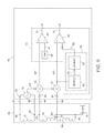
- FIG. 1 illustrates one example of an embodiment of a portion of a rotational system 10 that includes a proximity sensor system 12 and movable object.
- the movable object may be a wheel 11 that has protrusions.
- the protrusions may be teeth such as teeth of a gear that may be used to drive rotation of wheel 11 .
- a top view 13 also illustrates proximity sensor system 12 and wheel 11 along with teeth 14 and 15 .
- sensor system 12 includes sensor elements and a sensor circuit that can be used to determine if wheel 11 is moving and the direction of the movement.
- FIG. 2 schematically illustrates an example of an embodiment of a portion of sensing system 120 that may be an embodiment of a portion of system 12 of FIG. 1 .
- An embodiment of system 120 includes a sensor circuit 127 and sensor elements 121 .
- An embodiment of sensor circuit 127 may include a first receiver circuit 133 that is configured to receive a first signal 134 that is representative of a first variable mutual inductance of a sensor 123 and form a first detection signal 135 that is representative of the first variable mutual inductance.
- signal 134 may be a differential a.c. signal received form sensor 123 and signal 135 may be a differential a.c. signal that swings around a common mode voltage.
- the common mode voltage may be ground or some other voltage value.
- signal 135 may be a rectified d.c. signal that is referenced to a common voltage such as for example a ground reference.
- An embodiment may include that the first variable mutual inductance varies in response to a position of a target object.
- the target object may be a metal object.
- the target object may be a ferromagnetic material or alternately may be a conductive material.
- circuit 127 may also include a recognition circuit 143 that is configured to assert a movement detected signal 144 responsively to a first value of first detection signal 135 .
- circuit 143 may form signal 144 to have an asserted value in response to the value of signal 135 being greater than a first threshold signal.
- circuit 127 may include a signal generator circuit 129 that is configured to generate an excitation signal 130 .
- Circuit 127 may be configured to apply excitation signal 130 to an excitation element 122 .
- the first variable mutual inductance may be formed between excitation element 122 and a first receiver sensor 123 that is configured to form signal 134 .
- An embodiment of circuit 127 may also include a second receiver circuit 138 configured to receive a second signal 139 that is representative of a second variable mutual inductance and form a second detection signal 140 that is representative of the second variable mutual inductance.
- signal 139 may be a differential a.c. signal received from sensor 124 that swings around a common mode voltage and signal 140 may be a differential a.c.
- the common mode voltage may be ground or some other voltage value.
- signal 135 may be a rectified d.c. signal that is referenced to a common voltage such as for example a ground reference.
- the second variable mutual inductance varies in response to the position of the target object.
- the second variable mutual inductance may be formed between excitation element 122 and a second receiver sensor 124 that is configured to form signal 139 .
- receiver sensors 123 and 124 may form signals that may be referenced to a common signal or sensor reference signal received from a sensor reference circuit or sensor reference or SRef 127 .
- circuit 143 may also be configured to assert a movement direction signal 145 responsively to a first value of second detection signal 140 .
- FIG. 3 graphically illustrates some examples of embodiments of a portion of a combination of sensor elements that may be an example of alternate embodiments for sensor elements 121 of FIG. 2 .
- FIG. 3 illustrates a plan view of one possible geometric shape that may be used to form an embodiment of an excitation element 16 , an example of a possible geometric shape that may be used to form an embodiment of a first receiver sensor 18 , and an example of a possible geometric shape that may be used to form an embodiment of a second receiver sensor 30 .
- Element 16 and sensors 18 and 30 may be alternate embodiments of respective element 122 and sensors 123 and 124 of FIG. 2 .
- Element 16 and sensor 18 are configured to be positioned adjacent each other and to form a mutual magnetic coupling or mutual inductance between element 16 and sensor 18 .
- Sensor 30 is configured to have a mutual magnetic coupling or mutual inductance to element 16 that is different from the coupling between element 16 and sensor 18 .
- the shapes of element 16 and sensors 18 and 30 are chosen such that the mutual inductance between element 16 and sensor 18 and the mutual inductance between element 16 and sensor varies as the target object in placed in different positions relative to sensors 18 and 30 .
- the relative positions of element 16 and sensors 18 and 30 is also chosen so that the mutual inductance varies responsively to positions of the target object.
- element 16 is formed in a geometric shape of substantially a circle.
- Element 16 has a periphery 17 that has the geometric shape.
- the geometric shape of element 16 also has an area.
- element 16 may be formed from a conductor such as a wire or as a conductive trace on a PC board.
- the conductor may be formed into a loop that has the geometric shape and that may be used as an inductor. Two opposite ends of the conductor form connection terminals 28 and 29 that can be used to form an electrical connection to element 16 .
- Receiver sensor 18 is formed to have more loops that element 16 .
- Receiver sensor 18 is also formed to have a periphery 20 that has a geometric shape.
- periphery 20 of sensor 18 has substantially the same shape as the periphery of element 16 .
- the geometric shape of sensor 18 may have substantially the same area as element 16 .
- sensor 18 is formed to have more loops than element 16 .
- sensor 18 has two loops. In an embodiment, the two loops may be positioned adjacent each other. An embodiment may include that the two loops are positioned laterally adjacent to each other and in the same plane.
- a first loop 22 may extend from a connection terminal 26 around a left portion of periphery 20 to substantially a mid-point of periphery and then extends toward terminal 26 until reaching a cross-over portion 23 of the first loop 22 .
- the mid-point of periphery 20 may be substantially laterally across from terminal 26 .
- An embodiment may include that loop 22 has an area that is substantially one-half of the area of sensor 18 .
- a second loop 21 may extend from a connection terminal 25 away from portion 23 and around a right portion of periphery 20 to substantially a mid-point of periphery 20 and then extend to cross-over portion 23 .
- An embodiment may include that loop 21 has an area that is substantially one-half of the area of sensor 18 .
- Cross-over portion 23 forms an electrical and physical connection between loops 21 and 22 .
- An embodiment may include that loops 21 and 22 each have a shape of substantially a mushroom cap with the two mushroom caps positioned in a back-to-back configuration.
- sensor 18 may have a geometric shape that is a twisted and rotated image of element 16 .
- sensor 18 can be envisioned by twisting element 16 about an axis 97 (illustrated in a general manner by a dashed line) and pushing periphery 20 into the desired geometric shape.
- An embodiment may include forming sensor 18 in a shape such that when placed adjacent to but not electrically shorted to element 16 , a mutual inductance formed between element 16 and sensor 18 is a null value. In one embodiment the mutual inductance may be substantially zero. Those skilled in the art will appreciate that because of manufacturing tolerances and other variations, the null value may not be identically zero buy may be near zero, or alternately substantially zero.
- An embodiment may include forming 22 as conductor loop wound in a first direction, such as for example a counter-clockwise direction, and forming loop 21 as a conductor loop wound in a second direction, such as for example a clockwise direction.
- the mutual inductance between element 16 and sensor 18 may be substantially a null mutual inductance in response to no target object near to sensor 18 or near to any of loops 21 - 22 . In one embodiment, the mutual inductance may be substantially zero.
- the signal applied to element 16 forms a magnetic field. Because of the symmetrical shape of loops 21 and 22 , loop 22 may be considered as a loop that forms a signal of a first polarity and loop 21 may be considered as a loop that forms a signal of a second and substantially opposite polarity. This can also be regarded as substantially symmetry of the loops.
- any signals induced into loops 21 and 22 will form substantially equal signals of opposite polarity in loops 21 and 22 . These opposite signals will cancel out and the signal between terminals and 26 will substantially zero.
- the magnetic field from element 16 forms a current in the target object which then forms a magnetic field from the target object.
- the mutual inductance between element 16 and loop 22 may be increased and the signal between terminals 25 and 26 will responsively increase.
- the mutual inductance may be a maximum value if the target object is placed solely under the center of loop 22 . In an embodiment, the maximum value has a magnitude that is greater than the null value.
- the signal between terminals 25 - 26 may also have a maximum amplitude. If the target object is positioned substantially under the center of sensor 18 the mutual inductance may be substantially the null value or alternately substantially zero. The signal between terminals 25 and 26 may also have a substantially zero amplitude. If the target object is positioned under loop 21 , the magnitude of the mutual inductance may have a minimum value. Thus, the amplitude may be greater than the null value but the polarity may be reversed with respect to the polarity of the maximum value. Consequently, the polarity of the signal between terminals 25 and 26 may be reversed. For example, the direction of a current or a voltage formed between terminals 25 and 26 may be reversed.
- the signal between terminals 25 and 26 is an a.c. signal that may be referenced to any value of reference signal.
- the signal may be referenced to ground or to a negative supply voltage or a positive supply voltage.
- the minimum value may have an amplitude or magnitude similar to the amplitude of the maximum mutual inductance but the polarity may be reversed with respect to the polarity of the maximum value.
- An embodiment may include that the mutual inductance may have a positive value as the maximum value, a non-positive value (relative to the positive value) as the minimum value, and the null value may be some threshold value that is between the maximum and minimum values.
- the signal between terminals 25 and 26 may have a maximum value, a minimum value, and a null value that is a threshold value that is between the maximum and minimum values of the signal.
- noise signals induced into sensor 18 will be cancelled within sensor 18 . Because of the symmetry of loops 21 and 22 , the noise signals will form substantially equal signals of opposite polarity in loops 21 and 22 . These opposite signals will cancel out and the signal between terminals 25 and 26 will be substantially devoid of the noise signals.
- the noise signal may be from a cellular telephone or signals produced during the operation of an automobile engine, or other source.
- Receiver sensor 30 may be formed from a conductor that is also formed into a plurality of loops.
- sensor 30 may also have two loops.
- Sensor 30 is also formed to have a periphery 42 that has a geometric shape.
- periphery 42 of sensor 30 has substantially the same geometric shape as element 16 .
- the portions of the conductor that are included in each loop may be electrically connected together by cross-over portions of the conductor.
- An embodiment may include that the two loops may be positioned laterally adjacent to each other.
- a first loop 37 may have a shape of substantially a mushroom cap attached to one-half of a rectangle. Loop 37 may have other shapes in other embodiments.
- a first portion 38 of loop 37 may extend from a connection terminal 41 around a left portion of periphery 42 to a first point along periphery 42 and then extend inward toward a first cross-over portion 33 of first loop 37 to a second portion 39 of loop 37 .
- the first point along the periphery may be approximately one-fourth of the distance around periphery 42 .
- An embodiment may include that loop 37 has an area of approximately one-half the area of sensor 30 .
- a second loop 34 of sensor 30 may also have a shape of substantially a mushroom cap attached to a second half of the rectangle. Loop 34 may have other shapes in other embodiments.
- a first portion 36 of loop 34 may extend from a connection terminal 40 outward away from cross-over portion 33 toward periphery 42 , around one-fourth of periphery 42 and then extend inward away from periphery 42 to a cross-over portion 31 of loop 34 .
- This first portion 36 may form a shape of one-half of a rectangle.
- a second portion 35 of loop 34 may have the substantially mushroom cap shape and may extend from cross-over portion 31 outward at an angle toward periphery 42 , around approximately one-fourth of periphery 42 and then inward to a third cross-over portion 32 to connect to loop 37 .
- a midpoint of portion 35 of loop 34 may be directly opposite a midpoint of portion 38 of loop 37 such that a line through the two midpoints would bisect the center of sensor 30 .
- An embodiment may include that loop 34 has an area of approximately one-half the area of sensor 30 .
- loops 34 and 37 may have substantial the same planar area. However, in some embodiments, the area of portions 35 and 38 may be different from the area of portions 36 and 39 .
- Cross-over portion 32 forms a connection between loops 34 and 37 .
- Cross-over portions 31 and 33 form connections between respective portions 35 and 36 and portions 38 and 39 of respective loops 34 and 37 .
- An embodiment may include forming portions 36 and 38 as conductor loop portions wound in a first direction, such as for example a counter-clockwise direction, and forming portions 35 and 39 as conductor loop portions wound in a second direction, such as for example a clockwise direction.
- An embodiment may include forming loops 34 and 37 to each have clockwise and counter-clockwise portions that substantially cancel out the mutual inductance from the opposite direction portion of each loop.
- sensor 30 may have a geometric shape that is a multiple twisted and rotated image of element 16 .
- sensor 30 can be envisioned by twisting a top portion of element 16 about an axis 95 (illustrated in a general manner by a dashed line) and then twisting a bottom portion of element 16 about an axis 96 (illustrated in a general manner by a dashed line), and then pushing periphery 42 into the desired geometric shape.
- An embodiment may include forming sensor 30 in a geometric shape such that when placed adjacent to but not electrically shorted to element 16 , a mutual inductance formed between element 16 and sensor 20 is a minimum value. In one embodiment the mutual inductance may be substantially zero.
- the mutual inductance between element 16 and sensor 30 may be substantially a null mutual inductance in response to no target object near to sensor 30 or any of loops 34 - 36 . In one embodiment, the mutual inductance may be substantially zero.
- Sensor 30 is also formed to have symmetry of the loops. Portions 35 and 38 may be considered as loop portions that form signal of a first polarity and portions 36 and 39 may be considered as a loop portions that form a signal of a second and substantially opposite polarity. Thus each of loops 34 and 37 have symmetrical loops or loop portions.
- the mutual inductance may be a maximum value if the target object is placed solely under the center of portion 38 . Also, if the target object is positioned substantially under the center of portion 35 , the mutual inductance is also increased in respect to the null mutual inductance value. If the target object is placed substantially under the center of portions 36 and 39 , the mutual inductance may be decreased in respect to the null value. In an embodiment, the mutual inductance may be minimum if the target object is placed substantially under the center of portions 36 and 39 . As will be seen further hereinafter, the minimum value has a large absolute value but a polarity that is opposite to the maximum value. For example, the polarity may be negative in respect to the null value.
- noise signals induced into sensor 30 will be substantially cancelled within sensor 30 .
- the noise signals will form a substantially equal signal of opposite polarity in the loop portions. These opposite signals will cancel out and the signal between terminals 40 and 41 will substantially devoid of the noise signals.
- FIG. 4 graphically illustrates a portion of an example of an embodiment of some configurations of sensor elements 121 of FIG. 1 .
- element 16 and sensors 18 and 30 may be formed in an overlying configuration relative to each other.
- Sensor 30 may be positioned to be facing the target object, illustrated as the example of wheel 11 ( FIG. 1 ).
- Sensor 18 may be positioned overlying sensor 30 .
- Element 16 may be positioned overlying sensor 18 .
- the combination of element 16 and sensors 18 and 30 may be positioned such that the movement of teeth 14 - 15 is in a direction that traverses laterally across substantially the center of loops 22 and 21 , and substantially across substantially the center of loops 34 and 37 .
- the target object may traverse under loops 22 and 21 and loops 34 and 37 in the direction of an arrow 44 .
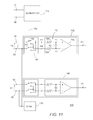
- FIG. 5 schematically illustrates an example of an embodiment of a portion of a sensor circuit 45 that may be an alternate embodiment of circuit 127 that was explained the description of FIG. 2 .
- Circuit 45 includes a signal generator 52 that is configured to form an excitation signal 53 .
- Generator 52 may be an alternate embodiment of generator 129 that was explained in the description of FIG. 2 .
- circuit 45 is configured to operate with sensor elements 75 that are similar to sensor elements 121 that were explained in the description of FIG. 2 .
- Sensor elements 75 may include a sensor reference circuit of sensor reference or SRef 76 that is similar to and that operates similarly to Sref 127 ( FIG. 2 ).
- circuit may include terminals 47 and 48 that are configured for connecting to respective terminals 28 and 29 of element 16 .
- a terminal 49 of circuit 45 may be configured for receiving a signal from terminal 25 of sensor 18 and a terminal 50 of circuit 45 may be configured for receiving a signal from terminal 41 of sensor 30 .
- Terminals 26 and of respective sensors 18 and 30 may be connected to a common reference voltage such as a ground reference or other common reference used for operating circuit 45 .
- terminals 26 and 40 may be connected to other elements of circuit 45 .
- circuit 45 may receive the differential a.c. signals from terminals 25 and 26 of sensor 18 and from terminals 40 and 41 of sensor 30 and process the differential signals instead of referencing the signals from sensors 18 and 30 to a ground reference.
- Circuit 45 also includes a recognition circuit 72 that is an alternate embodiment of circuit 143 that was described in the description of FIG. 2 and operates similarly to circuit 143 .
- a demodulator circuit or demodulator 55 and a demodulator circuit or demodulator 57 of circuit 45 are alternate embodiments of respective circuits 133 and 138 that were explained in the description of FIG. 2 and operate similarly to circuits 133 and 138 .
- circuit 72 may include a comparator 60 and a comparator 62 .
- a reference signal generator or reference or ref 58 may be utilized to form a reference signal 59 for comparator 60 .
- circuit 72 may include a reference circuit 68 that is configured to form a reference signal 65 for comparator 62 .
- reference circuit 68 may be an adaptable reference circuit 68 that is configured to form an adaptable reference signal 65 for comparator 62 .
- An embodiment of the operation of circuit 45 may include that generator 52 is configured to couple excitation signal 53 to excitation element 16 .
- signal 53 may be an a.c. signal.
- the frequency of the a.c. signal is greater than a frequency at which a target object moves under sensors 18 and/or 30 .
- the frequency of the a.c. signal may be between approximately one and approximately ten megahertz (1-10 MHz).
- demodulator 55 is configured to receive excitation signal 53 and to receive a receiver signal 46 from sensor 18 .
- Demodulator 55 is configured to demodulate signal 46 and form a detection signal D 1 that is representative of the mutual inductance of sensor 18 .
- this mutual inductance may be the mutual inductance between sensor 18 and element 16 .
- demodulator 57 may be configured to receive signal 53 and to receive a receiver signal 51 from sensor 30 .
- Demodulator 57 may be configured to demodulate signal 51 and form a detection signal D 2 that is representative of the mutual inductance of sensor 30 .
- this mutual inductance may be the mutual inductance between sensor 30 and element 16 .
- demodulators 55 and 57 may be formed to demodulate the respective received signals 46 and 51 from respective sensors 18 and 30 , and to form a.c. signals that swing around a common reference signal.
- signals D 1 and D 2 are a.c.
- demodulators 55 and 57 may receive differential signals from respective sensors 18 and 30 and form signals D 1 and D 2 as a.c. signals that have peak and valley values around a common mode voltage.
- the common mode voltage may be ground or may be signal 59 or may be some other voltage value.
- An embodiment of demodulators 55 and 57 may include forming the demodulators to demodulate the respective received signals 46 and 51 from respective sensors 18 and 30 , and to optionally rectify the demodulated signals to form a slowly varying signal that is representative of the mutual inductance of respective sensors 18 and 30 .
- the value of the signal may vary as the target object moves.
- demodulators 55 and 57 may form the signal as a varying d.c. signal that is representative of the mutual inductance of respective sensors 18 and 30 .
- FIG. 6 is a graph having plots that illustrate some of the signals formed by circuit 45 .
- the abscissa indicates increasing time and the ordinate indicates the amplitude and polarity of the corresponding signals.
- a plot 80 illustrates an example embodiment of the mutual inductance of sensor 18 and a plot 81 illustrates an example embodiment of the mutual inductance of sensor 30 .
- a plot 82 illustrates an example embodiment of detection signal D 1 and a plot 83 illustrates an example embodiment of detection signal D 2 .
- the embodiment of signal D 1 illustrated in FIG. 6 is formed to be an a.c. signal that has peak and valley values that are referenced to and that are respectively greater than and less than the value of reference signal 59 .
- FIGS. 3-6 is formed to be an a.c. signal that has peak and valley values that are referenced to and that are respectively greater than and less than the value of reference signal 65 .
- a plot 86 illustrates signal 61 and a plot 87 illustrates signal 63 . This description has references to FIGS. 3-6 .
- the target object is a toothed wheel similar to wheel 11 that is illustrated in FIG. 1 and that circuit 45 and elements 75 are configured to detect movement of wheel 11 . Also, assume that a width (W) of each tooth of wheel 11 ( FIG. 1 ) is less than a diameter 27 ( FIG. 3 ) of element 16 and sensors 18 and 30 .
- the mutual inductance of sensor 18 is substantially a null value as illustrated by plot 80 at t 0 .
- the null value may be near a zero mutual inductance value and in an embodiment the null value may be substantially zero.
- the null value may be a value that is substantially an average value of the mutual inductance.
- signal D 1 also has a null value as illustrated by plot 82 at t 0 .
- signal D 1 correspondingly may have a value that is substantially signal 59 . Consequently, signal D 1 is no greater than reference signal 59 which causes the output of comparator 60 to be negated as illustrated by plot 86 .
- the exact value of signal D 1 which causes the negating or asserting of signal 61 is determined by the value of signal 59 .
- signal 59 may have a value that is between the anticipated peak and valley values of signal D 1 . For example, signal 59 may be a percentage of the difference between the peak and minimum or valley value of signal D 1 .
- the value of signal 59 may be near a midpoint of the power supply used for operating comparator 60 .
- the value of signal 59 may be a ground value for the case of differential signals D 1 and D 2 that may swing above and below ground, or may be other values in other embodiments.
- the mutual inductance of sensor 30 is a maximum value as illustrated by plot 81 at t 0 . Consequently, signal D 2 also has a maximum value as illustrated by plot 83 at t 0 . Since signal D 2 is greater than reference signal 65 , direction signal 63 is asserted.
- the mutual inductance may be a maximum or peak value.
- the center of the tooth is also moving from the center of portion 38 toward portions 36 and 39 of sensor 30 which continues decreasing the value of the mutual inductance as illustrated by plot 81 between t 0 and t 1 .
- signal D 2 also decreases in value as illustrated by plot 83 .
- comparator 62 may negate signal 63 .
- the tooth moves from under the center of loop 22 of sensor 18 to under the actual center of sensor 18 , also the tooth also moves from portion 38 of sensor 30 to under the center of portions 36 and 39 .
- Positioning the tooth under the center of sensor 18 forms a null mutual inductance as illustrated by plot 80 at t 2 .
- the null value may be near to a zero value of mutual inductance or in some embodiments may be approximately a zero mutual inductance.
- the value of signal D 1 also has a value that is near to the common mode value of signal D 1 , such as for example near to the value of signal 59 , as illustrated by plot 82 at t 2 .
- the value of D 1 may be substantially zero.
- signal 61 is negated.
- the tooth having a position under portions 36 and 39 of sensor 30 forms a minimum mutual inductance for sensor 30 as illustrated by plot 81 at t 2 . Consequently, the value of signal D 2 decreases as illustrated by plot 83 at t 2 .
- Circuit 72 maintains signal 63 negated since the value of signal D 2 is less than signal 65 .
- the tooth moving from under portions 36 and 39 of sensor 30 to under portion 35 increases the mutual inductance of sensor 30 from the minimum mutual inductance toward a null mutual inductance as illustrated by plot 81 from t 2 to t 3 .
- Signal D 2 responsively increases from a minimum value or valley value at t 2 to a value at t 3 that is near to signal 65 as illustrated by plot 83 .
- signal D 2 may have a substantially zero value at t 3 .
- Signal 63 may remain negated as signal D 2 increases and may be asserted in response to D 2 having a value no less than signal 65 as illustrated by plot 87 between t 2 and t 3
- the wheel continues to rotate and the tooth moves from the center of loop 21 of sensor 18 toward the periphery of sensor 18 and to outside the periphery near time t 4 .
- the mutual inductance of sensor 18 increases from the minimum toward a null value as illustrated by plot 80 between t 3 and t 4 , and becomes substantially a null value when no tooth is under sensor 18 as illustrated at t 4 .
- the mutual inductance becomes substantially zero.
- Detection signal D 1 increases toward the value of signal 59 and becomes no less than signal 59 which results in asserting signal 61 near or just after time t 4 .
- reference circuit 68 may be an adaptable reference circuit 68 that forms an adaptable value for reference signal 65 .
- the peak excursions of the mutual inductance of sensor 30 may not be equal and the resulting maximum and minimum values of signal 51 may not all be equal in magnitude.
- Adaptable reference circuit 68 is configured to form adaptable reference signal 65 to have a value that is somewhere between the maximum and minimum values of signal D 2 .
- circuit 68 may form signal 65 to have a value that is a percentage of the maximum peak values of signal D 2 .
- An embodiment may include that signal 65 is formed to have a value that is an average value of signal D 2 .
- Circuit 68 may include a detect circuit 69 and an adjust circuit 64 .
- Detect circuit 69 may be configured to sample signal D 2 and form an average of the peak values of signal D 2 .
- detect circuit 69 may be a sample-and-hold circuit that samples the peak values of signal D 2 and forms an average value of the peak values.
- circuit 69 may be other circuits that can form an average of signal D 2 , such as for example an analog-to-digital converter and digital logic or optionally a digital memory circuit.
- Adjust circuit 64 may be configured to adjust the averaged peak values by some percent to form signal 65 . An embodiment may include that the percentage is approximately one-half but may be other values in other embodiments.
- FIG. 7 is a graph that illustrates an example embodiment of variations of signal 65 .
- a plot 88 illustrates the mutual inductance of sensor 30 and variations that may occur in the mutual inductance.
- a plot 89 illustrates variations in the maximum value of the mutual inductance and a plot 90 illustrates variations in the minimum value of the mutual inductance.
- the non-symmetrical shape of the mutual inductance of sensor 30 will also be translated to unequal peak values of signal D 2 .
- a plot 84 illustrates one example of changes to the value of signal 65 in response to the variations of the mutual inductance of sensor 30 , or alternately to the variations in the maximum and minimum values of signal D 2 .
- circuit 64 is configured to decrease the value of signal 65 in response to a decrease in signal D 2 and to increase signal 65 in response to an increase in the value of signal D 2 .
- circuit 45 receiving differential signals from sensors 18 and 30 and for signals D 1 and D 2 having differential values around a common mode voltage.
- comparator 60 Each time a crossing of the common mode voltage, such as substantially a zero crossing for example, is detected by comparator 60 , comparator 62 determines the polarity of the signal from sensor 30 . This polarity can be used to show the direction of the tooth wheel rotation.
- a plot 77 illustrates the mutual inductance of sensor for another example embodiment. Assume that wheel 11 is rotating and that at a point 78 , wheel 11 begins to rotate in an opposite direction. The change in direction causes a change in the mutual inductance sensed by sensor 30 , and a corresponding change in the peak value of signal D 2 . The change in the peak value of D 2 also causes a change in the value of signal 65 . Since the peak value of signal D 2 has decreased, the value of reference signal 65 is also decreased. The decrease in signal 65 may be used to indicate that the direction of wheel 11 has changed.
- FIG. 8 illustrates portions of other example embodiments of sensor 30 .
- the teeth width and gap width may be positioned differently, thus, the mutual inductance between element 16 and sensor 30 may not be null when the tooth edge is in the middle of sensor 30 , but the position that provides the null value may be shifted to the left or to the right.
- the substantial minimum mutual inductance may occur for the tooth edge shifted to the right or to the left of sensor 30 .
- the layout of sensor can be modified.
- portions 36 and 39 can be made narrower while portion 35 and/or portion 38 can be larger or vice versa as illustrated by alternated embodiments 30 A- 30 C of sensor 30 .
- Portions 36 and 39 may be such that the mutual inductance stays substantially minimized or substantially null without metal in proximity.
- sensors 18 and 30 may be formed by printing conductive traces on a PC board.
- one of sensors 18 or 30 may be formed by printing traces in first direction, such as for example a clockwise direction, on the PC board.
- the other one of sensors 18 or 30 may be printed in the opposite direction, such as for example a counter-clockwise direction, on an overlying or underlying layer of the PC board.
- the two sensors may then be overlaid and appropriately connected to terminals, etc.
- FIG. 9 illustrates an exploded view of an example of an embodiment of a printed circuit (PC) board 99 on which element 16 and sensors 18 and 30 may be formed.
- Element 16 and sensors 18 and 30 may be formed in various geometric shapes and relative positions in addition to those illustrated in FIG. 3 and FIG. 4 .
- board 99 may be formed as a multilayer PC board that includes a main substrate 100 on which sensor may be formed such as for example as a conductive trace formed on substrate 100 .
- An insulating layer 102 may be formed overlying sensor 30 .
- layer 102 may be an epoxy resin that is formed on board 100 and covering sensor 30 .
- sensor 18 may be formed within and in the same plane with element 16 .
- Element 16 and sensor 18 also may be formed as conductor traces on layer 102 .
- Element 16 and sensors 18 and 30 may have other geometric shapes.
- the geometric shape may be a square or a rectangle or an ellipse or other shape other than the circular shape described hereinbefore.
- FIG. 10 illustrates an enlarged plan view of a portion of an embodiment of a semiconductor device or integrated circuit 110 that is formed on a semiconductor die 111 .
- Circuit 120 and/or circuit 45 is formed on die 111 .
- Die 111 may also include other circuits that are not shown in FIG. 9 for simplicity of the drawing.
- Circuit 45 and device or integrated circuit 110 are formed on die 111 by semiconductor manufacturing techniques that are well known to those skilled in the art.
- sensor element 75 and/or 122 or portions thereof may be formed on die 111 as illustrated by dashed lines.
- the target is illustrated and explained as a curved or circular wheel 11
- the target may be a linear object that has protrusions that are similar to teeth 14 and 15 .
- FIG. 11 schematically illustrates an example of an embodiment of a portion of a circuit 150 that may be an alternate embodiment of portions of circuit 45 that was explained in the description of FIG. 5 .
- Circuit 150 includes a signal generator or generator 175 that is an alternate embodiment of signal generator 52 .
- Generator 175 is configured to form an excitation signal 176 that is an alternate embodiment of signal 53 ( FIG. 5 ).
- the frequency of signal 176 is much greater than the frequency variation of the mutual inductance of sensor 18 .
- Circuit 150 also includes a demodulator circuit 152 that may be an alternate embodiment of demodulator 55 that was explained in the description of FIG. 5 and a demodulator circuit 168 that may be an alternate embodiment of demodulator 57 that was explained in the description of FIG. 5 .
- Circuit 150 may also include a sensor reference circuit or SRef 170 that is an alternate embodiment of SRef 76 ( FIG. 5 ).
- Demodulator 152 includes a low pass filer 172 , an amplifier 162 , and a switch circuit or switch 154 .
- SRef 170 forms a reference signal having a value that is between the value of the voltages supplied to operate amplifier 162 . For example, if amplifier 162 operates between five volts (5 V) and ground, SRef 170 may form a signal of approximately two and one-half volts (21 ⁇ 2 V). If amplifier 162 operates between a positive supply and a negative supply, SRef 170 may set supply a signal that is substantially ground or alternately a signal that is halfway in between the positive and negative supplies. Consequently, the value of signals 46 and 51 received from respective sensors 18 and 30 are reference to the value of the signal from SRef 170 .
- Switch 154 is configured to receive signal 176 and signal 46 from sensor 18 and couple the signals to amplifier 162 through low pass filter 172 .
- filter 172 may include a capacitor 164 and resistors 159 and 160 .
- sensor 18 generates signal 46 between terminals 49 and 26 such that terminal 49 is more positive than terminal 26 (as illustrated by a solid arrow).
- signal 176 control switches 156 and 157 to couple the more positive terminal of sensor 18 , such as for example terminal 49 , to the positive input of amplifier 162 and to couple the less negative terminal of sensor 18 , such as for example terminal 26 , to the inverting input of amplifier 172 .
- sensor 18 During the negated portion of signal 176 , sensor 18 generates signal 46 such that terminal 26 is more positive than terminal 49 (as illustrated by a dashed arrow). Also during the negated portion of signal 176 , signal 176 controls switches 156 and 157 to couple the more positive terminal of sensor 18 , such as for example terminal 26 , to the positive input of amplifier 162 and to couple the less positive terminal to the inverting input of amplifier 162 . Thus, amplifier 162 forms an output signal that is representative of the mutual inductance between sensor 18 and element 16 .
- the low pass filter may be formed by other means including using a digital signal processor (DSP) to implement the low pass filter. Additionally, the DSP may also be used for amplifier 162 and switch 154 .
- DSP digital signal processor
- Demodulator 168 is formed substantially similar to and operates substantially similar to demodulator 152 except that demodulator 168 is configured to receive the signals from sensor 30 instead of sensor 18 .
- the sensors may include that a common coil may be formed, such as by example as forming traces on a PCB.
- Another coil such as for example the coil of sensor 18 , may be formed to include of two loops.
- the first one, marked 22 may be counter-clock wise while the second one, marked 21 , may be clock wise or vice versa.
- the variation of the mutual inductance between the common coil and the center coil can be used to detect the middle of the tooth or the middle of the gap between two teeth.
- Another coil such as for example a coil of sensor 30 , may include three loops.
- a first and last loop, marked 36 may be counter-clock wise while the second one, marked 34 , may be clock wise or vice versa.
- a variation of the mutual inductance between the first coil and the second coil can be used to detect the edge of the teeth.
- One or more of the 3 coils can be made of multiple turns or loops to increase the sensitivity of the sensor.
- the position of the first and second coil may be different relative to a common coil.
- the first and second coils may be on the opposite side of the common coil.
- An embodiment may include that one of the coils, for example the second coil, includes a plurality of loops including a first loop and a second loop, the first loop may be formed as a conductor having a first end and a second end, the second loop may be formed as a conductor having a third end and a fourth end wherein the second end is coupled to the fourth end; the first loop having a first portion formed in a shape of a substantially half rectangle and a second portion formed in a shape of substantially a mushroom cap; and the second loop having a first portion formed in a shape of a substantially half rectangle and a second portion formed in a shape of substantially a mushroom cap wherein the first portion of the first loop and the first portion of the second loop are positioned to form a shape that is substantially a rectangle having two long sides and two short sides with an opening in the two long sides.
- the first conductor may be formed so that another portion of the conductor that is between the first portion and the second portion, is routed to run through the opening in one side of the rectangle.
- the second conductor could be similarly formed to route through the opening in an opposite side of the rectangle side.
- the common coil may be two mutual inductances between the common coil and the other two coils. Without any metal, such as the metal of a rotational element, in proximity to the coils the mutual inductances are null.
- the simple coil symmetry may assist in forming a null mutual inductance with the first coil.
- the relative loop sizes can be adjusted to assist in forming the null mutual inductance.
- the mutual inductance can be substantially maximum when a tooth aligns with the loop 22 and it may be substantially a minimum when the tooth aligns with the loop 21 .
- the center of the tooth aligns with the middle of the coil the mutual inductance is minimized and may be substantially null because of the coil and tooth symmetry.
- the mutual inductance may be substantially a maximum when teeth overlap with the first and last loops while the gap is aligned with the portions 36 and 39 .
- the mutual inductance may be substantially a minimum with the tooth in or near the middle. When the edge of the tooth substantially aligns with the middle of the coil the mutual inductance is substantially minimized or a substantial null because of symmetry.
- voltages will develop across the first and second coils in response to the position of the tooth (or teeth).
- These alternating voltages may be demodulated, such as for example by means of synchronous rectification with the oscillator.
- the demodulated (or in some embodiments rectified) signals can then be connected to comparators inputs ‘+’.
- the comparators inputs ‘ ⁇ ’ may be referenced to the common reference, such as for example to ground reference, if the zeroing of the mutual inductance has been realized. If it's not possible or there is a slow varying signal superposed (for example due to the eccentricity of the tooth wheel) an adaptive threshold may be implemented.
- the substantial maximum and the substantial minimum values of the signals can be measured and stored in a peak & valley block.
- the peak & valley block can be an analog sample and hold or an ADC and digital memory. Based on these two values, for example the peak and valley values) a threshold may be calculated (for example average of peak and valley).
- the second comparator determines the polarity of the center coil signal. This polarity can be used to show the direction of the tooth wheel rotation.
- the edge and center coils connections to the sensor interface circuit can be swapped.
- the symmetry of the first and second sensors along with the excitation element can improve the sensitivity of the sensor elements in respect to prior elements.
- the improved sensitivity can facilitate placing the sensor elements further away from the target object than prior elements.
- the improved sensitivity may also reduce the power dissipation over that of prior elements.
- a position and rotational direction sensor may comprise:
- first coil configured for positioning a first distance from a rotational element; a second coil configured for positioning a second distance from the rotational element; a third coil configured for positioning a third distance from the rotational element wherein the second distance is greater than the first distance and the third distance is greater than the second distance; one of the first or third coils including a plurality of loops including a first loop and a second loop, the first loop formed as a conductor having a first end and a second end, the second loop formed as a conductor having a third end and a fourth end wherein the second end is coupled to the fourth end; the first loop having a first portion formed in a shape of a substantially half rectangle and a second portion formed in a shape of substantially a mushroom cap; and the second loop having a first portion formed in a shape of a substantially half rectangle and a second portion formed in a shape of substantially a mushroom cap wherein the first portion of the first loop and the first portion of the second loop are positioned to form a shape that is substantially a rectangle having
- the position and rotational direction sensor may include that the second coil is formed from a conductor having two portions where a first portion forms a shape of substantially a mushroom cap and the second portion also forms a mushroom cap shape with a base portion of both of the mushroom shapes facing substantially together.
- Another embodiment may include that the first coil may have at least three loops.
- the first coil may be a common coil.
- Another embodiment may include that a width of the first loop of the plurality of loops is greater than the second loop of the plurality of loops.
- an embodiment of a device for detecting rotation of an object may comprise:
- a semiconductor device having a sensor circuit, such as for example circuit 45 , that includes a signal generator, such as for example generator 52 , configured to generate an excitation signal, such as for example signal 53 ;
- a first terminal, such as for example terminal 47 , of the sensor circuit configured to couple the excitation signal to an excitation element, such as for example element 16 ;
- a first demodulator such as for example demodulator 55 of the sensor circuit configured to receive the excitation signal and to receive a first receiver signal, such as for example at signal 46 , from a first receiver sensor, such as for example sensor 18 , wherein the first receiver signal is representative of a first mutual inductance that is formed between the excitation element and the first receiver sensor, the first demodulator configured to form a first detection signal, such as for example signal D 1 , that is representative of the first mutual inductance;
- a second demodulator such as for example demodulator 57 of the sensor circuit configured to receive the excitation signal and to receive a second receiver signal, such as for example signal 51 , from a second receiver sensor, such as for example sensor 30 , wherein the second receiver signal is representative of a second mutual inductance that is formed between the excitation element and the second receiver sensor, the second demodulator configured to form a second detection signal, such as for example signal D 2 , that is representative of the second mutual inductance;
- the sensor circuit configured to assert a rotation detected signal, such as for example signal 61 , responsively to a difference between the first detection signal and a first reference signal, such as for example signal 59 ;
- the sensor circuit configured to assert a rotation direction signal, such as for example signal 63 , responsively to a difference between the second detection signal and an adaptable reference signal, such as for example signal 65 .
- the device may include a first comparator, such as for example comparator 60 , configured to receive the first detection signal and the first reference signal and form the rotation detected signal on an output of the first comparator.
- a first comparator such as for example comparator 60
- Another embodiment may include a second comparator, such as for example comparator 62 , configured to receive the second detection signal and the adaptable reference signal and form the rotation direction signal on an output of the second comparator.
- a second comparator such as for example comparator 62
- An embodiment may include that the excitation element has a first geometric shape and the first receiver sensor has a second geometric shape that is substantially a twisted image of the first geometric shape.
- the second receiver sensor may have a third geometric shape that is substantially a twisted image of the second geometric shape.
- Another embodiment may include that the first demodulator may be configured to remove an a.c. component of the excitation signal from the first receiver signal.
- An embodiment may include that the signal generator may be configured to form an a.c. signal having a frequency that is greater than a first frequency at which the first mutual inductance varies and greater that a second frequency at which the second mutual inductance varies and wherein the a. c. component removed by the first demodulator corresponds the a. c. signal.
- the second demodulator may be configured to remove an a.c. component of the excitation signal from the second receiver signal.
- An embodiment may include that the adaptable reference circuit forms an average signal that is substantially an average value of the second detection signal and forms the adaptable reference signal substantially equal to the average signal.
- the sensor circuit such as for example circuit 45 , to receive a first receiver signal, such as for example signal 46 , from a first receiver sensor, such as for example sensor 18 , and form a first detection signal, such as for example signal D 1 , wherein the first detection signal has a magnitude that increases in response to a metal object moving from distal to the first receiver sensor to proximal to a first portion, such as for example loop 22 or 21 , of the first receiver sensor, wherein the magnitude of the first detection signal decreases in response to the metal object moving toward substantially a center, such as for example portion 23 , of the first receiver sensor;
- a rotation detection signal such as for example signal 61
- a first value such as for example the value of signal 59
- forming the sensor circuit to receive a second receiver signal, such as for example signal 51 , from a second receiver sensor, such as for example sensor 30 , and form a second detection signal, such as for example signal D 2 , wherein the second detection signal has a minimum value in response to the metal object in a position substantially centered to the second receiver sensor, and has a greater value in response to the metal object having a position distal from the center of the second receiver sensor; and
- a rotation direction signal such as for example signal 63
- a first value such as for example the value of signal 65
- An embodiment of the method may include configuring an adaptable reference circuit, such as for example circuit 68 , to form an adaptable reference signal, such as for example signal 65 , having a value that is a percentage of a difference between the greater value of the second detection signal and the minimum value of the second detection signal wherein the first value of the second detection signal is substantially equal to the value of the adaptable reference signal.
- Another embodiment may include configuring an adaptable reference circuit, such as for example circuit 68 , to form an adaptable reference signal, such as for example signal 65 , having a value that is an average of a maximum value and the minimum value of the second detection signal wherein the first value of the second detection signal is substantially equal to the value of the adaptable reference signal.
- an adaptable reference circuit such as for example circuit 68
- an adaptable reference signal such as for example signal 65
- the method may include configuring the sensor circuit to form the first detection signal to include a minimum value in response to the metal object in a position substantially centered to the first receiver sensor and in response to the metal object being distal to the first receiver sensor.
- Another embodiment may include configuring the sensor circuit to form the first detection signal to correspond to a mutual inductance formed between the first receiver sensor and an excitation element and to form the second detection signal to correspond to another mutual inductance formed between the second receiver sensor and the excitation element.
- a sensor circuit may comprise:
- a first receiver circuit configured to receive a first signal that is representative of a first mutual inductance and form a first detection signal that is representative of the first mutual inductance, wherein the first variable mutual inductance varies in response to a position of a metal object;
- a second receiver circuit configured to receive a second signal that is representative of a second mutual inductance and form a second detection signal that is representative of the second mutual inductance, wherein the second mutual inductance varies in response to the position of the metal object;
- a recognition circuit such as for example 72 , configured to assert a movement detected signal, such as for example 61 , responsively to a first value of the first detection signal, such as for example D 1 , configured to assert a movement direction signal, such as for example 63 , responsively to a first value of the second detection signal, such as for example D 2 .
- An embodiment may include that the first detection signal has a minimum value and a maximum value that are offset in phase with respect to a minimum value and a maximum value, respectively, of the second detection signal.
- Another embodiment may include that the first mutual inductance is formed between an excitation element having a first inductor including at least one inductor loop and a first receiver sensor having a second inductor including a second loop that has more than at least one inductor loop; and the second mutual inductance formed between the excitation element and a second receiver sensor having a third inductor including a third loop that has more than at least one inductor loop.
- the excitation element may be positioned adjacent to the first receiver sensor, and the first receiver sensor is positioned between the second receiver sensor and the excitation element.
- an excitation element configured to receive an a.c. signal from a sensor circuit and form a magnetic field
- a first receiver sensor such as for example sensor 18 , configured to have a first mutual inductance with the excitation element, the first receiver sensor including a first loop, such as for example loop 22 , that is wound in a first direction and having a second loop, such as for example loop 21 , that is wound in a second direction that is substantially opposite to the first direction such that the first mutual inductance is substantially null in an absence of the target object; and
- a second receiver sensor such as for example sensor 30 , configured to have a second mutual inductance with the excitation element
- the second receiver sensor including a third loop, such as for example loop 37 , having a first portion, such as for example portion 38 , that is wound in a third direction and a second portion, such as for example portion 39 , that is wound in a fourth direction that is substantially opposite to the third direction, and including a fourth loop, such as for example loop 34 , having a third portion, such as for example portion 36 , that is wound in substantially the third direction and a fourth portion, such as for example portion 35 , that is wound substantially in the fourth direction such that the second mutual inductance is substantially null in an absence of the target object.
- an excitation element configured to receive an a.c. signal from a sensor circuit and form a magnetic field
- a first receiver sensor such as for example sensor 18
- the first receiver sensor may be configured to have a first mutual inductance with the excitation element
- the first receiver sensor may include a first loop, such as for example loop 22 , that is wound in a first direction, such as for example counter clockwise, and having a second loop, such as for example loop 21 , that is wound in a second direction that is substantially opposite to the first direction such that the first mutual inductance is substantially null in the absence of the target object;
- a second receiver sensor such as for example sensor 30 , configured to have second mutual inductance with the excitation element
- the second receiver sensor including a third loop, such as for example loop 37 , having a first portion, for example portion 38 , that is wound in a third direction, such as for example a counter clockwise direction, and a second portion, such as for example portion 39 , that is wound in a fourth direction that is substantially opposite to the third direction, and including a fourth loop, for example loop 34 , having a third portion, such as portion 36 for example, that is wound in substantially the third direction and a fourth portion, such as portion 35 for example, that is wound substantially in the fourth direction such that the second mutual inductance is substantially null in the absence of target the object.
- An embodiment may include that the first loop is positioned substantially laterally to the second loop and substantially in a first plane with the second loop.
- Another embodiment may include that the first loop has a first mushroom cap shape that is positioned back-to-back with a second mushroom cap shape of the second loop.
- the third loop may be positioned laterally to the fourth loop and in a first plane with the fourth loop.
- An embodiment may include that the third loop has a first substantially mushroom cap shaped portion and the fourth loop has a second substantially mushroom cap shape portion, and wherein the third loop has a first substantially half rectangular shaped portion and the fourth loop has a second substantially half rectangle shape portion, and wherein the first and second substantially half rectangular shaped portions are positioned laterally between the first and second substantially mushroom shaped portions.
- the first loop may form a first signal having a first polarity in response to the magnetic field and wherein the second loop is configured to form a second signal having a second polarity that is opposite to the first polarity such that the first and second signals cancel out.
- a novel device and method is disclosed. Included, among other features, is forming a sensor circuit to receive signals from two receiver sensors and to detect movement of a target object and a direction of movement.
- the sensor circuit may have an adaptable threshold that facilitates determining that the target object has changed direction.
- An embodiment may also include forming sensor element that have substantially null mutual inductance in the absence of the target object.
- An embodiment may include forming the inductor elements to have a variable mutual inductance in response to movement of the target object.
- the sensors may be formed to have symmetrical shapes that assist in improving performance of the system in the presence of noise.
- circuit 45 and elements 75 are used as a vehicle to explain the operation method of detecting movement and the direction of the movement of a target object.
- other embodiments are possible.
- Many alternate embodiments are explained hereinbefore.
- inventive aspects may lie in less than all features of a single foregoing disclosed embodiment.
- inventive aspects may lie in less than all features of a single foregoing disclosed embodiment.
- the hereinafter expressed claims are hereby expressly incorporated into this Detailed Description of the Drawings, with each claim standing on its own as a separate embodiment of an invention.
- some embodiments described herein include some but not other features included in other embodiments, combinations of features of different embodiments are meant to be within the scope of the invention, and form different embodiments, as would be understood by those skilled in the art.
Abstract
Description
Claims (20)
Priority Applications (3)
| Application Number | Priority Date | Filing Date | Title |
|---|---|---|---|
| US14/533,742 US10018654B2 (en) | 2013-11-13 | 2014-11-05 | Sensor circuit for detecting rotation of an object and method therefor |
| DE201420105421 DE202014105421U1 (en) | 2013-11-13 | 2014-11-12 | sensor circuit |
| CN201420677285.8U CN204575093U (en) | 2013-11-13 | 2014-11-13 | For the device of the rotation of inspected object, sensor and the sensor for detecting object |
Applications Claiming Priority (2)
| Application Number | Priority Date | Filing Date | Title |
|---|---|---|---|
| US201361903924P | 2013-11-13 | 2013-11-13 | |
| US14/533,742 US10018654B2 (en) | 2013-11-13 | 2014-11-05 | Sensor circuit for detecting rotation of an object and method therefor |
Publications (2)
| Publication Number | Publication Date |
|---|---|
| US20150130451A1 US20150130451A1 (en) | 2015-05-14 |
| US10018654B2 true US10018654B2 (en) | 2018-07-10 |
Family
ID=52830039
Family Applications (1)
| Application Number | Title | Priority Date | Filing Date |
|---|---|---|---|
| US14/533,742 Active 2036-05-13 US10018654B2 (en) | 2013-11-13 | 2014-11-05 | Sensor circuit for detecting rotation of an object and method therefor |
Country Status (3)
| Country | Link |
|---|---|
| US (1) | US10018654B2 (en) |
| CN (1) | CN204575093U (en) |
| DE (1) | DE202014105421U1 (en) |
Cited By (2)
| Publication number | Priority date | Publication date | Assignee | Title |
|---|---|---|---|---|
| US10378929B2 (en) | 2015-12-28 | 2019-08-13 | Tdk Corporation | Movement detection unit |
| US11656100B2 (en) | 2020-10-08 | 2023-05-23 | Pulse Innovation Labs, Inc. | Angular displacement sensor |
Families Citing this family (1)
| Publication number | Priority date | Publication date | Assignee | Title |
|---|---|---|---|---|
| DE102017108654A1 (en) * | 2016-04-26 | 2017-10-26 | Johnson Electric S.A. | Magnetic sensor integrated circuit, motor assembly and utility device |
Citations (19)
| Publication number | Priority date | Publication date | Assignee | Title |
|---|---|---|---|---|
| US4855734A (en) * | 1988-03-29 | 1989-08-08 | International Machine & Tool Corporation | Relative position indication system |
| US5065095A (en) * | 1989-07-21 | 1991-11-12 | Kabushiki Kaisha Okuma Tekkosho | Position detecting apparatus having means for detecting DC components of AC detection signals |
| US5304926A (en) * | 1992-04-08 | 1994-04-19 | Honeywell Inc. | Geartooth position sensor with two hall effect elements |
| US6043644A (en) | 1996-04-29 | 2000-03-28 | Cesm Centre Suisse D'electronique Et De Microtechnique Sa - Recherche Et Developpement | Device for detecting position and movement by using magnetic field variation |
| US20020153879A1 (en) * | 1999-09-09 | 2002-10-24 | Mikuni Corporation | Non-contact position sensor |
| US6492911B1 (en) * | 1999-04-19 | 2002-12-10 | Netzer Motion Sensors Ltd. | Capacitive displacement encoder |
| US6566862B1 (en) * | 1999-03-15 | 2003-05-20 | Atsutoshi Goto | Self-induction-type position detector device for detecting object position |
| US20050024006A1 (en) * | 2002-11-06 | 2005-02-03 | Lothar Blossfeld | Device and method for detecting an angular position of a rotating object |
| US7132825B2 (en) * | 2001-08-08 | 2006-11-07 | Universite De Liege | Detection device |
| US7279890B2 (en) * | 2003-10-17 | 2007-10-09 | Minebea Co., Ltd. | Tandem rotation detector for high precision detection |
| US20080048997A1 (en) * | 1992-06-08 | 2008-02-28 | Synaptics Incorporated | Object position detector with edge motion feature and gesture recognition |
| US20090021248A1 (en) | 2007-07-20 | 2009-01-22 | Schneider Electric Industries Sas | Inductive proximity detector with switched windings |
| US20110109304A1 (en) * | 2009-11-09 | 2011-05-12 | Aisan Kogyo Kabushiki Kaisha | Rotation angle sensor |
| US20110227567A1 (en) * | 2010-03-17 | 2011-09-22 | Austriamicrosystems Ag | Sensor Arrangement and Method for Operating a Sensor Arrangement |
| US20120303305A1 (en) | 2009-12-15 | 2012-11-29 | Johan Bergqvist | Arrangement comprising an inductive proximity sensor, and method implementing such a sensor |
| US8421447B2 (en) * | 2009-01-22 | 2013-04-16 | Aisan Kogyo Kabushiki Kaisha | Position sensor |
| US20130271122A1 (en) * | 2011-10-06 | 2013-10-17 | Aisan Kogyo Kabushiki Kaisha | Angle sensor |
| US20140002065A1 (en) * | 2012-07-02 | 2014-01-02 | Leine & Linde Ab | Encoder |
| US8736259B2 (en) * | 2010-07-08 | 2014-05-27 | Aisan Kogyo Kabushiki Kaisha | Rotation position sensor |
-
2014
- 2014-11-05 US US14/533,742 patent/US10018654B2/en active Active
- 2014-11-12 DE DE201420105421 patent/DE202014105421U1/en active Active
- 2014-11-13 CN CN201420677285.8U patent/CN204575093U/en active Active
Patent Citations (19)
| Publication number | Priority date | Publication date | Assignee | Title |
|---|---|---|---|---|
| US4855734A (en) * | 1988-03-29 | 1989-08-08 | International Machine & Tool Corporation | Relative position indication system |
| US5065095A (en) * | 1989-07-21 | 1991-11-12 | Kabushiki Kaisha Okuma Tekkosho | Position detecting apparatus having means for detecting DC components of AC detection signals |
| US5304926A (en) * | 1992-04-08 | 1994-04-19 | Honeywell Inc. | Geartooth position sensor with two hall effect elements |
| US20080048997A1 (en) * | 1992-06-08 | 2008-02-28 | Synaptics Incorporated | Object position detector with edge motion feature and gesture recognition |
| US6043644A (en) | 1996-04-29 | 2000-03-28 | Cesm Centre Suisse D'electronique Et De Microtechnique Sa - Recherche Et Developpement | Device for detecting position and movement by using magnetic field variation |
| US6566862B1 (en) * | 1999-03-15 | 2003-05-20 | Atsutoshi Goto | Self-induction-type position detector device for detecting object position |
| US6492911B1 (en) * | 1999-04-19 | 2002-12-10 | Netzer Motion Sensors Ltd. | Capacitive displacement encoder |
| US20020153879A1 (en) * | 1999-09-09 | 2002-10-24 | Mikuni Corporation | Non-contact position sensor |
| US7132825B2 (en) * | 2001-08-08 | 2006-11-07 | Universite De Liege | Detection device |
| US20050024006A1 (en) * | 2002-11-06 | 2005-02-03 | Lothar Blossfeld | Device and method for detecting an angular position of a rotating object |
| US7279890B2 (en) * | 2003-10-17 | 2007-10-09 | Minebea Co., Ltd. | Tandem rotation detector for high precision detection |
| US20090021248A1 (en) | 2007-07-20 | 2009-01-22 | Schneider Electric Industries Sas | Inductive proximity detector with switched windings |
| US8421447B2 (en) * | 2009-01-22 | 2013-04-16 | Aisan Kogyo Kabushiki Kaisha | Position sensor |
| US20110109304A1 (en) * | 2009-11-09 | 2011-05-12 | Aisan Kogyo Kabushiki Kaisha | Rotation angle sensor |
| US20120303305A1 (en) | 2009-12-15 | 2012-11-29 | Johan Bergqvist | Arrangement comprising an inductive proximity sensor, and method implementing such a sensor |
| US20110227567A1 (en) * | 2010-03-17 | 2011-09-22 | Austriamicrosystems Ag | Sensor Arrangement and Method for Operating a Sensor Arrangement |
| US8736259B2 (en) * | 2010-07-08 | 2014-05-27 | Aisan Kogyo Kabushiki Kaisha | Rotation position sensor |
| US20130271122A1 (en) * | 2011-10-06 | 2013-10-17 | Aisan Kogyo Kabushiki Kaisha | Angle sensor |
| US20140002065A1 (en) * | 2012-07-02 | 2014-01-02 | Leine & Linde Ab | Encoder |
Non-Patent Citations (1)
| Title |
|---|
| Jaquet Technology Group, "DSH 16, Dual Channel Eddy Current Speed Sensor for Railway Applications, compliant with EN 50155," Technical Information, Version 07.14, undated. |
Cited By (3)
| Publication number | Priority date | Publication date | Assignee | Title |
|---|---|---|---|---|
| US10378929B2 (en) | 2015-12-28 | 2019-08-13 | Tdk Corporation | Movement detection unit |
| US10627261B2 (en) | 2015-12-28 | 2020-04-21 | Tdk Corporation | Movement detection unit |
| US11656100B2 (en) | 2020-10-08 | 2023-05-23 | Pulse Innovation Labs, Inc. | Angular displacement sensor |
Also Published As
| Publication number | Publication date |
|---|---|
| DE202014105421U1 (en) | 2015-04-01 |
| US20150130451A1 (en) | 2015-05-14 |
| CN204575093U (en) | 2015-08-19 |
Similar Documents
| Publication | Publication Date | Title |
|---|---|---|
| US10458815B2 (en) | Sensor arrangement for the contactless sensing of angles of rotation on a rotating part | |
| US9752899B2 (en) | Inductive position detection device | |
| US10018654B2 (en) | Sensor circuit for detecting rotation of an object and method therefor | |
| JP5094390B2 (en) | Position sensor | |
| US11525702B2 (en) | Sensor system for determining at least one rotation characteristic of a rotating element | |
| JP2011180001A (en) | Rotation sensor | |
| US11921251B2 (en) | Position sensing apparatus and method | |
| US20100114524A1 (en) | Rotation angle detection apparatus | |
| US11692887B2 (en) | Torque sensing device and method | |
| US9733105B2 (en) | Magnetic field measuring device | |
| US11460326B2 (en) | Inductive position sensing apparatus and method for the same | |
| JP5083196B2 (en) | Rotation state detection device | |
| US11698275B2 (en) | Rotary position sensing apparatus and method | |
| JP2021032718A (en) | Resolver | |
| US8674687B2 (en) | Angle detection device and method of manufacturing the same | |
| CN112833923A (en) | Inductance type angular position sensor | |
| JP4797581B2 (en) | Rotation angle detector | |
| US11359909B2 (en) | Induction-type rotation detection device | |
| JP2019033575A (en) | Position sensor and motor | |
| JP6201910B2 (en) | Rotation detection sensor and manufacturing method thereof | |
| JPH0326847B2 (en) | ||
| JP2019032200A (en) | Position sensor and motor | |
| US20220341758A1 (en) | Harmonic distortion reduction in inductive position sensors | |
| JP5195787B2 (en) | Rotation sensor | |
| JP6041959B1 (en) | Magnetic detector |
Legal Events
| Date | Code | Title | Description |
|---|---|---|---|
| AS | Assignment |
Owner name: SEMICONDUCTOR COMPONENTS INDUSTRIES, LLC, ARIZONA Free format text: ASSIGNMENT OF ASSIGNORS INTEREST;ASSIGNOR:BERTIN, JACQUES;REEL/FRAME:034110/0341 Effective date: 20141105 |
|
| AS | Assignment |
Owner name: DEUTSCHE BANK AG NEW YORK BRANCH, NEW YORK Free format text: SECURITY INTEREST;ASSIGNOR:SEMICONDUCTOR COMPONENTS INDUSTRIES, LLC;REEL/FRAME:038620/0087 Effective date: 20160415 |
|
| AS | Assignment |
Owner name: DEUTSCHE BANK AG NEW YORK BRANCH, AS COLLATERAL AG Free format text: CORRECTIVE ASSIGNMENT TO CORRECT THE INCORRECT PATENT NUMBER 5859768 AND TO RECITE COLLATERAL AGENT ROLE OF RECEIVING PARTY IN THE SECURITY INTEREST PREVIOUSLY RECORDED ON REEL 038620 FRAME 0087. ASSIGNOR(S) HEREBY CONFIRMS THE SECURITY INTEREST;ASSIGNOR:SEMICONDUCTOR COMPONENTS INDUSTRIES, LLC;REEL/FRAME:039853/0001 Effective date: 20160415 Owner name: DEUTSCHE BANK AG NEW YORK BRANCH, AS COLLATERAL AGENT, NEW YORK Free format text: CORRECTIVE ASSIGNMENT TO CORRECT THE INCORRECT PATENT NUMBER 5859768 AND TO RECITE COLLATERAL AGENT ROLE OF RECEIVING PARTY IN THE SECURITY INTEREST PREVIOUSLY RECORDED ON REEL 038620 FRAME 0087. ASSIGNOR(S) HEREBY CONFIRMS THE SECURITY INTEREST;ASSIGNOR:SEMICONDUCTOR COMPONENTS INDUSTRIES, LLC;REEL/FRAME:039853/0001 Effective date: 20160415 |
|
| STCF | Information on status: patent grant |
Free format text: PATENTED CASE |
|
| MAFP | Maintenance fee payment |
Free format text: PAYMENT OF MAINTENANCE FEE, 4TH YEAR, LARGE ENTITY (ORIGINAL EVENT CODE: M1551); ENTITY STATUS OF PATENT OWNER: LARGE ENTITY Year of fee payment: 4 |
|
| AS | Assignment |
Owner name: FAIRCHILD SEMICONDUCTOR CORPORATION, ARIZONA Free format text: RELEASE OF SECURITY INTEREST IN PATENTS RECORDED AT REEL 038620, FRAME 0087;ASSIGNOR:DEUTSCHE BANK AG NEW YORK BRANCH, AS COLLATERAL AGENT;REEL/FRAME:064070/0001 Effective date: 20230622 Owner name: SEMICONDUCTOR COMPONENTS INDUSTRIES, LLC, ARIZONA Free format text: RELEASE OF SECURITY INTEREST IN PATENTS RECORDED AT REEL 038620, FRAME 0087;ASSIGNOR:DEUTSCHE BANK AG NEW YORK BRANCH, AS COLLATERAL AGENT;REEL/FRAME:064070/0001 Effective date: 20230622 |