US10014071B2 - Comparing twice-read memory cell data for error detection in a memory device - Google Patents
Comparing twice-read memory cell data for error detection in a memory device Download PDFInfo
- Publication number
- US10014071B2 US10014071B2 US15/066,773 US201615066773A US10014071B2 US 10014071 B2 US10014071 B2 US 10014071B2 US 201615066773 A US201615066773 A US 201615066773A US 10014071 B2 US10014071 B2 US 10014071B2
- Authority
- US
- United States
- Prior art keywords
- detection
- address
- memory cells
- row
- refresh
- Prior art date
- Legal status (The legal status is an assumption and is not a legal conclusion. Google has not performed a legal analysis and makes no representation as to the accuracy of the status listed.)
- Active, expires
Links
Images


Classifications
-
- G—PHYSICS
- G11—INFORMATION STORAGE
- G11C—STATIC STORES
- G11C29/00—Checking stores for correct operation ; Subsequent repair; Testing stores during standby or offline operation
- G11C29/04—Detection or location of defective memory elements, e.g. cell constructio details, timing of test signals
- G11C29/08—Functional testing, e.g. testing during refresh, power-on self testing [POST] or distributed testing
-
- G—PHYSICS
- G11—INFORMATION STORAGE
- G11C—STATIC STORES
- G11C11/00—Digital stores characterised by the use of particular electric or magnetic storage elements; Storage elements therefor
- G11C11/21—Digital stores characterised by the use of particular electric or magnetic storage elements; Storage elements therefor using electric elements
- G11C11/34—Digital stores characterised by the use of particular electric or magnetic storage elements; Storage elements therefor using electric elements using semiconductor devices
- G11C11/40—Digital stores characterised by the use of particular electric or magnetic storage elements; Storage elements therefor using electric elements using semiconductor devices using transistors
- G11C11/401—Digital stores characterised by the use of particular electric or magnetic storage elements; Storage elements therefor using electric elements using semiconductor devices using transistors forming cells needing refreshing or charge regeneration, i.e. dynamic cells
- G11C11/406—Management or control of the refreshing or charge-regeneration cycles
- G11C11/40611—External triggering or timing of internal or partially internal refresh operations, e.g. auto-refresh or CAS-before-RAS triggered refresh
-
- G—PHYSICS
- G11—INFORMATION STORAGE
- G11C—STATIC STORES
- G11C11/00—Digital stores characterised by the use of particular electric or magnetic storage elements; Storage elements therefor
- G11C11/21—Digital stores characterised by the use of particular electric or magnetic storage elements; Storage elements therefor using electric elements
- G11C11/34—Digital stores characterised by the use of particular electric or magnetic storage elements; Storage elements therefor using electric elements using semiconductor devices
- G11C11/40—Digital stores characterised by the use of particular electric or magnetic storage elements; Storage elements therefor using electric elements using semiconductor devices using transistors
- G11C11/401—Digital stores characterised by the use of particular electric or magnetic storage elements; Storage elements therefor using electric elements using semiconductor devices using transistors forming cells needing refreshing or charge regeneration, i.e. dynamic cells
- G11C11/4063—Auxiliary circuits, e.g. for addressing, decoding, driving, writing, sensing or timing
- G11C11/407—Auxiliary circuits, e.g. for addressing, decoding, driving, writing, sensing or timing for memory cells of the field-effect type
- G11C11/409—Read-write [R-W] circuits
- G11C11/4091—Sense or sense/refresh amplifiers, or associated sense circuitry, e.g. for coupled bit-line precharging, equalising or isolating
-
- G—PHYSICS
- G11—INFORMATION STORAGE
- G11C—STATIC STORES
- G11C29/00—Checking stores for correct operation ; Subsequent repair; Testing stores during standby or offline operation
-
- G—PHYSICS
- G11—INFORMATION STORAGE
- G11C—STATIC STORES
- G11C29/00—Checking stores for correct operation ; Subsequent repair; Testing stores during standby or offline operation
- G11C29/04—Detection or location of defective memory elements, e.g. cell constructio details, timing of test signals
- G11C29/08—Functional testing, e.g. testing during refresh, power-on self testing [POST] or distributed testing
- G11C29/12—Built-in arrangements for testing, e.g. built-in self testing [BIST] or interconnection details
- G11C29/1201—Built-in arrangements for testing, e.g. built-in self testing [BIST] or interconnection details comprising I/O circuitry
-
- G—PHYSICS
- G11—INFORMATION STORAGE
- G11C—STATIC STORES
- G11C29/00—Checking stores for correct operation ; Subsequent repair; Testing stores during standby or offline operation
- G11C29/04—Detection or location of defective memory elements, e.g. cell constructio details, timing of test signals
- G11C29/08—Functional testing, e.g. testing during refresh, power-on self testing [POST] or distributed testing
- G11C29/12—Built-in arrangements for testing, e.g. built-in self testing [BIST] or interconnection details
- G11C29/18—Address generation devices; Devices for accessing memories, e.g. details of addressing circuits
-
- G—PHYSICS
- G11—INFORMATION STORAGE
- G11C—STATIC STORES
- G11C29/00—Checking stores for correct operation ; Subsequent repair; Testing stores during standby or offline operation
- G11C29/04—Detection or location of defective memory elements, e.g. cell constructio details, timing of test signals
- G11C29/50—Marginal testing, e.g. race, voltage or current testing
- G11C29/50012—Marginal testing, e.g. race, voltage or current testing of timing
-
- G—PHYSICS
- G11—INFORMATION STORAGE
- G11C—STATIC STORES
- G11C29/00—Checking stores for correct operation ; Subsequent repair; Testing stores during standby or offline operation
- G11C29/04—Detection or location of defective memory elements, e.g. cell constructio details, timing of test signals
- G11C29/50—Marginal testing, e.g. race, voltage or current testing
- G11C29/50016—Marginal testing, e.g. race, voltage or current testing of retention
-
- G—PHYSICS
- G11—INFORMATION STORAGE
- G11C—STATIC STORES
- G11C29/00—Checking stores for correct operation ; Subsequent repair; Testing stores during standby or offline operation
- G11C29/04—Detection or location of defective memory elements, e.g. cell constructio details, timing of test signals
- G11C29/08—Functional testing, e.g. testing during refresh, power-on self testing [POST] or distributed testing
- G11C29/12—Built-in arrangements for testing, e.g. built-in self testing [BIST] or interconnection details
- G11C2029/1202—Word line control
-
- G—PHYSICS
- G11—INFORMATION STORAGE
- G11C—STATIC STORES
- G11C29/00—Checking stores for correct operation ; Subsequent repair; Testing stores during standby or offline operation
- G11C29/04—Detection or location of defective memory elements, e.g. cell constructio details, timing of test signals
- G11C29/08—Functional testing, e.g. testing during refresh, power-on self testing [POST] or distributed testing
- G11C29/12—Built-in arrangements for testing, e.g. built-in self testing [BIST] or interconnection details
- G11C2029/1204—Bit line control
-
- G—PHYSICS
- G11—INFORMATION STORAGE
- G11C—STATIC STORES
- G11C29/00—Checking stores for correct operation ; Subsequent repair; Testing stores during standby or offline operation
- G11C29/04—Detection or location of defective memory elements, e.g. cell constructio details, timing of test signals
- G11C29/50—Marginal testing, e.g. race, voltage or current testing
- G11C2029/5002—Characteristic
Definitions
- Exemplary embodiments of the present invention relate to a memory device.
- Memory devices may include a plurality of memory cells, each of which includes a cell transistor serving as a switch and a cell capacitor for storing a charge (data).
- Data of a memory cell may be determined as ‘high’ (logic 1) or ‘low’ (logic 0) depending on the charge stored in the cell capacitor of the memory cell, that is, whether a terminal voltage of the cell capacitor is high or low.
- An intermittent failure does not occur continuously in a specific cell but may occur rather irregularly, hence addressing such a failure may be problematic.
- a memory device such as a DRAM may perform a typical refresh operation on a constant cycle. Since an intermittent failure may occur during a refresh operation, it is difficult to prevent an intermittent failure through a typical refresh operation. Furthermore, even though a failed cell detected through a test in a production stage of a memory device may be repaired with a redundancy cell, it may be difficult to prevent an intermittent failure through conventional test and repair since an intermittent failure may also occur in a memory cell which is not detected as a failed cell.
- Various embodiments are directed to a memory device which detects and corrects intermittent failure of memory cells during its own operation.
- a memory device may include a plurality of memory cells; an error detection unit suitable for: latching data read a first time from at least one selected memory cell of the plurality of memory cells in a detection period, comparing data read a second time from the at least one selected memory cell with the latched data, and detecting an error of the at least one selected memory cell in the detection when the date read a second time from the at least one substantially the same with the latched data.
- a memory device may include: a refresh counter suitable for generating a refresh address; a detection counter suitable for generating row and column detection addresses; a flag signal generation unit suitable for generating a flag signal with a logic value which toggles in response to a refresh command in a detection period when the refresh address and the row detection address are substantially equal to each other; and an error detection unit suitable for latching data of memory cells, which are selected by the row and column detection addresses from the plurality of memory cells, in response to the refresh command when the flag signal has a first logic value and the refresh address and the row detection address are substantially equal to each other, and suitable for comparing the data of the selected memory cells with the latched data and detecting errors of the selected memory cells in response to the refresh command when the flag signal has a second logic value and the refresh address and the row detection address are substantially equal to each other.
- intermittent fail of a memory cell is detected during an operation of a memory device and is corrected, so that it is possible to allow the memory device to normally operate even though the intermittent fall occurs.
- FIG. 1 is a configuration diagram of a memory device according to an embodiment of the present invention.
- FIG. 2 is a configuration diagram of a detection counter for a memory device shown in FIG. 1 , according to an embodiment of the present invention.
- FIG. 3 is a configuration diagram of a detection counter for a memory device shown in FIG. 1 , according to another embodiment of the present invention.
- FIG. 4 is a configuration diagram of a flag signal generation unit for a memory device shown in FIG. 1 , according to an embodiment of the present invention.
- FIG. 5 is a configuration diagram of an error detection unit for a memory device shown in FIG. 1 , according to an embodiment of the present invention.
- FIG. 6 is a timing diagram illustrating an operation of the memory device of FIG. 1 employing the detection counter 130 of FIG. 2 , according to an embodiment of the present invention.
- FIG. 7 is a timing diagram illustrating an operation of the memory device of FIG. 1 employing the detection counter 130 of FIG. 3 , according to another embodiment of the present invention.
- a detection operation may include detecting an intermittent failure of a memory device.
- a detection operation may further include correcting a detected intermittent failure of a memory device.
- a detection operation may include first and second sub-operations.
- a first sub-operation may include a first reading of data of one or more memory cells and latching the read data.
- the second sub-operation may include a second reading of the data of the same memory cells which were read during the first sub-operation, and comparing the read data from the second sub-operation with the latched data from the first sub-operation to detect an intermittent failure.
- the second sub-operation may further include correcting one or more memory cells for which an intermittent failure has been detected.
- FIG. 1 is a configuration diagram of a memory device according to an embodiment of the present invention.
- the memory device may include a cell array 110 , a refresh counter 120 , a detection counter 130 , a flag signal generation unit 140 , an error detection unit 150 , a refresh control unit 160 , a row circuit 170 , and a column circuit 180 .
- the cell array 110 may include a plurality of rows WL 0 to WL 1023 (word lines), a plurality of columns BL 0 to BL 127 (bit lines), and a plurality of memory cells MC coupled between the word lines and the bit lines. It is noted, that the number of rows, columns, and memory cells may vary.
- the refresh counter 120 may perform a counting operation whenever a refresh signal REFA is activated.
- the refresh counter may generate counting addresses CNT_ADD ⁇ 0:9>, and may increase the counting addresses CNT_ADD ⁇ 0:9> by 1 whenever the refresh signal REFA is activated.
- Increasing the counting addresses CNT_ADD ⁇ 0:9> by 1 means that if, for example, a K th word line is selected this time, the counting addresses CNT_ADD ⁇ 0:9> are changed so that a K+1 th word line will be selected next time.
- the detection counter 130 may generate row and column detection addresses DET_RADD ⁇ 0:9>, DET_CADD ⁇ 0:4> for selecting memory cells for performing a detection operation, from the plurality of memory cells MC of the cell array 110 . Whenever a detection operation is completed, the detection counter 130 may increase the row detection addresses DET_RADD ⁇ 0:9> or the column detection addresses DET_CADD ⁇ 0:4>. When the row detection addresses DET_RADD ⁇ 0:9> or the column detection addresses DET_CADD ⁇ 0:4> reach an end value, the detection counter 130 may repeat the counting from an initial value. The completion of a detection operation may represent that first and second sub-operations have been sequentially completed once with respect to selected memory cells.
- the detection counter 130 may increase the column detection addresses DET_CADD ⁇ 0:4>.
- the detection counter 130 may set the value of the column detection addresses DET_CADD ⁇ 0:4> to an initial value (for example, a minimum value) and increase the row detection addresses DET_RADD ⁇ 0:9>.
- the detection counter 130 may increase the row detection addresses DET_RADD ⁇ 0:9>. For example, when a detection operation is completed at the end value of the row detection addresses DET_RADD ⁇ 0:9> (for example, a maximum value), the detection counter 130 may set the value of the row detection addresses DET_RADD ⁇ 0:9> to an initial value (for example, a minimum value) and increase the column detection addresses DET_CADD ⁇ 0:4>.
- the flag signal generation unit 140 may toggle to a logic value of a flag signal FLAG in response to the refresh signal REFA in a detection period in which a detection operation is performed.
- the flag signal generation unit 140 may toggle to the logic value of the flag signal FLAG in response to the refresh signal REFA. For example, when the flag signal FLAG has a first logic value (for example, low), the flag signal generation unit 140 may change the flag signal FLAG from the first logic value to a second logic value (for example, high) in response to the refresh signal REFA in the detection period.
- the flag signal generation unit 140 may change the flag signal FLAG from the second logic value to the first logic value in response to the refresh signal REFA in the detection period.
- the row detection addresses DET_RADD ⁇ 0:9> and the counting addresses CNT_ADD ⁇ 0:9> may be substantially equal.
- the error detection unit 150 may detect and correct errors of selected memory cells corresponding to the row detection addresses DET_RADD ⁇ 0:9> and/or the column detection addresses DET_CADD ⁇ 0:4>. In a period in which the flag signal FLAG has a first logic value and the detection period signal DET_OP has been activated, the error detection unit 150 may latch data read from the selected memory cells, in response to the refresh signal REFA. Furthermore, in a period in which the flag signal FLAG has a second logic value and the detection period signal DET_OP has been activated, the error detection unit 150 may compare data read from the selected memory cells, with the latched data and detect any errors in response to the refresh signal REFA.
- the fall detection unit 150 may control the first sub-operation to be performed in a first detection period in which the flag signal FLAG has a first logic value.
- the fail detection unit 150 may control the second sub-operation to be performed in a second detection period in which the flag signal FLAG has a second logic value.
- the error detection unit 150 may generate the detection period signal DET_OP when the counting addresses CNT_ADD ⁇ 0:9> and the row detection addresses DET_RADD ⁇ 0:9> are substantially equal.
- the error detection unit 150 may determine the states of the selected memory cells to be a pass (no fail). When the read data and the latched data are different from each other, the error detection unit 150 may determine the states of the selected memory cells to be a fail. When the states of the selected memory cells are determined to be a fail, the error detection unit 150 may control the column circuit 180 so that the latched data may be written in the selected memory cells (a write-back operation). When no error is detected, the error detection unit 150 may deactivate (for example, low) a detection signal DET. When an error is detected, the error detection unit 150 may activate (for example, high) the detection signal DET.
- the refresh control unit 160 may activate the refresh signal REFA when a refresh command REF is received.
- the row circuit 170 may be a circuit for controlling active and precharge operations of word lines selected by row addresses RADD ⁇ 0:9>, the counting addresses CNT_ADD ⁇ 0:9>, or the row detection addresses DET_RADD ⁇ 0:9>.
- the row circuit 170 may activate word lines corresponding to the row addresses RADD ⁇ 0:9> in response to an active signal ACT activated when an active command is inputted.
- the row circuit 17 may precharge the activated word lines in response to a precharge signal PRE activated when a precharge command is inputted.
- the refresh signal REFA when the refresh signal REFA is activated, the row circuit 170 may activate/precharge word lines corresponding to the counting addresses CNT_ADD ⁇ 0:9>.
- the column circuit 180 may read data DATA from memory cells MC coupled to bit lines selected by column addresses CADD ⁇ 0:4> in response to a read signal RD activated when a read command is inputted.
- the column circuit 180 may write the data DATA to the memory cells MC in response to a write signal WT activated when a write command is inputted.
- the data DATA may be inputted/outputted to/from the cell array 110 through the column circuit 180 .
- the word lines corresponding to the counting addresses CNT_ADD ⁇ 0:9> in the detection period correspond to the row detection addresses DET_RADD ⁇ 0:9>.
- the column circuit may transmit data of the memory cells corresponding to the row detection addresses DET_RADD ⁇ 0:9> and the column detection addresses DET_CADD ⁇ 0:4> to the error detection unit 150 in response to the refresh signal REFA.
- the column circuit 180 may transmit the data of the memory cells corresponding to the row detection addresses DET_RADD ⁇ 0:9> and the column detection addresses DET_CADD ⁇ 0:4> to the error detection unit 150 in response to the refresh signal REFA, and write data transmitted from the fail detection unit 150 in the memory cells corresponding to the row detection addresses DET_RADD ⁇ 0:9> and the column detection addresses DET_CADD ⁇ 0:4> in response to the detection signal DET.
- a reference numeral 101 indicates a plurality of lines for transferring various signals between the error detection unit 150 and the column circuit 180 .
- four bit lines may be selected at a time in response to the column addresses CADD ⁇ 0:4> or the column detection addresses DET_CADD ⁇ 0:4>.
- the memory device may perform the first sub-operation or the second sub-operation with respect to the memory cells corresponding to the row detection addresses DET_RADD ⁇ 0:9> and the column detection addresses DET_CADD ⁇ 0:4> in response to the refresh signal REFA.
- the flag signal FLAG decide whether the memory device performs the first sub-operation or the second sub-operation. The first sub-operation and the second sub-operation are performed depending on the logic value of the flag signal FLAG. After the first and second sub-operations are performed, the logic value of the flag signal FLAG is changed, so that the memory device may be controlled to perform the first sub-operation and the second sub-operation alternately.
- FIG. 2 is a configuration diagram of an example of a detection counter 130 , that may be employed with a memory device, according to an embodiment.
- the detection counter 130 may include a first counting unit 210 and a second counting unit 220 .
- the first counting unit 210 may count the column detection addresses DET_CADD ⁇ 0:4> (for example, increase the column detection addresses DET_CADD ⁇ 0:4> by 1) whenever the detection operation is completed.
- the first counting unit 210 may initialize the column detection addresses DET_CADD ⁇ 0:4> to an initial value (for example, 00000) and activate a row counting signal RCNT.
- the first counting unit 210 may count the column detection addresses DET_CADD ⁇ 0:4> as the refresh signal REFA is activated. Furthermore, in a state in which the flag signal FLAG has the second logic value, and the detection period signal DET_OP has been activated at the end value of the column detection addresses DET_CADD ⁇ 0:4>, the first counting unit 210 may initialize the column detection addresses DET_CADD ⁇ 0:4> to an initial value as the refresh signal REFA is activated.
- the first counting unit may count the column detection addresses DET_CADD ⁇ 0:4>.
- the first external counting signal ECNT 1 may be a signal which is used when counting the column detection addresses DET_CADD ⁇ 0:4> regardless of the completion of the detection operation.
- the second counting unit 220 may count the row detection addresses DET_RADD ⁇ 0:9> (for example, increase the row detection addresses DET_RADD ⁇ 0:9> by 1) whenever the row counting signal RCNT is activated.
- the row counting signal RCNT is activated at the end value of the row detection addresses DET_RADD ⁇ 0:9> (for example, 1111111111)
- the second counting unit 220 may initialize the row detection addresses DET_RADD ⁇ 0:9> to an initial value (for example, 0000000000).
- a second external counting signal ECNT 2 when a second external counting signal ECNT 2 is activated, the second counting unit 220 may count the row detection addresses DET_RADD ⁇ 0:9>.
- the second external counting signal ECNT 2 may be a signal used when counting the row detection addresses DET_RADD ⁇ 0:9> regardless of the initialization of the column detection addresses DET_CADD ⁇ 0:4>.
- FIG. 3 is a configuration diagram of the detection counter 130 , according to another embodiment of the invention.
- the detection counter 130 may include a first counting unit 310 and a second counting unit 320 .
- the first counting unit 310 may count the row detection addresses DET_RADD ⁇ 0:9> (for example, increase the row detection addresses DET_RADD ⁇ 0:9> by 1) when the detection operation is completed. For example, when the detection operation is completed at the end of the row detection addresses DET_RADD ⁇ 0:9> (for example, 1111111111), the first counting unit 310 may initialize the row detection addresses DET_RADD ⁇ 0:9> to an initial value (for example, 0000000000) and activate a column counting signal YCNT.
- an initial value for example, 0000000000
- the first counting unit 310 may count the row detection addresses DET_RADD ⁇ 0:9> as the refresh signal REFA is activated. Furthermore, in a state in which the flag signal FLAG has the second logic value, and the detection period signal DET_OP has been activated at the end value of the row detection addresses DET_RADD ⁇ 0:9>, the first counting unit 310 may initialize the row detection addresses DET_RADD ⁇ 0:9> to an initial value as the refresh signal REFA is activated.
- the first counting unit 310 may count the row detection addresses DET_RADD ⁇ 0:9>.
- the first external counting signal ECNT 1 may be a signal which is used when counting the row detection addresses DET_RADD ⁇ 0:9> regardless of the completion of the detection operation.
- the second counting unit 320 may count the column detection addresses DET_CADD ⁇ 0:4> (for example, increase the column detection addresses DET_CADD ⁇ 0:4> by 1) whenever the column counting signal YCNT is activated.
- the second counting unit 320 may initialize the column detection addresses DET_CADD ⁇ 0:4> to an initial value (for example, 00000).
- the second counting unit may count the column detection addresses DET_CADD ⁇ 0:4>.
- the second external counting signal ECNT 2 may be a signal which is used when counting the column detection addresses DET_CADD ⁇ 0:4> regardless of the initialization of the row detection addresses DET_RADD ⁇ 0:9>.
- FIG. 4 is a configuration diagram of an example of a flag signal generation unit 140 that may be employed with a memory device, according to an embodiment of the invention.
- the flag signal generation unit 140 may include a D flip-flop 410 .
- the D flip-flop 410 may output the flag signal FLAG to be low in an initial state.
- the flag signal FLAG outputted from the D flip-flop may be inverted and may be inputted to the D flip-flop 410 again.
- the D flip-flop 410 may latch an inputted signal and output the flag signal FLAG as the refresh signal REFA is activated. Accordingly, when the detection period signal DET_OP and the refresh signal REFA are activated in a state in which the flag signal FLAG is low, the flag signal FLAG may be changed to high. When the detection period signal DET_OP and the refresh signal REFA are activated in a state in which the flag signal FLAG is high, the flag signal FLAG may be changed to low.
- FIG. 5 is a configuration diagram of an error detection unit 150 that may be used with a memory device, according to an embodiment of the invention.
- the error detection unit 150 may include a detection period signal generation section 510 , a plurality of data latch sections 520 _ 0 to 520 _ 3 , a plurality of data comparison sections 530 _ 0 to 530 _ 3 , a detection signal generation section 540 , and a plurality of data transmission sections 550 _ 0 to 550 _ 3 .
- Reference numerals IN 0 to IN 3 denote input lines through which data is transferred to be inputted to the error detection unit 150
- reference numerals OUT 0 to OUT 3 denote output lines through which data is transferred to be outputted from the error detection unit 150 .
- the lines 101 of FIG. 1 may include the input lines IN 0 to IN 3 and the output lines OUT 0 to OUT 3 .
- the detection period signal generation section 510 may include a comparison part 511 and a signal generation part 512 .
- the comparison part 511 may compare the counting addresses CNT_ADD ⁇ 0:9> with the row detection addresses DET_RADD ⁇ 0:9>, deactivate (for example, low) a comparison signal CMP when they are not substantially equal, and activate (for example, high) the comparison signal CMP when they are substantially equal.
- the signal generation part 512 may activate the detection period signal DET_OP when the comparison signal CMP is activated, and may deactivate the detection period signal DET_OP in response to the refresh signal REFA in a state in which the comparison signal CMP has been activated.
- the plurality of data latch sections 520 _ 0 to 520 _ 3 respectively correspond to the input lines IN 0 to IN 3 , and may latch data, which has been transferred to the respective input lines IN) to IN 3 , in response to the refresh signal REFA when the flag signal FLAG has the first logic value and the detection period signal DET_OP has been activated.
- Data of the input lines IN 0 to IN 3 may be data firstly read from selected memory cells MC.
- the plurality of data latch sections 520 _ 0 to 520 _ 3 may output the latched data (LD 0 to LD 3 ).
- the plurality of data comparison sections 530 _ 0 to 530 _ 3 may output results DC 0 to DC 3 , which have been obtained by comparing the latched data LD 0 to LD 3 outputted from the respective data latch sections 520 _ 0 to 520 _ 3 with data transferred to the respective input lines IN) to IN 3 , in response to the refresh signal REFA when the flag signal FLAG has the second logic value and the detection period signal DET_OP has been activated.
- the data comparison sections 530 _ 0 to 530 _ 3 may deactivate the result DC 0 to DC 3 (for example, low) when the latched data LD 0 to LD 3 are substantially equal to data of the input lines IN 0 to IN 3 , and may activate the results DC 0 to DC 3 (for example, high) when the latched data LD 0 to LD 3 are different from the data of the input lines IN 0 to IN 3 .
- the detection signal generation section 540 may deactivate the detection signal DET in response to the refresh signal REFA when all the results DC 0 to DC 3 are deactivated, that is, when the firstly read data (the latched data LD 0 to LD 3 ) is substantially equal to the secondly read data (the data of the input lines IN 0 to IN 3 ) in the case in which the flag signal FLAG has the second logic value and the detection period signal DET_OP has been activated.
- the detection signal generation section 540 may activate the detection signal DET in response to the refresh signal REFA, when one or more signals of the results DC 0 to the DC 3 are activated, that is, when the firstly read data is different from the secondly read data.
- the plurality of data transmission sections 550 _ 0 to 550 _ 3 may respectively transfer the data LD 0 to LD 3 , which have been outputted from the data latch sections 520 _ 0 to 520 _ 3 , respectively, to the output lines OUT 0 to OUT 3 when the detection signal DET is activated in the case in which the flag signal FLAG has the second logic value and the detection period signal DET_OP has been activated.
- the data transferred to the output lines OUT 0 to OUT 3 may be written in the selected memory cells MC via the column circuit 180 . At this time, a write-back operation may be performed after pass/fail determination of the selected memory cells is completed.
- FIG. 6 is a diagram illustrating the operation of a memory device employing the detection counter 130 of FIG. 2 , according to an embodiment of the invention.
- the counting addresses CNT_ADD ⁇ 0:9>, the row detection addresses DET_RADD ⁇ 0:9>, and the column detection addresses DET_CADD ⁇ 0:4> are expressed by decimal numbers.
- all the counting addresses CNT_ADD ⁇ 0:9>, the row detection addresses DET_RADD ⁇ 0:9>, and the column detection addresses DET_CADD ⁇ 0:4> are 0 in an initial state.
- the flag signal FLAG is low in an initial state.
- the detection period signal DET_OP becomes high.
- the detection period signal DET_OP may become low, so that no detection operation is performed even though the refresh signal REFA is activated.
- the detection period signal DET_OP becomes high.
- the row detection addresses DET_RADD ⁇ 0:9> are may be increased from 0 to 1.
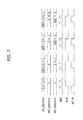
- FIG. 7 is a timing diagram illustrating an operation of the memory device of FIG. 1 . More specifically, FIG. 7 illustrates the operation of a memory device employing the detection counter 130 of FIG. 3 , according to an embodiment of the invention.
- the counting addresses CNT_ADD ⁇ 0:9>, the row detection addresses DET_RADD ⁇ 0:9>, and the column detection addresses DET_CADD ⁇ 0:4> are expressed by decimal numbers.
- all the counting addresses CNT_ADD ⁇ 0:9>, the row detection addresses DET_RADD ⁇ 0:9>, and the column detection addresses DET_CADD ⁇ 0:4> are 0 in an initial state.
- the flag signal FLAG is low in an initial state.
- the detection period signal DET_OP becomes high.
- the detection period signal DET_OP may become low, so that no detection operation is performed even though the refresh signal REFA is activated.
- the detection period signal DET_OP becomes high.
- the column detection addresses DET_CADD ⁇ 0:4> may be increased from 0 to 1.
Landscapes
- Engineering & Computer Science (AREA)
- Microelectronics & Electronic Packaging (AREA)
- Computer Hardware Design (AREA)
- Theoretical Computer Science (AREA)
- Dram (AREA)
- Quality & Reliability (AREA)
- Physics & Mathematics (AREA)
- General Engineering & Computer Science (AREA)
- General Physics & Mathematics (AREA)
- Health & Medical Sciences (AREA)
- Biomedical Technology (AREA)
- For Increasing The Reliability Of Semiconductor Memories (AREA)
Abstract
Description
Claims (16)
Applications Claiming Priority (2)
| Application Number | Priority Date | Filing Date | Title |
|---|---|---|---|
| KR10-2015-0127462 | 2015-09-09 | ||
| KR1020150127462A KR20170030675A (en) | 2015-09-09 | 2015-09-09 | Memory device |
Publications (2)
| Publication Number | Publication Date |
|---|---|
| US20170068583A1 US20170068583A1 (en) | 2017-03-09 |
| US10014071B2 true US10014071B2 (en) | 2018-07-03 |
Family
ID=58189441
Family Applications (1)
| Application Number | Title | Priority Date | Filing Date |
|---|---|---|---|
| US15/066,773 Active 2036-08-16 US10014071B2 (en) | 2015-09-09 | 2016-03-10 | Comparing twice-read memory cell data for error detection in a memory device |
Country Status (2)
| Country | Link |
|---|---|
| US (1) | US10014071B2 (en) |
| KR (1) | KR20170030675A (en) |
Families Citing this family (1)
| Publication number | Priority date | Publication date | Assignee | Title |
|---|---|---|---|---|
| US10836400B2 (en) * | 2017-12-19 | 2020-11-17 | Micron Technology, Inc. | Implementing safety measures in applications |
Citations (5)
| Publication number | Priority date | Publication date | Assignee | Title |
|---|---|---|---|---|
| US7397719B2 (en) * | 2005-05-12 | 2008-07-08 | Nec Electronics Corporation | Volatile semiconductor memory |
| US20080215939A1 (en) * | 2007-02-08 | 2008-09-04 | Samsung Electronics Co., Ltd. | Semiconductor memory device with fail-bit storage unit and method for parallel bit testing |
| US8289770B2 (en) * | 2008-09-12 | 2012-10-16 | Samsung Electronics Co., Ltd. | Semiconductor memory device and system including the same |
| KR20130117198A (en) | 2012-04-18 | 2013-10-25 | 삼성전자주식회사 | A method refreshing memory cells and a semiconductor memory device using thereof |
| US20170052840A1 (en) * | 2015-08-19 | 2017-02-23 | SK Hynix Inc. | Memory device and operating method thereof |
-
2015
- 2015-09-09 KR KR1020150127462A patent/KR20170030675A/en not_active Withdrawn
-
2016
- 2016-03-10 US US15/066,773 patent/US10014071B2/en active Active
Patent Citations (6)
| Publication number | Priority date | Publication date | Assignee | Title |
|---|---|---|---|---|
| US7397719B2 (en) * | 2005-05-12 | 2008-07-08 | Nec Electronics Corporation | Volatile semiconductor memory |
| US20080215939A1 (en) * | 2007-02-08 | 2008-09-04 | Samsung Electronics Co., Ltd. | Semiconductor memory device with fail-bit storage unit and method for parallel bit testing |
| US8289770B2 (en) * | 2008-09-12 | 2012-10-16 | Samsung Electronics Co., Ltd. | Semiconductor memory device and system including the same |
| KR20130117198A (en) | 2012-04-18 | 2013-10-25 | 삼성전자주식회사 | A method refreshing memory cells and a semiconductor memory device using thereof |
| US20170052840A1 (en) * | 2015-08-19 | 2017-02-23 | SK Hynix Inc. | Memory device and operating method thereof |
| KR20170023249A (en) | 2015-08-19 | 2017-03-03 | 에스케이하이닉스 주식회사 | Memory device and method operating for memory device |
Also Published As
| Publication number | Publication date |
|---|---|
| US20170068583A1 (en) | 2017-03-09 |
| KR20170030675A (en) | 2017-03-20 |
Similar Documents
| Publication | Publication Date | Title |
|---|---|---|
| US10867660B2 (en) | Apparatus and methods for controlling refresh operations | |
| US10020073B2 (en) | Memory device and operating method thereof | |
| US8379471B2 (en) | Refresh operation control circuit, semiconductor memory device including the same, and refresh operation control method | |
| US10614873B2 (en) | Memory device, memory system including the same, and address counting and comparing operation for refresh operation method thereof | |
| US9190139B2 (en) | Memory and memory system including the same | |
| US9165634B2 (en) | Semiconductor memory device and refresh control system | |
| CN104376868B (en) | Memory and storage system including it | |
| CN105321550B (en) | Memory device | |
| US9123447B2 (en) | Memory, memory system including the same and method for operating memory | |
| US9672892B2 (en) | Memory device and memory system including the same | |
| US9514798B2 (en) | Address storage circuit and memory and memory system including the same | |
| CN106816180B (en) | Memory device and method of operation | |
| US20180122454A1 (en) | Address counting circuit, memory device and operating method thereof | |
| US10043569B2 (en) | Memory device for detecting failure of memory cells and refreshing memory cells | |
| US9818491B2 (en) | Memory device and operating method thereof | |
| US9922728B2 (en) | Memory device | |
| US10014071B2 (en) | Comparing twice-read memory cell data for error detection in a memory device | |
| US10255966B2 (en) | Memory device and operating method thereof | |
| US12046270B2 (en) | Memory and operation method of the same | |
| US20230317200A1 (en) | Error handling device, semiconductor memory device including the same, and error handliing method |
Legal Events
| Date | Code | Title | Description |
|---|---|---|---|
| AS | Assignment |
Owner name: SK HYNIX INC., KOREA, REPUBLIC OF Free format text: ASSIGNMENT OF ASSIGNORS INTEREST;ASSIGNORS:PARK, MIN-SU;KIM, JAE-IL;KIM, TAE-KYUN;AND OTHERS;REEL/FRAME:038058/0617 Effective date: 20160224 |
|
| STCF | Information on status: patent grant |
Free format text: PATENTED CASE |
|
| MAFP | Maintenance fee payment |
Free format text: PAYMENT OF MAINTENANCE FEE, 4TH YEAR, LARGE ENTITY (ORIGINAL EVENT CODE: M1551); ENTITY STATUS OF PATENT OWNER: LARGE ENTITY Year of fee payment: 4 |
|
| AS | Assignment |
Owner name: MIMIRIP LLC, TEXAS Free format text: ASSIGNMENT OF ASSIGNORS INTEREST;ASSIGNOR:SK HYNIX INC.;REEL/FRAME:067335/0246 Effective date: 20240311 Owner name: MIMIRIP LLC, TEXAS Free format text: ASSIGNMENT OF ASSIGNOR'S INTEREST;ASSIGNOR:SK HYNIX INC.;REEL/FRAME:067335/0246 Effective date: 20240311 |
|
| MAFP | Maintenance fee payment |
Free format text: PAYMENT OF MAINTENANCE FEE, 8TH YEAR, LARGE ENTITY (ORIGINAL EVENT CODE: M1552); ENTITY STATUS OF PATENT OWNER: LARGE ENTITY Year of fee payment: 8 |