US10003184B2 - Backflow preventing device, power conversion device, and refrigeration air-conditioning apparatus - Google Patents
Backflow preventing device, power conversion device, and refrigeration air-conditioning apparatus Download PDFInfo
- Publication number
- US10003184B2 US10003184B2 US14/780,036 US201414780036A US10003184B2 US 10003184 B2 US10003184 B2 US 10003184B2 US 201414780036 A US201414780036 A US 201414780036A US 10003184 B2 US10003184 B2 US 10003184B2
- Authority
- US
- United States
- Prior art keywords
- commutation
- backflow preventing
- current
- power source
- load
- Prior art date
- Legal status (The legal status is an assumption and is not a legal conclusion. Google has not performed a legal analysis and makes no representation as to the accuracy of the status listed.)
- Active, expires
Links
Images


Classifications
-
- H—ELECTRICITY
- H02—GENERATION; CONVERSION OR DISTRIBUTION OF ELECTRIC POWER
- H02H—EMERGENCY PROTECTIVE CIRCUIT ARRANGEMENTS
- H02H3/00—Emergency protective circuit arrangements for automatic disconnection directly responsive to an undesired change from normal electric working condition with or without subsequent reconnection ; integrated protection
- H02H3/003—Emergency protective circuit arrangements for automatic disconnection directly responsive to an undesired change from normal electric working condition with or without subsequent reconnection ; integrated protection responsive to reversal of power transmission direction
-
- H—ELECTRICITY
- H02—GENERATION; CONVERSION OR DISTRIBUTION OF ELECTRIC POWER
- H02M—APPARATUS FOR CONVERSION BETWEEN AC AND AC, BETWEEN AC AND DC, OR BETWEEN DC AND DC, AND FOR USE WITH MAINS OR SIMILAR POWER SUPPLY SYSTEMS; CONVERSION OF DC OR AC INPUT POWER INTO SURGE OUTPUT POWER; CONTROL OR REGULATION THEREOF
- H02M3/00—Conversion of DC power input into DC power output
- H02M3/02—Conversion of DC power input into DC power output without intermediate conversion into AC
- H02M3/04—Conversion of DC power input into DC power output without intermediate conversion into AC by static converters
- H02M3/10—Conversion of DC power input into DC power output without intermediate conversion into AC by static converters using discharge tubes with control electrode or semiconductor devices with control electrode
- H02M3/145—Conversion of DC power input into DC power output without intermediate conversion into AC by static converters using discharge tubes with control electrode or semiconductor devices with control electrode using devices of a triode or transistor type requiring continuous application of a control signal
- H02M3/155—Conversion of DC power input into DC power output without intermediate conversion into AC by static converters using discharge tubes with control electrode or semiconductor devices with control electrode using devices of a triode or transistor type requiring continuous application of a control signal using semiconductor devices only
- H02M3/156—Conversion of DC power input into DC power output without intermediate conversion into AC by static converters using discharge tubes with control electrode or semiconductor devices with control electrode using devices of a triode or transistor type requiring continuous application of a control signal using semiconductor devices only with automatic control of output voltage or current, e.g. switching regulators
- H02M3/158—Conversion of DC power input into DC power output without intermediate conversion into AC by static converters using discharge tubes with control electrode or semiconductor devices with control electrode using devices of a triode or transistor type requiring continuous application of a control signal using semiconductor devices only with automatic control of output voltage or current, e.g. switching regulators including plural semiconductor devices as final control devices for a single load
-
- H—ELECTRICITY
- H02—GENERATION; CONVERSION OR DISTRIBUTION OF ELECTRIC POWER
- H02M—APPARATUS FOR CONVERSION BETWEEN AC AND AC, BETWEEN AC AND DC, OR BETWEEN DC AND DC, AND FOR USE WITH MAINS OR SIMILAR POWER SUPPLY SYSTEMS; CONVERSION OF DC OR AC INPUT POWER INTO SURGE OUTPUT POWER; CONTROL OR REGULATION THEREOF
- H02M1/00—Details of apparatus for conversion
- H02M1/0048—Circuits or arrangements for reducing losses
- H02M1/0051—Diode reverse recovery losses
-
- H—ELECTRICITY
- H02—GENERATION; CONVERSION OR DISTRIBUTION OF ELECTRIC POWER
- H02M—APPARATUS FOR CONVERSION BETWEEN AC AND AC, BETWEEN AC AND DC, OR BETWEEN DC AND DC, AND FOR USE WITH MAINS OR SIMILAR POWER SUPPLY SYSTEMS; CONVERSION OF DC OR AC INPUT POWER INTO SURGE OUTPUT POWER; CONTROL OR REGULATION THEREOF
- H02M1/00—Details of apparatus for conversion
- H02M1/32—Means for protecting converters other than automatic disconnection
- H02M1/34—Snubber circuits
- H02M1/342—Active non-dissipative snubbers
-
- H—ELECTRICITY
- H02—GENERATION; CONVERSION OR DISTRIBUTION OF ELECTRIC POWER
- H02M—APPARATUS FOR CONVERSION BETWEEN AC AND AC, BETWEEN AC AND DC, OR BETWEEN DC AND DC, AND FOR USE WITH MAINS OR SIMILAR POWER SUPPLY SYSTEMS; CONVERSION OF DC OR AC INPUT POWER INTO SURGE OUTPUT POWER; CONTROL OR REGULATION THEREOF
- H02M1/00—Details of apparatus for conversion
- H02M1/42—Circuits or arrangements for compensating for or adjusting power factor in converters or inverters
- H02M1/4208—Arrangements for improving power factor of AC input
- H02M1/4225—Arrangements for improving power factor of AC input using a non-isolated boost converter
-
- H02M2001/0051—
-
- H02M2001/342—
-
- Y—GENERAL TAGGING OF NEW TECHNOLOGICAL DEVELOPMENTS; GENERAL TAGGING OF CROSS-SECTIONAL TECHNOLOGIES SPANNING OVER SEVERAL SECTIONS OF THE IPC; TECHNICAL SUBJECTS COVERED BY FORMER USPC CROSS-REFERENCE ART COLLECTIONS [XRACs] AND DIGESTS
- Y02—TECHNOLOGIES OR APPLICATIONS FOR MITIGATION OR ADAPTATION AGAINST CLIMATE CHANGE
- Y02B—CLIMATE CHANGE MITIGATION TECHNOLOGIES RELATED TO BUILDINGS, e.g. HOUSING, HOUSE APPLIANCES OR RELATED END-USER APPLICATIONS
- Y02B70/00—Technologies for an efficient end-user side electric power management and consumption
- Y02B70/10—Technologies improving the efficiency by using switched-mode power supplies [SMPS], i.e. efficient power electronics conversion e.g. power factor correction or reduction of losses in power supplies or efficient standby modes
-
- Y02B70/126—
-
- Y02B70/1491—
Definitions
- the present invention relates to, for example, a backflow preventing device included in a power conversion device and other apparatus.
- variable voltage variable frequency inverter devices Along with increased practical uses of variable voltage variable frequency inverter devices and other devices, application fields of various kinds of power conversion device have been developed.
- Patent Literature 1 Japanese Unexamined Patent Application Publication No. 2005-160284 (FIG. 1)
- the present invention has been made in view of the above-mentioned problem, and provides a backflow preventing device and the like, which are capable of securing high efficiency, high reliability, and others.
- the present invention is also aimed at further reducing a loss due to power conversion.
- a backflow preventing device including a backflow preventing element connected between a power source and a load, for preventing a backflow of a current from the load side to the power source side, a commutation device for performing a commutation operation of causing a current to flow through an other path connected in parallel to the backflow preventing element, and a controller configured to determine a time period for performing the commutation operation, and control the commutation device to perform the commutation operation based on the determined time period.
- the commutation device capable of performing the commutation operation is provided, and hence a current attempting to flow through the backflow preventing element may be commutated to the other path, to thereby reduce a recovery current generated in the backflow preventing element when the current flows reversely from the load side. Consequently, a reduction in loss, a reduction in level of noise terminal voltage, measures for EMC, and other advantages may be achieved to increase the efficiency in the system as a whole.
- the time period for performing the commutation operation is determined, and then the commutation device is controlled to perform the commutation operation, and hence the commutation operation may be performed only for a time period necessary for the commutation operation. Consequently, electric power relating to the commutation operation not contributing to power conversion may be reduced to save energy.
- FIG. 1 is a diagram illustrating a system configuration mainly including a power conversion device according to Embodiment 1 of the present invention.
- FIG. 2 is a diagram (first example) illustrating a configuration of a power source 1 .
- FIG. 3 is a diagram (second example) illustrating a configuration of the power source 1 .
- FIG. 4 is a diagram (third example) illustrating a configuration of the power source 1 .
- FIG. 5 is a diagram illustrating an example of a configuration in which a commutation device 7 is connected in parallel to a backflow preventing element 5 according to Embodiment 1 of the present invention.
- FIG. 6 is a diagram illustrating an example of a block configuration of control functions of a controller 100 according to Embodiment 1 of the present invention.
- FIG. 7 is a diagram illustrating an example (first example) of a current path according to Embodiment 1 of the present invention.
- FIG. 8 is a diagram illustrating an example (second example) of the current path according to Embodiment 1 of the present invention.
- FIG. 9 is a diagram illustrating an example (third example) of the current path according to Embodiment 1 of the present invention.
- FIG. 10 is a diagram illustrating the waveforms of signals and currents at the time when the commutation device 7 is operated according to Embodiment 1 of the present invention.
- FIG. 11 is a diagram illustrating an example of the waveforms of signals and currents at the time when the commutation device 7 is operated according to Embodiment 1 of the present invention.
- FIG. 12 is a diagram illustrating another example of the configuration of the system and the like mainly including the power conversion device according to Embodiment 1 of the present invention.
- FIG. 13 is a diagram illustrating voltages obtained when an AC power source is used for a power source 1 .
- FIG. 14 is a diagram illustrating an example of the waveforms of signals and currents at the time when a power source phase is A and C of FIG. 9 according to Embodiment 1 of the present invention.
- FIG. 15 is a diagram illustrating an example of the waveforms of signals and currents at the time when the power source phase is B and D of FIG. 9 according to Embodiment 1 of the present invention.
- FIG. 16 is a diagram illustrating the waveforms of signals and currents at the time when the commutation device 7 is operated according to Embodiment 2 of the present invention.
- FIG. 17 is a diagram illustrating the waveforms of signals and currents at the time when the commutation device 7 is operated according to Embodiment 3 of the present invention.
- FIG. 18 is a diagram illustrating the waveforms of signals and currents at the time when the commutation device 7 is operated according to Embodiment 4 of the present invention.
- FIG. 19 is a diagram illustrating an example of the configuration of the system and the like mainly including the power conversion device according to Embodiment 7 of the present invention.
- FIG. 20 is a configuration diagram of a refrigeration air-conditioning apparatus according to Embodiment 9 of the present invention.
- FIG. 1 is a diagram illustrating an example of a system configuration and other configurations mainly including a power conversion device according to Embodiment 1 of the present invention. First, a description is given of the system configuration illustrated in FIG. 1 including the power conversion device capable of performing highly efficient power conversion.
- the power conversion device is provided between a power source 1 and a load 9 , and converts electric power from the power source 1 to supply the converted electric power to the load 9 .
- the power conversion device in this embodiment performs boosting, and includes, for example, a chopper circuit 6 , a commutation device 7 , and a smoothing device 8 .
- FIG. 2 to FIG. 4 are diagrams illustrating configurations of the power source 1 .
- FIG. 2 is a diagram of the power source 1 constructed with a DC power source 1 A.
- FIG. 3 is a diagram of the power source 1 constructed with a single-phase AC power source 1 B and a rectification circuit (rectification device) 2 B.
- FIG. 4 is a diagram of the power source 1 constructed with a three-phase AC power source 1 C and a rectification circuit (rectification device) 2 C.
- Each of the rectification circuits 2 B and 2 C is constructed with bridge-connected rectification elements such as diodes, and rectifies electric power supplied from the power source 1 . In this manner, the power conversion device in this embodiment can deal with various types of the power source 1 .
- the chopper circuit 6 includes a reactor 3 , a short-circuit device (switch device) 4 , and a backflow preventing element 5 .
- the reactor 3 is connected on the power source 1 side, and is provided to suppress harmonic waves.
- the short-circuit device 4 includes a switching element, such as an insulated gate bipolar transistor (IGBT).
- IGBT insulated gate bipolar transistor
- the backflow preventing element 5 is an element for preventing the backflow of a current supplied from the smoothing device 8 between the short-circuit device 4 and the smoothing device 8 .
- the backflow preventing element 5 is a semiconductor element as exemplified by a fast recovery diode, which has excellent electrical characteristics (in particular, recovery characteristics), has a small current capacity, and takes a short time to complete reverse recovery.
- the commutation device 7 is a device connected in parallel to the backflow preventing element 5 . Then, the commutation device 7 commutates the current flowing through the backflow preventing element 5 to a different path (path not via the backflow preventing element 5 ) at a necessary timing.
- the backflow preventing element 5 and the commutation device 7 construct a backflow preventing device for preventing the backflow of the current from the load 9 side to the power source 1 side.
- FIG. 5 is a diagram illustrating an example of the configuration in which the commutation device 7 is connected in parallel to the backflow preventing element 5 according to Embodiment 1 of the present invention.
- the commutation device 7 includes, for example, a transformer 71 , a commutation rectification element 72 such as a diode connected in series to a secondary-side winding of the transformer 71 , and a transformer drive circuit 73 for operating the transformer 71 .
- the transformer drive circuit 73 includes, for example, a commutation power source 75 for supplying electric power to the transformer 71 , and a commutation switch 74 , which is configured to be opened or closed based on a drive signal (commutation drive signal) transmitted from the controller 100 , for controlling the supply of electric power to the transformer 71 (primary-side winding) and the stop of the supply.
- the commutation rectification element 72 is also constructed with a semiconductor element as exemplified by a fast recovery diode.
- a Schottky barrier diode having good recovery characteristics, a low forward voltage, and a high breakdown voltage with a small loss may be used.
- a wide band-gap semiconductor element containing silicon carbide (SiC), gallium nitride (GaN), or diamond as its material may be used.
- SiC silicon carbide
- GaN gallium nitride
- diamond diamond as its material.
- the backflow preventing element 5 , the secondary-side winding of the transformer 71 , and the commutation rectification element 72 can be insulated from the transformer drive circuit 73 and the controller 100 because the transformer 71 is interposed therebetween. Consequently, a signal for driving the commutation device 7 can be injected relatively easily. Further, the system with high safety and high reliability can be constructed.
- FIG. 5 the example in which the secondary-side winding of the transformer 71 and the anode side of the commutation rectification element 72 are connected to each other is illustrated, but the present invention is not limited to such connection as long as the direction of a current flowing through the commutation rectification element 72 is not changed.
- the cathode side of the commutation rectification element 72 may be connected to the secondary-side winding of the transformer 71 .
- the transformer drive circuit 73 is constructed with the commutation switch 74 and the commutation power source 75 , but a limiting resistor, a high frequency capacitor, a snubber circuit, a protective circuit, or other circuits may be inserted as necessary into the electrical circuit constructed with the commutation power source 75 , the commutation switch 74 , and the primary-side winding of the transformer 71 in consideration of noise countermeasures and protection in case of failure.
- a reset winding may be added as necessary to the primary-side winding of the transformer 71 to reset an excitation current.
- a rectifier or other circuits may be provided so that excitation energy may be regenerated on the power source side to increase the efficiency.
- the smoothing device 8 is constructed with use of a capacitor, for example.
- the smoothing device 8 smoothes a voltage applied from the power source 1 , and applies a DC voltage (output voltage, bus voltage) to the load 9 to supply electric power to the load 9 .
- the load 9 is driven with the electric power supplied via the smoothing device 8 .
- a load voltage detection unit 101 is a voltage detector for detecting the voltage smoothed by the smoothing device 8 and applied to the load 9 , and outputting a voltage detection value as a detection signal.
- a current detection unit 102 is a current detector for detecting a current (bus current) flowing from the power source 1 , and outputting a current detection value as a detection signal. A current flowing through the reactor 3 can be detected based also on the current detection value of the current detection unit 102 .
- a power source voltage detection unit 103 is a voltage detector for detecting the voltage applied from the power source 1 , and outputting a voltage detection value as a detection signal.
- the controller 100 is a device for performing processing of calculating an operating time period (short-circuit time period) of the short-circuit device 4 , the commutation device 7 , and other devices based on the detection signals of the load voltage detection unit 101 , the current detection unit 102 , and the power source voltage detection unit 103 .
- the controller 100 includes an arithmetic unit such as a microcomputer and a digital signal processor including a processing device such as a CPU, a storage device, and other components, or a device having an internal function similar to the arithmetic unit.
- FIG. 6 is a diagram illustrating an example of a block configuration of control functions of the controller 100 according to Embodiment 1 of the present invention.
- an on-duty calculation unit 100 A calculates an on-duty of the short-circuit device 4 based on, for example, a voltage detection value and a load voltage command value relating to the detection by the load voltage detection unit 101 , and transmits an output signal (on-duty signal).
- the on-duty calculation unit 100 A calculates the on-duty based on the voltage detection value and the load voltage command value relating to the detection by the load voltage detection unit 101 , but the present invention is not limited thereto.
- the on-duty calculation unit 100 A may calculate the on-duty based on a current detection value and a current command value relating to the detection by the current detection unit 102 .
- the on-duty calculation unit 100 A may calculate the on-duty based on a voltage detection value and a load voltage command value relating to the detection by the power source voltage detection unit 103 .
- the on-duty calculation unit 100 A may calculate the on-duty based on a combination of the respective values relating to the current and the voltage.
- a drive signal generation unit 100 B generates drive signals for the short-circuit device 4 and the commutation device 7 based on the output signal from the on-duty calculation unit 100 A, and transmits the generated drive signals to the short-circuit device 4 and the commutation device 7 , respectively.
- the power conversion device in this embodiment adds the commutation operation of the commutation device 7 to a power conversion operation of a DC chopper, for example. In this manner, the backflow preventing element 5 performs reverse recovery before the current flows reversely from the smoothing device 8 , to thereby reduce a recovery current.
- FIG. 7 to FIG. 9 are diagrams illustrating examples of the current path according to Embodiment 1 of the present invention.
- FIG. 7 to FIG. 9 are illustrations of the paths in representative operation examples among the combination of the open/close states of the short-circuit device 4 and the commutation switch 74 included in the commutation device 7 .
- the power source 1 is constructed with the combination of the single-phase AC power source 1 B and the rectification circuit 2 B as illustrated in FIG. 3 .
- the rectification circuit is constructed with rectification elements 2 a to 2 d.
- FIG. 7 is an illustration of the state in which the short-circuit device 4 is off (opened) and the commutation switch 74 is off.
- the formed circuit is equivalent to a simple full-wave rectification circuit.
- one of the terminals of the power source 1 connected to the rectification elements 2 a and 2 b has a higher potential, the current path is formed from the power source 1 to the rectification element 2 d via the rectification element 2 a , the reactor 3 , the backflow preventing element 5 , and the load 9 in the stated order.
- FIG. 8 is an illustration of the state in which the short-circuit device 4 is on (closed) and the commutation switch 74 is off.
- a short-circuit current flows through the path from the power source 1 to the rectification element 2 d via the rectification element 2 a , the reactor 3 , and the short-circuit device 4 in the stated order.
- the voltage applied to the reactor 3 is substantially the same as the voltage of the power source 1 .
- the section in which the smoothing device 8 is discharged to cause a current to flow through the load 9 has a section in which the input current of the power source 1 is disconnected.
- the short-circuit device 4 when the short-circuit device 4 is turned on, the short-circuit current flows via the reactor 3 as illustrated in FIG. 8 , and hence the input current of the power source 1 flows even in the current-disconnected section as described above. Accordingly, when the short-circuit device 4 is repeatedly switched on and off, the current paths illustrated in FIG. 7 and FIG. 8 can be repeatedly formed.
- the waveform of the input current of the power source 1 can be arbitrarily changed to improve the power factor and the rate of content of a harmonic current.
- a rectifier diode has a tendency that the amount of stored carriers increases as the current capacity increases. Accordingly, when the current capacity increases, the recovery current also increases. Further, the recovery current increases as the applied reverse bias voltage becomes higher.
- the reverse recovery is not performed in a manner that a high reverse bias voltage is applied to the backflow preventing element 5 having a large current capacity, but control is performed so that the reverse recovery may be performed in a manner that the commutation path is formed by the commutation device 7 and a low reverse bias voltage is applied to the backflow preventing element 5 via the transformer 71 and the commutation rectification element 72 immediately before the short-circuit device 4 is turned on (hereinafter this control is referred to as “commutation control”).
- FIG. 9 is an illustration of the state in which the short-circuit device 4 is off and the commutation switch 74 is on.
- the current path in this case is formed from the power source 1 to the rectification element 2 d via the rectification element 2 a , the reactor 3 , the backflow preventing element 5 , and the load 9 in the stated order similarly to FIG. 7 .
- the commutation switch 74 is turned on, and hence the transformer 71 is excited, and the current flows also into the path from the secondary-side winding of the transformer 71 to the commutation rectification element 72 of the commutation device 7 . Then, after a predetermined period of time has elapsed, the current is completely commutated to the path on the commutation rectification element 72 side.
- FIG. 10 is a diagram illustrating the waveforms of signals and currents at the time when the commutation device 7 is operated according to Embodiment 1 of the present invention.
- the HI side is the active direction (on direction).
- the drive signal for the commutation device 7 is turned on immediately before the drive signal for the short-circuit device 4 is turned on. In this case, the current starts to flow through the path of the secondary-side winding of the transformer 71 due to the excitation current.
- the current starts to flow while branching into the respective directions of the backflow preventing element 5 and the commutation rectification element 72 .
- the current no longer flows to the backflow preventing element 5 , and all the currents flow to the commutation rectification element 72 side (the commutation is completed).
- the commutation power source 75 included in the transformer drive circuit 73 is set to have a value sufficiently smaller than the output voltage of the smoothing device 8 .
- the backflow preventing element 5 can be turned off (reverse recovery) with a low reverse bias voltage.
- the reverse recovery operation of the commutation rectification element 72 is performed, and also in this case, the recovery current is generated.
- the current supply period for the commutation rectification element 72 is significantly shorter than that for the backflow preventing element 5 . Accordingly, the effective current flowing through the commutation rectification element 72 is small, and hence the required current capacity can be reduced.
- the recovery current can be reduced as compared to the case where the recovery current is generated by the backflow preventing element 5 (note that, an element is selected in consideration of the peak current).
- the noise amount and loss caused by the recovery current can be reduced in the system as a whole. In this manner, the level of noise terminal voltage and radiation noise is reduced, and the circuit loss is suppressed. Consequently, a noise filter can be downsized to reduce the cost.
- any one of a drive power source (gate drive power source (not shown)) for operating the short-circuit device 4 and a power source (not shown) for the controller 100 can be shared with the commutation power source 75 of the transformer drive circuit 73 . Consequently, it is not necessary to generate an additional power source, and the increase in cost can be avoided.
- the recovery current in the backflow preventing element 5 can be reduced to reduce the loss, to thereby perform power conversion and the like with higher efficiency in the system as a whole.
- the commutation operation of the commutation device 7 and the excitation operation for performing the commutation operation do not directly contribute to the power conversion performed by the power conversion device, but are the loss.
- the electric power relating to the commutation operation becomes smaller to increase the efficiency and save more energy.
- the electric power relating to the commutation operation can be reduced in a manner that the commutation operation and the excitation operation are performed only for a time period required for the commutation operation.
- FIG. 11 is a diagram illustrating an example of the waveforms of signals and currents at the time when the commutation device 7 is operated according to Embodiment 1 of the present invention.
- the time period during which the commutation operation is performed is the time period during which the current flows through the commutation rectification element 72 (time period represented by a commutation pulse width TD 1 ).
- the time period of the commutation operation can be shortened in a manner that the commutation pulse width TD 1 is reduced.
- the controller 100 only needs to transmit the commutation drive signal having the pulse width TD 2 to the commutation device 7 so that the current of the commutation pulse width TD 1 may flow for the time period required for the commutation operation.
- the current (reactor current) Idc_ 0 ( n ) flowing through the reactor 3 is calculated to determine the minimum value (minimum time period) of the commutation pulse width TD 1 , which is the minimum time period required for the commutation operation.
- Idc_ 0 ( n ) corresponds to the valley of the reactor current as illustrated in FIG. 11 , and is the minimum current required to perform the commutation operation.
- the reactor current Idc_ 0 ( n ) is calculated in this case, but it is more preferred to use a current with which the current flowing through the backflow preventing element 5 in the commutation operation can be detected or estimated.
- the controller 100 calculates Idc_ 0 ( n ).
- the procedure of calculating Idc_ 0 ( n ) differs depending on the timing of acquiring the current detection value of the current detection unit 102 .
- the controller 100 calculates the current detection value Idc(n) based on Expression (1).
- Ton represents the on period of the short-circuit device 4
- Toff represents the off period of the short-circuit device 4 .
- the controller 100 calculates the current detection value Idc(n) based on Expression (2).
- Idc _0( n ) Idc ( n ) +kb ⁇ T off (2)
- the minimum width of the commutation pulse width TD 1 can be calculated by Expression (3).
- Lcc represents leakage inductance in the secondary-side winding of the transformer 71 .
- FIG. 12 is a diagram illustrating another example of a system configuration and other configurations mainly including a power conversion device according to Embodiment 1 of the present invention.
- the devices denoted by the same reference symbols as those in FIG. 1 perform the same operations and the like as those described in Embodiment 1.
- the voltage Vdc expressed in Expression (3) can use a voltage detection value relating to the detection by the load voltage detection unit 101 .
- the voltage Vdc may be calculated based on a voltage command value and other values input to the controller 100 .
- the voltage Vdc is used in this case, but it is more preferred to use a voltage with which the voltage (inter-terminal voltage) applied to the backflow preventing element 5 can be detected or estimated.
- a detection method therefor for example, as illustrated in FIG. 12 , an inter-terminal voltage detection unit 105 is connected to detect the inter-terminal voltage of the backflow preventing element 5 .
- the leakage inductance Lcc may be stored in, for example, a storage device included in the controller 100 as numerical data in advance.
- the numerical value that takes the ratio of the leakage inductance to the inductance of a general transformer (for example, 0.1 of the inductance of the transformer) into consideration may be stored as the data.
- the leakage inductance Lcc changes depending on the temperature, the current, or other parameters, data in the form of a table may be prepared, and a numerical value may be selected based on the temperature, the current, or other parameters at the time of calculation.
- the leakage inductance Lcc is used in this case, but it is more preferred to use an inductance with which the increase rate of the current flowing through the commutation device 7 in the commutation operation can be detected or estimated.
- the margin a may be adjusted depending on the switching speed when the switching speed is variable depending on the load 9 or other devices.
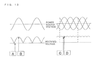
- FIG. 13 is a diagram illustrating the voltages obtained when an AC power source is used for the power source 1 . As illustrated in FIG. 13 , when the power source 1 is a combination of an AC power source and a rectification circuit, the rectified voltage value differs depending on the power source phase.
- FIG. 14 is a diagram illustrating an example of the waveforms of the signals and the currents at the time when the power source phase is A and C of FIG. 13 according to Embodiment 1 of the present invention.
- the power source phase is A and C illustrated in FIG. 13
- the chopper circuit 6 is operated to improve the power factor
- the current flowing is reduced as illustrated in FIG. 14 .
- the recovery current flowing through the backflow preventing element 5 is reduced.
- FIG. 15 is a diagram illustrating an example of the waveforms of the signals and the currents at the time when the power source phase is B and D of FIG. 13 according to Embodiment 1 of the present invention.
- the current flowing is increased as illustrated in FIG. 15 .
- the recovery current flowing through the backflow preventing element 5 is increased.
- the boost ratio is large when the rectified voltage value is small, and the boost ratio is small when the rectified voltage value is large.
- the boost ratio changes irrespective of the power source phase, such as when the load voltage command value is changed or when the rectified voltage value fluctuates due to fluctuations in power source voltage.
- Idc_ 0 ( n ) reduces to reduce the recovery current flowing through the backflow preventing element 5 .
- the relationship between the boost ratio and the recovery current changes with a tendency opposite to that in the case described with reference to FIG. 13 , FIG. 14 , and FIG. 15 .
- the margin may be set in consideration of the fact that the boost ratio, the power source phase ( 2 f for a single-phase power source, 6 f for a three-phase power source) when the AC power source is used, the fluctuations in power source voltage, and other parameters differ as described above. Further, the margin a may be changed depending on the operation conditions of the device.
- the controller 100 transmits the commutation drive signal having the thus determined pulse width TD 2 to the commutation device 7 , to thereby control the commutation device 7 to perform the commutation operation.
- the reactor current and other parameters are calculated to calculate the minimum width of the commutation pulse width TD 1 , and the commutation drive signal is transmitted correspondingly to the minimum width, to thereby control the commutation device 7 to perform the commutation operation. Consequently, the time period for performing the commutation operation can be reduced as much as possible, and the electric power relating to the commutation operation not contributing to power conversion can be reduced to save the energy.
- FIG. 16 is a diagram illustrating another example of the waveforms of signals and currents at the time when the commutation device 7 is operated according to Embodiment 2 of the present invention.
- the current (reactor current) Idc_ 0 ( n ) flowing through the reactor 3 is calculated as the current with which the current flowing through the backflow preventing element 5 in the commutation operation can be detected or estimated.
- the reactor current Idc_ 0 ( n ) is calculated based on the short-circuit current (switching current) flowing through the short-circuit device 4 .
- Idc_ 0 ( n ) when the controller 100 acquires the switching current as the current detection value Idc(n) in synchronization with the valley of the carrier signal, Idc_ 0 ( n ) can be calculated based on Expression (1).
- the controller 100 can calculate the reactor current Idc_ 0 ( n ) based on the switching current flowing through the short-circuit device 4 in the period during which the short-circuit device 4 is on.
- FIG. 17 is a diagram illustrating another example of the waveforms of signals and currents at the time when the commutation device 7 is operated according to Embodiment 3 of the present invention.
- the reactor current Idc_ 0 ( n ) is calculated based on the current (element current) flowing through the backflow preventing element 5 in the commutation operation.
- the element current is zero (does not flow).
- Idc_ 0 ( n ) when the controller 100 acquires the switching current as the current detection value Idc(n) in synchronization with the peak of the carrier signal, Idc_ 0 ( n ) can be calculated based on Expression (2).
- the controller 100 can calculate the reactor current Idc_ 0 ( n ) based on the element current flowing through the backflow preventing element 5 at the time of commutation operation in the period during which the short-circuit device 4 is off.
- FIG. 18 is a diagram illustrating another example of the waveforms of signals and currents at the time when the commutation device 7 is operated according to Embodiment 4 of the present invention.
- the reactor current Idc_ 0 ( n ) is calculated based on a current (power source current) from the power source 1 formed of a combination of an AC power source and a rectification circuit.
- a current power source current
- the reactor current can be known based on the power source current, and hence the reactor current Idc_ 0 ( n ) can be calculated based on Expression (1) or Expression (2).
- an upper limit value and a lower limit value which can be determined, may be set for the commutation pulse width TD 1 or the pulse width TD 2 (time period for performing the commutation operation) determined by calculation, for example.
- the recovery loss at the time when the commutation operation is not performed is smaller than the loss (electric power) generated when the commutation operation is performed, it is not necessary to perform the commutation operation.
- such a pulse width that the same loss as the recovery loss at the time when the commutation operation is not performed is generated may be set as the upper limit value.
- the controller 100 determines that the determined commutation pulse width TD 1 or pulse width TD 2 (time period for performing the commutation operation) is equal to or larger than the upper limit value, the controller 100 avoids transmitting the pulse of the commutation drive signal.
- the lower limit value and other values may be set based on the condition that the recovery current generated in the chopper circuit 6 is minimized.
- the upper limit value and the lower limit value are set so that the commutation operation out of the range specified by the upper limit value and the lower limit value is not performed, and hence in the case where the loss is smaller when the commutation operation is not performed or in other cases, the loss caused by the commutation operation can be reduced. Further, the current can be prevented from flowing excessively, and the elements of the commutation device 7 and others can be protected to enhance the safety. Further, a rectification element having a small current capacity can be used to reduce the cost.
- the commutation pulse width TD 1 and the pulse width TD 2 are calculated each time the commutation operation is performed, but the present invention is not limited thereto.
- the controller 100 may switch the configuration between the case of calculating the commutation pulse width TD 1 and the pulse width TD 2 (the case of changing the pulse width) and the case of not calculating the commutation pulse width TD 1 and the pulse width TD 2 (the case of fixing the pulse width).
- the pulse width may be fixed because the operation of the power conversion device is stable. Further, also when the controller 100 cannot perform the calculation processing for each commutation operation, the pulse width may be fixed. The fixed pulse width can reduce the processing load on the controller 100 .
- FIG. 19 is a diagram illustrating an example of a system configuration and other configurations mainly including a power conversion device according to Embodiment 7 of the present invention.
- the devices and the like denoted by the same reference symbols as those in FIG. 1 perform the same operations, processing, and the like as those described in Embodiment 1.
- an interruption device 110 is a device for forcibly interrupting the commutation drive signal transmitted from the controller 100 .
- the effect of reducing the recovery current through the commutation operation performed by the commutation device 7 is small.
- the interruption device 110 determines that the commutation drive signal needs to be interrupted, and interrupts the commutation drive signal.
- the interruption device 110 may detect the reactor current to determine whether or not to interrupt the commutation drive signal. Further, the interruption device 110 may determine whether or not to interrupt the commutation drive signal based on the magnitude of the load 9 . For example, when the power source 1 is a DC power source, the magnitude of the load 9 may be determined based on whether or not the current mode of the reactor 3 is switched from a continuous mode to the discontinuous mode or the critical mode.
- a load with which the ratio of the continuous mode to the discontinuous mode or the critical mode in the current mode of the reactor 3 exceeds an arbitrary value may be stored in a storage device or other devices, and the interruption device 110 may determine whether or not to interrupt the commutation drive signal based on the stored load.
- the interruption device 110 is connected, and hence an unnecessary commutation operation can be prevented from being performed.
- the interruption device 110 is connected independently of the controller 100 , but the controller 100 may perform the processing of the interruption device 110 instead.
- the present invention is not limited thereto.
- the present invention is applicable even to a power conversion device including a voltage changing device that can perform power conversion by bucking or by boosting and bucking the voltage, for example, instead of boosting the voltage, to supply the changed voltage to the load 9 , and the same effects as those described above in each of the embodiments can be exerted therein.
- FIG. 20 is a configuration diagram of a refrigeration air-conditioning apparatus according to Embodiment 9 of the present invention.
- the refrigeration air-conditioning apparatus of FIG. 20 includes a heat source-side unit (outdoor unit) 300 and a load-side unit (indoor unit) 400 .
- the heat source-side unit 300 and the load-side unit 400 are coupled to each other via refrigerant pipes, to thereby form a main refrigerant circuit to circulate refrigerant.
- gas pipe 500 one pipe through which gas refrigerant flows
- liquid pipe 600 the other pipe through which liquid refrigerant (sometimes, two-phase gas-liquid refrigerant) flows.
- the heat source-side unit 300 includes respective devices (means), namely, a compressor 301 , an oil separator 302 , a four-way valve 303 , a heat source-side heat exchanger 304 , a heat source-side fan 305 , an accumulator 306 , a heat source-side expansion device (expansion valve) 307 , an intermediate heat exchanger 308 , a bypass expansion device 309 , and a heat source-side controller 310 .
- devices namely, a compressor 301 , an oil separator 302 , a four-way valve 303 , a heat source-side heat exchanger 304 , a heat source-side fan 305 , an accumulator 306 , a heat source-side expansion device (expansion valve) 307 , an intermediate heat exchanger 308 , a bypass expansion device 309 , and a heat source-side controller 310 .
- the compressor 301 compresses and discharges the sucked refrigerant.
- the compressor 301 can arbitrarily change an operating frequency thereof so that the capacity of the compressor 301 (the amount of refrigerant sent per unit time) can be finely changed.
- the power conversion device described above in each of the embodiments is mounted between the power source 1 for supplying electric power for driving the compressor 301 (motor) and the compressor 301 and other devices serving as the load 9 .
- the oil separator 302 separates lubricant oil which is mixed in the refrigerant and discharged from the compressor 301 .
- the separated lubricant oil is returned to the compressor 301 .
- the four-way valve 303 switches the flow of the refrigerant between a cooling operation and a heating operation based on an instruction from the heat source-side controller 310 .
- the heat source-side heat exchanger 304 exchanges heat between the refrigerant and the air (outside air).
- the heat source-side heat exchanger 304 functions as an evaporator, and exchanges heat between low-pressure refrigerant flowing into the heat source-side heat exchanger 304 via the heat source-side expansion device 307 and the air, to thereby evaporate and gasify the refrigerant.
- the heat source-side heat exchanger 304 functions as a condenser, and exchanges heat between refrigerant flowing into the heat source-side heat exchanger 304 from the four-way valve 303 side and compressed by the compressor 301 and the air, to thereby condense and liquefy the refrigerant.
- the heat source-side fan 305 is provided to the heat source-side heat exchanger 304 to efficiently exchange heat between the refrigerant and the air.
- the heat source-side fan 305 may also be supplied with electric power via the power conversion device described above in each of the embodiments, and, for example, an operating frequency of a fan motor may be arbitrarily changed by an inverter device serving as the load 9 so that the rotation speed of the fan may be finely changed.
- the intermediate heat exchanger 308 exchanges heat between refrigerant flowing through a main passage of the refrigerant circuit and refrigerant branching from the passage to have the flow rate adjusted by the bypass expansion device 309 (expansion valve).
- the intermediate heat exchanger 308 subcools the refrigerant and supplies the subcooled refrigerant to the load-side unit 400 .
- Liquid flowing via the bypass expansion device 309 is returned to the accumulator 306 via a bypass pipe.
- the accumulator 306 is a unit for storing excess liquid refrigerant, for example.
- the heat source-side controller 310 is constructed with a microcomputer, for example.
- the heat source-side controller 310 can communicate to and from the load-side controller 404 through wired or wireless connection, and, for example, based on data relating to detection by various kinds of detection units (sensors) included in the refrigeration air-conditioning apparatus, controls the respective devices (means) of the refrigeration air-conditioning apparatus, such as the control of the operating frequency of the compressor 301 by inverter circuit control, to thereby control the operation of the overall refrigeration air-conditioning apparatus. Further, the processing performed by the controller 100 described above in each of the embodiments may be performed by the heat source-side controller 310 .
- the load-side unit 400 includes a load-side heat exchanger 401 , a load-side expansion device (expansion valve) 402 , a load-side fan 403 , and a load-side controller 404 .
- the load-side heat exchanger 401 exchanges heat between the refrigerant and the air.
- the load-side heat exchanger 401 functions as a condenser, and exchanges heat between refrigerant flowing into the load-side heat exchanger 401 from the gas pipe 500 and the air, to thereby condense and liquefy the refrigerant (or turn the refrigerant into two-phase gas-liquid state), and discharges the refrigerant to the liquid pipe 600 side.
- the load-side heat exchanger 401 functions as an evaporator, and exchanges heat between refrigerant reduced in pressure by the load-side expansion device 402 and the air, to thereby cause the refrigerant to receive the heat of the air to evaporate and gasify the refrigerant, and discharge the refrigerant to the gas pipe 500 side.
- the load-side fan 403 for adjusting the flow of the air subjected to heat exchange is provided to the load-side unit 400 .
- the operating speed of the load-side fan 403 is determined based on user's setting, for example.
- the load-side expansion device 402 is provided to regulate the pressure of the refrigerant in the load-side heat exchanger 401 by being changed in opening degree.
- the load-side controller 404 is also constructed with a microcomputer, and can communicate to and from the heat source-side controller 310 through wired or wireless communication, for example.
- the load-side controller 404 controls the respective devices (means) of the load-side unit 400 based on an instruction from the heat source-side controller 310 or an instruction from a resident so that, for example, the indoor space may have a predetermined temperature. Further, the load-side controller 404 transmits a signal including data relating to detection by a detection unit provided to the load-side unit 400 .
- the power conversion device including the backflow preventing device according to each of the above-mentioned embodiments is used to supply electric power to the compressor 301 , the heat source-side fan 305 , and other devices. Consequently, the highly efficient, highly reliable, and power saving refrigeration air-conditioning apparatus can be obtained.
- Embodiment 9 described above a description has been given of the case where the power conversion device according to the present invention is applied to a refrigeration air-conditioning apparatus, but the present invention is not limited thereto.
- the power conversion device according to the present invention is applicable also to a heat pump apparatus, an apparatus using a refrigeration cycle (heat pump cycle) such as a refrigerator, a conveyance apparatus such as an elevator, and a lighting apparatus (system).
- a refrigeration cycle heat pump cycle
- a conveyance apparatus such as an elevator
- lighting apparatus system
Landscapes
- Engineering & Computer Science (AREA)
- Power Engineering (AREA)
- Rectifiers (AREA)
- Dc-Dc Converters (AREA)
Abstract
Description
[Math. 1]
Idc_0(n)=Idc(n)+ka×Tcn/2+kb×Toff (1)
[Math. 2]
Idc_0(n)=Idc(n)+kb×Toff (2)
[Math. 3]
TD1=Idc_0(n)×Lcc/Vdc (3)
-
- 1
power source 1A DC power source 1B single-phase AC power source 1C three-phaseAC power source 2B, 2C rectification circuit - 2 a, 2 b, 2 c, 2
d rectification element 3reactor 4 short-circuit device 5 backflow preventing element 6chopper circuit 7commutation device 71transformer 72commutation rectification element 73transformer drive circuit 74commutation switch 75commutation power source 8 smoothing device - 9
load 100controller 100A on-duty calculation unit 100B drivesignal generation unit 101voltage detection unit 102 current detection unit - 103 power source
voltage detection unit 105 inter-terminalvoltage detection unit 110interruption device 300 heat source-side unit 301compressor 302oil separator 303 four-way valve 304 heat source-side heat exchanger 305 heat source-side fan 306 accumulator 307 heat source-side expansion device 308 intermediate heat exchanger 309bypass expansion device 310 heat source-side controller 400 load-side unit - 401 load-
side heat exchanger 402 load-side expansion device 403 load-side fan 404 load-side controller 500gas pipe 600 liquid pipe
- 1
Claims (15)
Applications Claiming Priority (3)
| Application Number | Priority Date | Filing Date | Title |
|---|---|---|---|
| PCT/JP2013/058935 WO2014155554A1 (en) | 2013-03-27 | 2013-03-27 | Backflow prevention device, power conversion device, and cooling air-conditioning device |
| JPPCT/JP2013/058935 | 2013-03-27 | ||
| PCT/JP2014/057212 WO2014156792A1 (en) | 2013-03-27 | 2014-03-18 | Backflow prevention device, power conversion device, and cooling air-conditioning device |
Publications (2)
| Publication Number | Publication Date |
|---|---|
| US20160049783A1 US20160049783A1 (en) | 2016-02-18 |
| US10003184B2 true US10003184B2 (en) | 2018-06-19 |
Family
ID=51622633
Family Applications (1)
| Application Number | Title | Priority Date | Filing Date |
|---|---|---|---|
| US14/780,036 Active 2035-01-16 US10003184B2 (en) | 2013-03-27 | 2014-03-18 | Backflow preventing device, power conversion device, and refrigeration air-conditioning apparatus |
Country Status (5)
| Country | Link |
|---|---|
| US (1) | US10003184B2 (en) |
| EP (1) | EP2980973B1 (en) |
| JP (1) | JP6173435B2 (en) |
| CN (1) | CN105191096B (en) |
| WO (2) | WO2014155554A1 (en) |
Citations (21)
| Publication number | Priority date | Publication date | Assignee | Title |
|---|---|---|---|---|
| US4326234A (en) * | 1980-06-06 | 1982-04-20 | Westinghouse Electric Corp. | Electrically held power relay circuit with reduced power dissipation |
| JPS59117459A (en) | 1982-12-22 | 1984-07-06 | Hitachi Ltd | switching circuit |
| US5088017A (en) * | 1989-06-21 | 1992-02-11 | Hitachi, Ltd. | DC-DC converter and a computer using the converter |
| US5825145A (en) * | 1995-12-18 | 1998-10-20 | Siliconix Incorporated | Quiet commutation circuit for an electric motor |
| US6108221A (en) * | 1996-12-25 | 2000-08-22 | Matsushita Electric Industrial Co., Ltd. | Pulse width modulation converter |
| JP2005160284A (en) | 2003-05-13 | 2005-06-16 | Sumitomo Electric Ind Ltd | Power converter and electric vehicle drive system |
| US20070126289A1 (en) * | 2005-12-07 | 2007-06-07 | Chung-Fan Liu | Electronic switching device with uninterruptible voltage regulating switch |
| US20080080219A1 (en) * | 2006-09-29 | 2008-04-03 | Shohtaroh Sohma | Synchronous rectification switching regulator, control circuit for synchronous rectification switching regulator, and control method for same |
| US20080297959A1 (en) * | 2007-04-05 | 2008-12-04 | Sanyo Electric Co., Ltd. | Motor Driving Circuit |
| EP2071714A1 (en) | 2006-10-02 | 2009-06-17 | Panasonic Corporation | Dc/dc converter |
| JP2011172485A (en) | 2011-06-06 | 2011-09-01 | Mitsubishi Electric Corp | Power conversion apparatus |
| US20110227640A1 (en) * | 2010-03-19 | 2011-09-22 | Sanken Electric Co., Ltd. | Power supply device |
| US20110248012A1 (en) * | 2009-04-08 | 2011-10-13 | Junji Fujiwara | Arc welding method and arc welding apparatus |
| US20120066895A1 (en) * | 2009-06-11 | 2012-03-22 | Hitachi Medical Corporation | Method for adjusting magnetic resonance imaging apparatus and superconductive magnet excitation dock |
| JP2012070580A (en) | 2010-09-27 | 2012-04-05 | Mitsubishi Electric Corp | Power conversion device and refrigeration air conditioner |
| WO2012104889A1 (en) | 2011-01-31 | 2012-08-09 | 三菱電機株式会社 | Backflow preventing means, power conversion apparatus, and freezing air conditioning apparatus |
| WO2012120600A1 (en) | 2011-03-04 | 2012-09-13 | 三菱電機株式会社 | Power conversion device and refrigeration/ac system |
| WO2012137258A1 (en) | 2011-04-08 | 2012-10-11 | 三菱電機株式会社 | Power conversion apparatus, motor drive apparatus, and refrigeration air-conditioning apparatus |
| EP2523338A1 (en) | 2010-01-05 | 2012-11-14 | Hitachi, Ltd. | Ac-dc converter and method of controlling same |
| JP2012231646A (en) | 2011-04-27 | 2012-11-22 | Mitsubishi Electric Corp | Electric power conversion system, refrigeration air-conditioning system and control method |
| US20130241516A1 (en) * | 2012-03-15 | 2013-09-19 | Ricoh Company, Ltd. | Switching regulator |
-
2013
- 2013-03-27 WO PCT/JP2013/058935 patent/WO2014155554A1/en not_active Ceased
-
2014
- 2014-03-18 EP EP14775828.8A patent/EP2980973B1/en not_active Not-in-force
- 2014-03-18 JP JP2015508331A patent/JP6173435B2/en not_active Expired - Fee Related
- 2014-03-18 US US14/780,036 patent/US10003184B2/en active Active
- 2014-03-18 WO PCT/JP2014/057212 patent/WO2014156792A1/en not_active Ceased
- 2014-03-18 CN CN201480016244.7A patent/CN105191096B/en not_active Expired - Fee Related
Patent Citations (23)
| Publication number | Priority date | Publication date | Assignee | Title |
|---|---|---|---|---|
| US4326234A (en) * | 1980-06-06 | 1982-04-20 | Westinghouse Electric Corp. | Electrically held power relay circuit with reduced power dissipation |
| JPS59117459A (en) | 1982-12-22 | 1984-07-06 | Hitachi Ltd | switching circuit |
| US5088017A (en) * | 1989-06-21 | 1992-02-11 | Hitachi, Ltd. | DC-DC converter and a computer using the converter |
| US5825145A (en) * | 1995-12-18 | 1998-10-20 | Siliconix Incorporated | Quiet commutation circuit for an electric motor |
| US6108221A (en) * | 1996-12-25 | 2000-08-22 | Matsushita Electric Industrial Co., Ltd. | Pulse width modulation converter |
| JP2005160284A (en) | 2003-05-13 | 2005-06-16 | Sumitomo Electric Ind Ltd | Power converter and electric vehicle drive system |
| US20070126289A1 (en) * | 2005-12-07 | 2007-06-07 | Chung-Fan Liu | Electronic switching device with uninterruptible voltage regulating switch |
| US20080080219A1 (en) * | 2006-09-29 | 2008-04-03 | Shohtaroh Sohma | Synchronous rectification switching regulator, control circuit for synchronous rectification switching regulator, and control method for same |
| EP2071714A1 (en) | 2006-10-02 | 2009-06-17 | Panasonic Corporation | Dc/dc converter |
| US20080297959A1 (en) * | 2007-04-05 | 2008-12-04 | Sanyo Electric Co., Ltd. | Motor Driving Circuit |
| US20110248012A1 (en) * | 2009-04-08 | 2011-10-13 | Junji Fujiwara | Arc welding method and arc welding apparatus |
| US20120066895A1 (en) * | 2009-06-11 | 2012-03-22 | Hitachi Medical Corporation | Method for adjusting magnetic resonance imaging apparatus and superconductive magnet excitation dock |
| EP2523338A1 (en) | 2010-01-05 | 2012-11-14 | Hitachi, Ltd. | Ac-dc converter and method of controlling same |
| US20110227640A1 (en) * | 2010-03-19 | 2011-09-22 | Sanken Electric Co., Ltd. | Power supply device |
| WO2012042579A1 (en) | 2010-09-27 | 2012-04-05 | 三菱電機株式会社 | Power conversion device and refrigeration air-conditioning device |
| JP2012070580A (en) | 2010-09-27 | 2012-04-05 | Mitsubishi Electric Corp | Power conversion device and refrigeration air conditioner |
| WO2012104889A1 (en) | 2011-01-31 | 2012-08-09 | 三菱電機株式会社 | Backflow preventing means, power conversion apparatus, and freezing air conditioning apparatus |
| WO2012120600A1 (en) | 2011-03-04 | 2012-09-13 | 三菱電機株式会社 | Power conversion device and refrigeration/ac system |
| WO2012137258A1 (en) | 2011-04-08 | 2012-10-11 | 三菱電機株式会社 | Power conversion apparatus, motor drive apparatus, and refrigeration air-conditioning apparatus |
| US20130342139A1 (en) * | 2011-04-08 | 2013-12-26 | Mitsubishi Electric Corporation | Power converting device, motor driving device, and refrigerating and air-conditioning apparatus |
| JP2012231646A (en) | 2011-04-27 | 2012-11-22 | Mitsubishi Electric Corp | Electric power conversion system, refrigeration air-conditioning system and control method |
| JP2011172485A (en) | 2011-06-06 | 2011-09-01 | Mitsubishi Electric Corp | Power conversion apparatus |
| US20130241516A1 (en) * | 2012-03-15 | 2013-09-19 | Ricoh Company, Ltd. | Switching regulator |
Non-Patent Citations (6)
| Title |
|---|
| Chinese Office Action of Mar. 24, 2017 in the corresponding CN application No. 201480016244.7. |
| Extended European Search Report dated Nov. 28, 2016 in the corresponding EP application No. 14775828.8. |
| International Search Report of the International Searching Authority dated Jun. 10, 2014 for the corresponding international application No. PCT/JP2014/057212. |
| Japanese Office Action dated Nov. 1, 2016 in the corresponding JP application No. 2015-508331. |
| The Second Office Action issued by The State Intellectual Property Office of People's Republic of China dated Sep. 30, 2017 in the corresponding Chinese patent application No. 201480018244.7. |
| Yagihara et al., "The Characteristic Evaluation of Recovery Assist Boost Chopper", IEEE Japan, Jan. 25, 2013, pp. 27-32. |
Also Published As
| Publication number | Publication date |
|---|---|
| WO2014156792A1 (en) | 2014-10-02 |
| CN105191096B (en) | 2019-01-22 |
| EP2980973A4 (en) | 2016-12-28 |
| EP2980973A1 (en) | 2016-02-03 |
| CN105191096A (en) | 2015-12-23 |
| JPWO2014156792A1 (en) | 2017-02-16 |
| JP6173435B2 (en) | 2017-08-02 |
| EP2980973B1 (en) | 2018-04-25 |
| US20160049783A1 (en) | 2016-02-18 |
| WO2014155554A1 (en) | 2014-10-02 |
Similar Documents
| Publication | Publication Date | Title |
|---|---|---|
| US9240736B2 (en) | Power converting device, motor driving device, and refrigerating and air-conditioning apparatus | |
| US9225258B2 (en) | Backflow preventing means, power converting device, and refrigerating and air-conditioning apparatus | |
| US9431915B2 (en) | Power conversion apparatus and refrigeration air-conditioning apparatus | |
| US9742267B2 (en) | Power conversion apparatus and refrigeration air-conditioning apparatus | |
| EP3018807B1 (en) | Backflow prevention device, power converter, motor drive device, and refrigerating and air-conditioning device | |
| US10116205B2 (en) | Power conversion device and refrigerating and air-conditioning apparatus | |
| US10003184B2 (en) | Backflow preventing device, power conversion device, and refrigeration air-conditioning apparatus | |
| CN203827172U (en) | Counter-current prevention device, power conversion device, and freezing air adjusting device |
Legal Events
| Date | Code | Title | Description |
|---|---|---|---|
| AS | Assignment |
Owner name: MITSUBISHI ELECTRIC CORPORATION, JAPAN Free format text: ASSIGNMENT OF ASSIGNORS INTEREST;ASSIGNORS:SHIMOMUGI, TAKUYA;ARISAWA, KOICHI;YAMAKAWA, TAKASHI;AND OTHERS;SIGNING DATES FROM 20150824 TO 20150915;REEL/FRAME:036754/0430 |
|
| STCF | Information on status: patent grant |
Free format text: PATENTED CASE |
|
| MAFP | Maintenance fee payment |
Free format text: PAYMENT OF MAINTENANCE FEE, 4TH YEAR, LARGE ENTITY (ORIGINAL EVENT CODE: M1551); ENTITY STATUS OF PATENT OWNER: LARGE ENTITY Year of fee payment: 4 |
|
| FEPP | Fee payment procedure |
Free format text: MAINTENANCE FEE REMINDER MAILED (ORIGINAL EVENT CODE: REM.); ENTITY STATUS OF PATENT OWNER: LARGE ENTITY |