RU2655475C2 - Laser device for projecting structured light pattern onto scene - Google Patents
Laser device for projecting structured light pattern onto scene Download PDFInfo
- Publication number
- RU2655475C2 RU2655475C2 RU2015125550A RU2015125550A RU2655475C2 RU 2655475 C2 RU2655475 C2 RU 2655475C2 RU 2015125550 A RU2015125550 A RU 2015125550A RU 2015125550 A RU2015125550 A RU 2015125550A RU 2655475 C2 RU2655475 C2 RU 2655475C2
- Authority
- RU
- Russia
- Prior art keywords
- vcsel
- matrices
- matrix
- image
- image forming
- Prior art date
Links
- 239000004065 semiconductor Substances 0.000 claims abstract description 25
- 238000009826 distribution Methods 0.000 claims abstract description 22
- 238000003491 array Methods 0.000 claims abstract description 16
- 230000001788 irregular Effects 0.000 claims abstract description 8
- 230000003287 optical effect Effects 0.000 claims abstract description 8
- 239000011159 matrix material Substances 0.000 claims description 40
- 239000013078 crystal Substances 0.000 claims description 33
- 238000003384 imaging method Methods 0.000 claims description 17
- 238000005286 illumination Methods 0.000 claims description 9
- 238000012634 optical imaging Methods 0.000 claims description 6
- 230000006835 compression Effects 0.000 claims description 4
- 238000007906 compression Methods 0.000 claims description 4
- 238000006073 displacement reaction Methods 0.000 claims description 3
- 238000001514 detection method Methods 0.000 claims 1
- 238000009776 industrial production Methods 0.000 claims 1
- 238000005516 engineering process Methods 0.000 abstract description 2
- 230000000694 effects Effects 0.000 abstract 1
- 239000000126 substance Substances 0.000 abstract 1
- 230000015572 biosynthetic process Effects 0.000 description 7
- 230000001419 dependent effect Effects 0.000 description 3
- 238000005259 measurement Methods 0.000 description 3
- 230000008901 benefit Effects 0.000 description 2
- 238000013461 design Methods 0.000 description 2
- 238000004519 manufacturing process Methods 0.000 description 2
- 238000000034 method Methods 0.000 description 2
- 238000012545 processing Methods 0.000 description 2
- 238000005219 brazing Methods 0.000 description 1
- 230000002950 deficient Effects 0.000 description 1
- 238000005530 etching Methods 0.000 description 1
- 239000000284 extract Substances 0.000 description 1
- 230000005484 gravity Effects 0.000 description 1
- 238000009434 installation Methods 0.000 description 1
- 239000000463 material Substances 0.000 description 1
- 230000005855 radiation Effects 0.000 description 1
- 238000001454 recorded image Methods 0.000 description 1
- 238000012360 testing method Methods 0.000 description 1
Images
Classifications
-
- G—PHYSICS
- G01—MEASURING; TESTING
- G01B—MEASURING LENGTH, THICKNESS OR SIMILAR LINEAR DIMENSIONS; MEASURING ANGLES; MEASURING AREAS; MEASURING IRREGULARITIES OF SURFACES OR CONTOURS
- G01B11/00—Measuring arrangements characterised by the use of optical techniques
- G01B11/24—Measuring arrangements characterised by the use of optical techniques for measuring contours or curvatures
- G01B11/25—Measuring arrangements characterised by the use of optical techniques for measuring contours or curvatures by projecting a pattern, e.g. one or more lines, moiré fringes on the object
- G01B11/254—Projection of a pattern, viewing through a pattern, e.g. moiré
-
- G—PHYSICS
- G01—MEASURING; TESTING
- G01B—MEASURING LENGTH, THICKNESS OR SIMILAR LINEAR DIMENSIONS; MEASURING ANGLES; MEASURING AREAS; MEASURING IRREGULARITIES OF SURFACES OR CONTOURS
- G01B11/00—Measuring arrangements characterised by the use of optical techniques
- G01B11/24—Measuring arrangements characterised by the use of optical techniques for measuring contours or curvatures
- G01B11/25—Measuring arrangements characterised by the use of optical techniques for measuring contours or curvatures by projecting a pattern, e.g. one or more lines, moiré fringes on the object
- G01B11/2513—Measuring arrangements characterised by the use of optical techniques for measuring contours or curvatures by projecting a pattern, e.g. one or more lines, moiré fringes on the object with several lines being projected in more than one direction, e.g. grids, patterns
-
- G—PHYSICS
- G01—MEASURING; TESTING
- G01S—RADIO DIRECTION-FINDING; RADIO NAVIGATION; DETERMINING DISTANCE OR VELOCITY BY USE OF RADIO WAVES; LOCATING OR PRESENCE-DETECTING BY USE OF THE REFLECTION OR RERADIATION OF RADIO WAVES; ANALOGOUS ARRANGEMENTS USING OTHER WAVES
- G01S7/00—Details of systems according to groups G01S13/00, G01S15/00, G01S17/00
- G01S7/48—Details of systems according to groups G01S13/00, G01S15/00, G01S17/00 of systems according to group G01S17/00
- G01S7/481—Constructional features, e.g. arrangements of optical elements
- G01S7/4814—Constructional features, e.g. arrangements of optical elements of transmitters alone
- G01S7/4815—Constructional features, e.g. arrangements of optical elements of transmitters alone using multiple transmitters
-
- H—ELECTRICITY
- H01—ELECTRIC ELEMENTS
- H01S—DEVICES USING THE PROCESS OF LIGHT AMPLIFICATION BY STIMULATED EMISSION OF RADIATION [LASER] TO AMPLIFY OR GENERATE LIGHT; DEVICES USING STIMULATED EMISSION OF ELECTROMAGNETIC RADIATION IN WAVE RANGES OTHER THAN OPTICAL
- H01S5/00—Semiconductor lasers
- H01S5/005—Optical components external to the laser cavity, specially adapted therefor, e.g. for homogenisation or merging of the beams or for manipulating laser pulses, e.g. pulse shaping
-
- H—ELECTRICITY
- H01—ELECTRIC ELEMENTS
- H01S—DEVICES USING THE PROCESS OF LIGHT AMPLIFICATION BY STIMULATED EMISSION OF RADIATION [LASER] TO AMPLIFY OR GENERATE LIGHT; DEVICES USING STIMULATED EMISSION OF ELECTROMAGNETIC RADIATION IN WAVE RANGES OTHER THAN OPTICAL
- H01S5/00—Semiconductor lasers
- H01S5/40—Arrangement of two or more semiconductor lasers, not provided for in groups H01S5/02 - H01S5/30
- H01S5/42—Arrays of surface emitting lasers
- H01S5/423—Arrays of surface emitting lasers having a vertical cavity
- H01S5/426—Vertically stacked cavities
-
- H—ELECTRICITY
- H04—ELECTRIC COMMUNICATION TECHNIQUE
- H04N—PICTORIAL COMMUNICATION, e.g. TELEVISION
- H04N23/00—Cameras or camera modules comprising electronic image sensors; Control thereof
- H04N23/70—Circuitry for compensating brightness variation in the scene
-
- H—ELECTRICITY
- H04—ELECTRIC COMMUNICATION TECHNIQUE
- H04N—PICTORIAL COMMUNICATION, e.g. TELEVISION
- H04N5/00—Details of television systems
- H04N5/222—Studio circuitry; Studio devices; Studio equipment
- H04N5/262—Studio circuits, e.g. for mixing, switching-over, change of character of image, other special effects ; Cameras specially adapted for the electronic generation of special effects
- H04N5/265—Mixing
-
- G—PHYSICS
- G01—MEASURING; TESTING
- G01S—RADIO DIRECTION-FINDING; RADIO NAVIGATION; DETERMINING DISTANCE OR VELOCITY BY USE OF RADIO WAVES; LOCATING OR PRESENCE-DETECTING BY USE OF THE REFLECTION OR RERADIATION OF RADIO WAVES; ANALOGOUS ARRANGEMENTS USING OTHER WAVES
- G01S17/00—Systems using the reflection or reradiation of electromagnetic waves other than radio waves, e.g. lidar systems
- G01S17/02—Systems using the reflection of electromagnetic waves other than radio waves
- G01S17/06—Systems determining position data of a target
- G01S17/46—Indirect determination of position data
-
- G—PHYSICS
- G01—MEASURING; TESTING
- G01S—RADIO DIRECTION-FINDING; RADIO NAVIGATION; DETERMINING DISTANCE OR VELOCITY BY USE OF RADIO WAVES; LOCATING OR PRESENCE-DETECTING BY USE OF THE REFLECTION OR RERADIATION OF RADIO WAVES; ANALOGOUS ARRANGEMENTS USING OTHER WAVES
- G01S17/00—Systems using the reflection or reradiation of electromagnetic waves other than radio waves, e.g. lidar systems
- G01S17/88—Lidar systems specially adapted for specific applications
- G01S17/89—Lidar systems specially adapted for specific applications for mapping or imaging
-
- G—PHYSICS
- G01—MEASURING; TESTING
- G01S—RADIO DIRECTION-FINDING; RADIO NAVIGATION; DETERMINING DISTANCE OR VELOCITY BY USE OF RADIO WAVES; LOCATING OR PRESENCE-DETECTING BY USE OF THE REFLECTION OR RERADIATION OF RADIO WAVES; ANALOGOUS ARRANGEMENTS USING OTHER WAVES
- G01S17/00—Systems using the reflection or reradiation of electromagnetic waves other than radio waves, e.g. lidar systems
- G01S17/88—Lidar systems specially adapted for specific applications
- G01S17/93—Lidar systems specially adapted for specific applications for anti-collision purposes
- G01S17/931—Lidar systems specially adapted for specific applications for anti-collision purposes of land vehicles
-
- H—ELECTRICITY
- H01—ELECTRIC ELEMENTS
- H01S—DEVICES USING THE PROCESS OF LIGHT AMPLIFICATION BY STIMULATED EMISSION OF RADIATION [LASER] TO AMPLIFY OR GENERATE LIGHT; DEVICES USING STIMULATED EMISSION OF ELECTROMAGNETIC RADIATION IN WAVE RANGES OTHER THAN OPTICAL
- H01S5/00—Semiconductor lasers
- H01S5/10—Construction or shape of the optical resonator, e.g. extended or external cavity, coupled cavities, bent-guide, varying width, thickness or composition of the active region
- H01S5/18—Surface-emitting [SE] lasers, e.g. having both horizontal and vertical cavities
- H01S5/183—Surface-emitting [SE] lasers, e.g. having both horizontal and vertical cavities having only vertical cavities, e.g. vertical cavity surface-emitting lasers [VCSEL]
- H01S5/18386—Details of the emission surface for influencing the near- or far-field, e.g. a grating on the surface
- H01S5/18394—Apertures, e.g. defined by the shape of the upper electrode
Abstract
Description
ОБЛАСТЬ И ПРЕДПОСЫЛКИ ТЕХНИКИFIELD AND BACKGROUND
Настоящее изобретение относится к лазерному прибору для проецирования структурированной картины освещения на сцену с использованием нескольких матриц полупроводниковых лазеров, в частности, лазеров поверхностного излучения с вертикальным резонатором (VCSEL). Структурированные картины освещения, проецируемые на сцену и наблюдаемые с использованием камеры, обеспечивают возможность извлечения трехмерной информации при обработке изображения. Такой способ применяется, например, в игровой консоли Microsoft Kinect™, и с недавнего времени обсуждается для промышленных применений, особенно в области автомобилестроения. В этой области новый стандарт безопасности EU-NCAP обязывает измерять расстояние, на котором возможно детектировать пешеходов, и предусматривает разрешение, которое делает возможными автономные измерения, выполняемые автомобильной системой.The present invention relates to a laser device for projecting a structured illumination pattern onto a stage using several arrays of semiconductor lasers, in particular, vertical resonator surface radiation (VCSEL) lasers. Structured illumination patterns projected onto the scene and observed using a camera provide the ability to extract three-dimensional information during image processing. This method is used, for example, in the Microsoft Kinect ™ game console, and has recently been discussed for industrial applications, especially in the automotive industry. In this area, the new EU-NCAP safety standard makes it necessary to measure the distance at which pedestrians can be detected, and provides a resolution that allows autonomous measurements made by the car system.
Необходимые структурированные картины освещения могут быть сгенерированы специальными микрооптическими системами, подобными матрицам микролинз или дифракционными оптическими элементами (DOE), которые освещаются лазером, например, матрицей VCSEL. В публикации патентной заявки США 2012/051588 Al показан пример, который раскрывает лазерный прибор для проецирования структурированной картины освещения на сцену с использованием по меньшей мере одной матрицы VCSEL. Свет от матрицы VCSEL фокусируется через коллимирующую матрицу микролинз, которая направляет лучи от матрицы VCSEL к DOE. DOE формирует лучи во множество картин освещения, которые затем обеспечивают требуемое формирование трехмерного изображения.The necessary structured illumination patterns can be generated by special micro-optical systems, like microlens arrays or diffractive optical elements (DOE), which are illuminated by a laser, for example, a VCSEL matrix. U.S. Patent Application Publication No. 2012/051588 Al shows an example that discloses a laser device for projecting a structured illumination pattern onto a scene using at least one VCSEL matrix. The light from the VCSEL matrix is focused through the collimating matrix of microlenses, which directs the rays from the VCSEL matrix to DOE. DOE generates beams into a variety of lighting patterns, which then provide the desired three-dimensional image formation.
Эти известные оптические системы страдают от потери яркости и оптической эффективности, главным образом, вследствие двух причин. Они освещены со средней яркостью, всегда более низкой, чем максимальная яркость лазерного источника, и их коэффициент заполнения ограничен, поскольку для случайной картины необходима неплотная компоновка. Кроме того, максимальная контрастность между яркими и темными областями является низкой.These known optical systems suffer from loss of brightness and optical efficiency, mainly for two reasons. They are illuminated with an average brightness that is always lower than the maximum brightness of the laser source, and their fill factor is limited, because a random pattern requires a loose layout. In addition, the maximum contrast between bright and dark areas is low.
СУЩНОСТЬ ИЗОБРЕТЕНИЯSUMMARY OF THE INVENTION
Задачей настоящего изобретения является предоставление лазерного прибора для проецирования структурированной картины освещения, которая не имеет вышеуказанных недостатков и может быть использована в применениях для извлечения трехмерной информации из сцены, на которую проецируют структурированную картину освещения.An object of the present invention is to provide a laser device for projecting a structured illumination pattern that does not have the above disadvantages and can be used in applications for extracting three-dimensional information from a scene onto which a structured illumination pattern is projected.
Эту задачу решают с помощью лазерного прибора по п. 1 формулы изобретения.This problem is solved using a laser device according to
Преимущественные варианты осуществления прибора являются объектом зависимых пунктов формулы изобретения или могут быть выведены из последующих частей описания и предпочтительных вариантов осуществления.Preferred embodiments of the device are the subject of the dependent claims or may be inferred from the following parts of the description and preferred embodiments.
Предлагаемый лазерный прибор сформирован из нескольких матриц полупроводниковых лазеров, причем каждая матрица имеет предпочтительно разное нерегулярное распределение излучающих областей полупроводниковых лазеров. Это распределение отклоняется от регулярного расположения излучающих областей, например, в сетчатой или гексагональной структуре, предпочтительно, рандомизированным образом. Одно или несколько оптических устройств расположены перед матрицами полупроводниковых лазеров для формирования изображения упомянутых матриц в пространстве формирования изображения и для наложения изображений упомянутых матриц в пространстве формирования изображения, формируя посредством этого упомянутую картину. Картина освещения, которая может быть спроецирована на сцену или плоскость формирования изображения в пространстве формирования изображения, составляется из множества пятен лучей, исходящих из полупроводниковых лазеров каждой матрицы.The proposed laser device is formed from several arrays of semiconductor lasers, each matrix having preferably a different irregular distribution of the emitting regions of the semiconductor lasers. This distribution deviates from the regular arrangement of the emitting regions, for example, in a mesh or hexagonal structure, preferably in a randomized way. One or more optical devices are located in front of the arrays of semiconductor lasers for imaging said matrices in an imaging space and for superimposing images of said matrices in an imaging space, thereby forming said pattern. A lighting pattern that can be projected onto a scene or imaging plane in the imaging space is composed of a plurality of spots of rays emanating from the semiconductor lasers of each matrix.
С помощью предлагаемого лазерного прибора изображение полупроводниковых лазеров каждой матрицы формируется непосредственно в пространстве изображений. Это пространство изображений соответствует области захвата системы формирования трехмерного изображения или системы для извлечения трехмерной информации из сцены, расположенной в этом пространстве изображений. Вследствие прямого формирования изображения достигается высокая эффективность лазерного прибора и максимальный контраст между яркими и темными областями структурированной картины освещения. Кроме того, коэффициент заполнения увеличивается по сравнению с известными решениями, поскольку изображения нескольких матриц полупроводниковых лазеров накладываются в пространстве изображений, что приводит к увеличенной плотности пятен лучей вследствие наложения. Распределение излучающих областей полупроводниковых лазеров каждой матрицы может быть полностью случайным при условии, что сохранены необходимые расстояния между излучающими областями, благодаря технологии изготовления и конструкции лазеров. Распределение излучающих областей каждой матрицы также может быть выбрано таким, чтобы отклонение положения этих областей от регулярной структуры было рандомизировано, но ограниченным в максимальной расстоянии отклонения, например, ограничено максимальным расстоянием, равным одному или двум диаметрам излучающей области в соответствующем направлении отклонения. В последнем случае предпочтительно, чтобы распределение излучающих областей в каждой матрице и наложение изображений этих матриц в пространстве изображений выбирались такими, чтобы не все, но большинство из пятен лучей не перекрывались в пространстве изображений, предпочтительно, более чем на 80%.Using the proposed laser device, the image of the semiconductor lasers of each matrix is formed directly in the image space. This image space corresponds to the capture area of a three-dimensional image forming system or a system for extracting three-dimensional information from a scene located in this image space. Due to direct image formation, high efficiency of the laser device and maximum contrast between the bright and dark areas of the structured illumination pattern are achieved. In addition, the fill factor is increased compared with the known solutions, since the images of several arrays of semiconductor lasers are superimposed in the image space, which leads to an increased density of ray spots due to superposition. The distribution of the emitting regions of the semiconductor lasers of each matrix can be completely random, provided that the necessary distances between the emitting regions are preserved, thanks to the manufacturing technology and design of the lasers. The distribution of the radiating regions of each matrix can also be chosen so that the deviation of the position of these regions from the regular structure is randomized, but limited to a maximum deviation distance, for example, limited to a maximum distance equal to one or two diameters of the radiating region in the corresponding direction of deviation. In the latter case, it is preferable that the distribution of the radiating regions in each matrix and the superposition of the images of these matrices in the image space are chosen so that not all, but most of the spots of rays do not overlap in the image space, preferably more than 80%.
Достаточное разрешение сцены требует примерно 300 рандомизированных пятен лучей в горизонтальном направлении (x-направлении) и примерно 40 пятен лучей в вертикальном направлении (y-направлении) для соответствия системным требованиям, предусмотренным EU-NCAP. При использовании матриц VCSEL в качестве источников света минимальный шаг в такой матрице в соответствии с конструкторскими нормативами, включающими в себя допуски на обработку, наклоны травления и минимальные толщины оксидов, может быть, например, примерно 33 мкм для малой активной области VCSEL, например, при активном диаметре 3 мкм. Активный диаметр соответствует излучающей области VCSEL. Большие активные диаметры требуют большего шага, например, активная область 10 мкм требует шага 40 мкм. Нерегулярное распределение или рандомизация распределения VCSEL согласно настоящему изобретению означает свободу для перемещения положения мезаструктуры VCSEL независимо от положения соседних VCSEL. Значительная рандомизация или распределение требует смещения активных областей VCSEL (относительно расположения в регулярной структуре) на по меньшей мере активный диаметр во всех направлениях. Это смещение должно быть добавлено к шагу в регулярной структуре, т.е., шаг=30 мкм+3*d, причем d представляет собой активный диаметр. Следовательно, минимальный шаг составляет, например, от 40 до 60 мкм для соответствующих активных диаметров VCSEL между 3 мкм и 10 мкм. При умножении на 300 необходимых пятен лучей это привело бы к размеру кристалла от 12 до 18 мм в горизонтальном размере при использовании только одной матрицы VCSEL в качестве источника света. Такой размер кристалла слишком велик для пайки твердым припоем вследствие несовпадения CTE (CTE: коэффициент термического расширения) материалов в корпусе кристалла. Кроме того, такой большой кристалл требует очень большой площади пластины VCSEL, свободной от дефектов, или, другими словами, выход такой продукции был бы критически низким. Простое разделение матриц на несколько частей привело бы к проблемам со стыками, т.е., мертвыми зонами, которых следует избегать. Учитывая изложенные выше соображения, авторы настоящего изобретения обнаружили, что этих проблем можно избежать посредством наложения изображений нескольких меньших полупроводниковых матриц или матриц VCSEL в пространстве изображений. Это наложение имеет дополнительное преимущество в том, что поврежденные структуры единичной матрицы VCSEL, которые показывают образование кластеров дефектных мезаструктур, не приводят к образованию мертвых зон.Sufficient scene resolution requires approximately 300 randomized spots of rays in the horizontal direction (x-direction) and approximately 40 spots of rays in the vertical direction (y-direction) to meet the system requirements of the EU-NCAP. When using VCSEL matrices as light sources, the minimum step in such a matrix in accordance with design standards, including processing tolerances, etching slopes and minimum oxide thicknesses, can be, for example, about 33 μm for a small VCSEL active region, for example, active diameter of 3 microns. The active diameter corresponds to the emitting region of the VCSEL. Larger active diameters require a larger pitch, for example, an active region of 10 μm requires a pitch of 40 μm. The irregular distribution or randomization of the VCSEL distribution according to the present invention means freedom to move the position of the VCSEL mesostructure regardless of the position of neighboring VCSELs. Significant randomization or distribution requires displacement of the VCSEL active regions (relative to their location in the regular structure) by at least the active diameter in all directions. This offset should be added to the step in the regular structure, i.e., step = 30 μm + 3 * d, where d is the active diameter. Therefore, the minimum pitch is, for example, from 40 to 60 μm for the corresponding active VCSEL diameters between 3 μm and 10 μm. When multiplied by 300 required ray spots, this would result in a crystal size of 12 to 18 mm in horizontal size using only one VCSEL matrix as a light source. This crystal size is too large for brazing due to mismatch of CTE (CTE: coefficient of thermal expansion) materials in the crystal body. In addition, such a large crystal requires a very large defect-free VCSEL plate area, or, in other words, the yield of such a product would be critically low. A simple division of the matrices into several parts would lead to problems with joints, i.e., dead zones, which should be avoided. Considering the above considerations, the inventors of the present invention have found that these problems can be avoided by superimposing images of several smaller semiconductor arrays or VCSEL arrays in the image space. This overlay has the additional advantage that damaged structures of a single VCSEL matrix, which show the formation of clusters of defective mesastructures, do not lead to the formation of dead zones.
Нерегулярное или рандомизированное распределение излучающих областей полупроводниковых лазеров согласно одному варианту осуществления по настоящему изобретению характеризуется случайным смещением отдельных излучателей в каждой матрице посредством размещения в двух направлениях на поверхности относительно расположения в регулярной структуре. Это смещение покрывает расстояние из по меньшей мере активного диаметра полупроводникового лазера, т.е., некоторые лазеры из каждой матрицы смещаются на по меньшей мере на это расстояние. В другом варианте осуществления распределение излучающих областей или лазеров в каждой матрице полностью рандомизировано. Термин рандомизация означает, что смещение положения относительно регулярной структуры каждого отдельного излучателя или рандомизированное распределение может быть сгенерировано посредством алгоритма рандомизации. Термины «случайный» или «рандомизация» в этом контексте, однако, не ограничены генерацией посредством алгоритма рандомизации, но, также, покрывают нерегулярные распределения, в которых смещения выбраны только для предотвращения любой периодичности или регулярности в распределении.The irregular or random distribution of the emitting regions of semiconductor lasers according to one embodiment of the present invention is characterized by a random displacement of individual emitters in each matrix by placing in two directions on the surface relative to the location in the regular structure. This offset covers the distance of at least the active diameter of the semiconductor laser, i.e., some lasers from each matrix are offset by at least this distance. In another embodiment, the distribution of the emitting regions or lasers in each matrix is completely randomized. The term randomization means that a position offset relative to the regular structure of each individual emitter or a randomized distribution can be generated by a randomization algorithm. The terms “random” or “randomization” in this context, however, are not limited to generation by the randomization algorithm, but also cover irregular distributions in which offsets are chosen only to prevent any periodicity or regularity in the distribution.
В одном из вариантов осуществления предлагаемого лазерного прибора оптическое устройство формирования изображения выполнено и расположено так, чтобы большинство из пятен лучей на плоскости изображения или сцене в пространстве изображений содержали по меньшей мере одно соседнее пятно луча, которое исходит от другой матрицы. Это значительно уменьшает проблемы мертвых зон, вызванных поврежденными структурами в полупроводниковых матрицах.In one embodiment of the proposed laser device, the optical imaging device is configured and positioned so that most of the spots of rays on the image plane or scene in the image space contain at least one adjacent spot of the beam that comes from another matrix. This greatly reduces deadband problems caused by damaged structures in semiconductor arrays.
В предпочтительном варианте осуществления предлагаемого лазерного прибора полупроводниковые лазеры являются VCSEL. Поскольку для малых активных диаметров шаг матриц VCSEL является значительно большим, чем активный диаметр VCSEL, существует достаточно пространства для чередования пятен лучей от нескольких матриц в пространстве изображений. Это работает лучше всего для VCSEL, имеющих малые активные диаметры, составляющие ≤10 мкм, например, активный диаметр 4 мкм и шаг 40 мкм. Используя три матрицы VCSEL в предлагаемом лазерном приборе, чередующееся наложение приводит к эффективному активному соотношению (яркого к темному), которое в три раза выше, чем с единственной матрицей. Желательно высокое эффективное соотношение апертур, поскольку, с одной стороны, яркое пятно должно покрывать несколько пикселей камеры, используемой для извлечения трехмерной информации из сцены, на которую проецируют картину освещения (определение центра тяжести является более точным, чем в случае единственного пикселя). С другой стороны, максимальное число пикселей недорогой камеры ограничено.In a preferred embodiment of the proposed laser device, the semiconductor lasers are VCSEL. Since for small active diameters, the pitch of the VCSEL matrices is much larger than the active diameter of VCSEL, there is enough space to alternate the spots of rays from several matrices in the image space. This works best for VCSELs having small active diameters of ≤10 μm, for example, an active diameter of 4 μm and a pitch of 40 μm. Using three VCSEL matrices in the proposed laser device, alternating overlapping leads to an effective active ratio (bright to dark), which is three times higher than with a single matrix. A high effective ratio of apertures is desirable, since, on the one hand, a bright spot should cover several pixels of the camera used to extract three-dimensional information from the scene onto which the lighting picture is projected (determining the center of gravity is more accurate than in the case of a single pixel). On the other hand, the maximum number of pixels of an inexpensive camera is limited.
В дополнительном варианте осуществления лазерного прибора с матрицами VCSEL также изменяется форма излучающей области VCSEL, например, излучающая апертура активной области VCSEL. С помощью такого изменения формы VCSEL легче разрешаются неопределенности формы в записанном изображении для извлечения трехмерной информации. Вследствие этого число пятен может быть уменьшено, и необходимо менее чем 300 горизонтальных пятен в упомянутом выше применении для выполнения стандарта безопасности EU-NCAP. Необходимость в большем числе пятен лучей отчасти основана на необходимости разрешения неопределенностей и не только для углового разрешения. Использование двух разных форм VCSEL уже уменьшает неопределенности. Предпочтительно использовать по меньшей мере три разные формы VCSEL, например, окружность, горизонтальный прямоугольник и вертикальный прямоугольник. Такие формы могут быть различены камерой, наблюдающей сцену, на которую спроецирована структурированная картина освещения, поскольку разрешение камеры значительно выше, чем разрешение матрицы. Разные формы VCSEL могут быть предусмотрены на каждой матрице, либо только на одной из матриц, либо разные матрицы могут обеспечить разные формы VCSEL. Если разные формы VCSEL предусмотрены на одной матрице, то разные формы предпочтительно выбирают такими, чтобы все эти формы имели сходный пороговый ток, что означает, что излучающие области разных форм практически одинаковы. Это дает возможность обеспечивать разные формы на одном единичном кристалле VCSEL. Если формы на кристалле выбраны идентичными, и предусмотрено несколько кристаллов с разными формами, то упомянутая выше необходимость сходного порогового тока пропадает.In a further embodiment of the laser device with VCSEL arrays, the shape of the VCSEL emitting region also changes, for example, the radiating aperture of the VCSEL active region. With this change in VCSEL shape, shape uncertainties in the recorded image are more easily resolved to extract three-dimensional information. As a result, the number of spots can be reduced, and less than 300 horizontal spots are needed in the above application to fulfill the EU-NCAP safety standard. The need for more ray spots is partly based on the need to resolve uncertainties and not just for angular resolution. Using two different forms of VCSEL already reduces uncertainties. It is preferable to use at least three different VCSEL shapes, for example, a circle, a horizontal rectangle, and a vertical rectangle. Such shapes can be distinguished by the camera observing the scene onto which the structured lighting pattern is projected, since the resolution of the camera is much higher than the resolution of the matrix. Different forms of VCSEL can be provided on each matrix, or only on one of the matrices, or different matrices can provide different forms of VCSEL. If different forms of VCSEL are provided on the same matrix, then the different forms are preferably chosen such that all these forms have a similar threshold current, which means that the emitting regions of the different forms are almost the same. This makes it possible to provide different shapes on one single VCSEL chip. If the shapes on the crystal are chosen identical, and several crystals with different shapes are provided, then the need for a similar threshold current mentioned above disappears.
В дополнительном варианте осуществления обеспечен блок управления для приведения в действие полупроводниковых матриц, который обеспечивает возможность последовательного включения и выключения отдельных матриц или кристаллов. Результирующее изображение в пространстве изображений затем изменяется во времени, и эта информация может быть использована для дополнительного разрешения неопределенностей. Этот способ вполне возможен, поскольку свет необходим только в течение небольшого процента от общего времени, например, 1% для вышеуказанного применения в области автомобилестроения. Последовательное переключение также уменьшает максимальную выходную мощность, что является предпочтительным ввиду лазерной безопасности и требования по максимальной мощности, например, расположение водителя и EMI (электромагнитная помеха).In a further embodiment, a control unit is provided for actuating the semiconductor arrays, which enables the individual arrays or crystals to be sequentially turned on and off. The resulting image in the image space then changes over time, and this information can be used to further resolve uncertainties. This method is quite possible, since light is needed only for a small percentage of the total time, for example, 1% for the above application in the automotive industry. Sequential switching also reduces the maximum output power, which is preferred due to laser safety and maximum power requirements, such as driver location and EMI (electromagnetic interference).
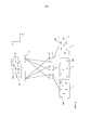
Предлагаемый лазерный прибор может быть реализован в системах формирования трехмерного изображения или системах трехмерного измерения. Такая система содержит камеру, которая формируют изображение сцены, на которую проецируют структурированную картину освещения, интерфейс синхронизации между камерой и лазерным прибором и вычислительный блок, извлекающий трехмерную информацию из изображения камеры. Интерфейс синхронизации обеспечивает то, что изображения сцены получаются только во время освещения с использованием структурированной картины освещения. Такая система также включает в себя по меньшей мере один блок питания для лазерного прибора. Также могут быть использованы несколько блоков питания, один для каждой матрицы или кристалла. Для последовательного функционирования по меньшей мере часть схем может быть использована совместно.The proposed laser device can be implemented in three-dimensional imaging systems or three-dimensional measurement systems. Such a system comprises a camera that forms an image of a scene onto which a structured illumination picture is projected, a synchronization interface between the camera and the laser device, and a computing unit that extracts three-dimensional information from the camera image. The synchronization interface ensures that scene images are only obtained during lighting using a structured lighting pattern. Such a system also includes at least one power supply for the laser device. Multiple power supplies can also be used, one for each matrix or chip. For consistent operation, at least a portion of the circuits may be used together.
Эти и другие аспекты настоящего изобретения станут очевидны из вариантов осуществления, описанных ниже, и будут объяснены со ссылкой ни них.These and other aspects of the present invention will become apparent from the embodiments described below, and will be explained with reference to them.
КРАТКОЕ ОПИСАНИЕ ЧЕРТЕЖЕЙBRIEF DESCRIPTION OF THE DRAWINGS
Предлагаемый лазерный прибор описан далее посредством примеров, связанных с сопутствующими чертежами для дополнительных подробностей. Эти фигуры показывают:The proposed laser device is described below by way of examples associated with the accompanying drawings for further details. These figures show:
Фиг. 1 представляет собой пример проекции одной из матриц VCSEL предлагаемого прибора на плоскость изображения,FIG. 1 is an example of a projection of one of the VCSEL matrices of the proposed device on the image plane,
Фиг. 2 представляет собой пример рандомизированного распределения VCSEL в матрице VCSEL предлагаемого лазерного прибора;FIG. 2 is an example of a randomized distribution of VCSEL in a VCSEL matrix of a laser device of the invention;
Фиг. 3 – схематичный вид, иллюстрирующий наложение разных матриц VCSEL предлагаемого лазерного прибора в пространстве изображений; иFIG. 3 is a schematic view illustrating the superposition of different VCSEL matrices of the proposed laser device in the image space; and
Фиг. 4 представляет собой схематичный вид, показывающий систему формирования трехмерного изображения, включающую в себя предлагаемый лазерный прибор.FIG. 4 is a schematic view showing a three-dimensional imaging system including the proposed laser device.
ПОДРОБНОЕ ОПИСАНИЕ ВАРИАНТОВ ОСУЩЕСТВЛЕНИЯDETAILED DESCRIPTION OF EMBODIMENTS
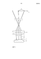
Предлагаемый лазерный прибор содержит несколько полупроводниковых матриц с соответствующими оптическими устройствами для формирования изображения излучающих областей полупроводниковых лазеров в пространстве изображений. Фиг. 1 показывает пример для базовой компоновки одного модуля предлагаемого лазерного прибора. Каждый модуль содержит одну из матриц VCSEL, используемых в этом примере. Матрица VCSEL предусмотрена в корпусе, обеспечивающем электрические контакты и теплоотвод. Фиг. 1 показывает соответствующий кристалл 1 VCSEL, несущий матрицу VCSEL с несколькими VCSEL 2. Кристалл 1 VCSEL установлен на радиатор 3 для теплоотвода. Формирующий изображение объектив 4 расположен перед кристаллом 1 VCSEL для формирования изображения излучающих областей отдельных VCSEL 2 матрицы на плоскости изображения в требуемом пространстве изображений. Пространство изображений является областью с глубиной, также называемой областью захвата в случае системы формирования трехмерного изображения, в которой формируют изображение матрицы VCSEL посредством объектива 4. Условия формирования изображения для формирования изображения, например, VCSEL 2, имеющего диаметр активной области 4 мкм, в пространстве изображений являются очень похожими на условия для формирования изображения сцены в пространстве изображений на кристалле камеры с равным размером пикселей, поскольку это соответствует только обратному пути света. Следовательно, может быть использован недорогой и похожий объектив 4 в предлагаемом лазерном приборе. С помощью этого формирующего изображение объектива 4 лазерные лучи 5, излучаемые VCSEL 2, фокусируют в пятна лучей 6 в пространстве изображений. Форма этих пятен лучей на плоскости изображения 7 соответствует форме излучающих областей VCSEL 2 кристалла 1 VCSEL.The proposed laser device contains several semiconductor arrays with corresponding optical devices for imaging the radiating regions of semiconductor lasers in the image space. FIG. 1 shows an example for the basic layout of one module of the proposed laser device. Each module contains one of the VCSEL matrices used in this example. The VCSEL matrix is provided in a housing that provides electrical contacts and a heat sink. FIG. 1 shows a corresponding
Для формирования изображения от нескольких кристаллов 1 VCSEL этот модуль должен быть повторен. Если несколько модулей помещены рядом друг с другом на одной плоскости установки, то перекрытие изображений матриц VCSEL в дальней зоне, например, в пространстве изображений, уже является хорошим без дополнительной юстировки. При необходимости формирующие изображение объективы 4 каждого из модулей могут быть незначительно юстированы так, чтобы пятна лучей VCSEL 2 разных кристаллов 1 VCSEL не перекрывались в пространстве изображений. Для улучшения юстировки объективов могут быть обеспечены юстировочные метки в конкретных специальных излучающих областях, на каждой матрице, которые должны быть наложены в плоскости изображений для оптимальной юстировки. Если юстировка невозможна, то электронная калибровка изображения камеры, полученного из тестовой сцены, может учитывать незначительные неточности в изготовлении, чтобы узнать точное распределение пятен лучей в пространстве изображений, которое необходимо для трехмерного распознавания сцен. При необходимости может быть обеспечена механическая юстировка, например, положения формирующего изображение объектива 4 относительно кристалла 1 VCSEL. Это могло бы, например, обеспечить возможность регулировки распределения интервалов пятен лучей в пространстве изображений между вертикальным и горизонтальным направлением.To form an image from several crystals of 1 VCSEL, this module must be repeated. If several modules are placed next to each other on the same installation plane, then overlapping images of VCSEL matrices in the far zone, for example, in the image space, is already good without additional adjustment. If necessary, the
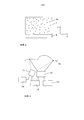
Кристаллы 1 VCSEL предлагаемого лазерного прибора изготавливают так, чтобы положение отдельных VCSEL 2 на кристалле, в частности, излучающих областей VCSEL 2, отклонялось от регулярной структуры рандомизированным образом или полностью распределялось рандомизированным образом. Фиг. 2 показывает схематичный вид примера такого распределения излучающих областей 2а VCSEL 2 на кристалле 1. Контактная площадка 8 для электрического контакта VCSEL 2 также показана в этой компоновке матрицы. Как можно увидеть на фиг. 2, излучающие области 2а VCSEL 2 расположены в рандомизированном распределении без какой-либо периодичности или регулярности.The
Далее дан численный пример компоновки кристалла для кристалла 1 VCSEL предлагаемого лазерного прибора. Активный диаметр излучающих областей 2а единичного кристалла VCSEL 2 может быть около 4 мкм. Этот диаметр является достаточным для мощности 3 мВт при работе в импульсном режиме, например, 100 мкс. Соответствующий шаг в регулярной структуре таких излучающих областей или VCSEL на кристалле может быть 42 мкм при оставлении места для рандомизации +/- 4 мкм. Этот шаг вычисляют по формуле: шаг =30 мкм+3*d, где d представляет собой активный диаметр. В данном примере три матрицы VCSEL или кристалла 1 VCSEL использованы в лазерном приборе. Каждый кристалл содержит 100 VCSEL в горизонтальном (x-) направлении и 40 VCSELs в вертикальном (y-) направлении, что приводит к размеру кристалла 4,2 мм x 1,68 мм. Общая площадь кристалла (все три кристалла) составляет 21,2 мм2. Наложение соответствующих оптических устройств формирования изображения выполняют, главным образом, в горизонтальном направлении, что означает, что среднее расстояние между пятнами лучей по горизонтали в три раза меньшей, чем по вертикали в плоскости формирования изображения.The following is a numerical example of the layout of the crystal for
Благодаря использованию соответствующих оптических устройств формирования изображения дополнительно возможно сжатие в вертикальном направлении, если требуется. Это обеспечивает возможность более равномерных интервалов между пятнами лучей в горизонтальном и вертикальном направлении в изложенном выше случае, в котором наложение выполняют, главным образом, в горизонтальном направлении. При необходимости, форма излучающих областей VCSEL может быть предусмотрена для такого сжатия, т.е. вертикальный размер (y-размер) активных областей VCSEL может быть выбран большим, чем горизонтальный размер (x-размер), таким образом, чтобы упомянутое выше сжатие привело к обеспечению приблизительно равных горизонтального и вертикального размеров.Thanks to the use of appropriate optical imaging devices, vertical compression is additionally possible if required. This allows more uniform intervals between the spots of rays in the horizontal and vertical direction in the above case, in which the overlay is performed mainly in the horizontal direction. If necessary, the shape of the VCSEL emitting regions can be provided for such compression, i.e. the vertical size (y-size) of the VCSEL active regions can be selected larger than the horizontal size (x-size) so that the compression mentioned above results in approximately equal horizontal and vertical sizes.
Оптическое устройство формирования изображения может быть также выполнено таким, чтобы изображения разных матриц незначительно смещались в вертикальном направлении, чтобы иметь одинаковые интервалы между пятнами лучей в обоих направлениях, вместо выравнивания вдоль горизонтальных линий с темными областями между ними.The optical imaging device can also be designed so that the images of different matrices are slightly offset in the vertical direction so as to have the same intervals between the spots of rays in both directions, instead of aligning along horizontal lines with dark areas between them.
VCSEL разных матриц могут быть выбраны имеющими разные формы активной области. Фиг. 3 показывает три разные компоновки матрицы, имеющие прямоугольную форму в вертикальном направлении, круглую форму и прямоугольную форму в горизонтальном направлении. Изображения трех кристаллов 1 VCSEL формируется с помощью соответствующих формирующих изображение объективов 4 на плоскости изображения 7, как схематично показано на фигуре. Результирующая картина 9 освещения показана на верхнем участке фиг. 3. Как можно увидеть из этой картины 9 освещения, изображения пятен лучей 6, исходящих из каждого кристалла 1 VCSEL, сформированы в интервалах между пятнами лучей 6 остальных кристаллов VCSEL, соответственно. Это приводит к картине 9 освещения, на которой разные формы VCSEL разных кристаллов 1 VCSEL смешаны в плоскости изображения 7.VCSELs of different matrices can be selected having different shapes of the active region. FIG. 3 shows three different matrix arrangements having a rectangular shape in the vertical direction, a circular shape and a rectangular shape in the horizontal direction. Images of three
Использование упомянутых выше трех разных форм VCSEL может уменьшить необходимое количество пятен лучей для систем формирования трехмерного изображения по меньшей мере в два раза. Предполагая, что равный участок каждой формы является наиболее эффективными для предотвращения неопределенностей, количества 2000 VCSEL каждой формы было бы достаточно для замены 12000 пятен лучей согласно упомянутым выше требованиям стандарта безопасности EU-NCAP. При разделении этого числа VCSEL на три матрицы каждая матрица может иметь размеры, например, 2,75 мм x 2,2 мм. Этот размер вычислен с использованием предположения, что круглая область = прямоугольной области (4×8 мкм2)=32 мкм2, т.е., диаметр окружности =6,4 мкм, и с шагом для матрицы окружностей минимум 50 мкм, предпочтительно до 55 мкм, чтобы иметь равные условия с матрицами прямоугольников с максимальным размером 8 мкм.Using the above three different VCSEL shapes can reduce the required number of ray spots for 3D imaging systems by at least half. Assuming that an equal area of each shape is most effective in preventing uncertainties, a quantity of 2000 VCSELs of each shape would be sufficient to replace 12,000 beam spots according to the above mentioned EU-NCAP safety standard requirements. When dividing this VCSEL number into three matrices, each matrix can have dimensions, for example, 2.75 mm x 2.2 mm. This size is calculated using the assumption that the circular region = rectangular region (4 × 8 μm 2 ) = 32 μm 2 , i.e., the diameter of the circle = 6.4 μm, and with a pitch for the matrix of circles of at least 50 μm, preferably up to 55 microns to have equal conditions with matrices of rectangles with a maximum size of 8 microns.
В примере из фиг. 3 разные формы VCSEL обеспечены на разных матрицах. Также возможно смешение разных форм на единственных матрицах. В таком варианте осуществления области разных форм должны быть выбраны так, чтобы VCSEL имели похожий пороговый ток.In the example of FIG. 3 different VCSEL forms are provided on different matrices. It is also possible to mix different forms on single matrices. In such an embodiment, regions of different shapes should be selected so that the VCSELs have a similar threshold current.
Фиг. 4 показывает схематичный вид примера системы трехмерного измерения, включающей в себя предлагаемый лазерный прибор 10. Эта система также включает в себя камеру 11, получающую изображения структурированной картины освещения, спроецированной на сцену 15. Камера 11 соединена через блок 12 синхронизации с лазерным прибором 10 для ее синхронизации с импульсным освещением сцены. Блоки питания лазерного прибора 10 могут быть соединены с блоком 13 управления для последовательного функционирования разных кристаллов VCSEL прибора 10. Вычислительный блок 14 может быть предусмотрен для извлечения требуемой трехмерной информации из изображения или изображений, захваченных камерой 11. Такая система может быть использована в применениях, уже описанных во вводной части описания, в частности, в применениях в области автомобилестроения для захвата сцены перед автомобилем.FIG. 4 shows a schematic view of an example of a three-dimensional measurement system including the proposed
В то время как данное изобретение показано и описано в подробностях на чертежах и в предшествующем описании, такие иллюстрация и описание, как предполагается, являются иллюстративными или примерными, а не ограничивающими; данное изобретение не ограничено раскрытыми вариантами осуществления. Другие вариации раскрытых вариантов осуществления могут быть поняты и осуществлены специалистами в данной области техники при реализации заявленного изобретения из изучения чертежей, раскрытия, и приложенной формулы изобретения. Матрицы предлагаемого лазерного прибора могут быть расположены в любой конфигурации, например, в линию или треугольником. Также, только две матрицы или более чем три матрицы могут быть предусмотрены для достижения необходимого наложения. Кроме того, число полупроводниковых лазеров каждой матрицы может отличаться от приведенного выше примера в зависимости от требуемого разрешения системы. Вместо VCSEL могут быть использованы другие типы полупроводниковых лазеров, например, торцевые излучатели. В формуле изобретения, слово «содержащий» не исключает других элементов или этапов, а неопределенный артикль не исключает множества. Тот факт, что некоторые меры перечислены во взаимно отличающихся зависимых пунктах формулы изобретения, не указывает на то, что комбинация этих мер не может быть использована для получения выгоды. Признаки всех пунктов формулы изобретения упомянутого прибора могут быть скомбинированы свободным образом. Любые ссылочные позиции в формуле изобретения не должны быть истолкованы как ограничения объема данного изобретения.While the invention has been shown and described in detail in the drawings and in the foregoing description, such illustration and description are intended to be illustrative or exemplary and not limiting; the invention is not limited to the disclosed embodiments. Other variations of the disclosed embodiments may be understood and practiced by those skilled in the art when implementing the claimed invention from a study of the drawings, disclosure, and appended claims. The matrix of the proposed laser device can be located in any configuration, for example, in a line or a triangle. Also, only two matrices or more than three matrices can be provided to achieve the necessary overlap. In addition, the number of semiconductor lasers of each matrix may differ from the above example depending on the required resolution of the system. Instead of VCSEL, other types of semiconductor lasers, such as end emitters, can be used. In the claims, the word “comprising” does not exclude other elements or steps, and the indefinite article does not exclude a plurality. The fact that some measures are listed in mutually different dependent dependent claims does not indicate that a combination of these measures cannot be used to obtain benefits. The features of all claims of the aforementioned device can be combined in a free way. Any reference position in the claims should not be construed as limiting the scope of this invention.
ПЕРЕЧЕНЬ ССЫЛОЧНЫХ ПОЗИЦИЙLIST OF REFERENCE POSITIONS
1 – кристалл VCSEL1 - VCSEL crystal
2 - VCSEL2 - VCSEL
2а - излучающая область VCSEL2a - radiating region VCSEL
3 – радиатор3 - radiator
4 – формирующий изображение объектив4 - imaging lens
5 – лазерный луч5 - laser beam
6 – лазерное пятно6 - laser spot
7 - плоскость изображения7 - image plane
8 – контактная площадка8 - contact area
9 - картина освещения9 - lighting pattern
10 – лазерный прибор10 - laser device
11 - камера11 - camera
12 – блок синхронизации12 - synchronization unit
13 - блок управления13 - control unit
14 - вычислительный блок14 - computing unit
15 - сцена15 - scene
Claims (23)
Applications Claiming Priority (3)
| Application Number | Priority Date | Filing Date | Title |
|---|---|---|---|
| US201261731037P | 2012-11-29 | 2012-11-29 | |
| US61/731,037 | 2012-11-29 | ||
| PCT/IB2013/060325 WO2014083485A1 (en) | 2012-11-29 | 2013-11-22 | Laser device for projecting a structured light pattern onto a scene |
Publications (2)
| Publication Number | Publication Date |
|---|---|
| RU2015125550A RU2015125550A (en) | 2017-01-10 |
| RU2655475C2 true RU2655475C2 (en) | 2018-05-28 |
Family
ID=50030351
Family Applications (1)
| Application Number | Title | Priority Date | Filing Date |
|---|---|---|---|
| RU2015125550A RU2655475C2 (en) | 2012-11-29 | 2013-11-22 | Laser device for projecting structured light pattern onto scene |
Country Status (7)
| Country | Link |
|---|---|
| US (1) | US10386178B2 (en) |
| EP (1) | EP2926422B1 (en) |
| JP (1) | JP6270863B2 (en) |
| CN (1) | CN104798271B (en) |
| BR (1) | BR112015012073A2 (en) |
| RU (1) | RU2655475C2 (en) |
| WO (1) | WO2014083485A1 (en) |
Cited By (1)
| Publication number | Priority date | Publication date | Assignee | Title |
|---|---|---|---|---|
| RU2718125C1 (en) * | 2019-07-11 | 2020-03-30 | Федеральное государственное бюджетное образовательное учреждение высшего образования "Московский государственный университет геодезии и картографии" (МИИГАиК) | Device for increasing projection range of structured illumination for 3d scanning |
Families Citing this family (93)
| Publication number | Priority date | Publication date | Assignee | Title |
|---|---|---|---|---|
| US8908995B2 (en) | 2009-01-12 | 2014-12-09 | Intermec Ip Corp. | Semi-automatic dimensioning with imager on a portable device |
| US9870068B2 (en) | 2010-09-19 | 2018-01-16 | Facebook, Inc. | Depth mapping with a head mounted display using stereo cameras and structured light |
| US20160025993A1 (en) * | 2014-07-28 | 2016-01-28 | Apple Inc. | Overlapping pattern projector |
| US9779546B2 (en) | 2012-05-04 | 2017-10-03 | Intermec Ip Corp. | Volume dimensioning systems and methods |
| US10007858B2 (en) | 2012-05-15 | 2018-06-26 | Honeywell International Inc. | Terminals and methods for dimensioning objects |
| US10321127B2 (en) | 2012-08-20 | 2019-06-11 | Intermec Ip Corp. | Volume dimensioning system calibration systems and methods |
| US9939259B2 (en) | 2012-10-04 | 2018-04-10 | Hand Held Products, Inc. | Measuring object dimensions using mobile computer |
| US20140104413A1 (en) | 2012-10-16 | 2014-04-17 | Hand Held Products, Inc. | Integrated dimensioning and weighing system |
| US20140307055A1 (en) * | 2013-04-15 | 2014-10-16 | Microsoft Corporation | Intensity-modulated light pattern for active stereo |
| US10228452B2 (en) | 2013-06-07 | 2019-03-12 | Hand Held Products, Inc. | Method of error correction for 3D imaging device |
| CN105324631B (en) | 2013-06-19 | 2018-11-16 | 苹果公司 | integrated structured light projector |
| CA2924622C (en) | 2013-10-23 | 2020-03-10 | Oculus Vr, Llc. | Three dimensional depth mapping using dynamic structured light |
| WO2015134794A2 (en) | 2014-03-05 | 2015-09-11 | Smart Picture Technologies, Inc. | Method and system for 3d capture based on structure from motion with simplified pose detection |
| US10760971B2 (en) * | 2014-03-13 | 2020-09-01 | National University Of Singapore | Optical interference device |
| US20150369593A1 (en) * | 2014-06-19 | 2015-12-24 | Kari MYLLYKOSKI | Orthographic image capture system |
| US9823059B2 (en) | 2014-08-06 | 2017-11-21 | Hand Held Products, Inc. | Dimensioning system with guided alignment |
| EP3074721B1 (en) * | 2014-08-08 | 2021-05-19 | CEMB S.p.A. | Vehicle equipment with scanning system for contactless measurement |
| US20160072258A1 (en) * | 2014-09-10 | 2016-03-10 | Princeton Optronics Inc. | High Resolution Structured Light Source |
| US10775165B2 (en) | 2014-10-10 | 2020-09-15 | Hand Held Products, Inc. | Methods for improving the accuracy of dimensioning-system measurements |
| US10810715B2 (en) | 2014-10-10 | 2020-10-20 | Hand Held Products, Inc | System and method for picking validation |
| US9779276B2 (en) | 2014-10-10 | 2017-10-03 | Hand Held Products, Inc. | Depth sensor based auto-focus system for an indicia scanner |
| US9752864B2 (en) | 2014-10-21 | 2017-09-05 | Hand Held Products, Inc. | Handheld dimensioning system with feedback |
| US9897434B2 (en) | 2014-10-21 | 2018-02-20 | Hand Held Products, Inc. | Handheld dimensioning system with measurement-conformance feedback |
| US10060729B2 (en) | 2014-10-21 | 2018-08-28 | Hand Held Products, Inc. | Handheld dimensioner with data-quality indication |
| US10509147B2 (en) | 2015-01-29 | 2019-12-17 | ams Sensors Singapore Pte. Ltd | Apparatus for producing patterned illumination using arrays of light sources and lenses |
| US9273846B1 (en) | 2015-01-29 | 2016-03-01 | Heptagon Micro Optics Pte. Ltd. | Apparatus for producing patterned illumination including at least one array of light sources and at least one array of microlenses |
| US9553423B2 (en) * | 2015-02-27 | 2017-01-24 | Princeton Optronics Inc. | Miniature structured light illuminator |
| WO2016154218A1 (en) * | 2015-03-22 | 2016-09-29 | Oculus Vr, Llc | Depth mapping with a head mounted display using stereo cameras and structured light |
| US10001583B2 (en) * | 2015-04-06 | 2018-06-19 | Heptagon Micro Optics Pte. Ltd. | Structured light projection using a compound patterned mask |
| US9786101B2 (en) | 2015-05-19 | 2017-10-10 | Hand Held Products, Inc. | Evaluating image values |
| US10066982B2 (en) | 2015-06-16 | 2018-09-04 | Hand Held Products, Inc. | Calibrating a volume dimensioner |
| KR102311688B1 (en) | 2015-06-17 | 2021-10-12 | 엘지전자 주식회사 | Mobile terminal and method for controlling the same |
| US10083522B2 (en) | 2015-06-19 | 2018-09-25 | Smart Picture Technologies, Inc. | Image based measurement system |
| US20160377414A1 (en) * | 2015-06-23 | 2016-12-29 | Hand Held Products, Inc. | Optical pattern projector |
| US9835486B2 (en) | 2015-07-07 | 2017-12-05 | Hand Held Products, Inc. | Mobile dimensioner apparatus for use in commerce |
| EP3396313B1 (en) | 2015-07-15 | 2020-10-21 | Hand Held Products, Inc. | Mobile dimensioning method and device with dynamic accuracy compatible with nist standard |
| US20170017301A1 (en) | 2015-07-16 | 2017-01-19 | Hand Held Products, Inc. | Adjusting dimensioning results using augmented reality |
| US10094650B2 (en) | 2015-07-16 | 2018-10-09 | Hand Held Products, Inc. | Dimensioning and imaging items |
| CN105222729A (en) * | 2015-10-30 | 2016-01-06 | 上海斐讯数据通信技术有限公司 | Road surface evenness degree detection method and device |
| US10249030B2 (en) | 2015-10-30 | 2019-04-02 | Hand Held Products, Inc. | Image transformation for indicia reading |
| US10225544B2 (en) | 2015-11-19 | 2019-03-05 | Hand Held Products, Inc. | High resolution dot pattern |
| US10025314B2 (en) | 2016-01-27 | 2018-07-17 | Hand Held Products, Inc. | Vehicle positioning and object avoidance |
| WO2017135894A1 (en) | 2016-02-01 | 2017-08-10 | Heptagon Micro Optics Pte. Ltd. | Illumination modules and optoelectronic systems |
| WO2017163173A1 (en) * | 2016-03-23 | 2017-09-28 | Koninklijke Philips N.V. | Systems and methods for projecting multiple images on a common area of an outer surface of a housing |
| US10761195B2 (en) * | 2016-04-22 | 2020-09-01 | OPSYS Tech Ltd. | Multi-wavelength LIDAR system |
| KR101892013B1 (en) | 2016-05-27 | 2018-08-27 | 엘지전자 주식회사 | Mobile terminal |
| US10393877B2 (en) * | 2016-06-01 | 2019-08-27 | Velodyne Lidar, Inc. | Multiple pixel scanning LIDAR |
| US10339352B2 (en) | 2016-06-03 | 2019-07-02 | Hand Held Products, Inc. | Wearable metrological apparatus |
| US20170353712A1 (en) * | 2016-06-06 | 2017-12-07 | Raymond Kirk Price | Pulsed gated structured light systems and methods |
| US9940721B2 (en) | 2016-06-10 | 2018-04-10 | Hand Held Products, Inc. | Scene change detection in a dimensioner |
| US10163216B2 (en) | 2016-06-15 | 2018-12-25 | Hand Held Products, Inc. | Automatic mode switching in a volume dimensioner |
| US9947099B2 (en) * | 2016-07-27 | 2018-04-17 | Microsoft Technology Licensing, Llc | Reflectivity map estimate from dot based structured light systems |
| US10241244B2 (en) | 2016-07-29 | 2019-03-26 | Lumentum Operations Llc | Thin film total internal reflection diffraction grating for single polarization or dual polarization |
| US10909708B2 (en) | 2016-12-09 | 2021-02-02 | Hand Held Products, Inc. | Calibrating a dimensioner using ratios of measurable parameters of optic ally-perceptible geometric elements |
| CN110402398B (en) | 2017-03-13 | 2023-12-01 | 欧普赛斯技术有限公司 | Eye-safe scanning lidar system |
| US11047672B2 (en) | 2017-03-28 | 2021-06-29 | Hand Held Products, Inc. | System for optically dimensioning |
| US10386465B2 (en) | 2017-03-31 | 2019-08-20 | Velodyne Lidar, Inc. | Integrated LIDAR illumination power control |
| CN106972347B (en) * | 2017-05-04 | 2019-04-09 | 深圳奥比中光科技有限公司 | Laser array for 3D imaging |
| CN107039885B (en) * | 2017-05-04 | 2023-04-18 | 奥比中光科技集团股份有限公司 | Laser array applied to 3D imaging |
| CN115575928A (en) | 2017-05-08 | 2023-01-06 | 威力登激光雷达美国有限公司 | LIDAR data acquisition and control |
| CN107026392B (en) | 2017-05-15 | 2022-12-09 | 奥比中光科技集团股份有限公司 | VCSEL array light source |
| CN107424188B (en) | 2017-05-19 | 2020-06-30 | 深圳奥比中光科技有限公司 | Structured light projection module based on VCSEL array light source |
| CN106997603B (en) * | 2017-05-19 | 2020-04-17 | 深圳奥比中光科技有限公司 | Depth camera based on VCSEL array light source |
| US10733748B2 (en) | 2017-07-24 | 2020-08-04 | Hand Held Products, Inc. | Dual-pattern optical 3D dimensioning |
| CN110914702B (en) | 2017-07-28 | 2022-06-28 | 欧普赛斯技术有限公司 | VCSEL array LIDAR transmitter with small angular divergence |
| US10304254B2 (en) | 2017-08-08 | 2019-05-28 | Smart Picture Technologies, Inc. | Method for measuring and modeling spaces using markerless augmented reality |
| US10153614B1 (en) | 2017-08-31 | 2018-12-11 | Apple Inc. | Creating arbitrary patterns on a 2-D uniform grid VCSEL array |
| DE102017215850B4 (en) * | 2017-09-08 | 2019-12-24 | Robert Bosch Gmbh | Process for producing a diffractive optical element, LIDAR system with a diffractive optical element and motor vehicle with a LIDAR system |
| CN109521578B (en) | 2017-09-19 | 2021-02-26 | 奥比中光科技集团股份有限公司 | Depth camera |
| CN107678225A (en) * | 2017-09-19 | 2018-02-09 | 深圳奥比中光科技有限公司 | Structured light projection module based on high density VCSEL array light source |
| EP3710855A4 (en) | 2017-11-15 | 2021-08-04 | Opsys Tech Ltd. | Noise adaptive solid-state lidar system |
| EP3518356A1 (en) * | 2018-01-24 | 2019-07-31 | Koninklijke Philips N.V. | Laser arrangement with irregular emission pattern |
| CN108363267A (en) * | 2018-02-14 | 2018-08-03 | 深圳奥比中光科技有限公司 | The structured light projection module of regular array light source |
| CN108493767B (en) * | 2018-03-12 | 2019-09-27 | Oppo广东移动通信有限公司 | Laser generator, structured light projector, image obtain structure and electronic device |
| KR102506579B1 (en) | 2018-04-01 | 2023-03-06 | 옵시스 테크 엘티디 | Noise Adaptive Solid-State LIDAR System |
| US10584962B2 (en) | 2018-05-01 | 2020-03-10 | Hand Held Products, Inc | System and method for validating physical-item security |
| DE102018210282A1 (en) * | 2018-06-25 | 2020-01-02 | Volkswagen Aktiengesellschaft | Device and method for producing a three-dimensional object made up of at least one material layer |
| US10627709B2 (en) | 2018-06-29 | 2020-04-21 | Ricoh Company, Ltd. | Light source, projection device, measurement device, robot, electronic device, mobile object, and shaping apparatus |
| EP3598591A1 (en) * | 2018-07-17 | 2020-01-22 | Koninklijke Philips N.V. | Laser arrangement with reduced building height |
| JP7222200B2 (en) | 2018-08-27 | 2023-02-15 | 株式会社リコー | Optical devices, measuring devices, robots, electronic devices, mobile objects, and molding devices |
| US10712434B2 (en) | 2018-09-18 | 2020-07-14 | Velodyne Lidar, Inc. | Multi-channel LIDAR illumination driver |
| US20210408768A1 (en) * | 2018-09-25 | 2021-12-30 | Shenzhen Raysees Technology Co., Ltd. | Vertical Cavity Surface Emitting Laser (VCSEL) Array and Manufacturing Method |
| US11633083B2 (en) | 2018-12-20 | 2023-04-25 | Acclarent, Inc. | 3D scanning of nasal tract with deflectable endoscope |
| US11137246B2 (en) * | 2019-01-31 | 2021-10-05 | Himax Technologies Limited | Optical device |
| JP7251240B2 (en) * | 2019-03-20 | 2023-04-04 | 株式会社リコー | Optical devices, detection devices and electronics |
| CN109904718B (en) * | 2019-03-25 | 2020-09-04 | Oppo广东移动通信有限公司 | Control system and control method of time-of-flight assembly and terminal |
| US11138757B2 (en) | 2019-05-10 | 2021-10-05 | Smart Picture Technologies, Inc. | Methods and systems for measuring and modeling spaces using markerless photo-based augmented reality process |
| DE102019112340A1 (en) * | 2019-05-10 | 2020-11-12 | Bircher Reglomat Ag | TOF sensor system with a lighting device with an array of individual light sources |
| US11846728B2 (en) | 2019-05-30 | 2023-12-19 | OPSYS Tech Ltd. | Eye-safe long-range LIDAR system using actuator |
| CN110412544A (en) * | 2019-08-23 | 2019-11-05 | 上海禾赛光电科技有限公司 | Laser transmitting system and laser radar including the laser transmitting system |
| US20220290976A1 (en) * | 2019-09-04 | 2022-09-15 | ams Sensors Singapore Pte. Ltd | Designing and constructing dot projectors for three-dimensional sensor modules |
| US11450083B2 (en) * | 2019-09-27 | 2022-09-20 | Honeywell International Inc. | Dual-pattern optical 3D dimensioning |
| US11639846B2 (en) | 2019-09-27 | 2023-05-02 | Honeywell International Inc. | Dual-pattern optical 3D dimensioning |
Citations (5)
| Publication number | Priority date | Publication date | Assignee | Title |
|---|---|---|---|---|
| US20050286767A1 (en) * | 2004-06-23 | 2005-12-29 | Hager Gregory D | System and method for 3D object recognition using range and intensity |
| US20070019181A1 (en) * | 2003-04-17 | 2007-01-25 | Sinclair Kenneth H | Object detection system |
| US20080232679A1 (en) * | 2005-08-17 | 2008-09-25 | Hahn Daniel V | Apparatus and Method for 3-Dimensional Scanning of an Object |
| US20110025827A1 (en) * | 2009-07-30 | 2011-02-03 | Primesense Ltd. | Depth Mapping Based on Pattern Matching and Stereoscopic Information |
| US20120293625A1 (en) * | 2011-05-18 | 2012-11-22 | Sick Ag | 3d-camera and method for the three-dimensional monitoring of a monitoring area |
Family Cites Families (15)
| Publication number | Priority date | Publication date | Assignee | Title |
|---|---|---|---|---|
| US6975659B2 (en) * | 2001-09-10 | 2005-12-13 | Fuji Photo Film Co., Ltd. | Laser diode array, laser device, wave-coupling laser source, and exposure device |
| US7440590B1 (en) * | 2002-05-21 | 2008-10-21 | University Of Kentucky Research Foundation | System and technique for retrieving depth information about a surface by projecting a composite image of modulated light patterns |
| CN101816185B (en) | 2007-10-05 | 2012-11-14 | 皇家飞利浦电子股份有限公司 | Image projection method |
| US8159682B2 (en) * | 2007-11-12 | 2012-04-17 | Intellectual Ventures Holding 67 Llc | Lens system |
| WO2009153699A1 (en) * | 2008-06-18 | 2009-12-23 | Philips Intellectual Property & Standards Gmbh | Driver assistance system |
| US8531650B2 (en) | 2008-07-08 | 2013-09-10 | Chiaro Technologies LLC | Multiple channel locating |
| DE202008017962U1 (en) | 2008-09-23 | 2011-02-10 | Sick Ag | Illumination unit for generating a self-similar pattern |
| US8215776B2 (en) | 2009-01-07 | 2012-07-10 | Eastman Kodak Company | Line illumination apparatus using laser arrays |
| JP2010251113A (en) * | 2009-04-15 | 2010-11-04 | Sony Corp | Method of manufacturing solid electrolyte battery, and solid electrolyte battery |
| CN102742100B (en) | 2009-08-20 | 2015-06-03 | 皇家飞利浦电子股份有限公司 | Laser device with configurable intensity distribution |
| US8320621B2 (en) | 2009-12-21 | 2012-11-27 | Microsoft Corporation | Depth projector system with integrated VCSEL array |
| US8755036B2 (en) * | 2010-03-11 | 2014-06-17 | Optical Physics Company | Active imaging system and method |
| JP2012177671A (en) * | 2011-02-27 | 2012-09-13 | Plex International Design Co Ltd | Fine aperiodic pattern projection device and method and three-dimensional measuring device using the same |
| CN102760234B (en) | 2011-04-14 | 2014-08-20 | 财团法人工业技术研究院 | Depth image acquisition device, system and method |
| US9797708B2 (en) | 2012-05-14 | 2017-10-24 | Koninklijke Philips N.V. | Apparatus and method for profiling a depth of a surface of a target object |
-
2013
- 2013-11-22 RU RU2015125550A patent/RU2655475C2/en not_active IP Right Cessation
- 2013-11-22 EP EP13826602.8A patent/EP2926422B1/en active Active
- 2013-11-22 BR BR112015012073A patent/BR112015012073A2/en not_active Application Discontinuation
- 2013-11-22 JP JP2015544580A patent/JP6270863B2/en not_active Expired - Fee Related
- 2013-11-22 CN CN201380062417.4A patent/CN104798271B/en active Active
- 2013-11-22 WO PCT/IB2013/060325 patent/WO2014083485A1/en active Application Filing
- 2013-11-22 US US14/647,836 patent/US10386178B2/en active Active
Patent Citations (5)
| Publication number | Priority date | Publication date | Assignee | Title |
|---|---|---|---|---|
| US20070019181A1 (en) * | 2003-04-17 | 2007-01-25 | Sinclair Kenneth H | Object detection system |
| US20050286767A1 (en) * | 2004-06-23 | 2005-12-29 | Hager Gregory D | System and method for 3D object recognition using range and intensity |
| US20080232679A1 (en) * | 2005-08-17 | 2008-09-25 | Hahn Daniel V | Apparatus and Method for 3-Dimensional Scanning of an Object |
| US20110025827A1 (en) * | 2009-07-30 | 2011-02-03 | Primesense Ltd. | Depth Mapping Based on Pattern Matching and Stereoscopic Information |
| US20120293625A1 (en) * | 2011-05-18 | 2012-11-22 | Sick Ag | 3d-camera and method for the three-dimensional monitoring of a monitoring area |
Cited By (1)
| Publication number | Priority date | Publication date | Assignee | Title |
|---|---|---|---|---|
| RU2718125C1 (en) * | 2019-07-11 | 2020-03-30 | Федеральное государственное бюджетное образовательное учреждение высшего образования "Московский государственный университет геодезии и картографии" (МИИГАиК) | Device for increasing projection range of structured illumination for 3d scanning |
Also Published As
| Publication number | Publication date |
|---|---|
| WO2014083485A1 (en) | 2014-06-05 |
| EP2926422A1 (en) | 2015-10-07 |
| BR112015012073A2 (en) | 2017-07-11 |
| JP2016507886A (en) | 2016-03-10 |
| US20150316368A1 (en) | 2015-11-05 |
| US10386178B2 (en) | 2019-08-20 |
| CN104798271A (en) | 2015-07-22 |
| JP6270863B2 (en) | 2018-01-31 |
| EP2926422B1 (en) | 2017-11-22 |
| RU2015125550A (en) | 2017-01-10 |
| CN104798271B (en) | 2018-08-28 |
Similar Documents
| Publication | Publication Date | Title |
|---|---|---|
| RU2655475C2 (en) | Laser device for projecting structured light pattern onto scene | |
| US11320666B2 (en) | Integrated structured-light projector | |
| CN107026392B (en) | VCSEL array light source | |
| KR102231081B1 (en) | Projectors of structured light | |
| US9825425B2 (en) | Integrated structured-light projector comprising light-emitting elements on a substrate | |
| CN107533239A (en) | Optical scanning control device | |
| CN108388071B (en) | Depth camera and projection module thereof | |
| US20140313524A1 (en) | Method and Device for Three-Dimensional Confocal Measurement | |
| JP2013190394A (en) | Pattern illumination apparatus and distance measuring apparatus | |
| US20220123530A1 (en) | Vertical cavity surface emitting laser (vcsel) based pattern projector | |
| US20150369588A1 (en) | Optical measurement apparatus and method of controlling the same | |
| TWI444609B (en) | Surface-scanning unit and optical detecting appratus having the same | |
| JP7374165B2 (en) | Dot pattern projector used in 3D distance measurement system |
Legal Events
| Date | Code | Title | Description |
|---|---|---|---|
| MM4A | The patent is invalid due to non-payment of fees |
Effective date: 20201123 |