RU2212704C2 - Shared cache structure for timing and non-timing commands - Google Patents
Shared cache structure for timing and non-timing commandsInfo
- Publication number
- RU2212704C2 RU2212704C2 RU2000127102/09A RU2000127102A RU2212704C2 RU 2212704 C2 RU2212704 C2 RU 2212704C2 RU 2000127102/09 A RU2000127102/09 A RU 2000127102/09A RU 2000127102 A RU2000127102 A RU 2000127102A RU 2212704 C2 RU2212704 C2 RU 2212704C2
- Authority
- RU
- Russia
- Prior art keywords
- cache
- data
- bit
- temporary
- memory
- Prior art date
Links
Images
Classifications
-
- G—PHYSICS
- G06—COMPUTING; CALCULATING OR COUNTING
- G06F—ELECTRIC DIGITAL DATA PROCESSING
- G06F12/00—Accessing, addressing or allocating within memory systems or architectures
- G06F12/02—Addressing or allocation; Relocation
- G06F12/08—Addressing or allocation; Relocation in hierarchically structured memory systems, e.g. virtual memory systems
- G06F12/0802—Addressing of a memory level in which the access to the desired data or data block requires associative addressing means, e.g. caches
- G06F12/0875—Addressing of a memory level in which the access to the desired data or data block requires associative addressing means, e.g. caches with dedicated cache, e.g. instruction or stack
-
- G—PHYSICS
- G06—COMPUTING; CALCULATING OR COUNTING
- G06F—ELECTRIC DIGITAL DATA PROCESSING
- G06F12/00—Accessing, addressing or allocating within memory systems or architectures
- G06F12/02—Addressing or allocation; Relocation
- G06F12/08—Addressing or allocation; Relocation in hierarchically structured memory systems, e.g. virtual memory systems
- G06F12/0802—Addressing of a memory level in which the access to the desired data or data block requires associative addressing means, e.g. caches
- G06F12/0864—Addressing of a memory level in which the access to the desired data or data block requires associative addressing means, e.g. caches using pseudo-associative means, e.g. set-associative or hashing
-
- G—PHYSICS
- G06—COMPUTING; CALCULATING OR COUNTING
- G06F—ELECTRIC DIGITAL DATA PROCESSING
- G06F12/00—Accessing, addressing or allocating within memory systems or architectures
- G06F12/02—Addressing or allocation; Relocation
- G06F12/08—Addressing or allocation; Relocation in hierarchically structured memory systems, e.g. virtual memory systems
- G06F12/12—Replacement control
- G06F12/121—Replacement control using replacement algorithms
- G06F12/126—Replacement control using replacement algorithms with special data handling, e.g. priority of data or instructions, handling errors or pinning
-
- G—PHYSICS
- G06—COMPUTING; CALCULATING OR COUNTING
- G06F—ELECTRIC DIGITAL DATA PROCESSING
- G06F12/00—Accessing, addressing or allocating within memory systems or architectures
- G06F12/02—Addressing or allocation; Relocation
- G06F12/08—Addressing or allocation; Relocation in hierarchically structured memory systems, e.g. virtual memory systems
- G06F12/0802—Addressing of a memory level in which the access to the desired data or data block requires associative addressing means, e.g. caches
- G06F12/0862—Addressing of a memory level in which the access to the desired data or data block requires associative addressing means, e.g. caches with prefetch
Abstract
Description
Предпосылки изобретения
1. Область техники, к которой относится изобретение
Данное изобретение относится вообще к области процессоров и, в частности, к технике обеспечения структуры совместно используемого кэша для временных и невременных команд.BACKGROUND OF THE INVENTION
1. The technical field to which the invention relates.
This invention relates generally to the field of processors and, in particular, to a technique for providing a shared cache structure for temporary and temporary teams.
2. Уровень техники
Использование кэш-памяти с процессором способствует уменьшению времени доступа к памяти. Основная идея организации кэша состоит в том, что при хранении наиболее часто запрашиваемых команд и данных в быстрой кэш-памяти среднее время доступа к памяти почти равно времени выборки из кэша. Для достижения максимально возможной скорости работы типовые процессоры используют кэш-иерархию, т. е. различные уровни кэш-памяти. Различные уровни кэша соответствуют различным расстояниям от процессорного ядра. Чем ближе кэш к процессору, тем быстрее доступ к данным. Тем не менее, чем быстрее доступ к данным, тем это дороже для хранения данных. В результате, чем ближе уровень кэша, тем быстрее и меньше кэш.2. The level of technology
Using a cache with a processor reduces memory access time. The main idea of organizing a cache is that when storing the most frequently requested commands and data in fast cache, the average access time to the memory is almost equal to the time of fetching from the cache. To achieve the highest possible speed, typical processors use a cache hierarchy, i.e., different levels of cache memory. Different cache levels correspond to different distances from the processor core. The closer the cache to the processor, the faster access to data. However, the faster access to data, the more expensive it is to store data. As a result, the closer the cache level, the faster and smaller the cache.
Рабочая характеристика кэш-памяти часто измеряется в показателях ее результативности. Когда процессор обращается к памяти и находит слово в кэше, говорят, что производится результативное обращение. Если слово не найдено в кэше, значит оно находится в основной памяти, и это считается промахом. Если появляется промах, тогда делается назначение в записи, индексированной при доступе. Доступ может производиться для загрузки данных в процессор или хранения данных из процессора в памяти. Кэшированная информация сохраняется кэш-памятью до тех пор, пока не отпадает в ней необходимость, пока она не становится недействительной или не заменяется другими данными, в этих случаях запись кэша переназначается. The performance of a cache is often measured in terms of performance. When the processor accesses the memory and finds the word in the cache, they say that the result is accessed effectively. If the word is not found in the cache, then it is in the main memory, and this is considered a miss. If a slip occurs, then an assignment is made to the entry indexed on access. Access can be made to load data into the processor or store data from the processor in memory. Cached information is stored in the cache until it is no longer necessary, until it becomes invalid or replaced by other data, in these cases, the cache entry is reassigned.
В процессорах, использующих кэш-иерархию, например процессорах Pentium Pro, которые имеют кэш L1 и L2, более быстрый и более малый кэш L1 располагается ближе к процессору, чем кэш L2. Когда процессор запрашивает помещаемые в кэш данные, например команду загрузки, запрос сначала посылается в кэш L1. Если запрашиваемые данные находятся в кэше L1, они доставляются процессору. В противном случае имеет место неудачное (безрезультативное) обращение в кэш L1, и запрос передается к кэшу L2. Аналогично, если имеет место результативное обращение в кэш L2, данные передаются в кэш L1 и ядро процессора. Если имеет место неудачное обращение в кэш L2, запрос передается к основной памяти. Основная память реагирует на неудачное обращение в кэш L2 предоставлением запрошенных данных в кэш L2, кэш L1 и ядро процессора. For processors using a cache hierarchy, such as Pentium Pro processors that have L1 and L2 cache, the faster and smaller L1 cache is closer to the processor than the L2 cache. When the processor requests cache data, such as a load command, the request is first sent to L1 cache. If the requested data is in the L1 cache, it is delivered to the processor. Otherwise, an unsuccessful (inconclusive) access to the L1 cache takes place, and the request is transmitted to the L2 cache. Similarly, if there is a successful hit in the L2 cache, data is transferred to the L1 cache and the processor core. If there is an unsuccessful appeal to the L2 cache, the request is transferred to the main memory. The main memory responds to unsuccessful access to the L2 cache by providing the requested data to the L2 cache, L1 cache, and the processor core.
Тип данных, которые обычно хранятся в кэше, включает активные части программ и данных. Когда кэш полон, необходимо заменить существующие строки запомненных данных в кэш-памяти, чтобы освободить пространство для вновь запрашиваемых строк данных. Одна такая техника замещения включает использование алгоритма замещения наиболее давнего по использованию элемента (LRU), который замещает наиболее давнюю по использованию строку данных вновь запрошенной строкой. В процессорах Pentium Pro, поскольку кэш L2 больше кэша L1, кэш L2 обычно хранит все строки в кэш L1 и некоторые дополнительные строки, которые были замещены в кэше L1 алгоритмом LRU. The type of data that is usually stored in the cache includes the active parts of programs and data. When the cache is full, it is necessary to replace the existing rows of stored data in the cache in order to free up space for newly requested rows of data. One such replacement technique involves using the oldest-used-element (LRU) replacement algorithm, which replaces the oldest-used data string with the newly requested string. In Pentium Pro processors, since the L2 cache is larger than the L1 cache, the L2 cache usually stores all the lines in the L1 cache and some additional lines that were replaced in the L1 cache by the LRU algorithm.
Заявка на патент США с серийным номером 08/767950, поданная 17 декабря 1996 г., в настоящее время - патент США 5829025 "Computer System and Method of Allocating Cache Memories in a Multilevel Cache Hierarchy utilizing a Locality Hint within an Instruction" (Milland Mittal) - раскрывает технику распределения кэш-памяти посредством использования указания места, связанного с командой. Когда процессор получает доступ к памяти для передачи данных между процессором и памятью, этот доступ может распределяться к различным уровням кэша или не распределяться к кэш-памяти вообще в соответствии с указанием места, связанным с командой. Некоторые команды используются редко. Например, невременные команды упреждающей выборки предварительно загружают данные, которые процессор не запрашивает немедленно, но которые ожидаются к запросу в ближайшем будущем. Такие данные обычно используются только один раз или не будут повторно использоваться в ближайшем будущем и называются "невременными данными". Команды, которые используются часто, называются "временными данными". Для невременных данных, поскольку они используются редко, оптимальная рабочая характеристика обусловливает, что кэшированные данные в кэше не перезаписываются этими редко используемыми данными. Патент США 5829025 решает эту проблему путем использования буфера, отдельного от кэш-памяти, для хранения редко используемых данных, таких, как невременные данные с упреждающей выборкой. Тем не менее, использование дополнительного отдельного буфера дорого как с точки зрения цены, так и используемого им пространства. US Patent Application Serial Number 08/767950, filed December 17, 1996, currently US Patent No. 5829025 "Computer System and Method of Allocating Cache Memories in a Multilevel Cache Hierarchy utilizing a Locality Hint within an Instruction" (Milland Mittal ) - discloses a technique for allocating cache memory by using an indication of the location associated with a command. When a processor accesses memory to transfer data between the processor and memory, this access may be allocated to different levels of the cache or not allocated to the cache at all in accordance with the location associated with the command. Some commands are rarely used. For example, non-time-consuming forward fetch instructions preload data that the processor does not request immediately, but which are expected to be requested in the near future. Such data is usually used only once or will not be reused in the near future and is called "non-temporal data." Commands that are used frequently are called "temporary data." For non-temporal data, since it is rarely used, the optimal performance makes the cached data in the cache not overwritten by this rarely used data. US patent 5829025 solves this problem by using a buffer separate from the cache to store rarely used data, such as non-transitory data with forward fetching. However, using an additional separate buffer is expensive both in terms of price and the space it uses.
Таким образом, имеется необходимость в разработке структуры совместно используемого кэша для временных и невременных команд, которая исключает использование отдельного буфера. Thus, there is a need to develop a shared cache structure for temporary and non-temporary commands, which eliminates the use of a separate buffer.
Сущность изобретения
Объектами настоящего изобретения являются способ и система для обеспечения управления кэш-памятью. Система включает в себя основную память, процессор, соединенный с основной памятью, и по меньшей мере одну кэш-память, соединенную с процессором для размещения в кэше данных. По меньшей мере одна кэш-память имеет по меньшей мере две области кэша, каждая из которых включает множество наборов данных. Каждый из множества наборов данных имеет бит, который указывает, содержит ли одна из по меньшей мере двух областей кэша невременные данные. Процессор получает доступ к данным из одной основной памяти или по меньшей мере одной кэш-памяти.SUMMARY OF THE INVENTION
Objects of the present invention are a method and system for providing cache management. The system includes main memory, a processor connected to the main memory, and at least one cache memory connected to the processor for placement in the data cache. At least one cache has at least two cache areas, each of which includes multiple data sets. Each of the multiple data sets has a bit that indicates whether one of the at least two cache areas contains non-temporal data. A processor accesses data from one main memory or at least one cache.
Краткое описание чертежей
Изобретение иллюстрируется со ссылкой на сопроводительные чертежи, приведенные в качестве примера реализации изобретения и не ограничивающие объема патентных притязаний. Идентичные ссылочные позиции на этих чертежах обозначают аналогичные элементы.Brief Description of the Drawings
The invention is illustrated with reference to the accompanying drawings, given as an example of implementation of the invention and not limiting the scope of patent claims. Identical reference numbers in these figures indicate similar elements.
На фиг. 1 показана принципиальная блок-схема одного варианта реализации вычислительной системы, который использует данное изобретение, в котором кэш-память используется для доступов к данным между основной памятью и процессором вычислительной системы. In FIG. 1 is a schematic block diagram of one embodiment of a computing system that uses the present invention, in which a cache is used to access data between the main memory and the processor of the computing system.
Фиг. 2 является принципиальной блок-схемой второго варианта реализации вычислительной системы, который использует данное изобретение, в котором две кэш-памяти организуются в уровни кэш-памяти для получения доступа к данным между основной памятью и процессором(ами) вычислительной системы. FIG. 2 is a schematic block diagram of a second embodiment of a computing system that utilizes the present invention, in which two caches are organized into cache tiers to access data between the main memory and the processor (s) of the computing system.
Фиг.3 является блок-схемой, иллюстрирующей один вариант реализации организационной структуры кэш-памяти, в которой используется техника данного изобретения. FIG. 3 is a block diagram illustrating one embodiment of a cache organizational structure using the technique of the present invention.
Фиг. 4 является таблицей, иллюстрирующей технику управления кэшем в соответствии с одним вариантом реализации данного изобретения. FIG. 4 is a table illustrating a cache management technique in accordance with one embodiment of the present invention.
На фиг.5а и 5б проиллюстрирован один пример организации кэш-памяти перед и после результативных обращений временной команды в область 2 для набора 0 кэша в соответствии с одним вариантом реализации данного изобретения. FIGS. 5a and 5b illustrate one example of organizing a cache memory before and after successful calls of a temporary command to
На фиг. 6а и 6б проиллюстрирован другой пример организации кэш-памяти перед и после результативных обращений временной команды в область 2 для набора 0 кэша в соответствии с одним вариантом реализации данного изобретения. In FIG. 6a and 6b illustrate another example of organizing a cache before and after successful calls of a temporary command to
На фиг. 7а-7г проиллюстрирован пример организации кэш-памяти перед и после результативных обращений невременной команды в область 2 для набора 0 кэша в соответствии с одним вариантом реализации данного изобретения. In FIG. 7a-7g illustrate an example of organizing a cache before and after successful calls of a non-temporal command to
На фиг.8а-8г показан другой пример организации кэш-памяти перед и после результативных обращений невременной команды в область 2 для набора 0 кэша в соответствии с одним вариантом реализации данного изобретения. On figa-8g shows another example of the organization of the cache memory before and after successful calls non-temporal commands in
На фиг.9а-9б проиллюстрирован один пример организации кэш-памяти перед и после промаха временной команды к набору 0 кэша в соответствии с одним вариантом реализации данного изобретения. FIGS. 9a-9b illustrate one example of organizing a cache before and after missing a time instruction to cache set 0 in accordance with one embodiment of the present invention.
На фиг. 10а-10б проиллюстрирован пример организации кэш-памяти перед и после промаха невременной команды набора кэша 0 в соответствии с вариантом реализации данного изобретения. In FIG. 10a-10b illustrates an example of organizing a cache memory before and after missing a non-transitory instruction to set
Детальное описание изобретения
Описывается техника для обеспечения управления кэш-памятями, в которой распределение кэша определяется при использовании данных. В нижеприведенном тексте описания излагается ряд специфических деталей, таких, как специфические запоминающие устройства, принципиальные схемы, команды процессора и т. д. , для того, чтобы обеспечить исчерпывающее понимание сущности данного изобретения. Тем не менее, специалисту понятно, что данное изобретение может использоваться на практике без этих специфических деталей. В других случаях хорошо известные технологии и структуры не были описаны детально для того, чтобы не усложнять описания данного изобретения, тем не менее, вполне понятно, что другие варианты реализации, не выходящие за суть и рамки данного изобретения, могут быть разработаны и использованы. Кроме того, понятно, что данное изобретение описывается в отношении последовательно организованной системы иерархии кэша, но не обязательно строго ограничивается такой иерархией.DETAILED DESCRIPTION OF THE INVENTION
A technique for providing cache management is described in which cache allocation is determined using data. The following description sets out a number of specific details, such as specific storage devices, circuit diagrams, processor instructions, etc., in order to provide a comprehensive understanding of the essence of the present invention. However, one skilled in the art will appreciate that the invention can be practiced without these specific details. In other cases, well-known technologies and structures have not been described in detail in order not to complicate the descriptions of the present invention, however, it is clear that other implementations that do not go beyond the essence and scope of the present invention can be developed and used. In addition, it is understood that the invention is described with respect to a sequentially organized cache hierarchy system, but is not necessarily strictly limited to such a hierarchy.
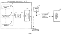
На фиг.1 показана типовая вычислительная система, где процессор 10, который образует центральный процессор ЦП (CPU) вычислительной системы, соединяется с основной памятью 11 шиной 14. Основная память 11 обычно включает в себя запоминающее устройство с произвольной выборкой и обычно называется ЗУПВ (RAM). Потом основная память 11, как правило, соединяется с массовым запоминающим устройством 12, таким, как магнитное или оптическое запоминающее устройство, для массового запоминания (или хранения) информации. Кэш-память 13 (ниже также называемая просто кэшем) соединяется также с шиной 14. Кэш 13 показан расположенным между CPU 11 и основной памятью 11 для того, чтобы привести пример функционального использования и передачи данных, связанных с кэшем 13. Понятно, что действительное физическое размещение кэша 13 может изменяться в зависимости от системы и конфигурации процессора. Кроме того, контроллер кэша 15 показан соединенным с кэшем 13 и шиной 14 для управления работой кэша 13. Работа контроллера кэша, такого, как контроллер 15, известна в технике и, таким образом, на последующих чертежах контроллеры кэша не иллюстрируются. Предполагается, что некоторый(е) контроллер(ы) находится(ятся) под управлением ЦП 10 для управления работой показанного(ых) кэша(ей). Figure 1 shows a typical computing system, where a
При работе вычислительной системы передача информации между памятью 11 и ЦП 10 выполняется посредством доступов (обращений) к памяти от ЦП 10. Когда кэшируемые данные являются легко или быстро доступными для ЦП 10, эти данные сначала размещаются в кэше 13. То есть, когда ЦП 10 обращается к данной информации из памяти 11, он получает информацию из кэша 13. Если запрошенные данные находятся в кэше 13, происходит "результативное обращение". В противном случае следует "промах", и разыскивается распределение кэша для данных. Как практикуется в настоящее время, большая часть доступов (либо загрузка, либо хранение) требует распределения кэша 13. Только не кэшируемые обращения не распределяются в кэше. На фиг.2 показана вычислительная система, использующая компоновку со множеством кэшей. ЦП 10, по-прежнему, соединен с основной памятью 11 посредством шины 14, а память 11 затем соединяется с массовым запоминающим устройством 12. Тем не менее, на примере фиг. 2 показаны две отдельные кэш-памяти 21 и 22. Кэши 21-22 показаны организованными последовательно, и каждый является представителем уровня кэша, называемым кэшем уровня 1 (L1) и кэшем уровня 2 (L2) соответственно. Кроме того, кэш L1 21 показан как часть ЦП 10, в то время как кэш L2 22 показан внешним к ЦП 10. Эта структура приводит пример известной практики размещения кэша L1 на интегральной схеме процессора, в то время как кэши более низкого уровня размещаются внешними к нему, где кэши более низкого уровня находятся дальше от ядра процессора. Фактическое положение различных кэш-памятей является конструктивным выбором или продиктовано конфигурацией процессора. Таким образом, понятно, что кэш L1 мог бы располагаться внешним по отношению к ЦП 10. When the computer system is operating, information is transferred between the
Как правило, ЦП 10 включает исполнительное устройство 23, регистровый файл 24 и блок 25 выборки/декодера. Исполнительное устройство 23 является ядром процессора ЦП 10 для исполнения различных арифметических (или не предусматривающих использование ЗУ) команд процессора. Регистровый файл 24 является набором регистров общего назначения для запоминания (или хранения) различной информации, необходимой для исполнительного устройства 23. Может быть более одного регистрового файла в более современных системах. Блок 25 выборки/декодера выбирает команды из ячейки запоминающего устройства (например, основной памяти 11), содержащей команды программы, которые будут исполняться, и декодирует эти команды для выполнения исполнительным устройством 23. В более современных процессорах, использующих конвейерную архитектуру, будущие команды выбираются с упреждением и декодируются перед тем, как команды действительно необходимы, так что процессор не простаивает в ожидании команд, подлежащих выборке при необходимости. Typically, the
Различные блоки 23-25 ЦП 10 соединяются со структурой внутренних шин 27. Устройство сопряжения шин (BIU) 26 обеспечивает интерфейс для соединения различных блоков ЦП 10 с шиной 14. Как показано на фиг.2, кэш L1 соединяется с внутренней шиной 27 и функционирует как внутренний кэш для ЦП 10. Тем не менее, снова следует подчеркнуть, что кэш L1 мог бы находиться вне ЦП 10 и соединяться с шиной 14. Кэши могут использоваться для данных в кэше, команд или и тех, и других. В некоторых системах кэш L1 фактически разделен на две секции: одна секция для данных, использующих кэш, и другая секция для команд, использующих кэш. Тем не менее, для простоты объяснения различные кэши, изображенные на чертежах, показаны как одиночные кэши с данными, командами и другой информацией, называемой здесь данными. Полагается, что функции блоков, показанных на фиг.2, известны. Кроме того, полагается, что ЦП 10 фактически включает значительно больше компонентов, чем непосредственно показанные компоненты. Таким образом, только те структуры, которые имеют отношение к пониманию сущности данного изобретения, показаны на фиг.2. В одном структурном варианте реализации изобретение используется в системах, имеющих кэши данных. Тем не менее, изобретение применимо к любому типу кэша. The various blocks 23-25 of the
Следует также заметить, что вычислительная система может включать в себя более одного ЦП (как показано пунктирной линией на фиг.2). В такой системе является обычным для нескольких ЦП совместно использовать основную память 11 и/или массовое запоминающее устройство 12. Следовательно, некоторые или все кэши, связанные с вычислительной системой, могут совместно использоваться различными процессорами вычислительной системы. Например, с системой фиг.2 кэш L1 21 каждого процессора мог быть использован только своим процессором, но основная память 11 могла быть использована совместно всеми ЦП системы. К тому же, каждый ЦП имеет связанный внешний кэш L2 22. It should also be noted that a computing system may include more than one CPU (as shown by the dashed line in FIG. 2). In such a system, it is common for several CPUs to share the
Изобретение может быть реализовано на практике в вычислительной системе с одним ЦП или в вычислительной системе с несколькими ЦП. Далее отмечается, что другие типы блоков (отличные от процессоров), которые имеют доступ к памяти, могут функционировать эквивалентно ЦП, описанным здесь, и, следовательно, способны выполнять функции доступа к памяти, подобные описанным ЦП. Например, устройства прямого доступа к памяти (DMA) легко могут получить доступ к памяти, подобно процессорам, описанным здесь. Таким образом, вычислительная система, имеющая один процессор ЦП, но один или более блоков доступа к памяти, работала бы эквивалентно показанной и описанной здесь системе с несколькими процессорами. The invention can be practiced in a computer system with one CPU or in a computer system with multiple CPUs. It is further noted that other types of units (other than processors) that have access to memory can function equivalent to the CPUs described here, and therefore are capable of performing memory access functions similar to those described by the CPUs. For example, direct memory access (DMA) devices can easily access memory, similar to the processors described here. Thus, a computing system having one CPU but one or more memory access blocks would work equivalent to the multi-processor system shown and described here.
Как отмечалось, показаны только два кэша 21-22. Тем не менее, вычислительная система не обязательно ограничивается только двумя уровнями кэша. В настоящее время практикуется использование кэша третьего уровня (L3) в более усовершенствованных системах. Также практикуется иметь последовательную организацию кэш-памятей, так что данные, кэшированные в кэше L1, также кэшируются в кэше L2. Если, возможно, имеется кэш L3, тогда данные, размещенные в кэше L2, обычно размещаются (кэшируются) также в кэше L3. Таким образом, данные, размещенные на отдельном уровне кэша, также кэшируются на всех более высоких уровнях иерархии кэша. As noted, only two caches 21-22 are shown. However, a computing system is not necessarily limited to only two levels of cache. Currently, the practice of using the cache of the third level (L3) in more advanced systems. It is also practiced to have sequential cache organization, so that data cached in L1 cache is also cached in L2 cache. If there may be an L3 cache, then data located in the L2 cache is usually placed (cached) also in the L3 cache. In this way, data located at a separate cache level is also cached at all higher levels of the cache hierarchy.
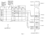
Фиг.3 является блок-схемой, иллюстрирующей один структурный вариант реализации организационной структуры кэш-памяти, в которой используется техника данного изобретения. Вообще имеется "х" наборов данных в структуре кэша, "у" областей на один упомянутый набор (где у≥2), и причем каждая область содержит одну запись данных или одну строку кэша. Изобретение предусматривает фиксирующий бит LRU (наиболее давний по использованию), который показывает, содержит ли какая-либо одна из областей в этом наборе невременные (NT) данные. Если это имеет место, регулярные или псевдо LRU биты будут корректироваться для указания NT данных. Существуют также "z" регулярных или псевдо-LRU битов на один набор. Если не устанавливается фиксирующий бит LRU, регулярные или псевдо-LRU биты указывают на область в наборе в соответствии с используемой техникой наиболее давнего по использованию элемента. Число регулярных или псевдо-LRU битов на набор изменяется в зависимости от числа областей на один набор и используемой (регулярной или псевдо) техники наиболее давнего по использованию элемента (LRU). FIG. 3 is a block diagram illustrating one structural embodiment of an organizational cache structure that utilizes the technique of the present invention. In general, there are “x” data sets in the cache structure, “y” areas per one mentioned set (where y≥2), and each region containing one data record or one cache line. The invention provides for a LRU (oldest used) bit, which indicates whether any one of the areas in this set contains non-temporal (NT) data. If this is the case, regular or pseudo LRU bits will be adjusted to indicate NT data. There are also “z” regular or pseudo-LRU bits per set. If the LRU fix bit is not set, regular or pseudo-LRU bits indicate a region in the set according to the technique used by the oldest element in use. The number of regular or pseudo-LRU bits per set varies depending on the number of areas per set and the used (regular or pseudo) technique of the oldest element (LRU) in use.
В этом варианте реализации показано, что кэш 50 организуется как ассоциативный кэш с набором из четырех областей. На примере фиг.3 показана каждая страница, которая эквивалентна 1/4 размера кэша. В частности, кэш 50 разделяется на четыре области (например, область 0 (52), область 1 (54), область 2 (56) и область 3 (58)) одинакового размера, и основная память 11 (см. также фиг.1 и 2) показана разделенной на страницы (например, страница 0 - страница n). В другом варианте реализации каждая страница может быть больше или меньше размера кэша. Организационная структура кэша 50 (как показано на фиг.3) может использоваться в кэше 13 фиг.1, кэше L1 21 и/или кэше L2 22 фиг.2. In this embodiment, it is shown that the cache 50 is organized as an associative cache with a set of four areas. In the example of FIG. 3, each page is shown that is equivalent to 1/4 of the cache size. In particular, the cache 50 is divided into four regions (for example, region 0 (52), region 1 (54), region 2 (56) and region 3 (58)) of the same size, and the main memory 11 (see also FIG. 1 and 2) is shown paginated (for example, page 0 - page n). In another implementation, each page may be larger or smaller than the cache size. The organizational structure of cache 50 (as shown in FIG. 3) can be used in cache 13 of FIG. 1,
Кэш 50 также включает матрицу из битов наиболее давнего по использованию (LRU) 600-60п, каждый из которых указывает область в наборе с данными наиболее давними по использованию (или NT данными, если используется измененная техника замещения наиболее давнего по использованию элемента). Такая распечатка проводится в соответствии с техникой наиболее давнего по использованию элемента под управлением контроллера кэша 15 для определения, какую запись кэша перезаписать в том случае, если набор кэша полон. Логика замещения наиболее давнего по использованию элемента (не показана) отслеживает положения кэша в наборе, который является наиболее давним по использованию. В одном варианте реализации может использоваться техника замещения наиболее давних по использованию элементов (LRU), которая строго отслеживает алгоритм наиболее давнего по использованию элемента директории. В одном альтернативном варианте реализации используется псевдоалгоритм (LRU), который производит наилучшую попытку в прослеживании наиболее давнего по использованию элемента директории. Для дискуссионных целей биты 600-60п будут называться битами LRU 600-60п, в то время как матрица битов LRU 600-60п будет называться LRU битами 60.Cache 50 also includes a matrix of the most-used (LRU) bits 60 0 -60 p , each of which indicates the area in the data set with the oldest-used data (or NT data, if a modified technique is used to replace the oldest-used element). Such a printout is carried out in accordance with the technique of the oldest element in use under the control of the cache controller 15 to determine which cache entry to overwrite if the cache set is full. The replacement logic of the oldest element in use (not shown) tracks the cache positions in the set that is the oldest in use. In one embodiment, the technique of replacing the oldest elements in use (LRU), which strictly follows the algorithm of the oldest directory element in use, can be used. In one alternative implementation, a pseudo-algorithm (LRU) is used, which makes the best attempt at tracing the oldest directory item in use. For discussion purposes, bits 60 0 -60 p will be called bits LRU 60 0 -60 p , while the matrix of bits LRU 60 0 -60 p will be called LRU bits 60.
Кэш 50 далее включает матрицу фиксирующих битов LRU 700-70п, которые показывают, содержит ли какая-либо из областей 52, 54, 56, 58 в данном наборе данные, которые не должны "засорять" кэш 50 (т.е. данные с редким использованием), как подробно описано в следующих разделах текста описания.The cache 50 further includes a matrix of LRU 70 0 -70 p fixing bits, which indicate whether any of the
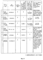
Фиг. 4 является таблицей, иллюстрирующей технику управления кэшем в соответствии с принципами данного изобретения. Изобретение использует матрицу фиксирующих битов LRU 700-70п для указания, являются ли какие-либо соответствующие хранимые в кэше данные текущими или невременными, а по существу, должна ли первая запись заменяться при неудачном обращении в кэш к соответствующему набору данных. В одном варианте реализации фиксирующий бит LRU 70, когда установлен на 1, указывает, что соответствующий набор данных имеет запись, которая является невременной. Если фиксирующий бит LRU 70 сбрасывается при удачном (результативном) обращении к кэшу при временной команде, соответствующий(ие) бит(ы) LRU 60 корректируется(ются) в соответствии с применяемой техникой замещения наиболее давних по использованию элементов (см. поз. 1 фиг.4), и связанный фиксирующий бит LRU не корректируется. Тем не менее, если фиксирующий бит LRU 70 уже установлен на 1 (указывая, что соответствующий набор данных имеет невременную команду), фиксирующий бит 70 LRU не корректируется, и бит 60 LRU не корректируется (см. поз. 2).FIG. 4 is a table illustrating a cache management technique in accordance with the principles of the present invention. The invention uses a matrix of fixing bits LRU 70 0 -70 p to indicate whether any relevant data stored in the cache is current or temporary, and essentially whether the first record should be replaced when the cache is unsuccessfully accessed by the corresponding data set. In one embodiment, the fix bit LRU 70, when set to 1, indicates that the corresponding data set has a record that is non-transitory. If the LRU 70 latch bit is reset when the cache is accessed successfully (efficiently) with a temporary command, the corresponding LRU 60 bit (s) are corrected (s) in accordance with the technique used to replace the oldest elements in use (see
В случае результативного обращения к кэшу при невременной команде бит LRU 60 и фиксирующий бит LRU 70 не корректируются безотносительно к статусу фиксирующего бита LRU 70 (см. поз.3). В альтернативном варианте реализации при управлении посредством режимного бита в управляющем регистре в контроллере кэша L1, результативные обращения к кэшу при текущих или невременных командах вынуждают биты LRU указывать область, к которой имело место результативное обращение (см. позицию 4). Кроме того, фиксирующий бит LRU 70 устанавливается на 1. В этом варианте реализации результативное обращение к данным при текущей или невременной команде должно быть первым, подлежащим замене при неудачном обращении в кэш к соответствующему набору данных. If the cache is accessed efficiently with an untimely instruction, the LRU 60 bit and the LRU 70 fix bit are not corrected regardless of the status of the LRU 70 fix bit (see pos. 3). In an alternative implementation, when controlled by a mode bit in the control register in the L1 cache controller, effective cache accesses with current or non-temporary instructions force the LRU bits to indicate the area to which the effective address has occurred (see position 4). In addition, the latch bit LRU 70 is set to 1. In this embodiment, the effective data access with the current or non-temporary command should be the first to be replaced if the cache is not accessed by the corresponding data set.
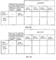
Если происходит неудачное обращение в кэш при временной команде, фиксирующий бит LRU сбрасывается, и корректируется бит LRU 60 (поз. 5), исходя из техники псевдо-LRU. Тем не менее, при неудачном обращении в кэш при текущей или невременной команде фиксирующий бит LRU 70 устанавливается на 1, и соответствующий бит LRU 60 не корректируется (поз. 6). If a cache failure occurs during a temporary command, the LRU fix bit is reset and the LRU 60 bit (pos. 5) is adjusted based on the pseudo-LRU technique. However, if the cache is unsuccessfully accessed with a current or temporary command, the LRU 70 fix bit is set to 1, and the corresponding LRU 60 bit is not corrected (pos. 6).
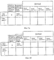
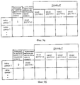
Теперь будут обсуждены примеры каждой из позиций, приведенных в таблице фиг.4. На фиг.5а и 5б проиллюстрирован один пример организации кэш-памяти до и после удачных обращений временной команды в область 2 для набора 0 кэша. Этот пример соответствует поз. 1 фиг. 4. Здесь фиксирующий бит LRU 700 предварительно был сброшен для набора 0 кэша и, так как к набору 0 кэша было результативное обращение временной командой, фиксирующий бит LRU 700 не корректируется. Тем не менее, бит LRU 600 корректируется в соответствии с используемой техникой LRU. В этом примере предполагается, что техника псевдо-LRU показывает, что область 3 является наиболее давней по использованию записью.Now will be discussed examples of each of the items shown in the table of figure 4. On figa and 5b illustrates one example of the organization of the cache before and after the successful calls of the temporary team in
На фиг.6а и 6б проиллюстрирован другой пример организации кэш-памяти до и после результативных обращений временной команды в область 2 для набора 0 кэша. Этот пример соответствует поз. 2 фиг.4. Здесь фиксирующий LRU бит 700 прежде был установлен для набора 0 кэша, указывая, что соответствующий набор содержит невременные данные. Соответственно ни фиксирующий бит LRU 700, ни бит LRU 600 не корректируются.On figa and 6b illustrates another example of the organization of the cache before and after the effective accesses of the temporary command in
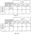
На фиг. 7а-7г проиллюстрирован пример организации кэш-памяти до и после результативных обращений невременной команды в область 2 для набора 0 кэша. Этот пример соответствует поз. 3 фиг.4 и может использоваться при установке режимного бита, расположенного в контроллере кэша L1, на нуль (см. фиг.4). В первом случае (фиг.7а и 7б) фиксирующий бит LRU 700 прежде был сброшен для набора 0 кэша. В этом варианте реализации невременное результативное обращение к кэшу не корректирует фиксирующий бит LRU 70. Соответственно, так как к набору 0 кэша имело место результативное обращение согласно невременной команде, ни фиксирующий бит LRU 700, ни бит LRU 600 не корректируются. Во втором случае (фиг.7в и 7г) фиксирующий бит LRU 700 предварительно был установлен для набора 0 кэша, указывая на то, что соответствующий набор содержит невременные данные. Соответственно ни фиксирующий бит LRU 700, ни бит LRU 600 не корректируются.In FIG. 7a-7g illustrate an example of organizing a cache before and after successful calls of a non-temporary command to
На фиг. 8а-8г показан другой пример организации кэш-памяти до и после результативных обращений невременной команды к набору 0 кэша. Этот пример соответствует поз. 4 фиг.4 и может быть реализован при установке режимного бита, расположенного в контроллере кэша L1, на единицу (см. фиг.4). В первом случае (фиг.8а и 8б) фиксирующий бит LRU 70о прежде был сброшен для набора 0 кэша. В этом примере альтернативного варианта реализации примера, показанного на фиг.7а-7г, невременное результативное обращение к кэшу корректирует фиксирующий бит LRU 70. Соответственно, как показано на фиг.8а, так как к набору 0 кэша имело место результативное обращение согласно невременной команде, фиксирующий бит LRU 700 корректируется (устанавливается на 1), как показано на фиг.8б. Кроме того, биты LRU 600 корректируются для указания области, к которой имело место результативное обращение. В случае, когда фиксирующий бит LRU 700 прежде был установлен для набора 0 кэша (фиг.8в и 8г), фиксирующий бит LRU 700 остается установленным на 1. Кроме того, биты LRU 600 заставляют указывать область в наборе, к которой имело место результативное обращение.In FIG. 8a-8g show another example of cache organization before and after successful calls of a non-temporary command to
На фиг.9а и 9б проиллюстрирован один пример организации кэш-памяти до и после неудачного обращения временной команды к набору 0 кэша. Этот пример соответствует позиции 5 фиг.4. Здесь фиксирующий бит LRU 700 ранее был установлен для набора 0 кэша, а так как имеет место неудачное обращение временной команды, указывающей на набор 0, фиксирующий бит LRU 700 сбрасывается для этого набора после замены временного неудачного обращения к кэшу. Тем не менее, бит LRU 600 корректируется в соответствии с используемой техникой LRU. В этом примере техника псевдо-LRU показывает, что область 3 является наиболее давней по использованию записью.On figa and 9b illustrates one example of the organization of the cache before and after the failure of the temporary command to the set of 0 cache. This example corresponds to position 5 of figure 4. Here, the LRU 70 0 latch bit was previously set for cache set 0, and since there is an unsuccessful reversal of a temporary instruction pointing to set 0, the LRU 70 0 latch bit is reset for this set after replacing a temporary cache failure. However, the LRU 60 0 bit is adjusted according to the LRU technique used. In this example, the pseudo-LRU technique shows that region 3 is the oldest record used.
На фиг.10а-10б проиллюстрирован пример организации кэш-памяти до и после неудачного обращения невременной команды к набору 0 кэша. Этот пример соответствует поз. 6 фиг.4. В этом случае фиксирующий бит LRU 700 ранее был сброшен для набора 0 кэша. Так как имеется невременное неудачное обращение к набору 0 кэша, устанавливается фиксирующий бит LRU 700, и биты LRU 600 остаются теми же самыми для того, чтобы указать на невременные данные в соответствующем наборе 0.On figa-10b illustrates an example of the organization of the cache before and after an unsuccessful appeal of a non-temporary command to a set of 0 cache. This example corresponds to pos. 6 of Fig. 4. In this case, the LRU 70 0 latch bit was previously reset to set
При реализации устройства и способа данного изобретения обеспечивается совместно используемая структура кэша для управления временными и невременными командами, которая сводит к минимуму "засорение" данных в кэше или иерархии кэша. Реализация данного изобретения также устраняет необходимость в использовании отдельного буфера, реализация которого становится более эффективной с точки зрения как стоимости, так и функциональных характеристик. When implementing the device and method of the present invention, a shared cache structure is provided for managing temporary and non-temporal instructions, which minimizes data clogging in the cache or cache hierarchy. The implementation of the present invention also eliminates the need for a separate buffer, the implementation of which becomes more efficient in terms of both cost and functional characteristics.
Данное изобретение может быть реализовано в других специфических формах без отступления от его сути или существенных характеристик. Описанные варианты реализации следует рассматривать во всех аспектах только как иллюстративные, а неограничивающие объема патентных притязаний, определяемого приложенной формулой изобретения, а не вышеизложенным текстом описания. Все изменения в формах и деталях возможны, не отступая от сути и объема патентных притязаний настоящего изобретения, This invention can be implemented in other specific forms without departing from its essence or essential characteristics. The described implementation options should be considered in all aspects only as illustrative and not limiting the scope of patent claims defined by the attached claims, and not the foregoing description text. All changes in the forms and details are possible without departing from the essence and scope of patent claims of the present invention,
Claims (24)
Applications Claiming Priority (2)
| Application Number | Priority Date | Filing Date | Title |
|---|---|---|---|
| US09/053,386 US6202129B1 (en) | 1998-03-31 | 1998-03-31 | Shared cache structure for temporal and non-temporal information using indicative bits |
| US09/053,386 | 1998-03-31 |
Publications (2)
| Publication Number | Publication Date |
|---|---|
| RU2000127102A RU2000127102A (en) | 2002-09-20 |
| RU2212704C2 true RU2212704C2 (en) | 2003-09-20 |
Family
ID=21983863
Family Applications (1)
| Application Number | Title | Priority Date | Filing Date |
|---|---|---|---|
| RU2000127102/09A RU2212704C2 (en) | 1998-03-31 | 1999-03-24 | Shared cache structure for timing and non-timing commands |
Country Status (10)
| Country | Link |
|---|---|
| US (2) | US6202129B1 (en) |
| EP (1) | EP1066566B1 (en) |
| JP (1) | JP4486750B2 (en) |
| KR (1) | KR100389549B1 (en) |
| CN (1) | CN1230750C (en) |
| AU (1) | AU3364599A (en) |
| BR (1) | BR9909295A (en) |
| RU (1) | RU2212704C2 (en) |
| TW (1) | TW573252B (en) |
| WO (1) | WO1999050752A1 (en) |
Cited By (3)
| Publication number | Priority date | Publication date | Assignee | Title |
|---|---|---|---|---|
| US8078803B2 (en) | 2008-01-30 | 2011-12-13 | Qualcomm Incorporated | Apparatus and methods to reduce castouts in a multi-level cache hierarchy |
| RU2527736C2 (en) * | 2009-12-16 | 2014-09-10 | Телефонактиеболагет Л М Эрикссон (Пабл) | Method, server, computer programme and computer programme product for caching |
| RU2606551C2 (en) * | 2008-07-23 | 2017-01-10 | Майкро Моушн, Инк. | Processing system with external memory access control |
Families Citing this family (65)
| Publication number | Priority date | Publication date | Assignee | Title |
|---|---|---|---|---|
| US5978379A (en) | 1997-01-23 | 1999-11-02 | Gadzoox Networks, Inc. | Fiber channel learning bridge, learning half bridge, and protocol |
| US6202129B1 (en) * | 1998-03-31 | 2001-03-13 | Intel Corporation | Shared cache structure for temporal and non-temporal information using indicative bits |
| US6216215B1 (en) | 1998-04-02 | 2001-04-10 | Intel Corporation | Method and apparatus for senior loads |
| US6542966B1 (en) * | 1998-07-16 | 2003-04-01 | Intel Corporation | Method and apparatus for managing temporal and non-temporal data in a single cache structure |
| US7430171B2 (en) | 1998-11-19 | 2008-09-30 | Broadcom Corporation | Fibre channel arbitrated loop bufferless switch circuitry to increase bandwidth without significant increase in cost |
| US6560677B1 (en) * | 1999-05-04 | 2003-05-06 | International Business Machines Corporation | Methods, cache memories, systems and computer program products for storing transient, normal, and locked entries in an associative cache memory |
| US6728835B1 (en) * | 2000-08-30 | 2004-04-27 | Unisys Corporation | Leaky cache mechanism |
| US6681295B1 (en) * | 2000-08-31 | 2004-01-20 | Hewlett-Packard Development Company, L.P. | Fast lane prefetching |
| US6598124B1 (en) * | 2000-09-29 | 2003-07-22 | Sun Microsystems, Inc. | System and method for identifying streaming-data |
| US6578111B1 (en) * | 2000-09-29 | 2003-06-10 | Sun Microsystems, Inc. | Cache memory system and method for managing streaming-data |
| US6668307B1 (en) * | 2000-09-29 | 2003-12-23 | Sun Microsystems, Inc. | System and method for a software controlled cache |
| WO2002027498A2 (en) * | 2000-09-29 | 2002-04-04 | Sun Microsystems, Inc. | System and method for identifying and managing streaming-data |
| US6766413B2 (en) * | 2001-03-01 | 2004-07-20 | Stratus Technologies Bermuda Ltd. | Systems and methods for caching with file-level granularity |
| US7287649B2 (en) * | 2001-05-18 | 2007-10-30 | Broadcom Corporation | System on a chip for packet processing |
| US6766389B2 (en) * | 2001-05-18 | 2004-07-20 | Broadcom Corporation | System on a chip for networking |
| US6574708B2 (en) | 2001-05-18 | 2003-06-03 | Broadcom Corporation | Source controlled cache allocation |
| US7239636B2 (en) | 2001-07-23 | 2007-07-03 | Broadcom Corporation | Multiple virtual channels for use in network devices |
| US6823426B2 (en) * | 2001-12-20 | 2004-11-23 | Intel Corporation | System and method of data replacement in cache ways |
| US7328328B2 (en) * | 2002-02-19 | 2008-02-05 | Ip-First, Llc | Non-temporal memory reference control mechanism |
| US7295555B2 (en) | 2002-03-08 | 2007-11-13 | Broadcom Corporation | System and method for identifying upper layer protocol message boundaries |
| US7114043B2 (en) * | 2002-05-15 | 2006-09-26 | Broadcom Corporation | Ambiguous virtual channels |
| US7269709B2 (en) * | 2002-05-15 | 2007-09-11 | Broadcom Corporation | Memory controller configurable to allow bandwidth/latency tradeoff |
| US7266587B2 (en) | 2002-05-15 | 2007-09-04 | Broadcom Corporation | System having interfaces, switch, and memory bridge for CC-NUMA operation |
| US7073030B2 (en) | 2002-05-22 | 2006-07-04 | International Business Machines Corporation | Method and apparatus providing non level one information caching using prefetch to increase a hit ratio |
| US7035979B2 (en) * | 2002-05-22 | 2006-04-25 | International Business Machines Corporation | Method and apparatus for optimizing cache hit ratio in non L1 caches |
| US6904501B1 (en) * | 2002-06-17 | 2005-06-07 | Silicon Graphics, Inc. | Cache memory for identifying locked and least recently used storage locations |
| US7346701B2 (en) | 2002-08-30 | 2008-03-18 | Broadcom Corporation | System and method for TCP offload |
| US7934021B2 (en) | 2002-08-29 | 2011-04-26 | Broadcom Corporation | System and method for network interfacing |
| US7411959B2 (en) | 2002-08-30 | 2008-08-12 | Broadcom Corporation | System and method for handling out-of-order frames |
| US7313623B2 (en) | 2002-08-30 | 2007-12-25 | Broadcom Corporation | System and method for TCP/IP offload independent of bandwidth delay product |
| US8180928B2 (en) | 2002-08-30 | 2012-05-15 | Broadcom Corporation | Method and system for supporting read operations with CRC for iSCSI and iSCSI chimney |
| US7512498B2 (en) * | 2002-12-31 | 2009-03-31 | Intel Corporation | Streaming processing of biological sequence matching |
| WO2005050455A1 (en) * | 2003-11-18 | 2005-06-02 | Matsushita Electric Industrial Co., Ltd. | Cache memory and control method thereof |
| US7321954B2 (en) * | 2004-08-11 | 2008-01-22 | International Business Machines Corporation | Method for software controllable dynamically lockable cache line replacement system |
| US20060101208A1 (en) * | 2004-11-09 | 2006-05-11 | Intel Corporation | Method and apparatus for handling non-temporal memory accesses in a cache |
| US7356650B1 (en) * | 2005-06-17 | 2008-04-08 | Unisys Corporation | Cache apparatus and method for accesses lacking locality |
| US7437510B2 (en) * | 2005-09-30 | 2008-10-14 | Intel Corporation | Instruction-assisted cache management for efficient use of cache and memory |
| US7624257B2 (en) * | 2005-11-30 | 2009-11-24 | International Business Machines Corporation | Digital data processing apparatus having hardware multithreading support including a register set reserved for special class threads |
| US20070150658A1 (en) * | 2005-12-28 | 2007-06-28 | Jaideep Moses | Pinning locks in shared cache |
| US8527713B2 (en) * | 2006-01-31 | 2013-09-03 | Qualcomm Incorporated | Cache locking without interference from normal allocations |
| GB0603552D0 (en) | 2006-02-22 | 2006-04-05 | Advanced Risc Mach Ltd | Cache management within a data processing apparatus |
| JP4369524B2 (en) * | 2006-02-27 | 2009-11-25 | 富士通株式会社 | LRU control device and LRU control program |
| US20080147989A1 (en) * | 2006-12-14 | 2008-06-19 | Arm Limited | Lockdown control of a multi-way set associative cache memory |
| US7793049B2 (en) * | 2007-10-30 | 2010-09-07 | International Business Machines Corporation | Mechanism for data cache replacement based on region policies |
| US8108614B2 (en) * | 2007-12-31 | 2012-01-31 | Eric Sprangle | Mechanism for effectively caching streaming and non-streaming data patterns |
| US8364898B2 (en) * | 2009-01-23 | 2013-01-29 | International Business Machines Corporation | Optimizing a cache back invalidation policy |
| US8312219B2 (en) | 2009-03-02 | 2012-11-13 | International Business Machines Corporation | Hybrid caching techniques and garbage collection using hybrid caching techniques |
| US8521963B1 (en) * | 2009-09-21 | 2013-08-27 | Tilera Corporation | Managing cache coherence |
| US9323527B2 (en) * | 2010-10-15 | 2016-04-26 | International Business Machines Corporation | Performance of emerging applications in a virtualized environment using transient instruction streams |
| EP3364304B1 (en) | 2011-09-30 | 2022-06-15 | INTEL Corporation | Memory channel that supports near memory and far memory access |
| US9378142B2 (en) | 2011-09-30 | 2016-06-28 | Intel Corporation | Apparatus and method for implementing a multi-level memory hierarchy having different operating modes |
| EP2761480A4 (en) | 2011-09-30 | 2015-06-24 | Intel Corp | Apparatus and method for implementing a multi-level memory hierarchy over common memory channels |
| US9600416B2 (en) | 2011-09-30 | 2017-03-21 | Intel Corporation | Apparatus and method for implementing a multi-level memory hierarchy |
| JPWO2013080426A1 (en) * | 2011-12-01 | 2015-04-27 | パナソニックIpマネジメント株式会社 | Integrated circuit device having structure considering heat, three-dimensional integrated circuit, three-dimensional processor device, and process scheduler |
| US9519549B2 (en) * | 2012-01-11 | 2016-12-13 | International Business Machines Corporation | Data storage backup with lessened cache pollution |
| US8874852B2 (en) | 2012-03-28 | 2014-10-28 | International Business Machines Corporation | Data cache block deallocate requests in a multi-level cache hierarchy |
| US8856455B2 (en) | 2012-03-28 | 2014-10-07 | International Business Machines Corporation | Data cache block deallocate requests |
| CN103577480B (en) * | 2012-08-07 | 2017-05-31 | 中国银联股份有限公司 | A kind of parameter division system and its method, a kind of transaction processing system and its method |
| US9558121B2 (en) * | 2012-12-28 | 2017-01-31 | Intel Corporation | Two-level cache locking mechanism |
| US9256539B2 (en) | 2013-03-07 | 2016-02-09 | Lenovo Enterprise Solutions (Singapore) Pte. Ltd. | Sharing cache in a computing system |
| WO2014142867A1 (en) | 2013-03-14 | 2014-09-18 | Intel Corporation | Power efficient level one data cache access with pre-validated tags |
| US20150095586A1 (en) * | 2013-09-30 | 2015-04-02 | Advanced Micro Devices , Inc. | Storing non-temporal cache data |
| US11580125B2 (en) * | 2015-05-08 | 2023-02-14 | Adp, Inc. | Information system with temporal data |
| US10379827B2 (en) | 2016-12-29 | 2019-08-13 | Intel Corporation | Automatic identification and generation of non-temporal store and load operations in a dynamic optimization environment |
| US11681627B1 (en) * | 2021-10-18 | 2023-06-20 | Meta Platforms Technologies, Llc | Distributed temporal cache for Systems on a Chip |
Family Cites Families (33)
| Publication number | Priority date | Publication date | Assignee | Title |
|---|---|---|---|---|
| JPS5119453A (en) * | 1974-08-08 | 1976-02-16 | Fujitsu Ltd | Patsufua memoriseigyohoshiki |
| JPS5534336A (en) * | 1978-08-31 | 1980-03-10 | Fujitsu Ltd | Buffer memory control method |
| JPS58159285A (en) * | 1982-03-17 | 1983-09-21 | Nec Corp | Buffer memory control system |
| JPH01133162A (en) * | 1987-11-18 | 1989-05-25 | Fujitsu Ltd | Cache memory control system |
| US4905141A (en) | 1988-10-25 | 1990-02-27 | International Business Machines Corporation | Partitioned cache memory with partition look-aside table (PLAT) for early partition assignment identification |
| JPH0358151A (en) * | 1989-07-26 | 1991-03-13 | Nec Corp | Cache memory device |
| JPH0358252A (en) * | 1989-07-27 | 1991-03-13 | Nec Corp | Cache memory controller |
| JPH041838A (en) * | 1990-04-18 | 1992-01-07 | Nec Corp | Cache memory control circuit |
| JPH04215151A (en) * | 1990-12-13 | 1992-08-05 | Nec Commun Syst Ltd | Cache control system |
| EP0496439B1 (en) * | 1991-01-15 | 1998-01-21 | Koninklijke Philips Electronics N.V. | Computer system with multi-buffer data cache and method therefor |
| GB2255211B (en) * | 1991-04-25 | 1995-05-17 | Intel Corp | LRU pointer updating in a controller for two-way set associative cache |
| GB2256512B (en) * | 1991-06-04 | 1995-03-15 | Intel Corp | Second level cache controller unit and system |
| JPH05165726A (en) * | 1991-12-12 | 1993-07-02 | Nec Corp | Data processor |
| JPH05233454A (en) * | 1992-02-24 | 1993-09-10 | Hitachi Ltd | Cache memory device |
| US5353425A (en) * | 1992-04-29 | 1994-10-04 | Sun Microsystems, Inc. | Methods and apparatus for implementing a pseudo-LRU cache memory replacement scheme with a locking feature |
| US5471605A (en) * | 1992-08-27 | 1995-11-28 | Intel Corporation | Apparatus for updating a multi-way set associative cache memory status array |
| US5434992A (en) | 1992-09-04 | 1995-07-18 | International Business Machines Corporation | Method and means for dynamically partitioning cache into a global and data type subcache hierarchy from a real time reference trace |
| US5493667A (en) * | 1993-02-09 | 1996-02-20 | Intel Corporation | Apparatus and method for an instruction cache locking scheme |
| JPH06348595A (en) * | 1993-06-07 | 1994-12-22 | Hitachi Ltd | Cache device |
| JPH07281957A (en) * | 1994-04-15 | 1995-10-27 | Hitachi Ltd | Cache storage and access instruction generation method |
| US5826052A (en) | 1994-04-29 | 1998-10-20 | Advanced Micro Devices, Inc. | Method and apparatus for concurrent access to multiple physical caches |
| JPH07334428A (en) * | 1994-06-14 | 1995-12-22 | Toshiba Corp | Cache memory |
| US5584014A (en) * | 1994-12-20 | 1996-12-10 | Sun Microsystems, Inc. | Apparatus and method to preserve data in a set associative memory device |
| US5701426A (en) * | 1995-03-31 | 1997-12-23 | Bull Information Systems Inc. | Data processing system and method using cache miss address prediction and forced LRU status in a cache memory to improve cache hit ratio |
| US5845317A (en) * | 1995-11-17 | 1998-12-01 | Micron Technology, Inc. | Multi-way cache expansion circuit architecture |
| GB2311880A (en) * | 1996-04-03 | 1997-10-08 | Advanced Risc Mach Ltd | Partitioned cache memory |
| US5829025A (en) * | 1996-12-17 | 1998-10-27 | Intel Corporation | Computer system and method of allocating cache memories in a multilevel cache hierarchy utilizing a locality hint within an instruction |
| JPH10207767A (en) * | 1997-01-16 | 1998-08-07 | Toshiba Corp | Cache memory with lock function and microprocessor equipped with cache memory |
| US6434671B2 (en) * | 1997-09-30 | 2002-08-13 | Intel Corporation | Software-controlled cache memory compartmentalization |
| US6223258B1 (en) * | 1998-03-31 | 2001-04-24 | Intel Corporation | Method and apparatus for implementing non-temporal loads |
| US6202129B1 (en) * | 1998-03-31 | 2001-03-13 | Intel Corporation | Shared cache structure for temporal and non-temporal information using indicative bits |
| US6105111A (en) * | 1998-03-31 | 2000-08-15 | Intel Corporation | Method and apparatus for providing a cache management technique |
| US6205520B1 (en) * | 1998-03-31 | 2001-03-20 | Intel Corporation | Method and apparatus for implementing non-temporal stores |
-
1998
- 1998-03-31 US US09/053,386 patent/US6202129B1/en not_active Expired - Lifetime
-
1999
- 1999-03-24 RU RU2000127102/09A patent/RU2212704C2/en not_active IP Right Cessation
- 1999-03-24 BR BR9909295-6A patent/BR9909295A/en not_active Application Discontinuation
- 1999-03-24 AU AU33645/99A patent/AU3364599A/en not_active Abandoned
- 1999-03-24 KR KR10-2000-7010799A patent/KR100389549B1/en not_active IP Right Cessation
- 1999-03-24 CN CNB998047333A patent/CN1230750C/en not_active Expired - Lifetime
- 1999-03-24 JP JP2000541596A patent/JP4486750B2/en not_active Expired - Fee Related
- 1999-03-24 EP EP99915030A patent/EP1066566B1/en not_active Expired - Lifetime
- 1999-03-24 WO PCT/US1999/006501 patent/WO1999050752A1/en active IP Right Grant
- 1999-03-31 TW TW88105070A patent/TW573252B/en not_active IP Right Cessation
-
2001
- 2001-03-09 US US09/803,357 patent/US6584547B2/en not_active Expired - Lifetime
Cited By (4)
| Publication number | Priority date | Publication date | Assignee | Title |
|---|---|---|---|---|
| US8078803B2 (en) | 2008-01-30 | 2011-12-13 | Qualcomm Incorporated | Apparatus and methods to reduce castouts in a multi-level cache hierarchy |
| US8386716B2 (en) | 2008-01-30 | 2013-02-26 | Qualcomm Incorporated | Apparatus and methods to reduce castouts in a multi-level cache hierarchy |
| RU2606551C2 (en) * | 2008-07-23 | 2017-01-10 | Майкро Моушн, Инк. | Processing system with external memory access control |
| RU2527736C2 (en) * | 2009-12-16 | 2014-09-10 | Телефонактиеболагет Л М Эрикссон (Пабл) | Method, server, computer programme and computer programme product for caching |
Also Published As
| Publication number | Publication date |
|---|---|
| WO1999050752A9 (en) | 2000-05-25 |
| US6584547B2 (en) | 2003-06-24 |
| EP1066566A4 (en) | 2002-10-23 |
| JP4486750B2 (en) | 2010-06-23 |
| KR20010042262A (en) | 2001-05-25 |
| CN1230750C (en) | 2005-12-07 |
| JP2002510085A (en) | 2002-04-02 |
| WO1999050752A1 (en) | 1999-10-07 |
| US6202129B1 (en) | 2001-03-13 |
| EP1066566A1 (en) | 2001-01-10 |
| BR9909295A (en) | 2000-12-05 |
| AU3364599A (en) | 1999-10-18 |
| CN1295687A (en) | 2001-05-16 |
| US20020007441A1 (en) | 2002-01-17 |
| TW573252B (en) | 2004-01-21 |
| EP1066566B1 (en) | 2006-11-02 |
| KR100389549B1 (en) | 2003-06-27 |
Similar Documents
| Publication | Publication Date | Title |
|---|---|---|
| RU2212704C2 (en) | Shared cache structure for timing and non-timing commands | |
| US4774654A (en) | Apparatus and method for prefetching subblocks from a low speed memory to a high speed memory of a memory hierarchy depending upon state of replacing bit in the low speed memory | |
| US5465342A (en) | Dynamically adaptive set associativity for cache memories | |
| US5091851A (en) | Fast multiple-word accesses from a multi-way set-associative cache memory | |
| US6138213A (en) | Cache including a prefetch way for storing prefetch cache lines and configured to move a prefetched cache line to a non-prefetch way upon access to the prefetched cache line | |
| JP3016575B2 (en) | Multiple cache memory access methods | |
| US6185660B1 (en) | Pending access queue for providing data to a target register during an intermediate pipeline phase after a computer cache miss | |
| US8725987B2 (en) | Cache memory system including selectively accessible pre-fetch memory for pre-fetch of variable size data | |
| US20070204107A1 (en) | Cache memory background preprocessing | |
| US6292871B1 (en) | Loading accessed data from a prefetch buffer to a least recently used position in a cache | |
| US20150149733A1 (en) | Supporting speculative modification in a data cache | |
| JP4298800B2 (en) | Prefetch management in cache memory | |
| US5960463A (en) | Cache controller with table walk logic tightly coupled to second level access logic | |
| JP5039913B2 (en) | Direct storage using a locking cache | |
| US20020169935A1 (en) | System of and method for memory arbitration using multiple queues | |
| US7237067B2 (en) | Managing a multi-way associative cache | |
| JP3262519B2 (en) | Method and system for enhancing processor memory performance by removing old lines in second level cache | |
| US5471602A (en) | System and method of scoreboarding individual cache line segments | |
| US5822764A (en) | Method and circuit for efficiently replacing invalid locked portions of a cache with valid data | |
| US5287512A (en) | Computer memory system and method for cleaning data elements | |
| US6240487B1 (en) | Integrated cache buffers | |
| US20060095668A1 (en) | Method for processor to use locking cache as part of system memory | |
| JP2000047942A (en) | Device and method for controlling cache memory | |
| EP0470737A1 (en) | Cache memory operating method and structure | |
| JPH0342744A (en) | Computing system with cash-memory and method of controlling cash-memory |
Legal Events
| Date | Code | Title | Description |
|---|---|---|---|
| MM4A | The patent is invalid due to non-payment of fees |
Effective date: 20170325 |