RU2138930C1 - Method for manufacturing of conducting circuit on substrate, conducting circuit on substrate and device for manufacturing of flexible conducting circuit - Google Patents
Method for manufacturing of conducting circuit on substrate, conducting circuit on substrate and device for manufacturing of flexible conducting circuit Download PDFInfo
- Publication number
- RU2138930C1 RU2138930C1 RU94040379A RU94040379A RU2138930C1 RU 2138930 C1 RU2138930 C1 RU 2138930C1 RU 94040379 A RU94040379 A RU 94040379A RU 94040379 A RU94040379 A RU 94040379A RU 2138930 C1 RU2138930 C1 RU 2138930C1
- Authority
- RU
- Russia
- Prior art keywords
- sheet
- electrically conductive
- conductive
- layer
- circuit
- Prior art date
Links
Images

Classifications
-
- H—ELECTRICITY
- H05—ELECTRIC TECHNIQUES NOT OTHERWISE PROVIDED FOR
- H05K—PRINTED CIRCUITS; CASINGS OR CONSTRUCTIONAL DETAILS OF ELECTRIC APPARATUS; MANUFACTURE OF ASSEMBLAGES OF ELECTRICAL COMPONENTS
- H05K7/00—Constructional details common to different types of electric apparatus
- H05K7/14—Mounting supporting structure in casing or on frame or rack
- H05K7/1438—Back panels or connecting means therefor; Terminals; Coding means to avoid wrong insertion
- H05K7/1447—External wirings; Wiring ducts; Laying cables
- H05K7/1451—External wirings; Wiring ducts; Laying cables with connections between circuit boards or units
-
- H—ELECTRICITY
- H05—ELECTRIC TECHNIQUES NOT OTHERWISE PROVIDED FOR
- H05K—PRINTED CIRCUITS; CASINGS OR CONSTRUCTIONAL DETAILS OF ELECTRIC APPARATUS; MANUFACTURE OF ASSEMBLAGES OF ELECTRICAL COMPONENTS
- H05K1/00—Printed circuits
-
- H—ELECTRICITY
- H01—ELECTRIC ELEMENTS
- H01R—ELECTRICALLY-CONDUCTIVE CONNECTIONS; STRUCTURAL ASSOCIATIONS OF A PLURALITY OF MUTUALLY-INSULATED ELECTRICAL CONNECTING ELEMENTS; COUPLING DEVICES; CURRENT COLLECTORS
- H01R31/00—Coupling parts supported only by co-operation with counterpart
-
- H—ELECTRICITY
- H05—ELECTRIC TECHNIQUES NOT OTHERWISE PROVIDED FOR
- H05K—PRINTED CIRCUITS; CASINGS OR CONSTRUCTIONAL DETAILS OF ELECTRIC APPARATUS; MANUFACTURE OF ASSEMBLAGES OF ELECTRICAL COMPONENTS
- H05K3/00—Apparatus or processes for manufacturing printed circuits
- H05K3/02—Apparatus or processes for manufacturing printed circuits in which the conductive material is applied to the surface of the insulating support and is thereafter removed from such areas of the surface which are not intended for current conducting or shielding
- H05K3/04—Apparatus or processes for manufacturing printed circuits in which the conductive material is applied to the surface of the insulating support and is thereafter removed from such areas of the surface which are not intended for current conducting or shielding the conductive material being removed mechanically, e.g. by punching
- H05K3/045—Apparatus or processes for manufacturing printed circuits in which the conductive material is applied to the surface of the insulating support and is thereafter removed from such areas of the surface which are not intended for current conducting or shielding the conductive material being removed mechanically, e.g. by punching by making a conductive layer having a relief pattern, followed by abrading of the raised portions
-
- H—ELECTRICITY
- H05—ELECTRIC TECHNIQUES NOT OTHERWISE PROVIDED FOR
- H05K—PRINTED CIRCUITS; CASINGS OR CONSTRUCTIONAL DETAILS OF ELECTRIC APPARATUS; MANUFACTURE OF ASSEMBLAGES OF ELECTRICAL COMPONENTS
- H05K3/00—Apparatus or processes for manufacturing printed circuits
- H05K3/46—Manufacturing multilayer circuits
- H05K3/4611—Manufacturing multilayer circuits by laminating two or more circuit boards
- H05K3/4614—Manufacturing multilayer circuits by laminating two or more circuit boards the electrical connections between the circuit boards being made during lamination
-
- H—ELECTRICITY
- H05—ELECTRIC TECHNIQUES NOT OTHERWISE PROVIDED FOR
- H05K—PRINTED CIRCUITS; CASINGS OR CONSTRUCTIONAL DETAILS OF ELECTRIC APPARATUS; MANUFACTURE OF ASSEMBLAGES OF ELECTRICAL COMPONENTS
- H05K9/00—Screening of apparatus or components against electric or magnetic fields
- H05K9/0007—Casings
- H05K9/002—Casings with localised screening
- H05K9/0039—Galvanic coupling of ground layer on printed circuit board [PCB] to conductive casing
-
- H—ELECTRICITY
- H05—ELECTRIC TECHNIQUES NOT OTHERWISE PROVIDED FOR
- H05K—PRINTED CIRCUITS; CASINGS OR CONSTRUCTIONAL DETAILS OF ELECTRIC APPARATUS; MANUFACTURE OF ASSEMBLAGES OF ELECTRICAL COMPONENTS
- H05K1/00—Printed circuits
- H05K1/02—Details
- H05K1/03—Use of materials for the substrate
- H05K1/0313—Organic insulating material
- H05K1/0353—Organic insulating material consisting of two or more materials, e.g. two or more polymers, polymer + filler, + reinforcement
- H05K1/036—Multilayers with layers of different types
-
- H—ELECTRICITY
- H05—ELECTRIC TECHNIQUES NOT OTHERWISE PROVIDED FOR
- H05K—PRINTED CIRCUITS; CASINGS OR CONSTRUCTIONAL DETAILS OF ELECTRIC APPARATUS; MANUFACTURE OF ASSEMBLAGES OF ELECTRICAL COMPONENTS
- H05K2201/00—Indexing scheme relating to printed circuits covered by H05K1/00
- H05K2201/01—Dielectrics
- H05K2201/0183—Dielectric layers
- H05K2201/0195—Dielectric or adhesive layers comprising a plurality of layers, e.g. in a multilayer structure
-
- H—ELECTRICITY
- H05—ELECTRIC TECHNIQUES NOT OTHERWISE PROVIDED FOR
- H05K—PRINTED CIRCUITS; CASINGS OR CONSTRUCTIONAL DETAILS OF ELECTRIC APPARATUS; MANUFACTURE OF ASSEMBLAGES OF ELECTRICAL COMPONENTS
- H05K2201/00—Indexing scheme relating to printed circuits covered by H05K1/00
- H05K2201/03—Conductive materials
- H05K2201/0332—Structure of the conductor
- H05K2201/0335—Layered conductors or foils
- H05K2201/0355—Metal foils
-
- H—ELECTRICITY
- H05—ELECTRIC TECHNIQUES NOT OTHERWISE PROVIDED FOR
- H05K—PRINTED CIRCUITS; CASINGS OR CONSTRUCTIONAL DETAILS OF ELECTRIC APPARATUS; MANUFACTURE OF ASSEMBLAGES OF ELECTRICAL COMPONENTS
- H05K2201/00—Indexing scheme relating to printed circuits covered by H05K1/00
- H05K2201/03—Conductive materials
- H05K2201/0332—Structure of the conductor
- H05K2201/0364—Conductor shape
- H05K2201/0367—Metallic bump or raised conductor not used as solder bump
-
- H—ELECTRICITY
- H05—ELECTRIC TECHNIQUES NOT OTHERWISE PROVIDED FOR
- H05K—PRINTED CIRCUITS; CASINGS OR CONSTRUCTIONAL DETAILS OF ELECTRIC APPARATUS; MANUFACTURE OF ASSEMBLAGES OF ELECTRICAL COMPONENTS
- H05K2201/00—Indexing scheme relating to printed circuits covered by H05K1/00
- H05K2201/03—Conductive materials
- H05K2201/0332—Structure of the conductor
- H05K2201/0364—Conductor shape
- H05K2201/0382—Continuously deformed conductors
-
- H—ELECTRICITY
- H05—ELECTRIC TECHNIQUES NOT OTHERWISE PROVIDED FOR
- H05K—PRINTED CIRCUITS; CASINGS OR CONSTRUCTIONAL DETAILS OF ELECTRIC APPARATUS; MANUFACTURE OF ASSEMBLAGES OF ELECTRICAL COMPONENTS
- H05K2201/00—Indexing scheme relating to printed circuits covered by H05K1/00
- H05K2201/07—Electric details
- H05K2201/0707—Shielding
- H05K2201/0715—Shielding provided by an outer layer of PCB
-
- H—ELECTRICITY
- H05—ELECTRIC TECHNIQUES NOT OTHERWISE PROVIDED FOR
- H05K—PRINTED CIRCUITS; CASINGS OR CONSTRUCTIONAL DETAILS OF ELECTRIC APPARATUS; MANUFACTURE OF ASSEMBLAGES OF ELECTRICAL COMPONENTS
- H05K2203/00—Indexing scheme relating to apparatus or processes for manufacturing printed circuits covered by H05K3/00
- H05K2203/02—Details related to mechanical or acoustic processing, e.g. drilling, punching, cutting, using ultrasound
- H05K2203/025—Abrading, e.g. grinding or sand blasting
-
- H—ELECTRICITY
- H05—ELECTRIC TECHNIQUES NOT OTHERWISE PROVIDED FOR
- H05K—PRINTED CIRCUITS; CASINGS OR CONSTRUCTIONAL DETAILS OF ELECTRIC APPARATUS; MANUFACTURE OF ASSEMBLAGES OF ELECTRICAL COMPONENTS
- H05K2203/00—Indexing scheme relating to apparatus or processes for manufacturing printed circuits covered by H05K3/00
- H05K2203/06—Lamination
- H05K2203/063—Lamination of preperforated insulating layer
-
- H—ELECTRICITY
- H05—ELECTRIC TECHNIQUES NOT OTHERWISE PROVIDED FOR
- H05K—PRINTED CIRCUITS; CASINGS OR CONSTRUCTIONAL DETAILS OF ELECTRIC APPARATUS; MANUFACTURE OF ASSEMBLAGES OF ELECTRICAL COMPONENTS
- H05K3/00—Apparatus or processes for manufacturing printed circuits
- H05K3/22—Secondary treatment of printed circuits
- H05K3/28—Applying non-metallic protective coatings
- H05K3/281—Applying non-metallic protective coatings by means of a preformed insulating foil
-
- H—ELECTRICITY
- H05—ELECTRIC TECHNIQUES NOT OTHERWISE PROVIDED FOR
- H05K—PRINTED CIRCUITS; CASINGS OR CONSTRUCTIONAL DETAILS OF ELECTRIC APPARATUS; MANUFACTURE OF ASSEMBLAGES OF ELECTRICAL COMPONENTS
- H05K3/00—Apparatus or processes for manufacturing printed circuits
- H05K3/30—Assembling printed circuits with electric components, e.g. with resistor
- H05K3/32—Assembling printed circuits with electric components, e.g. with resistor electrically connecting electric components or wires to printed circuits
- H05K3/328—Assembling printed circuits with electric components, e.g. with resistor electrically connecting electric components or wires to printed circuits by welding
-
- H—ELECTRICITY
- H05—ELECTRIC TECHNIQUES NOT OTHERWISE PROVIDED FOR
- H05K—PRINTED CIRCUITS; CASINGS OR CONSTRUCTIONAL DETAILS OF ELECTRIC APPARATUS; MANUFACTURE OF ASSEMBLAGES OF ELECTRICAL COMPONENTS
- H05K3/00—Apparatus or processes for manufacturing printed circuits
- H05K3/38—Improvement of the adhesion between the insulating substrate and the metal
- H05K3/386—Improvement of the adhesion between the insulating substrate and the metal by the use of an organic polymeric bonding layer, e.g. adhesive
-
- H—ELECTRICITY
- H05—ELECTRIC TECHNIQUES NOT OTHERWISE PROVIDED FOR
- H05K—PRINTED CIRCUITS; CASINGS OR CONSTRUCTIONAL DETAILS OF ELECTRIC APPARATUS; MANUFACTURE OF ASSEMBLAGES OF ELECTRICAL COMPONENTS
- H05K3/00—Apparatus or processes for manufacturing printed circuits
- H05K3/46—Manufacturing multilayer circuits
- H05K3/4644—Manufacturing multilayer circuits by building the multilayer layer by layer, i.e. build-up multilayer circuits
- H05K3/4647—Manufacturing multilayer circuits by building the multilayer layer by layer, i.e. build-up multilayer circuits by applying an insulating layer around previously made via studs
-
- Y—GENERAL TAGGING OF NEW TECHNOLOGICAL DEVELOPMENTS; GENERAL TAGGING OF CROSS-SECTIONAL TECHNOLOGIES SPANNING OVER SEVERAL SECTIONS OF THE IPC; TECHNICAL SUBJECTS COVERED BY FORMER USPC CROSS-REFERENCE ART COLLECTIONS [XRACs] AND DIGESTS
- Y10—TECHNICAL SUBJECTS COVERED BY FORMER USPC
- Y10T—TECHNICAL SUBJECTS COVERED BY FORMER US CLASSIFICATION
- Y10T29/00—Metal working
- Y10T29/49—Method of mechanical manufacture
- Y10T29/49002—Electrical device making
- Y10T29/49082—Resistor making
- Y10T29/49083—Heater type
-
- Y—GENERAL TAGGING OF NEW TECHNOLOGICAL DEVELOPMENTS; GENERAL TAGGING OF CROSS-SECTIONAL TECHNOLOGIES SPANNING OVER SEVERAL SECTIONS OF THE IPC; TECHNICAL SUBJECTS COVERED BY FORMER USPC CROSS-REFERENCE ART COLLECTIONS [XRACs] AND DIGESTS
- Y10—TECHNICAL SUBJECTS COVERED BY FORMER USPC
- Y10T—TECHNICAL SUBJECTS COVERED BY FORMER US CLASSIFICATION
- Y10T29/00—Metal working
- Y10T29/49—Method of mechanical manufacture
- Y10T29/49002—Electrical device making
- Y10T29/49117—Conductor or circuit manufacturing
- Y10T29/49124—On flat or curved insulated base, e.g., printed circuit, etc.
- Y10T29/49155—Manufacturing circuit on or in base
- Y10T29/49156—Manufacturing circuit on or in base with selective destruction of conductive paths
-
- Y—GENERAL TAGGING OF NEW TECHNOLOGICAL DEVELOPMENTS; GENERAL TAGGING OF CROSS-SECTIONAL TECHNOLOGIES SPANNING OVER SEVERAL SECTIONS OF THE IPC; TECHNICAL SUBJECTS COVERED BY FORMER USPC CROSS-REFERENCE ART COLLECTIONS [XRACs] AND DIGESTS
- Y10—TECHNICAL SUBJECTS COVERED BY FORMER USPC
- Y10T—TECHNICAL SUBJECTS COVERED BY FORMER US CLASSIFICATION
- Y10T29/00—Metal working
- Y10T29/49—Method of mechanical manufacture
- Y10T29/49002—Electrical device making
- Y10T29/49117—Conductor or circuit manufacturing
- Y10T29/49204—Contact or terminal manufacturing
- Y10T29/49208—Contact or terminal manufacturing by assembling plural parts
- Y10T29/49217—Contact or terminal manufacturing by assembling plural parts by elastic joining
-
- Y—GENERAL TAGGING OF NEW TECHNOLOGICAL DEVELOPMENTS; GENERAL TAGGING OF CROSS-SECTIONAL TECHNOLOGIES SPANNING OVER SEVERAL SECTIONS OF THE IPC; TECHNICAL SUBJECTS COVERED BY FORMER USPC CROSS-REFERENCE ART COLLECTIONS [XRACs] AND DIGESTS
- Y10—TECHNICAL SUBJECTS COVERED BY FORMER USPC
- Y10T—TECHNICAL SUBJECTS COVERED BY FORMER US CLASSIFICATION
- Y10T29/00—Metal working
- Y10T29/49—Method of mechanical manufacture
- Y10T29/49002—Electrical device making
- Y10T29/49117—Conductor or circuit manufacturing
- Y10T29/49204—Contact or terminal manufacturing
- Y10T29/49208—Contact or terminal manufacturing by assembling plural parts
- Y10T29/49222—Contact or terminal manufacturing by assembling plural parts forming array of contacts or terminals
-
- Y—GENERAL TAGGING OF NEW TECHNOLOGICAL DEVELOPMENTS; GENERAL TAGGING OF CROSS-SECTIONAL TECHNOLOGIES SPANNING OVER SEVERAL SECTIONS OF THE IPC; TECHNICAL SUBJECTS COVERED BY FORMER USPC CROSS-REFERENCE ART COLLECTIONS [XRACs] AND DIGESTS
- Y10—TECHNICAL SUBJECTS COVERED BY FORMER USPC
- Y10T—TECHNICAL SUBJECTS COVERED BY FORMER US CLASSIFICATION
- Y10T29/00—Metal working
- Y10T29/49—Method of mechanical manufacture
- Y10T29/49826—Assembling or joining
- Y10T29/49906—Metal deforming with nonmetallic bonding
Abstract
Description
Изобретение в общем относится к проводящим схемам (SCN) на подложке, которые могут быть гибкими или жесткими, и способу их изготовления. В частности, изобретение относится к таким проводящим схемам, которые имеют плотно упакованные проводящие пути (НD SCN), а также к способу и устройству для изготовления проводящих схем. The invention generally relates to conductive circuits (SCNs) on a substrate, which may be flexible or rigid, and a method for manufacturing them. In particular, the invention relates to such conductive circuits that have densely packed conductive paths (HD SCN), as well as to a method and apparatus for manufacturing conductive circuits.
Разработки в области электроники требуют применения более плотно упакованных электрических модулей и схем, причем для каждой необходимо множество межсоединений друг с другом. Однако существует практический предел плотности, который может достигаться при применении обычных соединительных схем. В типичном применении накопитель на гибких дисках может потребовать соединения с записывающей головкой, проводники которой имеют расстояние только порядка 0,2 мм (0,008 дюйма) по центру, при этом соответствующие навесные проводники должны иметь аналогичное расстояние. Также современные жидкокристаллические индикаторы имеют проводники, которые упакованы даже плотнее, например с расстоянием 0,1 мм (0,004 дюйма) по центру, причем с подобными требованиями к проводникам для межсоединения. Кроме того, все больше стали применять керамические печатные платы для размещения на них множества интегральных матриц на кристаллах, которые также требуют применения высокоплотных соединителей и изготовленных по техническим условиям заказчика соединительных кабелей для соединения этих элементов. Developments in the field of electronics require the use of more densely packed electrical modules and circuits, and each requires a lot of interconnections with each other. However, there is a practical limit to the density that can be achieved with conventional interconnect circuits. In a typical application, a floppy drive may require a connection to a recording head whose conductors have a distance of only about 0.2 mm (0.008 in) in the center, with the corresponding mounted conductors having a similar distance. Also, modern liquid crystal indicators have conductors that are even denser packed, for example, with a distance of 0.1 mm (0.004 inches) in the center, with similar requirements for conductors for interconnection. In addition, ceramic printed circuit boards began to be used more and more to accommodate a variety of integrated matrices on crystals, which also require the use of high-density connectors and custom-made connecting cables for connecting these elements.
Как прямой результат развития отрасли промышленности по производству плат для микросхем параллельно увеличивается объем опасных для окружающей среды химических веществ, образующихся в результате обычных способов травления и осаждения. Например, обычно для одной установки, изготавливающей печатные платы, приготовляют 4000 л (1000 американских галлонов) в день смывки для снятия светомаскировочного покрытия и 3800 л (1200 американских галлонов) в неделю раствора проявителя. Эти токсичные отходы необходимо транспортировать на специальные участки, предназначенные для захоронения опасных отходов. Таким образом, существует необходимость в нехимическом способе изготовления проводящих схем. As a direct result of the development of the microcircuit board industry, the volume of environmentally hazardous chemicals generated by conventional etching and deposition methods is increasing in parallel. For example, typically 4,000 liters (1,000 US gallons) per day of rinse to remove the blackout coating and 3,800 liters (1,200 US gallons) per week of developer solution are prepared for a single PCB plant. This toxic waste must be transported to special sites for the disposal of hazardous waste. Thus, there is a need for a non-chemical method for manufacturing conductive circuits.
Целью изобретения является изготовление относительно недорогостоящей высококачественной, плотно упакованной проводящей схемы на подложке для использования ее в жестких или гибких платах печатных схем, которую можно изготовить без применения или без образования химических веществ, опасных для окружающей среды. The aim of the invention is the manufacture of a relatively inexpensive high-quality, tightly packed conductive circuit on a substrate for use in rigid or flexible printed circuit boards, which can be manufactured without or without the formation of chemicals hazardous to the environment.
Целью изобретения является также создание гибкой проводящей схемы, имеющей проводящие пути, которые профилированы так, что они самоцентрируются с соответствующими проводниками других проводящих схем. The aim of the invention is also the creation of a flexible conductive circuit having conductive paths that are profiled so that they self-center with the corresponding conductors of other conductive circuits.
Целью изобретения является также разработка способов изготовления проводящих схем, имеющих одно или несколько из упомянутых преимуществ. The aim of the invention is also the development of methods for the manufacture of conductive circuits having one or more of the above advantages.
Краткое изложение изобретения. SUMMARY OF THE INVENTION
В общем настоящее изобретение основано на принципе образования рисунка схемы на плоском листе проводящего материала посредством смещения участков отходов производства в сторону плоскости, где их можно легко удалить, затем отходы удаляют механическим способом. In general, the present invention is based on the principle of patterning a circuit on a flat sheet of conductive material by moving sections of production waste to a plane where they can be easily removed, then the waste is removed mechanically.
Обычно в соответствии с изобретением гибкую проводящую схему изготавливают путем формования листа электропроводящего материала (например, медная пластина или пластик с точками контакта или без них, нанесенными гальваническим способом) для образования требуемого рисунка проводников. Во время способа формования образуются выступы и желобки требуемого сечения в соответствии с рисунком расположения проводников. Обычно диэлектрическую подложку затем прикрепляют к одной стороне листа, например клеем, заполняющим полости между подложкой и листом. В некоторых случаях диэлектрическая подложка может образовывать пластик с проводящим листом до образования выступов и желобков. Typically, in accordance with the invention, a flexible conductive circuit is made by forming a sheet of electrically conductive material (for example, a copper plate or plastic with or without contact points applied by a galvanic method) to form the desired pattern of conductors. During the molding method, protrusions and grooves of the desired cross section are formed in accordance with the pattern of the location of the conductors. Typically, the dielectric substrate is then attached to one side of the sheet, for example, with adhesive filling the cavities between the substrate and the sheet. In some cases, the dielectric substrate may form plastic with a conductive sheet to form protrusions and grooves.
Затем незащищенную поверхность металла в слоистом пластике - металл и диэлектрик - подвергают способу удаления материала, например, посредством прецизионного фрезерования или шлифования, которым удаляют заданное количество материала для изоляции смежных проводников схемы друг от друга, причем, если это требуется, то они могут образовывать разделенные на отдельные каналы проводящие пути, прикрепленные к диэлектрической подложке, каждый из которых имеет требуемое сечение или профиль. Then, the unprotected metal surface in the laminate — metal and dielectric — is subjected to a material removal method, for example, by precision milling or grinding, which removes a predetermined amount of material to isolate adjacent circuit conductors from each other, and if necessary, they can form separated on separate channels, conductive paths attached to a dielectric substrate, each of which has a desired section or profile.
Этот способ обеспечивает значительные преимущества в сравнении с известными способами, основанными на образовании изображения и травлении или в сравнении с аддитивным способом (металлизация), обычно применяемым для изготовления проводящих схем плат. Он значительно сокращает затраты на изготовление и обеспечивает улучшенный выход продукции. Он также позволяет применять металлические листы или фольгу с незначительными включениями, которые нельзя использовать в способе, включающем в себя операцию травления, поскольку это может привести к неравномерной скорости травления. Также в способе согласно этому изобретению достигается одинаковый выход схем, в которых металлическая фольга имеет различную толщину. Это противоположно обычному способу, основанному на образовании изображения и травлении, в котором линейная скорость прямо пропорциональна массе фольги, поскольку затрачивается больше времени на травление толстой фольги, чем на травление тонкой фольги. This method provides significant advantages in comparison with known methods based on image formation and etching or in comparison with the additive method (metallization), usually used for the manufacture of conductive circuit boards. It significantly reduces manufacturing costs and provides an improved yield. It also allows the use of metal sheets or foil with minor inclusions that cannot be used in a method involving an etching operation, since this can lead to an uneven etching rate. Also, the method according to this invention achieves the same yield of circuits in which the metal foil has a different thickness. This is the opposite of the conventional imaging and etching method, in which the linear velocity is directly proportional to the mass of the foil, since it takes more time to etch a thick foil than to etch a thin foil.
Результатом способа согласно этому изобретению является достижение дополнительной экономии, поскольку это "сухой" способ, который не приводит к дополнительным затратам, связанным с дополнительной обработкой опасных материалов и их удалением. The result of the method according to this invention is to achieve additional savings, since this is a "dry" method, which does not lead to additional costs associated with additional processing of hazardous materials and their disposal.
В соответствии с изобретением разработан способ изготовления проводящей схемы на подложке, включающий в себя следующие стадии:
a) штамповка плоского электропроводящего листа для образования неплоского рисунка, имеющего слой диэлектрического материала, прочно прикрепленный к первой его поверхности;
b) удаление некоторых участков материала листа со второй его поверхности для образования электрически изолированных электропроводящих путей, удерживаемых диэлектрическим материалом.In accordance with the invention, a method for manufacturing a conductive circuit on a substrate, comprising the following stages:
a) stamping a flat conductive sheet to form a non-planar pattern having a layer of dielectric material firmly attached to its first surface;
b) removing certain portions of the sheet material from its second surface to form electrically isolated electrically conductive paths held by the dielectric material.
Также в соответствии с изобретением предложена проводящая схема на подложке, имеющая самоцентрируемые электропроводящие пути, содержащие слой диэлектрика, слой металла образован в проводящих путях, электрически изолированных друг от друга, причем проводящие пути имеют наклоненные наружу боковые стенки для упрощения центрирования проводящей схемы с проводящими контактами соединительного элемента. Also in accordance with the invention, there is provided a conductive circuit on a substrate having self-centering electrically conductive paths comprising a dielectric layer, a metal layer formed in conductive paths electrically isolated from each other, and the conductive paths having side walls angled outward to simplify centering of the conductive circuit with conductive contacts of the connecting item.
Также в соответствии с изобретением предложено устройство для изготовления гибкой проводящей схемы, содержащее средство формирования плоского электропроводящего листа в неплоский рисунок с гибким диэлектрическим материалом, прочно прикрепленным к первой поверхности листа, и средство для удаления участков металлического листа со второй поверхности этого листа для образования электрически изолированных электропроводящих путей. Also in accordance with the invention, there is provided a device for manufacturing a flexible conductive circuit, comprising means for forming a flat electrically conductive sheet into a non-planar pattern with flexible dielectric material firmly attached to the first surface of the sheet, and means for removing portions of the metal sheet from the second surface of this sheet to form electrically isolated conductive paths.
Способом в соответствии с этим изобретением можно получить жесткую плату схемы (SCN) или гибкую схему, способную точно центрироваться и поддерживать контакт с проводниками устройства, установленного на поверхности. Обычно эти устройства имеют проводники, расположенные на расстоянии 0,3 мм (0,012 дюйма) по центру или меньше. Это точное центрирование в основном достигается благодаря свойству профилированного проводника взаимно соединяться. By the method in accordance with this invention, it is possible to obtain a rigid circuit board (SCN) or a flexible circuit capable of accurately centering and maintaining contact with the conductors of a surface mounted device. Typically, these devices have conductors spaced 0.3 mm (0.012 inches) centered or less. This precise centering is mainly achieved due to the ability of the profiled conductor to interconnect.
Проводники и их терминальные точки можно изготовить в соответствии с изобретением с любым конкретным электрическим параметром или любой конфигурации, причем их можно произвольно разместить на любом непроводящем материале основы. Conductors and their terminal points can be made in accordance with the invention with any particular electrical parameter or any configuration, and they can be arbitrarily placed on any non-conductive base material.
Способ в соответствии с изобретением имеет также преимущество в работе линии по производству проводящих схем на подложке, способной обрабатывать множество различных проводящих материалов, например латунь, медь, алюминий и т. п., без риска химического загрязнения при дорогостоящей замене химической технологии, которое является обычным для известных систем травления. The method in accordance with the invention also has the advantage of operating a production line of conductive circuits on a substrate capable of processing many different conductive materials, for example brass, copper, aluminum, etc., without the risk of chemical contamination with an expensive replacement of chemical technology, which is common for known etching systems.
Следующее предназначено для иллюстрации гибкости и технических преимуществ способа (Dryflex) в соответствии с изобретением:
a) способ Dryflex является в равной степени эффективным как для массового производства, так и мелкосерийного производства;
b) когда электрические и механические характеристики схемы установлены и заложены в шаблон из упрочненной стали, достигается однотипность схемы;
c) на проводники можно нанести любое защитное покрытие;
d) слоистый материал основы можно расплавить до формования проводящего листа, исключая тем самым необходимость в применении клея (при применении способа Dryflex это достигается без деформации (залива) проводника);
e) способ Dryflex устраняет обычные проблемы выхода изделий, связанные с известными протравленными схемами, например деформация оригинала фотошаблона, пыль или грязь, маскировочное покрытие с царапинами, несоответствующая технология травления и т.п.;
f) способ Dryflex позволяет значительно сократить прямые производственные затраты;
g) способ Dryflex включает химическую обработку материалов и связанные с этим затраты на их удаление;
h) позволяет изготовить обычную схему из меди при затратах меньше, чем 1/2 прямых затрат на изготовление способом травления;
i) позволяет получать дешевые канализированные проводники, изолированные любым гибким или жестким изолирующим материалом;
j) позволяет изготавливать недорогостоящие канализированные проводники, изолированные и размещенные на другой проводящей схеме на подложке, на пружинной опоре или на элементе жесткости;
k) способом Dryflex можно изготавливать высокоплотные блоки контактов для узлов соединителей.The following is intended to illustrate the flexibility and technical advantages of the method (Dryflex) in accordance with the invention:
a) the Dryflex method is equally effective for both mass production and small batch production;
b) when the electrical and mechanical characteristics of the circuit are installed and embedded in the template of hardened steel, the uniformity of the circuit is achieved;
c) any protective coating may be applied to the conductors;
d) the layered base material can be melted before forming the conductive sheet, thereby eliminating the need for glue (using the Dryflex method this is achieved without deformation (filling) of the conductor);
e) the Dryflex method eliminates common exit problems associated with known etched patterns, for example, deformation of the original photomask, dust or dirt, camouflage with scratches, inappropriate etching technology, etc .;
f) the Dryflex method can significantly reduce direct manufacturing costs;
g) the Dryflex method involves the chemical treatment of materials and the associated costs of their removal;
h) allows the manufacture of a conventional copper circuit at a cost less than 1/2 of the direct manufacturing cost by etching;
i) allows to obtain cheap sewer conductors insulated with any flexible or rigid insulating material;
j) allows the manufacture of low-cost channelized conductors, insulated and placed on another conductive circuit on a substrate, on a spring support or on a stiffener;
k) High-density contact blocks for connector assemblies can be manufactured using the Dryflex method.
Краткое описание чертежей. A brief description of the drawings.
Теперь изобретение будет описано на примере со ссылкой на приложенные чертежи, на которых:
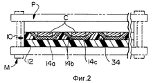
фиг. 1 - частичный аксонометрический вид самоцентрируемой проводящей схемы (SCN), изготовленной в соответствии с изобретением и соединенной с печатной схемой;
фиг. 2 - вид в разрезе в плоскости 2-2 фиг. 1;
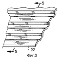
фиг. 3 и фиг. 4 - вид, подобный фиг. 1, показывающий последовательные стадии изготовления проводящей схемы, представленной на фиг. 1;
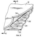
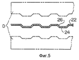
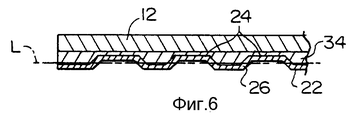
фиг. 5 и фиг. 6 - вид в разрезе в плоскости 5-5 и в плоскости 6-6 фиг. 3 и фиг. 4 соответственно;
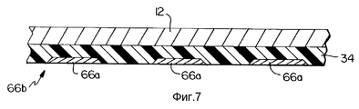
фиг. 7 - вид в разрезе части проводящей схемы, в которой удалены боковые стенки;
фиг. 8 - схематический вид, показывающий устройство для изготовления схем в соответствии с настоящим изобретением;
фиг. 9 - вид в разрезе, подобный показанному на фиг. 6, с изолированными проводниками и с прикрепленным упругим поддерживающим слоем для применения в соединительных узлах;
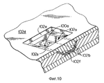
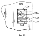
фиг. 10 и фиг. 11 - вид в перспективе и вид сверху соответственно, показывающие применение проводящей схемы для удержания припоя;
фиг. 12 и фиг. 13 - вид в разрезе, показывающий операцию плавления в холодном состоянии под давлением;
фиг. 14 и фиг. 15 представляют соответственно вид в разрезе элементов и собранной конструкции проводящей схемы в соответствии с настоящим изобретением, включая механически упрочненные контактные площадки и защиту;
фиг. 16-19 показывают способ изготовления проводящей схемы на подложке в соответствии с дополнительным примером исполнения изобретения.Now the invention will be described by way of example with reference to the attached drawings, in which:
FIG. 1 is a partial axonometric view of a self-centering conductive circuit (SCN) made in accordance with the invention and connected to a printed circuit;
FIG. 2 is a sectional view in the plane 2-2 of FIG. 1;
FIG. 3 and FIG. 4 is a view similar to FIG. 1, showing successive manufacturing steps of the conductive circuit shown in FIG. 1;
FIG. 5 and FIG. 6 is a sectional view in the plane 5-5 and in the plane 6-6 of FIG. 3 and FIG. 4 respectively;
FIG. 7 is a sectional view of a portion of a conductive circuit in which side walls are removed;
FIG. 8 is a schematic view showing an apparatus for manufacturing circuits in accordance with the present invention;
FIG. 9 is a sectional view similar to that shown in FIG. 6, with insulated conductors and with an attached elastic support layer for use in connecting nodes;
FIG. 10 and FIG. 11 is a perspective view and a top view, respectively, showing the use of a conductive circuit to hold solder;
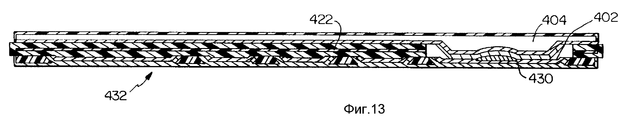
FIG. 12 and FIG. 13 is a sectional view showing the operation of melting in a cold state under pressure;
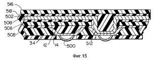
FIG. 14 and FIG. 15 are respectively a sectional view of the elements and the assembled structure of the conductive circuit in accordance with the present invention, including mechanically hardened pads and shields;
FIG. 16-19 show a method of manufacturing a conductive circuit on a substrate in accordance with a further exemplary embodiment of the invention.
Подробное описание конкретных исполнений изобретения. Detailed description of specific embodiments of the invention.
Рассмотрим фиг. 1 и фиг. 2, на которых показана гибкая проводящая схема в общем в позиции 10. Схема имеет диэлектрическую подложку 12, которая несет плотно упакованный блок самоцентрируемых проводящих путей 14. Показано, что проводящая схема 10 соединена с более или менее обычной проводящей схемой (например, печатная схема P), состоящей из подложки, которая несет ряд печатных проводящих путей или проводников C, расположенных так, что они взаимно сцепляются с проводящими путями 14 проводящей съемы 10. Обе показанные схемы соединены электрически и закреплены механически посредством зажима, показанного в позиции M на фиг. 2. Каждый проводящий путь 14 имеет нижнюю стенку 14a и пару разнесенных наклонных боковых стенок 14b, таким образом, сечение каждого проводящего пути 14 - в форме желобка. Нижняя стенка 14a обычно пропазована примерно от 0,025 мм (0,001 дюйма) до примерно 0,125 мм (0,005 дюйма) ниже поверхности проводящей схемы. Благодаря особому профилю или сечению проводящих путей 14 они взаимно пригоняются или сцепляются с соответствующими проводниками C схемы P для удержания проводников двух схем в правильном центрировании. Проводящая схема 10 лучше всего подходит для точного центрирования и поддержания контакта с проводниками, которые имеют расстояние меньше, чем примерно 3,8 мм (0,15 дюйма) и предпочтительно <0,6 мм (0,025 дюйма) по центру. Несмотря на их близкое расположение, смежные проводники не замыкаются. Consider FIG. 1 and FIG. 2, which shows a flexible conductive circuit generally in
Наклонные стороны 14b проводящих путей 14 направляют соответствующие проводники C в правильном центрировании с проводящей схемой 10, при этом образуются контактные соединения между проводниками двух схем. (Важно отметить, что проводящую схему можно применять на приемном или входящем контакте межсоединения). Желобчатые проводящие пути 14 также препятствуют разрыву проводников под действием вибрации, и они позволяют образовывать высокоплотные соединения между двумя проводящими схемами (например, 10 и P) внутри установленного рисунка. Следует отметить, что применение дополнительно клея (34) может улучшить соединение между двумя схемами. The inclined sides 14b of the
Хотя на фиг. 1 и фиг. 2 показано, что проводящие пути являются прямыми и расположены параллельно друг другу в плотно упакованной группе, однако проводящие пути могут иметь различный профиль и следовать по различному пути вдоль подложки 12 или взаимно соединяться в зависимости от конкретного применения схемы благодаря соответствующему контролю описанной операции формования. Although in FIG. 1 and FIG. 2 shows that the conductive paths are straight and parallel to each other in a tightly packed group, however, the conductive paths can have a different profile and follow a different path along the
Теперь рассмотрим фиг. 3 и фиг. 5, на которых показан способ изготовления в соответствии с одним примером исполнения изобретения гибкой проводящей схемы 10, заключающийся в том, что плоский металлический материал 22 (например, медный лист или фольга) соответствующей толщины, например, примерно 0,035 мм (0,0014 дюйма) очищают и точно подают между парой штампов, показанных в позиции D на фиг. 5, которые чеканят или осуществляют тиснение фольги 22 для образования неплоского рисунка, отличающегося рядом выступов 24 на одной стороне листа и соответствующим рядом желобков или каналов 26 на противоположной стороне листа. Обычно глубина каждого желобка составляет примерно от 0,038 мм (0,0015 дюйма) до примерно 0,013 мм (0,005 дюйма). Хотя на фиг. 3 и фиг. 5 показано, что выступы 24 имеют прямоугольное сечение или профиль, однако можно изготовить такие штампы D, чтобы выступы имели требуемую форму сечения (например, полусферическая, овальная, V-образная и т.п.). Процесс чеканки не только формует металлический лист 22, но также деформационно упрочняет его, подготавливает металлический лист к стадии наслоения, которая будет описана. Тонкие металлические листы могут потребовать конструкционной опоры для формующей матрицы во время наслаивания. Now consider FIG. 3 and FIG. 5, which shows a manufacturing method, in accordance with one embodiment of the invention, of a flexible
Как показано на фиг. 4 и фиг. 6, гибкий диэлектрический материал 12, например лист диэлектрика Kapton толщиной 0,025 мм (0,001 дюйма), можно наслоить на металлический лист 22 во время процесса формования. Наслаивание можно также осуществлять после формования. В показанном способе наслоения клейкий материал 34 наносят на одну сторону диэлектрического материала 12, и диэлектрический материал прижимают к стороне металлического листа 22, имеющей выступы 24, при этом в течение заданного отрезка времени прилагают тепло и давление, заставляя клейкий материал 34 течь и заполнять полости между выступами, как лучше всего показано на фиг. 6. Соответствующие материалы включают в себя, но без ограничения, эпоксидные клеи, полиэфиры и другие специальные клеи. As shown in FIG. 4 and FIG. 6, a flexible
Либо гибкий диэлектрический материал можно наплавить (например, через расплавление) на металлический лист и тем самым исключить необходимость в клее. Or, a flexible dielectric material can be fused (for example, by melting) onto a metal sheet and thereby eliminate the need for glue.
Затем слоистый материал, показанный на фиг. 6, подвергают прецизионному способу удаления металла, который механически удаляет заданное количество нежелательного металлического материала на стороне незащищенного металла в слоистом материале (например, материал, обозначенный ниже пунктирной линии L на фиг. 6), причем удаляют достаточное количество, чтобы образовать электрически изолированные проводящие пути. В результате способа прецизионного снятия металла образуется рисунок профилированных проводящих дорожек 14 проводящей схемы 10, показанной на фиг. 1 и фиг. 2. Затем проводящие дорожки можно очистить и нанести в них требуемое защитное покрытие (например, из золота, свинца или олова) для завершения изготовления проводящей схемы 10. Проводящие дорожки могут иметь расстояние, например, 0,3 мм (0,012 дюйма) по центру. Then, the laminate shown in FIG. 6 is subjected to a precision metal removal method that mechanically removes a predetermined amount of undesired metal material on the unprotected metal side of the laminate (for example, the material indicated below the dashed line L in FIG. 6), and a sufficient amount is removed to form electrically insulated conductive paths . As a result of the precision metal removal method, a pattern of profiled
Также, если заменить материалы подложки или основы, чтобы они были жесткими, а не гибкими, можно легко получить плату печатной схемы, имеющую канализированные или "плоские" проводники (как описано здесь), в соответствии с особенно предпочтительными исполнениями изобретения. В этом примере диэлектрическим материалом является жесткий диэлектрик. В других отношениях конструкция жесткой платы схемы соответствует конструкции показанной гибкой схемы. Таким образом, хотя описание, которое последует, в общем относится к гибким проводящим схемам, однако принципы изготовления схем можно использовать в равной степени для изготовления жестких плат схем. Also, by replacing the backing materials or substrates so that they are rigid and not flexible, it is easy to obtain a printed circuit board having channelized or “flat” conductors (as described here), in accordance with particularly preferred embodiments of the invention. In this example, the dielectric material is a rigid dielectric. In other respects, the design of the rigid circuit board corresponds to the design of the shown flexible circuit. Thus, although the description that follows generally refers to flexible conductive circuits, the principles of manufacturing circuits can be used equally for the manufacture of rigid circuit boards.
Проводящие пути и их терминальные точки можно образовать для любого конкретного электрического параметра (например, ток и сигнал) или любой конфигурации. Например, регулируемое полное сопротивление каждой проводящей дорожки можно выбрать такое, чтобы оно соответствовало конкретному применению, причем это достигается посредством соответствующего регулирования конфигурации дорожки и/или ее связи с электропроводящей несущей конструкцией (например, пружинный слой 58 или защита), если она есть. Важно отметить, что хотя на проводники и/или терминальные точки можно нанести любое защитное покрытие, если система проводников не соединена электрически с общей шиной гальванической ванны, однако, например, золото следует наносить, прежде чем проводящие дорожки будут электрически изолированы. Conducting paths and their terminal points can be formed for any specific electrical parameter (for example, current and signal) or any configuration. For example, the adjustable impedance of each conductive track can be selected to suit a particular application, and this is achieved by appropriately adjusting the configuration of the track and / or its connection with the electrically conductive supporting structure (e.g.,
Также в зависимости от применения проводящей схемы проводящие дорожки можно изолировать посредством нанесения верхнего слоя защитного покрытия или маски из припоя. Соответствующие изолирующие материалы включают в себя, но без ограничения Kapton, Mylar и Teflon. Это защитное покрытие обеспечивает средство для изготовления многослойных проводящих схем (например, многослойные платы схем) или для ввода защитного материала в проводящую схему. Also, depending on the application of the conductive circuit, the conductive paths can be insulated by applying an upper layer of a protective coating or a mask of solder. Suitable insulating materials include, but are not limited to, Kapton, Mylar, and Teflon. This protective coating provides a means for fabricating multilayer conductive circuits (e.g., multilayer circuit boards) or for introducing protective material into the conductive circuit.
В некоторых применениях канализированные проводники могут не потребоваться. Например, при изготовлении гибкой печатной схемы, требующей исключительной гибкости, боковая стенка, несмотря на то что она тонкая, действует так, что гибкость уменьшается. Следовательно, в этой конструкции канализированные проводники имеют недостаток. Таким образом, как показано на фиг. 7, способ удаления нежелательного металлического материала, например посредством однозубой фрезы с алмазными пластинами для прецизионного фрезерования, продолжают до тех пор, пока не будет достигнута требуемая толщина проводника 66a. Поэтому, как показано на фиг. 7, конфигурация проводника, не имеющая боковых стенок, в соответствии с другими примерами исполнения изобретения, но сохраняющая преимущества безопасного для окружающей среды нехимического способа изготовления и другие преимущества, позволяет получить конструкцию 66b, предлагающую значительное преимущество и низкую стоимость. In some applications, channeled conductors may not be required. For example, in the manufacture of a flexible printed circuit requiring exceptional flexibility, the side wall, although thin, acts so that flexibility is reduced. Therefore, in this design, the channeled conductors have a drawback. Thus, as shown in FIG. 7, the method for removing unwanted metal material, for example by means of a single-tooth cutter with diamond inserts for precision milling, is continued until the desired thickness of the
В отличие от некоторых известных способов изготовления проводящих схем (например, травление и осаждение) в способе в соответствии с этим изобретением не применяют реактив для травления, опасное для окружающей среды маскировочное покрытие, смывку и растворы для проявления. Таким образом, исключаются опасность для окружающей среды и затраты, связанные с транспортировкой отработанных растворов смывки, проявителя или маскировочного покрытия в места захоронения токсичных отходов. Также способ в соответствии с этим изобретением устраняет проблемы выхода изделий, связанные с обычными протравляемыми схемами, как, например, деформация оригинала фотошаблона или применение краски, имеющей плохую стойкость к кислоте, несоответствующее травление, вызванное присутствием пыли или грязи, или неэффективный способ травления. Итак, применение этого способа позволяет уменьшить затраты на изготовление и увеличить выход изделий. Unlike some known methods for the manufacture of conductive circuits (for example, etching and deposition) in the method in accordance with this invention do not use a reagent for etching, an environmentally harmful masking coating, rinsing and development solutions. In this way, environmental hazards and costs associated with transporting spent washing, developer or camouflage solutions to toxic waste disposal sites are eliminated. Also, the method in accordance with this invention eliminates product exit problems associated with conventional pickling patterns, such as deformation of the original photo mask or the use of a paint having poor acid resistance, inappropriate pickling caused by the presence of dust or dirt, or an ineffective pickling method. So, the application of this method allows to reduce manufacturing costs and increase the yield of products.
В сравнении с известными способами травления способ в соответствии с этим изобретением предлагает дополнительные преимущества. Для обеспечения равномерной скорости травления фольга, применяемая в способах травления, должна быть свободна от примесей. Однако в описанном способе можно применять медную фольгу с незначительными примесями. Кроме того, на процесс травления оказывает непосредственное влияние толщина фольги, поскольку линейная скорость прямо пропорциональна массе фольги (чем толще фольга, тем ниже линейная скорость). Compared to known etching methods, the method in accordance with this invention offers additional advantages. To ensure a uniform etching rate, the foil used in the etching methods must be free of impurities. However, in the described method, copper foil with minor impurities can be used. In addition, the thickness of the foil directly affects the etching process, since the linear velocity is directly proportional to the mass of the foil (the thicker the foil, the lower the linear velocity).
Способ, описанный со ссылкой на фиг. 1-7, допускает присутствие острых выпуклостей и мелких элементов. The method described with reference to FIG. 1-7, allows the presence of sharp bulges and small elements.
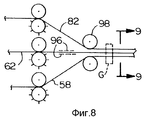
Способ шлифования, наслоения и чеканки, показанный на фиг. 8 и фиг. 9, аналогичен способу, применяемому для изготовления проводящей схемы, представленной на фиг. 1 и фиг. 2. В соответствии с этим способом лист 82 металлического материала, например медной фольги толщиной 0,035 мм (0,0014 дюйма), возможно со слоем золота, нанесенным под давлением, где оно требуется для электрических контактов, тянут с валка, очищают и подают точно между парой штампов D для чеканки или калибрующих валиков (не показаны), которые образуют рисунок из выступов и участков отходов, причем рисунок соответствует рисунку контактов или проводников 56. Полоски с нанесенным слоем золота образуют зоны контактов. Предпочтительно лист 82 снабжен ведущими отверстиями, которые точно совпадают со звездочками в механизме подачи (не показан), таким образом, полоса направляется точно в соответствующее место между штампами D. Этим способом чеканки выдавливаются нежелательные участки или отходы материала листа примерно на 0,05 мм (0,002 дюйма) - 0,125 мм (0,005 дюйма) выше поверхности выступов, определяющих проводники 56. Процесс чеканки, осуществляемый штампами D, также механически упрочняет "приподнятые" участки отходов фольги между выступами, следовательно, это позволяет упрочнить лист 82 и подготовить его к операции наслоения на линии, которая будет описана. The grinding, layering and embossing method shown in FIG. 8 and FIG. 9 is similar to the method used to fabricate the conductive circuit shown in FIG. 1 and FIG. 2. According to this method, a sheet of
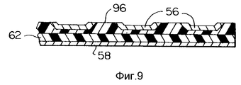
Как показано на фиг. 8 и фиг. 9, предварительно формованный металлический лист 82 затем точно центрируют с листом 58 пружинного металла (например, бериллиевая бронза), вытянутого с валка, таким образом, участки 86 отходов фольги обращены в сторону от листа 58. Между листами 58 и 82 подают лист 62 гибкого диэлектрического материала (например, 0,001-дюймовый полиэфир), который можно предварительно пробить (обработать методом окна) для открытия соединений заземления и/или наплавленных под давлением точек соединений. Если это требуется, то образованные под давлением межсоединения можно изготовить в виде двух проводящих листов, каждый из которых имеет противоположно расположенные механически упрочненные выпуклые части в точках соединения, проходящие между захватывающими роликами высокого давления. Это достигается, когда два листа проходящего материала размещают на каждой стороне предварительно пробитого гибкого диэлектрического материала. Противоположно расположенные, механически упрочненные выпуклые участки расплавляются под давлением, когда они проходят через захватывающие ролики высокого давления. Кроме того, каждое межсоединение структурно усиливается в процессе наслоения, как будет описано более подробно. Полученный таким образом слоистый пластик можно использовать в качестве упругой подложки в изготовлении соединителя, причем его можно также использовать для образования защиты и/или "земляного" слоя. As shown in FIG. 8 and FIG. 9, the
В этом показанном примере клеящий материал 96 наносят на обе поверхности листа 62, таким образом, когда три листа сжимаются вместе захватывающими роликами 98, они становятся наслоенными, образуя композиционный лист, состоящий из проводящего верхнего слоя 82, промежуточного диэлектрического слоя 62 и нижнего упругого слоя 58, при этом клеящий материал 96 заполняет полости под участками 86 отходов металла слоя 82. В других примерах исполнения слой 62 диэлектрика можно расплавить без деформации проводника, таким образом, можно исключить необходимость в клее между слоем 62 и проводящим верхним слоем 82. In this shown example,
В соответствии со следующей стадией способа слоистый материал подают через позицию полирования - шлифования или прецизионного фрезерования, обозначенную G на фиг. 8, на которой удаляют некоторое количество, например, 0,038 мм (0,0015 дюйма) приподнятых участков отходов листа 82, а также некоторое количество клеящего материала 96, таким образом, смежные выступы электрически изолируются и определяются окончательные формы тех выступов, которые теперь соответствуют рисункам проводящих путей 56. In accordance with a further step of the method, the laminate is fed through a polishing - grinding or precision milling position indicated by G in FIG. 8, in which a certain amount of, for example, 0.038 mm (0.0015 in.) Raised portions of the
Из описанного можно увидеть, что способ в соответствии с этим изобретением позволяет изготавливать гибкие проводящие схемы с узкими межсоединениями (например, схемы и перемычки) и обычные платы печатных схем высокого объема, причем относительно дешево. Можно следовать тем же принципам при изготовлении плотно упакованных блоков контактов для включения их в соединители, применяемые для соединения схем с узкими межсоединениями. From the described it can be seen that the method in accordance with this invention allows the manufacture of flexible conductive circuits with narrow interconnects (for example, circuits and jumpers) and conventional printed circuit boards of high volume, and relatively cheap. You can follow the same principles in the manufacture of tightly packed contact blocks to incorporate them into connectors used to connect circuits with narrow interconnects.
В конкретном исполнении для образования вывода проводника устройства часть пропазованных проводящих путей могут действовать в качестве приемников припоя, то есть они могут содержать некоторое количество припоя. После монтажа (и нагрева) приемник (приемники) припоя образует постоянное соединение с проводником (проводниками) устройства, при этом углубление в проводнике обеспечивает допуск для любой неплоскостности между устройством и проводником, который, будучи самоцентрируемым, упрощает размещение выводов проводников. Пропазованные проводники также позволяют уменьшить перемыкания припоя (между проводниками) и шариков припоя. In a particular embodiment, to form the lead of the device conductor, part of the pathogenized paths may act as solder receivers, that is, they may contain a certain amount of solder. After mounting (and heating), the solder receiver (s) forms a permanent connection with the device’s conductor (s), while the recess in the conductor provides tolerance for any non-flatness between the device and the conductor, which, being self-centered, simplifies the placement of the leads of the conductors. Displaced conductors can also reduce the solder shorting (between conductors) and solder balls.
Обратимся к фиг. 10 и фиг. 11, на которых показана типичная конфигурация (показан только один проводящий путь, хотя обычно применяют множество проводников), в которой припой 100a помещен в пропазованную полость 102a. Показанная пропазованная полость образована наклонными боковыми стенками 102b проводящего пути, боковой стенкой 102c (фиг. 11), оканчивающейся третьим выводом, и диэлектрическим изолирующим слоем 102d, либо диэлектрический слой 102d блокирует оба конца 102e полости (фиг. 10). В любой конфигурации прилагают затем тепло, при этом припой расплавляется на месте и вводят вывод устройства для электрического соединения с проводящим путем 102f. Если это требуется, то блокирующие элементы можно исключить. Turning to FIG. 10 and FIG. 11, which shows a typical configuration (only one conductive path is shown, although a plurality of conductors are usually used), in which the
Как показано на фиг. 12 и фиг. 13, согласно одному особенно предпочтительному исполнению межсоединения между двумя проводящими листами, полученного плавлением под давлением в соответствии с изобретением, диэлектрик 390, например 0,001-дюймовый Kapton с полиэфировым клеем на любой стороне, предварительно пробивают в позиции 400 для образования соединения между покрытой золотом медной фольгой 402 и проводящим материалом 404 защиты. В этом способе медную фольгу снабжают концентратором силы 410 в том месте, где должно образоваться наплавленное под давлением межсоединение. Концентратор силы механически упрочняют, и его можно снова заполнить клеем для дополнительного повышения его прочности и способности без разрушения. Предварительно перфорированный диэлектрик Kapton наслаивают на формованную медь, и в соответствии с описанным способом изготовления верхний слой медного пластика шлифуют. Концентратор силы 410 имеет высоту предпочтительно ниже уровня шлифования, таким образом, он не мешает процессу шлифования и его самого не подвергают шлифованию. As shown in FIG. 12 and FIG. 13, according to one particularly preferred embodiment of the interconnect between two conductive sheets obtained by pressure melting in accordance with the invention, a dielectric 390, for example a 0.001 inch Kapton with polyester adhesive on either side, is pre-punched at 400 to form a connection between the gold-plated
Полученную таким образом схему 414 проводников с концентратором силы (концентраторы) собирают с материалом 404 защиты, изготовленной, например, из медного листа 415, имеющего точку 416 межсоединения с покрытием и изолирующий слой 418, соединенный с материалом защиты через слой клея 420. Предварительно перфорированный слой 422 клея, обработанный методом окна или просверленный в позиции 424 для обнажения точки 416 межсоединения, размещают между материалом защиты и образованной схемой 414, и сборку наслаивают на месте. Во время процесса наслоения концентратор силы эффективно увеличивает значительную силу между точкой 416 металлизованного межсоединения защиты и проводником 402 образованной схемы 414 для получения наплавленного под давлением межсоединения в точке 430 для собранной схемы 432. Типичное давление, необходимое для этого межсоединения, составляет порядка 275 - 425 фунт/дюйм2. В соответствии с показанным примером исполнения проводник согласно изобретению можно соединить этим способом с элементом защиты, причем с достижением его преимущественных электрических свойств.The thus obtained
Теперь рассмотрим фиг. 14 и фиг. 15. На фиг. 14 показаны элементы схемы (проводящая схема на подложке - SCN) в соответствии с настоящим изобретением, включающей в себя механически упрочненную контактную площадку 500 и защиты 502. В этой конструкции проводящая схема 10 включает в себя контактные участки 504, покрытые золотом, которые образуют контактные зоны упрочненных концентраторов силы 500. Внутренняя полость этого концентратора состоит из меди, которая является частью пластины из медного листа, их которого образованы проводники. Слой 506 диэлектрического материала, например Kapton, для прикрепления к стороне проводника 14 проводящей схемы 10 имеет на своих обоих поверхностях клей 508, которым слой диэлектрического материала будет прикрепляться к стороне проводника 14 схемы 10 и к защите 502 для образования конструкции показанной в разрезе на фиг. 15. Диэлектрик 506 и его соответствующие слои 508 клея включают в себя отверстия или окна 510, позволяющие проходить присоединительному зажиму 512 защиты 502 для обеспечения контакта между металлическим кожухом 514 защиты 502 в контакте с частью проводящей схемы 14, чтобы его можно было пригонять с этой частью схемы за счет приложения давления. На средство защиты 502 наносят слой диэлектрического материала (Kapton) 516, который прикрепляют к материалу защиты слоем 518 клея. Этот клей также заполняет внутреннюю полость прижимного зажима 512. Now consider FIG. 14 and FIG. 15. In FIG. 14 shows circuit elements (SCN on a substrate — SCN) in accordance with the present invention, including a mechanically hardened
Механически упрочненные силовые концентраторы 500 можно применять для образования межсоединений путем сплавления под давлением, например, те, которые описаны со ссылкой на фиг. 12 и фиг. 13, для соединения конструкции, показанной на фиг. 15, с другими слоями проводников или с соединителями, платами печатных схем и т.п. Mechanically
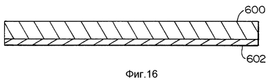
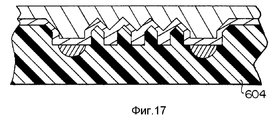
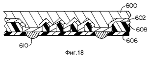
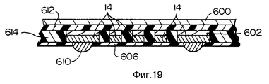
На фиг. 16-19 показан вариант исполнения изобретения, в котором применяют другой способ изготовления самой схемы. В этом варианте схему изготавливают из слоистого материала, состоящего из относительно толстого слоя 600 алюминия, на одну поверхность которого нанесли относительно тонкий слой 602 меди. В типичном примере такого слоистого материала слой алюминия может иметь толщину 0,25 мм (0,010 дюйма), а слой меди - примерно 0,025 мм (0,01 дюйма толщины). В зависимости от применения можно использовать другие материалы. Ими может быть золото или проводящая краска. Кроме того, на слой меди можно выборочно осадить золото для образования контактных участков. Слоистый материал 600, 602 формуют путем штамповки или прокатки с применением негативного шаблона 604, в который вводят с усилием слоистый материал, причем так, чтобы слой меди находился в контакте с негативным шаблоном 604. В результате, как показано на фиг. 18, образуется промежуточная структура, на медную сторону которой прикрепляют предварительно перфорированный слой диэлектрика (например, Kapton) 606 при помощи клея 608, который заполняет пространство между образованным слоем меди и слоем 606 диэлектрика. Силовые концентраторы 610, предназначенные для соединения с другими элементами схемы при помощи соответствующих средств, включая плавление под давлением, выступают через отверстия или окна, образованные в диэлектрике 606. In FIG. 16-19 show an embodiment of the invention in which another method of manufacturing the circuit itself is used. In this embodiment, the circuit is made of a layered material consisting of a relatively thick layer of
Затем незащищенный слой 600 и требуемые участки медного слоя 602 удаляют посредством соответствующей механической обработки, как было описано, для изоляции проводников 14, которые включают в себя участки 602 слоя меди, несомые усиливающими частями слоя 600 алюминия (фиг. 19), к которому прикрепляют слой диэлектрика (например, Kapton) 612 при помощи нанесения соответствующего клея 614. The exposed
В качестве варианта применения слоистого материала, описанного со ссылкой на фиг. 16-19, позитивный рисунок схемы можно получить из сплошного медного листа или другого соответствующего материала, затем слой диэлектрика можно прикрепить клеем к позитивному рисунку схемы и удалить отходы материала механическим способом, оставляя изолированные элементы 14 схемы. Это может быть достигнуто с применением силовых концентраторов или без них или как это требуется для конкретной конструкции. При применении этого способа образования рисунка проводников силовые концентраторы можно получить посредством выборочного уменьшения (шлифования) проводника до более низкого уровня, чем силовой концентратор. As an application of the laminate described with reference to FIG. 16-19, a positive pattern of the circuit can be obtained from a solid copper sheet or other appropriate material, then the dielectric layer can be glued to the positive pattern of the circuit with glue and remove the waste material mechanically, leaving the
В способе, описанном со ссылкой на фиг. 16-19 и в последующем описании с альтернативными материалами можно отметить, что слои алюминия 600 или толстый слой меди в основном предназначены для того, чтобы действовать в качестве гидравлической подушки и опоры для образования элементов схемы на поверхности слоя как одно целое и чтобы можно было точно разместить и удерживать эти элементы для таких последующих операций, как термообработка, наслоение, металлизация и т.п. In the method described with reference to FIG. 16-19 and in the following description with alternative materials, it can be noted that the aluminum layers 600 or a thick copper layer are mainly intended to act as a hydraulic cushion and support for forming circuit elements on the layer surface as a whole and so that it can be accurately place and hold these elements for such subsequent operations as heat treatment, layering, plating, etc.
Доказано, что это является наилучшим способом изготовления сложных деталей и/или элементов вдоль большой оси "Z", однако недостатком этого способа являются значительно большие отходы металла. It is proved that this is the best way to manufacture complex parts and / or elements along the major axis "Z", however, the disadvantage of this method is the significantly large waste metal.
В другом примере исполнения проводящую схему в соответствии с настоящим изобретением можно изготовить с использованием тонкого слоя меди или другого проводящего материала толщиной примерно 0,0125 см (0,0005 дюйма), поддерживаемым слоем термопластичного материала толщиной примерно 0,25 мм (0,010 дюйма). В этой конструкции медь становится схемой, тогда как термопласт действует в качестве гидравлической подушки и опорной конструкции во время обработки. Этот слоистый материал обрабатывают так же, как было описано для слоистого материала, содержащего алюминий и медь. Термопластичный материал можно прикрепить клеем к меди или нанести на слой меди литьем под давлением. In another embodiment, a conductive circuit in accordance with the present invention can be manufactured using a thin layer of copper or other conductive material with a thickness of about 0.0125 cm (0.0005 inches) supported by a layer of thermoplastic material with a thickness of about 0.25 mm (0.010 inches). In this design, copper becomes a circuit, while thermoplastic acts as a hydraulic cushion and supporting structure during processing. This laminate is treated in the same way as described for a laminate containing aluminum and copper. The thermoplastic material can be glued to copper or glued to a copper layer by injection molding.
В конструкциях, в которых диэлектрический материал прикрепляют клеем к меди, рисунок схемы можно образовать в слое меди с расположенным под ним слоем диэлектрика. Здесь клей вытесняется, образуя схемы и заполняя пустоты. In designs in which the dielectric material is glued to copper, the pattern can be formed in a copper layer with a dielectric layer located beneath it. Here the glue is squeezed out, forming patterns and filling voids.
В одной форме этого варианта исполнения слой меди или другого проводящего материала можно образовать на негативном шаблоне, изготовленном в форме для литья под давлением посредством приложения давления, создаваемого диэлектрическим материалом, вводимым в форму, для получения слоистого материала с проведением одновременно стадии формования. In one form of this embodiment, a layer of copper or other conductive material can be formed on a negative mold made in a mold for injection molding by applying pressure created by the dielectric material introduced into the mold to obtain a layered material while simultaneously conducting the molding step.
Как можно увидеть, способ в соответствии с настоящим изобретением является очень гибким, и он позволяет образовывать рисунок проводящей схемы согласно одному или нескольким, описанным здесь примерам исполнения, а также следующему дополнительному примеру, в котором проводящий материал наслаивают на диэлектрик и получают плоский слоистый пластик, которым может быть любой имеющийся в продаже пластик для изготовления проводящей схемы. Слоистый пластик может представлять собой лист диэлектрика, на который нанесли, напылили, металлизовали тонким проводящим материалом либо напечатали (штамповкой горячим формованием, формованием под давлением или под вакуумом) с применением шаблона, предназначенного для нагнетания или засасывания материала в верхний и нижний уровни, причем первый уровень расположен достаточно ниже верхнего уровня для исключения его повреждения во время удаления верхнего уровня. В этом варианте исполнения верхний и нижний уровни (построение контура или образование рельефа) образуют после изготовления слоистого материала. Обычно такой слоистый материал может содержать лист диэлектрического материала (например, Kapton) толщиной 0,0127 мм (0,0005 дюйма) со слоем меди толщиной 0,0063 мм (0,00025 дюйма), который просто формуют под вакуумом для образования слоистого пластика и рисунка проводящей схемы в неглубоком шаблоне. Шаблон позволяет изготавливать слоистый пластик со схемой проводников, расположенной достаточно ниже верхнего уровня для исключения повреждения схемы проводников, когда верхний уровень удаляют шлифованием, резанием или полированием. После удаления отходов слоистый материал можно прокатать до его плоского состояния для получения требуемой конфигурации схемы. Либо сопротивление деформации слоистого материала можно распределить таким образом, чтобы оно было недостаточным, чтобы вызвать постоянную деформацию, в результате которой слоистый материал во время последующего шлифования, резания или полирования будет деформироваться в шаблоне, после этого вакуум удаляют, и схема проводников возвращается к ее исходной плоской форме. Слоистые материалы для этой цели можно получить так же, как, например, группы проводников, формованных под вакуумом и наслоенных на лист диэлектрика с использованием слоя клея, либо проводников, деформированных и соединенных плавлением со слоем диэлектрика основы для исключения необходимости в клее. Это можно достичь, причем без деформации проводников, при применении способа в соответствии с настоящим изобретением. Этот способ может быть более дешевым, возможно, за счет ограниченного формования деталей, поскольку присутствующий диэлектрик действует в качестве "регулятора" формирования, которое может быть пределом. As you can see, the method in accordance with the present invention is very flexible, and it allows you to form a conductive circuit according to one or more of the examples described here, as well as the following additional example, in which the conductive material is layered on a dielectric and get a flat laminate, which can be any commercially available plastic for the manufacture of a conductive circuit. Laminate may be a dielectric sheet on which it is applied, sprayed, metallized with thin conductive material or printed (by hot forming, pressure molding or vacuum molding) using a template designed to inject or suck the material into the upper and lower levels, the first the level is located sufficiently below the upper level to prevent damage during removal of the upper level. In this embodiment, the upper and lower levels (building a contour or forming a relief) form after the manufacture of the layered material. Typically, such a laminate may comprise a sheet of dielectric material (e.g., Kapton) with a thickness of 0.0127 mm (0.0005 inches) with a copper layer with a thickness of 0.0063 mm (0.00025 inches), which is simply molded under vacuum to form a laminate and drawing a conductive circuit in a shallow pattern. The template allows you to make laminated plastic with a circuit of conductors located sufficiently below the upper level to prevent damage to the circuit of conductors when the upper level is removed by grinding, cutting or polishing. After the waste has been removed, the laminate can be rolled to its flat state to obtain the desired circuit configuration. Or, the deformation resistance of the layered material can be distributed so that it is insufficient to cause permanent deformation, as a result of which the layered material will deform in the template during subsequent grinding, cutting or polishing, then the vacuum is removed, and the conductor circuit returns to its original flat shape. Layered materials for this purpose can be obtained in the same way as, for example, groups of conductors molded under vacuum and layered on a dielectric sheet using an adhesive layer, or conductors deformed and fused with a base dielectric layer to eliminate the need for adhesive. This can be achieved, without deformation of the conductors, by applying the method in accordance with the present invention. This method may be cheaper, possibly due to the limited molding of the parts, since the dielectric present acts as a “regulator” of formation, which may be the limit.
Настоящее изобретение также позволяет изготавливать "скульптурные" (трехмерные) схемы, в которых некоторые участки схемы более толстые, чем другие участки, в результате образуются, например, жесткие контактные участки с гибкими межсоединениями. Это достигается за счет создания соответствующего трехмерного шаблона, который включает в себя требуемые характеристики (см. например, фиг. 16-19), с использованием проводящего материала или пластика из композиционного материала, который затем формуют, как описано со ссылкой на фиг. 16-19. The present invention also allows the manufacture of "sculptural" (three-dimensional) circuits in which some sections of the circuit are thicker than other sections, resulting in, for example, rigid contact sections with flexible interconnects. This is achieved by creating an appropriate three-dimensional template that includes the required characteristics (see, for example, FIGS. 16-19) using a conductive material or plastic made of composite material, which is then molded as described with reference to FIG. 16-19.
На схемы проводников и/или их терминальные точки можно нанести в соответствии с настоящим изобретением любое защитное покрытие, поскольку настоящее изобретение позволяет изготавливать схемы проводников из листового или рулонного проводящего материала, на который предварительно нанесли соответствующее контактное покрытие (например, золото). Такое решение возможно только со способом в соответствии с настоящим изобретением, поскольку каждый проводник образуют путем вышлифовывания нежелательного материала отходов между каждым проводником, таким образом, лишнее золото легко удаляется. Это противоположно известным системам травления, применяемым для изготовления плат печатных схем, поскольку обычные травильные растворы не будут удалять золото и, следовательно, потребуются дополнительные стадии обработки. Таким образом, настоящее изобретение значительно сокращает затраты на нанесение и выборочное удаление требуемого контактного покрытия. In accordance with the present invention, any protective coating can be applied to the circuitry of conductors and / or their terminal points, since the present invention makes it possible to produce circuitry of conductors from sheet or rolled conductive material, on which a corresponding contact coating has been previously applied (for example, gold). Such a solution is only possible with the method in accordance with the present invention, since each conductor is formed by grinding unwanted waste material between each conductor, so that excess gold is easily removed. This is the opposite of the known etching systems used to make printed circuit boards, since conventional etching solutions will not remove gold and therefore additional processing steps will be required. Thus, the present invention significantly reduces the cost of applying and selectively removing the desired contact coating.
Проводящую схему можно изолировать защитным покрытием, если это потребуется, и ее можно использовать для изготовления многослойных плат схем, размещенных одна на другой с соответствующим защитным промежуточным диэлектрическим материалом, изолирующим платы, за исключением тех мест, где требуется контакт через отверстия или окна. The conductive circuit can be insulated with a protective coating, if necessary, and it can be used for the manufacture of multilayer circuit boards placed on top of one another with the corresponding protective intermediate dielectric material insulating the boards, except for those places where contact through holes or windows is required.
Как было описано, межсоединения можно легко образовать путем плавления под давлением для соединения двух проводящих листов, один из которых имеет механически упрочненные выпуклости, расположенные в точках, где они должны взаимно соединяться с использованием роликов высокого давления. Это достигается с применением двух листов проводящей схемы, расположенных на каждой стороне предварительно пробитого слоя гибкого диэлектрика. Этим гибким диэлектрическим материалом толщиной, например, 0,025 мм (0,002 дюйма) может быть полиэфир. Механически упрочненные выпуклые участки образуют межсоединения путем плавления под давлением, когда они проходят через ролики высокого давления. Кроме того, каждое межсоединение структурно упрочняется в процессе наслоения. As described, the interconnects can be easily formed by melting under pressure to connect two conductive sheets, one of which has mechanically hardened bulges located at the points where they should be interconnected using high pressure rollers. This is achieved using two sheets of a conductive circuit located on each side of a pre-punched layer of flexible dielectric. This flexible dielectric material, for example 0.025 mm (0.002 in) thick, can be polyester. Mechanically hardened convex portions form interconnects by melting under pressure as they pass through high pressure rollers. In addition, each interconnect is structurally strengthened during the layering process.
Claims (28)
Applications Claiming Priority (3)
| Application Number | Priority Date | Filing Date | Title |
|---|---|---|---|
| US837357 | 1992-02-14 | ||
| US07837357 US5343616B1 (en) | 1992-02-14 | 1992-02-14 | Method of making high density self-aligning conductive networks and contact clusters |
| PCT/US1993/001454 WO1993016574A1 (en) | 1992-02-14 | 1993-02-10 | High density conductive networks and method and apparatus for making same |
Publications (2)
| Publication Number | Publication Date |
|---|---|
| RU94040379A RU94040379A (en) | 1996-08-10 |
| RU2138930C1 true RU2138930C1 (en) | 1999-09-27 |
Family
ID=25274222
Family Applications (1)
| Application Number | Title | Priority Date | Filing Date |
|---|---|---|---|
| RU94040379A RU2138930C1 (en) | 1992-02-14 | 1993-02-10 | Method for manufacturing of conducting circuit on substrate, conducting circuit on substrate and device for manufacturing of flexible conducting circuit |
Country Status (7)
| Country | Link |
|---|---|
| US (3) | US5343616B1 (en) |
| EP (1) | EP0626124A4 (en) |
| JP (1) | JPH07506218A (en) |
| KR (2) | KR950700676A (en) |
| CA (1) | CA2128210A1 (en) |
| RU (1) | RU2138930C1 (en) |
| WO (2) | WO1993016574A1 (en) |
Cited By (4)
| Publication number | Priority date | Publication date | Assignee | Title |
|---|---|---|---|---|
| RU2458491C1 (en) * | 2008-08-11 | 2012-08-10 | Шарп Кабусики Кайся | Flexible substrate and structure of electric circuit |
| RU2496286C1 (en) * | 2012-03-20 | 2013-10-20 | Федеральное государственное бюджетное образовательное учреждение высшего профессионального образования "Московский государственный технический университет имени Н.Э. Баумана (МГТУ им. Н.Э. Баумана) | Manufacturing method of flexible relief printed-circuit boards for electronic and electrotechnical equipment |
| RU2519942C2 (en) * | 2009-02-13 | 2014-06-20 | Сейдзи КАГАВА | Composite film of linearly scratched thin metal film and plastic film and apparatus for producing same |
| EA037451B1 (en) * | 2018-06-19 | 2021-03-30 | Федеральное государственное унитарное предприятие "Всероссийский научно-исследовательский институт автоматики им. Н.Л. Духова" | Method for making printed circuit boards |
Families Citing this family (53)
| Publication number | Priority date | Publication date | Assignee | Title |
|---|---|---|---|---|
| US5528001A (en) * | 1992-02-14 | 1996-06-18 | Research Organization For Circuit Knowledge | Circuit of electrically conductive paths on a dielectric with a grid of isolated conductive features that are electrically insulated from the paths |
| US5721007A (en) * | 1994-09-08 | 1998-02-24 | The Whitaker Corporation | Process for low density additive flexible circuits and harnesses |
| US5718789A (en) * | 1995-06-07 | 1998-02-17 | The Dexter Corporation | Method for making a debossed conductive film composite |
| US5928767A (en) * | 1995-06-07 | 1999-07-27 | Dexter Corporation | Conductive film composite |
| US6143989A (en) * | 1995-07-20 | 2000-11-07 | The Regents Of The University Of California | Active alignment/contact verification system |
| US5796158A (en) * | 1995-07-31 | 1998-08-18 | Micron Technology, Inc. | Lead frame coining for semiconductor devices |
| US5873739A (en) * | 1996-05-14 | 1999-02-23 | Miraco, Inc. | Direct circuit to circuit stored energy connector |
| US6085414A (en) * | 1996-08-15 | 2000-07-11 | Packard Hughes Interconnect Company | Method of making a flexible circuit with raised features protruding from two surfaces and products therefrom |
| US6182359B1 (en) * | 1997-01-31 | 2001-02-06 | Lear Automotive Dearborn, Inc. | Manufacturing process for printed circuits |
| US5995610A (en) * | 1997-05-06 | 1999-11-30 | Telefonaktiebolaget Lm Ericsson | Cooperative call processing across public and private intelligent networks |
| JP3282793B2 (en) * | 1997-12-02 | 2002-05-20 | 株式会社エンプラス | IC socket |
| US6299456B1 (en) * | 1998-04-10 | 2001-10-09 | Micron Technology, Inc. | Interposer with contact structures for electrical testing |
| US6140217A (en) * | 1998-07-16 | 2000-10-31 | International Business Machines Corporation | Technique for extending the limits of photolithography |
| US6359233B1 (en) * | 1999-10-26 | 2002-03-19 | Intel Corporation | Printed circuit board multipack structure having internal gold fingers and multipack and printed circuit board formed therefrom, and methods of manufacture thereof |
| DE10000090A1 (en) * | 2000-01-04 | 2001-08-30 | Elfo Ag Sachseln Sachseln | Electrical connecting element production method has embossed substrate provided with selectively etched conductive galvanic coating |
| JP2001326046A (en) * | 2000-05-17 | 2001-11-22 | Enplas Corp | Contact pin assembly |
| US6632343B1 (en) | 2000-08-30 | 2003-10-14 | Micron Technology, Inc. | Method and apparatus for electrolytic plating of surface metals |
| US6508674B1 (en) | 2000-10-18 | 2003-01-21 | Storage Technology Corporation | Multi-layer conductive device interconnection |
| US6641408B1 (en) | 2000-10-18 | 2003-11-04 | Storage Technology Corporation | Compliant contacts for conductive devices |
| US6699395B1 (en) | 2000-10-18 | 2004-03-02 | Storage Technology Corporation | Method of forming alignment features for conductive devices |
| US6431876B1 (en) | 2000-10-18 | 2002-08-13 | Storage Technology Corporation | Conductive trace interconnection |
| US6884313B2 (en) * | 2001-01-08 | 2005-04-26 | Fujitsu Limited | Method and system for joining and an ultra-high density interconnect |
| US6532654B2 (en) | 2001-01-12 | 2003-03-18 | International Business Machines Corporation | Method of forming an electrical connector |
| JP3924126B2 (en) * | 2001-01-16 | 2007-06-06 | アルプス電気株式会社 | Printed wiring board and manufacturing method thereof |
| EP1392391A4 (en) * | 2001-05-07 | 2009-12-09 | Cochlear Ltd | Process for manufacturing electrically conductive components |
| US6848944B2 (en) * | 2001-11-12 | 2005-02-01 | Fci Americas Technology, Inc. | Connector for high-speed communications |
| KR100841611B1 (en) * | 2001-11-27 | 2008-06-27 | 엘지디스플레이 주식회사 | An apparatus for fabricating plastic-liquid crystal display device |
| US6692816B2 (en) * | 2001-11-28 | 2004-02-17 | 3M Innovative Properties Company | Abrasion resistant electrode and device |
| US6826830B2 (en) * | 2002-02-05 | 2004-12-07 | International Business Machines Corporation | Multi-layered interconnect structure using liquid crystalline polymer dielectric |
| RU2222831C1 (en) * | 2002-05-18 | 2004-01-27 | Общество с ограниченной ответственностью "ВА Инструментс" | Warning optical device |
| FR2850493B1 (en) * | 2003-01-29 | 2005-10-21 | Alstom | METHOD FOR MANUFACTURING CONTACTING STRIPS FOR ELECTRICAL DEVICE CONNECTORS, AND CONTACTS STRIP FOR SUCH CONNECTORS |
| US7307502B2 (en) * | 2003-07-16 | 2007-12-11 | Marvell World Trade Ltd. | Power inductor with reduced DC current saturation |
| US7489219B2 (en) * | 2003-07-16 | 2009-02-10 | Marvell World Trade Ltd. | Power inductor with reduced DC current saturation |
| US7023313B2 (en) * | 2003-07-16 | 2006-04-04 | Marvell World Trade Ltd. | Power inductor with reduced DC current saturation |
| WO2005020215A1 (en) * | 2003-08-21 | 2005-03-03 | Sae Magnetics (H. K.) Ltd. | Electrical connection and component assembly for constitution of a hard disk drive |
| DE102004014435A1 (en) * | 2004-03-24 | 2005-11-17 | Siemens Ag | Arrangement with an integrated circuit |
| US8324872B2 (en) * | 2004-03-26 | 2012-12-04 | Marvell World Trade, Ltd. | Voltage regulator with coupled inductors having high coefficient of coupling |
| CN100442956C (en) * | 2005-03-25 | 2008-12-10 | 华通电脑股份有限公司 | Soft-hard composite circuit board manufacturing method |
| WO2007016688A1 (en) | 2005-08-02 | 2007-02-08 | New Way Machine Components, Inc. | A method and a device for depositing a film of material or otherwise processing or inspecting, a substrate as it passes through a vacuum environment guided by a plurality of opposing and balanced air bearing lands and sealed by differentially pumped groves and sealing lands in a non-contact manner |
| GB2436174B (en) * | 2006-03-15 | 2011-01-12 | Avago Technologies Fiber Ip | Connection arrangement and method for optical communications |
| KR100811768B1 (en) * | 2007-04-23 | 2008-03-07 | 삼성전기주식회사 | Manufacturing method of pcb |
| CN100574562C (en) * | 2007-07-06 | 2009-12-23 | 富葵精密组件(深圳)有限公司 | The manufacture method of hollowed-out PCB |
| CN101801155A (en) * | 2009-02-09 | 2010-08-11 | 富士康(昆山)电脑接插件有限公司 | Flexible printed circuit board and electric connector provided with same |
| EP2244291A1 (en) * | 2009-04-20 | 2010-10-27 | Nxp B.V. | Multilevel interconnection system |
| TWM365052U (en) * | 2009-05-15 | 2009-09-11 | Inventec Corp | Electromagnetic wave shielding device |
| US20110024160A1 (en) | 2009-07-31 | 2011-02-03 | Clifton Quan | Multi-layer microwave corrugated printed circuit board and method |
| US9072164B2 (en) * | 2009-11-17 | 2015-06-30 | Raytheon Company | Process for fabricating a three dimensional molded feed structure |
| RU2497320C1 (en) * | 2012-02-13 | 2013-10-27 | Общество с ограниченной ответственностью "Тегас Электрик" | Composite printed-circuit board |
| RU2529742C1 (en) * | 2013-02-22 | 2014-09-27 | Общество с ограниченной ответственностью "Тегас Электрик" | Method for manufacturing of composite printed circuit board |
| JP6599853B2 (en) * | 2013-06-21 | 2019-10-30 | サンミナ コーポレーション | Method of forming a laminated structure having plated through holes using a removable cover layer |
| CN104254190B (en) * | 2013-06-26 | 2017-12-01 | 陈丽专 | The preparation method of circuit board |
| RU2604721C1 (en) * | 2015-06-24 | 2016-12-10 | Российская Федерация, от имени которой выступает Государственная корпорация по атомной энергии "Росатом" (Госкорпорация "Росатом") | Manufacturing method of textured printed-circuit board |
| TWI726427B (en) * | 2019-09-27 | 2021-05-01 | 友達光電股份有限公司 | Device substrate |
Family Cites Families (51)
| Publication number | Priority date | Publication date | Assignee | Title |
|---|---|---|---|---|
| US2427144A (en) * | 1936-11-23 | 1947-09-09 | Jansen Franciscus Jo Wilhelmus | Mechanical connection for electrical circuits |
| US2638660A (en) * | 1945-04-03 | 1953-05-19 | Philips Lab Inc | Electrical insulator |
| US2716268A (en) * | 1952-10-16 | 1955-08-30 | Erie Resistor Corp | Method of making printed circuits |
| US2757443A (en) * | 1953-01-21 | 1956-08-07 | Erie Resistor Corp | Method of making printed circuits |
| US2837619A (en) * | 1954-08-30 | 1958-06-03 | Stein Samuel | Strain sensitive element and method of manufacture |
| US2912745A (en) * | 1955-08-25 | 1959-11-17 | Erie Resistor Corp | Method of making a printed circuit |
| US2912746A (en) * | 1955-10-10 | 1959-11-17 | Erie Resistor Corp | Method of making printed circuit panels |
| US2912748A (en) * | 1956-05-28 | 1959-11-17 | Erie Resistor Corp | Method of making printed circuit panels |
| US3148098A (en) * | 1960-11-03 | 1964-09-08 | Day Company | Method of producing electrical components |
| GB993885A (en) * | 1961-03-03 | 1965-06-02 | Aktiebolaget Electrolux | |
| US3301730A (en) * | 1961-04-03 | 1967-01-31 | Rogers Corp | Method of making a printed circuit |
| BE630656A (en) * | 1961-10-23 | |||
| US3158421A (en) * | 1961-12-04 | 1964-11-24 | Gen Dynamics Corp | Electrical connector for a printed circuit board and cable |
| US3147054A (en) * | 1962-06-14 | 1964-09-01 | Rca Corp | Test point extender for circuit boards |
| GB1126370A (en) * | 1965-12-29 | 1968-09-05 | British Aircraft Corp Ltd | Improvements relating to printed circuits |
| AU5650665A (en) * | 1966-01-25 | 1967-07-27 | Telephone & Electrical Industries Pty. Ltd | Printed circuits |
| US3423260A (en) * | 1966-03-21 | 1969-01-21 | Bunker Ramo | Method of making a thin film circuit having a resistor-conductor pattern |
| US3434208A (en) * | 1966-12-16 | 1969-03-25 | William H Toomey | Circuit assembly process |
| US3488890A (en) * | 1967-03-09 | 1970-01-13 | Western Electric Co | Method of and apparatus for adjusting film resistors to a desired resistance value |
| DE1665944A1 (en) * | 1967-05-13 | 1971-04-08 | Siemens Ag | Process for making electrical circuits |
| US3612745A (en) * | 1970-07-08 | 1971-10-12 | Sierracin Corp | Flexural bus bar assembly |
| US3875542A (en) * | 1971-02-10 | 1975-04-01 | Tektronix Inc | High frequency fuse |
| US3889363A (en) * | 1971-02-16 | 1975-06-17 | Richard P Davis | Method of making printed circuit boards |
| CA963237A (en) * | 1971-05-14 | 1975-02-25 | Frank L. Dieterich | Method and blank for making potentiometer contact springs |
| DE2136386A1 (en) * | 1971-07-21 | 1973-02-01 | Wagner Schaltungstechnik | ELECTRICAL FUSE AND METHOD OF MANUFACTURING IT |
| DE2305883A1 (en) * | 1973-02-07 | 1974-08-15 | Finsterhoelzl Rafi Elekt | CIRCUIT BOARD |
| US4089734A (en) * | 1974-09-16 | 1978-05-16 | Raytheon Company | Integrated circuit fusing technique |
| US4075420A (en) * | 1975-08-28 | 1978-02-21 | Burroughs Corporation | Cover layer for flexible circuits |
| US4357750A (en) * | 1976-06-21 | 1982-11-09 | Advanced Circuit Technology Inc. | Jumper cable |
| US4080027A (en) * | 1976-07-30 | 1978-03-21 | Gte Sylvania Incorporated | Electrical contact and connector |
| US4020548A (en) * | 1976-08-25 | 1977-05-03 | Western Electric Company, Inc. | Forming and stripping of conductors |
| US4091125A (en) * | 1976-11-08 | 1978-05-23 | Delgadillo Joseph A | Circuit board and method for producing same |
| US4306925A (en) * | 1977-01-11 | 1981-12-22 | Pactel Corporation | Method of manufacturing high density printed circuit |
| CH642772A5 (en) * | 1977-05-28 | 1984-04-30 | Knudsen Ak L | ELECTRICAL MELTFUSE AND THEIR PRODUCTION METHOD. |
| US4272753A (en) * | 1978-08-16 | 1981-06-09 | Harris Corporation | Integrated circuit fuse |
| US4406062A (en) * | 1979-11-05 | 1983-09-27 | Thomas & Betts Corporation | Method of forming a multichannel connector |
| US4532152A (en) * | 1982-03-05 | 1985-07-30 | Elarde Vito D | Fabrication of a printed circuit board with metal-filled channels |
| US4604799A (en) * | 1982-09-03 | 1986-08-12 | John Fluke Mfg. Co., Inc. | Method of making molded circuit board |
| US4775611A (en) * | 1983-11-10 | 1988-10-04 | Sullivan Donald F | Additive printed circuit boards with flat surface and indented primary wiring conductors |
| US4528259A (en) * | 1983-11-10 | 1985-07-09 | Sullivan Donald F | Printed wiring boards with solder mask over bare copper wires having large area thickened circuit pad connections |
| US4501638A (en) * | 1983-12-05 | 1985-02-26 | E. I. Du Pont De Nemours And Company | Liquid chemical process for forming conductive through-holes through a dielectric layer |
| US4655518A (en) * | 1984-08-17 | 1987-04-07 | Teradyne, Inc. | Backplane connector |
| US4651417A (en) * | 1984-10-23 | 1987-03-24 | New West Technology Corporation | Method for forming printed circuit board |
| US4721550A (en) * | 1986-05-05 | 1988-01-26 | New West Technology Corporation | Process for producing printed circuit board having improved adhesion |
| US4806106A (en) * | 1987-04-09 | 1989-02-21 | Hewlett-Packard Company | Interconnect lead frame for thermal ink jet printhead and methods of manufacture |
| US4840702A (en) * | 1987-12-29 | 1989-06-20 | Action Technologies, Inc. | Apparatus and method for plasma treating of circuit boards |
| US4912844A (en) * | 1988-08-10 | 1990-04-03 | Dimensional Circuits Corporation | Methods of producing printed circuit boards |
| US4996391A (en) * | 1988-09-30 | 1991-02-26 | Siemens Aktiengesellschaft | Printed circuit board having an injection molded substrate |
| CH680483A5 (en) * | 1989-10-20 | 1992-08-31 | Kobe Properties Ltd | |
| JP2806580B2 (en) * | 1989-12-15 | 1998-09-30 | 日本電気株式会社 | Surface mount connector |
| US5097101A (en) * | 1991-02-05 | 1992-03-17 | Tektronix, Inc. | Method of forming a conductive contact bump on a flexible substrate and a flexible substrate |
-
1992
- 1992-02-14 US US07837357 patent/US5343616B1/en not_active Expired - Fee Related
-
1993
- 1993-02-10 EP EP93906970A patent/EP0626124A4/en not_active Withdrawn
- 1993-02-10 WO PCT/US1993/001454 patent/WO1993016574A1/en not_active Application Discontinuation
- 1993-02-10 KR KR1019940702819A patent/KR950700676A/en not_active IP Right Cessation
- 1993-02-10 JP JP5514353A patent/JPH07506218A/en active Pending
- 1993-02-10 WO PCT/US1993/001484 patent/WO1993016575A1/en active Application Filing
- 1993-02-10 US US08/016,002 patent/US5477612A/en not_active Expired - Fee Related
- 1993-02-10 CA CA002128210A patent/CA2128210A1/en not_active Abandoned
- 1993-02-10 RU RU94040379A patent/RU2138930C1/en active
-
1994
- 1994-05-18 US US08/245,707 patent/US5526565A/en not_active Expired - Fee Related
- 1994-08-12 KR KR940702819A patent/KR100298010B1/ko active
Cited By (5)
| Publication number | Priority date | Publication date | Assignee | Title |
|---|---|---|---|---|
| RU2458491C1 (en) * | 2008-08-11 | 2012-08-10 | Шарп Кабусики Кайся | Flexible substrate and structure of electric circuit |
| US8754332B2 (en) | 2008-08-11 | 2014-06-17 | Sharp Kabushiki Kaisha | Display device |
| RU2519942C2 (en) * | 2009-02-13 | 2014-06-20 | Сейдзи КАГАВА | Composite film of linearly scratched thin metal film and plastic film and apparatus for producing same |
| RU2496286C1 (en) * | 2012-03-20 | 2013-10-20 | Федеральное государственное бюджетное образовательное учреждение высшего профессионального образования "Московский государственный технический университет имени Н.Э. Баумана (МГТУ им. Н.Э. Баумана) | Manufacturing method of flexible relief printed-circuit boards for electronic and electrotechnical equipment |
| EA037451B1 (en) * | 2018-06-19 | 2021-03-30 | Федеральное государственное унитарное предприятие "Всероссийский научно-исследовательский институт автоматики им. Н.Л. Духова" | Method for making printed circuit boards |
Also Published As
| Publication number | Publication date |
|---|---|
| CA2128210A1 (en) | 1993-08-19 |
| WO1993016575A1 (en) | 1993-08-19 |
| KR100298010B1 (en) | 2001-11-22 |
| US5526565A (en) | 1996-06-18 |
| RU94040379A (en) | 1996-08-10 |
| KR950700676A (en) | 1995-01-16 |
| US5343616B1 (en) | 1998-12-29 |
| WO1993016574A1 (en) | 1993-08-19 |
| EP0626124A1 (en) | 1994-11-30 |
| EP0626124A4 (en) | 1995-11-15 |
| US5343616A (en) | 1994-09-06 |
| JPH07506218A (en) | 1995-07-06 |
| US5477612A (en) | 1995-12-26 |
Similar Documents
| Publication | Publication Date | Title |
|---|---|---|
| RU2138930C1 (en) | Method for manufacturing of conducting circuit on substrate, conducting circuit on substrate and device for manufacturing of flexible conducting circuit | |
| EP0806127B1 (en) | An environmentally desirable printed circuit and associated apparatus | |
| US5584120A (en) | Method of manufacturing printed circuits | |
| US5334279A (en) | Method and apparatus for making printed circuit boards | |
| US7229293B2 (en) | Connecting structure of circuit board and method for manufacturing the same | |
| US4985601A (en) | Circuit boards with recessed traces | |
| EP0545328B1 (en) | Printed circuit board manufacturing process | |
| EP0843955B1 (en) | Method of forming raised metallic contacts on electrical circuits | |
| US5738797A (en) | Three-dimensional multi-layer circuit structure and method for forming the same | |
| KR100307671B1 (en) | Wiring structure, manufacturing method thereof, and circuit board using the wiring structure | |
| CA2109687A1 (en) | Method for the through plating of conductor foils | |
| US6243946B1 (en) | Method of forming an interlayer connection structure | |
| WO1993024939A1 (en) | Laminated conductive material, multiple conductor cables and methods of manufacturing such cables | |
| US6477052B1 (en) | Multiple layer thin flexible circuit board | |
| EP0147566B1 (en) | Method of forming contacts for flexible module carriers | |
| JP2001177224A (en) | Microwave circuit substrate and manufacturing method | |
| US4992059A (en) | Ultra fine line cable and a method for fabricating the same | |
| US4889962A (en) | Circuit board with coaxial circuit and method therefor | |
| WO2001065595A2 (en) | A method of forming an opening or cavity in a substrate for receiving an electronic component | |
| JPH06120623A (en) | Wiring board | |
| CN117855185A (en) | LGA substrate with side bonding pads and manufacturing process thereof | |
| JPH0634436B2 (en) | Printed wiring board for IC card | |
| JPH11346039A (en) | Flexible printed wiring board and its manufacture | |
| JPS614295A (en) | Method of producing printed circuit board | |
| JPH0846322A (en) | Manufacture of printed wiring board |