KR920004340B1 - Power source switching circuit - Google Patents
Power source switching circuit Download PDFInfo
- Publication number
- KR920004340B1 KR920004340B1 KR1019890008314A KR890008314A KR920004340B1 KR 920004340 B1 KR920004340 B1 KR 920004340B1 KR 1019890008314 A KR1019890008314 A KR 1019890008314A KR 890008314 A KR890008314 A KR 890008314A KR 920004340 B1 KR920004340 B1 KR 920004340B1
- Authority
- KR
- South Korea
- Prior art keywords
- mos transistor
- level
- potential
- transistor
- mos transistors
- Prior art date
Links
Images


Classifications
-
- H—ELECTRICITY
- H03—ELECTRONIC CIRCUITRY
- H03K—PULSE TECHNIQUE
- H03K17/00—Electronic switching or gating, i.e. not by contact-making and –breaking
- H03K17/51—Electronic switching or gating, i.e. not by contact-making and –breaking characterised by the components used
- H03K17/56—Electronic switching or gating, i.e. not by contact-making and –breaking characterised by the components used by the use, as active elements, of semiconductor devices
-
- H—ELECTRICITY
- H03—ELECTRONIC CIRCUITRY
- H03K—PULSE TECHNIQUE
- H03K17/00—Electronic switching or gating, i.e. not by contact-making and –breaking
- H03K17/10—Modifications for increasing the maximum permissible switched voltage
- H03K17/102—Modifications for increasing the maximum permissible switched voltage in field-effect transistor switches
-
- H—ELECTRICITY
- H03—ELECTRONIC CIRCUITRY
- H03K—PULSE TECHNIQUE
- H03K17/00—Electronic switching or gating, i.e. not by contact-making and –breaking
- H03K17/51—Electronic switching or gating, i.e. not by contact-making and –breaking characterised by the components used
- H03K17/56—Electronic switching or gating, i.e. not by contact-making and –breaking characterised by the components used by the use, as active elements, of semiconductor devices
- H03K17/687—Electronic switching or gating, i.e. not by contact-making and –breaking characterised by the components used by the use, as active elements, of semiconductor devices the devices being field-effect transistors
- H03K17/693—Switching arrangements with several input- or output-terminals, e.g. multiplexers, distributors
Abstract
내용 없음.No content.
Description
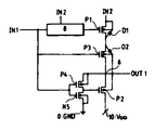
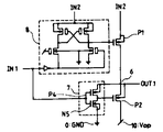
제 1 도는 본 발명에 따른 전원절환회로의 1실시예를 나타낸 회로구성도,1 is a circuit diagram showing an embodiment of a power supply switching circuit according to the present invention;
제 2 도는 제 1 도에 도시된 본 발명의 실시예를 설명하기 위한 도면,2 is a view for explaining an embodiment of the present invention shown in FIG.
제 3 도는 본 발명에 따른 전원절환회로의 변형예를 나타낸 회로도,3 is a circuit diagram showing a modification of the power supply switching circuit according to the present invention,
제 4 도는 종래의 전원절환회로의 일예를 나타낸 회로도,4 is a circuit diagram showing an example of a conventional power supply switching circuit;
제 5 도는 제 4 도에 도시된 회로의 결점을 설명하기 위한 도면이다.5 is a view for explaining the shortcomings of the circuit shown in FIG.
* 도면의 주요부분에 대한 부호의 설명* Explanation of symbols for main parts of the drawings
P1 : 제 1p챈널형 MOS트랜지스터 P2 : 제 2p챈널형 MOS 트랜지스터P1: 1p channel type MOS transistor P2: 2p channel type MOS transistor
P3 : 제 3p챈널형 MOS트랜지스터 P4 : p챈널형 MOS트랜지스터P3: 3p channel type MOS transistor P4: p channel type MOS transistor
N5 : n챈널형 MOS트랜지스터 6 : 접속점N5: n-channel MOS transistor 6: Connection point
7 : 인버터 8 : 레벨시프터7 Inverter 8 Level Shifter
10 : 기준전위단자10: reference potential terminal
[산업상의 이용분야][Industrial use]
본 발명은 CMOS에 관한 것으로, 특히 출력단자에서의 출력전위레벨을 학실하게 유지시킬 수 있으면서, 입력단자를 다른 입력신호에 대해 공용할 수 있도록 된 전원절환회로에 관한 것이다.BACKGROUND OF THE
[종래의 기술 및 그 문제점][Traditional Technology and Problems]
EPROM등을 사용하는 대규모집적회로(LST)에서는 기록 모우드시 전원전위("VDD)보다 높은 전위를 기록용전위로서 인가할 필요가 있는 바, 이 경우에는 기준전위와 그 기준전위보다 높은 전위를 전원으로 사용하여 절환해주어야만 된다.In a large-scale integrated circuit (LST) using an EPROM or the like, a potential higher than the power supply potential ("V DD ) needs to be applied as a recording potential in the recording mode. In this case, the reference potential and the potential higher than the reference potential are applied. It should be used as a power source for switching.
종래, 상기와 같이 전원을 절환하는 회로로서는 여컨대 제 4 도에 도시된 전원절환회로가 소개되어 있는데, 이 제 4 도에 도시된 종래의 전원절환회로에서는 직렬로 제 제 1p챈널형 MOS트랜지스터(P1)와 제 2p챈널형 MOS 트랜지스터(P2)가 갖추어져 있으면서, 이 제 1p챈널형 MOS트랜지스터(P1)의 소오스에는 입력단자(1N2)로부터 고전위 "VPP"레벨이 공급된느 반면, 제 2p챈널형 MOS 트랜지스터(P2)의 드레인에는 기준전위 단자(10)로부터 "VDD"레벨이 공급되게 된다.Conventionally, as the circuit for switching the power as described above, for example, the power switching circuit shown in FIG. 4 is introduced. In the conventional power switching circuit shown in FIG. 4, the first p-channel MOS transistor ( P1) and the second p-channel MOS transistor P2 are provided, and the source of the first p-channel MOS transistor P1 is supplied with the high potential "V PP " level from the input terminal 1N2, while the second p is provided. The "V DD " level is supplied from the reference
또한, 제 어신호가 입력되는 입력단자(IN1)에는 레벨시프터(8)의 입력이 접속되는 한편, 이 레벨시프터(8)를 매개해서 제 1p챈널형 MOS트랜지스터(P1)의 게이트가 접속되고, 또 입력단자(IN1)에는 p챈널형 MOS 트랜지스터(P4) 및 n챈널형 MOS 트랜지스터(N5)로 구성된 인버터회로(7)의 게이트가 접속된다. 그리고, 출력단자(OUT1)에는 상기 제 1p챈널형 MOS트랜지스터(P1)의 드레인과 제 2p챈널형 MOS트랜지스터(P2)의 소오스가 접속된 접속점이 연결됨과 더불어, p챈널형 MOS 트랜지스터(P4) 및 n챈널형 MOS 트랜지스터(N5)를 매개해서 접지단자의 "GND"레벨이 접속되며, 상기 제 2p챈널형 MOS 트랜지스터(P2)의 게이트에는 p챈널형 MOS 트랜지스터(P4)와 n챈널형 MOS 트랜지스터(N5)의 접속점이 접속되어 있다.In addition, the input of the level shifter 8 is connected to the input terminal IN1 to which the control signal is input, while the gate of the first p-channel MOS transistor P1 is connected via the level shifter 8. The input terminal IN1 is connected with a gate of an
이어, 이러한 종래예의 전원절환회로의 동작에 대해 설명하면 다음과 같다.Next, the operation of the power switching circuit of the conventional example will be described.
입력단자(IN2)에는 "VDD"레벨보다 높은 전위인 "VPP"레벨인 입력신호가 인가되는 바, 여기서 상기 레벨 시프터(8)는 입력단자(IN1) "VDD"레벨이 입력되는 경우 제 1p챈널형 MOS 트랜지스터(P1)를 완전히 OFF 시키기 위해 설치되는 것으로, 입력단자 (IN1)에 "GND"레벨이 입력되는 경우 "GND"레벨을 출력하는 회로이다.An input signal having a "V PP " level, which is a potential higher than the "V DD " level, is applied to the input terminal IN2, where the level shifter 8 is input to the input terminal IN1 "V DD " level. The circuit is provided to completely turn off the first p-channel MOS transistor P1, and outputs the "GND" level when the "GND" level is input to the input terminal IN1.
이 제 4 도에 도시된 회로구성에서, 먼저 입력단자(IN1) "GND"레벨이 입력되면서 입력단자(IN2)에 "VPP"레벨이 입력되게 되면, 제 1p챈널형 MOS 트랜지스터(P1)의 게이트에는 레벨시프터(8)의 출력인 "GND"레벨이 인가되어 제 1p챈널형 MOS 트랜지스터(P1)가 ON되고, 이에 따라 제 1p챈널형 MOS 트랜지스터 (P2)의 소오스가 접속된 접속점(6)은 "VPP"레벨로 된다. 또한, 입력단자(IN1)에 접속된 인버터(7)의 n챈널형 MOS트랜지스터 (N5)의 게이트에 "GND"레벨이 인가되므로 n챈널형 MOS트랜지스터(N5)가 OFF 된다. 이에 대해 입력단자(IN1)에 접속된 p챈널형 MOS 트랜지스터(P4)의 게이트에도 "GND"레벨이 인가되는데, 이 경우 접속점(6)이 "VPP"레벨이므로 p챈널형 MOS 트랜지스터(P4)는 ON되고, 이 p챈널형 MOS 트랜지스터(P4)를 매개해서 제 2p챈널형 MOS 트랜지스터(P2)의 게이트가 "VPP"레벨로 되어 제 2p 챈널형 MOS 트랜지스터(P2)는 완전히 OFF되므로 출력단자(OUT1)로부터 "VPP"레벨의 전위가 출력되게 된다.In the circuit configuration shown in FIG. 4, when the "GPP" level is input to the input terminal IN2 and the "V PP " level is input to the input terminal IN2, the first P-channel MOS transistor P1 is connected. A "GND" level, which is the output of the level shifter 8, is applied to the gate to turn on the first p-channel MOS transistor P1, whereby the
그리고, 입력단자(IN1) "VDD"레벨이 입력되게 되면, 제 1p챈널형 MOS트랜지스터(P1)의 게이트이는 레벨시프터(8)의 출력인"VPP"레벨이 인가되어 상기 제 1p챈널형 MOS트랜지스터(P1)는 완전히 OFF되고, 입력단자(IN1) 에 접속된 인버터(7)의 n챈널형 MOS트랜지스터 (N5)의 게이트에는 "VDD"레벨 인가되므로 그 n챈널형 MOS트랜지스터 (N5)가 ON이 되며, 제 2p챈널형MOS 트랜지스터(P2)의 게이트는 "GND "레벨로 되어 제 2p탠널형MOS 트랜지스터(P2)는 ON 된다. 따라서, 제 1p챈널형 MO S트랜지스터(P1)의 드레인과 제 2p탠널형MOS 트랜지스터(P2)의 소오스가 접속된 접속점(6)은 "VDD"레벨이기 때문에 이 p챈널형MOS 트랜지스터(P4)의 게이트 및 소오스가 모두"VDD"레벨이기 때문에 이 p챈널형MOS 트랜지스터(P4)가 OFF가 됨에 따라 접속점(6)의 "VDD"레벨이 그대로 출력단자(OUT1)로부터 출력되게 된다.When the input terminal IN1 "V DD " level is input, the gate of the first p-channel MOS transistor P1 is applied to the "V PP " level, which is the output of the level shifter 8, and thus the first p-channel type. Since the MOS transistor P1 is completely turned off and the gate of the n-channel MOS transistor N5 of the
상기한 바와같이 제 4 도에 도시된 종래예의 전원절환회로에서 입력단자(IN1)에 " GND"레벨이 입력되면 출력단자(OUT1)로부터 "VPP"레벨이 출력되는 반면, 입력단자(INI)에 "VDD"레벨이 입력되면 출력단자(OUT1)로부터 "VDD"레벨이 출력되게 된다.As described above, when the "GND" level is input to the input terminal IN1 in the power switching circuit of the conventional example shown in FIG. 4, the "V PP " level is output from the output terminal OUT1, whereas the input terminal INI is presented in "V DD" level is input when the "V DD" level is output from an output terminal (OUT1).
한편, 고전위 입력단자(IN2)에 인가되는 전위가 "VDD"레벨과 동등한 전위이거나 그 보다 높은 레벨인 경우에는 제 5 도에 도시된 바와같이 제 1p챈널형 MOS트랜지스터(P1) 의 소오스확산영역(P형)과 N웰(N Well) 사이에 존재하는 기생다이오드(D1)에 순방향바이어스가 가해지지 않게 되므로 전류가 흐르지 않게 되지만, 입력단자(IN 2)에 인가되는 전위가 "VDD"레벨보다 낮은 경우에는 제 1p챈널형 MOS트랜지스터(P1)가 OFF되어 있음에도 불구하고, 기생다이오드(D1)에는 순방향바이어스가 가해지게 되어 도통되므로 제 1 및 제 2p챈널형 MOS 트랜지스터(P1, P2) 매개하는 VDD단자(10)와 입력단자(IN2)사이에 전류경로가 형성되어 출력단자(OUT1)로부터 출력레벨이 저하되게 된다. 이와같이 종래의 전위절환로에서는 입력단자(IN2)로부터 인가되는 전위가 "VDD"레벨보다 낮은 경우에는 상기와 같은 결점이 있기 때문에 고전위 입력신호에 대해서는 다른 입력단자(IN2)를 겸용할 수가 없게 되므로 각 입력신호에 대해 각각의 전용단자를 설치해주어야 한다는 결점이 있었다.On the other hand, when the potential applied to the high potential input terminal IN2 is equal to or higher than the "V DD " level, the source diffusion of the first p-channel MOS transistor P1 as shown in FIG. Since no forward bias is applied to the parasitic diode D1 existing between the region P-type and the N well, no current flows, but the potential applied to the
[발명의 목적][Purpose of invention]
이에, 본 발명은 상기한 종래기술상의 결점을 해결하기 위해 이루어진 것으로, 다수의 전위레벨이 입력되는 CMOS.LSI와 같은 반도체장치에서 하나의 입력단자를 다른 입력신호와 겸용할 수 있도록 된 전원절환회로 제공함에 그 목적이 있다.Accordingly, the present invention has been made to solve the above-mentioned drawbacks of the prior art, and in a semiconductor device such as CMOS.LSI to which a plurality of potential levels are input, a power switching circuit capable of sharing one input terminal with another input signal. The purpose is to provide.
[발명의 구성][Configuration of Invention]
상기한 목적을 달성하기 위해 본 발며의 전원절환회로는 제 1MOS 트랜지스터와 출력단자(OUT1)사이에 새로이 제 3MOS 트랜지스터를 설치해주게 되면 입력단자로부터 인가되는 전위가 "VDD"레벨보다 낮은 경우에도 제 3MOS 트랜지스터가 OFF가 되어 기생다이오드에 역바이어스가 걸리게 되어 도통이 억제됨에 따라 출력단자로부터의 출력레벨이 저하되지 않으면서 확실히 유지되게 됨과 더불어, 입력단자 다른 입력신호화 겸용할 수 있도록 된 것이다.In order to achieve the above object, when the third MOS transistor is newly installed between the first MOS transistor and the output terminal OUT1, the power switching circuit of the present invention may be operated even when the potential applied from the input terminal is lower than the "V DD " level. As the 3MOS transistor is turned off and the reverse bias is applied to the parasitic diode, the conduction is suppressed, so that the output level from the output terminal is maintained without being lowered, and the input terminal can be used as another input signal.
즉, 본 발명의 전원절환회로는 직렬로 접속된 제 1MOS 트랜지스터와 제 2 M OS 트랜지스터를 갖추고서, 기준저위와 이 기준전위를 절환해서 출력하는 전원절환회로에 있어서, 상기 제 1 및 제 2MOS 트랜지스터사이에 제 3MOS 트랜지스터를 설치해서, 이 제 3MOS 트랜지스터의 소오스를 상기 제 1MOS 트랜지스터의 드레인에 접속시키고, 상기 제 3MOS 트랜지스터의 드레인을 제 2MOS 트랜지스터의 소오스에 접속시키며, 상기 제 3MOS 트랜지스터의 드레인과 제 2MOS 트랜지스터의 소오스가 접속된 접속점을 출력으로 하며, 상기 제 1MOS 트랜지스터 소오스에 고전위 또는 저전위가 공급되게 하고, 제 2MOS 트랜지스터의 드레인에 기준전위가 공급되게 한 것을 특징으로 한다.That is, the power supply switching circuit of the present invention has a first MOS transistor and a second M OS transistor connected in series, and the first and second MOS transistors in the power supply switching circuit for switching the reference low and the reference potential and outputting the same. A third MOS transistor is provided between the second MOS transistor, the source of the third MOS transistor is connected to the drain of the first MOS transistor, the drain of the third MOS transistor is connected to the source of the second MOS transistor, and the drain and the third transistor of the third MOS transistor are connected. The output point is a connection point to which a source of a 2MOS transistor is connected, the high potential or the low potential is supplied to the first MOS transistor source, and the reference potential is supplied to the drain of the second MOS transistor.
본 발명의 바람직한 실시태양에 있어서 상기 제 1과 제 2및 제 3MOS 트랜지스터는 p챈널형 MOS 트랜지스터를 사용하고, 상기 제 1MOS 트랜지스터의 소오스에 고전위를 공급할 수 있게 되는 바, 이와같이 p챈널형 MOS트랜지스터를 사용하면서 제 1 MOS 트랜지스터의 소오스에 고전위를 공급하는 실시태양에서는 제 2MOS 트랜지스터 의 게이트신호를 소오스가 출력으로 가능하는 MOS 트랜지스터 이루어진 인버터의 출력신호로 할 수 있게 된다.In a preferred embodiment of the present invention, the first, second and third MOS transistors use p-channel MOS transistors, and the high-potential can be supplied to the source of the first MOS transistor. In the embodiment of supplying a high potential to the source of the first MOS transistor while using a, the gate signal of the second MOS transistor can be used as an output signal of an inverter consisting of a MOS transistor capable of outputting the source.
또한, 제 1, 제 2 및 제 3MOS 트랜지스터를 p챈널을 사용하면서 제 1MOS 트랜지스터의 게이트신호는 고전위 또는 접지전위를 출력하는 레벨시프터로부터 공급되도록 할 수 있게 된다.In addition, the gate signal of the first MOS transistor can be supplied from a level shifter that outputs a high potential or a ground potential while using the p channel for the first, second and third MOS transistors.
그리고, 본 발명의 다른 실시태양에서 상기 제 1과 제 2 및 제 3MOS 트랜지스터는 n챈널형 트랜지스터를 사용하고, 상기 제 1MOS 트랜지스터의 소오스에 저전위를 공급할 수 있게 된다.In another embodiment of the present invention, the first, second, and third MOS transistors use n-channel transistors, and can supply a low potential to the source of the first MOS transistor.
[작용][Action]
여기서, 본 발명에 따른 전원절환회로의 기능을 개략적으로 설명하면 다음과 같다.Here, the function of the power switching circuit according to the present invention will be described schematically.
본 발명에 따른 전원절환회로에서는 제 1 및 제 2MOS 트랜지스터 사이에 제 3 MOS 트랜지스터가 새로이 설치되게 되는 바, 즉 제 1MOS 트랜지스터와 출력단자사이에 제 3MOS 트랜지스터가 설치되게 된다. 이에 따라 입력단자(IN2)로부터 인가 되는 전위가 기준전위인 "VDD"레벨보다 낮을 경우에도 제 3MOS 트랜지스터가 OFF 되고, 제 3MOS 트랜지스터의 소오스 확산영역과 n웰 사이에 존재하는 기생다이오드에 역바이어스가 걸리게 되어 기준전위와 입력단자 사이의 도통이 억제 된다.In the power supply switching circuit according to the present invention, a third MOS transistor is newly installed between the first and second MOS transistors, that is, a third MOS transistor is installed between the first MOS transistor and the output terminal. Accordingly, the input terminal (IN2) of the potential is a reference potential is applied, even if lower than the "V DD" level, the first 3MOS transistor is OFF from, the station in the parasitic diode existing between the source diffusion region and the n-well of 3MOS transistor bias This prevents the conduction between the reference potential and the input terminal.
[실시예]EXAMPLE
이하, 예시된 도면을 참조해서 본 발명을 보다 구체적으로 설명한다.Hereinafter, the present invention will be described in more detail with reference to the illustrated drawings.
제 1 도는 본 발명의 1실시예에 따른 회로구성돌르 나타내고, 제 2 도는 제 1 도의 실시예회로의 기능을 설명하는 회로구성도로서, 본 실시예에 따른 전원절환회로는 직렬로 접속된 제 1MOS 트랜지스터(P1)및 제 2MOS 트랜지스터(P2)를 갖추게 됨과 더불어, 이 제 1 및 제 2 의 MOS 트랜지스터(P1,P2) 사이에 제 3 MOS 트랜지스터(P3)가 갖추어져, 이 제 3MOS 트랜지스터(P3)의 소오스가 제 1 MOS 트랜지스터(P1)의 드레인에 접속되고, 그 제 3MOS 트랜지스터(P1)의 드레인이 제 2MOS 트랜지스터(P2)의 소오스에 접속되며 그 제 3MOS 트랜지스터의 백게이트는 출력단자(OUT1)에 접속된다. 그리고, 상기 제 3MOS 트랜지스터(P3)의 드레인과 제 2MOS 트랜지스터(P2)의 소오스가 접속된 접속점(6)이 출력단자(OUT1)에 되며, 상기 제 1MOS 트랜지스터(P1)의 소오스에 고전위("VPP")가 공급되고, 제 2MOS 트랜지스터(P2)의 드레인에 기준전위("VDD")가 공급되도록 구성되어 있다.1 shows a circuit configuration diagram according to an embodiment of the present invention, and FIG. 2 is a circuit configuration diagram illustrating the function of the embodiment circuit of FIG. 1, wherein the power supply switching circuit according to the present embodiment has a first MOS connected in series. A transistor P1 and a second MOS transistor P2 are provided, and a third MOS transistor P3 is provided between the first and second MOS transistors P1 and P2, so that the third MOS transistor P3 is provided. The source is connected to the drain of the first MOS transistor P1, the drain of the third MOS transistor P1 is connected to the source of the second MOS transistor P2, and the back gate of the third MOS transistor P2 is connected to the output terminal OUT1. Connected. The
이러한 구성에서 상기 출력단자(OUT1)에는 제 1 및 제 3 MOS 트랜지스 터(P1, P3)를 매개해서 입력단자(IN2)가 접속되는 한편, 제 2MOS 트랜지스터(P2)를 매개해서 "VDD"단자(10)가 접속되고, 인버터회로(7)를 구성하는 트랜지스터(P4,P5)를 매개해서 접지단자(GND : 0) 가 접속된다.In this configuration, the input terminal IN2 is connected to the output terminal OUT1 through the first and third MOS transistors P1 and P3, while the "V DD " is connected through the second MOS transistor P2. The terminal 10 is connected, and the ground terminal GND: 0 is connected via the transistors P4 and P5 constituting the
한편, 제 어신호가 입력되는 입력단자(IN1)에는 레벨시프터(8)의 입려과, 상기 제 3p챈널형 MOS 트랜지스터(P3)의 게이트 및 트랜지스터(P4,N5)로 구성된 인버터회로(7)의 게이트가 접속되고, 제 1p챈널형 MOS 트랜지스터(P1)의 게이트에는 레벨시프터(8)의 출력이 접속되며, 제 2p챈널형 MOS 트랜지스터(P2)의 게이트는 p챈널형 MOS 트랜지스터(P4)와 n챈널형 MOS 트랜지스터(N5)의 접속점이 접속된다.On the other hand, the level shifter 8 is applied to the input terminal IN1 to which the control signal is input, and the gate of the third p-channel MOS transistor P3 and the
여기서, 상기 레벨시프터(8)는 상기 입력단자(IN1)에 "VDD"레벨이 입력되는 경우, 제 1p 챈널형 MOS 트랜지스터(P1)를 완전히 OFF시키기 위해 설치된 것으로, 입력단자(IN1)에 "VDD"레벨이 입력되는 경우 이 레벨시프터(8)에서는 "VPP"레벨이 출력되는 반면 입력단자(IN1)에 "GND"레벨이 입력되는 경우 이 레벨시프터(8)에서는 "GN D"레벨이 출력된다.Here, the level shifter 8 is to be installed in order to completely turn OFF the first 1p Chan neolhyeong MOS transistor (P1) when the "V DD" level input to said input terminal (IN1), the input terminal (IN1) " When the level V DD "is input, the level shifter 8 outputs the" V PP "level, whereas when the level" GND "is input to the input terminal IN1, the level shifter 8 enters the" GN D "level. Is output.
다음에, 본 발명의 1실시예에 따른 전원절횐회로의 동작에 대해 설명힌다.Next, the operation of the power supply cutting circuit according to the embodiment of the present invention will be described.
입력단자(IN2)에 "VDD"레벨이 이상의 전위 "VPP"가 인가되는 경우에 입력단자 (IN1)에 "GND"레벨의 전위가 인가되면 제 1p챈널형 MOS 트랜지스터(P1)와 제 3p챈널형 MOS 트랜지스터(P3)의 게이트가 각각 "GND"레벨로 되어 이 p챈널형 MOS 트랜지스터(P1)와 제 3p챈널형MOS 트랜지스터에 (P3) ON 되므로 상기 접속점(6)은 "VPP" 레벨로 되어 이 p챈널형 MOS 트랜지스터(N5)의 게이트에는 "GND"레벨의 전위가 인가되고 있으므로 상기 n챈널형 MOS 트랜지스터(N5)는 OFF되며 p챈널형 MOS 트랜지스터(P4)의 게이트에도 "GND'레벨의 전위가 인가되는데, 이 경우에는 접속접(6) "VPP" 레벨이기 때문에 p챈널형 MOS 트랜지스터(P4)가 ON되어 제 2p챈널형 MOS 트랜지스터(P2)의 게이트가 "VPP"레벨로 되어 트랜지스터(P2)는 완전히 OFF되고, 이에 따라 출력단자(OUT1)에서는 "VPP"레벨이 출력되게 된다.When a potential of "GND" level is applied to the input terminal IN1 when the potential "V PP " having a level higher than "V DD " is applied to the input terminal IN2, the first p-channel MOS transistor P1 and the third p are applied. Since the gates of the channel type MOS transistor P3 are each at the "GND" level, the P channel type MOS transistor P1 and the third p channel type MOS transistor are turned on (P3), so that the
이어서, 입력단자(IN1)에 "VDD"레벨이 인가되면 제 1p챈널형 MOS트랜지스터( P1)의 게이트가 "VPP"레벨로 되어 제 1p챈널형 MOS 트랜지스터(P1)가 OFF되고, 이 경우 상기 n챈널형 MOS 트랜지스터(N5)의 게이트는 "VDD"레벨로 되므로 n챈널형 MOS 트랜지스터(N5)는 ON되는 한편, 제 2p 챈널형 MOS 트랜지스터(P2)의 게이트는"GND"레벨로 되기 때문에 제 2p챈널형 MOS 트랜지스터(P2)가 ON됨에 따라 접속점(6)이 "VDD"레벨로 되므로 p챈널형 MOS 트랜지스터(P4)가 OFF되는 한편, 제 3p챈널형 MOS 트랜지스터(P3)의 게이트와 접속점(6)이 모두 "VDD"레벨로 되어 제 3p챈널형 MOS 트랜지스터(P3)가 OFF되므로 결국 출력단자(OUT1)에는 p챈널형 MOS 트랜지스터(P2)에 의해 "VDD"레벨의 전위가 출력된다.Subsequently, when the "V DD " level is applied to the input terminal IN1, the gate of the first p-channel MOS transistor P1 becomes the "V PP " level, and the first p-channel MOS transistor P1 is turned off. Since the gate of the n-channel MOS transistor N5 is at the "V DD " level, the n-channel MOS transistor N5 is turned on while the gate of the second p-channel MOS transistor P2 is at the "GND" level. Therefore, as the second p-channel MOS transistor P2 is turned on, the
이어서, 입력단자(IN1)에 "VDD"레벨보다 낮은 전위가 인가되는 경우에 대해 제 2 도를 참조해서 설명한다.Next, a case in which a potential lower than the "V DD " level is applied to the input terminal IN1 will be described with reference to FIG.
입력단자(IN1)에 "VDD"레벨의 전위가 인가되는 경우에는 상기 n챈널형 MOS 트랜지스터(N5)의 게이트에 "VDD"레벨이 인가되어 그 트랜지스터(N5)가 ON되고, 이에 따라 제 2p챈널형 MOS 트랜지스터(P2)의 게이트가 "GND"레벨로 되므로 제 2p챈널형 MOS 트랜지스터(P2)가 ON이 된다. 이 때문에 접속점(6)은 "VDD"레벨로 되고, p챈널형 MOS 트랜지스터(P4)의 게이트가 "VDD"레벨로 되므로 그 트랜지스터(P4)는 OFF 되게 된다.If the input terminal (IN1) being in the application of "V DD" level potential is the n Chan neolhyeong to the gate of the MOS transistor (N5) "V DD" level is applied to the transistor (N5) is ON, accordingly, the Since the gate of the 2p channel type MOS transistor P2 is at the "GND" level, the 2p channel type MOS transistor P2 is turned ON. Therefore, the
여기서, 이 경우에는 제 3p챈널형 MOS 트랜지스터(P3)의 소오스확산영역(P형) 과 n웰 사이에 기생다이오드(D2)에 대해서는 입력단자(IN2)에 게이트가 "VDD"레벨로 되므로 트랜지스터(P3)가 OFF 되어 이 제 3p챈널형 MOS 트랜지스터(P3)의 "VDD"레벨로 된 상태로 됨에 따라 역바이러스가 걸리게 되어 트랜지스터(P3)가 도통되지 않게 되므로 제 1p챈널형 MOS 트랜지스터(P1)의 상태에 관계없이 트랜지스터(P3)에 의해 트랜지스터(P1,P2,P3)를 매개하는 기준전위"VDD"단자(10)와 고전위입력단자(IN2) 사이의 전류경로가 차단될 수 있다. 따라서 종래의 전원절환회로의 결점으로 되고 있는 출력단자(OUT1)에서의 출력레벨저하를 억제시켜 출력단자(OUT1) 에서 "VDD"레벨이 확실하게 출력되게 할 수 있다.In this case, since the gate of the parasitic diode D2 between the source diffusion region (P type) and the n well of the third p-channel MOS transistor P3 is n V, the gate of the input terminal IN2 is at the level of "V DD ". As (P3) is turned OFF and the state of the third p-channel MOS transistor P3 is set to the "V DD " level, a reverse virus is applied and the transistor P3 is not conducted, so the first p-channel MOS transistor P1 is turned off. The current path between the reference potential "V DD " terminal 10 and the high potential input terminal IN2 that mediates the transistors P1, P2, P3 may be blocked by the transistor P3 regardless of the state of the transistor P3. . Therefore, the output level drop at the output terminal OUT1, which is a drawback of the conventional power supply switching circuit, can be suppressed so that the "V DD " level can be reliably output at the output terminal OUT1.
그리고, 본 발명은 상기한 실시태양로만 한정되지 않고, 본 발명의 범위내에서 여러가지로 변형해서 실시할 수 있다. 즉, 예컨대 상기 고전위전원 대신에 부전원을 사용하는 한편 기준전위로서 예컨대 "VDD"레벨인 저전위를 사용하는 형태로 실시할 수 있는 바, 그 예로서 제 3 도에 도시된 바와같이 n챈널형 및 p챈널형 MOS 트랜지스터(N1,N2,N3,N4,N5)를 각각 제 1 도에 도시된 실시예에서의 p챈널 및 n챈널 MOS 트랜지스터(P1,P2,P3,P4,N5)에 교체시킬 수도 있다.In addition, this invention is not limited only to the above-mentioned embodiment, It can variously deform and implement within the range of this invention. That is, for example, a sub-power can be used instead of the high potential power while a low potential of, for example, "V DD " level is used as the reference potential. For example, as shown in FIG. The channel type and p channel type MOS transistors N1, N2, N3, N4, N5 are respectively connected to the p channel and n channel MOS transistors P1, P2, P3, P4, N5 in the embodiment shown in FIG. It can also be replaced.
또, 상기 레벨시프터(8)는 제 1MOS 트랜지스터(P1)를 완전히 OFF시킬 수 있는 것이라면 어느 것이나 사용가능하게 되고, 제 3 MOS 트랜지스터(P3)에 대해서는 기준전위 "VDD"레벨 고전위 또는 저전위 입력단자(IN2) 사이의 전류경로를 유효하게 차단할 수 있는 것이라면 그 구조는 임의로 구성할 수 있다.The level shifter 8 can be used as long as it can completely turn off the first MOS transistor P1, and the reference potential "V DD " level high potential or low potential for the third MOS transistor P3. If the current path between the input terminals IN2 can be effectively blocked, the structure can be arbitrarily constructed.
[발명의 효과][Effects of the Invention]
상기와 같이 본 발명에 따른 전원절환회로에 의하면 제 1MOS 트랜지스터와 출력단자 (OUT1)사이에 제 3MOS 트랜지스터가 설치됨에 따라 입력단자로부터 인가되는 전위가 기준전위인 "VDD"레벨보다 낮은 경우에도 제 3MOS 트랜지스터(P3,N3)의 소오스확산영역과 n웰 사이에 존재하는 기생다이오드에 역바이어스가 걸리게 되어, 기준전위와 입력단자(IN2)사이의 도통이 억제되므로 기준전위인 "VDD"레벨보다 낮은 경우에도 출력단자(OUT1)에서 "VDD"레벨이 확실하게 출력될 수 있게 된다.As described above, according to the power switching circuit according to the present invention, even when the potential applied from the input terminal is lower than the reference potential "V DD " level as the third MOS transistor is disposed between the first MOS transistor and the output terminal OUT1. The parasitic diode existing between the source diffusion region of the 3MOS transistors P3 and N3 and the n well is subjected to reverse bias, so that conduction between the reference potential and the input terminal IN2 is suppressed, so that the reference potential is lower than the "V DD " level. Even at a low level, the "V DD " level can be reliably output at the output terminal OUT1.
또한 종래의 회로에서는 고전위를 인가해주기 위한 전용단자가 별도로 필요하게 되지만, 본 발명에 따른 전원절환회로에서는 고전위"VPP"레벨의 입력단자(IN2)를 전위가 틀린 다른 입력단자와 겸용할 수 있게 되어 핀(pin)수를 삭감할 수 있게 되고, 부전원과 같은 저전위를 사용하는 실시태양에도 적용시킬 수 있어, 저전위레벨의 입력단자를 전위가 틀린 다른 입력단자와 겸용할 수 있으므로 마찬가지로 핀 수를 삭감할 수 있는 효과가 있다.In addition, in the conventional circuit, a dedicated terminal for applying a high potential is required separately. However, in the power switching circuit according to the present invention, the input terminal IN2 having a high potential "V PP " level can be used as another input terminal with a different potential. The number of pins can be reduced, and it can be applied to an embodiment using a low potential such as a negative power supply, so that an input terminal of a low potential level can be used as another input terminal with a different potential. Similarly, the number of pins can be reduced.
Claims (5)
Applications Claiming Priority (3)
| Application Number | Priority Date | Filing Date | Title |
|---|---|---|---|
| JP63-149156 | 1988-06-16 | ||
| JP88-149156 | 1988-06-16 | ||
| JP63149156A JPH01317022A (en) | 1988-06-16 | 1988-06-16 | Power supply switching circuit |
Publications (2)
| Publication Number | Publication Date |
|---|---|
| KR910002127A KR910002127A (en) | 1991-01-31 |
| KR920004340B1 true KR920004340B1 (en) | 1992-06-01 |
Family
ID=15469015
Family Applications (1)
| Application Number | Title | Priority Date | Filing Date |
|---|---|---|---|
| KR1019890008314A KR920004340B1 (en) | 1988-06-16 | 1989-06-16 | Power source switching circuit |
Country Status (5)
| Country | Link |
|---|---|
| US (1) | US4988894A (en) |
| EP (1) | EP0346898B1 (en) |
| JP (1) | JPH01317022A (en) |
| KR (1) | KR920004340B1 (en) |
| DE (1) | DE68917801T2 (en) |
Families Citing this family (16)
| Publication number | Priority date | Publication date | Assignee | Title |
|---|---|---|---|---|
| JPH0793019B2 (en) * | 1988-09-02 | 1995-10-09 | 株式会社東芝 | Semiconductor integrated circuit |
| JPH03148827A (en) * | 1989-11-06 | 1991-06-25 | Nec Ic Microcomput Syst Ltd | Semiconductor integrated circuit |
| JPH07111826B2 (en) * | 1990-09-12 | 1995-11-29 | 株式会社東芝 | Semiconductor memory device |
| JP2570591B2 (en) * | 1993-09-16 | 1997-01-08 | 日本電気株式会社 | Transistor circuit |
| KR0124046B1 (en) * | 1993-11-18 | 1997-11-25 | 김광호 | Vpp detector of semiconductor memory device |
| JP3562725B2 (en) * | 1993-12-24 | 2004-09-08 | 川崎マイクロエレクトロニクス株式会社 | Output buffer circuit and input / output buffer circuit |
| US5493244A (en) * | 1994-01-13 | 1996-02-20 | Atmel Corporation | Breakdown protection circuit using high voltage detection |
| US5594381A (en) * | 1994-04-29 | 1997-01-14 | Maxim Integrated Products | Reverse current prevention method and apparatus and reverse current guarded low dropout circuits |
| EP0729232B1 (en) * | 1995-02-22 | 2003-09-17 | Texas Instruments Incorporated | A high voltage analog switch |
| US5517153A (en) * | 1995-06-07 | 1996-05-14 | Sgs-Thomson Microelectronics, Inc. | Power supply isolation and switching circuit |
| EP0889591B1 (en) * | 1997-06-30 | 2004-03-03 | STMicroelectronics S.r.l. | Method and corresponding circuit to prevent a parasitic transistor turn on in an output stage of an electronic circuit |
| GB2327544B (en) * | 1997-07-16 | 2001-02-07 | Ericsson Telefon Ab L M | Electronic analogue switch |
| JP3746273B2 (en) | 2003-02-12 | 2006-02-15 | 株式会社東芝 | Signal level conversion circuit |
| JP3984222B2 (en) * | 2003-12-15 | 2007-10-03 | 株式会社東芝 | Signal level conversion circuit |
| JP2006301840A (en) * | 2005-04-19 | 2006-11-02 | Toshiba Corp | Signal level conversion bus switch |
| JP4199765B2 (en) * | 2005-12-02 | 2008-12-17 | マイクロン テクノロジー,インコーポレイテッド | High voltage switching circuit |
Family Cites Families (7)
| Publication number | Priority date | Publication date | Assignee | Title |
|---|---|---|---|---|
| US3936676A (en) * | 1974-05-16 | 1976-02-03 | Hitachi, Ltd. | Multi-level voltage supply circuit for liquid crystal display device |
| US4441172A (en) * | 1981-12-28 | 1984-04-03 | National Semiconductor Corporation | Semiconductor memory core program control circuit |
| US4477742A (en) * | 1982-06-21 | 1984-10-16 | Eaton Corporation | Three terminal bidirectional drain to drain FET circuit |
| JPS6052112A (en) * | 1983-08-31 | 1985-03-25 | Toshiba Corp | Logical circuit |
| JPS60124124A (en) * | 1983-12-08 | 1985-07-03 | Nec Corp | Input circuit |
| FR2607338A1 (en) * | 1986-11-21 | 1988-05-27 | Eurotechnique Sa | VOLTAGE SWITCHING CIRCUIT IN MOS TECHNOLOGY |
| JPH01123522A (en) * | 1987-11-07 | 1989-05-16 | Mitsubishi Electric Corp | Semiconductor integrated circuit device |
-
1988
- 1988-06-16 JP JP63149156A patent/JPH01317022A/en active Granted
-
1989
- 1989-06-14 US US07/365,739 patent/US4988894A/en not_active Expired - Lifetime
- 1989-06-15 DE DE68917801T patent/DE68917801T2/en not_active Expired - Fee Related
- 1989-06-15 EP EP89110882A patent/EP0346898B1/en not_active Expired - Lifetime
- 1989-06-16 KR KR1019890008314A patent/KR920004340B1/en not_active IP Right Cessation
Also Published As
| Publication number | Publication date |
|---|---|
| DE68917801T2 (en) | 1995-02-16 |
| EP0346898B1 (en) | 1994-08-31 |
| JPH01317022A (en) | 1989-12-21 |
| EP0346898A2 (en) | 1989-12-20 |
| DE68917801D1 (en) | 1994-10-06 |
| US4988894A (en) | 1991-01-29 |
| JPH056373B2 (en) | 1993-01-26 |
| KR910002127A (en) | 1991-01-31 |
| EP0346898A3 (en) | 1991-02-27 |
Similar Documents
| Publication | Publication Date | Title |
|---|---|---|
| KR920004340B1 (en) | Power source switching circuit | |
| KR100326654B1 (en) | Output buffer circuits, input buffer circuits, and bidirectional buffer circuits for multivoltage systems | |
| KR940001251B1 (en) | Voltage control circuit | |
| US4575648A (en) | Complementary field effect transistor EXCLUSIVE OR logic gates | |
| US5574389A (en) | CMOS 3.3 volt output buffer with 5 volt protection | |
| JP3210567B2 (en) | Semiconductor output circuit | |
| KR100243850B1 (en) | High voltage level shifter for switching high voltage in non-volatile memory integrated circuits | |
| JPH024011A (en) | Analog switch circuit | |
| KR20000057070A (en) | Semiconductor device with back gate voltage controllers for analog switches | |
| US5013937A (en) | Complementary output circuit for logic circuit | |
| US5892387A (en) | Analog switching circuit device and semiconductor integrated circuit device | |
| KR100306051B1 (en) | Tristate output circuit | |
| KR100263785B1 (en) | Cmos circuit | |
| KR100241201B1 (en) | Bus hold circuit | |
| JP3540401B2 (en) | Level shift circuit | |
| KR20010030011A (en) | Level shifter circuit | |
| US6218867B1 (en) | Pass transistor circuit | |
| JPS6232722A (en) | Push-pull output circuit | |
| US6329842B1 (en) | Output circuit for electronic devices | |
| JP2800336B2 (en) | Semiconductor analog switch | |
| JPH0496369A (en) | Gate array type lsi | |
| EP0651510B1 (en) | Input/output stage adapted to operate with low and high voltages | |
| JPH02123821A (en) | Semiconductor circuit | |
| JPH05252011A (en) | Output buffer circuit | |
| JPH022206A (en) | Semiconductor integrated circuit |
Legal Events
| Date | Code | Title | Description |
|---|---|---|---|
| A201 | Request for examination | ||
| G160 | Decision to publish patent application | ||
| E701 | Decision to grant or registration of patent right | ||
| GRNT | Written decision to grant | ||
| FPAY | Annual fee payment |
Payment date: 20090527 Year of fee payment: 18 |
|
| EXPY | Expiration of term |