KR20200089547A - Storage device and operating method thereof - Google Patents
Storage device and operating method thereof Download PDFInfo
- Publication number
- KR20200089547A KR20200089547A KR1020190006417A KR20190006417A KR20200089547A KR 20200089547 A KR20200089547 A KR 20200089547A KR 1020190006417 A KR1020190006417 A KR 1020190006417A KR 20190006417 A KR20190006417 A KR 20190006417A KR 20200089547 A KR20200089547 A KR 20200089547A
- Authority
- KR
- South Korea
- Prior art keywords
- data
- memory
- stored
- page
- memory device
- Prior art date
Links
- 238000011017 operating method Methods 0.000 title claims 2
- 230000015654 memory Effects 0.000 claims abstract description 335
- 238000000034 method Methods 0.000 claims abstract description 41
- 238000013507 mapping Methods 0.000 claims description 14
- 230000004044 response Effects 0.000 claims description 14
- 238000012360 testing method Methods 0.000 claims description 2
- 230000007547 defect Effects 0.000 abstract description 4
- 239000000872 buffer Substances 0.000 description 36
- 238000010586 diagram Methods 0.000 description 19
- 101100481702 Arabidopsis thaliana TMK1 gene Proteins 0.000 description 12
- 230000002093 peripheral effect Effects 0.000 description 10
- 238000012937 correction Methods 0.000 description 9
- 238000004891 communication Methods 0.000 description 7
- 230000001276 controlling effect Effects 0.000 description 5
- 238000013519 translation Methods 0.000 description 5
- 238000012795 verification Methods 0.000 description 5
- 230000005684 electric field Effects 0.000 description 4
- 238000005516 engineering process Methods 0.000 description 4
- 238000012986 modification Methods 0.000 description 4
- 230000004048 modification Effects 0.000 description 4
- 239000004065 semiconductor Substances 0.000 description 4
- 230000007423 decrease Effects 0.000 description 3
- 101150013423 dsl-1 gene Proteins 0.000 description 3
- 230000014509 gene expression Effects 0.000 description 3
- 229920001621 AMOLED Polymers 0.000 description 2
- 102100031885 General transcription and DNA repair factor IIH helicase subunit XPB Human genes 0.000 description 2
- 101000920748 Homo sapiens General transcription and DNA repair factor IIH helicase subunit XPB Proteins 0.000 description 2
- 101000648827 Homo sapiens TPR and ankyrin repeat-containing protein 1 Proteins 0.000 description 2
- 101100049574 Human herpesvirus 6A (strain Uganda-1102) U5 gene Proteins 0.000 description 2
- 102100028173 TPR and ankyrin repeat-containing protein 1 Human genes 0.000 description 2
- 230000009471 action Effects 0.000 description 2
- 230000000903 blocking effect Effects 0.000 description 2
- 239000003990 capacitor Substances 0.000 description 2
- 230000009977 dual effect Effects 0.000 description 2
- 230000006870 function Effects 0.000 description 2
- 238000005086 pumping Methods 0.000 description 2
- 239000007787 solid Substances 0.000 description 2
- 101150064834 ssl1 gene Proteins 0.000 description 2
- 230000003068 static effect Effects 0.000 description 2
- 239000000758 substrate Substances 0.000 description 2
- 230000005641 tunneling Effects 0.000 description 2
- 101000934888 Homo sapiens Succinate dehydrogenase cytochrome b560 subunit, mitochondrial Proteins 0.000 description 1
- 102100025393 Succinate dehydrogenase cytochrome b560 subunit, mitochondrial Human genes 0.000 description 1
- 230000008859 change Effects 0.000 description 1
- 239000004973 liquid crystal related substance Substances 0.000 description 1
- 230000007774 longterm Effects 0.000 description 1
- 238000010295 mobile communication Methods 0.000 description 1
- 230000008569 process Effects 0.000 description 1
- 238000012545 processing Methods 0.000 description 1
- 230000001105 regulatory effect Effects 0.000 description 1
- 238000009877 rendering Methods 0.000 description 1
- 230000002441 reversible effect Effects 0.000 description 1
- 230000001360 synchronised effect Effects 0.000 description 1
- 238000012546 transfer Methods 0.000 description 1
Images


Classifications
-
- G—PHYSICS
- G06—COMPUTING; CALCULATING OR COUNTING
- G06F—ELECTRIC DIGITAL DATA PROCESSING
- G06F3/00—Input arrangements for transferring data to be processed into a form capable of being handled by the computer; Output arrangements for transferring data from processing unit to output unit, e.g. interface arrangements
- G06F3/06—Digital input from, or digital output to, record carriers, e.g. RAID, emulated record carriers or networked record carriers
- G06F3/0601—Interfaces specially adapted for storage systems
- G06F3/0628—Interfaces specially adapted for storage systems making use of a particular technique
- G06F3/0655—Vertical data movement, i.e. input-output transfer; data movement between one or more hosts and one or more storage devices
- G06F3/0658—Controller construction arrangements
-
- G—PHYSICS
- G06—COMPUTING; CALCULATING OR COUNTING
- G06F—ELECTRIC DIGITAL DATA PROCESSING
- G06F12/00—Accessing, addressing or allocating within memory systems or architectures
- G06F12/02—Addressing or allocation; Relocation
- G06F12/08—Addressing or allocation; Relocation in hierarchically structured memory systems, e.g. virtual memory systems
- G06F12/10—Address translation
- G06F12/1009—Address translation using page tables, e.g. page table structures
-
- G—PHYSICS
- G11—INFORMATION STORAGE
- G11C—STATIC STORES
- G11C16/00—Erasable programmable read-only memories
- G11C16/02—Erasable programmable read-only memories electrically programmable
- G11C16/06—Auxiliary circuits, e.g. for writing into memory
- G11C16/10—Programming or data input circuits
-
- G—PHYSICS
- G06—COMPUTING; CALCULATING OR COUNTING
- G06F—ELECTRIC DIGITAL DATA PROCESSING
- G06F12/00—Accessing, addressing or allocating within memory systems or architectures
- G06F12/02—Addressing or allocation; Relocation
- G06F12/0223—User address space allocation, e.g. contiguous or non contiguous base addressing
- G06F12/023—Free address space management
- G06F12/0238—Memory management in non-volatile memory, e.g. resistive RAM or ferroelectric memory
- G06F12/0246—Memory management in non-volatile memory, e.g. resistive RAM or ferroelectric memory in block erasable memory, e.g. flash memory
-
- G—PHYSICS
- G06—COMPUTING; CALCULATING OR COUNTING
- G06F—ELECTRIC DIGITAL DATA PROCESSING
- G06F3/00—Input arrangements for transferring data to be processed into a form capable of being handled by the computer; Output arrangements for transferring data from processing unit to output unit, e.g. interface arrangements
- G06F3/06—Digital input from, or digital output to, record carriers, e.g. RAID, emulated record carriers or networked record carriers
- G06F3/0601—Interfaces specially adapted for storage systems
- G06F3/0602—Interfaces specially adapted for storage systems specifically adapted to achieve a particular effect
- G06F3/0604—Improving or facilitating administration, e.g. storage management
-
- G—PHYSICS
- G06—COMPUTING; CALCULATING OR COUNTING
- G06F—ELECTRIC DIGITAL DATA PROCESSING
- G06F3/00—Input arrangements for transferring data to be processed into a form capable of being handled by the computer; Output arrangements for transferring data from processing unit to output unit, e.g. interface arrangements
- G06F3/06—Digital input from, or digital output to, record carriers, e.g. RAID, emulated record carriers or networked record carriers
- G06F3/0601—Interfaces specially adapted for storage systems
- G06F3/0628—Interfaces specially adapted for storage systems making use of a particular technique
- G06F3/0638—Organizing or formatting or addressing of data
- G06F3/0644—Management of space entities, e.g. partitions, extents, pools
-
- G—PHYSICS
- G06—COMPUTING; CALCULATING OR COUNTING
- G06F—ELECTRIC DIGITAL DATA PROCESSING
- G06F3/00—Input arrangements for transferring data to be processed into a form capable of being handled by the computer; Output arrangements for transferring data from processing unit to output unit, e.g. interface arrangements
- G06F3/06—Digital input from, or digital output to, record carriers, e.g. RAID, emulated record carriers or networked record carriers
- G06F3/0601—Interfaces specially adapted for storage systems
- G06F3/0628—Interfaces specially adapted for storage systems making use of a particular technique
- G06F3/0646—Horizontal data movement in storage systems, i.e. moving data in between storage devices or systems
- G06F3/0647—Migration mechanisms
-
- G—PHYSICS
- G06—COMPUTING; CALCULATING OR COUNTING
- G06F—ELECTRIC DIGITAL DATA PROCESSING
- G06F3/00—Input arrangements for transferring data to be processed into a form capable of being handled by the computer; Output arrangements for transferring data from processing unit to output unit, e.g. interface arrangements
- G06F3/06—Digital input from, or digital output to, record carriers, e.g. RAID, emulated record carriers or networked record carriers
- G06F3/0601—Interfaces specially adapted for storage systems
- G06F3/0628—Interfaces specially adapted for storage systems making use of a particular technique
- G06F3/0653—Monitoring storage devices or systems
-
- G—PHYSICS
- G06—COMPUTING; CALCULATING OR COUNTING
- G06F—ELECTRIC DIGITAL DATA PROCESSING
- G06F3/00—Input arrangements for transferring data to be processed into a form capable of being handled by the computer; Output arrangements for transferring data from processing unit to output unit, e.g. interface arrangements
- G06F3/06—Digital input from, or digital output to, record carriers, e.g. RAID, emulated record carriers or networked record carriers
- G06F3/0601—Interfaces specially adapted for storage systems
- G06F3/0628—Interfaces specially adapted for storage systems making use of a particular technique
- G06F3/0655—Vertical data movement, i.e. input-output transfer; data movement between one or more hosts and one or more storage devices
- G06F3/0659—Command handling arrangements, e.g. command buffers, queues, command scheduling
-
- G—PHYSICS
- G06—COMPUTING; CALCULATING OR COUNTING
- G06F—ELECTRIC DIGITAL DATA PROCESSING
- G06F3/00—Input arrangements for transferring data to be processed into a form capable of being handled by the computer; Output arrangements for transferring data from processing unit to output unit, e.g. interface arrangements
- G06F3/06—Digital input from, or digital output to, record carriers, e.g. RAID, emulated record carriers or networked record carriers
- G06F3/0601—Interfaces specially adapted for storage systems
- G06F3/0668—Interfaces specially adapted for storage systems adopting a particular infrastructure
- G06F3/0671—In-line storage system
- G06F3/0683—Plurality of storage devices
- G06F3/0688—Non-volatile semiconductor memory arrays
-
- G—PHYSICS
- G11—INFORMATION STORAGE
- G11C—STATIC STORES
- G11C16/00—Erasable programmable read-only memories
- G11C16/02—Erasable programmable read-only memories electrically programmable
- G11C16/04—Erasable programmable read-only memories electrically programmable using variable threshold transistors, e.g. FAMOS
- G11C16/0483—Erasable programmable read-only memories electrically programmable using variable threshold transistors, e.g. FAMOS comprising cells having several storage transistors connected in series
-
- G—PHYSICS
- G06—COMPUTING; CALCULATING OR COUNTING
- G06F—ELECTRIC DIGITAL DATA PROCESSING
- G06F2212/00—Indexing scheme relating to accessing, addressing or allocation within memory systems or architectures
- G06F2212/10—Providing a specific technical effect
- G06F2212/1008—Correctness of operation, e.g. memory ordering
-
- G—PHYSICS
- G06—COMPUTING; CALCULATING OR COUNTING
- G06F—ELECTRIC DIGITAL DATA PROCESSING
- G06F2212/00—Indexing scheme relating to accessing, addressing or allocation within memory systems or architectures
- G06F2212/72—Details relating to flash memory management
- G06F2212/7201—Logical to physical mapping or translation of blocks or pages
Abstract
Description
본 발명은 전자 장치에 관한 것으로, 보다 구체적으로 본 발명은 저장 장치 및 그 동작 방법에 관한 것이다.The present invention relates to an electronic device, and more particularly, the present invention relates to a storage device and a method for operating the same.
저장 장치는 컴퓨터나 스마트폰 등과 같은 호스트 장치의 제어에 따라 데이터를 저장하는 장치이다. 저장 장치는 데이터가 저장되는 메모리 장치와 메모리 장치를 제어하는 메모리 컨트롤러를 포함할 수 있다. 메모리 장치는 휘발성 메모리 장치 (Volatile Memory)와 비휘발성 메모리 장치 (Non Volatile Memory)로 구분된다.The storage device is a device that stores data under the control of a host device, such as a computer or smartphone. The storage device may include a memory device in which data is stored and a memory controller that controls the memory device. The memory device is classified into a volatile memory device (Volatile Memory) and a non-volatile memory device (Non Volatile Memory).
휘발성 메모리 장치는 전원이 공급된 경우에만 데이터를 저장하고, 전원 공급이 차단되면 저장된 데이터가 소멸되는 메모리 장치이다. 휘발성 메모리 장치는 정적 랜덤 액세스 메모리 (Static Random Access Memory; SRAM), 동적 랜덤 액세스 메모리 (Dynamic Random Access Memory; DRAM) 등이 있다.The volatile memory device is a memory device that stores data only when power is supplied, and when the power supply is cut off, stored data is destroyed. Volatile memory devices include static random access memory (SRAM) and dynamic random access memory (DRAM).
비휘발성 메모리 장치는 전원이 차단되어도 데이터가 소멸되지 않는 메모리 장치로서, 롬(Read Only Memory; ROM), PROM (Programmable ROM), EPROM (Electrically Programmable ROM), EEPROM (Electrically Erasable and Programmable ROM) 및 플래시 메모리(Flash Memory) 등이 있다.Non-volatile memory devices are memory devices that do not lose data even when the power is turned off, such as ROM (Read Only Memory), PROM (Programmable ROM), EPROM (Electrically Programmable ROM), EEPROM (Electrically Erasable and Programmable ROM) and Flash And Flash Memory.
본 발명의 실시 예는, 향상된 불량 분석능력을 갖는 저장 장치 및 그 동작 방법을 제공한다.An embodiment of the present invention provides a storage device having improved defect analysis capability and a method of operating the same.
본 발명의 실시 예에 따른, 복수의 페이지들을 포함하는 메모리 장치를 제어하는 메모리 컨트롤러는, 복수의 페이지들 중 선택된 페이지에 저장할 데이터를 입력 받는 입력 데이터 제어부, 메모리 장치의 동작 상태를 반영하여, 선택된 페이지에 저장할 데이터를 저장하는 프로그램 동작이 수행될 순번을 나타내는 시퀀스 정보를 생성하는 시퀀스 정보 생성부 및 저장할 데이터를 선택된 페이지의 메인 영역에 저장하고, 선택된 페이지의 물리 주소 및 저장할 데이터에 대응되는 시퀀스 정보를 포함하는 히스토리 정보를 선택된 페이지의 스페어 영역에 저장하도록 메모리 장치를 제어하는 쓰기 동작 제어부를 포함한다.According to an embodiment of the present invention, a memory controller for controlling a memory device including a plurality of pages is selected by reflecting an operation state of an input data control unit and a memory device that receives data to be stored in a selected page among a plurality of pages. A sequence information generating unit for generating sequence information indicating a sequence number in which a program operation for storing data to be stored on a page is performed, and data to be stored are stored in the main area of the selected page, and sequence information corresponding to the physical address of the selected page and data to be stored It includes a write operation control unit for controlling the memory device to store the history information, including in the spare area of the selected page.
본 발명의 실시 예에 따른, 복수의 페이지들을 포함하는 메모리 장치를 제어하는 메모리 컨트롤러의 동작 방법은, 복수의 페이지들 중 선택된 페이지에 저장할 데이터를 입력 받는 단계, 메모리 장치에 의해 수행된 프로그램 동작들의 총 횟수를 카운트하는 단계, 총 횟수를 기초로, 선택된 페이지에 저장할 데이터를 저장하는 프로그램 동작이 수행될 순번을 결정하고, 순번을 나타내는 시퀀스 정보를 생성하는 단계 및 저장할 데이터를 선택된 페이지의 메인 영역에 저장하고, 선택된 페이지의 물리 주소 및 저장할 데이터에 대응되는 시퀀스 정보를 포함하는 히스토리 정보를 선택된 페이지의 스페어 영역에 저장하는 프로그램 커맨드를 메모리 장치를 제공하는 단계를 포함한다.According to an embodiment of the present invention, an operation method of a memory controller for controlling a memory device including a plurality of pages includes receiving data to be stored in a selected page among a plurality of pages, and performing program operations performed by the memory device. Counting the total number of times, based on the total number of times, determining a sequence number to perform a program operation for storing data to be stored in the selected page, generating sequence information indicating the sequence number, and storing data in the main area of the selected page And providing a memory device with a program command to store and store history information including sequence information corresponding to the physical address of the selected page and data to be stored in the spare area of the selected page.
본 발명의 실시 예에 따른 저장 장치는, 복수의 페이지들을 포함하고, 복수의 페이지들 중 선택된 페이지에 데이터를 저장하는 프로그램 동작을 수행하는 메모리 장치 및 호스트 또는 메모리 장치로부터 데이터를 입력 받고, 메모리 장치의 동작 상태를 반영하여, 프로그램 동작이 수행될 순번을 나타내는 시퀀스 정보를 생성하고, 데이터를 선택된 페이지의 메인 영역에 저장하고, 선택된 페이지의 물리 주소 및 데이터에 대응되는 시퀀스 정보를 포함하는 히스토리 정보를 선택된 페이지의 스페어 영역에 저장하는 프로그램 동작을 지시하는 프로그램 커맨드를 메모리 장치를 제공하는 메모리 컨트롤러를 포함한다.The storage device according to an embodiment of the present invention includes a plurality of pages, receives data from a memory device and a host or memory device that performs a program operation for storing data in a selected page among a plurality of pages, and the memory device Reflecting the operation status of, generate sequence information indicating the sequence number to which the program operation is to be performed, store data in the main area of the selected page, and history information including sequence information corresponding to the physical address and data of the selected page And a memory controller providing a memory device with program commands instructing program operations to be stored in the spare area of the selected page.
본 기술에 따르면 향상된 불량 분석능력을 갖는 저장 장치 및 그 동작 방법이 제공된다.According to the present technology, a storage device having improved defect analysis capability and a method of operating the same are provided.
도 1은 본 발명의 실시 예에 따른 저장 장치를 설명하기 위한 도면이다.
도 2는 도 1의 메모리 장치의 구조를 설명하기 위한 도면이다.
도 3은 도 2의 메모리 셀 어레이의 일 실시 예를 나타낸 도면이다.
도 4는 도 3의 메모리 블록들(BLK1~BLKz) 중 어느 하나의 메모리 블록(BLKa)을 보여주는 회로도이다.
도 5는 도 3의 메모리 블록들(BLK1~BLKz) 중 어느 하나의 메모리 블록(BLKb)의 다른 실시 예를 보여주는 회로도이다.
도 6은 실시 예에 따른 메모리 컨트롤러의 구성 및 동작을 설명하기 위한 도면이다.
도 7은 도 2의 물리 페이지를 설명하기 위한 도면이다.
도 8은 도 2의 물리 페이지의 다른 실시 예를 설명하기 위한 도면이다.
도 9는 실시 예에 따른 히스토리 정보를 저장하는 동작을 설명하기 위한 도면이다.
도 10은 실시 예에 따른 히스토리 정보가 갱신되는 동작을 설명하기 위한 도면이다.
도 11은 실시 예에 따른 메모리 컨트롤러의 동작을 설명하기 위한 순서도이다.
도 12는 도 1의 메모리 컨트롤러의 다른 실시 예를 설명하기 위한 도면이다.
도 13은 본 발명의 실시 예에 따른 저장장치가 적용된 메모리 카드 시스템을 보여주는 블록도이다.
도 14는 본 발명의 실시 예에 따른 저장장치가 적용된 SSD(Solid State Drive) 시스템을 보여주는 블록도이다.
도 15는 본 발명의 실시 예에 따른 저장장치가 적용된 사용자 시스템을 보여주는 블록도이다.1 is a view for explaining a storage device according to an embodiment of the present invention.
FIG. 2 is a diagram for explaining the structure of the memory device of FIG. 1.
FIG. 3 is a diagram illustrating an embodiment of the memory cell array of FIG. 2.
4 is a circuit diagram of one of the memory blocks BLK1 to BLKz of FIG. 3 showing a memory block BLKa.
FIG. 5 is a circuit diagram illustrating another embodiment of one of the memory blocks BLK1 to BLKz of FIG. 3.
6 is a view for explaining the configuration and operation of a memory controller according to an embodiment.
7 is a view for explaining the physical page of FIG.
8 is a view for explaining another embodiment of the physical page of FIG. 2.
9 is a diagram illustrating an operation of storing history information according to an embodiment.
10 is a diagram for describing an operation in which history information is updated according to an embodiment.
11 is a flowchart illustrating an operation of a memory controller according to an embodiment.
12 is a view for explaining another embodiment of the memory controller of FIG. 1.
13 is a block diagram showing a memory card system to which a storage device according to an embodiment of the present invention is applied.
14 is a block diagram showing a solid state drive (SSD) system to which a storage device according to an embodiment of the present invention is applied.
15 is a block diagram showing a user system to which a storage device according to an embodiment of the present invention is applied.
본 명세서 또는 출원에 개시되어 있는 본 발명의 개념에 따른 실시 예들에 대해서 특정한 구조적 내지 기능적 설명들은 단지 본 발명의 개념에 따른 실시 예를 설명하기 위한 목적으로 예시된 것으로, 본 발명의 개념에 따른 실시 예들은 다양한 형태로 실시될 수 있으며 본 명세서 또는 출원에 설명된 실시 예들에 한정되는 것으로 해석되어서는 아니 된다.Specific structural or functional descriptions of the embodiments according to the concept of the present invention disclosed in the present specification or the application are merely exemplified for the purpose of illustrating the embodiments according to the concept of the present invention, and the implementation according to the concept of the present invention The examples may be implemented in various forms and should not be construed as limited to the embodiments described in this specification or application.
본 발명의 개념에 따른 실시 예는 다양한 변경을 가할 수 있고 여러 가지 형태를 가질 수 있으므로 특정 실시 예들을 도면에 예시하고 본 명세서 또는 출원에 상세하게 설명하고자 한다. 그러나, 이는 본 발명의 개념에 따른 실시 예를 특정한 개시 형태에 대해 한정하려는 것이 아니며, 본 발명의 사상 및 기술 범위에 포함되는 모든 변경, 균등물 내지 대체물을 포함하는 것으로 이해되어야 한다. Embodiments according to the concept of the present invention can be applied to various changes and may have various forms, so specific embodiments will be illustrated in the drawings and described in detail in the present specification or application. However, this is not intended to limit the embodiment according to the concept of the present invention to a specific disclosure form, and it should be understood to include all modifications, equivalents, or substitutes included in the spirit and scope of the present invention.
제1 및/또는 제2 등의 용어는 다양한 구성 요소들을 설명하는데 사용될 수 있지만, 상기 구성 요소들은 상기 용어들에 의해 한정되어서는 안 된다. 상기 용어들은 하나의 구성 요소를 다른 구성 요소로부터 구별하는 목적으로만, 예컨대 본 발명의 개념에 따른 권리 범위로부터 이탈되지 않은 채, 제1 구성요소는 제2 구성요소로 명명될 수 있고, 유사하게 제2 구성요소는 제1 구성요소로도 명명될 수 있다.Terms such as first and/or second may be used to describe various components, but the components should not be limited by the terms. The above terms are only for the purpose of distinguishing one component from another component, for example, without departing from the scope of rights according to the concept of the present invention, the first component may be referred to as the second component, and similarly The second component may also be referred to as the first component.
어떤 구성요소가 다른 구성요소에 "연결되어" 있다거나 "접속되어" 있다고 언급된 때에는, 그 다른 구성요소에 직접적으로 연결되어 있거나 또는 접속되어 있을 수도 있지만, 중간에 다른 구성요소가 존재할 수도 있다고 이해되어야 할 것이다. 반면에, 어떤 구성요소가 다른 구성요소에 "직접 연결되어" 있다거나 "직접 접속되어" 있다고 언급된 때에는, 중간에 다른 구성요소가 존재하지 않는 것으로 이해되어야 할 것이다. 구성요소들 간의 관계를 설명하는 다른 표현들, 즉 "~사이에"와 "바로 ~사이에" 또는 "~에 이웃하는"과 "~에 직접 이웃하는" 등도 마찬가지로 해석되어야 한다.When an element is said to be "connected" or "connected" to another component, it is understood that other components may be directly connected to or connected to the other component, but there may be other components in between. It should be. On the other hand, when a component is said to be "directly connected" or "directly connected" to another component, it should be understood that no other component exists in the middle. Other expressions describing the relationship between the components, such as "between" and "immediately between" or "adjacent to" and "directly neighboring to," should be interpreted similarly.
본 명세서에서 사용한 용어는 단지 특정한 실시 예를 설명하기 위해 사용된 것으로, 본 발명을 한정하려는 의도가 아니다. 단수의 표현은 문맥상 명백하게 다르게 뜻하지 않는 한, 복수의 표현을 포함한다. 본 명세서에서, "포함하다" 또는 "가지다" 등의 용어는 서술된 특징, 숫자, 단계, 동작, 구성요소, 부분품 또는 이들을 조합한 것이 존재함을 지정하려는 것이지, 하나 또는 그 이상의 다른 특징들이나 숫자, 단계, 동작, 구성요소, 부분품 또는 이들을 조합한 것들의 존재 또는 부가 가능성을 미리 배제하지 않는 것으로 이해되어야 한다.The terms used in this specification are only used to describe specific embodiments, and are not intended to limit the present invention. Singular expressions include plural expressions unless the context clearly indicates otherwise. In this specification, terms such as “include” or “have” are intended to indicate that a described feature, number, step, action, component, part, or combination thereof exists, one or more other features or numbers. It should be understood that it does not preclude the existence or addition possibility of steps, actions, components, parts or combinations thereof.
다르게 정의되지 않는 한, 기술적이거나 과학적인 용어를 포함해서 여기서 사용되는 모든 용어들은 본 발명이 속하는 기술 분야에서 통상의 지식을 가진 자에 의해 일반적으로 이해되는 것과 동일한 의미를 가지고 있다. 일반적으로 사용되는 사전에 정의되어 있는 것과 같은 용어들은 관련 기술의 문맥상 가지는 의미와 일치하는 의미를 가지는 것으로 해석되어야 하며, 본 명세서에서 명백하게 정의하지 않는 한, 이상적이거나 과도하게 형식적인 의미로 해석되지 않는다.Unless defined otherwise, all terms used herein, including technical or scientific terms, have the same meaning as commonly understood by a person skilled in the art to which the present invention pertains. Terms such as those defined in a commonly used dictionary should be interpreted as having meanings consistent with meanings in the context of related technologies, and should not be interpreted as ideal or excessively formal meanings unless explicitly defined herein. Does not.
실시 예를 설명함에 있어서 본 발명이 속하는 기술 분야에 익히 알려져 있고 본 발명과 직접적으로 관련이 없는 기술 내용에 대해서는 설명을 생략한다. 이는 불필요한 설명을 생략함으로써 본 발명의 요지를 흐리지 않고 더욱 명확히 전달하기 위함이다.In describing the embodiments, descriptions of technical contents well known in the technical field to which the present invention pertains and not directly related to the present invention will be omitted. This is to more clearly communicate the gist of the present invention by omitting unnecessary description.
이하, 첨부한 도면을 참조하여 본 발명의 바람직한 실시 예를 설명함으로써, 본 발명을 상세히 설명한다. 이하, 본 발명의 실시 예를 첨부된 도면을 참조하여 상세하게 설명한다.Hereinafter, the present invention will be described in detail by explaining preferred embodiments of the present invention with reference to the accompanying drawings. Hereinafter, embodiments of the present invention will be described in detail with reference to the accompanying drawings.
도 1은 본 발명의 실시 예에 따른 저장 장치를 설명하기 위한 도면이다.1 is a view for explaining a storage device according to an embodiment of the present invention.
도 1을 참조하면, 저장 장치(50)는 메모리 장치(100) 및 메모리 장치의 동작을 제어하는 메모리 컨트롤러(200)를 포함할 수 있다. 저장 장치(50)는 휴대폰, 스마트폰, MP3 플레이어, 랩탑 컴퓨터, 데스크탑 컴퓨터, 게임기, TV, 테블릿 PC 또는 차량용 인포테인먼트(in-vehicle infotainment) 시스템 등과 같은 호스트(300)의 제어에 따라 데이터를 저장하는 장치이다.Referring to FIG. 1, the
저장 장치(50)는 호스트(300)와의 통신 방식인 호스트 인터페이스에 따라서 다양한 종류의 저장 장치들 중 어느 하나로 제조될 수 있다. 예를 들면, 저장 장치(50)는 SSD, MMC, eMMC, RS-MMC, micro-MMC 형태의 멀티 미디어 카드(multimedia card), SD, mini-SD, micro-SD 형태의 시큐어 디지털(secure digital) 카드, USB(universal storage bus) 저장 장치, UFS(universal flash storage) 장치, PCMCIA(personal computer memory card international association) 카드 형태의 저장 장치, PCI(peripheral component interconnection) 카드 형태의 저장 장치, PCI-E(PCI express) 카드 형태의 저장 장치, CF(compact flash) 카드, 스마트 미디어(smart media) 카드, 메모리 스틱(memory stick) 등과 같은 다양한 종류의 저장 장치들 중 어느 하나로 구성될 수 있다.The
저장 장치(50)는 다양한 종류의 패키지(package) 형태들 중 어느 하나로 제조될 수 있다. 예를 들면, 저장 장치(50)는 POP(package on package), SIP(system in package), SOC(system on chip), MCP(multi-chip package), COB(chip on board), WFP(wafer-level fabricated package), WSP(wafer-level stack package) 등과 같은 다양한 종류의 패키지 형태들 중 어느 하나로 제조될 수 있다.The
메모리 장치(100)는 데이터를 저장할 수 있다. 메모리 장치(100)는 메모리 컨트롤러(200)의 제어에 응답하여 동작한다. 메모리 장치(100)는 데이터를 저장하는 복수의 메모리 셀들을 포함하는 메모리 셀 어레이를 포함할 수 있다. The
메모리 셀들은 각각 하나의 데이터 비트를 저장하는 싱글 레벨 셀(Single Level Cell; SLC), 두 개의 데이터 비트들을 저장하는 멀티 레벨 셀(Multi Level Cell; MLC), 세 개의 데이터 비트들을 저장하는 트리플 레벨 셀(Triple Level Cell; TLC) 또는 네 개의 데이터 비트를 저장할 수 있는 쿼드 레벨 셀(Quad Level Cell; QLC)로 구성될 수 있다.The memory cells are a single level cell (SLC) that stores one data bit, a multi level cell (MLC) that stores two data bits, and a triple level cell that stores three data bits. (Triple Level Cell; TLC) or a quad level cell (QLC) capable of storing four data bits.
메모리 셀 어레이는 복수의 메모리 블록들을 포함할 수 있다. 각 메모리 블록은 복수의 메모리 셀들을 포함할 수 있다. 하나의 메모리 블록은 복수의 페이지들을 포함할 수 있다. 실시 예에서, 페이지는 메모리 장치(100)에 데이터를 저장하거나, 메모리 장치(100)에 저장된 데이터를 리드하는 단위일 수 있다. 메모리 블록은 데이터를 지우는 단위일 수 있다. The memory cell array may include a plurality of memory blocks. Each memory block may include a plurality of memory cells. One memory block may include a plurality of pages. In an embodiment, the page may be a unit that stores data in the
실시 예에서, 메모리 장치(100)는 DDR SDRAM(Double Data Rate Synchronous Dynamic Random Access Memory), LPDDR4(Low Power Double Data Rate4) SDRAM, GDDR(Graphics Double Data Rate) SDRAM, LPDDR(Low Power DDR), RDRAM(Rambus Dynamic Random Access Memory), 낸드 플래시 메모리(NAND flash memory), 수직형 낸드 플래시 메모리(Vertical NAND), 노아 플래시 메모리(NOR flash memory), 저항성 램(resistive random access memory: RRAM), 상변화 메모리(phase-change memory: PRAM), 자기저항 메모리(magnetoresistive random access memory: MRAM), 강유전체 메모리(ferroelectric random access memory: FRAM), 스핀주입 자화반전 메모리(spin transfer torque random access memory: STT-RAM) 등이 될 수 있다. 본 명세서에서는 설명의 편의를 위해, 메모리 장치(100)가 낸드 플래시 메모리인 경우를 가정하여 설명한다.In an embodiment, the
메모리 장치(100)는 메모리 컨트롤러(200)로부터 커맨드 및 어드레스를 수신하고, 메모리 셀 어레이 중 어드레스에 의해 선택된 영역을 액세스하도록 구성된다. 즉, 메모리 장치(100)는 어드레스에 의해 선택된 영역에 대해 커맨드인 동작을 수행할 수 있다. 예를 들면, 메모리 장치(100)는 쓰기 동작 (프로그램 동작), 리드 동작 및 소거 동작을 수행할 수 있다. 프로그램 동작 시에, 메모리 장치(100)는 어드레스에 의해 선택된 영역에 데이터를 프로그램 할 것이다. 리드 동작 시에, 메모리 장치(100)는 어드레스에 의해 선택된 영역으로부터 데이터를 읽을 것이다. 소거 동작 시에, 메모리 장치(100)는 어드레스에 의해 선택된 영역에 저장된 데이터를 소거할 것이다.The
메모리 컨트롤러(200)는 저장 장치(50)의 전반적인 동작을 제어한다. The
저장 장치(50)에 전원이 인가되면, 메모리 컨트롤러(200)는 펌웨어(firmware, FW)를 실행할 수 있다. 메모리 장치(100)가 플래시 메모리 장치인 경우, 메모리 컨트롤러(200)는 호스트(300)와 메모리 장치(100)간의 통신을 제어하기 위한 플래시 변환 레이어(Flash Translation Layer, FTL)와 같은 펌웨어를 실행할 수 있다.When power is applied to the
실시 예에서, 메모리 컨트롤러(200)는 호스트(300)로부터 데이터와 논리 블록 어드레스(Logical Block Address, LBA)를 입력 받고, 논리 블록 어드레스를 메모리 장치(100)에 포함된 데이터가 저장될 메모리 셀들의 주소를 나타내는 물리 블록 어드레스(Physical Block Address, PBA)로 변환할 수 있다. In an embodiment, the
메모리 컨트롤러(200)는 호스트(300)의 요청(request)에 따라 프로그램 동작, 리드 동작 또는 소거 동작 등을 수행하도록 메모리 장치(100)를 제어할 수 있다. 프로그램 동작 시, 메모리 컨트롤러(200)는 프로그램 커맨드, 물리 블록 어드레스 및 데이터를 메모리 장치(100)에 제공할 수 있다. 리드 동작 시, 메모리 컨트롤러(200)는 리드 커맨드 및 물리 블록 어드레스를 메모리 장치(100)에 제공할 수 있다. 소거 동작 시, 메모리 컨트롤러(200)는 소거 커맨드 및 물리 블록 어드레스를 메모리 장치(100)에 제공할 수 있다.The
실시 예에서, 메모리 컨트롤러(200)는 호스트(300)로부터의 요청과 무관하게 자체적으로 프로그램 커맨드, 어드레스 및 데이터를 생성하고, 메모리 장치(100)에 전송할 수 있다. 예를 들면, 메모리 컨트롤러(200)는 웨어 레벨링(wear leveling)을 위한 프로그램 동작, 가비지 컬렉션(garbage collection)을 위한 프로그램 동작과 같은 배경(background) 동작들을 수행하기 위해 커맨드, 어드레스 및 데이터를 메모리 장치(100)로 제공할 수 있다.In an embodiment, the
실시 예에서, 메모리 컨트롤러(200)가 적어도 둘 이상의 메모리 장치(100)들을 제어할 수 있다. 이 경우, 메모리 컨트롤러(200)는 동작 성능의 향상을 위해 메모리 장치(100)들을 인터리빙 방식에 따라 제어할 수 있다. 인터리빙 방식은 적어도 둘 이상의 메모리 장치(100)들의 동작 구간을 중첩시키는 동작 방식일 수 있다.In an embodiment, the
실시 예에서, 메모리 컨트롤러(200)는 입력 데이터 제어부(210), 시퀀스 정보 생성부(220) 및 쓰기 동작 제어부(230)를 포함할 수 있다.In an embodiment, the
입력 데이터 제어부(210)는 메모리 장치(100)에 저장할 데이터를 제공받을 수 있다. 이 때 저장할 데이터는 메모리 장치(100)에 포함된 복수의 페이지들 중 선택된 페이지에 저장할 데이터일 수 있다. 실시 예에서, 입력 데이터 제어부(210)는 호스트(300)로부터 메모리 장치(100)에 저장할 데이터와 저장할 데이터의 논리 주소를 제공받을 수 있다.The input
다른 실시 예에서, 입력 데이터 제어부(210)는 메모리 장치(100)로부터 메모리 장치(100)에 저장할 데이터를 제공받을 수 있다. 이 때, 저장할 데이터는 메모리 장치(100)에 저장될 선택 영역과 다른 영역에 저장된 데이터가 리드된 데이터일 수 있다. 예를 들면, 메모리 컨트롤러(200)의 제어에 따라 백그라운드 동작이 수행될 때, 메모리 장치(100)의 다른 영역에 저장된 데이터는 리드되어 메모리 장치(100)의 선택 영역에 저장될 수 있다.In another embodiment, the input
입력 데이터 제어부(210)는 호스트(300)나 메모리 장치(100)로부터 제공받은 저장할 데이터를 입력 데이터로 쓰기 동작 제어부(230)에 제공할 수 있다.The input
시퀀스 정보 생성부(220)는 메모리 장치(100)에 입력 데이터를 저장하는 프로그램 동작이 수행될 순번을 나타내는 시퀀스 정보를 생성할 수 있다. 시퀀스 정보 생성부(220)는 메모리 장치(100)의 동작 상태를 반영하여 시퀀스 정보를 생성할 수 있다. 구체적으로, 시퀀스 정보 생성부(220)는 메모리 장치(100)에 의해 수행된 프로그램 동작의 총 횟수를 카운트할 수 있다. 시퀀스 정보 생성부(220)는 카운트한 메모리 장치(100)에 의해 수행된 프로그램 동작들의 총 횟수에 따라 시퀀스 정보를 결정할 수 있다. The sequence
실시 예에서, 시퀀스 정보 생성부(220)는 메모리 장치(100)에 포함된 복수의 페이지들 중 선택된 페이지에 입력 데이터를 저장하는 프로그램 동작이 수행될 순번을 나타내는 시퀀스 정보를 생성할 수 있다. In an embodiment, the sequence
쓰기 동작 제어부(230)는 메모리 장치(100)가 입력 데이터를 메모리 장치(100)에 포함된 복수의 페이지들에 저장하도록 메모리 장치(100)를 제어할 수 있다. 쓰기 동작 제어부(230)는 입력 데이터를 복수의 페이지들 중 선택된 페이지의 메인 영역에 저장하도록 메모리 장치(100)를 제어할 수 있다.The write
쓰기 동작 제어부(230)는 히스토리 정보를 선택된 페이지의 스페어 영역에 저장하도록 메모리 장치(100)를 제어할 수 있다. 히스토리 정보는 입력 데이터가 저장될 메모리 장치(100)의 물리 주소 및 입력 데이터에 대응되는 시퀀스 정보를 포함할 수 있다. 메모리 장치(100)의 물리 주소는 선택된 페이지의 물리 주소일 수 있다.The write
실시 예에서, 입력 데이터가 메모리 장치(100)로부터 제공받은 데이터이면, 입력 데이터는 복수의 페이지들 중 선택된 페이지와 다른 페이지에 저장된 데이터가 리드된 데이터일 수 있다. 히스토리 정보는 다른 페이지의 물리 주소와 다른 페이지에 저장된 데이터에 대응되는 시퀀스 정보를 포함할 수 있다. 이 때 시퀀스 정보는 다른 페이지에 저장된 데이터의 프로그램 동작이 수행된 순번을 나타내는 정보일 수 있다. 다시 말해서, 시퀀스 정보는 메모리 장치에 의해 수행된 프로그램 동작들 중 리드된 데이터가 다른 페이지에 저장되는 프로그램 동작이 수행된 순번을 나타내는 정보일 수 있다.In an embodiment, if the input data is data provided from the
쓰기 동작 제어부(230)는 입력 데이터를 저장하는 프로그램 동작이 수행되었음을 나타내는 프로그램 동작 수행 정보를 생성할 수 있다.The write
호스트(300)는 USB (Universal Serial Bus), SATA (Serial AT Attachment), SAS (Serial Attached SCSI), HSIC (High Speed Interchip), SCSI (Small Computer System Interface), PCI (Peripheral Component Interconnection), PCIe (PCI express), NVMe (NonVolatile Memory express), UFS (Universal Flash Storage), SD (Secure Digital), MMC (MultiMedia Card), eMMC (embedded MMC), DIMM (Dual In-line Memory Module), RDIMM (Registered DIMM), LRDIMM (Load Reduced DIMM) 등과 같은 다양한 통신 방식들 중 적어도 하나를 이용하여 저장 장치(50)와 통신할 수 있다.The
도 2는 도 1의 메모리 장치의 구조를 설명하기 위한 도면이다.FIG. 2 is a diagram for explaining the structure of the memory device of FIG. 1.
도 2를 참조하면, 메모리 장치(100)는 메모리 셀 어레이(110), 주변 회로(120) 및 제어 로직(130)을 포함할 수 있다. Referring to FIG. 2, the
메모리 셀 어레이(110)는 복수의 메모리 블록들(BLK1~BLKz)을 포함한다. 복수의 메모리 블록들(BLK1~BLKz)은 행 라인들(RL)을 통해 어드레스 디코더(121)에 연결된다. 복수의 메모리 블록들(BLK1~BLKz)은 비트라인들(BL1 내지 BLm)을 통해 읽기 및 쓰기 회로(123)에 연결된다. 복수의 메모리 블록들(BLK1~BLKz) 각각은 복수의 메모리 셀들을 포함한다. 실시 예로서, 복수의 메모리 셀들은 불휘발성 메모리 셀들이다. 복수의 메모리 셀들 중 동일 워드라인에 연결된 메모리 셀들은 하나의 물리 페이지로 정의된다. 즉 메모리 셀 어레이(110)는 다수의 물리 페이지들로 구성된다. 본 발명의 실시 예에 따르면, 메모리 셀 어레이(110)에 포함된 복수의 메모리 블록들(BLK1~BLKz) 각각은 복수의 더미 셀들을 포함할 수 있다. 더미 셀들은 드레인 선택 트랜지스터와 메모리 셀들 사이와 소스 선택 트랜지스터와 메모리 셀들 사이에 적어도 하나 이상 직렬로 연결될 수 있다.The
메모리 장치(100)의 메모리 셀들은 각각 하나의 데이터 비트를 저장하는 싱글 레벨 셀(Single Level Cell; SLC), 두 개의 데이터 비트들을 저장하는 멀티 레벨 셀(Multi Level Cell; MLC), 세 개의 데이터 비트들을 저장하는 트리플 레벨 셀(Triple Level Cell; TLC) 또는 네 개의 데이터 비트를 저장할 수 있는 쿼드 레벨 셀(Quad Level Cell; QLC)로 구성될 수 있다.The memory cells of the
주변 회로(120)는 어드레스 디코더(121), 전압 생성부(122), 읽기 및 쓰기 회로(123), 데이터 입출력 회로(124) 및 센싱 회로(125)를 포함할 수 있다.The
주변 회로(120)는 메모리 셀 어레이(110)를 구동한다. 예를 들어 주변 회로(120)는 프로그램 동작, 리드 동작 및 소거 동작을 수행하도록 메모리 셀 어레이(110)를 구동할 수 있다.The
어드레스 디코더(121)는 행 라인들(RL)을 통해 메모리 셀 어레이(110)에 연결된다. 행 라인들(RL)은 드레인 선택 라인들, 워드라인들, 소스 선택 라인들 및 공통 소스 라인을 포함할 수 있다. 본 발명의 실시 예에 따르면, 워드라인들은 노멀 워드라인들과 더미 워드라인들을 포함할 수 있다. 본 발명의 실시 예에 따르면, 행 라인들(RL)은 파이프 선택 라인을 더 포함할 수 있다.The
어드레스 디코더(121)는 제어 로직(130)의 제어에 응답하여 동작하도록 구성된다. 어드레스 디코더(121)는 제어 로직(130)으로부터 어드레스(ADDR)를 수신한다.The
어드레스 디코더(121)는 수신된 어드레스(ADDR) 중 블록 어드레스를 디코딩하도록 구성된다. 어드레스 디코더(121)는 디코딩된 블록 어드레스에 따라 메모리 블록들(BLK1~BLKz) 중 적어도 하나의 메모리 블록을 선택한다. 어드레스 디코더(121)는 수신된 어드레스(ADDR) 중 로우 어드레스(RADD)를 디코딩하도록 구성된다. 어드레스 디코더(121)는 디코딩된 로우 어드레스(RADD)에 따라 전압 생성부(122)로부터 제공받은 전압들을 적어도 하나의 워드라인(WL)에 인가하여 선택된 메모리 블록의 적어도 하나의 워드라인을 선택할 수 있다.The
프로그램 동작 시에, 어드레스 디코더(121)는 선택된 워드라인에 프로그램 전압을 인가하고 비선택된 워드라인들에 프로그램 전압보다 낮은 레벨의 패스 전압을 인가할 것이다. 프로그램 검증 동작 시에, 어드레스 디코더(121)는 선택된 워드라인에 검증 전압을 인가하고 비선택된 워드라인들에 검증 전압보다 높은 레벨의 검증 패스 전압을 인가할 것이다.During the program operation, the
리드 동작 시에, 어드레스 디코더(121)는 선택된 워드라인에 읽기 전압을 인가하고, 비선택된 워드라인들에 읽기 전압보다 높은 레벨의 읽기 패스 전압을 인가할 것이다.In the read operation, the
본 발명의 실시 예에 따르면, 메모리 장치(100)의 소거 동작은 메모리 블록 단위로 수행된다. 소거 동작 시에 메모리 장치(100)에 입력되는 어드레스(ADDR)는 블록 어드레스를 포함한다. 어드레스 디코더(121)는 블록 어드레스를 디코딩하고, 디코딩된 블록 어드레스에 따라 하나의 메모리 블록을 선택할 수 있다. 소거 동작 시, 어드레스 디코더(121)는 선택된 메모리 블록에 입력되는 워드라인들에 접지 전압을 인가할 수 있다. According to an embodiment of the present invention, the erase operation of the
본 발명의 실시 예에 따르면, 어드레스 디코더(121)는 전달된 어드레스(ADDR) 중 컬럼 어드레스를 디코딩하도록 구성될 수 있다. 디코딩된 컬럼 어드레스는 읽기 및 쓰기 회로(123)에 전달될 수 있다. 예시적으로, 어드레스 디코더(121)는 로우 디코더, 컬럼 디코더, 어드레스 버퍼 등과 같은 구성 요소들을 포함할 수 있다.According to an embodiment of the present invention, the
전압 생성부(122)는 메모리 장치(100)에 공급되는 외부 전원 전압을 이용하여 복수의 동작 전압(Vop)들을 발생하도록 구성된다. 전압 생성부(122)는 제어 로직(130)의 제어에 응답하여 동작한다.The
실시 예로서, 전압 생성부(122)는 외부 전원 전압을 레귤레이팅하여 내부 전원 전압을 생성할 수 있다. 전압 생성부(122)에서 생성된 내부 전원 전압은 메모리 장치(100)의 동작전압으로서 사용된다.As an embodiment, the
실시 예로서, 전압 생성부(122)는 외부 전원 전압 또는 내부 전원 전압을 이용하여 복수의 동작 전압(Vop)들을 생성할 수 있다. 전압 생성부(122)는 메모리 장치(100)에서 요구되는 다양한 전압들을 생성하도록 구성될 수 있다. 예를 들어, 전압 생성부(122)는 복수의 소거 전압들, 복수의 프로그램 전압들, 복수의 패스 전압들, 복수의 선택 읽기 전압들, 복수의 비선택 읽기 전압들을 생성할 수 있다.As an embodiment, the
전압 생성부(122)는 다양한 전압 레벨들을 갖는 복수의 동작 전압(Vop)들을 생성하기 위해서, 내부 전원 전압을 수신하는 복수의 펌핑 커패시터들을 포함하고, 제어 로직(130)의 제어에 응답하여 복수의 펌핑 커패시터들을 선택적으로 활성화하여 복수의 동작 전압(Vop)들을 생성할 것이다.The
생성된 복수의 동작 전압(Vop)들은 어드레스 디코더(121)에 의해 메모리 셀 어레이(110)에 공급될 수 있다.The generated plurality of operating voltages Vop may be supplied to the
읽기 및 쓰기 회로(123)는 제1 내지 제 m 페이지 버퍼들(PB1~PBm)을 포함한다. 제1 내지 제 m 페이지 버퍼들(PB1~PBm)은 각각 제1 내지 제 m 비트라인들(BL1~BLm)을 통해 메모리 셀 어레이(110)에 연결된다. 제1 내지 제 m 페이지 버퍼들(PB1~PBm)은 제어 로직(130)의 제어에 응답하여 동작한다. The read and write
제1 내지 제 m 페이지 버퍼들(PB1~PBm)은 데이터 입출력 회로(124)와 데이터(DATA)를 통신한다. 프로그램 시에, 제1 내지 제 m 페이지 버퍼들(PB1~PBm)은 데이터 입출력 회로(124) 및 데이터 라인들(DL)을 통해 저장될 데이터(DATA)를 수신한다. The first to m-th page buffers PB1 to PBm communicate data I/
프로그램 동작 시, 제1 내지 제 m 페이지 버퍼들(PB1~PBm)은 선택된 워드라인에 프로그램 펄스가 인가될 때, 저장될 데이터(DATA)를 데이터 입출력 회로(124)를 통해 수신한 데이터(DATA)를 비트라인들(BL1~BLm)을 통해 선택된 메모리 셀들에 전달할 것이다. 전달된 데이터(DATA)에 따라 선택된 페이지의 메모리 셀들은 프로그램된다. 프로그램 허용 전압(예를 들면, 접지 전압)이 인가되는 비트라인과 연결된 메모리 셀은 상승된 문턱전압을 가질 것이다. 프로그램 금지 전압(예를 들면, 전원 전압)이 인가되는 비트라인과 연결된 메모리 셀의 문턱전압은 유지될 것이다. 프로그램 검증 동작 시에, 제1 내지 제 m 페이지 버퍼들(PB1~PBm)은 선택된 메모리 셀들로부터 비트라인들(BL1~BLm)을 통해 메모리 셀들에 저장된 데이터(DATA)를 읽는다.During the program operation, the first to mth page buffers PB1 to PBm receive data DATA to be stored through the data input/
리드 동작 시, 읽기 및 쓰기 회로(123)는 선택된 페이지의 메모리 셀들로부터 비트라인들(BL)을 통해 데이터(DATA)를 읽고, 읽어진 데이터(DATA)를 제1 내지 제m 페이지 버퍼들(PB1~PBm)에 저장할 수 있다. During the read operation, the read and write
소거 동작 시에, 읽기 및 쓰기 회로(123)는 비트라인들(BL)을 플로팅(floating) 시킬 수 있다. 실시 예로서, 읽기 및 쓰기 회로(123)는 열 선택 회로를 포함할 수 있다.In an erase operation, the read and write
데이터 입출력 회로(124)는 데이터 라인들(DL)을 통해 제1 내지 제 m 페이지 버퍼들(PB1~PBm)에 연결된다. 데이터 입출력 회로(124)는 제어 로직(130)의 제어에 응답하여 동작한다. The data input/
데이터 입출력 회로(124)는 입력되는 데이터(DATA)를 수신하는 복수의 입출력 버퍼들(미도시)을 포함할 수 있다. 프로그램 동작 시, 데이터 입출력 회로(124)는 외부 컨트롤러(미도시)로부터 저장될 데이터(DATA)를 수신한다. 데이터 입출력 회로(124)는 리드 동작 시, 읽기 및 쓰기 회로(123)에 포함된 제1 내지 제 m 페이지 버퍼들(PB1~PBm)로부터 전달된 데이터(DATA)를 외부 컨트롤러로 출력한다.The data input/
센싱 회로(125)는 리드 동작 또는 검증 동작 시, 제어 로직(130)이 생성한 허용 비트(VRYBIT) 신호에 응답하여 기준 전류를 생성하고, 읽기 및 쓰기 회로(123)로부터 수신된 센싱 전압(VPB)과 기준 전류에 의해 생성된 기준 전압을 비교하여 패스 신호 또는 페일 신호를 제어 로직(130)으로 출력할 수 있다.The
제어 로직(130)은 어드레스 디코더(121), 전압 생성부(122), 읽기 및 쓰기 회로(123), 데이터 입출력 회로(124) 및 센싱 회로(125)에 연결될 수 있다. 제어 로직(130)은 메모리 장치(100)의 제반 동작을 제어하도록 구성될 수 있다. 제어 로직(130)은 외부 장치로부터 전달되는 커맨드(CMD)에 응답하여 동작할 수 있다.The
제어 로직(130)은 커맨드(CMD) 및 어드레스(ADDR)에 응답하여 여러 가지 신호를 생성하여 주변 회로(120)를 제어할 수 있다. 예를 들면, 제어 로직(130)은 커맨드(CMD) 및 어드레스(ADDR)에 응답하여 동작 신호(OPSIG), 로우 어드레스(RADD), 읽기 및 쓰기 회로 제어신호(PBSIGNALS) 및 허용 비트(VRYBIT)를 생성할 수 있다. 제어 로직(130)은 동작 신호(OPSIG)는 전압 생성부(122)로 출력하고, 로우 어드레스(RADD)는 어드레스 디코더(121)로 출력하고, 읽기 및 쓰기 제어신호는 읽기 및 쓰기 회로(123)로 출력하고, 허용 비트(VRYBIT)는 센싱 회로(125)로 출력할 수 있다. 또한, 제어 로직(130)은 센싱 회로(125)가 출력한 패스 또는 페일 신호(PASS/FAIL)에 응답하여 검증 동작이 패스 또는 페일 되었는지를 판단할 수 있다.The
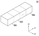
도 3은 도 2의 메모리 셀 어레이의 일 실시 예를 나타낸 도면이다.FIG. 3 is a diagram illustrating an embodiment of the memory cell array of FIG. 2.
도 3을 참조하면, 메모리 셀 어레이(110)는 복수의 메모리 블록들(BLK1~BLKz)을 포함한다. 각 메모리 블록은 3차원 구조를 갖는다. 각 메모리 블록은 기판 위에 적층된 복수의 메모리 셀들을 포함한다. 이러한 복수의 메모리 셀들은 +X 방향, +Y 방향 및 +Z 방향을 따라 배열된다. 각 메모리 블록의 구조는 도 4 및 도 5를 참조하여 더 상세히 설명된다.Referring to FIG. 3, the
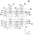
도 4는 도 3의 메모리 블록들(BLK1~BLKz) 중 어느 하나의 메모리 블록(BLKa)을 보여주는 회로도이다.4 is a circuit diagram of one of the memory blocks BLK1 to BLKz of FIG. 3 showing a memory block BLKa.
도 4를 참조하면 메모리 블록(BLKa)은 복수의 셀 스트링들(CS11~CS1m, CS21~CS2m)을 포함한다. 실시 예로서, 복수의 셀 스트링들(CS11~CS1m, CS21~CS2m) 각각은 'U'자형으로 형성될 수 있다. 메모리 블록(BLKa) 내에서, 행 방향(즉 +X 방향)으로 m개의 셀 스트링들이 배열된다. 도 5에서, 열 방향(즉 +Y 방향)으로 2개의 셀 스트링들이 배열되는 것으로 도시되었다. 하지만 이는 설명의 편의를 위한 것으로서 열 방향으로 3개 이상의 셀 스트링들이 배열될 수 있음이 이해될 것이다.Referring to FIG. 4, the memory block BLKa includes a plurality of cell strings CS11 to CS1m and CS21 to CS2m. As an embodiment, each of the plurality of cell strings CS11 to CS1m and CS21 to CS2m may be formed in an'U' shape. In the memory block BLKa, m cell strings are arranged in a row direction (ie +X direction). In FIG. 5, it is shown that two cell strings are arranged in the column direction (ie +Y direction). However, it will be understood that three or more cell strings may be arranged in a column direction for convenience of description.
복수의 셀 스트링들(CS11~CS1m, CS21~CS2m) 각각은 적어도 하나의 소스 선택 트랜지스터(SST), 제1 내지 제 n 메모리 셀들(MC1~MCn), 파이프 트랜지스터(PT), 그리고 적어도 하나의 드레인 선택 트랜지스터(DST)를 포함한다.Each of the plurality of cell strings CS11 to CS1m and CS21 to CS2m includes at least one source select transistor SST, first to nth memory cells MC1 to MCn, pipe transistor PT, and at least one drain And a selection transistor DST.
선택 트랜지스터들(SST, DST) 및 메모리 셀들(MC1~MCn) 각각은 유사한 구조를 가질 수 있다. 실시 예로서, 선택 트랜지스터들(SST, DST) 및 메모리 셀들(MC1~MCn) 각각은 채널층, 터널링 절연막, 전하 저장막 및 블로킹 절연막을 포함할 수 있다. 실시 예로서, 채널층을 제공하기 위한 필라(pillar)가 각 셀 스트링(each cell string)에 제공될 수 있다. 실시 예로서, 채널층, 터널링 절연막, 전하 저장막 및 블로킹 절연막 중 적어도 하나를 제공하기 위한 필라가 각 셀 스트링에 제공될 수 있다.Each of the selection transistors SST and DST and the memory cells MC1 to MCn may have a similar structure. As an embodiment, each of the selection transistors SST and DST and the memory cells MC1 to MCn may include a channel layer, a tunneling insulating layer, a charge storage layer, and a blocking insulating layer. As an embodiment, a pillar for providing a channel layer may be provided in each cell string. As an embodiment, a pillar for providing at least one of a channel layer, a tunneling insulating layer, a charge storage layer, and a blocking insulating layer may be provided in each cell string.
각 셀 스트링의 소스 선택 트랜지스터(SST)는 공통 소스 라인(CSL)과 메모리 셀들(MC1~MCp) 사이에 연결된다.The source select transistor SST of each cell string is connected between the common source line CSL and the memory cells MC1 to MCp.
실시 예로서, 동일한 행에 배열된 셀 스트링들의 소스 선택 트랜지스터들은 행 방향으로 신장되는 소스 선택 라인에 연결되고, 상이한 행에 배열된 셀 스트링들의 소스 선택 트랜지스터들은 상이한 소스 선택 라인들에 연결된다. 도 4에서, 제1 행의 셀 스트링들(CS11~CS1m)의 소스 선택 트랜지스터들은 제1 소스 선택 라인(SSL1)에 연결되어 있다. 제 2 행의 셀 스트링들(CS21~CS2m)의 소스 선택 트랜지스터들은 제 2 소스 선택 라인(SSL2)에 연결되어 있다.As an embodiment, source select transistors of cell strings arranged in the same row are connected to a source select line extending in the row direction, and source select transistors of cell strings arranged in different rows are connected to different source select lines. In FIG. 4, source select transistors of the cell strings CS11 to CS1m of the first row are connected to the first source select line SSL1. The source select transistors of the cell strings CS21 to CS2m in the second row are connected to the second source select line SSL2.
다른 실시 예로서, 셀 스트링들(CS11~CS1m, CS21~CS2m)의 소스 선택 트랜지스터들은 하나의 소스 선택 라인에 공통 연결될 수 있다.As another example, source select transistors of the cell strings CS11 to CS1m and CS21 to CS2m may be commonly connected to one source select line.
각 셀 스트링의 제1 내지 제 n 메모리 셀들(MC1~MCn)은 소스 선택 트랜지스터(SST)와 드레인 선택 트랜지스터(DST) 사이에 연결된다.The first to nth memory cells MC1 to MCn of each cell string are connected between the source select transistor SST and the drain select transistor DST.
제1 내지 제 n 메모리 셀들(MC1~MCn)은 제1 내지 제 p 메모리 셀들(MC1~MCp)과 제 p+1 내지 제 n 메모리 셀들(MCp+1~MCn)로 구분될 수 있다. 제1 내지 제 p 메모리 셀들(MC1~MCp)은 +Z 방향과 역방향으로 순차적으로 배열되며, 소스 선택 트랜지스터(SST)와 파이프 트랜지스터(PT) 사이에서 직렬 연결된다. 제 p+1 내지 제 n 메모리 셀들(MCp+1~MCn)은 +Z 방향으로 순차적으로 배열되며, 파이프 트랜지스터(PT)와 드레인 선택 트랜지스터(DST) 사이에서 직렬 연결된다. 제1 내지 제 p 메모리 셀들(MC1~MCp)과 제 p+1 내지 제 n 메모리 셀들(MCp+1~MCn)은 파이프 트랜지스터(PT)를 통해 연결된다. 각 셀 스트링의 제1 내지 제 n 메모리 셀들(MC1~MCn)의 게이트들은 각각 제1 내지 제 n 워드라인들(WL1~WLn)에 연결된다.The first to nth memory cells MC1 to MCn may be divided into first to pth memory cells MC1 to MCp and p+1 to nth memory cells MCp+1 to MCn. The first to p-th memory cells MC1 to MCp are sequentially arranged in the +Z direction and the reverse direction, and are connected in series between the source select transistor SST and the pipe transistor PT. The p+1 to n-th memory cells MCp+1 to MCn are sequentially arranged in the +Z direction, and are serially connected between the pipe transistor PT and the drain select transistor DST. The first to pth memory cells MC1 to MCp and the p+1 to nth memory cells MCp+1 to MCn are connected through a pipe transistor PT. Gates of the first to nth memory cells MC1 to MCn of each cell string are respectively connected to the first to nth word lines WL1 to WLn.
각 셀 스트링의 파이프 트랜지스터(PT)의 게이트는 파이프 라인(PL)에 연결된다.The gate of the pipe transistor PT of each cell string is connected to the pipeline PL.
각 셀 스트링의 드레인 선택 트랜지스터(DST)는 해당 비트라인과 메모리 셀들(MCp+1~MCn) 사이에 연결된다. 행 방향으로 배열되는 셀 스트링들은 행 방향으로 신장되는 드레인 선택 라인에 연결된다. 제1 행의 셀 스트링들(CS11~CS1m)의 드레인 선택 트랜지스터들은 제1 드레인 선택 라인(DSL1)에 연결된다. 제 2 행의 셀 스트링들(CS21~CS2m)의 드레인 선택 트랜지스터들은 제 2 드레인 선택 라인(DSL2)에 연결된다.The drain select transistor DST of each cell string is connected between a corresponding bit line and memory cells MCp+1 to MCn. Cell strings arranged in the row direction are connected to a drain select line extending in the row direction. The drain select transistors of the cell strings CS11 to CS1m in the first row are connected to the first drain select line DSL1. The drain select transistors of the cell strings CS21 to CS2m in the second row are connected to the second drain select line DSL2.
열 방향으로 배열되는 셀 스트링들은 열 방향으로 신장되는 비트라인에 연결된다. 도 4에서, 제1 열의 셀 스트링들(CS11, CS21)은 제1 비트라인(BL1)에 연결되어 있다. 제 m 열의 셀 스트링들(CS1m, CS2m)은 제 m 비트라인(BLm)에 연결되어 있다.Cell strings arranged in the column direction are connected to bit lines extending in the column direction. In FIG. 4, the cell strings CS11 and CS21 of the first column are connected to the first bit line BL1. The cell strings CS1m and CS2m of the m-th column are connected to the m-th bit line BLm.
행 방향으로 배열되는 셀 스트링들 내에서 동일한 워드라인에 연결되는 메모리 셀들은 하나의 페이지를 구성한다. 예를 들면, 제1 행의 셀 스트링들(CS11~CS1m) 중 제1 워드라인(WL1)과 연결된 메모리 셀들은 하나의 페이지를 구성한다. 제 2 행의 셀 스트링들(CS21~CS2m) 중 제1 워드라인(WL1)과 연결된 메모리 셀들은 다른 하나의 페이지를 구성한다. 드레인 선택 라인들(DSL1, DSL2) 중 어느 하나가 선택됨으로써 하나의 행 방향으로 배열되는 셀 스트링들이 선택될 것이다. 워드라인들(WL1~WLn) 중 어느 하나가 선택됨으로써 선택된 셀 스트링들 중 하나의 페이지가 선택될 것이다.Memory cells connected to the same word line in cell strings arranged in a row direction constitute one page. For example, the memory cells connected to the first word line WL1 among the cell strings CS11 to CS1m of the first row constitute one page. The memory cells connected to the first word line WL1 among the cell strings CS21 to CS2m of the second row constitute another page. Cell strings arranged in one row direction may be selected by selecting one of the drain select lines DSL1 and DSL2. By selecting one of the word lines WL1 to WLn, one page of the selected cell strings will be selected.
다른 실시 예로서, 제1 내지 제 m 비트라인들(BL1~BLm) 대신 이븐 비트라인들 및 오드 비트라인들이 제공될 수 있다. 그리고 행 방향으로 배열되는 셀 스트링들(CS11~CS1m 또는 CS21~CS2m) 중 짝수 번째 셀 스트링들은 이븐 비트라인들에 각각 연결되고, 행 방향으로 배열되는 셀 스트링들(CS11~CS1m 또는 CS21~CS2m) 중 홀수 번째 셀 스트링들은 오드 비트라인들에 각각 연결될 수 있다.As another embodiment, even bit lines and odd bit lines may be provided instead of the first to m-th bit lines BL1 to BLm. Further, even-numbered cell strings among the cell strings CS11 to CS1m or CS21 to CS2m arranged in the row direction are connected to even bit lines, respectively, and cell strings CS11 to CS1m or CS21 to CS2m arranged in the row direction. The odd-numbered cell strings may be connected to odd bit lines, respectively.
실시 예로서, 제1 내지 제 n 메모리 셀들(MC1~MCn) 중 적어도 하나 이상은 더미 메모리 셀로서 이용될 수 있다. 예를 들어, 적어도 하나 이상의 더미 메모리 셀들은 소스 선택 트랜지스터(SST)와 메모리 셀들(MC1~MCp) 사이의 전계(electric field)를 감소시키기 위해 제공된다. 또는, 적어도 하나 이상의 더미 메모리 셀들은 드레인 선택 트랜지스터(DST)와 메모리 셀들(MCp+1~MCn) 사이의 전계를 감소시키기 위해 제공된다. 더 많은 더미 메모리 셀들이 제공될수록, 메모리 블록(BLKa)에 대한 동작의 신뢰성이 향상되는 반면, 메모리 블록(BLKa)의 크기는 증가한다. 더 적은 메모리 셀들이 제공될수록, 메모리 블록(BLKa)의 크기는 감소하는 반면 메모리 블록(BLKa)에 대한 동작의 신뢰성은 저하될 수 있다.As an embodiment, at least one of the first to nth memory cells MC1 to MCn may be used as a dummy memory cell. For example, at least one dummy memory cell is provided to reduce the electric field between the source select transistor SST and the memory cells MC1 to MCp. Alternatively, at least one dummy memory cell is provided to reduce the electric field between the drain select transistor DST and the memory cells MCp+1 to MCn. The more dummy memory cells are provided, the more reliable the operation of the memory block BLKa is, while the size of the memory block BLKa is increased. As fewer memory cells are provided, the size of the memory block BLKa decreases while reliability of operation of the memory block BLKa decreases.
적어도 하나 이상의 더미 메모리 셀들을 효율적으로 제어하기 위해, 더미 메모리 셀들 각각은 요구되는 문턱전압을 가질 수 있다. 메모리 블록(BLKa)에 대한 소거 동작 이전 또는 이후에, 더미 메모리 셀들 중 전부 혹은 일부에 대한 프로그램 동작들이 수행될 수 있다. 프로그램 동작이 수행된 뒤에 소거 동작이 수행되는 경우, 더미 메모리 셀들의 문턱전압은 각각의 더미 메모리 셀들에 연결된 더미 워드라인들에 인가되는 전압을 제어함으로써 더미 메모리 셀들은 요구되는 문턱전압을 가질 수 있다.To efficiently control the at least one dummy memory cell, each of the dummy memory cells may have a required threshold voltage. Before or after the erase operation on the memory block BLKa, program operations on all or part of the dummy memory cells may be performed. When the erase operation is performed after the program operation is performed, the threshold voltages of the dummy memory cells control the voltage applied to the dummy word lines connected to the dummy memory cells, so that the dummy memory cells can have the required threshold voltage. .
도 5는 도 3의 메모리 블록들(BLK1~BLKz) 중 어느 하나의 메모리 블록(BLKb)의 다른 실시 예를 보여주는 회로도이다.FIG. 5 is a circuit diagram illustrating another embodiment of one of the memory blocks BLK1 to BLKz of FIG. 3.
도 5를 참조하면 메모리 블록(BLKb)은 복수의 셀 스트링들(CS11'~CS1m', CS21'~CS2m')을 포함한다. 복수의 셀 스트링들(CS11'~CS1m', CS21'~CS2m') 각각은 +Z 방향을 따라 신장된다. 복수의 셀 스트링들(CS11'~CS1m', CS21'~CS2m') 각각은, 메모리 블록(BLK1') 하부의 기판(미도시) 위에 적층된, 적어도 하나의 소스 선택 트랜지스터(SST), 제1 내지 제 n 메모리 셀들(MC1~MCn) 그리고 적어도 하나의 드레인 선택 트랜지스터(DST)를 포함한다.Referring to FIG. 5, the memory block BLKb includes a plurality of cell strings CS11' to CS1m' and CS21' to CS2m'. Each of the plurality of cell strings CS11' to CS1m' and CS21' to CS2m' extends along the +Z direction. Each of the plurality of cell strings CS11' to CS1m' and CS21' to CS2m' is stacked on a substrate (not shown) under the memory block BLK1', at least one source selection transistor SST, first To n-th memory cells MC1 to MCn and at least one drain select transistor DST.
각 셀 스트링의 소스 선택 트랜지스터(SST)는 공통 소스 라인(CSL)과 메모리 셀들(MC1~MCn) 사이에 연결된다. 동일한 행에 배열된 셀 스트링들의 소스 선택 트랜지스터들은 동일한 소스 선택 라인에 연결된다. 제1 행에 배열된 셀 스트링들(CS11'~CS1m')의 소스 선택 트랜지스터들은 제1 소스 선택 라인(SSL1)에 연결된다. 제 2 행에 배열된 셀 스트링들(CS21'~CS2m')의 소스 선택 트랜지스터들은 제 2 소스 선택 라인(SSL2)에 연결된다. 다른 실시 예로서, 셀 스트링들(CS11'~CS1m', CS21'~CS2m')의 소스 선택 트랜지스터들은 하나의 소스 선택 라인에 공통 연결될 수 있다.The source select transistor SST of each cell string is connected between the common source line CSL and the memory cells MC1 to MCn. Source select transistors of cell strings arranged in the same row are connected to the same source select line. The source select transistors of the cell strings CS11' to CS1m' arranged in the first row are connected to the first source select line SSL1. The source select transistors of the cell strings CS21' to CS2m' arranged in the second row are connected to the second source select line SSL2. As another embodiment, the source select transistors of the cell strings CS11' to CS1m' and CS21' to CS2m' may be commonly connected to one source select line.
각 셀 스트링의 제1 내지 제 n 메모리 셀들(MC1~MCn)은 소스 선택 트랜지스터(SST)와 드레인 선택 트랜지스터(DST) 사이에서 직렬 연결된다. 제1 내지 제 n 메모리 셀들(MC1~MCn)의 게이트들은 각각 제1 내지 제 n 워드라인들(WL1~WLn)에 연결된다.The first to nth memory cells MC1 to MCn of each cell string are connected in series between the source select transistor SST and the drain select transistor DST. Gates of the first to nth memory cells MC1 to MCn are respectively connected to the first to nth word lines WL1 to WLn.
각 셀 스트링의 드레인 선택 트랜지스터(DST)는 해당 비트라인과 메모리 셀들(MC1~MCn) 사이에 연결된다. 행 방향으로 배열되는 셀 스트링들의 드레인 선택 트랜지스터들은 행 방향으로 신장되는 드레인 선택 라인에 연결된다. 제1 행의 셀 스트링들(CS11'~CS1m')의 드레인 선택 트랜지스터들은 제1 드레인 선택 라인(DSL1)에 연결된다. 제 2 행의 셀 스트링들(CS21'~CS2m')의 드레인 선택 트랜지스터들은 제 2 드레인 선택 라인(DSL2)에 연결된다.The drain select transistor DST of each cell string is connected between the corresponding bit line and the memory cells MC1 to MCn. The drain select transistors of the cell strings arranged in the row direction are connected to the drain select line extending in the row direction. The drain select transistors of the cell strings CS11' to CS1m' of the first row are connected to the first drain select line DSL1. The drain select transistors of the cell strings CS21' to CS2m' of the second row are connected to the second drain select line DSL2.
결과적으로, 각 셀 스트링에 파이프 트랜지스터(PT)가 제외된 것을 제외하면 도 5의 메모리 블록(BLKb)은 도 4의 메모리 블록(BLKa)과 유사한 등가 회로를 갖는다.As a result, the memory block BLKb of FIG. 5 has an equivalent circuit similar to the memory block BLKa of FIG. 4 except that the pipe transistor PT is excluded from each cell string.
다른 실시 예로서, 제1 내지 제 m 비트라인들(BL1~BLm) 대신 이븐 비트라인들 및 오드 비트라인들이 제공될 수 있다. 그리고 행 방향으로 배열되는 셀 스트링들(CS11'~CS1m' 또는 CS21'~CS2m') 중 짝수 번째 셀 스트링들은 이븐 비트라인들에 각각 연결되고, 행 방향으로 배열되는 셀 스트링들(CS11'~CS1m' 또는 CS21'~CS2m') 중 홀수 번째 셀 스트링들은 오드 비트라인들에 각각 연결될 수 있다.As another embodiment, even bit lines and odd bit lines may be provided instead of the first to m-th bit lines BL1 to BLm. Further, even-numbered cell strings among the cell strings CS11' to CS1m' or CS21' to CS2m' arranged in the row direction are connected to even bit lines, respectively, and the cell strings CS11' to CS1m arranged in the row direction. 'Or CS21' to CS2m'), odd-numbered cell strings may be connected to odd bit lines, respectively.
실시 예로서, 제1 내지 제 n 메모리 셀들(MC1~MCn) 중 적어도 하나 이상은 더미 메모리 셀로서 이용될 수 있다. 예를 들어, 적어도 하나 이상의 더미 메모리 셀들은 소스 선택 트랜지스터(SST)와 메모리 셀들(MC1~MCn) 사이의 전계(electric field)를 감소시키기 위해 제공된다. 또는, 적어도 하나 이상의 더미 메모리 셀들은 드레인 선택 트랜지스터(DST)와 메모리 셀들(MC1~MCn) 사이의 전계를 감소시키기 위해 제공된다. 더 많은 더미 메모리 셀들이 제공될수록, 메모리 블록(BLKb)에 대한 동작의 신뢰성이 향상되는 반면, 메모리 블록(BLKb)의 크기는 증가한다. 더 적은 메모리 셀들이 제공될수록, 메모리 블록(BLKb)의 크기는 감소하는 반면 메모리 블록(BLKb)에 대한 동작의 신뢰성은 저하될 수 있다.As an embodiment, at least one of the first to nth memory cells MC1 to MCn may be used as a dummy memory cell. For example, at least one dummy memory cell is provided to reduce the electric field between the source select transistor SST and the memory cells MC1 to MCn. Alternatively, at least one dummy memory cell is provided to reduce the electric field between the drain select transistor DST and the memory cells MC1 to MCn. The more dummy memory cells are provided, the more reliable the operation of the memory block BLKb is, while the size of the memory block BLKb is increased. As fewer memory cells are provided, the size of the memory block BLKb decreases while reliability of operation of the memory block BLKb may deteriorate.
적어도 하나 이상의 더미 메모리 셀들을 효율적으로 제어하기 위해, 더미 메모리 셀들 각각은 요구되는 문턱전압을 가질 수 있다. 메모리 블록(BLKb)에 대한 소거 동작 이전 또는 이후에, 더미 메모리 셀들 중 전부 혹은 일부에 대한 프로그램 동작들이 수행될 수 있다. 프로그램 동작이 수행된 뒤에 소거 동작이 수행되는 경우, 더미 메모리 셀들의 문턱전압은 각각의 더미 메모리 셀들에 연결된 더미 워드라인들에 인가되는 전압을 제어함으로써 더미 메모리 셀들은 요구되는 문턱전압을 가질 수 있다.To efficiently control the at least one dummy memory cell, each of the dummy memory cells may have a required threshold voltage. Before or after the erase operation on the memory block BLKb, program operations on all or part of the dummy memory cells may be performed. When the erase operation is performed after the program operation is performed, the threshold voltages of the dummy memory cells control the voltage applied to the dummy word lines connected to the dummy memory cells, so that the dummy memory cells can have the required threshold voltage. .
도 6은 실시 예에 따른 메모리 컨트롤러의 구성 및 동작을 설명하기 위한 도면이다.6 is a view for explaining the configuration and operation of a memory controller according to an embodiment.
도 6을 참조하면, 메모리 컨트롤러(200)는 입력 데이터 제어부(210), 시퀀스 정보 생성부(220), 쓰기 동작 제어부(230) 및 매핑 테이블(240)을 포함할 수 있다.Referring to FIG. 6, the
실시 예에서, 입력 데이터 제어부(210)는 도 1을 참조하여 설명된 호스트로부터 메모리 장치(100)에 저장할 데이터와 저장할 데이터의 논리 주소를 제공받을 수 있다. 구체적으로, 입력 데이터 제어부(210)는 호스트로부터 메모리 장치(100)에 포함된 복수의 페이지들 중 선택된 페이지에 저장할 데이터를 제공받을 수 있다. 호스트로부터 제공받은 저장할 데이터는 수신 데이터일 수 있다.In an embodiment, the input
다른 실시 예에서, 입력 데이터 제어부(210)는 메모리 장치(100)로부터 메모리 장치(100)에 저장할 데이터를 제공받을 수 있다. 구체적으로, 입력 데이터 제어부(210)는 메모리 장치(100)로부터 메모리 장치(100)에 포함된 복수의 페이지들 중 선택된 페이지에 저장할 데이터를 제공받을 수 있다. 메모리 장치(100)로부터 제공받은 데이터는 복수의 페이지들 중 선택된 페이지와 다른 페이지에 저장된 데이터가 리드된 데이터일 수 있다.In another embodiment, the input
입력 데이터 제어부(210)는 입력 데이터를 쓰기 동작 제어부(230)에 제공할 수 있다. 입력 데이터는 입력 데이터 제어부(210)가 호스트 또는 메모리 장치(100)로부터 제공받은 메모리 장치(100)에 저장될 데이터일 수 있다. 실시 예에서, 입력 데이터는 메모리 장치(100)에 포함된 복수의 페이지들 중 선택된 페이지에 저장될 데이터일 수 있다.The input
입력 데이터 제어부(210)는 매핑 테이블(240)을 참조하여 입력 데이터가 저장될 메모리 장치(100)의 물리 주소를 쓰기 동작 제어부(230)에 제공할 수 있다. 실시 예에서, 물리 주소는 입력 데이터가 저장될 선택된 페이지의 물리 주소일 수 있다. The input
시퀀스 정보 생성부(220)는 카운트 회로(221)를 포함할 수 있다. 카운트 회로(221)는 쓰기 동작 제어부(230)가 제공하는 프로그램 동작 수행 정보를 기초로, 메모리 장치(100)에 의해 수행된 프로그램 동작들의 총 횟수를 카운트할 수 있다.The
실시 예에서, 시퀀스 정보 생성부(220)는 메모리 장치(100)의 동작 상태를 반영하여 선택된 페이지에 입력 데이터를 저장하는 프로그램 동작이 수행될 순번을 결정할 수 있다. 시퀀스 정보 생성부(220)는 카운트한 프로그램 동작의 총 횟수를 기초로 프로그램 동작이 수행될 순번을 결정할 수 있다. 시퀀스 정보 생성부(220)는 결정한 순번을 나타내는 시퀀스 정보를 생성할 수 있다.In an embodiment, the sequence
쓰기 동작 제어부(230)는 입력 데이터를 메모리 장치(100)에 포함된 복수의 페이지들에 저장하도록 메모리 장치(100)를 제어할 수 있다. 구체적으로, 쓰기 동작 제어부(230)는 입력 데이터를 메모리 장치(100)에 포함된 복수의 페이지들 중 선택된 페이지의 메인 영역에 저장하고, 히스토리 정보를 선택된 페이지의 스페어 영역에 저장하는 프로그램 커맨드를 메모리 장치(100)에 제공할 수 있다.The write
히스토리 정보는 입력 데이터의 논리 주소를 포함할 수 있다. 히스토리 정보는 입력 데이터가 저장될 선택된 페이지의 물리 주소 및 입력 데이터에 대응되는 시퀀스 정보를 포함할 수 있다. The history information may include a logical address of input data. The history information may include a physical address of a selected page in which input data is to be stored and sequence information corresponding to the input data.
쓰기 동작 제어부(230)는 메모리 장치(100)에 의해 입력 데이터를 저장하는 프로그램 동작이 수행되었음을 나타내는 프로그램 동작 수행 정보를 생성할 수 있다.The write
매핑 테이블(240)은 입력 데이터의 논리 주소와 대응되는 물리 주소를 포함할 수 있다. 물리 주소는 입력 데이터가 저장될 메모리 장치(100)의 물리 주소일 수 있다. 물리 주소는 입력 데이터가 저장될 선택된 페이지의 물리 주소일 수 있다. 물리 주소는 선택된 페이지를 포함하는 메모리 블록을 지시하는 블록 인덱스와 메모리 블록에 포함된 복수의 페이지들 중 선택된 페이지를 지시하는 페이지 인덱스를 포함할 수 있다.The mapping table 240 may include a physical address corresponding to a logical address of input data. The physical address may be a physical address of the
다른 실시 예에서, 입력 데이터가 복수의 페이지들로 나뉘어 저장되는 경우, 입력 데이터 제어부(210)는 입력 데이터를 페이지 단위로 저장되는 적어도 하나의 입력 데이터 청크로 구분할 수 있다. 시퀀스 정보 생성부(220)는 적어도 하나의 입력 데이터 청크 중 어느 하나의 데이터 청크에 대응되는 청크 시퀀스 정보를 생성할 수 있다. In another embodiment, when the input data is divided into a plurality of pages and stored, the
청크 시퀀스 정보는 복수의 페이지들 중 선택된 페이지에 어느 하나의 데이터 청크를 저장하는 프로그램 동작이 수행될 순번을 나타내는 정보일 수 있다. 시퀀스 정보 생성부(220)는 메모리 장치에 의해 수행된 프로그램 동작들의 총 횟수에 따라 청크 시퀀스 정보를 결정할 수 있다.The chunk sequence information may be information indicating a sequence number in which a program operation for storing one chunk of data in a selected page among a plurality of pages is performed. The
쓰기 동작 제어부(230)는 어느 하나의 데이터 청크를 선택된 페이지의 메인 영역에 저장하고, 히스토리 정보를 선택된 페이지의 스페어 영역에 저장하는 프로그램 동작을 지시하는 프로그램 커맨드를 메모리 장치(100)에 제공할 수 있다. 히스토리 정보는 선택된 페이지의 물리 주소 및 어느 하나의 데이터 청크에 대응되는 청크 시퀀스 정보를 포함할 수 있다.The write
다른 실시 예에서, 하나의 페이지는 복수의 서브 페이지들을 포함할 수 있다. 복수의 서브 페이지들 각각은 메인 영역 및 스페어 영역을 포함할 수 있다. 데이터를 리드하거나 프로그램 하는 동작은 서브 페이지 단위로 수행될 수 있다.In another embodiment, one page may include a plurality of sub pages. Each of the plurality of sub pages may include a main area and a spare area. The operation of reading or programming data may be performed in units of sub pages.
입력 데이터 제어부(210)는 입력 데이터를 서브 페이지 단위로 저장되는 적어도 하나의 입력 데이터 청크로 구분할 수 있다. 시퀀스 정보 생성부(220)는 적어도 하나의 입력 데이터 청크 중 어느 하나의 데이터 청크에 대응되는 청크 시퀀스 정보를 생성할 수 있다. The input
청크 시퀀스 정보는 선택된 페이지에 포함되는 복수의 서브 페이지들 중 선택된 서브 페이지에 어느 하나의 데이터 청크를 저장하는 프로그램 동작이 수행될 순번을 나타내는 정보일 수 있다. 청크 시퀀스 정보는 메모리 장치에 의해 수행된 프로그램 동작들의 총 횟수에 따라 결정될 수 있다.The chunk sequence information may be information indicating a sequence number in which a program operation for storing one data chunk in a selected subpage among a plurality of subpages included in the selected page will be performed. The chunk sequence information may be determined according to the total number of program operations performed by the memory device.
쓰기 동작 제어부(230)는 어느 하나의 데이터 청크를 선택된 서브 페이지의 메인 영역에 저장하도록 메모리 장치(100)를 제어할 수 있다. 쓰기 동작 제어부(230)는 선택된 서브 페이지의 물리 주소 및 청크 시퀀스 정보를 포함하는 히스토리 정보를 선택된 서브 페이지의 스페어 영역에 저장하도록 메모리 장치(100)를 제어할 수 있다.The
도 7은 도 2의 물리 페이지를 설명하기 위한 도면이다.FIG. 7 is a diagram for explaining the physical page of FIG. 2.
도 7을 참조하면, 하나의 물리 페이지는 도 2를 참조하여 설명된 하나의 워드라인에 연결된 복수의 메모리 셀들이 데이터를 저장하는 단위일 수 있다. 물리 페이지는 메인 영역과 스페어 영역을 포함할 수 있다. 메인 영역은 유저 데이터를 저장하는 영역이고, 스페어 영역은 유저 데이터와 관련된 정보를 저장하는 영역일 수 있다. Referring to FIG. 7, one physical page may be a unit in which a plurality of memory cells connected to one word line described with reference to FIG. 2 stores data. The physical page may include a main area and a spare area. The main area may be an area for storing user data, and the spare area may be an area for storing information related to user data.
실시 예에서, 유저 데이터는 물리 페이지의 메인 영역에 저장될 수 있다. 유저 데이터의 논리 주소는 물리 페이지의 스페어 영역에 저장될 수 있다. 유저 데이터의 논리 주소는 도 1을 참조하여 설명된 호스트로부터 제공될 수 있다.In an embodiment, user data may be stored in the main area of the physical page. The logical address of the user data may be stored in the spare area of the physical page. The logical address of the user data can be provided from the host described with reference to FIG. 1.
도 6을 참조하여 설명된 히스토리 정보는 물리 페이지의 스페어 영역에 저장될 수 있다. 히스토리 정보는 유저 데이터가 저장될 물리 페이지의 물리 주소를 포함할 수 있다. 히스토리 정보는 유저 데이터에 대응되는 시퀀스 정보를 포함할 수 있다. 시퀀스 정보는 물리 페이지에 유저 데이터를 저장하는 프로그램 동작이 수행될 순번을 나타내는 정보일 수 있다. 시퀀스 정보는 메모리 장치에 의해 수행된 프로그램 동작들의 총 횟수에 따라 결정될 수 있다. The history information described with reference to FIG. 6 may be stored in the spare area of the physical page. The history information may include a physical address of a physical page in which user data will be stored. The history information may include sequence information corresponding to user data. The sequence information may be information indicating a sequence number in which a program operation for storing user data in a physical page is performed. The sequence information may be determined according to the total number of program operations performed by the memory device.
도 8은 도 2의 물리 페이지의 다른 실시 예를 설명하기 위한 도면이다.8 is a view for explaining another embodiment of the physical page of FIG. 2.
도 8을 참조하면, 도 7의 물리 페이지와 대비하여 하나의 물리 페이지는 복수의 서브 페이지들을 포함할 수 있다. 복수의 서브 페이지들 각각은 메인 영역 및 스페어 영역을 포함할 수 있다. 데이터를 리드하거나 프로그램 하는 동작은 서브 페이지 단위로 수행될 수 있다.Referring to FIG. 8, in contrast to the physical page of FIG. 7, one physical page may include a plurality of sub pages. Each of the plurality of sub pages may include a main area and a spare area. The operation of reading or programming data may be performed in units of sub pages.
실시 예에서, 물리 페이지는 서브 페이지 1 및 서브 페이지 2를 포함할 수 있다. 하나의 물리 페이지가 포함하는 서브 페이지의 개수는 본 실시 예에 제한되지 않는다. In an embodiment, the physical page may include sub-page 1 and
도 7에서 설명된 바와 유사하게, 유저 데이터는 하나의 서브 페이지의 메인 영역에 저장될 수 있다. 유저 데이터에 대응되는 히스토리 정보는 서브 페이지의 스페어 영역에 저장될 수 있다. 히스토리 정보는 유저 데이터가 저장될 서브 페이지의 물리 주소와 유저 데이터에 대응되는 시퀀스 정보를 포함할 수 있다.Similar to that described in FIG. 7, user data may be stored in the main area of one sub-page. History information corresponding to user data may be stored in a spare area of a sub page. The history information may include physical addresses of sub-pages in which user data will be stored and sequence information corresponding to user data.
실시 예에서, 서브 페이지의 물리 주소는, 선택된 페이지를 포함하는 메모리 블록을 지시하는 블록 인덱스와 메모리 블록에 포함된 복수의 페이지들 중 선택된 페이지를 지시하는 페이지 인덱스를 포함할 수 있다. 선택된 페이지는 서브 페이지를 포함하는 물리 페이지일 수 있다. 다른 실시 예에서, 서브 페이지의 물리 주소는 앞에서 설명된 블록 인덱스 및 페이지 인덱스를 포함하고, 선택된 페이지에 포함된 복수의 서브 페이지들 중 유저 데이터가 저장되는 서브 페이지를 지시하는 서브 페이지 인덱스를 추가로 포함할 수 있다.In an embodiment, the physical address of the sub-page may include a block index indicating a memory block including the selected page and a page index indicating a selected page among a plurality of pages included in the memory block. The selected page may be a physical page including sub-pages. In another embodiment, the physical address of the sub-page includes the block index and the page index described above, and further includes a sub-page index indicating a sub-page in which user data is stored among a plurality of sub-pages included in the selected page. It can contain.
도 9는 실시 예에 따른 히스토리 정보를 저장하는 동작을 설명하기 위한 도면이다.9 is a diagram illustrating an operation of storing history information according to an embodiment.
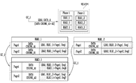
도 9를 참조하면, 메모리 장치는 제1 및 제2 플레인들(Plane 1 및 Plane 2)을 포함할 수 있다. 제1 플레인(Plane 1)은 메모리 블록들(BLK1_1 및 BLK2_1)을 포함할 수 있다. 제2 플레인(Plane 2)은 메모리 블록들(BLK1_2 및 BLK2_2)을 포함할 수 있다. 도 9에서, 메모리 블록들 각각은 제1 및 제2 페이지들(Page1 및 Page2)을 포함할 수 있다.Referring to FIG. 9, the memory device may include first and
하나의 메모리 장치에 포함된 플레인들의 개수, 하나의 플레인에 포함된 메모리 블록들의 개수, 하나의 메모리 블록에 포함된 페이지들의 개수는 본 실시 예에 제한되지 않는다.The number of planes included in one memory device, the number of memory blocks included in one plane, and the number of pages included in one memory block are not limited to this embodiment.
실시 예에서, 메모리 장치는 멀티 플레인 동작을 수행할 수 있다. 멀티 플레인 동작은 서로 다른 플레인에 포함되는 둘 이상의 메모리 블록들에 대해 동시에 데이터를 저장하는 동작일 수 있다. 멀티 플레인 동작은 서로 다른 플레인에 포함되는 둘 이상의 메모리 블록들에 저장된 데이터를 동시에 리드하는 동작일 수 있다. In an embodiment, the memory device may perform a multi-plane operation. The multi-plane operation may be an operation of simultaneously storing data for two or more memory blocks included in different planes. The multi-plane operation may be an operation of simultaneously reading data stored in two or more memory blocks included in different planes.
도 1을 참조하여 설명된 메모리 컨트롤러는 호스트로부터 수신한 쓰기 요청에 따라, 쓰기 데이터를 메모리 장치에 저장하도록 메모리 장치를 제어할 수 있다. 쓰기 데이터는 호스트로부터 제공받은 데이터일 수 있다.The memory controller described with reference to FIG. 1 may control the memory device to store write data in the memory device according to a write request received from the host. The write data may be data provided from the host.
메모리 컨트롤러는 호스트로부터 쓰기 데이터의 논리 주소를 제공받을 수 있다. 메모리 컨트롤러는 쓰기 데이터의 논리 주소와 매핑되는 물리 주소에 쓰기 데이터를 저장하도록 메모리 장치를 제어할 수 있다. 쓰기 데이터의 논리 주소와 매핑되는 물리 주소는 쓰기 데이터가 저장될 메모리 장치의 물리 주소일 수있다.The memory controller may be provided with a logical address of write data from the host. The memory controller may control the memory device to store write data at a physical address mapped to a logical address of write data. The physical address mapped to the logical address of the write data may be a physical address of the memory device in which the write data is stored.
도 9에서, 각 페이지는 도 7에 설명된 물리 페이지와 동일한 구성을 가질 수 있다. 따라서, 각 페이지의 빗금 쳐지지 않은 영역은 메인 영역이고, 빗금 쳐진 영역은 스페어 영역일 수 있다.In FIG. 9, each page may have the same configuration as the physical page described in FIG. Therefore, a non-hatched area of each page may be a main area, and a hatched area may be a spare area.
제 1 쓰기 요청(Write_1)에 따라, 제1 데이터(DATA_A)가 메모리 장치에 저장될 수 있다. 제1 데이터(DATA_A)는 페이지 단위로 저장되는 데이터 청크들(DATA CHUNK_A1~A2)로 구분될 수 있다.According to the first write request (Write_1), the first data DATA_A may be stored in the memory device. The first data DATA_A may be divided into data chunks DATA CHUNK_A1 to A2 stored in units of pages.
메모리 장치의 멀티 플레인 동작에 따라, 메모리 블록(BLK1_1)의 제1 페이지(Page 1)에 데이터 청크(DATA CHUNK_A1)를 저장하는 프로그램 동작과 메모리 블록(BLK1_2)의 제1 페이지(Page 1)에 데이터 청크(DATA CHUNK_A2)를 저장하는 프로그램 동작은 동시에 수행될 수 있다.According to the multi-plane operation of the memory device, a program operation for storing a data chunk (DATA CHUNK_A1) in a first page (Page 1) of the memory block BLK1_1 and data in a first page (Page 1) of the memory block BLK1_2 The program operation for storing the chunk (DATA CHUNK_A2) can be performed simultaneously.
메모리 블록(BLK1_1)의 제1 페이지(Page 1)의 메인 영역에 데이터 청크(DATA CHUNK_A1)가 저장될 수 있다. 메모리 블록(BLK1_1)의 제1 페이지(Page 1)의 스페어 영역에 데이터 청크(DATA CHUNK_A1)에 대응되는 히스토리 정보가 저장될 수 있다.The data chunk DATA CHUNK_A1 may be stored in the main area of the
히스토리 정보는 제1 데이터(DATA_A)의 논리 주소(LBA1)를 포함할 수 있다. 히스토리 정보는 데이터 청크(DATA CHUNK_A1)가 저장된 페이지의 물리 주소(BLK1_1+Page1)를 포함할 수 있다. 데이터 청크(DATA CHUNK_A1)에 대응되는 시퀀스 정보는 1일 수 있다. 메모리 장치에 의해 첫 번째로 수행된 프로그램 동작이기 때문이다.The history information may include the logical address LBA1 of the first data DATA_A. The history information may include a physical address (BLK1_1+Page1) of the page in which the data chunk (DATA CHUNK_A1) is stored. Sequence information corresponding to the data chunk (DATA CHUNK_A1) may be 1. This is because it is the first program operation performed by the memory device.
메모리 블록(BLK1_2)의 제1 페이지(Page 1)의 메인 영역에 데이터 청크(DATA CHUNK_A2)가 저장될 수 있다. 메모리 블록(BLK1_2)의 제1 페이지(Page 1)의 스페어 영역에 데이터 청크(DATA CHUNK_A2)에 대응되는 히스토리 정보가 저장될 수 있다.The data chunk DATA CHUNK_A2 may be stored in the main area of the
히스토리 정보는 제1 데이터(DATA_A)의 논리 주소(LBA1)를 포함할 수 있다. 히스토리 정보는 데이터 청크(DATA CHUNK_A2)가 저장된 페이지의 물리 주소(BLK1_2+Page1)를 포함할 수 있다. 데이터 청크(DATA CHUNK_A2)에 대응되는 시퀀스 정보는 1일 수 있다.The history information may include the logical address LBA1 of the first data DATA_A. The history information may include the physical address (BLK1_2+Page1) of the page in which the data chunk (DATA CHUNK_A2) is stored. Sequence information corresponding to the data chunk (DATA CHUNK_A2) may be 1.
제 2 쓰기 요청(Write_2)에 따라, 제2 데이터(DATA_B)가 메모리 장치에 저장될 수 있다. 제2 데이터(DATA_B)는 페이지 단위로 저장되는 데이터 청크들(DATA CHUNK_B1~B3)로 구분될 수 있다.According to the second write request (Write_2), the second data DATA_B may be stored in the memory device. The second data DATA_B may be divided into data chunks DATA CHUNK_B1 to B3 stored in units of pages.
메모리 장치의 멀티 플레인 동작에 따라, 메모리 블록(BLK1_1)의 제2 페이지(Page 2)에 데이터 청크(DATA CHUNK_B1)를 저장하는 프로그램 동작과 메모리 블록(BLK1_2)의 제2 페이지(Page 2)에 데이터 청크(DATA CHUNK_B2)를 저장하는 프로그램 동작은 동시에 수행될 수 있다.According to the multi-plane operation of the memory device, a program operation for storing a data chunk (DATA CHUNK_B1) in a second page (Page 2) of the memory block BLK1_1 and data in a second page (Page 2) of the memory block BLK1_2 The program operation for storing the chunks (DATA CHUNK_B2) can be performed simultaneously.
메모리 블록(BLK1_1)의 제2 페이지(Page 2)의 메인 영역에 데이터 청크(DATA CHUNK_B1)가 저장될 수 있다. 메모리 블록(BLK1_1)의 제2 페이지(Page 2)의 스페어 영역에 데이터 청크(DATA CHUNK_B1)에 대응되는 히스토리 정보가 저장될 수 있다.The data chunk DATA CHUNK_B1 may be stored in the main area of the
히스토리 정보는 제2 데이터(DATA_B)의 논리 주소(LBA2)를 포함할 수 있다. 히스토리 정보는 데이터 청크(DATA CHUNK_B1)가 저장된 페이지의 물리 주소(BLK1_1+Page2)를 포함할 수 있다. 데이터 청크(DATA CHUNK_B1)에 대응되는 시퀀스 정보는 2일 수 있다. 메모리 장치에 의해 두 번째로 수행된 프로그램 동작이기 때문이다.The history information may include the logical address LBA2 of the second data DATA_B. The history information may include the physical address (BLK1_1+Page2) of the page where the data chunk (DATA CHUNK_B1) is stored. Sequence information corresponding to the data chunk (DATA CHUNK_B1) may be 2. This is because it is the second program operation performed by the memory device.
메모리 블록(BLK1_2)의 제2 페이지(Page 2)의 메인 영역에 데이터 청크(DATA CHUNK_B2)가 저장될 수 있다. 메모리 블록(BLK1_2)의 제2 페이지(Page 2)의 스페어 영역에 데이터 청크(DATA CHUNK_B2)에 대응되는 히스토리 정보가 저장될 수 있다.The data chunk DATA CHUNK_B2 may be stored in the main area of the
히스토리 정보는 제2 데이터(DATA_B)의 논리 주소(LBA2)를 포함할 수 있다. 히스토리 정보는 데이터 청크(DATA CHUNK_B2)가 저장된 페이지의 물리 주소(BLK1_2+Page2)를 포함할 수 있다. 데이터 청크(DATA CHUNK_B2)에 대응되는 시퀀스 정보는 2일 수 있다. The history information may include the logical address LBA2 of the second data DATA_B. The history information may include the physical address (BLK1_2+Page2) of the page in which the data chunk (DATA CHUNK_B2) is stored. Sequence information corresponding to the data chunk (DATA CHUNK_B2) may be 2.
메모리 블록(BLK2_1)의 제1 페이지(Page 1)의 메인 영역에 데이터 청크(DATA CHUNK_B3)가 저장될 수 있다. 메모리 블록(BLK2_1)의 제1 페이지(Page 1)의 스페어 영역에 데이터 청크(DATA CHUNK_B3)에 대응되는 히스토리 정보가 저장될 수 있다.The data chunk DATA CHUNK_B3 may be stored in the main area of the
히스토리 정보는 제2 데이터(DATA_B)의 논리 주소(LBA2)를 포함할 수 있다. 히스토리 정보는 데이터 청크(DATA CHUNK_B3)가 저장된 페이지의 물리 주소(BLK2_1+Page1)를 포함할 수 있다. 데이터 청크(DATA CHUNK_B3)에 대응되는 시퀀스 정보는 3일 수 있다. The history information may include the logical address LBA2 of the second data DATA_B. The history information may include the physical address (BLK2_1+Page1) of the page in which the data chunk (DATA CHUNK_B3) is stored. Sequence information corresponding to the data chunk (DATA CHUNK_B3) may be 3.
제 3 쓰기 요청(Write_3)에 따라, 제3 데이터(DATA_C)가 메모리 장치에 저장될 수 있다. 제3 데이터(DATA_C)는 페이지 단위로 저장되는 데이터 청크들(DATA CHUNK_C1~C3)로 구분될 수 있다.According to the third write request Write_3, the third data DATA_C may be stored in the memory device. The third data DATA_C may be divided into data chunks DATA CHUNK_C1 to C3 stored in units of pages.
메모리 블록(BLK2_2)의 제1 페이지(Page 1)의 메인 영역에 데이터 청크(DATA CHUNK_C1)가 저장될 수 있다. 메모리 블록(BLK2_2)의 제1 페이지(Page 1)의 스페어 영역에 데이터 청크(DATA CHUNK_C1)에 대응되는 히스토리 정보가 저장될 수 있다.The data chunk DATA CHUNK_C1 may be stored in the main area of the
히스토리 정보는 제3 데이터(DATA_C)의 논리 주소(LBA3)를 포함할 수 있다. 히스토리 정보는 데이터 청크(DATA CHUNK_C1)가 저장된 페이지의 물리 주소(BLK2_2+Page1)를 포함할 수 있다. 데이터 청크(DATA CHUNK_ C1)에 대응되는 시퀀스 정보는 4일 수 있다.The history information may include the logical address LBA3 of the third data DATA_C. The history information may include the physical address (BLK2_2+Page1) of the page where the data chunk (DATA CHUNK_C1) is stored. Sequence information corresponding to the data chunk (DATA CHUNK_ C1) may be 4.
메모리 장치의 멀티 플레인 동작에 따라, 메모리 블록(BLK2_1)의 제2 페이지(Page 2)에 데이터 청크(DATA CHUNK_C2)를 저장하는 프로그램 동작과 메모리 블록(BLK2_2)의 제2 페이지(Page 2)에 데이터 청크(DATA CHUNK_C3)를 저장하는 프로그램 동작은 동시에 수행될 수 있다.According to the multi-plane operation of the memory device, a program operation for storing a data chunk (DATA CHUNK_C2) in a second page (Page 2) of the memory block BLK2_1 and data in a second page (Page 2) of the memory block BLK2_2 The program operation for storing the chunks (DATA CHUNK_C3) can be performed simultaneously.
메모리 블록(BLK2_1)의 제2 페이지(Page 2)의 메인 영역에 데이터 청크(DATA CHUNK_C2)가 저장될 수 있다. 메모리 블록(BLK2_1)의 제2 페이지(Page 2)의 스페어 영역에 데이터 청크(DATA CHUNK_C2)에 대응되는 히스토리 정보가 저장될 수 있다.The data chunk DATA CHUNK_C2 may be stored in the main area of the
히스토리 정보는 제3 데이터(DATA_C)의 논리 주소(LBA3)를 포함할 수 있다. 히스토리 정보는 데이터 청크(DATA CHUNK_C2)가 저장된 페이지의 물리 주소(BLK2_1+Page2)를 포함할 수 있다. 데이터 청크(DATA CHUNK_C2)에 대응되는 시퀀스 정보는 5일 수 있다. 메모리 장치에 의해 다섯 번째로 수행된 프로그램 동작이기 때문이다.The history information may include the logical address LBA3 of the third data DATA_C. The history information may include the physical address (BLK2_1+Page2) of the page in which the data chunk (DATA CHUNK_C2) is stored. Sequence information corresponding to the data chunk (DATA CHUNK_C2) may be 5. This is because it is the fifth program operation performed by the memory device.
메모리 블록(BLK2_2)의 제2 페이지(Page 2)의 메인 영역에 데이터 청크(DATA CHUNK_C3)가 저장될 수 있다. 메모리 블록(BLK2_2)의 제2 페이지(Page 2)의 스페어 영역에 데이터 청크(DATA CHUNK_C3)에 대응되는 히스토리 정보가 저장될 수 있다.The data chunk DATA CHUNK_C3 may be stored in the main area of the
히스토리 정보는 제3 데이터(DATA_C)의 논리 주소(LBA3)를 포함할 수 있다. 히스토리 정보는 데이터 청크(DATA CHUNK_C3)가 저장된 페이지의 물리 주소(BLK2_2+Page2)를 포함할 수 있다. 데이터 청크(DATA CHUNK_C3)에 대응되는 시퀀스 정보는 5일 수 있다.The history information may include the logical address LBA3 of the third data DATA_C. The history information may include the physical address (BLK2_2+Page2) of the page in which the data chunk (DATA CHUNK_C3) is stored. Sequence information corresponding to the data chunk (DATA CHUNK_C3) may be 5.
도 10은 실시 예에 따른 히스토리 정보가 갱신되는 동작을 설명하기 위한 도면이다.10 is a diagram for describing an operation in which history information is updated according to an embodiment.
도 9 및 도 10을 참조하면, 메모리 장치는 도 9의 메모리 장치와 비교할 때, 제1 플레인(Plane 1)은 메모리 블록(BLK3_1)을 더 포함할 수 있다. 제2 플레인(Plane 2)은 메모리 블록(BLK3_2)을 더 포함할 수 있다.9 and 10, the memory device may further include a memory block BLK3_1 when compared to the memory device of FIG. 9. The
실시 예에서, 가비지 컬렉션과 같은 백그라운드 동작이 수행될 때, 메모리 장치의 특정 영역에 저장된 데이터는 메모리 장치의 다른 영역에 이동되어 저장될 수 있다. 백그라운드 동작은 도 1을 참조하여 설명된 메모리 컨트롤러의 제어에 따라 호스트의 요청과 무관하게 수행될 수 있다.In an embodiment, when a background operation such as garbage collection is performed, data stored in a specific area of the memory device may be moved and stored in another area of the memory device. The background operation may be performed irrespective of the host request under the control of the memory controller described with reference to FIG. 1.
제1 가비지 컬렉션 동작(GC1)에 따라, 메모리 블록(BLK1_1)의 제1 페이지(Page 1)의 메인 영역에 저장된 데이터 청크(DATA CHUNK_A1)는 메모리 블록(BLK3_1)의 제1 페이지(Page 1)의 메인 영역에 저장될 수 있다.According to the first garbage collection operation GC1, the data chunk DATA CHUNK_A1 stored in the main area of the first page (Page 1) of the memory block BLK1_1 is the first page (Page 1) of the memory block BLK3_1. It can be stored in the main area.
메모리 블록(BLK3_1)의 제1 페이지(Page 1)의 스페어 영역에는 데이터 청크(DATA CHUNK_A1)에 대응되는 이전 히스토리 정보(BLK1_1+Page1, Seq1)가 저장될 수 있다. 메모리 블록(BLK3_1)의 제1 페이지(Page 1)의 스페어 영역에는 데이터 청크(DATA CHUNK_A1)에 대응되는 현재 히스토리 정보(BLK3_1+Page1, Seq6)가 저장될 수 있다.In the spare area of the first page (Page 1) of the memory block BLK3_1, previous history information BLK1_1+Page1, Seq1 corresponding to the data chunk DATA CHUNK_A1 may be stored. In the spare area of the first page (Page 1) of the memory block BLK3_1, current history information BLK3_1+Page1, Seq6 corresponding to the data chunk DATA CHUNK_A1 may be stored.
제1 가비지 컬렉션 동작(GC1)에 따라, 메모리 블록(BLK1_2)의 제1 페이지(Page 1)의 메인 영역에 저장된 데이터 청크(DATA CHUNK_A2)는 메모리 블록(BLK3_1)의 제2 페이지(Page 2)의 메인 영역에 저장될 수 있다.According to the first garbage collection operation GC1, the data chunk DATA CHUNK_A2 stored in the main area of the first page (Page 1) of the memory block BLK1_2 is the second page (Page 2) of the memory block BLK3_1. It can be stored in the main area.
메모리 블록(BLK3_1)의 제2 페이지(Page 2)의 스페어 영역에는 데이터 청크(DATA CHUNK_A2)에 대응되는 이전 히스토리 정보(BLK1_2+Page1, Seq1)가 저장될 수 있다. 메모리 블록(BLK3_1)의 제2 페이지(Page 2)의 스페어 영역에는 데이터 청크(DATA CHUNK_A2)에 대응되는 현재 히스토리 정보(BLK3_1+Page2, Seq7)가 저장될 수 있다.In the spare area of the second page (Page 2) of the memory block BLK3_1, previous history information BLK1_2+Page1, Seq1 corresponding to the data chunk DATA CHUNK_A2 may be stored. The current history information BLK3_1+Page2, Seq7 corresponding to the data chunk (DATA CHUNK_A2) may be stored in the spare area of the second page (Page 2) of the memory block BLK3_1.
실시 예에서, 메모리 블록이 소거되면, 메모리 블록에 포함된 페이지들 각각의 스페어 영역에 저장된 히스토리 정보들은 삭제될 수 있다.In an embodiment, when the memory block is erased, history information stored in a spare area of each page included in the memory block may be deleted.
실시 예에서, 데이터가 저장된 페이지의 스페어 영역을 리드하면, 해당 데이터의 논리 주소에 대응되는 히스토리 정보를 획득할 수 있다. 히스토리 정보는 해당 데이터가 이전에 저장된 페이지들의 물리 주소와 저장될 당시의 프로그램 순서를 나타내는 시퀀스 정보를 포함할 수 있다. 데이터의 히스토리 정보는 메모리 장치의 쓰기 패턴이나 불량을 분석하는데 사용될 수 있다. 데이터의 히스토리 정보는 메모리 장치의 성능 테스트하는데 사용될 수 있다.In an embodiment, when a spare area of a page in which data is stored is read, history information corresponding to a logical address of the corresponding data may be obtained. The history information may include sequence information indicating a physical address of pages in which the corresponding data was previously stored and a program order at the time of storage. The history information of the data can be used to analyze a write pattern or defect of the memory device. The historical information of the data can be used to test the performance of the memory device.
도 11은 실시 예에 따른 메모리 컨트롤러의 동작을 설명하기 위한 순서도이다.11 is a flowchart illustrating an operation of a memory controller according to an embodiment.
도 11을 참조하면, S1101단계에서, 메모리 컨트롤러는 메모리 장치에 저장할 데이터 수신할 수 있다. 구체적으로 저장할 데이터는 호스트로부터 제공받은 데이터이거나, 메모리 장치에 저장된 데이터가 리드된 데이터일 수 있다.Referring to FIG. 11, in step S1101, the memory controller may receive data to be stored in the memory device. Specifically, data to be stored may be data provided from a host or data stored in a memory device may be read data.
S1103단계에서, 메모리 컨트롤러는 데이터를 저장하는 프로그램 동작이 메모리 장치가 몇 번째로 수행할 프로그램 동작인지를 나타내는 시퀀스 정보를 생성할 수 있다. 구체적으로 시퀀스 정보는 메모리 장치에 의해 수행된 프로그램 동작들의 총 횟수에 따라 결정되고, 메모리 장치에 포함된 복수의 페이지들 중 선택된 페이지에 데이터를 저장하는 프로그램 동작이 수행될 순번을 나타내는 정보일 수 있다.In step S1103, the memory controller may generate sequence information indicating how many times the program operation for storing data is a program operation to be performed by the memory device. Specifically, the sequence information may be determined according to the total number of program operations performed by the memory device, and may be information indicating a sequence number in which a program operation for storing data in a selected page among a plurality of pages included in the memory device will be performed. .
S1105단계에서, 메모리 컨트롤러는, 선택된 페이지의 메인 영역에 데이터를 저장하고, 선택된 페이지의 스페어 영역에 선택된 페이지의 물리 주소 및 시퀀스 정보를 포함하는 히스토리 정보를 저장하는 프로그램 커맨드를 메모리 장치에 제공할 수 있다.In step S1105, the memory controller may provide a program command to store data in the main area of the selected page and store history information including physical address and sequence information of the selected page in the spare area of the selected page to the memory device. have.
S1107단계에서, 메모리 컨트롤러는 메모리 장치의 특정 영역에 저장된 데이터를 메모리 장치의 선택 영역으로 이동시키는 동작이 발생했는지를 판단할 수 있다. 판단결과, 데이터의 이동이 발생하면, S1101단계로 진행하고, 그렇지 않으면 동작을 종료한다. 데이터를 이동시키는 동작은 가비지 컬렉션 동작과 같은 백그라운드 동작일 수 있다.In operation S1107, the memory controller may determine whether an operation of moving data stored in a specific area of the memory device to a selected area of the memory device has occurred. As a result of the determination, if data movement occurs, the process proceeds to step S1101, otherwise the operation ends. The operation of moving the data may be a background operation such as a garbage collection operation.
도 12는 도 1의 메모리 컨트롤러의 다른 실시 예를 설명하기 위한 도면이다.12 is a view for explaining another embodiment of the memory controller of FIG. 1.
도 12를 참조하면, 메모리 컨트롤러(1000)는 호스트(Host) 및 메모리 장치에 연결된다. 호스트(Host)로부터의 요청에 응답하여, 메모리 컨트롤러(1000)는 메모리 장치를 액세스하도록 구성된다. 예를 들면, 메모리 컨트롤러(1000)는 메모리 장치의 쓰기, 읽기, 소거, 그리고 배경(background) 동작을 제어하도록 구성된다. 메모리 컨트롤러(1000)는 메모리 장치 및 호스트(Host) 사이에 인터페이스를 제공하도록 구성된다. 메모리 컨트롤러(1000)는 메모리 장치를 제어하기 위한 펌웨어(firmware)를 구동하도록 구성된다.Referring to FIG. 12, the
메모리 컨트롤러(1000)는 프로세서부(Processor; 1010), 메모리 버퍼부(Memory Buffer; 1020), 에러 정정부(ECC; 1030), 호스트 인터페이스(Host Interface; 1040), 버퍼 제어부(Buffer Control Circuit; 1050), 메모리 인터페이스(Memory Interface; 1060) 그리고 버스(Bus; 1070)를 포함할 수 있다.The
버스(1070)는 메모리 컨트롤러(1000)의 구성 요소들 사이에 채널(channel)을 제공하도록 구성될 수 있다.The
프로세서부(1010)는 메모리 컨트롤러(1000)의 제반 동작을 제어하고, 논리 연산을 수행할 수 있다. 프로세서부(1010)는 호스트 인터페이스(1040)를 통해 외부의 호스트와 통신하고, 메모리 인터페이스(1060)를 통해 메모리 장치와 통신할 수 있다. 또한 프로세서부(1010)는 버퍼 제어부(1050)를 통해 메모리 버퍼부(1020)와 통신할 수 있다. 프로세서부(1010)는 메모리 버퍼부(1020)를 동작 메모리, 캐시 메모리(cache memory) 또는 버퍼 메모리(buffer memory)로 사용하여 저장 장치의 동작을 제어할 수 있다.The
프로세서부(1010)는 플래시 변환 계층(FTL)의 기능을 수행할 수 있다. 프로세서부(1010)는 플래시 변환 계층(FTL)을 통해 호스트가 제공한 논리 블록 어드레스(logical block address, LBA)를 물리 블록 어드레스(physical block address, PBA)로 변환할 수 있다. 플래시 변환 계층(FTL)은 맵핑 테이블을 이용하여 논리 블록 어드레스(LBA)를 입력 받아, 물리 블록 어드레스(PBA)로 변환시킬 수 있다. 플래시 변환 계층의 주소 맵핑 방법에는 맵핑 단위에 따라 여러 가지가 있다. 대표적인 어드레스 맵핑 방법에는 페이지 맵핑 방법(Page mapping method), 블록 맵핑 방법(Block mapping method), 그리고 혼합 맵핑 방법(Hybrid mapping method)이 있다.The
프로세서부(1010)는 호스트(Host)로부터 수신된 데이터를 랜더마이즈하도록 구성된다. 예를 들면, 프로세서부(1010)는 랜더마이징 시드(seed)를 이용하여 호스트(Host)로부터 수신된 데이터를 랜더마이즈할 것이다. 랜더마이즈된 데이터는 저장될 데이터로서 메모리 장치에 제공되어 메모리 셀 어레이에 프로그램된다.The
프로세서부(1010)는 리드 동작 시 메모리 장치로부터 수신된 데이터를 디랜더마이즈하도록 구성된다. 예를 들면, 프로세서부(1010)는 디랜더마이징 시드를 이용하여 메모리 장치로부터 수신된 데이터를 디랜더마이즈할 것이다. 디랜더마이즈된 데이터는 호스트(Host)로 출력될 것이다.The
실시 예로서, 프로세서부(1010)는 소프트웨어(software) 또는 펌웨어(firmware)를 구동함으로써 랜더마이즈 및 디랜더마이즈를 수행할 수 있다.As an embodiment, the
메모리 버퍼부(1020)는 프로세서부(1010)의 동작 메모리, 캐시 메모리 또는 버퍼 메모리로 사용될 수 있다. 메모리 버퍼부(1020)는 프로세서부(1010)가 실행하는 코드들 및 커맨드들을 저장할 수 있다. 메모리 버퍼부(1020)는 프로세서부(1010)에 의해 처리되는 데이터를 저장할 수 있다. 메모리 버퍼부(1020)는 SRAM(Static RAM), 또는 DRAM(Dynamic RAM)을 포함할 수 있다.The
에러 정정부(1030)는 에러 정정을 수행할 수 있다. 에러 정정부(1030)는 메모리 인터페이스(1060)를 통해 메모리 장치에 기입될 데이터에 기반하여 에러 정정 인코딩(ECC encoding)을 수행할 수 있다. 에러 정정 인코딩 된 데이터는 메모리 인터페이스(1060)를 통해 메모리 장치로 전달될 수 있다. 에러 정정부(1030)는 메모리 장치로부터 메모리 인터페이스(1060)를 통해 수신되는 데이터에 대해 에러 정정 디코딩(ECC decoding)을 수행할 수 있다. 예시적으로, 에러 정정부(1030)는 메모리 인터페이스(1060)의 구성 요소로서 메모리 인터페이스(1060)에 포함될 수 있다.The
호스트 인터페이스(1040)는 프로세서부(1010)의 제어에 따라, 외부의 호스트와 통신하도록 구성된다. 호스트 인터페이스(1040)는 USB (Universal Serial Bus), SATA (Serial AT Attachment), SAS (Serial Attached SCSI), HSIC (High Speed Interchip), SCSI (Small Computer System Interface), PCI (Peripheral Component Interconnection), PCIe (PCI express), NVMe (NonVolatile Memory express), UFS (Universal Flash Storage), SD (Secure Digital), MMC (MultiMedia Card), eMMC (embedded MMC), DIMM (Dual In-line Memory Module), RDIMM (Registered DIMM), LRDIMM (Load Reduced DIMM) 등과 같은 다양한 통신 방식들 중 적어도 하나를 이용하여 통신하도록 구성될 수 있다.The
버퍼 제어부(1050)는 프로세서부(1010)의 제어에 따라, 메모리 버퍼부(1020)를 제어하도록 구성된다.The
메모리 인터페이스(1060)는 프로세서부(1010)의 제어에 따라, 메모리 장치와 통신하도록 구성된다. 메모리 인터페이스(1060)는 채널을 통해 커맨드, 어드레스 및 데이터를 메모리 장치와 통신할 수 있다. The
예시적으로, 메모리 컨트롤러(1000)는 메모리 버퍼부(1020) 및 버퍼 제어부(1050)를 포함하지 않을 수 있다. For example, the
예시적으로, 프로세서부(1010)는 코드들을 이용하여 메모리 컨트롤러(1000)의 동작을 제어할 수 있다. 프로세서부(1010)는 메모리 컨트롤러(1000)의 내부에 제공되는 비휘발성 메모리 장치(예를 들어, Read Only Memory)로부터 코드들을 로드할 수 있다. 다른 예로서, 프로세서부(1010)는 메모리 장치로부터 메모리 인터페이스(1060)를 통해 코드들을 로드(load)할 수 있다.For example, the
예시적으로, 메모리 컨트롤러(1000)의 버스(1070)는 제어 버스(control bus) 및 데이터 버스(data bus)로 구분될 수 있다. 데이터 버스는 메모리 컨트롤러(1000) 내에서 데이터를 전송하고, 제어 버스는 메모리 컨트롤러(1000) 내에서 커맨드, 어드레스와 같은 제어 정보를 전송하도록 구성될 수 있다. 데이터 버스와 제어 버스는 서로 분리되며, 상호간에 간섭하거나 영향을 주지 않을 수 있다. 데이터 버스는 호스트 인터페이스(1040), 버퍼 제어부(1050), 에러 정정부(1030) 및 메모리 인터페이스(1060)에 연결될 수 있다. 제어 버스는 호스트 인터페이스(1040), 프로세서부(1010), 버퍼 제어부(1050), 메모리 버퍼부(1020) 및 메모리 인터페이스(1060)에 연결될 수 있다.For example, the
도 13은 본 발명의 실시 예에 따른 저장 장치가 적용된 메모리 카드 시스템을 보여주는 블록도이다.13 is a block diagram illustrating a memory card system to which a storage device according to an embodiment of the present invention is applied.
도 13을 참조하면, 메모리 카드 시스템(2000)은 메모리 컨트롤러(2100), 메모리 장치 (2200), 및 커넥터(2300)를 포함한다.Referring to FIG. 13, the
메모리 컨트롤러(2100)는 메모리 장치(2200)와 연결된다. 메모리 컨트롤러(2100)는 메모리 장치(2200)를 액세스하도록 구성된다. 예를 들어, 메모리 컨트롤러(2100)는 메모리 장치(2200)의 읽기, 쓰기, 소거, 그리고 배경(background) 동작을 제어하도록 구성될 수 있다. 메모리 컨트롤러(2100)는 메모리 장치(2200) 및 호스트(Host) 사이에 인터페이스를 제공하도록 구성된다. 메모리 컨트롤러(2100)는 메모리 장치(2200)를 제어하기 위한 펌웨어(firmware)를 구동하도록 구성된다. 메모리 컨트롤러(2100)는 도 1을 참조하여 설명된 메모리 컨트롤러(200)와 동일하게 구현될 수 있다.The
예시적으로, 메모리 컨트롤러(2100)는 램(RAM, Random Access Memory), 프로세싱 유닛(processing unit), 호스트 인터페이스(host interface), 메모리 인터페이스(memory interface), 에러 정정부와 같은 구성 요소들을 포함할 수 있다.For example, the
메모리 컨트롤러(2100)는 커넥터(2300)를 통해 외부 장치와 통신할 수 있다. 메모리 컨트롤러(2100)는 특정한 통신 규격에 따라 외부 장치(예를 들어, 호스트)와 통신할 수 있다. 예시적으로, 메모리 컨트롤러(2100)는 USB (Universal Serial Bus), MMC (multimedia card), eMMC(embeded MMC), PCI (peripheral component interconnection), PCI-E (PCI-express), ATA (Advanced Technology Attachment), Serial-ATA, Parallel-ATA, SCSI (small computer small interface), ESDI (enhanced small disk interface), IDE (Integrated Drive Electronics), 파이어와이어(Firewire), UFS(Universal Flash Storage), WIFI, Bluetooth, NVMe 등과 같은 다양한 통신 규격들 중 적어도 하나를 통해 외부 장치와 통신하도록 구성된다. 예시적으로, 커넥터(2300)는 상술된 다양한 통신 규격들 중 적어도 하나에 의해 정의될 수 있다.The
예시적으로, 메모리 장치(2200)는 EEPROM (Electrically Erasable and Programmable ROM), 낸드 플래시 메모리, 노어 플래시 메모리, PRAM (Phase-change RAM), ReRAM (Resistive RAM), FRAM (Ferroelectric RAM), STT-MRAM(Spin-Torque Magnetic RAM) 등과 같은 다양한 비휘발성 메모리 소자들로 구성될 수 있다.Illustratively, the
메모리 컨트롤러(2100) 및 메모리 장치(2200)는 하나의 반도체 장치로 집적되어, 메모리 카드를 구성할 수 있다. 예를 들면, 메모리 컨트롤러(2100) 및 메모리 장치(2200)는 하나의 반도체 장치로 집적되어 PC 카드(PCMCIA, personal computer memory card international association), 컴팩트 플래시 카드(CF), 스마트 미디어 카드(SM, SMC), 메모리 스틱, 멀티미디어 카드(MMC, RS-MMC, MMCmicro, eMMC), SD 카드(SD, miniSD, microSD, SDHC), 범용 플래시 기억장치(UFS) 등과 같은 메모리 카드를 구성할 수 있다.The
도 14는 본 발명의 실시 예에 따른 저장 장치가 적용된 SSD(Solid State Drive) 시스템을 보여주는 블록도이다.14 is a block diagram showing a solid state drive (SSD) system to which a storage device according to an embodiment of the present invention is applied.
도 14를 참조하면, SSD 시스템(3000)은 호스트(3100) 및 SSD(3200)를 포함한다. SSD(3200)는 신호 커넥터(3001)를 통해 호스트(3100)와 신호(SIG)를 주고 받고, 전원 커넥터(3002)를 통해 전원(PWR)을 입력 받는다. SSD(3200)는 SSD 컨트롤러(3210), 복수의 플래시 메모리들(3221~322n), 보조 전원 장치(3230), 및 버퍼 메모리(3240)를 포함한다.Referring to FIG. 14, the
본 발명의 실시 예에 따르면, SSD 컨트롤러(3210)는 도 1을 참조하여 설명된 메모리 컨트롤러(200)의 기능을 수행할 수 있다.According to an embodiment of the present invention, the
SSD 컨트롤러(3210)는 호스트(3100)로부터 수신된 신호(SIG)에 응답하여 복수의 플래시 메모리들(3221~322n)을 제어할 수 있다. 예시적으로, 신호(SIG)는 호스트(3100) 및 SSD(3200)의 인터페이스에 기반된 신호들일 수 있다. 예를 들어, 신호(SIG)는 USB (Universal Serial Bus), MMC (multimedia card), eMMC(embeded MMC), PCI (peripheral component interconnection), PCI-E (PCI-express), ATA (Advanced Technology Attachment), Serial-ATA, Parallel-ATA, SCSI (small computer small interface), ESDI (enhanced small disk interface), IDE (Integrated Drive Electronics), 파이어와이어(Firewire), UFS(Universal Flash Storage), WIFI, Bluetooth, NVMe 등과 같은 인터페이스들 중 적어도 하나에 의해 정의된 신호일 수 있다.The
보조 전원 장치(3230)는 전원 커넥터(3002)를 통해 호스트(3100)와 연결된다. 보조 전원 장치(3230)는 호스트(3100)로부터 전원(PWR)을 입력 받고, 충전할 수 있다. 보조 전원 장치(3230)는 호스트(3100)로부터의 전원 공급이 원활하지 않을 경우, SSD(3200)의 전원을 제공할 수 있다. 예시적으로, 보조 전원 장치(3230)는 SSD(3200) 내에 위치할 수도 있고, SSD(3200) 밖에 위치할 수도 있다. 예를 들면, 보조 전원 장치(3230)는 메인 보드에 위치하며, SSD(3200)에 보조 전원을 제공할 수도 있다.The
버퍼 메모리(3240)는 SSD(3200)의 버퍼 메모리로 동작한다. 예를 들어, 버퍼 메모리(3240)는 호스트(3100)로부터 수신된 데이터 또는 복수의 플래시 메모리들(3221~322n)로부터 수신된 데이터를 임시 저장하거나, 플래시 메모리들(3221~322n)의 메타 데이터(예를 들어, 매핑 테이블)를 임시 저장할 수 있다. 버퍼 메모리(3240)는 DRAM, SDRAM, DDR SDRAM, LPDDR SDRAM, GRAM 등과 같은 휘발성 메모리 또는 FRAM, ReRAM, STT-MRAM, PRAM 등과 같은 비휘발성 메모리들을 포함할 수 있다.The
도 15는 본 발명의 실시 예에 따른 저장 장치가 적용된 사용자 시스템을 보여주는 블록도이다. 15 is a block diagram illustrating a user system to which a storage device according to an embodiment of the present invention is applied.
도 15를 참조하면, 사용자 시스템(4000)은 애플리케이션 프로세서(4100), 메모리 모듈(4200), 네트워크 모듈(4300), 스토리지 모듈(4400), 및 사용자 인터페이스(4500)를 포함한다.Referring to FIG. 15, the
애플리케이션 프로세서(4100)는 사용자 시스템(4000)에 포함된 구성 요소들, 운영체제(OS; Operating System), 또는 사용자 프로그램 등을 구동시킬 수 있다. 예시적으로, 애플리케이션 프로세서(4100)는 사용자 시스템(4000)에 포함된 구성 요소들을 제어하는 컨트롤러들, 인터페이스들, 그래픽 엔진 등을 포함할 수 있다. 애플리케이션 프로세서(4100)는 시스템-온-칩(SoC; System-on-Chip)으로 제공될 수 있다.The
메모리 모듈(4200)은 사용자 시스템(4000)의 주 메모리, 동작 메모리, 버퍼 메모리, 또는 캐쉬 메모리로 동작할 수 있다. 메모리 모듈(4200)은 DRAM, SDRAM, DDR SDRAM, DDR2 SDRAM, DDR3 SDRAM, LPDDR SDARM, LPDDR2 SDRAM, LPDDR3 SDRAM 등과 같은 휘발성 랜덤 액세스 메모리 또는 PRAM, ReRAM, MRAM, FRAM 등과 같은 비휘발성 랜덤 액세스 메모리를 포함할 수 있다. 예시적으로 애플리케이션 프로세서(4100) 및 메모리 모듈(4200)은 POP(Package on Package)를 기반으로 패키지화되어 하나의 반도체 패키지로 제공될 수 있다.The
네트워크 모듈(4300)은 외부 장치들과 통신을 수행할 수 있다. 예시적으로, 네트워크 모듈(4300)은 CDMA(Code Division Multiple Access), GSM(Global System for Mobile communication), WCDMA(wideband CDMA), CDMA-2000, TDMA(Time Dvision Multiple Access), LTE(Long Term Evolution), Wimax, WLAN, UWB, 블루투스, Wi-Fi 등과 같은 무선 통신을 지원할 수 있다. 예시적으로, 네트워크 모듈(4300)은 애플리케이션 프로세서(4100)에 포함될 수 있다.The
스토리지 모듈(4400)은 데이터를 저장할 수 있다. 예를 들어, 스토리지 모듈(4400)은 애플리케이션 프로세서(4100)로부터 수신한 데이터를 저장할 수 있다. 또는 스토리지 모듈(4400)은 스토리지 모듈(4400)에 저장된 데이터를 애플리케이션 프로세서(4100)로 전송할 수 있다. 예시적으로, 스토리지 모듈(4400)은 PRAM(Phase-change RAM), MRAM(Magnetic RAM), RRAM(Resistive RAM), NAND flash, NOR flash, 3차원 구조의 NAND 플래시 등과 같은 비휘발성 반도체 메모리 소자로 구현될 수 있다. 예시적으로, 스토리지 모듈(4400)은 사용자 시스템(4000)의 메모리 카드, 외장형 드라이브 등과 같은 탈착식 저장 매체(removable drive)로 제공될 수 있다.The
예시적으로, 스토리지 모듈(4400)은 복수의 비휘발성 메모리 장치들을 포함할 수 있고, 복수의 비휘발성 메모리 장치들은 도 1을 참조하여 설명된 메모리 장치(100)와 동일하게 동작할 수 있다. 스토리지 모듈(4400)은 도 1을 참조하여 설명된 저장 장치(50)와 동일하게 동작할 수 있다.For example, the
사용자 인터페이스(4500)는 애플리케이션 프로세서(4100)에 데이터 또는 명령어를 입력하거나 또는 외부 장치로 데이터를 출력하는 인터페이스들을 포함할 수 있다. 예시적으로, 사용자 인터페이스(4500)는 키보드, 키패드, 버튼, 터치 패널, 터치 스크린, 터치 패드, 터치 볼, 카메라, 마이크, 자이로스코프 센서, 진동 센서, 압전 소자 등과 같은 사용자 입력 인터페이스들을 포함할 수 있다. 사용자 인터페이스(4500)는 LCD (Liquid Crystal Display), OLED (Organic Light Emitting Diode) 표시 장치, AMOLED (Active Matrix OLED) 표시 장치, LED, 스피커, 모터 등과 같은 사용자 출력 인터페이스들을 포함할 수 있다.The
본 발명의 상세한 설명에서는 구체적인 실시 예에 관하여 설명하였으나, 본 발명의 범위와 기술적 사상에서 벗어나지 않는 한도 내에서 여러 가지 변형이 가능하다. 그러므로 본 발명의 범위는 상술한 실시 예에 국한되어 정해져서는 안되며 후술하는 특허청구범위뿐만 아니라 이 발명의 특허청구범위와 균등한 것들에 의해 정해져야 한다.In the detailed description of the present invention, specific embodiments have been described, but various modifications are possible without departing from the scope and technical spirit of the present invention. Therefore, the scope of the present invention should not be limited to the above-described embodiments, and should be determined not only by the claims to be described later, but also by the claims and equivalents of the present invention.
이상과 같이 본 발명은 비록 한정된 실시 예와 도면에 의해 설명되었으나, 본 발명은 상기의 실시 예에 한정되는 것은 아니며, 본 발명이 속하는 분야에서 통상의 지식을 가진 자라면 이러한 기재로부터 다양한 수정 및 변형이 가능하다.As described above, although the present invention has been described by a limited embodiment and drawings, the present invention is not limited to the above embodiments, and various modifications and variations from these descriptions will be made by those skilled in the art to which the present invention pertains. This is possible.
그러므로, 본 발명의 범위는 설명된 실시 예에 국한되어 정해져서는 아니 되며, 후술하는 특허청구범위뿐 아니라 이 특허청구범위와 균등한 것들에 의해 정해져야 한다.Therefore, the scope of the present invention should not be limited to the described embodiments, but should be determined not only by the claims described below, but also by the claims and equivalents.
상술한 실시 예들에서, 모든 단계는 선택적으로 수행의 대상이 되거나 생략의 대상이 될 수 있다. 또한 각 실시 예에서 단계들은 반드시 순서대로 일어날 필요는 없으며, 뒤바뀔 수 있다. 한편, 본 명세서와 도면에 개시된 본 명세서의 실시 예들은 본 명세서의 기술 내용을 쉽게 설명하고 본 명세서의 이해를 돕기 위해 특정 예를 제시한 것일 뿐이며, 본 명세서의 범위를 한정하고자 하는 것은 아니다. 즉 본 명세서의 기술적 사상에 바탕을 둔 다른 변형 예들이 실시 가능하다는 것은 본 명세서가 속하는 기술 분야에서 통상의 지식을 가진 자에게 자명한 것이다.In the above-described embodiments, all steps may be selectively performed or may be omitted. Also, in each embodiment, the steps need not necessarily occur in order, but may be reversed. On the other hand, the embodiments of the present specification disclosed in the specification and drawings are merely to provide a specific example to easily explain the technical content of the present specification and to help understand the specification, and are not intended to limit the scope of the present specification. That is, it is obvious to those skilled in the art to which the present specification pertains that other modified examples based on the technical spirit of the present specification can be implemented.
한편, 본 명세서와 도면에는 본 발명의 바람직한 실시 예에 대하여 개시하였으며, 비록 특정 용어들이 사용되었으나, 이는 단지 본 발명의 기술 내용을 쉽게 설명하고 발명의 이해를 돕기 위한 일반적인 의미에서 사용된 것이지, 본 발명의 범위를 한정하고자 하는 것은 아니다. 여기에 개시된 실시 예 외에도 본 발명의 기술적 사상에 바탕을 둔 다른 변형 예들이 실시 가능하다는 것은 본 발명이 속하는 기술 분야에서 통상의 지식을 가진 자에게 자명한 것이다.On the other hand, the present specification and drawings have been described with respect to preferred embodiments of the present invention, although specific terms have been used, they are merely used in a general sense to easily explain the technical contents of the present invention and to help understand the invention. It is not intended to limit the scope of the invention. It is obvious to those skilled in the art to which the present invention pertains that other modifications based on the technical spirit of the present invention can be implemented in addition to the embodiments disclosed herein.
50: 저장장치
100: 메모리 장치
200: 메모리 컨트롤러
210: 입력 데이터 제어부
220: 시퀀스 정보 생성부
230: 쓰기 동작 제어부
300: 호스트50: storage
100: memory device
200: memory controller
210: input data control
220: sequence information generation unit
230: write operation control
300: host
Claims (25)
상기 복수의 페이지들 중 선택된 페이지에 저장할 데이터를 입력 받는 입력 데이터 제어부;
상기 메모리 장치의 동작 상태를 반영하여, 상기 선택된 페이지에 상기 저장할 데이터를 저장하는 프로그램 동작이 수행될 순번을 나타내는 시퀀스 정보를 생성하는 시퀀스 정보 생성부; 및
상기 저장할 데이터를 상기 선택된 페이지의 메인 영역에 저장하고, 상기 선택된 페이지의 물리 주소 및 상기 저장할 데이터에 대응되는 상기 시퀀스 정보를 포함하는 히스토리 정보를 상기 선택된 페이지의 스페어 영역에 저장하도록 상기 메모리 장치를 제어하는 쓰기 동작 제어부;를 포함하는 메모리 컨트롤러.In the memory controller for controlling a memory device including a plurality of pages,
An input data control unit that receives data to be stored in a selected page among the plurality of pages;
A sequence information generator configured to generate sequence information indicating a sequence number in which a program operation for storing the data to be stored is performed on the selected page by reflecting an operation state of the memory device; And
The memory device is controlled to store the data to be stored in the main area of the selected page, and to store history information including the physical address of the selected page and the sequence information corresponding to the data to be stored in the spare area of the selected page. A memory controller comprising a write operation control unit.
상기 메모리 컨트롤러의 외부 호스트로부터 제공된 상기 저장할 데이터를 입력 받는 메모리 컨트롤러.The method of claim 1, wherein the input data control unit,
A memory controller that receives the data to be stored provided from an external host of the memory controller.
상기 호스트로부터 상기 저장할 데이터의 논리 주소를 입력 받는 메모리 컨트롤러.The method of claim 2, wherein the input data control unit,
A memory controller that receives a logical address of the data to be stored from the host.
상기 논리 주소를 포함하는 메모리 컨트롤러.The method of claim 3, wherein the history information,
A memory controller including the logical address.
상기 메모리 장치로부터 상기 저장할 데이터를 입력 받는 메모리 컨트롤러.The method of claim 1, wherein the input data control unit,
A memory controller that receives the data to be stored from the memory device.
상기 복수의 페이지들 중 상기 선택된 페이지와 다른 페이지에 저장된 데이터를 상기 저장할 데이터로 입력 받는 메모리 컨트롤러.The method of claim 5, wherein the input data control unit,
A memory controller that receives data stored in a page different from the selected page among the plurality of pages as the data to be stored.
상기 다른 페이지의 물리주소와 상기 다른 페이지에 저장된 데이터의 프로그램 동작이 수행된 순번을 나타내는 시퀀스 정보를 포함하는 메모리 컨트롤러.The method of claim 6, wherein the history information,
A memory controller including sequence information indicating a physical address of the other page and a sequence number in which a program operation of data stored in the other page is performed.
상기 저장할 데이터의 논리 주소와 상기 선택된 페이지의 물리 주소 간의 매핑 정보를 저장하는 매핑 테이블을 더 포함하는 메모리 컨트롤러.According to claim 3,
And a mapping table for storing mapping information between the logical address of the data to be stored and the physical address of the selected page.
상기 매핑 테이블을 참조하여, 상기 논리 주소에 대응되는 상기 선택된 페이지의 물리 주소를 상기 쓰기 동작 제어부에 제공하는 메모리 컨트롤러.The method of claim 8, wherein the input data control unit,
A memory controller that provides a physical address of the selected page corresponding to the logical address to the write operation control unit by referring to the mapping table.
상기 메모리 장치에 의해 수행된 프로그램 동작들의 총 횟수에 따라 상기 시퀀스 정보를 결정하는 메모리 컨트롤러.The method of claim 1, wherein the sequence information generating unit,
The memory controller determines the sequence information according to the total number of program operations performed by the memory device.
상기 프로그램 동작들의 횟수를 카운트하는 카운트 회로를 포함하는 메모리 컨트롤러.The method of claim 10, wherein the sequence information generating unit,
And a count circuit counting the number of times of the program operations.
상기 프로그램 동작이 수행됨을 나타내는 프로그램 동작 수행 정보를 생성하는 메모리 컨트롤러.The method of claim 11, wherein the writing operation control unit,
A memory controller generating program operation performance information indicating that the program operation is performed.
상기 프로그램 동작 수행 정보를 기초로 상기 프로그램 동작들의 횟수를 카운트하는 메모리 컨트롤러.The method of claim 12, wherein the count circuit,
A memory controller that counts the number of program operations based on the program operation performance information.
미리 설정된 커맨드에 의해 액세스되는 메모리 컨트롤러.According to claim 1, The spare area of the selected page,
Memory controller accessed by preset commands.
상기 저장할 데이터를 페이지 단위로 저장되는 적어도 하나의 데이터 청크로 구분하는 메모리 컨트롤러.The method of claim 1, wherein the input data control unit,
A memory controller that divides the data to be stored into at least one data chunk stored in page units.
상기 메모리 장치에 의해 수행된 프로그램 동작들의 총 횟수에 따라 결정되고, 상기 선택된 페이지에 상기 적어도 하나의 데이터 청크 중 어느 하나의 데이터 청크를 저장하는 프로그램 동작이 수행될 순번을 나타내는 청크 시퀀스 정보를 생성하는 메모리 컨트롤러.16. The method of claim 15, The sequence information generating unit,
It is determined according to the total number of program operations performed by the memory device, and generates chunk sequence information indicating a sequence number in which a program operation for storing one of the at least one data chunk in the selected page is performed. Memory controller.
상기 어느 하나의 데이터 청크를 상기 선택된 페이지의 메인 영역에 저장하고, 상기 선택된 페이지의 물리 주소 및 상기 어느 하나의 데이터 청크에 대응되는 상기 청크 시퀀스 정보를 상기 선택된 페이지의 스페어 영역에 저장하도록 상기 메모리 장치를 제어하는 메모리 컨트롤러.The method of claim 16, wherein the writing operation control unit,
The memory device stores the one chunk of data in the main area of the selected page, and stores the physical address of the selected page and the chunk sequence information corresponding to the one chunk in the spare area of the selected page. Memory controller to control.
상기 복수의 페이지들 중 선택된 페이지에 저장할 데이터를 입력 받는 단계;
상기 메모리 장치에 의해 수행된 프로그램 동작들의 총 횟수를 카운트하는 단계;
상기 총 횟수를 기초로, 상기 선택된 페이지에 상기 저장할 데이터를 저장하는 프로그램 동작이 수행될 순번을 결정하고, 상기 순번을 나타내는 시퀀스 정보를 생성하는 단계; 및
상기 저장할 데이터를 상기 선택된 페이지의 메인 영역에 저장하고, 상기 선택된 페이지의 물리 주소 및 상기 저장할 데이터에 대응되는 상기 시퀀스 정보를 포함하는 히스토리 정보를 상기 선택된 페이지의 스페어 영역에 저장하는 프로그램 커맨드를 상기 메모리 장치를 제공하는 단계를 포함하는 메모리 컨트롤러의 동작 방법.In the operating method of a memory controller for controlling a memory device including a plurality of pages,
Receiving data to be stored in a selected page among the plurality of pages;
Counting the total number of program operations performed by the memory device;
Determining a sequence number in which a program operation for storing the data to be stored in the selected page is performed based on the total number of times, and generating sequence information indicating the sequence number; And
The program command for storing the data to be stored in the main area of the selected page, and history information including the physical address of the selected page and the sequence information corresponding to the data to be stored in the spare area of the selected page is stored in the memory. A method of operating a memory controller comprising providing a device.
상기 메모리 컨트롤러의 외부 호스트로부터 상기 저장할 데이터를 입력 받거나 상기 메모리 장치로부터 상기 저장할 데이터를 입력 받는 메모리 컨트롤러의 동작 방법.The method of claim 18, wherein the step of receiving the data to be stored,
A method of operating a memory controller that receives the data to be stored from an external host of the memory controller or receives the data to be stored from the memory device.
상기 메모리 장치로부터 입력 받은 상기 저장할 데이터는,
상기 복수의 페이지들 중 상기 선택된 페이지와 다른 페이지에 저장된 데이터이고,
상기 히스토리 정보는,
상기 다른 페이지의 물리주소와 상기 다른 페이지에 저장된 데이터의 프로그램 동작이 수행된 순번을 나타내는 시퀀스 정보를 포함하는 메모리 컨트롤러의 동작 방법.The method of claim 19,
The data to be stored received from the memory device,
Data stored in a page different from the selected page among the plurality of pages,
The history information,
A method of operating a memory controller including sequence information indicating a physical address of the other page and a sequence number in which a program operation of data stored in the other page is performed.
호스트 또는 상기 메모리 장치로부터 상기 데이터를 입력 받고, 상기 메모리 장치의 동작 상태를 반영하여, 상기 프로그램 동작이 수행될 순번을 나타내는 시퀀스 정보를 생성하고,
상기 데이터를 상기 선택된 페이지의 메인 영역에 저장하고, 상기 선택된 페이지의 물리 주소 및 상기 데이터에 대응되는 상기 시퀀스 정보를 포함하는 히스토리 정보를 상기 선택된 페이지의 스페어 영역에 저장하는 상기 프로그램 동작을 지시하는 프로그램 커맨드를 상기 메모리 장치를 제공하는 메모리 컨트롤러를 포함하는 저장 장치.A memory device including a plurality of pages and performing a program operation to store data in a selected page among the plurality of pages; And
Receiving the data from the host or the memory device, reflecting the operation state of the memory device, and generating sequence information indicating the sequence number in which the program operation is performed,
A program for instructing the program operation to store the data in the main area of the selected page, and store history information including the physical address of the selected page and the sequence information corresponding to the data in the spare area of the selected page And a memory controller that provides commands to the memory device.
상기 메모리 장치에 의해 수행된 프로그램 동작들의 총 횟수에 따라 상기 시퀀스 정보를 결정하는 저장 장치.The method of claim 21, wherein the memory controller,
A storage device that determines the sequence information according to the total number of program operations performed by the memory device.
상기 메모리 장치로부터 상기 데이터를 입력 받고,
상기 데이터는,
상기 복수의 페이지들 중 상기 선택된 페이지와 다른 페이지에 저장된 데이터가 리드된 데이터인 저장 장치. The method of claim 22, wherein the memory controller,
Receiving the data from the memory device,
The data is
A storage device in which data stored on a page different from the selected page among the plurality of pages is read data.
상기 다른 페이지의 물리주소와 상기 다른 페이지에 저장된 데이터의 프로그램 동작이 수행된 순번을 나타내는 시퀀스 정보를 포함하는 저장 장치.The method of claim 23, wherein the history information,
A storage device including sequence information indicating a physical address of the other page and a sequence number in which a program operation of data stored in the other page is performed.
상기 호스트로부터 수신한 미리 설정된 커맨드에 응답하여 상기 선택된 페이지의 스페어 영역을 액세스하고,
상기 미리 설정된 커맨드는,
상기 메모리 장치를 테스트하는데 사용되는 커맨드 및 상기 메모리 장치를 분석하기 위한 데이터를 요청하는 커맨드를 포함하는 저장 장치.The method of claim 21, wherein the memory controller,
Access the spare area of the selected page in response to a preset command received from the host,
The preset command,
And a command used to test the memory device and a command to request data for analyzing the memory device.
Priority Applications (3)
| Application Number | Priority Date | Filing Date | Title |
|---|---|---|---|
| KR1020190006417A KR20200089547A (en) | 2019-01-17 | 2019-01-17 | Storage device and operating method thereof |
| US16/584,482 US11194732B2 (en) | 2019-01-17 | 2019-09-26 | Storage device and method of operating the same |
| CN201910982396.7A CN111445939B (en) | 2019-01-17 | 2019-10-16 | Memory device and method of operating the same |
Applications Claiming Priority (1)
| Application Number | Priority Date | Filing Date | Title |
|---|---|---|---|
| KR1020190006417A KR20200089547A (en) | 2019-01-17 | 2019-01-17 | Storage device and operating method thereof |
Publications (1)
| Publication Number | Publication Date |
|---|---|
| KR20200089547A true KR20200089547A (en) | 2020-07-27 |
Family
ID=71610254
Family Applications (1)
| Application Number | Title | Priority Date | Filing Date |
|---|---|---|---|
| KR1020190006417A KR20200089547A (en) | 2019-01-17 | 2019-01-17 | Storage device and operating method thereof |
Country Status (3)
| Country | Link |
|---|---|
| US (1) | US11194732B2 (en) |
| KR (1) | KR20200089547A (en) |
| CN (1) | CN111445939B (en) |
Families Citing this family (3)
| Publication number | Priority date | Publication date | Assignee | Title |
|---|---|---|---|---|
| EP3647906B1 (en) * | 2017-08-08 | 2023-12-27 | Panasonic Intellectual Property Management Co., Ltd. | Card device, host device, and communication method |
| KR20230000731A (en) * | 2021-06-25 | 2023-01-03 | 에스케이하이닉스 주식회사 | Memory device and operation method thereof |
| CN115129621B (en) * | 2022-09-01 | 2022-12-02 | 珠海星云智联科技有限公司 | Memory management method, device, medium and memory management module |
Family Cites Families (18)
| Publication number | Priority date | Publication date | Assignee | Title |
|---|---|---|---|---|
| JP4967680B2 (en) * | 2007-01-23 | 2012-07-04 | ソニー株式会社 | Storage device, computer system, and storage device management method |
| KR100882740B1 (en) | 2007-02-22 | 2009-02-09 | 삼성전자주식회사 | Method and storage device of mapping a nonvolatile memory based on map history |
| US8438325B2 (en) * | 2008-10-09 | 2013-05-07 | Cadence Design Systems, Inc. | Method and apparatus for improving small write performance in a non-volatile memory |
| US8219776B2 (en) * | 2009-09-23 | 2012-07-10 | Lsi Corporation | Logical-to-physical address translation for solid state disks |
| US8495338B2 (en) | 2010-12-03 | 2013-07-23 | Micron Technology, Inc. | Transaction log recovery |
| KR20120137867A (en) * | 2011-06-13 | 2012-12-24 | 삼성전자주식회사 | Non-volatile memory device having phase-change material and method for fabricating the same |
| US9164676B2 (en) * | 2011-11-30 | 2015-10-20 | International Business Machines Corporation | Storing multi-stream non-linear access patterns in a flash based file-system |
| KR102053953B1 (en) * | 2013-02-04 | 2019-12-11 | 삼성전자주식회사 | Memory system comprising nonvolatile memory device and program method thereof |
| KR102128406B1 (en) * | 2014-09-26 | 2020-07-10 | 삼성전자주식회사 | Storage device and operating emthod of storage device |
| US9727244B2 (en) * | 2015-10-05 | 2017-08-08 | International Business Machines Corporation | Expanding effective storage capacity of a data storage system while providing support for address mapping recovery |
| TWI604308B (en) * | 2015-11-18 | 2017-11-01 | 慧榮科技股份有限公司 | Data storage device and data maintenance method thereof |
| KR102438988B1 (en) * | 2016-04-07 | 2022-09-02 | 삼성전자주식회사 | Nonvolatile memory device for performing a randomized operation |
| US9841921B2 (en) * | 2016-04-27 | 2017-12-12 | Pure Storage, Inc. | Migrating data in a storage array that includes a plurality of storage devices |
| KR102580123B1 (en) * | 2016-05-03 | 2023-09-20 | 삼성전자주식회사 | Raid storage device and management method thereof |
| KR20180031853A (en) | 2016-09-19 | 2018-03-29 | 에스케이하이닉스 주식회사 | Memory system and operating method of memory system |
| KR20190000663A (en) * | 2017-06-23 | 2019-01-03 | 에스케이하이닉스 주식회사 | Storage device and operating method thereof |
| KR102645740B1 (en) * | 2018-10-30 | 2024-03-11 | 에스케이하이닉스 주식회사 | Storage device and operating method thereof |
| KR20210081641A (en) * | 2019-12-24 | 2021-07-02 | 에스케이하이닉스 주식회사 | Storage device and operating method threrof |
-
2019
- 2019-01-17 KR KR1020190006417A patent/KR20200089547A/en not_active Application Discontinuation
- 2019-09-26 US US16/584,482 patent/US11194732B2/en active Active
- 2019-10-16 CN CN201910982396.7A patent/CN111445939B/en active Active
Also Published As
| Publication number | Publication date |
|---|---|
| US20200233812A1 (en) | 2020-07-23 |
| CN111445939A (en) | 2020-07-24 |
| US11194732B2 (en) | 2021-12-07 |
| CN111445939B (en) | 2023-07-25 |
Similar Documents
| Publication | Publication Date | Title |
|---|---|---|
| CN110069212B (en) | Storage device and operation method of storage device | |
| KR102535627B1 (en) | Memory controller and operating method thereof | |
| KR102391499B1 (en) | Storage device and operating method thereof | |
| KR102535104B1 (en) | Storage device and operating method thereof | |
| US11194513B2 (en) | Storage device and operating method thereof | |
| US20190259457A1 (en) | Storage device and method of operating the same | |
| KR20200088713A (en) | Memory controller and operating method thereof | |
| KR20200048318A (en) | Storage device and operating method thereof | |
| KR20190123544A (en) | Storage device and operating method thereof | |
| KR20200137313A (en) | Memory device, memory controller and storage system having the same | |
| KR20210090439A (en) | Memory controller and operating method thereof | |
| KR102493323B1 (en) | Storage device and operating method thereof | |
| KR20200077276A (en) | Storage device and operating method thereof | |
| KR20200091199A (en) | Storage device, computing system having the storage device and operating method thereof | |
| KR20200055349A (en) | Storage device and operating method thereof | |
| CN111445939B (en) | Memory device and method of operating the same | |
| KR20200088709A (en) | Storage device and operating method thereof | |
| KR20200060155A (en) | Storage device and operating method thereof | |
| KR20200087595A (en) | Storage device and operating method thereof | |
| KR20200066893A (en) | Memory controller and operating method thereof | |
| KR20200056880A (en) | Storage device and operating method thereof | |
| KR102456175B1 (en) | Storage device and operating method thereof | |
| KR20200076528A (en) | Storage device and operating method thereof | |
| KR20200116808A (en) | Storage device and operating method thereof | |
| KR20200071599A (en) | Storage device and operating method thereof |
Legal Events
| Date | Code | Title | Description |
|---|---|---|---|
| E902 | Notification of reason for refusal | ||
| E601 | Decision to refuse application |