KR20170010644A - Touch panel and display apparatus including the same - Google Patents
Touch panel and display apparatus including the same Download PDFInfo
- Publication number
- KR20170010644A KR20170010644A KR1020150102547A KR20150102547A KR20170010644A KR 20170010644 A KR20170010644 A KR 20170010644A KR 1020150102547 A KR1020150102547 A KR 1020150102547A KR 20150102547 A KR20150102547 A KR 20150102547A KR 20170010644 A KR20170010644 A KR 20170010644A
- Authority
- KR
- South Korea
- Prior art keywords
- sensor
- portions
- wiring
- pad
- sensor portions
- Prior art date
Links
Images


Classifications
-
- G—PHYSICS
- G06—COMPUTING; CALCULATING OR COUNTING
- G06F—ELECTRIC DIGITAL DATA PROCESSING
- G06F3/00—Input arrangements for transferring data to be processed into a form capable of being handled by the computer; Output arrangements for transferring data from processing unit to output unit, e.g. interface arrangements
- G06F3/01—Input arrangements or combined input and output arrangements for interaction between user and computer
- G06F3/03—Arrangements for converting the position or the displacement of a member into a coded form
- G06F3/041—Digitisers, e.g. for touch screens or touch pads, characterised by the transducing means
- G06F3/0416—Control or interface arrangements specially adapted for digitisers
- G06F3/04164—Connections between sensors and controllers, e.g. routing lines between electrodes and connection pads
-
- G—PHYSICS
- G06—COMPUTING; CALCULATING OR COUNTING
- G06F—ELECTRIC DIGITAL DATA PROCESSING
- G06F3/00—Input arrangements for transferring data to be processed into a form capable of being handled by the computer; Output arrangements for transferring data from processing unit to output unit, e.g. interface arrangements
- G06F3/01—Input arrangements or combined input and output arrangements for interaction between user and computer
- G06F3/03—Arrangements for converting the position or the displacement of a member into a coded form
- G06F3/041—Digitisers, e.g. for touch screens or touch pads, characterised by the transducing means
- G06F3/0412—Digitisers structurally integrated in a display
-
- G—PHYSICS
- G06—COMPUTING; CALCULATING OR COUNTING
- G06F—ELECTRIC DIGITAL DATA PROCESSING
- G06F3/00—Input arrangements for transferring data to be processed into a form capable of being handled by the computer; Output arrangements for transferring data from processing unit to output unit, e.g. interface arrangements
- G06F3/01—Input arrangements or combined input and output arrangements for interaction between user and computer
- G06F3/03—Arrangements for converting the position or the displacement of a member into a coded form
- G06F3/041—Digitisers, e.g. for touch screens or touch pads, characterised by the transducing means
- G06F3/044—Digitisers, e.g. for touch screens or touch pads, characterised by the transducing means by capacitive means
- G06F3/0443—Digitisers, e.g. for touch screens or touch pads, characterised by the transducing means by capacitive means using a single layer of sensing electrodes
-
- G—PHYSICS
- G06—COMPUTING; CALCULATING OR COUNTING
- G06F—ELECTRIC DIGITAL DATA PROCESSING
- G06F3/00—Input arrangements for transferring data to be processed into a form capable of being handled by the computer; Output arrangements for transferring data from processing unit to output unit, e.g. interface arrangements
- G06F3/01—Input arrangements or combined input and output arrangements for interaction between user and computer
- G06F3/03—Arrangements for converting the position or the displacement of a member into a coded form
- G06F3/041—Digitisers, e.g. for touch screens or touch pads, characterised by the transducing means
- G06F3/044—Digitisers, e.g. for touch screens or touch pads, characterised by the transducing means by capacitive means
- G06F3/0446—Digitisers, e.g. for touch screens or touch pads, characterised by the transducing means by capacitive means using a grid-like structure of electrodes in at least two directions, e.g. using row and column electrodes
-
- G—PHYSICS
- G06—COMPUTING; CALCULATING OR COUNTING
- G06F—ELECTRIC DIGITAL DATA PROCESSING
- G06F2203/00—Indexing scheme relating to G06F3/00 - G06F3/048
- G06F2203/041—Indexing scheme relating to G06F3/041 - G06F3/045
- G06F2203/04103—Manufacturing, i.e. details related to manufacturing processes specially suited for touch sensitive devices
-
- G—PHYSICS
- G06—COMPUTING; CALCULATING OR COUNTING
- G06F—ELECTRIC DIGITAL DATA PROCESSING
- G06F2203/00—Indexing scheme relating to G06F3/00 - G06F3/048
- G06F2203/041—Indexing scheme relating to G06F3/041 - G06F3/045
- G06F2203/04111—Cross over in capacitive digitiser, i.e. details of structures for connecting electrodes of the sensing pattern where the connections cross each other, e.g. bridge structures comprising an insulating layer, or vias through substrate
-
- G—PHYSICS
- G06—COMPUTING; CALCULATING OR COUNTING
- G06F—ELECTRIC DIGITAL DATA PROCESSING
- G06F2203/00—Indexing scheme relating to G06F3/00 - G06F3/048
- G06F2203/041—Indexing scheme relating to G06F3/041 - G06F3/045
- G06F2203/04112—Electrode mesh in capacitive digitiser: electrode for touch sensing is formed of a mesh of very fine, normally metallic, interconnected lines that are almost invisible to see. This provides a quite large but transparent electrode surface, without need for ITO or similar transparent conductive material
Abstract
Description
본 발명은 터치 패널 및 이를 포함하는 표시 장치에 관한 것으로서, 좀더 상세하게는, 구조를 개선한 터치 패널 및 이를 포함하는 표시 장치에 관한 것이다. BACKGROUND OF THE INVENTION 1. Field of the Invention [0001] The present invention relates to a touch panel and a display device including the touch panel, and more particularly, to a touch panel improved in structure and a display device including the touch panel.
최근 사용자의 편의를 도모하기 위하여 표시 장치 등과 같은 다양한 전자 장치에 터치 패널이 적용되고 있다. 이러한 터치 패널은, 터치 감지를 위한 제1 전극을 포함하는 제1 전도성 필름 및 제2 전극을 포함하는 제2 전도성 필름과, 제1 및 제2 전도성 필름의 전면 위에서 최상층에 위치하여 외면을 구성하는 커버 유리 기판과, 이들을 접합하는 접착층을 포함할 수 있다. 2. Description of the Related Art In recent years, a touch panel has been applied to various electronic devices such as a display device for convenience of users. The touch panel includes a second conductive film including a first conductive film and a second electrode including a first electrode for touch sensing and a second conductive film formed on the uppermost layer on the front surface of the first conductive film and the second conductive film, A cover glass substrate, and an adhesive layer for bonding them.
이와 같이 터치 패널에서 제1 전극을 포함하는 제1 전도성 필름 및 제2 전극을 형성하는 제2 전도성 필름이 별개로 형성되면, 터치 패널의 적층 구조가 복잡해지고 두꺼워지고 무거워질 수 있다. 그리고 터치 패널의 제조 비용이 높아져서 가격 경쟁력이 저하될 수 있다. When the first conductive film including the first electrode and the second conductive film forming the second electrode are separately formed in the touch panel, the laminated structure of the touch panel may become complex, thick, and heavy. Moreover, the manufacturing cost of the touch panel is increased, and the price competitiveness may be deteriorated.
본 발명은 간단한 구조를 가지며 적은 제조 비용으로 형성할 수 있는 터치 패널 및 이를 포함하는 표시 장치를 제공하고자 한다. SUMMARY OF THE INVENTION The present invention provides a touch panel having a simple structure and a reduced manufacturing cost, and a display device including the touch panel.
본 발명의 실시예에 따른 터치 패널은, 일면 쪽에서 서로 이격되어 위치하는 제1 전극 및 제2 전극을 포함하는 전도성 필름을 포함한다. 상기 제1 전극이, 제1 방향으로 서로 이격되며 상기 제1 방향과 교차하는 제2 방향으로 길게 연장되는 복수의 제1 센서부와, 상기 복수의 제1 센서부에 전기적으로 연결되는 복수의 제1 배선부를 포함한다. 상기 제2 전극이, 상기 제1 방향에서 서로 이격되며 상기 제1 센서부에 상보적인 형상을 가지는 복수의 제2 센서부와, 상기 복수의 제2 센서부에 전기적으로 연결되는 제2 배선부를 포함한다. 상기 복수의 제2 센서부 각각은, 상기 제2 방향에서 제1 위치에 위치하는 제1 센서 부분과, 상기 제2 방향에서 상기 제1 위치와 다른 제2 위치에 위치하는 제2 센서 부분을 포함하는 복수의 센서 부분을 포함한다. 상기 제2 배선부는, 상기 복수의 제2 센서부의 상기 제1 센서 부분을 하나로 연결하는 제1 연결 부분과, 상기 제1 배선 패드와 인접하여 상기 복수의 제2 센서부의 상기 제2 센서 부분을 하나로 연결하는 제2 연결 부분을 포함하는 복수의 연결 부분을 포함한다. A touch panel according to an embodiment of the present invention includes a conductive film including a first electrode and a second electrode which are spaced apart from each other on one side. Wherein the first electrodes are spaced apart from each other in a first direction and extend in a second direction intersecting with the first direction and a plurality of first sensor portions electrically connected to the plurality of first sensor portions, 1 wiring portion. The second electrodes include a plurality of second sensor units spaced from each other in the first direction and having a shape complementary to the first sensor unit and a second wiring unit electrically connected to the plurality of second sensor units do. Each of the plurality of second sensor portions includes a first sensor portion located at a first position in the second direction and a second sensor portion located at a second position different from the first position in the second direction And a plurality of sensor portions. Wherein the second wiring portion includes a first connection portion connecting the first sensor portions of the plurality of second sensor portions to one another and a second connection portion connecting the second sensor portions of the plurality of second sensor portions to one another adjacent to the first wiring pads And a plurality of connecting portions including a second connecting portion for connecting the plurality of connecting portions.
본 발명의 실시예에 따른 표시 장치는 상술한 터치 패널; 및 상기 터치 패널에 일체화되는 디스플레이 패널을 포함한다. A display device according to an embodiment of the present invention includes the above-described touch panel; And a display panel integrated with the touch panel.
본 실시예에 따른 터치 패널에 의하면, 동일한 전도성 필름에서 동일 평면 상에 제1 센서부와 제2 센서부가 위치하여 구조를 단순화할 수 있다. 이에 의하여 전도성 필름의 개수를 줄이고 전도성 필름들을 접합하기 위한 접착층을 생략할 수 있다. 이에 의하여 터치 패널의 두께를 최소화할 수 있으며 터치 패널의 제조 비용을 절감하고 제조 공정을 단순화할 수 있다. According to the touch panel according to the present embodiment, the first sensor portion and the second sensor portion are located on the same plane in the same conductive film, so that the structure can be simplified. Thereby reducing the number of conductive films and omitting the adhesive layer for bonding the conductive films. As a result, the thickness of the touch panel can be minimized, the manufacturing cost of the touch panel can be reduced, and the manufacturing process can be simplified.
또한, 제1 및 제2 센서부를 연성 인쇄 회로 기판에 연결하는 제1 및 제2 배선부의 구조를 좀더 단순화할 수 있다. 특히, 패드의 개수 및 이에 연결되는 배선의 개수를 최소화할 수 있다. 이에 의하여 패드 및 배선이 위치하는 비유효 영역의 면적을 크게 줄일 수 있어 좁은 베젤(narrow bezel) 구조를 구현할 수 있다. In addition, the structure of the first and second wiring portions connecting the first and second sensor portions to the flexible printed circuit board can be further simplified. In particular, the number of pads and the number of wirings connected thereto can be minimized. Thus, the area of the ineffective area where the pads and the wires are located can be greatly reduced, and a narrow bezel structure can be realized.
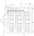
도 1은 본 발명의 실시예에 따른 터치 패널의 개략적인 평면도이다.
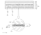
도 2는 도 1의 II-II 선을 따라서 잘라서 본 단면도이다.
도 3은 도 1에 도시한 터치 패널의 제1 센서부와 제1 배선부를 도시한 평면도이다.
도 4는 도 3의 IV-IV 선을 따라 잘라서 본 단면도이다.
도 5는 도 1에 도시한 터치 패널의 제2 센서부와 제2 배선부의 제1 부분을 도시한 평면도이다.
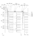
도 6은 도 1에 도시한 터치 패널의 제2 센서부와 제2 배선부의 제1 및 제2 부분을 도시한 평면도이다.
도 7은 도 6의 VII-VII 선을 따라 잘라서 본 단면도이다.
도 8은 본 발명의 실시예에 따른 터치 패널의 제1 및 제2 센서부의 다른 일 예를 도시한 평면도이다. 1 is a schematic plan view of a touch panel according to an embodiment of the present invention.
2 is a sectional view cut along the line II-II in Fig.
3 is a plan view showing the first sensor unit and the first wiring unit of the touch panel shown in FIG.
4 is a cross-sectional view taken along line IV-IV in Fig.
5 is a plan view showing a first portion of the second sensor portion and the second wiring portion of the touch panel shown in FIG.
6 is a plan view showing first and second portions of the second sensor portion and the second wiring portion of the touch panel shown in FIG.
7 is a sectional view cut along the line VII-VII in Fig.
8 is a plan view showing another example of the first and second sensor units of the touch panel according to the embodiment of the present invention.
이하에서는 첨부한 도면을 참조하여 본 발명의 실시예를 상세하게 설명한다. 그러나 본 발명이 이러한 실시예에 한정되는 것은 아니며 다양한 형태로 변형될 수 있음은 물론이다. Hereinafter, embodiments of the present invention will be described in detail with reference to the accompanying drawings. However, it is needless to say that the present invention is not limited to these embodiments and can be modified into various forms.
도면에서는 본 발명을 명확하고 간략하게 설명하기 위하여 설명과 관계 없는 부분의 도시를 생략하였으며, 명세서 전체를 통하여 동일 또는 극히 유사한 부분에 대해서는 동일한 도면 참조부호를 사용한다. 그리고 도면에서는 설명을 좀더 명확하게 하기 위하여 두께, 넓이 등을 확대 또는 축소하여 도시하였는바, 본 발명의 두께, 넓이 등은 도면에 도시된 바에 한정되지 않는다. In the drawings, the same reference numerals are used for the same or similar parts throughout the specification. In the drawings, the thickness, the width, and the like are enlarged or reduced in order to make the description more clear, and the thickness, width, etc. of the present invention are not limited to those shown in the drawings.
그리고 명세서 전체에서 어떠한 부분이 다른 부분을 "포함"한다고 할 때, 특별히 반대되는 기재가 없는 한 다른 부분을 배제하는 것이 아니며 다른 부분을 더 포함할 수 있다. 또한, 층, 막, 영역, 판 등의 부분이 다른 부분 "위에" 있다고 할 때, 이는 다른 부분 "바로 위에" 있는 경우뿐 아니라 그 중간에 다른 부분이 위치하는 경우도 포함한다. 층, 막, 영역, 판 등의 부분이 다른 부분 "바로 위에" 있다고 할 때에는 중간에 다른 부분이 위치하지 않는 것을 의미한다. Wherever certain parts of the specification are referred to as "comprising ", the description does not exclude other parts and may include other parts, unless specifically stated otherwise. Also, when a portion of a layer, film, region, plate, or the like is referred to as being "on" another portion, it also includes the case where another portion is located in the middle as well as the other portion. When a portion of a layer, film, region, plate, or the like is referred to as being "directly on" another portion, it means that no other portion is located in the middle.
이하, 첨부한 도면을 참조하여 본 발명의 실시예에 따른 터치 패널 및 이를 포함하는 표시 장치를 상세하게 설명한다. Hereinafter, a touch panel and a display device including the same according to an embodiment of the present invention will be described in detail with reference to the accompanying drawings.
도 1은 본 발명의 실시예에 따른 터치 패널의 개략적인 평면도이고, 도 2는 도 1의 II-II 선을 따라서 잘라서 본 단면도이다. 간략하고 명확한 도시를 위하여 도 1에서는 제1 하드 코팅층(114), 오버 코팅층(116), 투명 접착층(120) 및 커버 기판(130)을 도시하지 않으며, 도 1에서 연성 인쇄 회로 기판(30)과 절연층(119)은 각기 점선 및 괘선으로 표시한다. FIG. 1 is a schematic plan view of a touch panel according to an embodiment of the present invention, and FIG. 2 is a cross-sectional view cut along a line II-II in FIG. The first
도 1 및 도 2를 참조하면, 본 실시예의 터치 패널(100)에는 유효 영역(AA)과 유효 영역(AA)의 외곽에 위치하는 비유효 영역(NA)이 정의될 수 있다. 유효 영역(AA)은 제1 및 제2 전극(10, 20)의 센서부(12, 22)가 위치하여 사용자의 손, 스타일러스 펜 등의 입력 장치의 터치를 감지하는 영역이다. 비유효 영역(NA)은 유효 영역(AA)에서 감지된 정보를 전달할 수 있도록 외부(외부 회로, 예를 들어, 표시 장치에서 터치 패널(100)을 제어하는 터치 제어 유닛(도시하지 않음))에 연결되는 연성 인쇄 회로 기판(flexible printed circuit board, FPCB)(19), 이에 연결되는 제1 및 제2 전극(10, 20)의 배선부(14, 24) 등이 위치하는 영역이다. 또한, 비유효 영역(NA)에는 터치 패널(100)을 구성하는 다양한 층, 부품 등을 물리적으로 고정하며 비유효 영역(NA)에 위치한 다양한 구성을 가리는 베젤(도시하지 않음) 또는 흑색 인쇄층(도시하지 않음) 등이 위치할 수도 있다. 본 실시예에서는 전면으로 볼 때 또는 동일 평면에서 비유효 영역(NA)이 유효 영역(AA)의 외곽에 위치하는 것을 예시하였다. 그러나 본 발명이 이에 한정되는 것은 아니며 전면에서 볼 때 또는 동일 평면에서 비유효 영역(NA)이 위치하지 않는 등 다양한 변형이 가능하다. Referring to FIGS. 1 and 2, the
본 실시예에 따른 터치 패널(100)은, 제1 전극(10)과 제2 전극(20)이 함께 구비되는 전도성 필름(110)을 포함한다. 제1 전극(10)은 유효 영역(AA) 내에 위치하는 제1 센서부(12)와 비유효 영역(NA) 내에 위치하는 제1 배선부(14)를 포함할 수 있고, 제2 전극(20)은 유효 영역(AA) 내에 위치하는 제2 센서부(22)와 비유효 영역(NA) 내에 위치하는 제2 배선부(14)를 포함할 수 있다. 이때, 제1 전극(10)의 제1 센서부(12)와 제2 전극(20)의 제2 센서부(22)가 하나의 전도성 필름(110)의 일면 쪽에 함께 위치하여, 터치 패널(100)의 구조를 단순화할 수 있다. 본 실시예에서는 제1 및 제2 센서부(12, 22)를 외부 또는 연성 인쇄 회로 기판(30)과 연결하는 제1 및 제2 배선부(14, 24)의 구조를 개선하여 터치 패널(100)의 구조를 좀더 단순화한다. 이에 대해서는 추후에 좀더 상세하게 설명한다. 그리고 터치 패널(100)은 커버 기판(130)과, 커버 기판(130)과 전도성 필름(110)을 접착하는 투명 접착층(120)을 포함할 수 있다. 그러나 커버 기판(130)과 투명 접착층(120)이 필수적인 것은 아니며 이에 대한 다양한 변형이 가능하다.The
커버 기판(130)은 터치 패널(100)을 외부의 충격으로부터 보호하면서 터치 패널(100)을 통하여 광이 투과할 수 있도록 하는 물질로 구성될 수 있다. 일 예로, 커버 기판(130)은 유리, 플라스틱 등을 포함할 수 있다. 그러나 본 발명이 이에 한정되는 것은 아니며 커버 기판(130)의 물질 등은 다양한 변형이 가능하다.The
커버 기판(130)과 전도성 필름(110) 사이에 투명 접착층(120)이 위치(일 예로, 접촉)하여 이들을 접합할 수 있다. 이와 같이 단일의 투명 접착층(120)을 사용하는 것에 의하여 터치 패널(100)을 형성할 수 있으므로 터치 패널(100)의 적층 구조를 단순화할 수 있다. A transparent
투명 접착층(120)은 양쪽에 위치한 층들을 접착할 수 있는 접착 특성과 함께 투광성을 가지는 물질, 즉, 광학성 투명 접착 물질(optically clear adhesive, OCA)로 구성될 수 있다. 광학성 투명 접착 물질은 접착력이 우수하고, 제1 및/또는 제2 전극(10, 20)의 열화를 방지할 수 있도록 내습성, 내열 발포성, 가공성 등이 우수한 물질일 수 있다. 투명 접착층(120)으로는 광학성 투명 접착 물질로 알려진 다양한 물질을 사용할 수 있다.The transparent
전도성 필름(110)은, 베이스 필름(112)과, 베이스 필름(112)의 일면 쪽에서 서로 이격되어 형성되는 제1 전극(10)(특히, 제1 센서부(12)) 및 제2 전극(20)(특히, 제2 센서부(22))을 포함한다. 그리고 전도성 필름(110)은, 베이스 필름(112)과 제1 및 제2 전극(10, 20) 사이에 위치하는 제1 하드 코팅층(114)과, 적어도 유효 영역(AA)에서 베이스 필름(112)(좀더 정확하게는, 제1 하드 코팅층(114))과 제1 전극(10) 및 제2 전극(20)을 덮는 오버 코팅층(116)과, 베이스 필름(112)의 타면에 위치하는 제2 하드 코팅층(118)을 더 포함할 수 있다. The
베이스 필름(112)은 전도성 필름(110)의 기계적 강도를 유지하면서 투광성 및 절연성을 가지는 물질로 구성되는 필름, 시트 등일 수 있다. 베이스 필름(112)은 각기, 폴리에틸렌, 폴리프로필렌, 폴리에틸렌테레프탈레이트, 폴리에틸렌-2,6-나프탈레이트, 폴리프로필렌테레프탈레이트, 폴리이미드, 폴리아미드이미드, 폴리에테르설판, 폴리에테르에테르케톤, 폴리카보네이트, 폴리아릴레이트, 셀룰로오스프로피오네이트, 폴리염화비닐, 폴리염화비닐리덴, 폴리비닐알코올, 폴리에테르이미드, 폴리페닐렌설피드, 폴리페닐렌옥사이드, 폴리스티렌 등의 물질 중 적어도 하나를 포함할 수 있다. 일례로, 베이스 필름(112)이 폴리에틸렌테레프탈레이트로 구성될 수 있다. 그러나 본 발명이 이에 한정되는 것은 아니며, 베이스 필름(112)으로 상술한 물질 외의 다양한 물질이 사용될 수 있다.The
베이스 필름(112)의 일면 위에 제1 하드 코팅층(114)이 형성된다. 본 실시예에서는 베이스 필름(112)과 제1 및 제2 전극(10, 20) 사이에 제1 하드 코팅층(114)을 위치시켜, 제1 및 제2 전극(10, 20)의 다양한 특성을 향상할 수 있다. 이에 대해서는 추후에 제1 및 제2 전극(10, 20) 및 오버 코팅층(116)을 먼저 설명한 후에 상세하게 설명한다.A first
본 실시예에서 제1 센서부(12)와 제2 센서부(22)가 베이스 필름(112)의 일면 위에서(좀더 구체적으로는, 베이스 필름(112)의 일면 위에 위치한 제1 하드 코팅층(114) 위에서) 동일 평면 상에 위치할 수 있다. The
본 실시예에서 제1 센서부(12) 및 제2 센서부(22)는, 전도성 및 투광성을 가지는 투명 전도성 물질을 포함한다. 일 예로, 제1 및 제2 센서부(12, 22)가 네트워크 구조를 가지는 나노 소재의 금속 물질을 포함하는 도전체(12a)(예를 들어, 은 나노 와이어, 구리 나노 와이어, 백금 나노 와이어 등과 같은 금속 나노 와이어, 특히, 은 나노 와이어)를 포함할 수 있다. 여기서, 네트워크 구조라 함은, 나노 와이어 등과 나노 소재의 도전체가 이웃한 나노 소재의 도전체들과 서로 복수의 접촉점을 가지면서 얽혀서 불규칙한 그물 구조, 불규칙한 메쉬(mesh) 구조 등을 형성하여, 복수의 접촉점을 통하여 전기적인 연결이 이루어지는 구조라 할 수 있다. In this embodiment, the
네트워크 구조를 형성하는 나노 소재의 도전체(12a)를 포함하는 제1 및 제2 센서부(12, 22)는, 균일한 두께의 층 내부에 나노 소재의 도전체(12a)가 위치하거나, 나노 소재의 도전체(12a) 사이에 빈 공간을 가지는 상태로 형성될 수도 있다. 실제로 제1 및 제2 센서부(12, 22)는 아주 적은 양의 용매, 바인더 등에 나노 소재의 도전체(12a)를 혼합한 혼합물을 도포하여 형성된다. 이에 따라 제1 및 제2 센서부(12, 22)는, 용매, 바인더 등이 잔류하여 형성된 잔류 부분(12b)이 상대적으로 작은 제1 두께(T1)를 가지면서 형성되고, 도전체(12a)가 잔류 부분(12b)의 외부까지 연장된다. 이에 따라 도전체(12a)에 의하여 형성된 네트워크 구조가 상대적으로 두꺼운 제2 두께(T2)를 가지면서 형성될 수도 있다. 이하에서 제1 또는 제2 센서부(22)의 두께는 잔류 부분(12b)의 두께인 제1 두께(T1)을 의미하는 것이 아니라 잔류 부분(12b)과 함께 잔류 부분(12b) 위로 돌출된 도전체(12a)가 위치한 층의 전체 두께, 즉 제2 두께(T2)를 기준으로 한다. The first and
이와 같이 제1 및 제2 센서부(12, 22)가 투명 전도성 물질인 나노 소재의 도전체(12a)를 포함하면, 증착 방법보다 공정 비용이 저렴한 습식 코팅 방법에 의하여 제1 및 제2 센서부(12, 22)가 형성될 수 있다. 즉, 나노 와이어 등으로 구성된 나노 소재의 도전체를 포함하는 페이스트, 잉크, 혼합물, 용액 등을 도포하는 습식 코팅법에 의하여 전극층을 형성한 다음 패터닝하는 것에 의하여 제1 및 제2 센서부(12, 22)을 형성할 수 있다. 이때, 습식 코팅 시 사용되는 용액, 혼합물 또는 페이스트 등에서 나노 소재의 도전체(12a)의 농도가 매우 낮다(일례로, 1% 이하). 이에 따라 제1 및 제2 센서부(12, 22)의 형성에 필요한 비용을 절감할 수 있어 생산성을 향상할 수 있다.When the first and
그리고 제1 및 제2 센서부(12, 22)가 나노 소재의 도전체(12a)를 포함하면, 광을 투과할 수 있는 특성을 가지면서도 낮은 저항 및 우수한 전기적 특성을 가지게 된다. 일례로, 은(Ag)의 나노 입자 표면은 여러 가지 결정면을 가지므로 이에 의하여 쉽게 이등방성 성장을 유도할 수 있으므로, 이에 의하여 쉽게 은 나노 와이어를 제조할 수 있다. 은 나노 와이어는 저항이 대략 10 Ω/□ 내지 400 Ω/□의 값을 가져, 낮은 저항(예를 들어, 10 Ω/□ 내지 150 Ω/□)을 구현할 수 있다. 이에 따라 다양한 저항을 가지는 제1 및 제2 센서부(12, 22)을 형성할 수 있다. 특히, 대략 200 Ω/□ 내지 400 Ω/□의 저항을 가지는 인듐 틴 산화물보다 우수한 전기 전도도를 가지는 제1 및 제2 센서부(12, 22)을 형성할 수 있다. 그리고 은 나노 와이어는 투과율이 인듐 틴 산화물보다 우수하여, 일례로 90% 이상의 투과율을 가질 수 있다. 또한, 플렉서블한 특성을 가지므로 플렉서블한 장치에도 적용될 수 있으며, 재료 수급이 안정적이다. When the first and
상술한 바와 같은 나노 와이어(특히, 은 나노 와이어)는, 일례로, 반경이 10nm 내지 60nm이고, 장축이 10㎛ 내지 200㎛ 수 있다. 이러한 범위에서 우수한 종횡비(aspect ratio)(일례로, 1:300~1:20000)를 가져 네트워크 구조를 잘 형성할 수 있고 제1 및 제2 센서부(12, 22)가 잘 보이지 않도록 할 수 있다. 그러나 본 발명이 이에 한정되는 것은 아니며 나노 와이어의 반경, 장축, 종횡비는 다양한 값을 가질 수 있다. The nanowire (particularly, silver nanowire) as described above may have a radius of 10 nm to 60 nm and a major axis of 10 mu m to 200 mu m, for example. It is possible to form the network structure well and to prevent the first and
제1 및 제2 센서부(12, 22)의 두께는 터치 패널(100)의 크기, 요구되는 저항 값, 제1 및 제2 센서부(12, 22)의 물질에 따라 다양하게 변화될 수 있다. 이때, 제1 및 제2 센서부(12, 22)가 네트워크 구조를 가지는 금속 나노 와이어를 포함하면 두께를 최소화할 수 있는데, 일 예로, 제1 및 제2 센서부(12, 22)가 50nm 내지 350nm의 두께를 가질 수 있다. 이러한 두께에서 원하는 저항을 가지는 제1 및 제2 센서부(12, 22)를 형성하기 쉽기 때문이다. 그러나 본 발명이 이에 한정되는 것은 아니며 제1 및 제2 센서부(12, 22)의 두께는 다양한 값을 가질 수 있다. The thicknesses of the first and
이와 같이 본 실시예에서는 제1 및 제2 센서부(12, 22)가 네트워크 구조를 형성하는 나노 소재의 도전체(12a)를 포함하여, 재료 비용을 절감하고 다양한 특성을 향상할 수 있다. As described above, in this embodiment, the first and
그리고 비유효 영역(NA)에서 제1 센서부(12)에 연결되는 제1 배선부(14)가 연결되고, 제2 센서부(22)에 연결되는 제2 배선부(24)가 연결된다. 제1 및 제2 배선부(14, 24)에는 연성 인쇄 회로 기판(30)이 연결 또는 부착될 수 있다. 본 실시예에서는 제1 및 제2 배선부(14, 24)가 함께 하나의 연성 인쇄 회로 기판(30)에 연결될 수 있다. 이는 제1 및 제2 센서부(12, 22)가 전도성 필름(110)에서 동일한 일면 쪽에(즉, 베이스 필름(112)의 일면 위에, 좀더 구체적으로 제1 하드 코팅층(114) 위에) 위치하였기 때문이다. The
제1 센서부(12) 및 제1 배선부(14)를 포함하는 제1 전극(10), 그리고 제2 센서부(22) 및 제2 배선부(24)를 포함하는 제2 전극(20)의 구조 또는 형상에 대해서는 추후에 상세하게 설명한다.A
제1 및 제2 배선부(14, 24)에는 외부와의 연결을 위한 연성 인쇄 회로 기판(30)이 연결될 수 있다. 연성 인쇄 회로 기판(30)은, 베이스 부재와, 베이스 부재 위에 형성되는 배선부를 포함할 수 있다. 연성 인쇄 회로 기판(30)의 배선부와 제1 및 제2 배선부(14, 24)를 서로 접촉시키는 것에 의하여 제1 및 제2 배선부(14, 24)와 연성 인쇄 회로 기판(30)을 전기적으로 연결할 수 있다. 그러나 본 발명이 이에 한정되는 것은 아니며, 연성 인쇄 회로 기판(30)의 배선부와 제1 및 제2 배선부(14, 24) 사이에 비등방성 전도성 접착체(anisotropic conductive adhesive, ACA), 비등방성 전도성 페이스트(anisotropic conductive paste, ACP), 비등방성 전도성 필름(anisotropic conductive film, ACF) 등의 전도성 접착 부재(도시하지 않음)을 위치하여 이들을 전기적으로 연결할 수도 있다. The first and
도면에서는 제1 및 제2 배선부(14, 24)와 이에 연결되는 연성 인쇄 회로 기판(30)이 유효 영역(AA)의 일측에 위치하는 것을 예시하였다. 그러나 본 발명이 이에 한정되는 것은 아니며 제1 및 제2 배선부(14, 24) 및 연성 인쇄 회로 기판(30)이 다양한 배치를 가질 수 있다. In the drawing, the first and
베이스 필름(112)의 일면 위에서 베이스 필름(112), 그리고 제1 및 제2 센서부(12, 22)를 덮는 오버 코팅층(116)은 제1 및 제2 센서부(12, 22)를 물리적 및 화학적으로 보호한다. 좀더 구체적으로, 오버 코팅층(116)은 잔류 부분(12b) 외부까지 연장된 도전체(12a)의 외면을 감싸면서 전체적으로 덮어 도전체(12a)가 손상되거나 도전체(12a)가 산화되는 것을 방지할 수 있다. 좀더 상세하게는, 잔류 부분(12b) 위로 노출된 도전체(12a)가 외부의 힘 등에 의하여 꺽이는 것과 같이 물리적으로 손상되는 것을 방지할 수 있다. 또한, 도전체(12a)는 외부의 대기에 오랜 시간 노출될 경우에 산화되어 전기 전도성이 저하될 수 있으므로, 오버 코팅층(116)이 이를 방지할 수 있도록 도전체(12a)를 덮으면서 형성될 수 있다. 본 실시예에서는 제1 및 제2 센서부(12, 22)가 네트워크 구조를 형성하는 나노 소재의 도전체(12a)를 포함하기 때문에, 도전체(12a)의 물리적 안정성을 향상하고 산화를 방지할 수 있는 오버 코팅층(116)을 형성한 것이다. 일 예로, 오버 코팅층(116)의 일부는 도전체(12a) 사이의 공간으로 함침되어 도전체(12a) 사이의 공간을 메우면서 위치하고, 다른 일부는 도전체(12a)의 위로 형성될 수 있다. 본 실시예에서와 달리, 도전체(12a)가 잔류 부분(12b) 위로 돌출되지 않고 잔류 부분(12b)의 내부에 위치한 경우에도 오버 코팅층(116)이 잔류 부분(12b)의 내부로 침입한 대기 등에 의하여 도전체(12a)가 산화되는 것을 방지할 수 있다. 이를 위하여 오버 코팅층(116)은 제1 및 제2 센서부(12, 22) 또는 도전체(12a)에 직접 접촉하도록 형성될 수 있다. The
오버 코팅층(116)은 베이스 필름(112) 위에서 제1 및 제2 센서부(12, 22)를 덮으면서 적어도 유효 영역(AA)에 전체적으로 형성될 수 있다. 여기서, 전체적으로 형성되었다고 함은 빈틈 없이 완벽하게 형성된 경우뿐만 아니라 불가피하게 일부 부분이 형성되지 않은 경우를 포함할 수 있다. The
이러한 오버 코팅층(116)는 수지로 구성될 수 있다. 일례로, 오버 코팅층(116)은 아크릴 레진으로 이루어질 수 있으나, 본 발명이 이에 한정되는 것은 아니며 오버 코팅층(116)이 다른 물질을 포함할 수 있다. 그리고 오버 코팅층(116)은 다양한 코팅 방법에 의하여 제1 및 제2 센서부(12, 22)를 전체적으로 덮도록 형성될 수 있다. The
일례로, 오버 코팅층(116)의 두께가 5nm 내지 50nm일 수 있다. 오버 코팅층(116)의 두께가 5nm 미만이면 도전체(12a)의 산화를 방지하는 효과가 충분하지 않을 수 있다. 그리고 오버 코팅층(116)의 두께가 50nm를 초과하면, 재료의 비용이 증가할 수 있다. 그러나 본 발명이 이에 한정되는 것은 아니며 오버 코팅층(116)의 두께는 다양한 값을 가질 수 있다. In one example, the thickness of the
도면 및 상술한 실시예에서는 제1 및 제2 센서부(12, 22)의 잔류 부분(12b)과 오버 코팅층(116)이 서로 다른 층으로 구성된 것을 예시로 하였다. 그러나 본 발명이 이에 한정되는 것은 아니다. 다른 실시예로, 상술한 제1 및 제2 센서부(12, 22)의 도전체(12a) 및 잔류 부분(12b)과 오버 코팅층(116)을 구성하는 물질을 함께 혼합한 잉크 등을 도포하는 것에 의하여, 단일의 층인 오버 코팅층(116) 내부에 도전체(12a)가 위치하는 것도 가능하다. 이 외에도 다양한 변형이 가능함은 물론이다. In the drawings and the above-described embodiments, it is exemplified that the residual portion 12b of the first and
베이스 필름(112)와 제1 및 제2 전극(10, 20) 사이에 위치한 제1 하드 코팅층(114)을 다시 설명한다. 상술한 바와 같이 본 실시예에서는 제1 및 제2 센서부(12, 22)의 도전체(12a)가 네트워크 구조를 가지는 나노 소재로 구성되므로, 전도성 필름(110) 또는 이를 형성하기 위한 구조체가 코팅을 위한 주행 중에 외력에 의하여 쉽게 손상될 수 있다. 즉, 본 실시예와 같은 전도성 필름(110)에서는 작은 외력이 인가되어도 네트워크 구조를 형성하는 나노 소재(예를 들어, 나노 와이어) 사이의 컨택 특성에 영향을 주기 때문에 제1 및 제2 센서부(12, 22)의 전기 전도도가 변화할 수 있다. 이에 따라 본 실시예에서는 베이스 필름(112)과 제1 전극(10)(특히, 제1 및 제2 센서부(12, 22)) 사이에 상대적으로 높은 경도를 가지는(즉, 제1 전극(10) 및 오버 코팅층(116))보다 높은 경도를 가지는) 제1 하드 코팅층(114)을 위치시켜 전도성 필름(110)의 전체적인 경도를 높일 수 있다. 이에 의하여 전도성 필름(110)에 외력이 가해지더라도 제1 및 제2 센서부(12, 22) 내의 도전체(12a)의 컨택 특성이 높은 상태로 유지될 수 있도록 한다. The first
그리고 베이스 필름(112)의 상면은 상대적으로 큰 표면 거칠기를 가지면서 울퉁불퉁하게 형성된다. 이러한 베이스 필름(112)의 울퉁불퉁한 표면에 의하여 난반사가 증가할 수 있다. 이때, 본 실시예와 같이 네트워크 구조의 도전체(12a)가 적용되는 경우에는 네트워크 구조 등에 의하여 난반사 발생이 심화될 수 있어, 헤이즈(탁도)가 상승하고 투과율이 저하될 수 있다. 또한, 상술한 베이스 필름(112)의 거친 표면에 제1 및 제2 센서부(12, 22)를 형성하게 되면 네트워크 구조를 가지는 나노 소재를 포함하는 제1 및 제2 센서부(12, 22)을 균일한 두께로 형성하기 어렵다. 이에 따라 코팅되지 않은 영역이 발생하고 제1 및 제2 센서부(12, 22)에서 면저항 편차가 증가할 수 있다.And the upper surface of the
이를 고려하여 본 실시예에서는 베이스 필름(112) 위에 제1 하드 코팅층(114)을 전체적으로 도포하여 상면을 평탄화한다. 즉, 제1 하드 코팅층(114)의 상면이 베이스 필름(112)의 상면(또는 제1 하드 코팅층(114))의 하면보다 작은 표면 거칠기를 가질 수 있다. 이와 같이 제1 하드 코팅층(114)에 의하여 표면이 평탄화되면 헤이즈 및 난반사를 최소화하고 투과율을 최대화할 수 있다. 이에 의하여 전도성 필름(110)의 광특성을 향상할 수 있다. 또한, 제1 및 제2 전극(10, 20)(예를 들어, 제1 및 제2 센서부(12, 22))의 코팅 특성을 개선할 수 있다. 이에 따라 제1 및 제2 센서부(12, 22)의 면 저항, 광 특성 등의 다양한 특성의 편차를 최소화할 수 있다. In consideration of this, in the present embodiment, the first
이러한 제1 하드 코팅층(114)은 경도를 증가시킬 수 있고 제1 및 제2 센서부(12, 22)의 코팅 특성을 개선할 수 있는 다양한 물질을 포함할 수 있다. 일례로, 제1 하드 코팅층(114)은, 우레탄계 수지, 멜라민계 수지, 알키드계 수지, 에폭시계 수지, 아크릴계 수지, 폴리에스테르계 수지, 폴리비닐알코올계 수지, 염화 비닐계 수지, 염화 비닐리덴계 수지, 폴리 알릴레이트계 수지, 술폰계 수지, 아미드계 수지, 이미드계 수지, 폴리에테르술폰계 수지, 폴리에테르이미드계 수지, 폴리카보네이트계 수지, 실리콘계 수지, 불소계 수지, 폴리올레핀계 수지, 스티렌계 수지, 비닐피롤리돈계 수지, 셀룰로오스계 수지, 아크릴로니트릴계 수지 등의 물질 중 적어도 하나를 포함할 수 있다. 특히, 본 실시예에서 제1 하드 코팅층(114)은 아크릴계 수지를 포함할 수 있다. 그러나 본 발명이 이에 한정되는 것은 아니며 제1 하드 코팅층(114)이 이러한 물질 외의 다양한 물질로 구성될 수도 있다. The first
제1 하드 코팅층(114)은 1H 내지 5H의 연필 경도를 가질 수 있다. 제1 하드 코팅층(114)의 연필 경도가 1H 미만이면 상술한 효과를 충분하게 가지지 힘들 수 있고, 연필 경도가 5H를 초과하는 제1 하드 코팅층(114)은 제조가 어려울 수 있다. 그리고 제1 하드 코팅층(114)은 물과의 접촉각이 40도 내지 60도일 수 있고, 표면 장력이 20 dyne/cm 내지 50 dyne/cm일 수 있다. 이러한 제1 하드 코팅층(114)의 접촉각 및 표면 장력은 다른 층(예를 들어, 베이스 필름(112) 또는 베이스 필름(112)과 제1 하드 코팅층(114) 사이에 위치하는 프라이머층(도시하지 않음))의 접촉각 및 표면 장력보다 낮은 수치를 가진다. 이에 의하여 제1 하드 코팅층(114) 상에 제1 및 제2 센서부(12, 22)를 형성할 때 제1 및 제2 센서부(12, 22)가 쉽게 형성될 수 있다. The first
이러한 제1 하드 코팅층(114)은 전도성 필름(110)의 경도를 높이면서 표면을 평탄화할 수 있는 정도의 두께를 가질 수 있다. 이를 위하여 제1 하드 코팅층(114)은 제1 및 제2 센서부(12, 22) 및 오버 코팅층(116)보다 두꺼운 두께를 가질 수 있다. 그러나 두께가 너무 두꺼워질 경우에 전도성 필름(110)의 두께가 불필요하게 증가할 수 있으므로, 제1 하드 코팅층(114)은 베이스 필름(112)의 두께보다는 얇은 두께를 가질 수 있다. The first
예를 들어, 제1 하드 코팅층(114)의 두께는 1㎛ 내지 10㎛일 수 있다. 제1 하드 코팅층(114)의 1㎛ 미만이면 상술한 제1 하드 코팅층(114)의 효과를 충분히 기대하기 어려울 수 있고, 두께가 10㎛를 초과하면 재료 사용에 의한 비용이 증가하고 박형화가 어려울 수 있다. 제1 하드 코팅층(114)의 효과, 박형화 등을 충분히 고려하면 제1 하드 코팅층(114)의 두께가 3㎛ 내지 5㎛일 수 있다. 그러나 본 발명이 이에 한정되는 것은 아니며 제1 하드 코팅층(114)이 다른 두께를 가질 수도 있다. For example, the thickness of the first
한편, 베이스 필름(112)의 타면 위에는 제2 하드 코팅층(118)이 더 위치할 수 있다. 제2 하드 코팅층(118)은 공정 중에 발생할 수 있는 손상(일례로, 스크래치) 등으로부터 전도성 필름(110)을 보호하기 위한 층이다. 제2 하드 코팅층(118)의 물질, 두께 등의 다양한 특성은 제1 하드 코팅층(114)과 동일 또는 극히 유사할 수 있으므로, 상세한 설명을 생략한다. 이와 같이 제1 및 제2 하드 코팅층(118)을 함께 구비하여 본 실시예에 따른 전도성 필름(110)은 2H 이상(예를 들어, 2H 내지 10H)의 연필 경도를 가질 수 있다. 그러나 본 발명이 이에 한정되는 것은 아니며 제2 하드 코팅층(118)이 구비되지 않는 것도 가능하다. On the other hand, the second
도면에서는 제1 및 제2 전극(10, 20)이 형성된 전도성 필름(110)의 일면이 커버 기판(130)에 대향하도록 위치한 것을 예시하였다. 그러면 커버 기판(130)과 제2 하드 코팅층(118)이 터치 패널(100)의 양쪽 외면을 구성하여 외부 충격으로부터 터치 패널(100)을 보호할 수 있다. 그러나 본 발명이 이에 한정되는 것은 아니며 제1 및 제2 전극(10, 20)이 형성된 전도성 필름(110)의 일면이 외부 면 쪽에 위치하는 것도 가능하다. In the drawing, one surface of the
본 실시예에서는 제1 전극(10)의 제1 센서부(12)와 제2 전극(20)의 제2 센서부(22)가 동일 평면 상에서 서로 교차하지 않고(또는 평면상에서 서로 중첩되지 않고) 서로 상보적인 형상을 가지도록 형성된다. 즉, 제1 센서부(12)와 제2 센서부(22)가 일정 거리를 두고 서로 이격되어 위치하며 서로 반대되는 형상을 가질 수 있다. 예를 들어, 제1 센서부(12)가 오목부를 구비한 부분에서는 제2 센서부(22)가 돌출부를 구비하여 오목부와 돌출부가 균일한 거리를 두고 이격하도록 형성될 수 있다. 이러한 제1 및 제2 센서부(12, 22)는 동일한 공정에서 함께 형성되어 동일한 도전체(12a)를 구비할 수 있다. 이러한 구조의 제1 및 제2 센서부(12, 22)에 적합하도록 제1 및 제2 배선부(14, 24)가 개선된 구조를 가지며 제1 및 제2 배선부(14, 24)가 위치한 부분에 부분적으로 절연층(119)이 구비될 수 있다. 이를 도 1과 함께 도 3 내지 도 8을 참조하여 상세하게 설명한다. The
먼저, 도 1, 도 3 및 도 4를 참조하여 제1 전극(10)을 상세하게 설명한다.First, the
도 3은 도 1에 도시한 터치 패널(100)의 제1 센서부(12)와 제1 배선부(14)를 도시한 평면도이고, 도 4는 도 3의 IV-IV 선을 따라 잘라서 본 단면도이다. 간략하고 명확한 도시를 위하여 도 3에는 제1 하드 코팅층(114), 오버 코팅층(116), 제2 전극(20), 절연층(119), 투명 접착층(120) 및 커버 기판(130)을 도시하지 않는다. 그리고 도 3에서 연성 인쇄 회로 기판(30)은 점선으로 표시한다. 3 is a plan view showing the
도 1, 도 3 및 도 4를 참조하면, 복수의 제1 센서부(12)가 제1 방향(도면의 x축 방향)으로 서로 이격되어 배치되며 각각의 제1 센서부(12)는 제1 방향과 교차하는 제2 방향(도면의 y축 방향)으로 길게 연장된다. 그리고 제1 배선부(14)는 복수의 제1 센서부(12)에 대응하여 복수의 제1 센서부(14)에 각기 연결되도록 복수 개 구비된다. 일 예로, 제1 배선부(14)는 제1 센서부(12)에 일대일 대응할 수 있다. 1, 3, and 4, a plurality of
제1 센서부(12)는 제2 방향에서 하나의 센서 부분(121)을 구비할 수 있다. 제1 센서부(12)의 센서 부분(121)의 형상은 제2 센서부(22)의 센서 부분(221, 222, 223)과 상보적인 결합을 하여 서로 충분한 면적으로 마주보는 다양한 형상을 가질 수 있다. The
도면에서는, 일 예로, 제1 센서부(12)의 센서 부분(121)이, 하나의 줄기부(121a)와, 하나의 줄기부(121a)로부터 일 방향으로 돌출되는 복수의 가지부(121b)를 포함하는 것을 예시하였다. 그리고, 도 5에 도시한 바와 같이, 제2 센서부(22)의 센서 부분(221, 222, 223)이 하나의 줄기부(221a)와, 하나의 줄기부(221a)로부터 제1 센서부(12)의 두 개의 줄기부(121b) 사이로 돌출되는 복수의 가지부(221b)를 포함하는 것을 예시하였다. 이와 같은 형상을 가지면 제1 센서부(12)의 하나의 센서 부분(121)과 제2 센서부(22)의 복수의 센서 부분(221, 222, 223)이 서로 상보적인 형상을 가지면서 넓은 면적으로 마주보며 형성될 수 있다. 이에 의하여 터치 감도를 향상할 수 있다. The
그러나 본 발명이 이에 한정되는 것은 아니며 제1 센서부(12)의 센서 부분(121)의 형상, 제2 센서부(22)의 센서 부분(221, 222, 223)의 형상 등은 다양하게 변형될 수 있다. 제1 센서부(12) 및 제2 센서부(22)의 형상의 다른 일 예를 도 8을 참조하여 설명한다. 도 8은 본 발명의 실시예에 따른 터치 패널의 제1 및 제2 센서부(12, 22)의 다른 일 예를 도시한 평면도이다. 명확하고 간략한 도시를 위하여 도 8에서는 하나의 제1 센서부(12)와 하나의 제2 센서부(22)만을 도시하였다. However, the present invention is not limited thereto, and the shape of the
도 8을 참조하면, 제2 센서부(22)의 센서 부분(221, 222, 223)이 하나의 줄기부(221a)와 이를 가로질러 양쪽으로 돌출되는 복수의 가지부(221b)를 구비할 수 있다. 이때, 제1 센서부(12)는 전체적으로 사각형의 형상을 가지면서 센서 부분(221, 222, 223)에 대응하며 센서 부분(221, 222, 223) 및 내부 배선(226a, 226b, 226c)보다 약간 큰 크기를 가지는 개구부를 구비하는 형상을 가질 수 있다. 그 외의 다양한 형상의 제1 및 제2 센서부(12, 22)가 적용될 수 있다. 8, the
다시 도 1, 도 3 및 도 4를 참조하면, 제1 센서부(12) 각각은 하나의 센서 부분(121)로부터 비유효 영역(NA)에 위치한 제1 배선부(14)까지 연장되는 연장 배선(124)을 더 포함할 수 있다. 일 예로, 연장 배선(124)은 각 제1 센서부(12)의 하나의 센서 부분(121)에 하나씩 대응되어 제1 센서부(12) 또는 센서 부분(121)에 일대일 대응할 수 있다.Referring again to FIGS. 1, 3 and 4, each of the
본 실시예에서 제1 센서부(12)에 연결되는 제1 배선부(14)의 부분에 오버 코팅층(116)이 없거나 도 4에 도시한 바와 같이 해당 부분의 오버 코팅층(116)이 제거되어 제1 센서부(12)가 노출된 부분(일 예로, 제1 센서부(12)의 단부 또는 연장 배선(124)) 위에 위치할 수 있다. 이때, 제1 배선부(14)는 제1 센서부(12)에 접촉하여 형성될 수 있다. 제1 센서부(12)를 패터닝하는 공정에서 제1 배선부(14)가 위치할 부분에 위치하는 얇은 두께의 오버 코팅층(116)이 쉽게 제거될 수 있다. 또는, 제1 배선부(14)를 형성하기 위한 금속 페이스트(예를 들어, 은 페이스트)를 도포한 이후에 이를 소성하는 공정에서 얇은 두께를 가지는 오버 코팅층(116)이 자연스럽게 제거될 수 있다. 그러나 본 발명이 이에 한정되는 것은 아니다. 따라서 오버 코팅층(116)을 다른 패터닝 공정 등에 의하여 제거할 수도 있다. 그리고 제1 센서부(12)에 연결되는 제1 배선부(14)의 부분이 제1 센서부(12)와 동일 평면 상에 위치하여 제1 배선부(14)의 해당 부분과 제1 센서부(12)의 측면이 서로 접촉할 수도 있다. 또는, 제1 배선부(14)가 오버 코팅층(116)을 사이에 두고 제1 센서부(12) 위에 위치하는 것에 의하여 제1 배선부(14)와 제1 센서부(12)가 전기적으로 연결될 수도 있다. 그 외의 다양한 변형이 가능하다. In this embodiment, the
좀더 구체적으로, 제1 배선부(14)는 제1 센서부(12)로부터 연장되는 배선(142)과, 배선(142)에 연결되며 연성 인쇄 회로 기판(30)에 연결되는 부분인 패드(144)를 포함할 수 있다. 배선(142)은 상대적으로 얇은 폭으로 형성되어 비유효 영역(NA)의 크기를 최소화할 수 있고, 패드(144)는 배선(142)보다 넓은 폭을 가져 연성 인쇄 회로 기판(30)과의 연결 특성을 향상할 수 있다. 이때, 제1 배선부(14)는, 제1 센서부(12)와 동일 평면 상에 위치하는 부분을 포함할 수 있다. 본 실시예에서는 제1 배선부(14)의 배선(142)의 적어도 일부와 패드(144)가 제1 센서부(12)와 동일 평면 상에 위치한다. 이에 의하여 간단한 구조에 의하여 안정적으로 제1 배선부(14)를 제1 센서부(12)에 연결할 수 있다. 그러나 본 발명이 이에 한정되는 것은 아니며 제1 배선부(14)가 다양한 형상을 가지거나 다양한 위치에 형성될 수 있다. More specifically, the
제1 배선부(14)는 제1 센서부(12)와 다른 물질 또는 구조 등을 가질 수 있다. 좀더 구체적으로, 제1 배선부(14)는 서로 접촉하여 밀집되는 금속 입자들이 전체적으로 위치하여 제1 센서부(12)보다 충진 밀도가 높을 수 있다. 이와 같이 제1 배선부(14)는 조밀하게 채워지는 금속을 주성분(가장 많이 포함되는 물질, 또는 50 중량부 이상으로 포함되는 물질)으로 할 수 있으며, 일 예로, 은(Ag)을 주성분으로 할 수 있다. 그러나 본 발명이 이에 한정되는 것은 아니며 제1 배선부(14)가 다양한 전도성 물질을 포함할 수 있다. 예를 들어, 본 실시예에서는 제1 센서부(12)와 제1 배선부(14)가 서로 다른 구조를 가지는 예시하였으나, 제1 배선부(14)가 제1 센서부(12)와 동일한 물질로 구성되는 일체의 구조로 형성될 수도 있다. 이 경우에는 제1 배선부(14)가 제1 센서부(12)와 같은 나노 소재의 도전체(12a)를 포함할 수 있다. 그러면, 제1 센서부(12) 및 제1 배선부(14)를 형성하는 제조 공정을 단순화할 수 있다. 이 경우에는 제1 배선부(14)가 전체적으로 제1 센서부(12)와 동일 평면 상에서 위치하며, 오버 코팅층(116)이 제1 센서부(12) 및 제1 배선부(14)를 모두 덮으면서 형성될 수 있다.The
제1 배선부(14)는 다양한 방법에 의하여 형성될 수 있다. 일 예로, 제1 선부(14)는 금속 페이스트(예를 들어, 은 페이스트)를 도포(일 예로, 인쇄)한 이후에 이를 소성하여 형성될 수 있다. 제1 배선부(14)는 패턴을 가지는 상태로 도포되어 형성될 수도 있고, 또는 전체적으로 도포된 후에 감광, 현상, 에칭 공정 등을 수행하여 패터닝되어 형성될 수도 있다. 이러한 방법에 의하면 원하는 패턴의 제1 배선부(14)를 쉽게 제조할 수 있다. 그러나 본 발명이 이러한 제1 배선부(14)의 제조 방법에 한정되는 것은 아니다. The
그리고 도 1, 그리고 도 5 내지 도 7을 참조하여 제2 전극(20)을 상세하게 설명한다. The
도 5는 도 1에 도시한 터치 패널(100)의 제2 센서부(22)와 제2 배선부(24)의 제1 부분(24a)을 도시한 평면도이고, 도 6은 도 1에 도시한 터치 패널(100)의 제2 센서부(22)와 제2 배선부(24)의 제1 및 제2 부분(24a, 24b)을 도시한 평면도이다. 도 7은 도 6의 VII-VII 선을 따라 잘라서 본 단면도이다. 간략하고 명확한 도시를 위하여 도 5에는 제1 하드 코팅층(114), 오버 코팅층(116), 제1 전극(10), 제2 배선부(24)의 제2 부분(24b), 절연층(119), 투명 접착층(120) 및 커버 기판(130)을 도시하지 않고 도 6에서는 제1 하드 코팅층(114), 오버 코팅층(116), 제1 전극(10), 투명 접착층(120) 및 커버 기판(130)을 도시하지 않는다. 그리고 도 5 및 도 6에서 연성 인쇄 회로 기판(30)과 절연층(119)은 각기 점선 및 괘선으로 표시한다.5 is a plan view showing a
도 1, 도 5 내지 도 7을 참조하면, 제1 센서부(12)의 센서 부분(121)에 인접하여 이와 상보적인 형상을 가지는 센서 부분(221, 222, 223)을 포함하는 제2 센서부(22)가 구비된다. 이때, 제1 센서부(12)와 제2 센서부(22)가 서로 일대일로 대응하여 위치할 수 있고, 복수의 제2 센서부(22)가 제1 방향(도면의 x축 방향)에서 서로 이격되어 배치될 수 있다. 그리고 각각의 제2 센서부(22)는 제1 센서부(12)와 달리 제2 방향으로 하나로 길게 연장되지 않고 제2 방향에서 서로 이격되는 복수의 센서 부분(221, 222, 223)을 포함한다. Referring to FIGS. 1 and 5 to 7, a
좀더 구체적으로, 복수의 센서 부분(221, 222, 223)은 제2 방향에서 제1 위치에 위치하는 제1 센서 부분(221)과, 제2 방향에서 제1 위치와 다른 제2 위치에 위치하는 제2 센서 부분(222)을 포함한다. 도면에서는 제1 및 제2 위치와 다른 제3 위치에 제3 센서 부분(223)을 더 포함하는 것을 예시하였다. 명세서에서 전체적으로 복수의 센서 부분(221, 222, 223)이 3개의 센서 부분, 즉 제1 내지 제3 센서 부분(221, 222, 223)을 구비하는 것을 예시로 하여 설명하였다. 이는 명확한 설명을 위한 것일 뿐 본 발명이 이에 한정되는 것은 아니다. 따라서 제2 센서부(22)가 제2 방향에서 서로 다른 위치에 형성되며 서로 이격되는 두 개 이상의 센서 부분(221, 222, 223)을 가지면 족하다. More specifically, the plurality of
이때, 복수의 제2 센서부(22)에 위치하며 제2 방향에서 동일한 위치에 위치하는 센서 부분(221, 222, 223)이 각기 센서군(22a, 22b, 22c)을 형성할 수 있다. 예를 들어, 복수의 제2 센서부(22)에서 제1 위치에 위치하는 복수의 제1 센서 부분(221)이 제1 센서군(22a)을 형성하고, 복수의 제2 센서부(22)에서 제2 위치에 위치하는 복수의 제2 센서 부분(222)이 제2 센서군(22b)을 형성하고, 복수의 제2 센서부(22)에서 제3 위치에 위치하는 복수의 제3 센서 부분(222)이 제3 센서군(22c)을 형성할 수 있다. 이러한 센서군(22a, 22b, 22c)을 각기 형성하는 복수의 센서 부분(221)(222)(223)은 제2 배선부(24)에 의하여 전기적으로 연결되어 하나의 전극과 같이 기능하게 된다. 이에 따라 제2 방향으로 연장되는 제1 전극(10)의 제1 센서부(12)에 교차하는 제1 방향으로 제2 전극(20)의 복수의 센서군(22a, 22b, 22c)이 형성된다. 이에 의하여 서로 교차하도록 배치되는 제1 센서부(12)와 센서군(22a, 22b, 22c)에 의하여 터치가 이루어지는 영역을 감지할 수 있다. At this time, the
각 센서 부분(221, 222, 223)의 형상의 일 예를 이미 설명하였으므로 상세한 설명을 생략한다. 제2 센서부(22)의 복수의 센서 부분(221, 222, 223)의 형상은 특정한 형상으로 한정되는 것이 아니며 제1 센서부(12)의 센서 부분(121)의 형상과 상보적이면 족하다. Since one example of the shape of each of the
각 제2 센서부(22)는 복수의 센서 부분(221, 222, 223)에 각기 일대일 대응하여 복수의 센서 부분(221, 222, 223)으로부터 비유효 영역(NA)에 위치한 제2 배선부(24)까지 연장되는 연장 배선(226a, 226b, 226c)를 더 포함할 수 있다. 연장 배선(226a, 226b, 226c)은 각 제2 센서부(22)의 일측으로부터 연장되어 서로 일정한 간격을 두고 서로 위치할 수 있다. 터치 패널(100) 전체에서 연장 배선(226a, 226b, 226c)은 복수의 제2 센서부(22)에 포함되는 모든 센서 부분(221, 222, 223)의 총 개수와 동일한 개수만큼 형성될 수 있다. Each of the
제2 배선부(24)는, 제2 센서부(22)와 동일 평면 상에 위치하는 제1 부분(24a)과 제2 센서부(22)와 다른 층에 위치하는 제2 부분(24b)을 포함할 수 있다. 즉, 제1 부분(24a)은 베이스 필름(112)의 일면 위(좀더 정확하게는, 제1 하드 코팅층(114) 위)에서 제2 센서부(22)와 나란히 위치하는 부분을 포함할 수 있다. 그리고 제2 부분(24b)은 절연층(119)을 사이에 두고 제2 센서부(22) 또는 제1 부분(24a)과 이격되되, 컨택홀(119a)에서는 제1 부분(24a)과 연결될 수 있다. The
본 실시예에서는 제2 배선부(24)가, 제2 센서부(22)에 전기적으로 연결(일 예로, 접촉)되는 연장 부분(242)과, 제2 방향에서 서로 대응하는 위치에 위치하는 복수의 센서 부분(221, 222, 222)을 연결하는 연결 부분(244)과, 연장 부분(242) 또는 연결 부분(244)으로부터 패드(248)까지 연장되는 배선(246)과, 배선(246)에 연결되며 연성 인쇄 회로 기판(30)에 연결되는 패드(248)를 포함할 수 있다. 이때, 도면에서는 제1 부분(24a)이 연장 부분(242), 배선(246) 및 패드(248)를 포함하고, 제2 부분(24b)이 연장 부분(242)에 연결(일 예로, 접촉)되는 연결 부분(244)을 포함하는 것을 예시로 하여 설명한다. 그러나 본 발명이 이에 한정되는 것은 아니며 연장 부분(242), 배선(246) 및 패드(248) 중 적어도 하나의 적어도 일부가 제2 부분(24b)의 적어도 일부를 구성할 수도 있다. 그 외의 다양한 변형이 가능하다. In the present embodiment, the
제2 센서부(22)에 전기적으로 연결되는 연장 부분(242)은 복수의 제2 센서부(22)에 대응하는 복수의 센서 부분(221, 222, 223)에 대응하여 복수의 센서 부분(221, 222, 223)에 각기 연결되도록 복수 개 구비된다. 즉, 연장 부분(242)은 복수의 제2 센서부(22)에 포함된 모든 센서 부분(221, 222, 223)에 일대일 대응할 수 있다. 일 예로, 3개의 제2 센서부(22)가 구비되고 하나의 제2 센서부(22)에 제1 내지 제3 센서 부분(221, 222, 223)이 포함된 경우에는 제2 배선부(24)가 이에 일대일 대응하도록 9개 구비될 수 있다. 즉, 종래의 패드(248)의 개수를 제2 센서부(22)의 개수로 나눈 값이 본 실시예에 따른 패드(248)의 개수이다.The
도면에서는 간략한 도시를 위하여 연장 부분(242)과 제2 센서부(22)의 측면이 서로 접촉하는 것을 도시하였다. 그러나 이는 간략한 도시를 위한 것일 뿐 본 발명이 이에 한정되는 것은 아니다. 연장 부분(242)에는 오버 코팅층(116)이 형성되지 않거나, 도 4에 도시한 제1 배선부(14)의 배선(14)과 유사하게, 본 실시예에서 연장 부분(242)은 오버 코팅층(116)이 제거될 수 있다. 이에 의하여 제2 센서부(22)가 노출된 부분(일 예로, 제2 센서부(22)의 단부 또는 연장 배선(226a, 226b, 226c)) 위에 연장 부분(242)이 위치할 수 있다. 이때, 연장 부분(242)은 제2 센서부(22)에 접촉하여 형성될 수 있다. 제2 센서부(22)을 패터닝하는 공정에서 제1 배선부(24)가 위치할 부분에 위치하는 얇은 두께의 오버 코팅층(116)이 쉽게 제거될 수 있다. 또는, 연장 부분(242)을 형성하기 위한 금속 페이스트(예를 들어, 은 페이스트)를 도포한 이후에 이를 소성하는 공정에서 얇은 두께를 가지는 오버 코팅층(116)이 자연스럽게 제거될 수 있다. 그러나 본 발명이 이에 한정되는 것은 아니다. 따라서 오버 코팅층(116)을 다른 패터닝 공정 등에 의하여 제거할 수도 있다. 그리고 연장 부분(242)이 제2 센서부(22)와 동일 평면 상에 위치하여 연장 부분(242)와 제1 센서부(12)의 측면이 서로 접촉할 수도 있다. 또는, 연장 부분(242)이 오버 코팅층(116)을 사이에 두고 제2 센서부(22) 위에 위치하는 것에 의하여 연장 부분(242)과 제2 센서부(22)가 전기적으로 연결될 수도 있다. 그 외의 다양한 변형이 가능하다. In the drawing, the
본 실시예에서 연장 부분(242)의 단부(제2 센서부(22)에 연결된 단부와 반대되는 단부)에는 다른 부분보다 넓은 면적 또는 넓은 폭을 가지는 패드부(242a)가 위치할 수 있다. 일 예로, 제1 센서 부분(221)에 연결되는 제1 연장 부분(2421)의 단부에 제1 패드부(2421a)가 위치하고, 제2 센서 부분(222)에 연결되는 제2 연장 부분(2422)의 단부에 제2 패드부(2422a)가 위치하고, 제3 센서 부분(223)에 연결되는 제3 연장 부분(2423)의 단부에 제3 패드부(2423a)가 위치할 수 있다. 이때, 연결 부분(244)의 구조를 단순화할 수 있도록 서로 대응하는 위치에 위치한 복수의 센서 부분(221, 222, 223)에 대응하는 복수의 패드부(2421a)(2422a)(2423a)가 제2 방향에서 동일한 위치에 위치할 수 있다. 즉, 복수의 제1 센서 부분(221)에 대응하는 복수의 제1 패드부(2421a)가 제2 방향에서 동일한 위치에 위치하고, 복수의 제2 센서 부분(222)에 대응하는 복수의 제2 패드부(2422a)가 제2 방향에서 동일한 위치에 위치하고, 복수의 제3 센서 부분(223)에 대응하는 복수의 제3 패드부(2423a)가 제2 방향에서 동일한 위치에 위치할 수 있다. In the present embodiment, the
일 예로, 각 제2 센서부(22)의 복수의 센서 부분(221, 222, 223)에 대응하여 서로 인접하는 복수의 패드부(2421a, 2422a, 2423a)는 제1 방향 및 제2 방향과 경사진 방향을 따라 배치될 수 있다. 즉, 각 제2 센서부(22)의 제1 내지 제3 센서 부분(221, 222, 223)에 연결된 제1 내지 제3 연장 부분(2421, 2422, 2423)의 제1 내지 제3 패드부(2421a, 2422a, 2423a)가 제1 방향 및 제2 방향과 경사진 방향을 따라 배치될 수 있다. 이에 의하여 복수의 센서 부분(221, 222, 223)이 위치하는 경우에도 상대적으로 넓은 면적 또는 넓은 폭을 가지는 패드부(2421a, 2422a, 2423a)를 조밀하게 배치할 수 있다. 반면, 이와 달리 상술한 복수의 패드부(2421a, 2422a, 2423a)가 제1 방향과 평행하게 배치되면 복수의 패드부(2421a, 2422a, 2423a)에 도달하기 위하여 배선(246) 또는 연결 부분(244)이 많은 굴곡을 가져야 하여 회로 설계의 자유도가 저하될 수 있다. 또한, 복수의 패드부(2421a, 2422a, 2423a)가 제2 방향과 평행하게 배치되면 제2 방향(2421a, 2422a, 2423a)으로 복수의 패드부를 배치하기 위하여 비유효 영역(NA)의 면적이 증가할 수 있다. For example, the plurality of
연결 부분(244)은 동일한 위치에 대응하는 복수의 센서 부분(221, 222, 223)에 연결된 연장 부분(242)을 연결하여 복수의 센서군(22a, 22b, 22c)을 형성한다. 이때, 연결 부분(244)은 연장 부분(242) 위에 형성된 절연층(119)에 위치하며, 절연층(119)에 형성된 컨택홀(119a)에 의하여 연장 부분(242)과 연결될 수 있다. 일 예로, 절연층(119)에서 연장 부분(242)의 패드부(242a)에 대응하는 부분에 컨택홀(119a)이 위치할 수 있다. The connecting
좀더 구체적으로, 연결 부분(244)은 각 제2 센서부(22)에 대응하는 복수의 센서 부분(221, 222, 223)에 대응하여 복수의 센서 부분(221, 222, 223)에 각기 연결되도록 복수 개 구비된다. 즉, 제2 배선부(24)의 연결 부분(244)은 각 제2 센서부(22)에 포함된 복수의 센서 부분(221, 222, 223)에 일대일 대응할 수 있다. 일 예로, 하나의 제2 센서부(22)에 제1 내지 제3 센서 부분(221, 222, 223)이 포함된 경우에는 연결 부분(244)이 이에 일대일 대응하도록 3개 구비될 수 있다. More specifically, the
좀더 구체적으로, 연결 부분(244)은, 복수의 제2 센서부(22)의 제1 센서 부분(221)을 연결하여 제1 방향으로 연결하여 제1 센서군(22a)을 형성하는 제1 연결 부분(2441)과, 복수의 제2 센서부(22)의 제2 센서 부분(222)을 제2 방향으로 연결하여 제2 센서군(22b)을 형성하는 제2 연결 부분(2442)과, 복수의 제2 센서부(22)의 제3 센서 부분(223)을 제3 방향으로 연결하여 제3 센서군(22c)을 형성하는 제3 연결 부분(2443)을 포함할 수 있다. More specifically, the
이와 같이 복수의 제2 센서부(22)에 포함되는 복수의 센서 부분(221, 222, 223)에 일대일 대응하는 연장 부분(242)을 연결 부분(244)에 의하여 연결할 수 있다. 그러면, 연결 부분(244)이 각 제2 센서부(22)에 포함되는 복수의 센서 부분(221, 222, 223)에 일대일 대응하여 이들과 동일한 개수를 가질 수 있다. In this manner, the extending
본 실시예에서 절연층(119)은 서로 이격되어야 할 연결 부분(244)과 제1 배선부(14)가 서로 중첩되는 부분에 대응하여 부분적으로 형성될 수 있다. 이에 의하여 재료 비용을 절감하고 터치 패널(100)의 두께를 최소화할 수 있다.In this embodiment, the insulating
절연층(119)은 절연을 유지할 수 있는 다양한 물질로 구성될 수 있다. 이때, 절연층(119)은 수지를 주성분으로 포함할 수 있다. 그러면 인쇄 등을 이용하여 간단한 공정에 의하여 원하는 부분에만 절연층(119)을 형성할 수 있다. 그리고 플렉서블한 특성을 우수하게 유지할 수 있다. 일 예로, 절연층(119)이 아크릴 수지, 우레탄 수지 등을 포함할 수 있다. 그러나 본 발명이 절연층(119)의 물질에 한정되는 것은 아니다. The insulating
절연층(119)은 연장 부분(242)과 연결 부분(244)이 서로 중첩되는 위치에 복수의 컨택홀(119a)을 구비할 수 있다. 좀더 구체적으로, 제1 패드부(2421a)에 대응하는 위치에 제1 컨택홀(1191a)이 위치하고, 제2 패드부(2422a)에 대응하는 위치에 제2 컨택홀(1192a)이 위치하며, 제3 패드부(2423a)에 대응하는 위치에 제3 컨택홀(1193a)이 위치할 수 있다. 이에 의하여, 일 예로, 복수의 제1 패드부(2421a)에 대응하는 복수의 제1 컨택홀(1191a)가 제2 방향에서 동일한 위치에 위치하고, 복수의 제2 패드부(2422a)에 대응하는 복수의 제2 컨택홀(1192a)이 제2 방향에서 동일한 위치에 위치하고, 복수의 제3 패드부(2423a)에 대응하는 복수의 제3 컨택홀(1193a)가 제2 방향에서 동일한 위치에 위치할 수 있다. 그리고, 일 예로, 각 제2 센서부(22)에 대응하는 제1 내지 제3 컨택홀(1191a, 1192a, 1193a)가 서로 제1 방향 및 제2 방향과 경사진 방향을 따라 배치될 수 있다. The insulating
컨택홀(119a)을 구비한 상태로 절연층(119)을 형성할 수도 있고, 전체적으로 절연층(119)을 형성한 다음 별도의 공정으로 컨택홀(119a)을 형성할 수도 있다. The insulating
도 7에 도시한 바와 같이 제3 연결 부분(2443)은 복수의 제2 센서부(22)의 제3 패드부(2423a) 위에 형성된 복수의 제3 컨택홀(119c)를 채우면서 제3 패드부(2423a)에 전기적으로 연결(일 예로, 접촉)되면서 절연층(119) 위에서 길게 연장될 수 있다. 그러면, 제3 연결 부분(244)이 복수의 제3 컨택홀(1193a)에 의하여 복수의 제3 패드부(2423a)를 연결할 수 있다. 도 7에서는 제3 연결 부분(2443)을 예시하였으나, 제1 및 제2 연결 부분(2441, 2442)도 이와 동일하게 복수의 제1 또는 제2 패드부(2421a, 2422a)를 연결할 수 있다. 7, the
도 7에서는 비유효 영역(NA)에서 절연층(119)의 하부(즉, 제1 하드 코팅층(114)과 절연층(119) 사이에 오버 코팅층(116)이 존재하여 절연층(119)의 컨택홀(119a)이 오버 코팅층(116)까지 형성된 것을 예시하였다. 그러나 본 발명이 이에 한정되는 것은 아니다. 따라서 비유효 영역(NA)에 오버 코팅층(116)이 구비되지 않는 것도 가능하며, 오버 코팅층(116)이 존재하더라도 컨택홀(119a)이 오버 코팅층(116)까지 연장되지 않을 수 있다. 7 shows an example in which the
일 예로, 연결 부분(243) 중 적어도 일부(도면에서는 제2 연결 부분(2442) 및 제3 연결 부분(2443))은 컨택홀(119a)에 인접한 부분에서 굴곡을 구비할 수 있다. 이에 의하여 컨택홀(119a)에 연결된 부분과 컨택홀(119a) 사이에 위치한 부분 사이에 일정한 단차를 가지고, 컨택홀(119a)에 인접한 부분에서 이러한 단차를 가로지르는 경사진 부분을 포함할 수 있다. 이에 의하여 복수의 연결 부분(243) 사이가 차지하는 면적을 최소화하여 비유효 영역(NA)의 면적을 최소화할 수 있다. In one example, at least some of the connecting portions 243 (the second connecting
배선(246)은 연장 부분(242) 또는 연결 부분(244)과 패드(248)를 연장할 수 있다. 그리고 패드(248)는 배선(246)에 연결되며 연성 인쇄 회로 기판(30)이 연결되는 부분이다. 배선(246)은 상대적으로 얇은 폭으로 형성되어 비유효 영역(NA)의 크기를 최소화할 수 있고, 패드(248)는 배선(246)보다 넓은 폭을 가져 연성 인쇄 회로 기판(30)과의 연결 특성을 향상할 수 있다. Wiring 246 may extend
이때, 제2 배선부(24)의 배선(246) 및 패드(248)는 제2 센서부(22)와 동일 평면 상에 위치하여 제1 배선부(14)의 배선(142) 및 패드(144)와 동일 평면 상에 위치할 수 있다. 그러면, 연성 인쇄 회로 기판(30)에 함께 연결되는 제1 전극(10)의 패드(248)와 제2 전극(20)의 패드(144)가 동일 평면 상에 위치하여 연성 인쇄 회로 기판(30)에 안정적으로 연결될 수 있다. 그러나 본 발명이 이에 한정되는 것은 아니다. The
하나의 연장 부분(242) 또는 연결 부분(244)에는 하나의 배선(246)과 하나의 패드(248)가 연결될 수 있다. 이에 의하여 연장 부분(242) 또는 연결 부분(244)에 연결되는 배선(246) 및 패드(248)가 각 제2 센서부(22)에 포함되는 복수의 센서 부분(221, 222, 223)에 대응할 수 있다. 좀더 구체적으로, 복수의 제1 센서부(221)의 제1 센서 부분(221) 전체에 대응하여 배선(246) 및 패드(248)가 각기 하나 구비되고, 복수의 제2 센서부(222)의 제2 센서 부분(222) 전체에 대응하여 배선(246) 및 패드(248)가 각기 하나 구비되고, 복수의 제3 센서부(223)의 제3 센서 부분(223) 전체에 대응하여 배선(246) 및 패드(248)가 각기 하나 구비될 수 있다. 일 예로, 각 제2 센서부(22)가 3개의 센서 부분(221, 222, 223)을 가지면 배선(246) 및 패드(248)가 각기 3개 구비된다. One
이와 같이 본 실시에에 따르면 배선(246) 및 패드(248) 각각의 개수를 복수의 제2 센서부(22)의 모든 센서 부분(221, 222, 223)의 개수보다 작게 할 수 있다. 이에 의하여 배선(246) 및 패드(248) 각각의 개수를 최소화하여 배선(246) 및 패드(248)가 위치하는 비유효 영역(NA)의 크기를 최소화할 수 있다. 반면, 종래에는 배선 또는 패드가 복수의 제2 센서부의 모든 복수의 센서 부분에 일대일 대응하도록 구비되었다. 예를 들어, 도면에서와 같이 제2 센서부가 3개 구비되고 각 제2 센서부가 3개의 센서 부분을 가지면 배선 및 패드가 각기 9개 구비되었다. As described above, according to the present embodiment, the number of the
제2 배선부(24)의 제1 부분(24a) 및/또는 제2 부분(24b)은 제2 센서부(22)와 다른 물질 또는 구조 등을 가질 수 있다. 특히, 제2 센서부(22)와 절연층(119)을 사이에 두고 이격되며 제1 부분(24a)과 다른 층에 위치하는 제2 부분(24b)은 제2 센서부(22)와 다른 물질 또는 구조 등을 가질 수 있다. 일 예로, 제1 부분(24a) 및/또는 제2 부분(24b)은 서로 접촉하여 밀집되는 금속 입자들이 전체적으로 위치하여 제2 센서부(22)보다 충진 밀도가 높을 수 있다. 이와 같이 제2 배선부(24)는 조밀하게 채워지는 금속을 주성분으로 할 수 있으며, 일 예로, 은(Ag)을 주성분으로 할 수 있다. 그러나 본 발명이 이에 한정되는 것은 아니며 제1 배선부(24)의 제1 부분(24a) 및/또는 제2 부분(24b)이 다양한 전도성 물질을 포함할 수 있다. 예를 들어, 본 실시예에서는 제2 센서부(22)와 제2 배선부(24)가 서로 다른 구조를 가지는 예시하였으나, 제2 배선부(24)의 제1 부분(24a)이 제2 센서부(22)와 동일한 물질로 구성되는 일체의 구조로 형성될 수도 있다. 이 경우에는 제2 배선부(24)의 제1 부분(24a)이 제2 센서부(22)와 같은 나노 소재의 도전체(12a)를 포함할 수 있다. 그러면, 제2 센서부(22) 및 제2 배선부(24)의 제1 부분(24a)를 형성하는 제조 공정을 단순화할 수 있다. 이 경우에는 제1 배선부(24)의 제1 부분(24a)이 제2 센서부(22) 위에 위치하지 않는다. 즉, 제2 센서부(24)와 제1 배선부(24)의 제1 부분(24a)이 베이스 필름(112) 위(좀더 구체적으로는 제1 하드 코팅층(114) 위)에서 동일 평면 상에서 형성되며, 오버 코팅층(116)이 제2 센서부(22) 및 제2 배선부(24)의 제1 부분(24a)을 덮으면서 형성될 수 있다.The
제2 배선부(24)의 제1 부분(24a)과 제2 부분(24b)은 서로 다른 공정에 의하여 형성될 수 있다. 일 예로, 제1 부분(24a)을 형성하고 컨택홀(119a)을 구비하는 절연층(119)을 형성한 다음 제2 부분(24b)을 형성할 수 있다. 제2 배선부(24)의 제1 부분(24a) 및/또는 제2 부분(24a)은 다양한 방법에 의하여 형성될 수 있다. 일 예로, 제2 배선부(24)의 제1 부분(24a) 및/또는 제2 부분(24a)이 금속 페이스트(예를 들어, 은 페이스트)를 도포(일 예로, 인쇄)한 이후에 이를 소성하여 형성될 수 있다. 제2 배선부(24)의 제1 부분(24a) 및/또는 제2 부분(24a)이 패턴을 가지는 상태로 도포되어 형성될 수도 있고, 또는 전체적으로 도포된 후에 감광, 현상, 에칭 공정 등을 수행하여 패터닝되어 형성될 수도 있다. 이러한 방법에 의하면 원하는 패턴의 제2 배선부(24)를 쉽게 제조할 수 있다. 그러나 본 발명이 이러한 제2 배선부(24)의 제조 방법에 한정되는 것은 아니다. 이때, 제1 배선부(14)과 제2 배선부(24)의 제1 부분(24a)은 동일한 공정에 의하여 함께 형성되어 동일한 물질을 포함할 수 있다. The
본 실시예에 따른 터치 패널(100)에 의하면, 동일한 전도성 필름(110)에서 동일 평면 상에 제1 센서부(12)와 제2 센서부(22)가 위치하여 구조를 단순화할 수 있다. 이에 의하여 전도성 필름의 개수를 줄이고 전도성 필름들을 접합하기 위한 접착층을 생략할 수 있다. 이에 의하여 터치 패널(100)의 두께를 최소화할 수 있으며 터치 패널의 제조 비용을 절감하고 제조 공정을 단순화할 수 있다. According to the
특히, 터치 패널(100)에서 제1 및 제2 센서부(12, 22)를 연성 인쇄 회로 기판(19)에 연결하는 제1 및 제2 배선부(22, 24)의 구조를 좀더 단순화할 수 있다. 특히, 패드(144, 248)의 개수를 최소화할 수 있다. 제2 배선부(24)의 패드(248)가 위치하는 비유효 영역(NA)의 면적을 크게 줄일 수 있다. 이에 의하여 좁은 베젤(narrow bezel) 구조를 가질 수 있다. Particularly, the structure of the first and
이하, 본 발명의 다른 실시예에 따른 터치 패널, 그리고 본 발명에 따른 터치 패널을 포함하는 표시 장치를 상세하게 설명한다. 위에서 설명한 내용과 동일 또는 유사한 내용에 대해서는 상세한 설명을 생략하고 서로 다른 내용에 대해서만 상세하게 설명한다. 상술한 실시예 및 이에 적용될 수 있는 변형예, 그리고 이하의 실시예들 및 이에 적용될 수 있는 변형예들은 서로 다양하게 결합될 수 있다. Hereinafter, a touch panel according to another embodiment of the present invention and a display device including the touch panel according to the present invention will be described in detail. The same or similar contents as those described above are not described in detail and only different contents are explained in detail. The above-described embodiments and variations applicable thereto, and the following embodiments and modifications applicable thereto can be variously combined with each other.
도 9는 본 발명의 일 실시예에 따른 표시 장치를 도시한 단면도이다. 9 is a cross-sectional view illustrating a display device according to an embodiment of the present invention.
도 9를 참조하면, 본 실시예에 따른 표시 장치(300)는, 디스플레이 패널(310)과, 디스플레이 패널(310)에 일체화된 터치 패널(100)을 포함할 수 있다. 디스플레이 패널(310)은, 실질적으로 영상이 표시되는 표시 패널(312)과, 표시 패널(312)의 전면에 위치하는 전면 기판(314)과, 표시 패널(312)의 후면에 위치하는 후면 기판(316)을 포함할 수 있다. 디스플레이 패널(310)은 표시 패널(312)에 광을 제공하는 백 라이트 유닛, 표시 패널(312)을 구동하는 구동 유닛 등을 더 포함할 수 있다.Referring to FIG. 9, the
표시 패널(312)은 영상을 표시할 수 있는 다양한 구조의 패널일 수 있고, 일 예로, 액정 표시 패널(LCD)일 수 있다. 표시 패널(312)은 다양한 구조, 방식을 가질 수 있으므로, 본 발명이 이에 한정되는 것은 아니다. The
전면 기판(314)은, 투명 기판(314a)과, 투명 기판(314a) 위(좀더 구체적으로는, 투명 기판(314a)의 내면 위)에 부착되는 편광판(314b)을 포함할 수 있다. 편광판(314b)은 빛을 편광 시켜 원하는 영상이 표시될 수 있도록 하는 역할을 한다. 편광판(314b)은 광을 편광할 수 있는 다양한 구조, 방식을 가질 수 있다. 그러나 본 발명이 이에 한정되는 것은 아니며 편광판(314b) 이외의 다양한 막이 전면 기판(314)에 위치할 수 있다.The
후면 기판(316)은, 투명 기판(316a)과, 투명 기판(316a) 위(좀더 구체적으로는, 투명 기판(316a)의 내면 위)에 부착되는 편광판(316b)을 포함할 수 있다. 편광판(316b)은 빛을 편광 시켜 원하는 영상이 표시될 수 있도록 하는 역할을 한다. 편광판(316b)은 광을 편광할 수 있는 다양한 구조, 방식을 가질 수 있다. 그러나 본 발명이 이에 한정되는 것은 아니며 편광판(316b) 이외의 다양한 막이 후면 기판(316)에 위치할 수 있다.The
본 실시예에서는 터치 패널(100)이 전체적으로 디스플레이 패널(310)의 전면에 위치하고, 터치 패널(100)과 디스플레이 패널(310) 사이에는 이들을 접착하는 접착층(320)이 위치한다. 이에 의하여 터치 패널(100)의 전도성 필름(110) 및 접착층(320)이 디스플레이 패널(310)의 전면 기판(314) 위에 위치하여, 터치 패널(100)이 온-셀(on-cell) 구조로 디스플레이 패널(310)에 일체화될 수 있다. 이때, 접착층(320)의 양면은 터치 패널(100)의 후면과 디스플레이 패널(310)의 전면에 접촉할 수 있다. In this embodiment, the
도 10은 본 발명의 다른 실시예에 따른 표시 장치를 도시한 단면도이다. 10 is a cross-sectional view illustrating a display device according to another embodiment of the present invention.
도 10을 참조하면, 본 실시예에 따른 표시 장치(300)는, 디스플레이 패널(310)과, 디스플레이 패널(310)에 일체화된 터치 패널(100)을 포함할 수 있다. 이때, 디스플레이 패널(310)에 대해서는 도 9를 참조한 디스플레이 패널(310)에 대한 설명이 그대로 적용될 수 있으므로, 이에 대한 상세한 설명을 생략한다. Referring to FIG. 10, the
본 실시예에서는 터치 패널(100)의 전면에 전면 기판(314)이 위치하고, 터치 패널(100)의 후면에 표시 패널(312) 및 후면 기판(316)이 위치할 수 있다. 이때, 터치 패널(100)과 전면 기판(314) 사이에 이들을 접착하는 제1 접착층(322)이 위치하고, 터치 패널(100)과 표시 패널(312) 사이에 이들을 접착하는 제2 접착층(324)이 위치할 수 있다. 터치 패널(100)이 디스플레이 패널(310)의 내부에 위치하여, 인-셀(in-cell) 구조로 디스플레이 패널(310)에 일체화될 수 있다.In this embodiment, the
도 9 및 도 10에서는 터치 패널(100)이 도 2의 구조를 가지는 것을 예시하였으나, 본 발명이 이에 한정되는 것은 아니며 터치 패널(100)이 다양한 구조를 가질 수 있다. 또한, 터치 패널(100)이 접착층(320)(322, 324)를 이용하여 디스플레이 패널(310)에 일체화된 것을 예시하였으나, 그 외의 다양한 변형이 가능하다. 예를 들어, 터치 패널(100)과 디스플레이 패널(310) 사이에 스페이서를 위치시켜 이들 사이에 에어 갭(air gap)을 가지는 상태로 터치 패널(100)과 디스플레이 패널(310)이 고정될 수 있다. In FIGS. 9 and 10, the
상술한 바에 따른 특징, 구조, 효과 등은 본 발명의 적어도 하나의 실시예에 포함되며, 반드시 하나의 실시예에만 한정되는 것은 아니다. 나아가, 각 실시예에서 예시된 특징, 구조, 효과 등은 실시예들이 속하는 분야의 통상의 지식을 가지는 자에 의하여 다른 실시예들에 대해서도 조합 또는 변형되어 실시 가능하다. 따라서 이러한 조합과 변형에 관계된 내용들은 본 발명의 범위에 포함되는 것으로 해석되어야 할 것이다. Features, structures, effects and the like according to the above-described embodiments are included in at least one embodiment of the present invention, and the present invention is not limited to only one embodiment. Further, the features, structures, effects, and the like illustrated in the embodiments may be combined or modified in other embodiments by those skilled in the art to which the embodiments belong. Therefore, it should be understood that the present invention is not limited to these combinations and modifications.
100: 터치 패널
110: 전도성 필름
120: 투명 접착층
130: 커버 기판
10: 제1 전극
12: 제1 센서부
14: 제1 배선부
20: 제2 전극
22: 제2 센서부
24: 제2 센서부
300: 표시 장치 100: Touch panel
110: Conductive film
120: transparent adhesive layer
130: Cover substrate
10: first electrode
12:
14: first wiring portion
20: Second electrode
22: second sensor unit
24: second sensor unit
300: display device
Claims (20)
을 포함하고,
상기 제1 전극이, 제1 방향으로 서로 이격되며 상기 제1 방향과 교차하는 제2 방향으로 길게 연장되는 복수의 제1 센서부와, 상기 복수의 제1 센서부에 전기적으로 연결되는 복수의 제1 배선부를 포함하고,
상기 제2 전극이, 상기 제1 방향에서 서로 이격되며 상기 제1 센서부에 상보적인 형상을 가지는 복수의 제2 센서부와, 상기 복수의 제2 센서부에 전기적으로 연결되는 제2 배선부를 포함하고,
상기 복수의 제2 센서부 각각은, 상기 제2 방향에서 제1 위치에 위치하는 제1 센서 부분과, 상기 제2 방향에서 상기 제1 위치와 다른 제2 위치에 위치하는 제2 센서 부분을 포함하는 복수의 센서 부분을 포함하고,
상기 제2 배선부는, 상기 복수의 제2 센서부의 상기 제1 센서 부분을 하나로 연결하는 제1 연결 부분과, 상기 제1 배선 패드와 인접하여 상기 복수의 제2 센서부의 상기 제2 센서 부분을 하나로 연결하는 제2 연결 부분을 포함하는 복수의 연결 부분을 포함하는 터치 패널. A conductive film comprising a first electrode and a second electrode spaced apart from each other on one side,
/ RTI >
Wherein the first electrodes are spaced apart from each other in a first direction and extend in a second direction intersecting with the first direction and a plurality of first sensor portions electrically connected to the plurality of first sensor portions, 1 wiring portion,
The second electrodes include a plurality of second sensor units spaced from each other in the first direction and having a shape complementary to the first sensor unit and a second wiring unit electrically connected to the plurality of second sensor units and,
Each of the plurality of second sensor portions includes a first sensor portion located at a first position in the second direction and a second sensor portion located at a second position different from the first position in the second direction A plurality of sensor portions,
Wherein the second wiring portion includes a first connection portion connecting the first sensor portions of the plurality of second sensor portions to one another and a second connection portion connecting the second sensor portions of the plurality of second sensor portions to one another adjacent to the first wiring pads And a plurality of connection portions including a second connection portion for connecting the touch panel.
상기 제2 배선부는, 상기 복수의 연결 부분에 연결되는 복수의 패드를 포함하고,
상기 복수의 패드의 개수가 상기 복수의 제2 센서부의 상기 제1 및 상기 제2 센서 부분의 전체 개수보다 적은 터치 패널. The method according to claim 1,
Wherein the second wiring portion includes a plurality of pads connected to the plurality of connection portions,
Wherein the number of the plurality of pads is smaller than the total number of the first and second sensor portions of the plurality of second sensor portions.
상기 제2 배선부의 상기 복수의 패드는, 상기 복수의 제2 센서부의 상기 제1 센서 부분에 대응하여 하나 구비되는 제1 패드와, 상기 복수의 제2 센서부의 상기 제2 센서 부분에 대응하여 하나 구비되는 제2 패드를 포함하는 터치 패널. 3. The method of claim 2,
The plurality of pads of the second wiring portion may include a first pad corresponding to the first sensor portion of the plurality of second sensor portions and a second pad corresponding to the second sensor portion of the plurality of second sensor portions, And a second pad provided on the touch panel.
상기 제2 배선부의 상기 복수의 패드의 개수가 상기 복수의 제2 센서부의 상기 제1 및 제2 센서 부분의 개수와 동일한 터치 패널. 3. The method of claim 2,
Wherein the number of the plurality of pads of the second wiring portion is equal to the number of the first and second sensor portions of the plurality of second sensor portions.
상기 제2 전극은 상기 제2 센서부의 상기 센서 부분에 각기 연결되는 복수의 연장 부분을 더 포함하고,
상기 연장 부분과 상기 연결 부분이 서로 다른 층에 위치하는 터치 패널. The method according to claim 1,
Wherein the second electrode further comprises a plurality of extension portions each connected to the sensor portion of the second sensor portion,
Wherein the extending portion and the connecting portion are located on different layers.
상기 연결 부분이 상기 연장 부분과 절연층을 사이에 두고 위치하며 복수의 컨택홀에 의하여 연결되는 터치 패널. 6. The method of claim 5,
Wherein the connecting portion is located between the extending portion and the insulating layer and is connected by a plurality of contact holes.
상기 절연층은 상기 제1 배선부와 상기 연결 부분이 서로 중첩되는 영역에 대응하여 부분적으로 형성되는 터치 패널. The method according to claim 6,
Wherein the insulating layer is partially formed corresponding to a region where the first wiring portion and the connection portion overlap with each other.
상기 복수의 컨택홀은, 상기 제1 연결 부분과 상기 복수의 제2 센서부의 상기 제1 센서 부분에 연결되는 상기 연장 부분과 중복되는 위치에 형성되는 복수의 제1 컨택홀과, 상기 제2 연결 부분과 상기 복수의 제2 센서부의 상기 제2 센서 부분이 연결되는 상기 연장 부분과 중복되는 위치에 형성되는 복수의 제2 컨택홀을 포함하는 터치 패널. The method according to claim 6,
Wherein the plurality of contact holes include a plurality of first contact holes formed at positions overlapping the extending portions connected to the first connecting portion and the first sensor portion of the plurality of second sensor portions, And a plurality of second contact holes formed at positions overlapping with the extension portions to which the second sensor portions of the plurality of second sensor portions are connected.
상기 제1 컨택홀과 상기 제2 컨택홀이 상기 제1 방향 및 상기 제2 방향과 경사지는 방향으로 위치하는 터치 패널. 9. The method of claim 8,
Wherein the first contact hole and the second contact hole are located in a direction inclined with respect to the first direction and the second direction.
상기 제2 배선부의 상기 연결 부분이 상기 제2 센서부와 다른 평면 상에 위치하고,
상기 제2 배선부의 상기 복수의 패드가 상기 제2 센서부와 동일 평면 상에 위치하는 터치 패널. 3. The method of claim 2,
The connecting portion of the second wiring portion is located on a different plane from the second sensor portion,
And the plurality of pads of the second wiring portion are located on the same plane as the second sensor portion.
상기 제1 배선부는, 상기 제1 센서부에 연결되는 패드를 포함하고,
상기 제1 배선부의 상기 패드가 상기 제1 센서부와 동일 평면 상에 위치하는 터치 패널. The method according to claim 1,
Wherein the first wiring portion includes a pad connected to the first sensor portion,
Wherein the pad of the first wiring portion is located on the same plane as the first sensor portion.
상기 제1 배선부는, 상기 복수의 제1 센서부에 각기 일대일 대응하는 복수의 패드를 포함하는 터치 패널. The method according to claim 1,
Wherein the first wiring portion includes a plurality of pads corresponding one-to-one to the plurality of first sensor portions.
상기 제1 센서부와 상기 제2 센서부가 상기 전도성 필름에서 동일 평면 상에 위치하는 터치 패널. The method according to claim 1,
Wherein the first sensor unit and the second sensor unit are located on the same plane in the conductive film.
상기 제1 센서부 및 상기 제2 센서부가 동일한 물질로 구성되는 터치 패널. The method according to claim 1,
Wherein the first sensor unit and the second sensor unit are made of the same material.
상기 제1 센서부 및 상기 제2 센서부가 네트워크 구조를 형성하는 나노 소재의 도전체를 포함하는 터치 패널. The method according to claim 1,
Wherein the first sensor unit and the second sensor unit form a network structure.
상기 전도성 필름은,
상기 제1 센서부 및 상기 제2 센서부가 일면에 위치하는 베이스 필름;
사기 베이스 필름과 상기 제1 및 제2 센서부 사이에 위치하는 제1 하드 코팅층;
상기 제1 센서부 및 상기 제2 센서부를 덮는 오버 코팅층; 및
상기 베이스 필름의 다른 일면에 위치하는 제2 하드 코팅층
을 포함하는 터치 패널. 16. The method of claim 15,
The conductive film may be formed by,
A base film positioned on one surface of the first sensor unit and the second sensor unit;
A first hard coating layer positioned between the fragile base film and the first and second sensor portions;
An overcoat layer covering the first sensor unit and the second sensor unit; And
The second hard coating layer located on the other surface of the base film
.
상기 제1 배선부는, 상기 제1 센서부에 연결되는 패드를 포함하고,
상기 제2 배선부는, 상기 제2 센서부에 연결되는 패드를 포함하고,
상기 제1 배선부의 상기 패드 및 상기 제2 배선부의 상기 패드에 함께 전기적으로 연결되는 하나의 연성 인쇄 회로 기판을 더 포함하는 터치 패널. The method according to claim 1,
Wherein the first wiring portion includes a pad connected to the first sensor portion,
Wherein the second wiring portion includes a pad connected to the second sensor portion,
Further comprising a flexible printed circuit board electrically connected together with the pad of the first wiring portion and the pad of the second wiring portion.
상기 제1 배선부의 상기 패드와 상기 제2 배선부의 상기 패드가 동일 평면 상에 위치하는 터치 패널. 18. The method of claim 17,
Wherein the pad of the first wiring portion and the pad of the second wiring portion are located on the same plane.
상기 전도성 필름 위에 위치하는 커버 기판;
상기 커버 기판과 상기 전도성 필름 사이에서 이들을 접합하는 투명 접착층
을 포함하는 터치 패널. The method according to claim 1,
A cover substrate disposed on the conductive film;
A transparent adhesive layer for bonding the cover substrate and the conductive film between them,
.
상기 터치 패널에 일체화되는 디스플레이 패널
을 포함하는 표시 장치.
A touch panel according to any one of claims 1 to 19, And
A display panel integrated with the touch panel;
.
Priority Applications (3)
| Application Number | Priority Date | Filing Date | Title |
|---|---|---|---|
| KR1020150102547A KR102376815B1 (en) | 2015-07-20 | 2015-07-20 | Touch panel and display apparatus including the same |
| PCT/KR2016/007876 WO2017014543A1 (en) | 2015-07-20 | 2016-07-20 | Touch panel and display apparatus including the same |
| US15/214,616 US10042468B2 (en) | 2015-07-20 | 2016-07-20 | Touch panel and display apparatus including the same |
Applications Claiming Priority (1)
| Application Number | Priority Date | Filing Date | Title |
|---|---|---|---|
| KR1020150102547A KR102376815B1 (en) | 2015-07-20 | 2015-07-20 | Touch panel and display apparatus including the same |
Publications (2)
| Publication Number | Publication Date |
|---|---|
| KR20170010644A true KR20170010644A (en) | 2017-02-01 |
| KR102376815B1 KR102376815B1 (en) | 2022-03-21 |
Family
ID=57834191
Family Applications (1)
| Application Number | Title | Priority Date | Filing Date |
|---|---|---|---|
| KR1020150102547A KR102376815B1 (en) | 2015-07-20 | 2015-07-20 | Touch panel and display apparatus including the same |
Country Status (3)
| Country | Link |
|---|---|
| US (1) | US10042468B2 (en) |
| KR (1) | KR102376815B1 (en) |
| WO (1) | WO2017014543A1 (en) |
Cited By (1)
| Publication number | Priority date | Publication date | Assignee | Title |
|---|---|---|---|---|
| KR20220000074U (en) * | 2020-07-01 | 2022-01-10 | 영 패스트 옵토일렉트로닉스 씨오., 엘티디. | Touch panel structure |
Families Citing this family (6)
| Publication number | Priority date | Publication date | Assignee | Title |
|---|---|---|---|---|
| KR101966634B1 (en) * | 2015-11-02 | 2019-04-08 | 동우 화인켐 주식회사 | Film Touch Sensor |
| US10585482B2 (en) | 2017-09-27 | 2020-03-10 | Apple Inc. | Electronic device having a hybrid conductive coating for electrostatic haptics |
| US10775890B2 (en) * | 2017-09-27 | 2020-09-15 | Apple Inc. | Electronic device having a piezoelectric body for friction haptics |
| US10248211B1 (en) | 2017-09-28 | 2019-04-02 | Apple Inc. | Ground-shifted touch input sensor for capacitively driving an electrostatic plate |
| KR20200103419A (en) | 2019-02-25 | 2020-09-02 | 현대자동차주식회사 | Touch type button for a vehicle |
| KR20220051901A (en) * | 2020-10-19 | 2022-04-27 | 삼성디스플레이 주식회사 | Touch sensor and display device including the same |
Citations (3)
| Publication number | Priority date | Publication date | Assignee | Title |
|---|---|---|---|---|
| KR20130046263A (en) * | 2011-10-27 | 2013-05-07 | 엘지디스플레이 주식회사 | Touch sensor integrated type organic light emitting diode display |
| KR101372534B1 (en) * | 2013-07-15 | 2014-03-11 | 엘지전자 주식회사 | Touch panel |
| KR20150072838A (en) * | 2013-12-20 | 2015-06-30 | 엘지이노텍 주식회사 | Touch panel |
Family Cites Families (6)
| Publication number | Priority date | Publication date | Assignee | Title |
|---|---|---|---|---|
| US20120105370A1 (en) | 2005-12-12 | 2012-05-03 | Nupix, LLC | Electroded Sheet for a Multitude of Products |
| KR100885730B1 (en) | 2007-03-05 | 2009-02-26 | (주)멜파스 | Touch location sensing pannel having a simple layer structure |
| KR101703503B1 (en) | 2010-07-13 | 2017-02-08 | (주)멜파스 | Touch sensing panel and touch sensing device for transmitting touch signal by using printed circuit board |
| KR20120014808A (en) | 2010-08-10 | 2012-02-20 | 엘지디스플레이 주식회사 | Liquid crystal display device having touch sensor embedded therein, method for driving the same and method for fabricating the same |
| KR101685902B1 (en) * | 2010-09-15 | 2016-12-13 | 삼성전자주식회사 | Touch sensing appratus and method for sensing approach |
| WO2015069048A1 (en) | 2013-11-11 | 2015-05-14 | 주식회사 티메이 | Touch panel for implementing touch sensor using one sheet of film and method for manufacturing same |
-
2015
- 2015-07-20 KR KR1020150102547A patent/KR102376815B1/en active IP Right Grant
-
2016
- 2016-07-20 WO PCT/KR2016/007876 patent/WO2017014543A1/en active Application Filing
- 2016-07-20 US US15/214,616 patent/US10042468B2/en active Active
Patent Citations (3)
| Publication number | Priority date | Publication date | Assignee | Title |
|---|---|---|---|---|
| KR20130046263A (en) * | 2011-10-27 | 2013-05-07 | 엘지디스플레이 주식회사 | Touch sensor integrated type organic light emitting diode display |
| KR101372534B1 (en) * | 2013-07-15 | 2014-03-11 | 엘지전자 주식회사 | Touch panel |
| KR20150072838A (en) * | 2013-12-20 | 2015-06-30 | 엘지이노텍 주식회사 | Touch panel |
Cited By (1)
| Publication number | Priority date | Publication date | Assignee | Title |
|---|---|---|---|---|
| KR20220000074U (en) * | 2020-07-01 | 2022-01-10 | 영 패스트 옵토일렉트로닉스 씨오., 엘티디. | Touch panel structure |
Also Published As
| Publication number | Publication date |
|---|---|
| WO2017014543A1 (en) | 2017-01-26 |
| US20170024066A1 (en) | 2017-01-26 |
| KR102376815B1 (en) | 2022-03-21 |
| US10042468B2 (en) | 2018-08-07 |
Similar Documents
| Publication | Publication Date | Title |
|---|---|---|
| KR20170010644A (en) | Touch panel and display apparatus including the same | |
| KR102377733B1 (en) | Conductive film for touch panel, and touch panel and display apparatus including the same | |
| US10642391B2 (en) | Touch panel and display device | |
| JP4642158B2 (en) | Touch panel having pressure detection function and pressure sensor for touch panel | |
| US10091872B2 (en) | Touch window and display including the same | |
| CN104321727B (en) | There is the electronic installation of metal micro-line | |
| KR20150105836A (en) | Conductive film and touch panel including the same | |
| JP6346584B2 (en) | Touch panel and manufacturing method thereof | |
| TWM471627U (en) | Flexible touch panel structure | |
| JP2014505942A (en) | Touch panel, manufacturing method thereof, and liquid crystal display device including touch panel | |
| JP2014149861A (en) | Touch panel and method for manufacturing the same | |
| WO2011078164A1 (en) | Sensor for measuring external input, and pressure-sensitive sensor | |
| EP3091425B1 (en) | Touch panel and display device including the same | |
| KR101665906B1 (en) | Conductive film, method for making the same, and touch screen including the same | |
| KR102218718B1 (en) | Conductive film and method for manufacturing the same, and touch panel and display apparatus including the conductive film | |
| KR102313296B1 (en) | Touch panel and display device including the same | |
| US9089061B2 (en) | Conductive film, method for making the same, and touch screen including the same | |
| KR102377732B1 (en) | Touch panel and display device including the same | |
| JP2014123652A (en) | Wiring board, touch panel sensor sheet, and wiring board manufacturing method | |
| KR102396125B1 (en) | Conductive film for touch panel, and touch panel and display apparatus including the same | |
| KR102396129B1 (en) | Touch panel and display apparatus including the same | |
| JP2020160862A (en) | Touch sensor | |
| KR20130002881A (en) | Touch panel and liquid crystal display device comprising the same | |
| KR20150031790A (en) | Touch window and display with the same |
Legal Events
| Date | Code | Title | Description |
|---|---|---|---|
| A201 | Request for examination | ||
| E902 | Notification of reason for refusal | ||
| E701 | Decision to grant or registration of patent right | ||
| GRNT | Written decision to grant |