KR20160036372A - Wideband rectenna and rectifying apparatus for rectenna - Google Patents
Wideband rectenna and rectifying apparatus for rectenna Download PDFInfo
- Publication number
- KR20160036372A KR20160036372A KR1020140128530A KR20140128530A KR20160036372A KR 20160036372 A KR20160036372 A KR 20160036372A KR 1020140128530 A KR1020140128530 A KR 1020140128530A KR 20140128530 A KR20140128530 A KR 20140128530A KR 20160036372 A KR20160036372 A KR 20160036372A
- Authority
- KR
- South Korea
- Prior art keywords
- radial stub
- radial
- antenna
- patch
- stub
- Prior art date
Links
Images


Classifications
-
- H—ELECTRICITY
- H01—ELECTRIC ELEMENTS
- H01Q—ANTENNAS, i.e. RADIO AERIALS
- H01Q13/00—Waveguide horns or mouths; Slot antennas; Leaky-waveguide antennas; Equivalent structures causing radiation along the transmission path of a guided wave
- H01Q13/08—Radiating ends of two-conductor microwave transmission lines, e.g. of coaxial lines, of microstrip lines
-
- H—ELECTRICITY
- H01—ELECTRIC ELEMENTS
- H01Q—ANTENNAS, i.e. RADIO AERIALS
- H01Q9/00—Electrically-short antennas having dimensions not more than twice the operating wavelength and consisting of conductive active radiating elements
- H01Q9/04—Resonant antennas
- H01Q9/0407—Substantially flat resonant element parallel to ground plane, e.g. patch antenna
-
- H—ELECTRICITY
- H01—ELECTRIC ELEMENTS
- H01P—WAVEGUIDES; RESONATORS, LINES, OR OTHER DEVICES OF THE WAVEGUIDE TYPE
- H01P1/00—Auxiliary devices
- H01P1/20—Frequency-selective devices, e.g. filters
- H01P1/201—Filters for transverse electromagnetic waves
- H01P1/203—Strip line filters
-
- H—ELECTRICITY
- H01—ELECTRIC ELEMENTS
- H01Q—ANTENNAS, i.e. RADIO AERIALS
- H01Q1/00—Details of, or arrangements associated with, antennas
- H01Q1/12—Supports; Mounting means
- H01Q1/22—Supports; Mounting means by structural association with other equipment or articles
- H01Q1/24—Supports; Mounting means by structural association with other equipment or articles with receiving set
- H01Q1/248—Supports; Mounting means by structural association with other equipment or articles with receiving set provided with an AC/DC converting device, e.g. rectennas
-
- H—ELECTRICITY
- H01—ELECTRIC ELEMENTS
- H01Q—ANTENNAS, i.e. RADIO AERIALS
- H01Q5/00—Arrangements for simultaneous operation of antennas on two or more different wavebands, e.g. dual-band or multi-band arrangements
- H01Q5/30—Arrangements for providing operation on different wavebands
- H01Q5/378—Combination of fed elements with parasitic elements
-
- H—ELECTRICITY
- H01—ELECTRIC ELEMENTS
- H01Q—ANTENNAS, i.e. RADIO AERIALS
- H01Q9/00—Electrically-short antennas having dimensions not more than twice the operating wavelength and consisting of conductive active radiating elements
- H01Q9/04—Resonant antennas
- H01Q9/0407—Substantially flat resonant element parallel to ground plane, e.g. patch antenna
- H01Q9/0414—Substantially flat resonant element parallel to ground plane, e.g. patch antenna in a stacked or folded configuration
-
- H—ELECTRICITY
- H01—ELECTRIC ELEMENTS
- H01Q—ANTENNAS, i.e. RADIO AERIALS
- H01Q9/00—Electrically-short antennas having dimensions not more than twice the operating wavelength and consisting of conductive active radiating elements
- H01Q9/04—Resonant antennas
- H01Q9/0407—Substantially flat resonant element parallel to ground plane, e.g. patch antenna
- H01Q9/0428—Substantially flat resonant element parallel to ground plane, e.g. patch antenna radiating a circular polarised wave
- H01Q9/0435—Substantially flat resonant element parallel to ground plane, e.g. patch antenna radiating a circular polarised wave using two feed points
-
- H—ELECTRICITY
- H01—ELECTRIC ELEMENTS
- H01Q—ANTENNAS, i.e. RADIO AERIALS
- H01Q9/00—Electrically-short antennas having dimensions not more than twice the operating wavelength and consisting of conductive active radiating elements
- H01Q9/04—Resonant antennas
- H01Q9/0407—Substantially flat resonant element parallel to ground plane, e.g. patch antenna
- H01Q9/045—Substantially flat resonant element parallel to ground plane, e.g. patch antenna with particular feeding means
- H01Q9/0457—Substantially flat resonant element parallel to ground plane, e.g. patch antenna with particular feeding means electromagnetically coupled to the feed line
-
- H—ELECTRICITY
- H02—GENERATION; CONVERSION OR DISTRIBUTION OF ELECTRIC POWER
- H02J—CIRCUIT ARRANGEMENTS OR SYSTEMS FOR SUPPLYING OR DISTRIBUTING ELECTRIC POWER; SYSTEMS FOR STORING ELECTRIC ENERGY
- H02J50/00—Circuit arrangements or systems for wireless supply or distribution of electric power
- H02J50/005—Mechanical details of housing or structure aiming to accommodate the power transfer means, e.g. mechanical integration of coils, antennas or transducers into emitting or receiving devices
-
- H—ELECTRICITY
- H02—GENERATION; CONVERSION OR DISTRIBUTION OF ELECTRIC POWER
- H02J—CIRCUIT ARRANGEMENTS OR SYSTEMS FOR SUPPLYING OR DISTRIBUTING ELECTRIC POWER; SYSTEMS FOR STORING ELECTRIC ENERGY
- H02J50/00—Circuit arrangements or systems for wireless supply or distribution of electric power
- H02J50/20—Circuit arrangements or systems for wireless supply or distribution of electric power using microwaves or radio frequency waves
- H02J50/27—Circuit arrangements or systems for wireless supply or distribution of electric power using microwaves or radio frequency waves characterised by the type of receiving antennas, e.g. rectennas
Abstract
Description
본 발명은 렉테나(rectenna)에 관한 것으로, 더욱 상세하게는 광대역 렉테나에 관한 것이다.
The present invention relates to a rectenna, and more particularly to a broadband rectenna.
렉테나(rectenna)는 정류기(rectifier)와 안테나(antenna)의 합성어로, RF 에너지를 직접 직류전력으로 변환하는 소자로서, 자유-공간(free-space) 마이크로파 송전(Microwave Power Transmission: MPT) 시스템의 핵심 소자이다. 마이크로파 송전이 적용되는 분야는 무인항공기(Unmanned Aerial Vehicles, UAV), 우주 태양광발전 위성(Space Solar Power Satellite station: SSPS) 등이다. A rectenna is a compound of a rectifier and an antenna. It is a device that converts RF energy directly into DC power. It is a free-space microwave power transmission (MPT) system. It is a key element. Microwave transmission applications include Unmanned Aerial Vehicles (UAVs) and Space Solar Power Satellite stations (SSPS).
MPT 설계의 제약사항은 송신기 및 수신기의 시스템 구성과 동작 주파수 구현에 있다.MPT design constraints are on the system configuration and the implementation of the operating frequency of the transmitter and the receiver.
최근, 능동 위상 어레이, 렉테나 어레이 시스템 및 빔 제어 시스템으로 구성되는 MPT가 테스트되었는데, 유닛 소자 및 5.8 GHz에 대해 1mW RF 입력에서 54%의 RF(Radio Frequency)-DC(Direct Current) 변환 효율(ηRF - DC)을 가지는 것으로 나타났다. 8 시간 이상 동작하기 위한 이 시스템은 높은 RF-DC 변환 효율을 얻기 위해 원형편파를 갖는 송수신 어레이 소자를 갖는다.Recently, an MPT consisting of an active phased array, a rectenna array system and a beam control system has been tested with a 54% RF (radio frequency) -DC (Direct Current) conversion efficiency at 1 mW RF input for unit devices and 5.8 GHz η RF - DC ). This system for operating for more than 8 hours has a transceiver array element with circular polarization to obtain high RF-DC conversion efficiency.
컴팩트한 렉테나 어레이 설계를 위해서는, 수신 어레이 개구의 면적을 감소시킬 수 있도록 더 높은 동작 주파수가 선택되어야 한다. 이러한 이유로 35 GHz, 95 GHz 렉테나를 설계하고자 하는 몇몇 시도가 있었으나, 높은 전력 송수신 시스템에는 더 낮은 RF-DC 변환 효율 및 더 높은 제작 비용 등과 같은 제약들이 존재한다. For a compact rectenna array design, a higher operating frequency must be selected to reduce the area of the receive array aperture. For this reason, some attempts have been made to design 35 GHz, 95 GHz Rectena, but there are limitations such as lower RF-to-DC conversion efficiency and higher fabrication costs for high power transmission and reception systems.
따라서, X-밴드에서 동작하는 마이크로파 급전 항공기 시스템을 위한 동작 주파수를 선택함에 있어서는 컴팩트한 사이즈 및 경량 구현 문제와의 트레이드오프가 존재한다는 문제점이 있다.
Thus, there is a trade-off between compact size and lightweight implementation issues in selecting an operating frequency for microwave powered aircraft systems operating in the X-band.
상술한 문제점을 극복하기 위해 본 발명은 광대역에서 동작하면서도 높은 RF-DC 변환효율을 제공하는 광대역 렉테나 및 렉테나용 정류 장치를 제공하는 데 있다. In order to overcome the above-mentioned problems, the present invention provides a rectifier for a broadband rectenna and a rectenna that operates at a wide band and provides high RF-DC conversion efficiency.
또한, 본 발명은 컴팩트한 사이즈 및 경량화된 송수신 시스템을 구현하기 위한 광대역 렉테나 및 렉테나용 정류 장치를 제공하는 데 있다.
It is another object of the present invention to provide a rectifier for broadband rectenna and rectenna for realizing a compact size and lightweight transmission / reception system.
전술한 기술적 과제를 해결하기 위한 수단으로서, 본 발명은 마이크로스트립에 의해 피드(feed)되는 듀얼 슬롯을 포함하고, RF(Radio Frequency) 신호를 수신하여 출력하는 원형 편파 패치 안테나 및 상기 원형 편파 패치 안테나가 출력하는 RF 신호를 DC(Direct Current) 신호로 변환하여 출력함으로써 상기 안테나로부터 부하로 DC 파워를 전달하는 정류 회로를 포함하되, 상기 정류 회로는, 적어도 하나의 방사형(radial) 스터브를 포함하는 것을 특징으로 한다.As a means for solving the above-mentioned technical problems, the present invention provides a circular polarized wave patch antenna including a dual slot fed by a microstrip and receiving and outputting an RF (Radio Frequency) And a rectifying circuit for converting the RF signal outputted from the antenna into a DC (direct current) signal and transmitting the DC power to the load, wherein the rectifying circuit includes at least one radial stub .
상기 방사형 스터브는, RF 신호의 고조파 제거에 이용되는 제1 방사형 스터브, 상기 안테나와 정류 다이오드 간의 임피던스 정합에 이용되는 제2 방사형 스터브, DC 파워 전달에 사용되는 제3 방사형 스터브 및 RF의 리플 전압을 감소시켜 안정적인 DC 파워를 부하로 공급하는 데 사용되는 제4 방사형 스터브를 포함할 수 있다.The radial stub includes a first radial stub used for harmonic rejection of the RF signal, a second radial stub used for impedance matching between the antenna and the rectifying diode, a third radial stub used for DC power delivery, And a fourth radial stub used to reduce the DC power to the load and to supply stable DC power to the load.
상기 제1 방사형 스터브는 밴드-스탑 필터로서 동작할 수 있다.The first radial stub may operate as a band-stop filter.
상기 원형편파 패치 안테나는, 제1 패치가 배치된 제1 패치 기판, 제2 패치가 배치된 제2 패치 기판, 상기 제1 패치 기판 및 제2 패치 기판 사이에 배치되는 폼 기판 및 상기 제2 패치 하부에 부착되는 피드 라인 기판을 포함할 수 있다.Wherein the circularly polarized wave patch antenna comprises a first patch substrate on which a first patch is arranged, a second patch substrate on which a second patch is arranged, a foam substrate disposed between the first patch substrate and the second patch substrate, And a feed line substrate attached to the lower portion.
상기 피드 라인 기판은, H-형상의 듀얼 슬롯, 상기 H-형상의 듀얼 슬롯을 피드하는 T-형상의 피드 라인 및 상기 피드 라인에 전력을 분배 공급하는 전력 분배기를 포함할 수 있다.The feed-line substrate may include an H-shaped dual slot, a T-shaped feed line feeding the H-shaped dual slot, and a power divider distributing power to the feed line.
상기 정류 회로는, 커플드 마이크로스트립 라인 및 제1 방사형 스터브를 포함하고, RF 고조파의 재방사를 방지하는 고조파 제거부, 상기 고조파 제거부의 출력단에 위치하며, 제2 방사형 스터브를 포함하여 안테나와 정류 다이오드 간의 임피던스 정합을 수행하는 정합부, 상기 정합부의 출력단에 위치하는 정류 다이오드, 제3 방사형 스터브를 포함하여 상기 정류 다이오드가 출력하는 RF를 감쇠시켜 DC 파워를 전달하는 DC 패스 필터 및 제4 방사형 스터브를 포함하여 상기 DC 패스 필터가 출력하는 신호에서 리플 전압을 감소시켜 안정적인 DC 파워를 부하로 공급하는 DC 리턴부를 포함할 수 있다.Wherein the rectifying circuit includes a coupled microstrip line and a first radial stub and includes a harmonic eliminator for preventing re-emission of RF harmonics, a second radial stub located at an output end of the harmonic eliminator, A rectifier diode disposed at an output terminal of the matching unit, a DC-pass filter for attenuating RF output from the rectifier diode to transmit DC power, And a DC return unit including a stub for reducing a ripple voltage in a signal output from the DC pass filter to supply stable DC power to the load.
상기 고조파 제거부는 안테나로부터 유입되는 노이즈 신호를 차단할 수 있다.The harmonic canceller may block a noise signal from the antenna.
상기 커플드 마이크로스트립 라인은 밴드패스 필터로 동작할 수 있다.The coupled microstrip line can operate as a band-pass filter.
상기 방사형 스터브는 원주각이 70 °일 수 있다.The radial stub may have a circumferential angle of 70 degrees.
상기 정류 회로는, 동작 주파수가 9.5 GHz 부근일 수 있다.The rectifying circuit may have an operating frequency near 9.5 GHz.
또한, 본 발명은, 커플드 마이크로스트립 라인 및 제1 방사형 스터브를 포함하고, RF 고조파의 재방사를 방지하는 고조파 제거부, 상기 고조파 제거부의 출력단에 위치하며, 제2 방사형 스터브를 포함하여 안테나와 정류 다이오드 간의 임피던스 정합을 수행하는 정합부, 상기 정합부의 출력단에 위치하는 정류 다이오드, 제3 방사형 스터브를 포함하여 상기 정류 다이오드가 출력하는 RF를 감쇠시켜 DC 파워를 전달하는 DC 패스 필터 및 제4 방사형 스터브를 포함하여 상기 DC 패스부가 출력하는 신호에서 리플 전압을 감소시켜 안정적인 DC 파워를 부하로 공급하는 DC 리턴부를 포함하는 것을 특징으로 하는 정류 장치를 제공한다.The present invention also relates to a harmonic eliminator comprising a coupled microstrip line and a first radial stub for preventing re-emission of RF harmonics, a second radial stub located at an output end of the harmonic eliminator, A rectifier diode disposed at an output terminal of the matching unit, a DC-pass filter for attenuating RF output by the rectifier diode to transmit DC power, and a fourth DC- And a DC returning unit including a radial stub for reducing a ripple voltage in a signal output from the DC path unit and supplying stable DC power to the load.
상기 제1 방사형 스터브는 개방 회로형 방사형 스터브이고 밴드-스탑 필터로 동작할 수 있다.The first radial stub is an open circuit radial stub and can operate as a band-stop filter.
상기 제2 방사형 스터브는 대칭으로 배치된 두 개의 방사형 스터브를 포함할 수 있다.The second radial stub may comprise two radial stubs arranged symmetrically.
상기 제3 방사형 스터브는 단일 방사형 스터브 및 한 쌍의 대칭 방사형 스터브를 포함할 수 있다.The third radial stub may comprise a single radial stub and a pair of symmetrical radial stubs.
상기 제4 방사형 스터브는 단일 방사형 스터브를 포함할 수 있다.The fourth radial stub may comprise a single radial stub.
상기 고조파 제거부는 안테나로부터 유입되는 노이즈 신호를 차단할 수 있다.The harmonic canceller may block a noise signal from the antenna.
상기 커플드 마이크로스트립 라인은 밴드패스 필터로 동작할 수 있다.The coupled microstrip line can operate as a band-pass filter.
상기 제1 방사형 스터브는 밴드-스탑 필터로 동작할 수 있다.The first radial stub may operate as a band-stop filter.
상기 제1 내지 제4 방사형 스터브는 원주각이 70°일 수 있다.The first through fourth radial stubs may have a circumferential angle of 70 degrees.
상기 정류 장치는, 동작 주파수가 9.5 GHz 부근일 수 있다.
The rectifier may have an operating frequency in the vicinity of 9.5 GHz.
이상의 본 발명에 따른 렉테나 및 렉테나용 정류 장치는 광대역에서 동작하면서도 높은 RF-DC 변환효율을 제공할 수 있다.The rectifier for rectenna and rectenna according to the present invention can operate at a wide band and can provide high RF-DC conversion efficiency.
또한, 본 발명에 따른 정류 장치 및 렉테나를 활용하면 컴팩트한 시스템 구현이 가능하다.
Further, a compact system can be realized by utilizing the rectifier and the rectenna according to the present invention.
도 1은 일반적인 렉테나의 구성도이다.
도 2a는 본 발명의 일 실시예에 따른 광대역 원형편파 패치 안테나의 분리 사시도이다.
도 2b는 본 발명의 일 실시예에 따른 안테나의 피딩 회로도(feeding circuits)이다.
도 2c는 본 발명의 일 실시예에 따라 제작된 4-소자 패치 어레이 구조체를 나타낸 도면이다.
도 3은 본 발명의 일 실시예에 따른 4-소자 어레이 안테나를 시뮬레이션한 결과를 나타낸 그래프이다.
도 4a는 본 발명의 일 실시예에 따른 따른 정류 회로의 구조도를 나타내며, 도 4b는 도 4a의 회로에 대한 다이오드 등가 회로도이다.
도 5a는 본 발명의 일 실시예에 따른 입력 고조파 제거 필터의 레이아웃을, 도 5b는 투과계수 특성을 나타낸 그래프이다.
도 6a는 본 발명의 일 실시예에 따른 DC 패스 필터의 레이아웃을, 도 6b는 투과계수 파라미터를 나타낸 그래프이다.
도 7은 다이오드로부터 커패시터까지의 거리에 따른 DC 패스 필터의 변환 효율을 나타낸 그래프이다.
도 8a는 본 발명의 일 실시예에 따른 DC-리턴부의 레이아웃을, 도 8b는 S 파라미터를 나타낸 그래프이다.
도 9a는 다양한 입력 파워에 대한 본 발명에 따른 정류 회로의 반사계수에 대한 시뮬레이션 결과를, 도 9b는 다양한 입력 파워에 대한 본 발명에 따른 정류 회로의 변환효율에 대한 시뮬레이션 결과를 나타낸 그래프이다.
도 10a는 다양한 입력 파워에 대한 반사계수의 시뮬레이션 값을, 도 10b는 RF-DC 변환 효율의 시뮬레이션 값을 나타낸 그래프이다.
도 11a는 다양한 부하에 대해 본 발명의 일 실시예에 따라 실제 측정한 입력파워 대비 RF-DC 변환 효율을, 도 11b는 입력파워 대비 변환 전압을 나타낸 그래프이다.
도 12a는 본 발명의 일 실시예에 따라 측정된 변환 효율을, 도 12b는 변환 전압을 나타낸 그래프이다.1 is a block diagram of a general rectenna.
2A is an exploded perspective view of a broadband circularly polarized patch antenna according to an embodiment of the present invention.
FIG. 2B is a feeding circuit of an antenna according to an embodiment of the present invention.
FIG. 2C illustrates a four-element patch array structure fabricated in accordance with an embodiment of the present invention.
3 is a graph illustrating a simulation result of a 4-element array antenna according to an embodiment of the present invention.
FIG. 4A shows a structure of a rectifying circuit according to an embodiment of the present invention, and FIG. 4B is a diode equivalent circuit diagram of the circuit of FIG. 4A.
FIG. 5A is a graph illustrating a layout of an input harmonic elimination filter according to an embodiment of the present invention, and FIG. 5B is a graph showing transmission coefficient characteristics.
FIG. 6A is a graph showing a layout of a DC pass filter according to an embodiment of the present invention, and FIG. 6B is a graph showing transmission coefficient parameters.
7 is a graph showing the conversion efficiency of the DC pass filter according to the distance from the diode to the capacitor.
8A is a graph showing a layout of a DC-return unit according to an embodiment of the present invention, and FIG. 8B is a graph showing S parameters.
FIG. 9A is a graph showing simulation results of the reflection coefficient of the rectifying circuit according to the present invention for various input powers, and FIG. 9B is a graph showing simulation results of conversion efficiency of the rectifying circuit according to the present invention for various input powers.
10A is a graph showing simulation values of reflection coefficients for various input powers, and FIG. 10B is a graph showing simulation values of RF-DC conversion efficiency.
FIG. 11A is a graph showing RF-DC conversion efficiency versus actually measured input power versus input power versus converted voltage versus input power for various loads according to an embodiment of the present invention. FIG.
FIG. 12A is a graph showing the measured conversion efficiency according to an embodiment of the present invention, and FIG. 12B is a graph showing a converted voltage.
본 발명은 다양한 변경을 가할 수 있고 여러 가지 실시예를 가질 수 있는 바, 특정 실시예들을 도면에 예시하고 상세하게 설명하고자 한다.While the invention is susceptible to various modifications and alternative forms, specific embodiments thereof are shown by way of example in the drawings and will herein be described in detail.
그러나, 이는 본 발명을 특정한 실시 형태에 대해 한정하려는 것이 아니며, 본 발명의 사상 및 기술 범위에 포함되는 모든 변경, 균등물 내지 대체물을 포함하는 것으로 이해되어야 한다. It should be understood, however, that the invention is not intended to be limited to the particular embodiments, but includes all modifications, equivalents, and alternatives falling within the spirit and scope of the invention.
제1, 제2 등의 용어는 다양한 구성요소들을 설명하는 데 사용될 수 있지만, 상기 구성요소들은 상기 용어들에 의해 한정되어서는 안 된다. 상기 용어들은 하나의 구성요소를 다른 구성요소로부터 구별하는 목적으로만 사용된다. 예를 들어, 본 발명의 권리 범위를 벗어나지 않으면서 제1 구성요소는 제2 구성요소로 명명될 수 있고, 유사하게 제2 구성요소도 제1 구성요소로 명명될 수 있다. 및/또는 이라는 용어는 복수의 관련된 기재된 항목들의 조합 또는 복수의 관련된 기재된 항목들 중의 어느 항목을 포함한다.The terms first, second, etc. may be used to describe various components, but the components should not be limited by the terms. The terms are used only for the purpose of distinguishing one component from another. For example, without departing from the scope of the present invention, the first component may be referred to as a second component, and similarly, the second component may also be referred to as a first component. And / or < / RTI > includes any combination of a plurality of related listed items or any of a plurality of related listed items.
어떤 구성요소가 다른 구성요소에 "연결되어" 있다거나 "접속되어" 있다고 언급된 때에는, 그 다른 구성요소에 직접적으로 연결되어 있거나 또는 접속되어 있을 수도 있지만, 중간에 다른 구성요소가 존재할 수도 있다고 이해되어야 할 것이다. 반면에, 어떤 구성요소가 다른 구성요소에 "직접 연결되어" 있다거나 "직접 접속되어" 있다고 언급된 때에는, 중간에 다른 구성요소가 존재하지 않는 것으로 이해되어야 할 것이다. It is to be understood that when an element is referred to as being "connected" or "connected" to another element, it may be directly connected or connected to the other element, . On the other hand, when an element is referred to as being "directly connected" or "directly connected" to another element, it should be understood that there are no other elements in between.
본 출원에서 사용한 용어는 단지 특정한 실시예를 설명하기 위해 사용된 것으로, 본 발명을 한정하려는 의도가 아니다. 단수의 표현은 문맥상 명백하게 다르게 뜻하지 않는 한, 복수의 표현을 포함한다. 본 출원에서, "포함하다" 또는 "가지다" 등의 용어는 명세서상에 기재된 특징, 숫자, 단계, 동작, 구성요소, 부품 또는 이들을 조합한 것이 존재함을 지정하려는 것이지, 하나 또는 그 이상의 다른 특징들이나 숫자, 단계, 동작, 구성요소, 부품 또는 이들을 조합한 것들의 존재 또는 부가 가능성을 미리 배제하지 않는 것으로 이해되어야 한다.The terminology used in this application is used only to describe a specific embodiment and is not intended to limit the invention. The singular expressions include plural expressions unless the context clearly dictates otherwise. In the present application, the terms "comprises" or "having" and the like are used to specify that there is a feature, a number, a step, an operation, an element, a component or a combination thereof described in the specification, But do not preclude the presence or addition of one or more other features, integers, steps, operations, elements, components, or combinations thereof.
다르게 정의되지 않는 한, 기술적이거나 과학적인 용어를 포함해서 여기서 사용되는 모든 용어들은 본 발명이 속하는 기술 분야에서 통상의 지식을 가진 자에 의해 일반적으로 이해되는 것과 동일한 의미를 가지고 있다. 일반적으로 사용되는 사전에 정의되어 있는 것과 같은 용어들은 관련 기술의 문맥상 가지는 의미와 일치하는 의미를 가진 것으로 해석되어야 하며, 본 출원에서 명백하게 정의하지 않는 한, 이상적이거나 과도하게 형식적인 의미로 해석되지 않는다.
Unless defined otherwise, all terms used herein, including technical or scientific terms, have the same meaning as commonly understood by one of ordinary skill in the art to which this invention belongs. Terms such as those defined in commonly used dictionaries should be interpreted as having a meaning consistent with the meaning in the context of the relevant art and are to be interpreted in an ideal or overly formal sense unless explicitly defined in the present application Do not.
이하, 첨부한 도면들을 참조하여, 본 발명의 바람직한 실시예를 보다 상세하게 설명하고자 한다. 본 발명을 설명함에 있어 전체적인 이해를 용이하게 하기 위하여 도면상의 동일한 구성요소에 대해서는 동일한 참조부호를 사용하고 동일한 구성요소에 대해서 중복된 설명은 생략한다.
Hereinafter, preferred embodiments of the present invention will be described in detail with reference to the accompanying drawings. In order to facilitate the understanding of the present invention, the same reference numerals are used for the same constituent elements in the drawings and redundant explanations for the same constituent elements are omitted.
도 1은 일반적인 렉테나의 구조도이다.1 is a structural view of a general rectena.
도 1에 도시한 바와 같이, 일반적인 렉테나는 안테나(110) 및 정류 회로(120)를 포함하고, 부하(130)는 상기 렉테나, 보다 구체적으로는 정류회로(120)을 출력단에 연결될 수 있다.1, a typical rectenna includes an
정류회로(120)는 고조파 제거 필터(121), 정합 회로(122), 다이오드(123) 및 DC 패스 필터(124)를 포함할 수 있다.The
이때, 다이오드(123)의 비선형 특성으로 인해 의도치 않은 고조파 신호는 뒤의 안테나(110) 또는 앞의 부하(130)로 전파될 수 있다. 따라서, 고조파 제거 필터(121), DC 패스 필터(124) 및 정합 회로(122)는 최적의 RF-DC 변환 효율(ηRF - DC)을 얻기 위해 신중히 설계되어야 한다.
At this time, due to the nonlinear characteristic of the
이하에서는, 도 2a 및 도 2b를 참조하여, 본 발명에 따른 패치 안테나 구조를 살펴본다.Hereinafter, a patch antenna structure according to the present invention will be described with reference to FIGS. 2A and 2B. FIG.
도 2a는 본 발명에 따른 광대역 원형편파 패치 안테나의 분리 사시도이다.2A is an exploded perspective view of a broadband circularly polarized patch antenna according to the present invention.
도 2a는 두 개의 적층된 사각 패치를 포함한 제1 및 제2 패치 기판(210, 230) 및 그 사이에 배치되는 폼(foam) 기판(220)에 의해 공진 캐비티(resonance cavity)를 갖는 안테나 소자를 도시한다.2A shows an antenna element having a resonance cavity by a first and a
또한, 수직 슬롯 및 수평 슬롯이 형성된 기판(240)은 상기 제2 패치 기판(230)과 피드라인 기판(250) 사이에 배치될 수 있고, 상기 수직 슬롯 및 수평 슬롯은 캐비티에 직교 여기(orthogonal excitation)를 제공한다.In addition, a
원형 편파는 윌킨슨 파워 분배기 및 각 듀얼 슬롯 간에 90도의 위상차를 갖는 지연 라인에 의해 획득된다.The circular polarization is obtained by a delay line having a phase difference of 90 degrees between the Wilkinson power divider and each dual slot.
즉, 패치 안테나는 멀티-층 기판 구조로 적층되는 H-형상 슬롯들, T-형상 피드 라인들을 이용하여 광대역 및 원형편파 특성을 획득하도록 설계될 수 있다. That is, the patch antenna can be designed to obtain broadband and circular polarization characteristics using H-shaped slots, T-shaped feed lines, which are stacked in a multi-layer substrate structure.
도 2a에 도시한 바와 같이 본 발명의 일 실시예에 따른 패치 안테나는, 피드(feed) 라인(260)을 위한 피드라인 기판(250)의 두께가 0.38 mm, 하부 패치를 위한 기판(230)의 두께는 0.64 mm, 폼을 위한 기판(220)의 두께는 0.1mm, 상부 패치를 위한 기판(210)의 두께는 0.25 mm로 형성될 수 있다.2A, a patch antenna according to an embodiment of the present invention includes a
또한, 피드 라인을 위한 기판(250)의 비유전율 εr(relative dielectric constant)은 3.5, 하부 패치를 위한 기판(230)의 비유전율은 2.17, 폼을 위한 기판(220)의 비유전율은 1.02, 상부 패치를 위한 기판(210)의 비유전율은 2.17로 구현될 수 있다.In addition, the relative dielectric constant? R of the
여기서, 듀얼 패치 및 폼을 위한 기판을 낮은 비유전율로 구현함으로써, 최대 방사 효율 및 광대역을 획득할 수 있고, 피드 기판을 듀얼 패치 및 폼을 위한 기판보다 상대적으로 높은 비유전율로 구현함으로써, 최대 피드 효율을 향상시킬 수 있다.By implementing the dual patch and the substrate for the foam with a low relative dielectric constant, it is possible to obtain the maximum radiation efficiency and the wide band, and by implementing the feed substrate with a relatively high relative dielectric constant than the substrate for the dual patch and the foam, The efficiency can be improved.
또한, 캐비티의 공진 주파수는 주로 사각 패치의 측면 길이에 의해 결정되는데, 안테나 소자의 광대역 특성을 얻기 위해 상부 패치 및 하부 패치의 크기는 작은 차이를 갖도록 설계될 수 있다.In addition, the resonant frequency of the cavity is mainly determined by the side length of the rectangular patch. In order to obtain the broadband characteristic of the antenna element, the sizes of the upper patch and the lower patch may be designed to have a small difference.
일 예로, 상층 사각 패치 및 하층 사각 패치의 길이는 각각 9.64 mm 및 8.51 mm일 수 있다.
As an example, the lengths of the upper layer square patch and the lower layer square patch may be 9.64 mm and 8.51 mm, respectively.
도 2b는 본 발명의 일 실시예에 따른 안테나의 피딩 회로(feeding circuits)를 도시한다.FIG. 2B shows feeding circuits of an antenna according to an embodiment of the present invention.
구체적으로, 도 2b(a)에서 광대역 원형 편파 패치 안테나에 사용된 H-형상의 슬롯(241)을 도시하였고, 도 2b(b)에서 T-형상의 피드 라인(261, 262)을 도시하였으며, 도 2b(c)에서 전력 분배기(263)를 도시하였고, 도 2b(a) 내지 2b(d)에는 각 구조물에 최적화된 기하 파라미터를 함께 표시하였다.Specifically, FIG. 2B shows the H-shaped
여기서, T-형상의 마이크로스트립 개방 스터브(open stub)는 각각 도 2b(d)에 도시한 전력 분배기(263)의 포트 2 및 포트 3에 전기적으로 연결될 수 있고, 상기 T-형상의 피드 라인은 길이 λ/4의 일반적인 마이크로스트립 개방 스터브보다 작은 공간을 차지하도록 설계될 수 있다. 이러한 스터브는 H-형상의 듀얼 슬롯(241)을 피드한다.Here, a T-shaped microstrip open stub may be electrically connected to
또한, 파워 분배기(263)는 포트 2 및 포트 3 사이에 90도 위상차를 만들기 위해, 상기 포트 2 또는 포트 3 중 어느 하나에 다른 하나보다 길이가 연장되도록 지연 라인(l)을 포함할 수 있다.The
본 발명에 따른 파워 분배기(263)의 각 포트는 더 높은 임피던스를 갖는 분배기의 폭을 감소시킴으로써 충분한 어레이 공간을 획득하기 위해 50옴(Ω) 대신 65옴(Ω)의 특성 임피던스를 갖는 것이 바람직하다.
Each port of the
도 2c는 본 발명의 일 실시예에 따라 제작된 4-소자 패치 어레이 구조체를 도시한다.Figure 2C illustrates a four-element patch array structure fabricated in accordance with one embodiment of the present invention.
도 2c에 도시한 바와 같이, 실제 제작된 4-소자 패치 어레이는 각 소자간 간격이 0.8λ인 것이 바람직하되, 여기서, λ는 9.5 GHz에서의 파장인 것이 바람직하다.As shown in FIG. 2C, it is desirable that the actually fabricated 4-element patch array has a spacing of 0.8? Between each element, where? Is preferably a wavelength at 9.5 GHz.
도 2c의 패치 어레이 구조체는 4-패치를 피드하기 위한 윌킨슨 파워 분배기를 가질 수 있다. 패치 캐비티 및 마이크로스트립 피드 회로는 H-형상 슬롯들의 컨덕터 평면에 의해 분리되고 이는, 대형 렉테나 어레이를 위한 피드 회로층 상의 정류기 회로 제작에 있어 이점을 가질 수 있다.
The patch array structure of Figure 2C may have a Wilkinson power divider to feed the 4-patch. The patch cavity and the microstrip feed circuit are separated by the conductor plane of the H-shaped slots, which may be advantageous in the manufacture of rectifier circuits on the feed circuit layer for large rectenna arrays.
도 3은 본 발명의 일 실시예에 따른 4-소자 어레이 안테나를 시뮬레이션한 결과를 도시한다. 3 shows a simulation result of a 4-element array antenna according to an embodiment of the present invention.
도 3a는 본 발명의 일 실시예에 따른 4-소자 어레이 안테나에 대한 반사 계수들의 시뮬레이션 값 및 측정치를 주파수에 대해 S11로 도시한다.FIG. 3A shows simulation values and measurements of reflection coefficients for a 4-element array antenna according to one embodiment of the present invention, with respect to frequency, S 11 .
측정된 S11은 대략 9.5 GHz 부근에서 최저치를 가지고, -10 dB 아래에서 2 GHz 이상의 범위로 광대역 특성을 가지는데, 이는 시뮬레이션된 S11의 광대역 특성과 유사하다.The measured S 11 has a broadband characteristic in the range of -10 dB below to 2 GHz with a minimum at about 9.5 GHz, which is similar to the broadband characteristic of simulated S 11 .
측정된 최저치는 9.3 GHz에서 -34 dB이다.
The lowest measured value is -34 dB at 9.3 GHz.
도 3b는 본 발명의 일 실시예에 따라 제작된 4-소자 어레이 안테나의 이득을 나타낸 그래프이다. 3B is a graph illustrating a gain of a 4-element array antenna fabricated according to an embodiment of the present invention.
도 3b의 그래프는 9.5 GHz에서 4-소자 어레이 안테나의 시뮬레이션 이득 및 측정 이득을 도시한다.The graph of Figure 3b shows the simulation gain and measurement gain of a 4-element array antenna at 9.5 GHz.
도 3b는 이득의 수평 방사 특성을 나타내고 있는데, 패치 어레이가 대칭이기 때문에 수직 특성들은 수평 특성들과 유사하다.Figure 3B shows the horizontal radiation characteristics of the gain, since the patch array is symmetrical, the vertical characteristics are similar to the horizontal characteristics.
한편, 4-소자 어레이 안테나의 측정 이득은 시뮬레이션 이득과 양호한 일치도를 보여주고 있음을 알 수 있는데, 측정 이득 및 시뮬레이션 이득은 각각 11.2 dBi 및 12.7 dBi이다.On the other hand, the measurement gain of the 4-element array antenna shows a good agreement with the simulation gain. The measurement gain and the simulation gain are 11.2 dBi and 12.7 dBi, respectively.
또한, 4-소자 어레이 안테나의 원형편파(CP) 특성은 또한 안테나의 조준 각도에서 1.1 dB의 축비(axial ratio)로 측정되는 것으로 나타나고 있다.
In addition, the circular polarization (CP) characteristic of the 4-element array antenna is also shown to be measured at an axial ratio of 1.1 dB at the antenna's aiming angle.
도 4a는 본 발명의 일 실시예에 따른 정류 회로의 구조도를 나타내며, 도 4b는 도 4a의 회로에 대한 다이오드 등가 회로를 도시한다.FIG. 4A shows a structure of a rectifying circuit according to an embodiment of the present invention, and FIG. 4B shows a diode equivalent circuit for the circuit of FIG. 4A.
도 4a에 나타낸 정류회로(300)는 X-밴드 정류 회로이다. 단일 X-밴드 렉테나가 0.8λ 소자 간격을 두고 대형 렉테나 어레이 어플리케이션에 사용될 것이기 때문에 본 발명의 일 실시예에 따라 설계되는 정류기는 컴팩트하다. 이러한 어플리케이션을 위해, 안테나의 피딩 네트워크 및 정류기는 마이크로스트립 라인 구조를 사용해 설계된다.The
이러한 정류기(일 예로, 반파(half-wave) 정류기)는 고조파 제거부(310), 정합부(320), 정류 다이오드(323), DC-패스부(330) 및 DC 리턴부(340)를 포함할 수 있다.This rectifier (for example, a half-wave rectifier) includes a
여기서, 다이오드(323)는 특히 정류 회로(300)에서 높은 RF-DC 변환 효율(ηRF -DC)을 얻기 위한 가장 주요한 요소들 중 하나이다. 이때, 정류 회로(300)의 RF-DC 변환 효율(ηRF - DC)은 아래 수학식 1과 같이 정의될 수 있다. Here, one of the
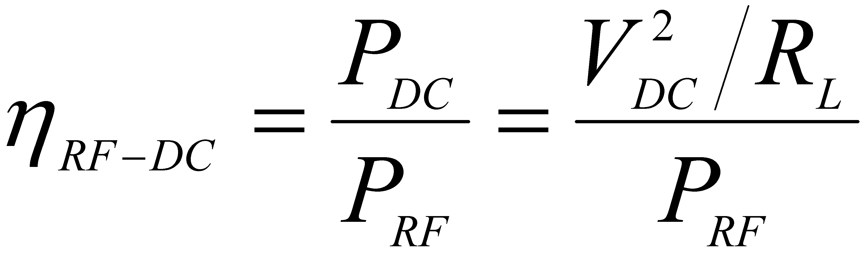
여기서, PDC, PRF, VDC 및 RL 각각은 변환된 DC 파워, 수신 RF 파워, 변환된 DC 전압 및 부하 임피던스를 나타낸다.Here, P DC , P RF , V DC, and R L represent converted DC power, received RF power, converted DC voltage, and load impedance, respectively.
도 4a에 도시한 바와 같은 렉테나의 정류 다이오드(323)는 정류 회로(300)를 설계함에 있어 가장 중요함은 앞서 서술한 바와 같으며, 따라서 본 발명에 따른 렉테나 다이오드는 후술하는 몇 가지 조건에 의해 설정되는 것이 바람직하다. The
본 발명에 따른 다이오드를 위한 조건들은, 높은 입력 파워 효율과 관련한 높은 파괴(breakdown) 전압 Vbr, 작은 신호 검출 능력과 관련한 낮은 포워드 전압 Vf, 정류기의 전반적인 효율과 관련된 낮은 시리즈 저항 Rs, 동작 대역폭과 관련한 낮은 접합 커패시턴스(Junction Capacitance) Cj이다. The conditions for a diode according to the present invention include a high breakdown voltage V br in relation to high input power efficiency, a low forward voltage V f in relation to small signal detection capability, a low series resistance R s associated with the overall efficiency of the rectifier, And a low junction capacitance C j with respect to bandwidth.
본 발명에 따른 다이오드의 바람직한 실시예로는 아바고 테크놀로지사(Avago Technologies)의 패키징된 쇼트기 배리어 다이오드 HSMS-8101를 들 수 있다. 이 다이오드는 10 GHz 내지 14 GHz 주파수 범위에서 최적으로 동작하기 때문에 9.5 GHz에서 사용 가능하다.A preferred embodiment of the diode according to the present invention is the packaged Schottky barrier diode HSMS-8101 from Avago Technologies. These diodes operate at 9.5 GHz because they operate optimally in the 10 GHz to 14 GHz frequency range.
도 4a의 회로에 대한 다이오드 등가 회로인 도 4b를 살펴보면, 시리즈 저항 전압 Rs = 6, 접합 커패시턴스(Junction Capacitance) Cj = 0.17 pF으로 나타나 있으며, 파괴전압 Vbr, 포워드 전압 Vf 은 0.25 ~ 0.35 V, 파괴전압은 Vbr < -4V 이며, 접합 저항 Cj는 동작 조건에 따라 가변적이다. Referring to FIG diode equivalent circuit of Figure 4b for the circuit 4a, a series resistive voltage R s = 6, the junction capacitance (Junction Capacitance) are indicated by C j = 0.17 pF, the breakdown voltage V br, forward voltage V f Is 0.25 to 0.35 V, the breakdown voltage is V br <-4 V, and the junction resistance C j is variable depending on the operating conditions.
이와 같은 조건 하에서 9.5 GHz를 동작 주파수로 하고 10 mW 입력 파워 및 1000 Ω 부하를 가진다고 할 때, 50 Ω 소스 임피던스를 가지는 경우 회로 시뮬레이션을 이용해 다이오드의 입력 임피던스를 계산하면 (22-j20)Ω이 된다. 안테나와 다이오드 간의 임피던스 차이는 파워 전달 및 다이오드 효율의 감소를 가져온다. 따라서, 안테나로부터 다이오드로의 RF 파워 전달을 극대화하기 위해, 임피던스 정합 회로(320)가 도 4a와 같이 설계될 수 있다.Assuming that the operating frequency is 9.5 GHz under these conditions and has a 10 mW input power and a 1000 Ω load, calculating the input impedance of the diode using a circuit simulation with a 50 Ω source impedance is (22-j20) Ω . The impedance difference between the antenna and the diode results in a reduction in power delivery and diode efficiency. Therefore, in order to maximize the transmission of RF power from the antenna to the diode, the
즉, 다이오드의 입력 임피던스는 동작 주파수, RF 입력 파워 및 부하 저항에 따라 변화하기 때문에, 본 발명의 일 실시예에 따른 정합 회로는 도 4a에 도시한 바와 같이 광대역 동작을 위한 두 개의 방사형 스터브(radial stub)를 활용해 구성되는 것이 바람직하다.That is, since the input impedance of the diode changes according to the operating frequency, the RF input power, and the load resistance, the matching circuit according to an embodiment of the present invention includes two radial stubs stub.
이때, 안테나와 다이오드(323) 간의 임피던스 정합을 위한 방사형 스터브는 원주각이 70°인 것이 바람직하다.
At this time, the radial stub for impedance matching between the antenna and the
일반적으로, 다이오드의 비선형 특성은 고차 고조파를 생성하며 이는 RF-DC 변환 효율을 감소시킨다. 그러므로, 고조파 제거 필터(310) 및 DC 패스 필터(330)가 고차 고조파를 억제할 필요가 있다.In general, the nonlinear characteristics of the diodes produce higher order harmonics, which reduces the RF-to-DC conversion efficiency. Therefore, the
도 5a는 입력 고조파 제거 필터의 레이아웃을 나타내며, 도 5b는 입력 고조파 제거 필터의 S21 특성을 나타낸다. FIG. 5A shows the layout of the input harmonic elimination filter, and FIG. 5B shows the S 21 characteristic of the input harmonic elimination filter.
도 5a에 도시한 고조파 제거 필터(310)는 커플드 마이크로스트립 라인들(311) 및 방사형 스터브(312)를 포함할 수 있다.The
고조파 제거 필터(310)는 다이오드(323)로부터 RF 고조파의 재방사를 방지하고 안테나로부터 수신되는 원치 않는 노이즈 신호를 차단한다.The
투과계수 S21은 시뮬레이터(예를 들어, ADS(Advanced Design System) 모멘텀 시뮬레이터)에 의해 분석될 수 있다. 고조파 제거 필터(310)의 커플드 마이크로스트립 밴드-패스 필터(311)는 3 dB에서 9.5 GHz 동작 주파수를 중심으로 하여 7.3 GHz의 대역폭을 갖는다.The transmission coefficient S 21 may be analyzed by a simulator (e.g., ADS (Advanced Design System) momentum simulator). The coupled microstrip band-
정리하면, 밴드-스탑(band-stop) 필터로 동작하는 개방-회로형 방사형 스터브(312) 및 밴드-패스 필터(311)를 포함하는 고조파 제거 필터는 도 5b에 도시된 바와 같이, 19 GHz 근처에서 제1 하모닉 주파수를, 28.5 GHz 근처에서 제2 하모닉 주파수를 감쇠하여, 투과계수 S21을 각각 -26.6 dB, -16.5 dB 감소시킨다. In summary, the harmonic reject filter comprising the open-
이때, RF 신호의 고조파를 제거하기 위한 방사형 스터브(312)는, 도 5a에 도시한 바와 같이, 원주각은 70°인 것이 바람직하다.
At this time, as shown in Fig. 5A, the
도 6a는 DC 패스 필터의 레이아웃을 나타내며, 도 6b는 DC 패스 필터의 S21 특성을 나타낸다. FIG. 6A shows the layout of the DC pass filter, and FIG. 6B shows the S 21 characteristic of the DC pass filter.
본 발명의 일 실시예에 따른 DC 패스 필터(330)는 RF를 감쇠시켜 부하로 DC 파워만을 전달하며, 다이오드(323)의 출력단에 위치할 수 있다. DC 패스 필터(330)는 단일 방사형 스터브(331) 및 대칭으로 배치되는 한 쌍의 방사형 스터브(332)를 포함하며, 기본파, 제2 및 제3 고조파의 투과계수 파라미터인 S21를 15dB보다 더 낮게, 즉, 도 6b에 도시된 바와 같이 -26 dB, -18.8 dB, -25.5 dB 까지 감쇠시킨다. The
이때, DC 파워 전달을 위한 단일 방사형 스터브(331) 또는 RF의 리플 전압을 감소시키기 위한 한 쌍의 방사형 스터브(332)는 도 4a에 도시한 바와 같이, 원주각이 70°인 것이 바람직하다.
At this time, it is preferable that the single
도 7은 다이오드로부터 커패시터까지의 거리에 따른 DC 패스 필터의 변환 효율을 나타낸다.7 shows the conversion efficiency of the DC pass filter according to the distance from the diode to the capacitor.
여기서, 다이오드(323)로부터 커패시터(CL)까지의 거리는 도 4a에 도시한 바와 같이, 도면 부호 d로 나타낼 수 있다.Here, the distance from the
정류 회로(300)에서, 부하와 병렬로 연결되는 커패시터는 리플 전압을 낮추어 부하로 안정적인 DC 파워를 공급한다.In the
도 7을 참조하면, DC 패스 필터(330)는 변화하는 거리에 대해 RF-DC 변환 효율을 거의 상수로 유지시킴을 알 수 있다.Referring to FIG. 7, it can be seen that the
반대로 DC 패스 필터(330)를 사용하지 않는 경우에는, RF-DC 변환 효율이 크게 낮아지고 최대 RF-DC 변환 효율에 대한 최적의 길이가 존재함을 알 수 있다.Conversely, when the
따라서, 본 발명에 따른 DC 패스 필터(330)는 정류 회로(300)의 안정 동작을 위한 주요 요소일 수 있다.
Therefore, the
도 8a는 DC 리턴부의 레이아웃을 나타내며, 도 8b는 DC-리턴부의 S 파라미터를 나타낸다.Fig. 8A shows the layout of the DC return section, and Fig. 8B shows S parameters of the DC-return section.
DC 리턴부(340)는 역전류가 다이오드(323)로 흐를 때 다이오드(323)에 의해 생성된 고조파의 재반사를 방지하는 데 사용된다. DC 리턴부(340)는 접지(도 8a의 포트 3)로부터 정류 회로로의 역전류를 제거하고 안테나로의 RF 재반사를 방지할 수 있다.The
DC 리턴부(340)는 접지(포트 3) 및 포트 1, 2 간의 X-밴드 전달을 막는 밴드-스탑 필터로서 기능할 수 있다.The
반대로, 3.2 ~ 13.5 GHz 주파수(3dB 밴드패스 영역)에서 포트 1로부터 포트 2로의 RF 전달은 접지에 의해 영향을 받지 않는다.Conversely, RF transmission from
이때, 도 8a에 도시한 바와 같이, 접지(포트 3) 및 포트 1, 2 사이에 방사형 스터브를 더 포함할 수 있고, 상기 RF의 리플 전압을 감소시켜 안정적인 DC 파워를 부하로 공급하기 위한 방사형 스터브는 원주각이 70°인 것이 바람직하다.
8A, a radial stub (not shown) may be further included between the ground (port 3) and the
도 9a는 다양한 입력 파워에 대한 본 발명에 따른 정류 회로의 반사계수 S11에 대한 시뮬레이션 결과를, 도 9b는 다양한 입력 파워에 대한 본 발명에 따른 정류 회로의 변환효율에 대한 시뮬레이션 결과를 나타낸다.FIG. 9A shows simulation results for the reflection coefficient S 11 of the rectifying circuit according to the present invention for various input powers, and FIG. 9B shows simulation results for the conversion efficiency of the rectifying circuit according to the present invention for various input powers.
도 9a 및 도 9b는 다양한 동작 조건 하에서 정류 회로 성능의 예측으로서 계산된 S11 및 RF-DC 변환 효율을 보여준다.9A and 9B show S 11 and RF-DC conversion efficiency calculated as a prediction of rectifier circuit performance under various operating conditions.
RF-DC 변환 효율(ηRF - DC)은 50 Ω 내지 1000 Ω의 부하 저항 및 10 dBm, 11 dBm, 12.5 dBm의 입력 파워에 대해, 앞서 설명한 수학식 1에 따라 계산되었다.The RF-to-DC conversion efficiency (η RF - DC ) was calculated according to
다이오드의 입력 임피던스가 동작 조건들에 따라 변화하기 때문에, 도 9a 및 도 9b에 도시한 바와 같이 9.5 GHz에서, 정류 회로가 입력 파워에 따라 부하 저항에 대해 최적화되어 있다. 12.5 dBm의 입력 파워의 경우 400 Ω의 부하 저항일 때, 최대 효율 및 전압이 각각 71 % 및 2.25 V이다.
Since the input impedance of the diode varies with operating conditions, at 9.5 GHz as shown in Figs. 9A and 9B, the rectifier circuit is optimized for the load resistance according to the input power. For a 12.5 dBm input power, the maximum efficiency and voltage are 71% and 2.25 V, respectively, at a load resistance of 400 Ω.
동작 주파수의 변화에 따라 다이오드 및 각 정류 회로 부품들의 임피던스가 변화하기 때문에 광대역 동작을 위한 정류 회로를 설계하는 것은 쉽지 않다. 본 발명에서는 이를 극복하기 위해 앞서 설명한 바와 같이, 광대역 주파수 상에 동작 가능하도록 방사형 스터브를 이용해 정류회로 부품들을 설계하였다.
It is not easy to design a rectifier circuit for wideband operation because the impedance of the diode and each rectifier circuit component changes with the change of the operating frequency. In order to overcome this problem, in the present invention, as described above, rectifier circuit components are designed using a radial stub so as to be operable on a wide frequency band.
도 10a 및 도 10b는 다양한 입력 파워에 대해 주파수 대비 S11 및 RF-DC 변환 효율에 대한 시뮬레이션 값을 나타낸 그래프이다. 10A and 10B are graphs showing simulation values for S 11 and RF-DC conversion efficiency versus frequency for various input powers.
도 10a에 나타나 시뮬레이션 결과를 살펴보면 8.8 내지 9.9 GHz 주파수 범위에서 10dB보다 낮은 반사계수 S11을 나타내고 있음을 알 수 있다. 또한, 도 10b에서 12.5 dBm의 입력 파워에 대해 9.1 내지 10.2 GHz 주파수 범위에서 RF-DC 변환 효율(ηRF-DC)이 50% 이상임을 확인할 수 있다.
10A, the simulation result shows that the reflection coefficient S 11 is lower than 10 dB in the frequency range of 8.8 to 9.9 GHz. 10B, it can be confirmed that the RF-DC conversion efficiency (? RF-DC ) is 50% or more in the frequency range of 9.1 to 10.2 GHz for an input power of 12.5 dBm.
도 11a 및 도 11b는 다양한 부하에 대해 실제 측정한 입력파워 대비 RF-DC 변환 효율 및 변환 전압을 나타낸 그래프이다.FIGS. 11A and 11B are graphs showing RF-DC conversion efficiency and converted voltage versus actual measured input power for various loads. FIG.
도 11a에 도시된 입력파워 대비 측정된 RF-DC 변환 효율의 전체적인 경향은 시뮬레이션 결과와 유사함을 알 수 있다. 하지만, 최대 RF-DC 변환 효율에 대한 최적 조건은 조금 다른 양상이다. 400 Ω의 부하에서 12.5 dBm에 대한 RF-DC 변환 효율의 시뮬레이션 값은 71%이지만, 측정치의 경우에는 300 Ω의 부하일 때 17 dBm에 대해 71.9%의 효율이 나타났다. 측정 결과로부터, 본 발명에 따른 다이오드 및 정류 회로가 시뮬레이션 값보다 더 높은 입력 파워에서 사용될 수 있음이 드러났다. The overall tendency of the measured RF-DC conversion efficiency versus the input power shown in FIG. 11A is similar to the simulation result. However, the optimum conditions for maximum RF-to-DC conversion efficiency are slightly different. The simulation value of RF-DC conversion efficiency to 12.5 dBm at a load of 400 Ω is 71%, but the measured value shows 71.9% efficiency for 17 dBm at a load of 300 Ω. From the measurement results it has been found that the diode and rectifier circuit according to the invention can be used at higher input power than the simulation value.
도 11b를 살펴보면, 입력 파워가 증가할수록 변환된 DC 전압 또한 증가하며, 최대 효율에서의 DC 전압은 3.2 V 임을 알 수 있다. Referring to FIG. 11B, it can be seen that as the input power increases, the converted DC voltage also increases, and the DC voltage at the maximum efficiency is 3.2V.
8.51 GHz에서 63.2 %, 혹은 9.3 GHz에서 21 %의 효율을 보였던 기존의 변환 회로와 비교하면, 본 발명에 따른 RF-DC 변환 회로는 X-밴드에서 이러한 기존의 회로들보다 높은 효율을 보여주고 있음을 확인할 수 있다.
The RF-DC conversion circuit according to the present invention shows higher efficiency than the conventional circuits in the X-band in comparison with the conventional conversion circuit which showed efficiency of 63.2% at 8.51 GHz or 21% at 9.3 GHz can confirm.
도 12a 및 도 12b는 본 발명의 일 실시예에 따라 측정된 변환 효율 및 변환 전압을 나타낸 그래프이다. 12A and 12B are graphs showing conversion efficiency and conversion voltage measured according to an embodiment of the present invention.
도 12a를 살펴보면, 본 발명에 따른 정류 회로가 71.9 %의 최대 효율을 가지며 1 GHz 이상의 주파수 대역폭에서 50 % 이상의 효율을 유지함을 알 수 있다.12A, it can be seen that the rectifying circuit according to the present invention has a maximum efficiency of 71.9% and maintains an efficiency of 50% or more in a frequency bandwidth of 1 GHz or more.
본 발명에 따른 정류 회로는 9.5 GHz에서 동작하는 35 mm×21 mm 사이즈로 콤팩트하게 최적화되어 대형 렉테나 어레이 시스템에 적용할 수 있다.
The rectifier circuit according to the present invention can be compactly optimized to a size of 35 mm x 21 mm which operates at 9.5 GHz and can be applied to a large rectenna array system.
이상 실시예를 참조하여 설명하였지만, 해당 기술 분야의 숙련된 당업자는 하기의 특허 청구의 범위에 기재된 본 발명의 사상 및 영역으로부터 벗어나지 않는 범위 내에서 본 발명을 다양하게 수정 및 변경시킬 수 있음을 이해할 수 있을 것이다.
It will be understood by those skilled in the art that various changes in form and details may be made therein without departing from the spirit and scope of the invention as defined in the appended claims. It will be possible.
210, 230: 제1 패치, 제2 패치 기판
220: 폼 기판
240: 수평/수직 슬롯 기판
250: 피드라인 기판
260: 피드 라인
300: 정류 회로
310: 고조파 제거 필터
320: 정합부
323: 정류 다이오드
330: DC 패스 필터
340: DC 리턴부210, 230: first patch, second patch substrate 220: foam substrate
240: Horizontal / Vertical Slot Substrate 250: Feed Line Substrate
260: feed line 300: rectifying circuit
310: Harmonic elimination filter 320:
323: rectifier diode 330: DC pass filter
340: DC return portion
Claims (20)
상기 원형 편파 패치 안테나가 수신한 RF 신호를 DC(Direct Current) 신호로 변환하여 출력함으로써 상기 안테나로부터 부하로 DC 파워를 전달하는 정류 회로;를 포함하되,
상기 정류 회로는, 적어도 하나의 방사형(radial) 스터브를 포함하는 것을 특징으로 하는 렉테나.A circularly polarized patch antenna for receiving an RF (Radio Frequency) signal; And
And a rectifying circuit for converting the RF signal received by the circularly polarized patch antenna into a DC (direct current) signal and transmitting the DC signal to the load from the antenna,
Characterized in that the rectifying circuit comprises at least one radial stub.
상기 방사형 스터브는,
RF 신호의 고조파 제거에 이용되는 제1 방사형 스터브, 상기 안테나와 정류 다이오드 간의 임피던스 정합에 이용되는 제2 방사형 스터브, DC 파워 전달에 사용되는 제3 방사형 스터브 및 RF의 리플 전압을 감소시켜 안정적인 DC 파워를 부하로 공급하는 데 사용되는 제4 방사형 스터브 중 적어도 하나를 포함하는 것을 특징으로 하는 렉테나.The method according to claim 1,
The radial stub includes:
A first radial stub used for harmonic rejection of the RF signal, a second radial stub used for impedance matching between the antenna and the rectifying diode, a third radial stub used for DC power delivery, And a fourth radial stub that is used to feed the load to the load.
상기 제1 방사형 스터브는 밴드-스탑 필터로서 동작하는 것을 특징으로 하는 렉테나.3. The method of claim 2,
Wherein the first radial stub operates as a band-stop filter.
상기 원형 편파 패치 안테나는,
제1 패치가 배치된 제1 패치 기판;
제2 패치가 배치된 제2 패치 기판;
상기 제1 패치 기판 및 제2 패치 기판 사이에 배치되는 폼 기판; 및
상기 제2 패치 하부에 부착되는 피드 라인 기판을 포함하는 것을 특징으로 하는 렉테나. The method according to claim 1,
The circularly polarized patch antenna includes:
A first patch substrate on which a first patch is disposed;
A second patch substrate on which a second patch is disposed;
A foam substrate disposed between the first patch substrate and the second patch substrate; And
And a feed line substrate attached to a lower portion of the second patch.
상기 피드 라인 기판은,
H-형상의 듀얼 슬롯;
상기 H-형상의 듀얼 슬롯을 피드하는 T-형상의 피드 라인; 및
상기 피드 라인에 전력을 분배 공급하는 전력 분배기를 포함하는 것을 특징으로 하는 렉테나.5. The method of claim 4,
Wherein the feed line substrate comprises:
H-shaped dual slot;
A T-shaped feed line feeding the H-shaped dual slot; And
And a power divider for distributing power to the feed line.
상기 정류 회로는,
커플드 마이크로스트립 라인 및 제1 방사형 스터브를 포함하고, RF 고조파의 재방사를 방지하는 고조파 제거부;
상기 고조파 제거부의 출력단에 위치하며, 제2 방사형 스터브를 포함하여 안테나와 정류 다이오드 간의 임피던스 정합을 수행하는 정합부;
상기 정합부의 출력단에 위치하는 정류 다이오드;
제3 방사형 스터브를 포함하여 상기 정류 다이오드가 출력하는 RF를 감쇠시켜 DC 파워를 전달하는 DC 패스 필터; 및
제4 방사형 스터브를 포함하여 상기 DC 패스 필터가 출력하는 신호에서 리플 전압을 감소시켜 안정적인 DC 파워를 부하로 공급하는 DC 리턴부를 포함하는 것을 특징으로 하는 렉테나.The method according to claim 1,
The rectifying circuit includes:
A harmonic eliminator comprising a coupled microstrip line and a first radial stub, the harmonic eliminator preventing re-emission of RF harmonics;
A matching unit located at an output terminal of the harmonic removing unit and including a second radial stub to perform impedance matching between the antenna and the rectifying diode;
A rectifying diode located at an output terminal of the matching unit;
A DC pass filter including a third radial stub to attenuate RF output from the rectifying diode to deliver DC power; And
And a DC returning part including a fourth radial stub for reducing a ripple voltage in a signal output from the DC pass filter to supply stable DC power to the load.
상기 고조파 제거부는 안테나로부터 유입되는 노이즈 신호를 차단하는 것을 특징으로 하는 렉테나.The method according to claim 6,
And the harmonic elimination unit blocks the noise signal flowing from the antenna.
상기 커플드 마이크로스트립 라인은 밴드패스 필터로 동작하는 것을 특징으로 하는 렉테나.The method according to claim 6,
Wherein the coupled microstrip line operates as a band-pass filter.
상기 방사형 스터브는 원주각이 70 °인 것을 특징으로 하는 렉테나.The method according to claim 1,
Wherein the radial stub has a circumferential angle of 70 [deg.].
상기 정류 회로는, 동작 주파수가 9.5 GHz 부근인 것을 특징으로 하는 렉테나.The method according to claim 1,
Wherein the rectifying circuit has an operating frequency of about 9.5 GHz.
상기 고조파 제거부의 출력단에 위치하며, 제2 방사형 스터브를 포함하여 안테나와 정류 다이오드 간의 임피던스 정합을 수행하는 정합부;
상기 정합부의 출력단에 위치하는 정류 다이오드;
제3 방사형 스터브를 포함하여 상기 정류 다이오드가 출력하는 RF를 감쇠시켜 DC 파워를 전달하는 DC 패스 필터; 및
제4 방사형 스터브를 포함하여 상기 DC 패스부가 출력하는 신호에서 리플 전압을 감소시켜 안정적인 DC 파워를 부하로 공급하는 DC 리턴부를 포함하는 것을 특징으로 하는 정류 장치.A harmonic eliminator comprising a coupled microstrip line and a first radial stub, the harmonic eliminator preventing re-emission of RF harmonics;
A matching unit located at an output terminal of the harmonic removing unit and including a second radial stub to perform impedance matching between the antenna and the rectifying diode;
A rectifying diode located at an output terminal of the matching unit;
A DC pass filter including a third radial stub to attenuate RF output from the rectifying diode to deliver DC power; And
And a DC returning unit including a fourth radial stub for reducing a ripple voltage in a signal output from the DC path unit and supplying stable DC power to the load.
상기 커플드 마이크로스트립 라인은 밴드패스 필터로 동작하는 것을 특징으로 하는 정류 장치.12. The method of claim 11,
Wherein the coupled microstrip line operates as a band-pass filter.
상기 제1 방사형 스터브는 개방 회로형 방사형 스터브이고, 밴드-스탑 필터로 동작하는 것을 특징으로 하는 정류 장치. 12. The method of claim 11,
Wherein the first radial stub is an open circuit radial stub and operates as a band-stop filter.
상기 제2 방사형 스터브는 대칭으로 배치된 두 개의 방사형 스터브를 포함하는 것을 특징으로 하는 정류 장치.12. The method of claim 11,
Wherein the second radial stub comprises two radial stubs arranged symmetrically.
상기 제3 방사형 스터브는 단일 방사형 스터브 및 한 쌍의 대칭 방사형 스터브를 포함하는 것을 특징으로 하는 정류 장치.12. The method of claim 11,
Wherein the third radial stub comprises a single radial stub and a pair of symmetrical radial stubs.
상기 제4 방사형 스터브는 단일 방사형 스터브를 포함하는 것을 특징으로 하는 정류 장치.12. The method of claim 11,
And said fourth radial stub comprises a single radial stub.
상기 고조파 제거부는 안테나로부터 유입되는 노이즈 신호를 차단하는 것을 특징으로 하는 정류 장치.12. The method of claim 11,
And the harmonic elimination unit blocks the noise signal flowing from the antenna.
상기 제1 방사형 스터브는 밴드-스탑 필터로 동작하는 것을 특징으로 하는 정류 장치.12. The method of claim 11,
Wherein the first radial stub operates as a band-stop filter.
상기 제1 내지 제4 방사형 스터브는 원주각이 70°인 것을 특징으로 하는 정류 장치.12. The method of claim 11,
Wherein the first to fourth radial stubs have a circumferential angle of 70 °.
상기 정류 장치는, 동작 주파수가 9.5 GHz 부근인 것을 특징으로 하는 정류 장치.12. The method of claim 11,
Wherein the rectifying device has an operating frequency in the vicinity of 9.5 GHz.
Priority Applications (2)
| Application Number | Priority Date | Filing Date | Title |
|---|---|---|---|
| KR1020140128530A KR101640785B1 (en) | 2014-09-25 | 2014-09-25 | Wideband rectenna and rectifying apparatus for rectenna |
| US14/645,479 US9472849B2 (en) | 2014-09-25 | 2015-03-12 | Wideband rectenna and rectifying apparatus for rectenna |
Applications Claiming Priority (1)
| Application Number | Priority Date | Filing Date | Title |
|---|---|---|---|
| KR1020140128530A KR101640785B1 (en) | 2014-09-25 | 2014-09-25 | Wideband rectenna and rectifying apparatus for rectenna |
Publications (2)
| Publication Number | Publication Date |
|---|---|
| KR20160036372A true KR20160036372A (en) | 2016-04-04 |
| KR101640785B1 KR101640785B1 (en) | 2016-07-19 |
Family
ID=55585505
Family Applications (1)
| Application Number | Title | Priority Date | Filing Date |
|---|---|---|---|
| KR1020140128530A KR101640785B1 (en) | 2014-09-25 | 2014-09-25 | Wideband rectenna and rectifying apparatus for rectenna |
Country Status (2)
| Country | Link |
|---|---|
| US (1) | US9472849B2 (en) |
| KR (1) | KR101640785B1 (en) |
Cited By (2)
| Publication number | Priority date | Publication date | Assignee | Title |
|---|---|---|---|---|
| CN109193143A (en) * | 2018-09-06 | 2019-01-11 | 清华四川能源互联网研究院 | A kind of low power microwave receiving rectification antenna |
| KR20220159708A (en) * | 2021-05-26 | 2022-12-05 | 인천대학교 산학협력단 | Dual band multi-beam antenna apparauts with frequency divider/combiner and multi-beam antenna for 5g mobile communication |
Families Citing this family (152)
| Publication number | Priority date | Publication date | Assignee | Title |
|---|---|---|---|---|
| US10965164B2 (en) | 2012-07-06 | 2021-03-30 | Energous Corporation | Systems and methods of wirelessly delivering power to a receiver device |
| US10008889B2 (en) | 2014-08-21 | 2018-06-26 | Energous Corporation | Method for automatically testing the operational status of a wireless power receiver in a wireless power transmission system |
| US10381880B2 (en) | 2014-07-21 | 2019-08-13 | Energous Corporation | Integrated antenna structure arrays for wireless power transmission |
| US10199849B1 (en) | 2014-08-21 | 2019-02-05 | Energous Corporation | Method for automatically testing the operational status of a wireless power receiver in a wireless power transmission system |
| US10211680B2 (en) | 2013-07-19 | 2019-02-19 | Energous Corporation | Method for 3 dimensional pocket-forming |
| US9812890B1 (en) | 2013-07-11 | 2017-11-07 | Energous Corporation | Portable wireless charging pad |
| US10128699B2 (en) | 2014-07-14 | 2018-11-13 | Energous Corporation | Systems and methods of providing wireless power using receiver device sensor inputs |
| US10124754B1 (en) | 2013-07-19 | 2018-11-13 | Energous Corporation | Wireless charging and powering of electronic sensors in a vehicle |
| US10063106B2 (en) | 2014-05-23 | 2018-08-28 | Energous Corporation | System and method for a self-system analysis in a wireless power transmission network |
| US10218227B2 (en) | 2014-05-07 | 2019-02-26 | Energous Corporation | Compact PIFA antenna |
| US10291055B1 (en) | 2014-12-29 | 2019-05-14 | Energous Corporation | Systems and methods for controlling far-field wireless power transmission based on battery power levels of a receiving device |
| US10992185B2 (en) | 2012-07-06 | 2021-04-27 | Energous Corporation | Systems and methods of using electromagnetic waves to wirelessly deliver power to game controllers |
| US9438045B1 (en) | 2013-05-10 | 2016-09-06 | Energous Corporation | Methods and systems for maximum power point transfer in receivers |
| US10439448B2 (en) | 2014-08-21 | 2019-10-08 | Energous Corporation | Systems and methods for automatically testing the communication between wireless power transmitter and wireless power receiver |
| US10206185B2 (en) | 2013-05-10 | 2019-02-12 | Energous Corporation | System and methods for wireless power transmission to an electronic device in accordance with user-defined restrictions |
| US10270261B2 (en) | 2015-09-16 | 2019-04-23 | Energous Corporation | Systems and methods of object detection in wireless power charging systems |
| US9843201B1 (en) | 2012-07-06 | 2017-12-12 | Energous Corporation | Wireless power transmitter that selects antenna sets for transmitting wireless power to a receiver based on location of the receiver, and methods of use thereof |
| US10063064B1 (en) | 2014-05-23 | 2018-08-28 | Energous Corporation | System and method for generating a power receiver identifier in a wireless power network |
| US10199835B2 (en) | 2015-12-29 | 2019-02-05 | Energous Corporation | Radar motion detection using stepped frequency in wireless power transmission system |
| US10223717B1 (en) | 2014-05-23 | 2019-03-05 | Energous Corporation | Systems and methods for payment-based authorization of wireless power transmission service |
| US10211682B2 (en) | 2014-05-07 | 2019-02-19 | Energous Corporation | Systems and methods for controlling operation of a transmitter of a wireless power network based on user instructions received from an authenticated computing device powered or charged by a receiver of the wireless power network |
| US9887584B1 (en) | 2014-08-21 | 2018-02-06 | Energous Corporation | Systems and methods for a configuration web service to provide configuration of a wireless power transmitter within a wireless power transmission system |
| US10312715B2 (en) | 2015-09-16 | 2019-06-04 | Energous Corporation | Systems and methods for wireless power charging |
| US10205239B1 (en) | 2014-05-07 | 2019-02-12 | Energous Corporation | Compact PIFA antenna |
| US10263432B1 (en) | 2013-06-25 | 2019-04-16 | Energous Corporation | Multi-mode transmitter with an antenna array for delivering wireless power and providing Wi-Fi access |
| US9871398B1 (en) | 2013-07-01 | 2018-01-16 | Energous Corporation | Hybrid charging method for wireless power transmission based on pocket-forming |
| US10141791B2 (en) | 2014-05-07 | 2018-11-27 | Energous Corporation | Systems and methods for controlling communications during wireless transmission of power using application programming interfaces |
| US9867062B1 (en) | 2014-07-21 | 2018-01-09 | Energous Corporation | System and methods for using a remote server to authorize a receiving device that has requested wireless power and to determine whether another receiving device should request wireless power in a wireless power transmission system |
| US9825674B1 (en) | 2014-05-23 | 2017-11-21 | Energous Corporation | Enhanced transmitter that selects configurations of antenna elements for performing wireless power transmission and receiving functions |
| US10243414B1 (en) | 2014-05-07 | 2019-03-26 | Energous Corporation | Wearable device with wireless power and payload receiver |
| US20150326070A1 (en) | 2014-05-07 | 2015-11-12 | Energous Corporation | Methods and Systems for Maximum Power Point Transfer in Receivers |
| US9787103B1 (en) | 2013-08-06 | 2017-10-10 | Energous Corporation | Systems and methods for wirelessly delivering power to electronic devices that are unable to communicate with a transmitter |
| US9876394B1 (en) | 2014-05-07 | 2018-01-23 | Energous Corporation | Boost-charger-boost system for enhanced power delivery |
| US10230266B1 (en) | 2014-02-06 | 2019-03-12 | Energous Corporation | Wireless power receivers that communicate status data indicating wireless power transmission effectiveness with a transmitter using a built-in communications component of a mobile device, and methods of use thereof |
| US10256657B2 (en) | 2015-12-24 | 2019-04-09 | Energous Corporation | Antenna having coaxial structure for near field wireless power charging |
| US10193396B1 (en) | 2014-05-07 | 2019-01-29 | Energous Corporation | Cluster management of transmitters in a wireless power transmission system |
| US10148097B1 (en) | 2013-11-08 | 2018-12-04 | Energous Corporation | Systems and methods for using a predetermined number of communication channels of a wireless power transmitter to communicate with different wireless power receivers |
| US11502551B2 (en) | 2012-07-06 | 2022-11-15 | Energous Corporation | Wirelessly charging multiple wireless-power receivers using different subsets of an antenna array to focus energy at different locations |
| US10063105B2 (en) | 2013-07-11 | 2018-08-28 | Energous Corporation | Proximity transmitters for wireless power charging systems |
| US10211674B1 (en) | 2013-06-12 | 2019-02-19 | Energous Corporation | Wireless charging using selected reflectors |
| US9124125B2 (en) | 2013-05-10 | 2015-09-01 | Energous Corporation | Wireless power transmission with selective range |
| US10992187B2 (en) | 2012-07-06 | 2021-04-27 | Energous Corporation | System and methods of using electromagnetic waves to wirelessly deliver power to electronic devices |
| US9853458B1 (en) | 2014-05-07 | 2017-12-26 | Energous Corporation | Systems and methods for device and power receiver pairing |
| US10291066B1 (en) | 2014-05-07 | 2019-05-14 | Energous Corporation | Power transmission control systems and methods |
| US9859797B1 (en) | 2014-05-07 | 2018-01-02 | Energous Corporation | Synchronous rectifier design for wireless power receiver |
| US10128693B2 (en) | 2014-07-14 | 2018-11-13 | Energous Corporation | System and method for providing health safety in a wireless power transmission system |
| US10090886B1 (en) | 2014-07-14 | 2018-10-02 | Energous Corporation | System and method for enabling automatic charging schedules in a wireless power network to one or more devices |
| US10186913B2 (en) | 2012-07-06 | 2019-01-22 | Energous Corporation | System and methods for pocket-forming based on constructive and destructive interferences to power one or more wireless power receivers using a wireless power transmitter including a plurality of antennas |
| US10224758B2 (en) | 2013-05-10 | 2019-03-05 | Energous Corporation | Wireless powering of electronic devices with selective delivery range |
| US10141768B2 (en) | 2013-06-03 | 2018-11-27 | Energous Corporation | Systems and methods for maximizing wireless power transfer efficiency by instructing a user to change a receiver device's position |
| US10038337B1 (en) | 2013-09-16 | 2018-07-31 | Energous Corporation | Wireless power supply for rescue devices |
| US10090699B1 (en) | 2013-11-01 | 2018-10-02 | Energous Corporation | Wireless powered house |
| US10103582B2 (en) | 2012-07-06 | 2018-10-16 | Energous Corporation | Transmitters for wireless power transmission |
| US11843260B2 (en) | 2012-11-09 | 2023-12-12 | California Institute Of Technology | Generator unit for wireless power transfer |
| US10367380B2 (en) | 2012-11-09 | 2019-07-30 | California Institute Of Technology | Smart RF lensing: efficient, dynamic and mobile wireless power transfer |
| US11616520B2 (en) | 2012-11-09 | 2023-03-28 | California Institute Of Technology | RF receiver |
| US10103552B1 (en) | 2013-06-03 | 2018-10-16 | Energous Corporation | Protocols for authenticated wireless power transmission |
| US10021523B2 (en) | 2013-07-11 | 2018-07-10 | Energous Corporation | Proximity transmitters for wireless power charging systems |
| EP3072214B1 (en) | 2013-11-22 | 2018-10-10 | California Institute of Technology | Generator unit for wireless power transfer |
| EP3072213B1 (en) | 2013-11-22 | 2020-01-22 | California Institute Of Technology | Active cmos recovery units for wireless power transmission |
| US10075017B2 (en) | 2014-02-06 | 2018-09-11 | Energous Corporation | External or internal wireless power receiver with spaced-apart antenna elements for charging or powering mobile devices using wirelessly delivered power |
| US10158257B2 (en) | 2014-05-01 | 2018-12-18 | Energous Corporation | System and methods for using sound waves to wirelessly deliver power to electronic devices |
| US10153653B1 (en) | 2014-05-07 | 2018-12-11 | Energous Corporation | Systems and methods for using application programming interfaces to control communications between a transmitter and a receiver |
| US10170917B1 (en) | 2014-05-07 | 2019-01-01 | Energous Corporation | Systems and methods for managing and controlling a wireless power network by establishing time intervals during which receivers communicate with a transmitter |
| US10153645B1 (en) | 2014-05-07 | 2018-12-11 | Energous Corporation | Systems and methods for designating a master power transmitter in a cluster of wireless power transmitters |
| US10116143B1 (en) | 2014-07-21 | 2018-10-30 | Energous Corporation | Integrated antenna arrays for wireless power transmission |
| US10068703B1 (en) | 2014-07-21 | 2018-09-04 | Energous Corporation | Integrated miniature PIFA with artificial magnetic conductor metamaterials |
| KR102288706B1 (en) | 2014-08-19 | 2021-08-10 | 캘리포니아 인스티튜트 오브 테크놀로지 | Wirelss power transfer |
| US10122415B2 (en) | 2014-12-27 | 2018-11-06 | Energous Corporation | Systems and methods for assigning a set of antennas of a wireless power transmitter to a wireless power receiver based on a location of the wireless power receiver |
| GB2538576B (en) * | 2015-09-14 | 2017-06-14 | Drayson Tech (Europe) Ltd | RF-to-DC Converter |
| GB2538575B (en) * | 2015-09-14 | 2017-06-14 | Drayson Tech (Europe) Ltd | RF-to-DC Converter |
| US10523033B2 (en) | 2015-09-15 | 2019-12-31 | Energous Corporation | Receiver devices configured to determine location within a transmission field |
| US11710321B2 (en) | 2015-09-16 | 2023-07-25 | Energous Corporation | Systems and methods of object detection in wireless power charging systems |
| US10211685B2 (en) | 2015-09-16 | 2019-02-19 | Energous Corporation | Systems and methods for real or near real time wireless communications between a wireless power transmitter and a wireless power receiver |
| US10199850B2 (en) | 2015-09-16 | 2019-02-05 | Energous Corporation | Systems and methods for wirelessly transmitting power from a transmitter to a receiver by determining refined locations of the receiver in a segmented transmission field associated with the transmitter |
| US10158259B1 (en) | 2015-09-16 | 2018-12-18 | Energous Corporation | Systems and methods for identifying receivers in a transmission field by transmitting exploratory power waves towards different segments of a transmission field |
| US10186893B2 (en) | 2015-09-16 | 2019-01-22 | Energous Corporation | Systems and methods for real time or near real time wireless communications between a wireless power transmitter and a wireless power receiver |
| US9871387B1 (en) | 2015-09-16 | 2018-01-16 | Energous Corporation | Systems and methods of object detection using one or more video cameras in wireless power charging systems |
| US10008875B1 (en) | 2015-09-16 | 2018-06-26 | Energous Corporation | Wireless power transmitter configured to transmit power waves to a predicted location of a moving wireless power receiver |
| US10778041B2 (en) | 2015-09-16 | 2020-09-15 | Energous Corporation | Systems and methods for generating power waves in a wireless power transmission system |
| US10027168B2 (en) | 2015-09-22 | 2018-07-17 | Energous Corporation | Systems and methods for generating and transmitting wireless power transmission waves using antennas having a spacing that is selected by the transmitter |
| US10033222B1 (en) | 2015-09-22 | 2018-07-24 | Energous Corporation | Systems and methods for determining and generating a waveform for wireless power transmission waves |
| US10050470B1 (en) | 2015-09-22 | 2018-08-14 | Energous Corporation | Wireless power transmission device having antennas oriented in three dimensions |
| US10020678B1 (en) | 2015-09-22 | 2018-07-10 | Energous Corporation | Systems and methods for selecting antennas to generate and transmit power transmission waves |
| US10153660B1 (en) | 2015-09-22 | 2018-12-11 | Energous Corporation | Systems and methods for preconfiguring sensor data for wireless charging systems |
| US10135295B2 (en) | 2015-09-22 | 2018-11-20 | Energous Corporation | Systems and methods for nullifying energy levels for wireless power transmission waves |
| US10128686B1 (en) | 2015-09-22 | 2018-11-13 | Energous Corporation | Systems and methods for identifying receiver locations using sensor technologies |
| US10135294B1 (en) | 2015-09-22 | 2018-11-20 | Energous Corporation | Systems and methods for preconfiguring transmission devices for power wave transmissions based on location data of one or more receivers |
| US10333332B1 (en) | 2015-10-13 | 2019-06-25 | Energous Corporation | Cross-polarized dipole antenna |
| US10734717B2 (en) | 2015-10-13 | 2020-08-04 | Energous Corporation | 3D ceramic mold antenna |
| GB201518859D0 (en) * | 2015-10-23 | 2015-12-09 | Airbus Defence & Space Ltd | High-efficiency amplifier |
| US9853485B2 (en) | 2015-10-28 | 2017-12-26 | Energous Corporation | Antenna for wireless charging systems |
| US10027180B1 (en) * | 2015-11-02 | 2018-07-17 | Energous Corporation | 3D triple linear antenna that acts as heat sink |
| US10135112B1 (en) | 2015-11-02 | 2018-11-20 | Energous Corporation | 3D antenna mount |
| US10063108B1 (en) | 2015-11-02 | 2018-08-28 | Energous Corporation | Stamped three-dimensional antenna |
| US10038332B1 (en) | 2015-12-24 | 2018-07-31 | Energous Corporation | Systems and methods of wireless power charging through multiple receiving devices |
| US10079515B2 (en) | 2016-12-12 | 2018-09-18 | Energous Corporation | Near-field RF charging pad with multi-band antenna element with adaptive loading to efficiently charge an electronic device at any position on the pad |
| US10256677B2 (en) | 2016-12-12 | 2019-04-09 | Energous Corporation | Near-field RF charging pad with adaptive loading to efficiently charge an electronic device at any position on the pad |
| US10027159B2 (en) | 2015-12-24 | 2018-07-17 | Energous Corporation | Antenna for transmitting wireless power signals |
| US10277054B2 (en) | 2015-12-24 | 2019-04-30 | Energous Corporation | Near-field charging pad for wireless power charging of a receiver device that is temporarily unable to communicate |
| US11863001B2 (en) | 2015-12-24 | 2024-01-02 | Energous Corporation | Near-field antenna for wireless power transmission with antenna elements that follow meandering patterns |
| US10320446B2 (en) | 2015-12-24 | 2019-06-11 | Energous Corporation | Miniaturized highly-efficient designs for near-field power transfer system |
| US10008886B2 (en) | 2015-12-29 | 2018-06-26 | Energous Corporation | Modular antennas with heat sinks in wireless power transmission systems |
| FR3057401B1 (en) * | 2016-10-06 | 2019-08-09 | Universite Paris Est Marne La Vallee | RADIO RECEIVER RECLAIMING DEVICE OF RECENT TYPE |
| US10923954B2 (en) | 2016-11-03 | 2021-02-16 | Energous Corporation | Wireless power receiver with a synchronous rectifier |
| US9966656B1 (en) | 2016-11-08 | 2018-05-08 | Aeternum LLC | Broadband rectenna |
| KR102485241B1 (en) * | 2016-11-14 | 2023-01-06 | 삼성전자주식회사 | Hybrid antenna |
| KR102226403B1 (en) | 2016-12-12 | 2021-03-12 | 에너저스 코포레이션 | Methods of selectively activating antenna zones of a near-field charging pad to maximize wireless power delivered |
| US10389161B2 (en) | 2017-03-15 | 2019-08-20 | Energous Corporation | Surface mount dielectric antennas for wireless power transmitters |
| US10680319B2 (en) | 2017-01-06 | 2020-06-09 | Energous Corporation | Devices and methods for reducing mutual coupling effects in wireless power transmission systems |
| US10439442B2 (en) | 2017-01-24 | 2019-10-08 | Energous Corporation | Microstrip antennas for wireless power transmitters |
| CN106899093B (en) * | 2017-03-15 | 2023-04-21 | 华南理工大学 | Wide power range rectifying circuit adopting reflected power recovery network |
| WO2018183892A1 (en) | 2017-03-30 | 2018-10-04 | Energous Corporation | Flat antennas having two or more resonant frequencies for use in wireless power transmission systems |
| US10854960B2 (en) * | 2017-05-02 | 2020-12-01 | Richard A. Bean | Electromagnetic energy harvesting devices and methods |
| US10511097B2 (en) | 2017-05-12 | 2019-12-17 | Energous Corporation | Near-field antennas for accumulating energy at a near-field distance with minimal far-field gain |
| US11462949B2 (en) | 2017-05-16 | 2022-10-04 | Wireless electrical Grid LAN, WiGL Inc | Wireless charging method and system |
| CN108964292A (en) * | 2017-05-17 | 2018-12-07 | 富泰华工业(深圳)有限公司 | Electronic device |
| WO2018218252A1 (en) | 2017-05-26 | 2018-11-29 | California Institute Of Technology | Method and apparatus for dynamic rf lens focusing and tracking of wireless power recovery unit |
| US10848853B2 (en) | 2017-06-23 | 2020-11-24 | Energous Corporation | Systems, methods, and devices for utilizing a wire of a sound-producing device as an antenna for receipt of wirelessly delivered power |
| US11133576B2 (en) | 2017-08-28 | 2021-09-28 | Aeternum, LLC | Rectenna |
| RU2652168C1 (en) | 2017-09-07 | 2018-04-25 | Самсунг Электроникс Ко., Лтд. | Device for conversion of electromagnetic radiation into direct current |
| US10122219B1 (en) | 2017-10-10 | 2018-11-06 | Energous Corporation | Systems, methods, and devices for using a battery as a antenna for receiving wirelessly delivered power from radio frequency power waves |
| US11342798B2 (en) | 2017-10-30 | 2022-05-24 | Energous Corporation | Systems and methods for managing coexistence of wireless-power signals and data signals operating in a same frequency band |
| CN107947389B (en) * | 2017-11-06 | 2021-09-14 | 电子科技大学 | 2.45GHz microwave power transmission system based on phase control |
| US10615647B2 (en) | 2018-02-02 | 2020-04-07 | Energous Corporation | Systems and methods for detecting wireless power receivers and other objects at a near-field charging pad |
| CN108417978B (en) * | 2018-02-14 | 2023-08-11 | 深圳市道通智能航空技术股份有限公司 | Unmanned aerial vehicle built-in dual-frenquency antenna and unmanned aerial vehicle |
| US11159057B2 (en) | 2018-03-14 | 2021-10-26 | Energous Corporation | Loop antennas with selectively-activated feeds to control propagation patterns of wireless power signals |
| US11515732B2 (en) | 2018-06-25 | 2022-11-29 | Energous Corporation | Power wave transmission techniques to focus wirelessly delivered power at a receiving device |
| GB201811909D0 (en) | 2018-07-20 | 2018-09-05 | Buchanan Nigel Alexander | Screwdriver |
| US11437735B2 (en) | 2018-11-14 | 2022-09-06 | Energous Corporation | Systems for receiving electromagnetic energy using antennas that are minimally affected by the presence of the human body |
| JP2022523022A (en) | 2019-01-28 | 2022-04-21 | エナージャス コーポレイション | Systems and methods for small antennas for wireless power transfer |
| KR20210123329A (en) | 2019-02-06 | 2021-10-13 | 에너저스 코포레이션 | System and method for estimating optimal phase for use with individual antennas in an antenna array |
| WO2020184205A1 (en) * | 2019-03-12 | 2020-09-17 | 株式会社村田製作所 | Filter device, and antenna module and communication device provided with filter device |
| CN110048224B (en) * | 2019-03-28 | 2021-05-11 | Oppo广东移动通信有限公司 | Antenna module and electronic equipment |
| CN110112545B (en) * | 2019-04-08 | 2021-05-18 | 天津大学 | Integrated antenna of integrated solar wafer |
| CN111834731B (en) | 2019-04-19 | 2022-03-01 | Oppo广东移动通信有限公司 | Antenna module and electronic equipment |
| US11569684B1 (en) * | 2019-07-09 | 2023-01-31 | Hrl Laboratories, Llc | Broadband antenna matching network employing energy recovery schemes |
| US10804609B1 (en) * | 2019-07-24 | 2020-10-13 | Facebook, Inc. | Circular polarization antenna array |
| WO2021055900A1 (en) | 2019-09-20 | 2021-03-25 | Energous Corporation | Classifying and detecting foreign objects using a power amplifier controller integrated circuit in wireless power transmission systems |
| WO2021055899A1 (en) | 2019-09-20 | 2021-03-25 | Energous Corporation | Systems and methods of protecting wireless power receivers using multiple rectifiers and establishing in-band communications using multiple rectifiers |
| WO2021055898A1 (en) | 2019-09-20 | 2021-03-25 | Energous Corporation | Systems and methods for machine learning based foreign object detection for wireless power transmission |
| US11381118B2 (en) | 2019-09-20 | 2022-07-05 | Energous Corporation | Systems and methods for machine learning based foreign object detection for wireless power transmission |
| US11355966B2 (en) | 2019-12-13 | 2022-06-07 | Energous Corporation | Charging pad with guiding contours to align an electronic device on the charging pad and efficiently transfer near-field radio-frequency energy to the electronic device |
| US10985617B1 (en) | 2019-12-31 | 2021-04-20 | Energous Corporation | System for wirelessly transmitting energy at a near-field distance without using beam-forming control |
| WO2021192707A1 (en) * | 2020-03-26 | 2021-09-30 | 株式会社ヨコオ | Rf detector and high-frequency module comprising same |
| US11799324B2 (en) | 2020-04-13 | 2023-10-24 | Energous Corporation | Wireless-power transmitting device for creating a uniform near-field charging area |
| CN112448176B (en) * | 2020-11-09 | 2022-01-04 | 西北工业大学 | Wide-angle polarization non-sensitive rectification antenna |
| IL282599B (en) * | 2021-04-22 | 2022-02-01 | Wi Charge Ltd | Wireless power transmission system |
| CN113644430A (en) * | 2021-08-10 | 2021-11-12 | 大连海事大学 | Single-feed four-polarized antenna device applied to rectifying antenna system |
| DE102021006120A1 (en) | 2021-12-13 | 2023-06-15 | Rheinisch-Westfälische Technische Hochschule (RWTH) Aachen, Körperschaft des öffentlichen Rechts | MULTIBAND HIGH FREQUENCY RECTIFIER CIRCUIT AND METHOD OF MAKING MULTIBAND HIGH FREQUENCY RECTIFIER CIRCUIT |
| US11916398B2 (en) | 2021-12-29 | 2024-02-27 | Energous Corporation | Small form-factor devices with integrated and modular harvesting receivers, and shelving-mounted wireless-power transmitters for use therewith |
| CN114696082A (en) * | 2022-04-27 | 2022-07-01 | 西安茂德通讯科技有限公司 | Structure for improving polarization bandwidth of micro microstrip antenna |
Citations (3)
| Publication number | Priority date | Publication date | Assignee | Title |
|---|---|---|---|---|
| KR20030077715A (en) * | 2002-03-26 | 2003-10-04 | 주식회사 현대시스콤 | Distributed LPF in mobile communication system using single side radial stub and stage-by-stage microstrip line |
| KR20080105398A (en) * | 2007-05-30 | 2008-12-04 | 삼성탈레스 주식회사 | Multi resonant broadband antenna |
| KR101094796B1 (en) * | 2009-01-08 | 2011-12-16 | 한국전자통신연구원 | Apparatus for single-fed beam-steering |
Family Cites Families (1)
| Publication number | Priority date | Publication date | Assignee | Title |
|---|---|---|---|---|
| US6046659A (en) * | 1998-05-15 | 2000-04-04 | Hughes Electronics Corporation | Design and fabrication of broadband surface-micromachined micro-electro-mechanical switches for microwave and millimeter-wave applications |
-
2014
- 2014-09-25 KR KR1020140128530A patent/KR101640785B1/en active IP Right Grant
-
2015
- 2015-03-12 US US14/645,479 patent/US9472849B2/en active Active
Patent Citations (3)
| Publication number | Priority date | Publication date | Assignee | Title |
|---|---|---|---|---|
| KR20030077715A (en) * | 2002-03-26 | 2003-10-04 | 주식회사 현대시스콤 | Distributed LPF in mobile communication system using single side radial stub and stage-by-stage microstrip line |
| KR20080105398A (en) * | 2007-05-30 | 2008-12-04 | 삼성탈레스 주식회사 | Multi resonant broadband antenna |
| KR101094796B1 (en) * | 2009-01-08 | 2011-12-16 | 한국전자통신연구원 | Apparatus for single-fed beam-steering |
Cited By (3)
| Publication number | Priority date | Publication date | Assignee | Title |
|---|---|---|---|---|
| CN109193143A (en) * | 2018-09-06 | 2019-01-11 | 清华四川能源互联网研究院 | A kind of low power microwave receiving rectification antenna |
| CN109193143B (en) * | 2018-09-06 | 2023-08-15 | 清华四川能源互联网研究院 | Low-power microwave receiving rectifying antenna |
| KR20220159708A (en) * | 2021-05-26 | 2022-12-05 | 인천대학교 산학협력단 | Dual band multi-beam antenna apparauts with frequency divider/combiner and multi-beam antenna for 5g mobile communication |
Also Published As
| Publication number | Publication date |
|---|---|
| US9472849B2 (en) | 2016-10-18 |
| US20160094091A1 (en) | 2016-03-31 |
| KR101640785B1 (en) | 2016-07-19 |
Similar Documents
| Publication | Publication Date | Title |
|---|---|---|
| KR101640785B1 (en) | Wideband rectenna and rectifying apparatus for rectenna | |
| US11133576B2 (en) | Rectenna | |
| Chou et al. | All polarization receiving rectenna with harmonic rejection property for wireless power transmission | |
| Yang et al. | A 5.8 GHz circularly polarized rectenna with harmonic suppression and rectenna array for wireless power transfer | |
| EP3319169B1 (en) | Broadband rectenna | |
| Dubey et al. | High gain multiple resonance Ku-band microstrip patch antenna | |
| Shin et al. | A compact and wideband circularly polarized rectenna with high efficiency at X-band | |
| Fakharian | RF energy harvesting using high impedance asymmetric antenna array without impedance matching network | |
| Dasgupta et al. | Development of circular microstrip patch antenna array for rectenna application | |
| Dardeer et al. | 2× 2 Circularly polarized antenna array for RF energy harvesting in IoT system | |
| Carvalho et al. | 5.8 GHz microstrip antennas and array for microwave power transfer | |
| Upadhyay et al. | Design of microstrip patch antenna array for WLAN application | |
| Abd Rahim et al. | Harmonics suppression single-fed dual-circularly polarized microstrip patch antenna for future wireless power transmission | |
| Dardeer et al. | A dual band circularly polarized rectenna for RF energy harvesting applications | |
| Sennouni et al. | Efficient rectenna design incorporating new circularly polarized antenna array for wireless power transmission at 2.45 GHz | |
| Strassner et al. | 5.8 GHz circular polarized rectifying antenna for microwave power transmission | |
| Srivastava et al. | Microstrip patch antenna: A survey | |
| Ahmed et al. | Design of rectifying circuit and harmonic suppression antenna for RF energy harvesting | |
| Alja’afreh et al. | A dual-port, dual-polarized and wideband slot rectenna for ambient RF energy harvesting | |
| Ahmed et al. | Integrated rectifying circuit and antenna design with harmonic rejection for RF energy harvesting | |
| Sennouni et al. | Improved circularly polarized rectenna design for microwave power transmission at 2.45 GHz | |
| Huang et al. | A novel 35-GHz slot-coupled patch rectenna array based on SIW cavity for WPT | |
| Dardeer et al. | 2× 2 circularly polarized antenna array with equal phases for RF energy harvesting in IoT system | |
| Salama et al. | Parasitic elements based decoupling technique for monopole four square array antenna | |
| Ismail et al. | Dual-fed circular polarization compact array antenna |
Legal Events
| Date | Code | Title | Description |
|---|---|---|---|
| A201 | Request for examination | ||
| E902 | Notification of reason for refusal | ||
| E902 | Notification of reason for refusal | ||
| E701 | Decision to grant or registration of patent right | ||
| GRNT | Written decision to grant | ||
| FPAY | Annual fee payment |
Payment date: 20190702 Year of fee payment: 4 |