KR20160024351A - Method for void-free cobalt gap fill - Google Patents
Method for void-free cobalt gap fill Download PDFInfo
- Publication number
- KR20160024351A KR20160024351A KR1020150117358A KR20150117358A KR20160024351A KR 20160024351 A KR20160024351 A KR 20160024351A KR 1020150117358 A KR1020150117358 A KR 1020150117358A KR 20150117358 A KR20150117358 A KR 20150117358A KR 20160024351 A KR20160024351 A KR 20160024351A
- Authority
- KR
- South Korea
- Prior art keywords
- cobalt
- feature
- features
- substrate
- plasma
- Prior art date
Links
Images


Classifications
-
- H—ELECTRICITY
- H01—ELECTRIC ELEMENTS
- H01L—SEMICONDUCTOR DEVICES NOT COVERED BY CLASS H10
- H01L21/00—Processes or apparatus adapted for the manufacture or treatment of semiconductor or solid state devices or of parts thereof
- H01L21/70—Manufacture or treatment of devices consisting of a plurality of solid state components formed in or on a common substrate or of parts thereof; Manufacture of integrated circuit devices or of parts thereof
- H01L21/71—Manufacture of specific parts of devices defined in group H01L21/70
- H01L21/768—Applying interconnections to be used for carrying current between separate components within a device comprising conductors and dielectrics
- H01L21/76838—Applying interconnections to be used for carrying current between separate components within a device comprising conductors and dielectrics characterised by the formation and the after-treatment of the conductors
- H01L21/76877—Filling of holes, grooves or trenches, e.g. vias, with conductive material
-
- H—ELECTRICITY
- H01—ELECTRIC ELEMENTS
- H01L—SEMICONDUCTOR DEVICES NOT COVERED BY CLASS H10
- H01L21/00—Processes or apparatus adapted for the manufacture or treatment of semiconductor or solid state devices or of parts thereof
- H01L21/70—Manufacture or treatment of devices consisting of a plurality of solid state components formed in or on a common substrate or of parts thereof; Manufacture of integrated circuit devices or of parts thereof
- H01L21/71—Manufacture of specific parts of devices defined in group H01L21/70
- H01L21/768—Applying interconnections to be used for carrying current between separate components within a device comprising conductors and dielectrics
- H01L21/76838—Applying interconnections to be used for carrying current between separate components within a device comprising conductors and dielectrics characterised by the formation and the after-treatment of the conductors
- H01L21/76841—Barrier, adhesion or liner layers
- H01L21/76871—Layers specifically deposited to enhance or enable the nucleation of further layers, i.e. seed layers
- H01L21/76876—Layers specifically deposited to enhance or enable the nucleation of further layers, i.e. seed layers for deposition from the gas phase, e.g. CVD
-
- C—CHEMISTRY; METALLURGY
- C23—COATING METALLIC MATERIAL; COATING MATERIAL WITH METALLIC MATERIAL; CHEMICAL SURFACE TREATMENT; DIFFUSION TREATMENT OF METALLIC MATERIAL; COATING BY VACUUM EVAPORATION, BY SPUTTERING, BY ION IMPLANTATION OR BY CHEMICAL VAPOUR DEPOSITION, IN GENERAL; INHIBITING CORROSION OF METALLIC MATERIAL OR INCRUSTATION IN GENERAL
- C23C—COATING METALLIC MATERIAL; COATING MATERIAL WITH METALLIC MATERIAL; SURFACE TREATMENT OF METALLIC MATERIAL BY DIFFUSION INTO THE SURFACE, BY CHEMICAL CONVERSION OR SUBSTITUTION; COATING BY VACUUM EVAPORATION, BY SPUTTERING, BY ION IMPLANTATION OR BY CHEMICAL VAPOUR DEPOSITION, IN GENERAL
- C23C16/00—Chemical coating by decomposition of gaseous compounds, without leaving reaction products of surface material in the coating, i.e. chemical vapour deposition [CVD] processes
- C23C16/04—Coating on selected surface areas, e.g. using masks
- C23C16/045—Coating cavities or hollow spaces, e.g. interior of tubes; Infiltration of porous substrates
-
- C—CHEMISTRY; METALLURGY
- C23—COATING METALLIC MATERIAL; COATING MATERIAL WITH METALLIC MATERIAL; CHEMICAL SURFACE TREATMENT; DIFFUSION TREATMENT OF METALLIC MATERIAL; COATING BY VACUUM EVAPORATION, BY SPUTTERING, BY ION IMPLANTATION OR BY CHEMICAL VAPOUR DEPOSITION, IN GENERAL; INHIBITING CORROSION OF METALLIC MATERIAL OR INCRUSTATION IN GENERAL
- C23C—COATING METALLIC MATERIAL; COATING MATERIAL WITH METALLIC MATERIAL; SURFACE TREATMENT OF METALLIC MATERIAL BY DIFFUSION INTO THE SURFACE, BY CHEMICAL CONVERSION OR SUBSTITUTION; COATING BY VACUUM EVAPORATION, BY SPUTTERING, BY ION IMPLANTATION OR BY CHEMICAL VAPOUR DEPOSITION, IN GENERAL
- C23C16/00—Chemical coating by decomposition of gaseous compounds, without leaving reaction products of surface material in the coating, i.e. chemical vapour deposition [CVD] processes
- C23C16/06—Chemical coating by decomposition of gaseous compounds, without leaving reaction products of surface material in the coating, i.e. chemical vapour deposition [CVD] processes characterised by the deposition of metallic material
- C23C16/16—Chemical coating by decomposition of gaseous compounds, without leaving reaction products of surface material in the coating, i.e. chemical vapour deposition [CVD] processes characterised by the deposition of metallic material from metal carbonyl compounds
-
- C—CHEMISTRY; METALLURGY
- C23—COATING METALLIC MATERIAL; COATING MATERIAL WITH METALLIC MATERIAL; CHEMICAL SURFACE TREATMENT; DIFFUSION TREATMENT OF METALLIC MATERIAL; COATING BY VACUUM EVAPORATION, BY SPUTTERING, BY ION IMPLANTATION OR BY CHEMICAL VAPOUR DEPOSITION, IN GENERAL; INHIBITING CORROSION OF METALLIC MATERIAL OR INCRUSTATION IN GENERAL
- C23C—COATING METALLIC MATERIAL; COATING MATERIAL WITH METALLIC MATERIAL; SURFACE TREATMENT OF METALLIC MATERIAL BY DIFFUSION INTO THE SURFACE, BY CHEMICAL CONVERSION OR SUBSTITUTION; COATING BY VACUUM EVAPORATION, BY SPUTTERING, BY ION IMPLANTATION OR BY CHEMICAL VAPOUR DEPOSITION, IN GENERAL
- C23C16/00—Chemical coating by decomposition of gaseous compounds, without leaving reaction products of surface material in the coating, i.e. chemical vapour deposition [CVD] processes
- C23C16/06—Chemical coating by decomposition of gaseous compounds, without leaving reaction products of surface material in the coating, i.e. chemical vapour deposition [CVD] processes characterised by the deposition of metallic material
- C23C16/18—Chemical coating by decomposition of gaseous compounds, without leaving reaction products of surface material in the coating, i.e. chemical vapour deposition [CVD] processes characterised by the deposition of metallic material from metallo-organic compounds
-
- C—CHEMISTRY; METALLURGY
- C23—COATING METALLIC MATERIAL; COATING MATERIAL WITH METALLIC MATERIAL; CHEMICAL SURFACE TREATMENT; DIFFUSION TREATMENT OF METALLIC MATERIAL; COATING BY VACUUM EVAPORATION, BY SPUTTERING, BY ION IMPLANTATION OR BY CHEMICAL VAPOUR DEPOSITION, IN GENERAL; INHIBITING CORROSION OF METALLIC MATERIAL OR INCRUSTATION IN GENERAL
- C23C—COATING METALLIC MATERIAL; COATING MATERIAL WITH METALLIC MATERIAL; SURFACE TREATMENT OF METALLIC MATERIAL BY DIFFUSION INTO THE SURFACE, BY CHEMICAL CONVERSION OR SUBSTITUTION; COATING BY VACUUM EVAPORATION, BY SPUTTERING, BY ION IMPLANTATION OR BY CHEMICAL VAPOUR DEPOSITION, IN GENERAL
- C23C16/00—Chemical coating by decomposition of gaseous compounds, without leaving reaction products of surface material in the coating, i.e. chemical vapour deposition [CVD] processes
- C23C16/44—Chemical coating by decomposition of gaseous compounds, without leaving reaction products of surface material in the coating, i.e. chemical vapour deposition [CVD] processes characterised by the method of coating
-
- H—ELECTRICITY
- H01—ELECTRIC ELEMENTS
- H01J—ELECTRIC DISCHARGE TUBES OR DISCHARGE LAMPS
- H01J37/00—Discharge tubes with provision for introducing objects or material to be exposed to the discharge, e.g. for the purpose of examination or processing thereof
- H01J37/32—Gas-filled discharge tubes
- H01J37/32009—Arrangements for generation of plasma specially adapted for examination or treatment of objects, e.g. plasma sources
- H01J37/32082—Radio frequency generated discharge
-
- H—ELECTRICITY
- H01—ELECTRIC ELEMENTS
- H01J—ELECTRIC DISCHARGE TUBES OR DISCHARGE LAMPS
- H01J37/00—Discharge tubes with provision for introducing objects or material to be exposed to the discharge, e.g. for the purpose of examination or processing thereof
- H01J37/32—Gas-filled discharge tubes
- H01J37/32431—Constructional details of the reactor
- H01J37/3244—Gas supply means
- H01J37/32449—Gas control, e.g. control of the gas flow
-
- H—ELECTRICITY
- H01—ELECTRIC ELEMENTS
- H01L—SEMICONDUCTOR DEVICES NOT COVERED BY CLASS H10
- H01L21/00—Processes or apparatus adapted for the manufacture or treatment of semiconductor or solid state devices or of parts thereof
- H01L21/02—Manufacture or treatment of semiconductor devices or of parts thereof
- H01L21/02104—Forming layers
- H01L21/02107—Forming insulating materials on a substrate
- H01L21/02225—Forming insulating materials on a substrate characterised by the process for the formation of the insulating layer
- H01L21/0226—Forming insulating materials on a substrate characterised by the process for the formation of the insulating layer formation by a deposition process
- H01L21/02263—Forming insulating materials on a substrate characterised by the process for the formation of the insulating layer formation by a deposition process deposition from the gas or vapour phase
- H01L21/02271—Forming insulating materials on a substrate characterised by the process for the formation of the insulating layer formation by a deposition process deposition from the gas or vapour phase deposition by decomposition or reaction of gaseous or vapour phase compounds, i.e. chemical vapour deposition
- H01L21/02274—Forming insulating materials on a substrate characterised by the process for the formation of the insulating layer formation by a deposition process deposition from the gas or vapour phase deposition by decomposition or reaction of gaseous or vapour phase compounds, i.e. chemical vapour deposition in the presence of a plasma [PECVD]
-
- H—ELECTRICITY
- H01—ELECTRIC ELEMENTS
- H01L—SEMICONDUCTOR DEVICES NOT COVERED BY CLASS H10
- H01L21/00—Processes or apparatus adapted for the manufacture or treatment of semiconductor or solid state devices or of parts thereof
- H01L21/02—Manufacture or treatment of semiconductor devices or of parts thereof
- H01L21/04—Manufacture or treatment of semiconductor devices or of parts thereof the devices having at least one potential-jump barrier or surface barrier, e.g. PN junction, depletion layer or carrier concentration layer
- H01L21/18—Manufacture or treatment of semiconductor devices or of parts thereof the devices having at least one potential-jump barrier or surface barrier, e.g. PN junction, depletion layer or carrier concentration layer the devices having semiconductor bodies comprising elements of Group IV of the Periodic System or AIIIBV compounds with or without impurities, e.g. doping materials
- H01L21/20—Deposition of semiconductor materials on a substrate, e.g. epitaxial growth solid phase epitaxy
- H01L21/205—Deposition of semiconductor materials on a substrate, e.g. epitaxial growth solid phase epitaxy using reduction or decomposition of a gaseous compound yielding a solid condensate, i.e. chemical deposition
-
- H—ELECTRICITY
- H01—ELECTRIC ELEMENTS
- H01L—SEMICONDUCTOR DEVICES NOT COVERED BY CLASS H10
- H01L21/00—Processes or apparatus adapted for the manufacture or treatment of semiconductor or solid state devices or of parts thereof
- H01L21/02—Manufacture or treatment of semiconductor devices or of parts thereof
- H01L21/04—Manufacture or treatment of semiconductor devices or of parts thereof the devices having at least one potential-jump barrier or surface barrier, e.g. PN junction, depletion layer or carrier concentration layer
- H01L21/18—Manufacture or treatment of semiconductor devices or of parts thereof the devices having at least one potential-jump barrier or surface barrier, e.g. PN junction, depletion layer or carrier concentration layer the devices having semiconductor bodies comprising elements of Group IV of the Periodic System or AIIIBV compounds with or without impurities, e.g. doping materials
- H01L21/28—Manufacture of electrodes on semiconductor bodies using processes or apparatus not provided for in groups H01L21/20 - H01L21/268
- H01L21/283—Deposition of conductive or insulating materials for electrodes conducting electric current
- H01L21/285—Deposition of conductive or insulating materials for electrodes conducting electric current from a gas or vapour, e.g. condensation
- H01L21/28506—Deposition of conductive or insulating materials for electrodes conducting electric current from a gas or vapour, e.g. condensation of conductive layers
- H01L21/28512—Deposition of conductive or insulating materials for electrodes conducting electric current from a gas or vapour, e.g. condensation of conductive layers on semiconductor bodies comprising elements of Group IV of the Periodic System
- H01L21/28556—Deposition of conductive or insulating materials for electrodes conducting electric current from a gas or vapour, e.g. condensation of conductive layers on semiconductor bodies comprising elements of Group IV of the Periodic System by chemical means, e.g. CVD, LPCVD, PECVD, laser CVD
- H01L21/28562—Selective deposition
-
- H—ELECTRICITY
- H01—ELECTRIC ELEMENTS
- H01L—SEMICONDUCTOR DEVICES NOT COVERED BY CLASS H10
- H01L21/00—Processes or apparatus adapted for the manufacture or treatment of semiconductor or solid state devices or of parts thereof
- H01L21/70—Manufacture or treatment of devices consisting of a plurality of solid state components formed in or on a common substrate or of parts thereof; Manufacture of integrated circuit devices or of parts thereof
- H01L21/71—Manufacture of specific parts of devices defined in group H01L21/70
- H01L21/768—Applying interconnections to be used for carrying current between separate components within a device comprising conductors and dielectrics
- H01L21/76838—Applying interconnections to be used for carrying current between separate components within a device comprising conductors and dielectrics characterised by the formation and the after-treatment of the conductors
- H01L21/76841—Barrier, adhesion or liner layers
- H01L21/76843—Barrier, adhesion or liner layers formed in openings in a dielectric
-
- H—ELECTRICITY
- H01—ELECTRIC ELEMENTS
- H01L—SEMICONDUCTOR DEVICES NOT COVERED BY CLASS H10
- H01L21/00—Processes or apparatus adapted for the manufacture or treatment of semiconductor or solid state devices or of parts thereof
- H01L21/70—Manufacture or treatment of devices consisting of a plurality of solid state components formed in or on a common substrate or of parts thereof; Manufacture of integrated circuit devices or of parts thereof
- H01L21/71—Manufacture of specific parts of devices defined in group H01L21/70
- H01L21/768—Applying interconnections to be used for carrying current between separate components within a device comprising conductors and dielectrics
- H01L21/76838—Applying interconnections to be used for carrying current between separate components within a device comprising conductors and dielectrics characterised by the formation and the after-treatment of the conductors
- H01L21/76841—Barrier, adhesion or liner layers
- H01L21/76853—Barrier, adhesion or liner layers characterized by particular after-treatment steps
- H01L21/76855—After-treatment introducing at least one additional element into the layer
- H01L21/76856—After-treatment introducing at least one additional element into the layer by treatment in plasmas or gaseous environments, e.g. nitriding a refractory metal liner
-
- H—ELECTRICITY
- H01—ELECTRIC ELEMENTS
- H01L—SEMICONDUCTOR DEVICES NOT COVERED BY CLASS H10
- H01L21/00—Processes or apparatus adapted for the manufacture or treatment of semiconductor or solid state devices or of parts thereof
- H01L21/70—Manufacture or treatment of devices consisting of a plurality of solid state components formed in or on a common substrate or of parts thereof; Manufacture of integrated circuit devices or of parts thereof
- H01L21/71—Manufacture of specific parts of devices defined in group H01L21/70
- H01L21/768—Applying interconnections to be used for carrying current between separate components within a device comprising conductors and dielectrics
- H01L21/76838—Applying interconnections to be used for carrying current between separate components within a device comprising conductors and dielectrics characterised by the formation and the after-treatment of the conductors
- H01L21/76877—Filling of holes, grooves or trenches, e.g. vias, with conductive material
- H01L21/76879—Filling of holes, grooves or trenches, e.g. vias, with conductive material by selective deposition of conductive material in the vias, e.g. selective C.V.D. on semiconductor material, plating
-
- H—ELECTRICITY
- H01—ELECTRIC ELEMENTS
- H01L—SEMICONDUCTOR DEVICES NOT COVERED BY CLASS H10
- H01L23/00—Details of semiconductor or other solid state devices
- H01L23/52—Arrangements for conducting electric current within the device in operation from one component to another, i.e. interconnections, e.g. wires, lead frames
- H01L23/522—Arrangements for conducting electric current within the device in operation from one component to another, i.e. interconnections, e.g. wires, lead frames including external interconnections consisting of a multilayer structure of conductive and insulating layers inseparably formed on the semiconductor body
- H01L23/532—Arrangements for conducting electric current within the device in operation from one component to another, i.e. interconnections, e.g. wires, lead frames including external interconnections consisting of a multilayer structure of conductive and insulating layers inseparably formed on the semiconductor body characterised by the materials
- H01L23/53204—Conductive materials
- H01L23/53209—Conductive materials based on metals, e.g. alloys, metal silicides
-
- H—ELECTRICITY
- H01—ELECTRIC ELEMENTS
- H01L—SEMICONDUCTOR DEVICES NOT COVERED BY CLASS H10
- H01L2924/00—Indexing scheme for arrangements or methods for connecting or disconnecting semiconductor or solid-state bodies as covered by H01L24/00
- H01L2924/01—Chemical elements
- H01L2924/01027—Cobalt [Co]
Abstract
Description
반도체 디바이스 제조는 종종 수평적 상호접속부들, 인접하는 금속 층들 간의 비아들, 제 1 금속 층들과 실리콘 기판 상의 디바이스들 간의 콘택트들을 위해 사용될 텅스텐-함유 재료들의 증착을 수반한다. 종래의 증착 프로세스에서, 텅스텐은, 텅스텐 함유 전구체 및 환원제에 기판을 노출시킴으로써, 화학적 기상 증착 (CVD: chemical vapor deposition) 프로세스에서 증착된다.Semiconductor device fabrication often involves deposition of tungsten-containing materials to be used for horizontal interconnection, vias between adjacent metal layers, contacts between first metal layers and devices on a silicon substrate. In a conventional deposition process, tungsten is deposited in a chemical vapor deposition (CVD) process by exposing the substrate to a tungsten-containing precursor and a reducing agent.
그러나, 디바이스들이 축소됨에 따라, 피처들은 보다 좁아지고 종횡비들은 상당히 증가하여 텅스텐 증착시 다양한 과제들을 발생시킨다. 그 결과, 대안적인 재료들이 피처들을 충진하기 위해 탐색되었다.However, as devices shrink, features become narrower and aspect ratios significantly increase, resulting in various challenges in tungsten deposition. As a result, alternative materials have been sought to fill the features.
코발트 막들을 증착하는 방법들이 본 명세서에 제공된다. 일 양태는, (a) 하나 이상의 피처들을 갖는 기판을 제공하는 단계로서, 피처들 각각은 피처 개구부를 포함하는, 기판을 제공하는 단계; (b) 피처 각각 내에 차동 억제 프로파일이 있도록, 피처 개구부들에서 또는 피처 개구부들 근방의 하나 이상의 피처들의 표면들 상에서 코발트 핵생성을 선택적으로 억제하는 단계; 및 (c) 차동 억제 프로파일에 따라 피처 내에 코발트를 증착하는 단계에 의한, 반도체 기판을 프로세싱하는 방법을 수반한다. 방법은 약 400 ℃ 미만의 온도로 수행될 수도 있다.Methods for depositing cobalt films are provided herein. One aspect includes a method comprising: (a) providing a substrate having one or more features, each of the features including a feature opening; (b) selectively inhibiting cobalt nucleation on the surfaces of one or more features at or near feature openings, such that there is a differential suppression profile within each feature; And (c) depositing cobalt within the feature in accordance with the differential suppression profile. The process may be carried out at a temperature of less than about 400 < 0 > C.
일부 실시예들에서, 방법은, 코발트 핵생성을 선택적으로 억제하는 단계 전에, 피처들 상에 배리어층을 증착하는 단계를 더 포함한다. 일부 실시예들에서, 배리어층은 티타늄 나이트라이드, 텅스텐 나이트라이드, 및 코발트 나이트라이드로 구성된 그룹으로부터 선택된다.In some embodiments, the method further comprises depositing a barrier layer on the features prior to selectively inhibiting cobalt nucleation. In some embodiments, the barrier layer is selected from the group consisting of titanium nitride, tungsten nitride, and cobalt nitride.
일부 실시예들에서, 방법은, 코발트 핵생성을 선택적으로 억제하는 단계 전에, 하나 이상의 피처들을 부분적으로 충진하기 위해, 기판을 코발트 함유 전구체에 노출시키는 단계를 더 포함한다.In some embodiments, the method further comprises exposing the substrate to a cobalt-containing precursor to partially fill one or more features prior to selectively inhibiting cobalt nucleation.
일부 실시예들에서, 코발트 함유 전구체는 디카르보닐 사이클로펜타디에닐 코발트 (dicarbonyl cyclopentadienyl cobalt), 코발트 카르보닐, 다양한 코발트 아미디네이트 전구체들 (cobalt amidinate precursors), 코발트 디아자디에닐 착체들 (cobalt diazadienyl complexes), 코발트 아미디네이트/구아니디네이트 전구체들 (cobalt amidinate/guanidinate precursors), 및 이들의 조합들로 구성된 그룹으로부터 선택된다.In some embodiments, the cobalt-containing precursor is selected from the group consisting of dicarbonyl cyclopentadienyl cobalt, cobalt carbonyl, various cobalt amidinate precursors, cobalt diacidenyl complexes, diazadienyl complexes, cobalt amidinate / guanidinate precursors, and combinations thereof.
다양한 실시예들에서, 피처 개구부들에서 또는 피처 개구부들 근방의 피처들의 표면들은 피처 측벽들의 상단 약 10 % 내지 약 50 %를 포함한다. 일부 실시예들에서, 코발트 핵생성을 선택적으로 억제하는 단계는, 질소 함유 가스로부터 생성된 플라즈마에 기판을 노출시키는 단계를 더 포함한다. 기판은 약 300 초 미만의 시간 동안 질소 함유 가스로부터 생성된 플라즈마에 노출될 수도 있다. 일부 실시예들에서, 플라즈마는 지향성이다.In various embodiments, the surfaces of the features at or near the feature openings comprise about 10% to about 50% of the top of the feature side walls. In some embodiments, selectively inhibiting cobalt nucleation further comprises exposing the substrate to a plasma generated from a nitrogen-containing gas. The substrate may be exposed to a plasma generated from the nitrogen containing gas for less than about 300 seconds. In some embodiments, the plasma is directional.
다양한 실시예들에서, 피처들은 재차 들어간 (re-entrant) 프로파일들을 포함한다. 일부 실시예들에서, 단계 (c) 에서 코발트를 증착하는 단계는, 코발트 함유 전구체 및 환원제에 기판을 노출시키는 단계를 포함한다. 일부 실시예들에서, 단계 (c) 는 화학적 기상 증착 (CVD: chemical vapor deposition) 에 의해 수행된다. 피처 개구부는 약 3x ㎚ 미만이고, 그리고 피처는 적어도 약 1.5:1의 종횡비를 포함할 수도 있다.In various embodiments, the features include re-entrant profiles. In some embodiments, the step of depositing cobalt in step (c) comprises exposing the substrate to a cobalt-containing precursor and a reducing agent. In some embodiments, step (c) is performed by chemical vapor deposition (CVD). The feature openings may be less than about 3 x nm, and the features may include an aspect ratio of at least about 1.5: 1.
또 다른 양태는, (a) 하나 이상의 피처들을 갖는 피처부를 포함하는 기판을 제공하는 단계로서, 피처 각각은 피처 개구부를 포함하는, 기판을 제공하는 단계; (b) 피처들을 부분적으로 충진하기 위해 기판을 코발트 함유 전구체에 노출시키는 단계; (c) 기판을 질소 함유 가스 및 플라즈마에 노출시키는 단계; (d) 선택적으로 단계 (b) 및 단계 (c) 를 반복하는 단계; 및 (e) 차동 억제 프로파일에 따라 피처 내에 코발트를 증착하는 단계에 의해, 반도체 기판을 프로세싱하는 방법을 수반한다. 일부 실시예들에서, 방법은 약 400 ℃ 미만의 온도에서 수행된다.Another aspect provides a method comprising: (a) providing a substrate comprising a feature having one or more features, each feature comprising a feature opening; (b) exposing the substrate to a cobalt-containing precursor to partially fill the features; (c) exposing the substrate to a nitrogen-containing gas and a plasma; (d) optionally repeating steps (b) and (c); And (e) depositing cobalt within the feature in accordance with a differential suppression profile. In some embodiments, the method is performed at a temperature less than about 400 < 0 > C.
일부 실시예들에서, 코발트 함유 전구체는 디카르보닐 사이클로펜타디에닐 코발트, 코발트 카르보닐, 다양한 코발트 아미디네이트 전구체들, 코발트 디아자디에닐 착체들, 코발트 아미디네이트/구아니디네이트 전구체들, 및 이들의 조합들로 구성된 그룹으로부터 선택된다.In some embodiments, the cobalt-containing precursor is selected from the group consisting of dicarbonyl cyclopentadienyl cobalt, cobalt carbonyl, various cobalt amidinate precursors, cobalt diazadienyl complexes, cobalt amidinate / guanidinate precursors , And combinations thereof.
다양한 실시예들에서, 피처 개구부들에서 또는 피처 개구부들 근방의 피처들의 표면들은 피처 측벽들의 상단 약 10 % 내지 약 50 %를 포함한다.In various embodiments, the surfaces of the features at or near the feature openings comprise about 10% to about 50% of the top of the feature side walls.
또 다른 양태는, 하나 이상의 프로세스 챔버들; 프로세스 챔버들로의 하나 이상의 가스 유입부들 및 연관된 플로우-제어 하드웨어; 지향성 플라즈마 생성기; 및 적어도 하나의 프로세서 및 메모리를 갖는 제어기를 포함하는, 반도체 기판들을 프로세싱하기 위한 장치를 수반하고, 적어도 하나의 프로세서 및 메모리는 서로 통신가능하게 연결되고, 적어도 하나의 프로세서는 흐름-제어 하드웨어 및 플라즈마 생성기와 적어도 동작가능하게 연결되고, 그리고 메모리는: (a) 코발트 함유 전구체 및 환원제를 챔버로 도입시키고, (b) 플라즈마를 점화시키고 그리고 질소 함유 가스를 챔버로 도입시키고, (c) 선택적으로 (a) 및 (b) 를 반복하고, 그리고 (d) 코발트 막을 형성하기 위해, 코발트 함유 전구체 및 환원제를 챔버로 도입시키기 위한 컴퓨터-실행가능 인스트럭션들을 저장한다. 일부 실시예들에서, 플라즈마 전력은 약 50 W 내지 약 5000 W이다.Yet another aspect relates to a process chamber comprising: at least one process chamber; One or more gas inlets to the process chambers and associated flow-control hardware; A directional plasma generator; And a controller having at least one processor and a memory, wherein the at least one processor and the memory are communicatively coupled to each other, and wherein the at least one processor is a flow control hardware and a plasma And (b) introducing a nitrogen-containing gas into the chamber, and (c) optionally introducing a gas containing a cobalt-containing precursor and a reducing agent into the chamber. (a) and (b), and (d) introducing a cobalt-containing precursor and a reducing agent into the chamber to form a cobalt film. In some embodiments, the plasma power is from about 50 W to about 5000 W.
이들 및 다른 양태들은 도면들을 참조하여 이하에 더 기술된다.These and other aspects are further described below with reference to the drawings.
도 1a 내지 도 1c는 피처들에서의 코발트 충진의 개략적인 예시이다.
도 2는 개시된 실시예들에 따른 방법을 도시하는 프로세스 흐름도이다.
도 3a 내지 도 3g는 개시된 실시예들에 따라 코발트를 사용하여 충진된 피처들의 개략적인 예시들이다.
도 4a 내지 도 4h는 개시된 실시예들에 따라 코발트를 사용하여 충진된 피처들의 개략적인 예시들이다.
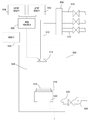
도 5는 개시된 실시예들에 따른 증착 프로세스 및/또는 플라즈마 처리 프로세스에 적합한 프로세싱 챔버의 개략적인 예시이다.
도 6은 개시된 실시예들에 따른 증착 프로세스들에 적합한 프로세싱 장치의 개략적인 예시이다.
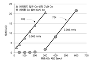
도 7 및 도 8은 개시된 실시예들에 따라 코발트를 증착한 것으로부터의 실험적 결과들을 도시하는 플롯들이다.
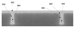
도 9a는 코발트로 충진된 피처들의 SEM 화상이다.
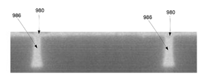
도 9b는 개시된 실시예들에 따라 코발트로 충진된 피처들의 SEM 화상이다.Figures 1A-1C are schematic illustrations of cobalt filling in features.
2 is a process flow diagram illustrating a method according to the disclosed embodiments.
Figures 3A-3G are schematic illustrations of filled features using cobalt in accordance with the disclosed embodiments.
Figures 4A-4H are schematic illustrations of filled features using cobalt in accordance with the disclosed embodiments.
5 is a schematic illustration of a processing chamber suitable for a deposition process and / or a plasma processing process according to the disclosed embodiments.
Figure 6 is a schematic illustration of a processing device suitable for deposition processes according to the disclosed embodiments.
Figures 7 and 8 are plots showing experimental results from depositing cobalt in accordance with the disclosed embodiments.
9A is a SEM image of features filled with cobalt.
Figure 9b is an SEM image of features filled with cobalt in accordance with the disclosed embodiments.
이하의 기술에서, 제시된 실시예들의 전체적인 이해를 제공하기 위해 다수의 구체적인 상세들이 언급된다. 개시된 실시예들은 이들 구체적인 상세들 일부 또는 전부가 없이도 실시될 수도 있다. 다른 예들에서, 공지의 프로세스 동작들은 개시된 실시예들을 불필요하게 모호하게 하지 않도록 상세히 기술되지 않았다. 개시된 실시예들이 구체적인 실시예들과 함께 기술되지만, 이는 개시된 실시예들로 제한하도록 의도되지 않는다는 것이 이해될 것이다.In the following description, numerous specific details are set forth in order to provide a thorough understanding of the disclosed embodiments. The disclosed embodiments may be practiced without some or all of these specific details. In other instances, well-known process operations have not been described in detail so as not to unnecessarily obscure the disclosed embodiments. While the disclosed embodiments are described in conjunction with specific embodiments, it will be understood that they are not intended to be limited to the disclosed embodiments.
반도체 제조 시, 피처들은 도전성 재료들로 충진될 수도 있다. 예를 들어, FEOL (front end of line) 애플리케이션들에서와 같이, 콘택트들을 형성하기 위해 종종 텅스텐이 피처들 내에 충진된다.In semiconductor fabrication, features may be filled with conductive materials. For example, as in front end of line (FEOL) applications, tungsten is often filled into features to form contacts.
그러나, 디바이스들을 축소됨에 따라, 종횡비들은 상승하고 보다 작은 피처들이 콘택트들을 형성하기 위해 사용된다. 많은 애플리케이션들에서, 코발트와 같은, 대안적인 도전성 재료가 콘택트들을 형성하거나 그렇지 않으면 피처들을 충진하도록 사용될 수도 있다.However, as the devices are shrunk, the aspect ratios rise and smaller features are used to form the contacts. In many applications, alternative conductive materials, such as cobalt, may be used to form contacts or otherwise fill features.
반도체 제조시 종래의 코발트 증착은 전기도금을 포함하였다. 코발트 전기 도금 시, 금속이 충분히 도전성이 되도록, 금속의 일부 두께가 먼저 피처 내에 증착되고, 이는 전기도금 프로세스에서 전류가 피처 내의 금속의 성장을 허용하게 한다. 이러한 씨드층들은 확실히 최대 저항을 가질 수도 있다. 전기도금과 같은 습식 기반 코발트 피처 충진 프로세스들은 통상적으로 씨드층의 증착과는 상이한 툴에서의 피처 충진을 수반하여, 프로세스의 복잡성 및 제작 비용을 증가시킨다.Conventional cobalt deposition during semiconductor manufacturing involved electroplating. During cobalt electroplating, some thickness of the metal is first deposited in the feature such that the metal is sufficiently conductive that current in the electroplating process allows the growth of the metal in the feature. These seed layers may certainly have maximum resistance. Wet-based cobalt feature fill processes, such as electroplating, typically involve the filling of features in a tool that is different from the deposition of a seed layer, thereby increasing process complexity and manufacturing costs.
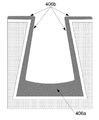
코발트는 또한 원자층 증착 (ALD: atomic layer deposition) 또는 화학적 기상 증착 (CVD: chemical vapor deposition) 에 의해 증착될 수도 있다. 종래의 ALD 또는 CVD에서, 보이드들은 피처 프로파일로 인해 피처들 내에 형성될 수도 있다. 도 1a는 기판 (102) 내의 이러한 피처 (100) 의 예의 개략적인 예시이다. 기판은, 그 위에 증착된 유전체, 도전성, 또는 반도전성 재료와 같은 재료의 하나 이상의 층들을 갖는 웨이퍼를 포함하는, 실리콘 웨이퍼, 예를 들어, 200-㎜ 웨이퍼, 300-㎜ 웨이퍼, 또는 450-㎜ 웨이퍼일 수도 있다. 피처들은 하나 이상의 좁은 및/또는 재차 들어간 개구부들, 피처들 내에서의 협착 (constriction), 및 고 종횡비를 특징으로 할 수 있다. 일부 실시예들에서, 피처 (100) 는 적어도 약 2:1, 적어도 약 10:1, 적어도 약 15:1, 적어도 약 20:1 이상의 종횡비를 가질 수도 있다. 피처 홀 (105) 은 또한 개구부 근방의 치수, 예를 들어, 약 19 ㎚ 미만의 개구부 직경, 또는 라인 폭, 또는 개구부 폭, 또는 임계 치수를 가질 수도 있고, 또한 1x ㎚ 미만의 피처 폭들로 공지된다. 피처 (100) 는 충진되지 않은 피처 또는 단순히 피처로 지칭될 수 있다. 피처, 및 임의의 피처는, 수직 축들을 갖는 수직으로 배향된 피처들 및 수평 축들을 갖는 수평으로 배향된 피처들을 갖는, 피처의 길이를 따라 연장하는 축을 부분적으로 특징으로 할 수도 있다.Cobalt may also be deposited by atomic layer deposition (ALD) or chemical vapor deposition (CVD). In conventional ALD or CVD, the voids may be formed in the features due to the feature profile. 1A is a schematic illustration of an example of such a
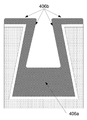
도시된 바와 같이, 기판 (102) 은 피처의 하단부의 폭보다 좁은 피처 개구부 (110) 를 갖는 피처 (100) 를 포함한다. 도 1a의 피처 (100) 는 재차 들어간 프로파일을 포함한다. 재차 들어간 프로파일은 피처의 하단부, 폐쇄된 단부, 또는 내부로부터 피처 개구부로 좁아지는 프로파일이다. 다양한 실시예들에 따라, 프로파일은 점진적으로 좁아질 수도 있고/있거나 피처 개구부에서 오버행을 포함할 수도 있다. 도 1a에 도시된 재차 들어간 패턴은, 확산 배리어의 증착과 같은, 이전의 막 증착에서 컨포멀하지 않은 막 단차 커버리지로 인해 패터닝 및/또는 오버행 동안 비대칭적인 에칭 동역학에 의해 생성될 수도 있다. 다양한 예들에서, 피처는 피처의 하단부의 폭보다 피처의 상단부에서 개구부의 보다 좁은 폭을 가질 수도 있다. 도 1b는 피처 (100) 내로 컨포멀하게 증착된 배리어층 (104) 의 개략적인 예시이다. 배리어층 (104) 이 증착된 후, ALD 또는 CVD에 의한 종래의 코발트 증착은 피처 (100) 내에 컨포멀한 막을 형성하였다. 도 1c는 종래의 ALD 또는 CVD 방법들에 의해 코발트 (106) 를 사용하여 충진된 피처 (100) 의 개략적인 예시이다. 컨포멀한 단차 커버리지로 인해, 코발트 막 (106) 은 재차 들어간 패턴 입구 내에 핀치-오프 (pinch-off) 를 갖고 피처 (100) 의 패턴 내에 보이드 (160) 의 형성을 발생시킨다. 코발트 핀치-오프는 코발트 갭 충진 전에도 재차 들어간 패턴 상에서 발생될 수도 있어서, 피처 (100) 를 폐쇄하고 보이드 (160) 를 형성한다. 보이드는 충진되지 않고 남겨진 피처 내의 영역이다. 보이드는, 예를 들어, 증착된 재료가 피처 내에 핀치 지점을 형성할 때 반응 물질 진입 및 증착을 방지하는, 피처 내의 충진되지 않은 공간의 시일링부를 형성할 수 있다. 피처들 내의 보이드들의 형성은 종종 디바이스 고장을 발생시킨다.As shown, the
큰 종횡비를 갖는 피처들을 포함하여, 작은 피처 및 큰 피처들 모두에 보이드-프리 (void-free) 코발트를 증착하는 방법은 패시베이션 처리에 의해 수행되고, 본 명세서에 제공된다. 본 명세서에 기술된 방법들은, 앞선 막 증착 또는 에칭으로부터 발생할 수도 있는, 재차 들어간 구조들 및/또는 오버행들을 갖는 좁게 패터닝된 기판들에 적용가능하다. 방법들은, 처리된 코발트 표면 및 처리되지 않은 코발트 표면에 대한 코발트 막 성장 동역학에 기초하여 코발트 막 성장 프로파일을 성형하기 위해, 코발트 표면의 일부 양태들에서 코발트 막 성장을 선택적으로 억제하기 위한 처리를 사용하는 것을 수반한다. 처리된 표면들은 보다 긴 핵생성 지연들을 나타내고, 이는 보텀-업 충진 프로세스에서 처리되지 않은 표면들로부터의 성장을 허용한다. 이러한 방법들은 BEOL (back end of line) 프로세스들에서의 비아/라인 충진뿐만 아니라, FEOL (front end of line) 프로세스들에서의 금속 게이트의 제조/콘택트 충진에 적용가능할 수도 있다. 종합적으로, 본 명세서에 기술된 증착 기법들은 보이드-프리 코발트 충진된 피처들을 발생시킨다.A method for depositing void-free cobalt on both small and large features, including features with large aspect ratios, is performed by a passivation process and is provided herein. The methods described herein are applicable to narrowly patterned substrates having recessed structures and / or overhangs that may arise from previous film deposition or etching. The methods use a process to selectively inhibit cobalt film growth in some aspects of the cobalt surface to form a cobalt film growth profile based on the cobalt film growth kinetics for the treated and untreated cobalt surfaces Lt; / RTI > The treated surfaces exhibit longer nucleation delays, which allows growth from untreated surfaces in a bottom-up filling process. These methods may be applicable to fabrication / contact filling of metal gates in front end of line (FEOL) processes, as well as via / line filling in back end of line (BEOL) processes. Collectively, the deposition techniques described herein generate void-free cobalt-filled features.
방법들은 단일 처리를 사용하여, 또는 복수의 사이클들의 처리를 사용하여 피처들을 충진하는 것을 포함한다. 단일 처리 방법은 약 3x ㎚ 미만 또는 약 1x ㎚ 미만 (예를 들어, 약 19 ㎚ 미만) 폭의 단위의 개구부를 갖는 피처들과 같은, 보다 작은 피처들에 대해 사용될 수도 있다. 다양한 실시예들에서, 단일 처리 방법은 적어도 약 1.5:1 이상, 또는 약 10:1 이상의 종횡비를 갖는 피처들 내에 코발트를 증착하기 위해 사용된다. 복수의 처리 방법은 약 2x ㎚, 3x ㎚, 또는 4x ㎚보다 큰 단위의 개구부를 갖는, 보다 큰 피처들에 대해 사용될 수도 있다. 복수의 처리들에서, 사이클 각각은 마지막 사이클까지 피처의 남아 있는 개구부를 감소시킨다. 도면들에 대하여 실시예들이 개시된다.The methods include filling the features using a single process, or using a plurality of cycles of processing. The single processing method may be used for smaller features, such as features having openings in the unit of width less than about 3 x nm or less than about 1 x nm (e.g., less than about 19 nm). In various embodiments, the single processing method is used to deposit cobalt within features having an aspect ratio of at least about 1.5: 1 or more, or about 10: 1 or more. A plurality of processing methods may be used for larger features having openings in the unit of greater than about 2 x nm, 3 x nm, or 4 x nm. In a plurality of processes, each cycle reduces the remaining openings of the feature up to the last cycle. Embodiments are disclosed with respect to the figures.
도 2는 개시된 실시예들에 따른 방법들을 수행하기 위한 동작들의 프로세스 흐름도이다. 동작 202에서, 충진될 피처를 갖는 기판이 제공된다. 기판은 실리콘 기판일 수도 있고 또는 또 다른 적합한 반도체 기판일 수도 있다. 기판은 하나보다 많은 피처를 포함할 수도 있고, 그리고 다양한 사이즈들을 갖는 피처들을 갖는 피처들의 패턴 또는 일 사이즈의 피처들을 포함할 수도 있다. 기술을 목적으로, 도 2는 단일 피처의 충진의 맥락에서 논의되지만, 다양한 사이즈들의 피처들이 또한 유사하게 충진될 수도 있다는 것이 이해될 것이다. 피처들은 상기 기술된 임의의 피처들일 수도 있다.2 is a process flow diagram of operations for performing the methods according to the disclosed embodiments. At
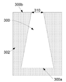
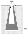
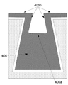
도 3a는 기판 (302) 내의 작은 피처 (300) 의 예를 제공한다. 작은 피처 (300) 는 작은 피처 (300) 의 하단부 (300a) 보다 좁은, 작은 피처 (300) 의 상단부 (300b) 에서 좁은 피처 개구부 (310) 를 포함한다.Figure 3A provides an example of a
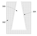
동작 204a에서, 배리어 막 또는 배리어층이 기판 상에 선택적으로 증착된다. 다양한 실시예들에서, 배리어 막은 컨포멀하게 증착된다. 배리어 막은 텅스텐 나이트라이드 (WN), 티타늄 나이트라이드 (TiN), 또는 임의의 적합한 배리어 막의 박층일 수도 있다. 배리어 막들의 추가적인 예들은 텅스텐 (W), 티타늄 (Ti), 탄탈룸 (Ta), 탄탈룸 나이트라이드 (TaN), 코발트 나이트라이드 (CoN), 및 루테늄 (Ru) 를 포함한다. 다양한 실시예들에서, 배리어 막은 ALD 방법 또는 CVD 방법에 의해 증착된다. 배리어 막은, 배리어 막 재료 및 코발트가 강하고, 높은 접착 에너지 계면을 형성하도록, 선택될 수도 있다. 도 3b는 작은 피처 (300) 내에 증착된 배리어 막 (304) 의 예를 제공한다. 도시된 바와 같이, 배리어 막 (304) 은 피처 내에 컨포멀하게 증착되어, 피처 (300) 의 윤곽을 따라 기판 (302) 상에 얇은 배리어를 형성한다.In
일부 실시예들에서, 204a 후에, 배리어 막은 동작 204b에서 질소계 플라즈마를 사용하여 선택적으로 처리될 수도 있다. 처리는 후속하는 동작들에서 코발트 핵생성을 억제하도록 수행될 수도 있다. 예를 들어, 처리는 동작 212에서 벌크 코발트 충진을 억제하도록 수행된다. 일부 실시예들에서, 처리는 동작 206에서 벌크 코발트 충진을 억제한다. 처리 프로세스 조건들은 동작 208에 대하여 이하에 더 기술된다. 일부 실시예들에서, 배리어 막은, 피처 개구부가 약 1x ㎚ 이하의 단위라면 처리된다.In some embodiments, after 204a, the barrier film may optionally be treated using nitrogen-based plasma in
동작 204c에서, 남아 있는 피처 개구부가 충분히 작은지 여부가 결정된다. 약 1 ㎚ 미만의 피처 개구부들을 갖는 실시예들에서, 배리어 막이 동작 204a에서 증착되고 표면이 204b에서 처리된 후, 피처 개구부는 충분히 작을 수도 있다. 피처 개구부가 충분히 작은지 여부에 대한 결정을 위한 고려 사항들은 동작 210에 대하여 이하에 기술된다. 일반적으로, 증착하는 피처 개구부가 너무 작으면, 피처 내부로의 코발트 씨드층은 피처 개구부를 좁게 하고 벌크 코발트 충진 프로세스들을 방지하거나 감소시키고, 피처 개구부는, 이하에 더 기술될 바와 같이, 동작 212에서 피처 내부로 벌크 코발트를 바로 증착하도록 충분히 작다. 피처가 충분히 작지 않으면, 동작 206이 수행된다.In
동작 206에서, 피처는 저온에서 코발트로 부분적으로 충진된다. 다양한 실시예들에서, 이 부분 충진은 "씨드층"으로 지칭될 수도 있다. 피처는 코발트 함유 전구체 및 환원제에 기판을 노출시킴으로써 부분적으로 충진된다. 동작 206은 코발트가 증착되는 동안 플라즈마가 생성되지 않거나 챔버로 도입되지 않도록 열적으로 수행될 수도 있다.At 206, the feature is partially filled with cobalt at low temperature. In various embodiments, this partial filling may be referred to as a "seed layer ". The features are partially filled by exposing the substrate to a cobalt-containing precursor and a reducing agent.
코발트는 ALD 또는 CVD 방법들에 의해 피처 내에 컨포멀하게 증착될 수도 있다. CVD 방법에서, 기판은 기판 상에 코발트층을 형성하기 위해 적합한 코발트 함유 전구체 및 환원제에 노출된다. 온도는 약 70 ℃ 내지 약 400 ℃, 또는 약 80 ℃ 내지 약 200 ℃일 수도 있다. 일부 실시예들에서, 온도는 약 70 ℃ 내지 약 200 ℃, 또는 약 100 ℃ 내지 약 120 ℃일 수도 있다. 챔버 압력은 약 0.1 Torr 내지 약 10 Torr, 또는 약 1 Torr 내지 약 5 Torr일 수도 있다. 일부 실시예들에서, 챔버 압력은 약 0.5 Torr 내지 약 10 Torr, 또는 약 1 Torr 내지 약 3 Torr일 수도 있다. 다양한 실시예들에서, 적합한 코발트 함유 전구체 및/또는 환원제 아르곤 (Ar), 질소 (N2), 또는 이산화탄소 (CO) 와 같은 캐리어 가스를 사용하여 챔버 내로 도입된다. 일부 실시예들에서, 코발트 함유 전구체는 캐리어 가스로서 아르곤을 사용하여 챔버로 도입된다. 캐리어 가스의 플로우 레이트는 약 10 sccm 내지 약 300 sccm, 또는 약 10 sccm 내지 약 50 sccm일 수도 있다. 일부 실시예들에서, 캐리어 가스의 플로우 레이트는 약 10 sccm 내지 약 100 sccm, 또는 약 10 sccm 내지 약 30 sccm일 수도 있다. 환원제는 선택된 코발트 함유 전구체를 환원시키기 위한 임의의 적합한 반응 물질일 수도 있다. 다양한 실시예들에서, 환원제는 수소 (H2) 이다. 환원제는 약 100 sccm 내지 약 5000 sccm, 또는 약 2000 sccm 내지 약 5000 sccm으로 도입될 수도 있다. 특정한 증착 챔버에 따라, 본 개시 전체에 제공된 범위들 밖의 플로우 레이트들이 사용될 수도 있다는 것이 이해될 것이다.Cobalt may be conformally deposited in the feature by ALD or CVD methods. In the CVD process, the substrate is exposed to a cobalt-containing precursor and a reducing agent suitable for forming a cobalt layer on the substrate. The temperature may be from about 70 캜 to about 400 캜, or from about 80 캜 to about 200 캜. In some embodiments, the temperature may be from about 70 캜 to about 200 캜, or from about 100 캜 to about 120 캜. The chamber pressure may be from about 0.1 Torr to about 10 Torr, or from about 1 Torr to about 5 Torr. In some embodiments, the chamber pressure may be from about 0.5 Torr to about 10 Torr, or from about 1 Torr to about 3 Torr. In various embodiments, suitable cobalt-containing precursors and / or reducing agents are introduced into the chamber using a carrier gas such as argon (Ar), nitrogen (N 2 ), or carbon dioxide (CO). In some embodiments, the cobalt-containing precursor is introduced into the chamber using argon as the carrier gas. The flow rate of the carrier gas may be between about 10 sccm and about 300 sccm, or between about 10 sccm and about 50 sccm. In some embodiments, the flow rate of the carrier gas may be between about 10 sccm and about 100 sccm, or between about 10 sccm and about 30 sccm. The reducing agent may be any suitable reactant for reducing the selected cobalt-containing precursor. In various embodiments, the reducing agent is hydrogen (H 2 ). The reducing agent may be introduced at from about 100 sccm to about 5000 sccm, or from about 2000 sccm to about 5000 sccm. It will be appreciated that, depending on the particular deposition chamber, flow rates outside the ranges provided throughout this disclosure may be used.
ALD 방법에서, 기판은, 기판이 먼저 적합한 코발트 함유 전구체에 노출되고, 이어서 전구체가 퍼지되고, 이어서 기판이 환원제의 펄스에 노출되고, 그리고 이어서 환원제가 퍼지되는 사이크들에 노출될 수도 있고, 이러한 사이클들은 목표된 두께의 코발트가 기판 상에 형성될 때까지 반복될 수도 있다. ALD에 의한 증착 프로세스를 위해, 온도는 약 70 ℃ 내지 약 400 ℃, 또는 약 100 ℃ 내지 약 200 ℃일 수도 있다. 일부 실시예들에서, 온도는 약 70 ℃ 내지 약 200 ℃, 또는 약 100 ℃ 내지 약 120 ℃일 수도 있다. 압력은 약 1 Torr 내지 약 20 Torr, 또는 약 8 Torr 내지 약 15 Torr일 수도 있다. 다양한 실시예들에서, 코발트 함유 전구체 및/또는 환원제는 Ar, N2, 또는 CO와 같은 캐리어 가스를 사용하여 챔버 내로 도입된다. 일부 실시예들에서, 코발트 함유 전구체는 캐리어 가스로서 Ar을 사용하여 챔버로 도입된다. 캐리어 가스의 플로우 레이트는 약 10 sccm 내지 약 300 sccm, 또는 약 10 sccm 내지 약 100 sccm일 수도 있다. 일부 실시예들에서, 캐리어 가스의 플로우 레이트는 약 50 sccm 내지 약 100 sccm일 수도 있다. 환원제는 코발트 함유 전구체를 환원시키기 위한 임의의 적합한 반응 물질일 수도 있다. 다양한 실시예들에서, 환원제는 H2이다. 환원제는 약 100 sccm 내지 약 5000 sccm, 또는 약 2000 sccm 내지 약 5000 sccm의 플로우 레이트로 도입될 수도 있다. 동작 206이 종료되는 시간은 피처의 크기에 따른다.In the ALD process, the substrate may be exposed to a cycle in which the substrate is first exposed to a suitable cobalt-containing precursor, then the precursor is purged, then the substrate is exposed to pulses of a reducing agent, and then the reducing agent is purged, May be repeated until the desired thickness of cobalt is formed on the substrate. For a deposition process by ALD, the temperature may be from about 70 캜 to about 400 캜, or from about 100 캜 to about 200 캜. In some embodiments, the temperature may be from about 70 캜 to about 200 캜, or from about 100 캜 to about 120 캜. The pressure may be from about 1 Torr to about 20 Torr, or from about 8 Torr to about 15 Torr. In various embodiments, the cobalt-containing precursor and / or reducing agent is introduced into the chamber using a carrier gas such as Ar, N 2 , or CO. In some embodiments, the cobalt-containing precursor is introduced into the chamber using Ar as a carrier gas. The flow rate of the carrier gas may be between about 10 sccm and about 300 sccm, or between about 10 sccm and about 100 sccm. In some embodiments, the flow rate of the carrier gas may be between about 50 sccm and about 100 sccm. The reducing agent may be any suitable reactant for reducing the cobalt-containing precursor. In various embodiments, the reducing agent is H 2 . The reducing agent may be introduced at a flow rate of from about 100 sccm to about 5000 sccm, or from about 2000 sccm to about 5000 sccm. The time at which
예시적인 코발트 함유 전구체들은 디카르보닐 사이클로펜타디에닐 코발트 (I), 코발트 카르보닐, 다양한 코발트 아미디네이트 전구체들, 코발트 디아자디에닐 착체들, 코발트 아미디네이트/구아니디네이트 전구체들, 및 이들의 조합들을 포함한다. 적합한 코발트 함유 전구체들은 유기기들 및/또는 카르보닐기들을 갖는 코발트 중심을 포함할 수도 있고, 여기서 유기기들은, 직쇄 또는 분지쇄 (branched chains) 탄화수소일 수도 있는, 메틸, 에틸, 프로필, 부틸, 펜틸, 헥실, 헵틸, 및 옥틸과 같은 알킬들을 포함한다. 일부 실시예들에서, 유기금속성 화합물은 치환되거나 치환되지 않은 아릴 리간드를 갖는다. 일부 실시예들에서, 아릴 리간드는 치환되지 않는다.Exemplary cobalt-containing precursors include dicarbonyl cyclopentadienyl cobalt (I), cobalt carbonyl, various cobalt amidinate precursors, cobalt diazadienyl complexes, cobalt amidinate / guanidinate precursors, And combinations thereof. Suitable cobalt containing precursors may include cobalt centers with organic groups and / or carbonyl groups wherein the organic groups are selected from the group consisting of methyl, ethyl, propyl, butyl, pentyl, isobutyl, sec-butyl, Hexyl, heptyl, and octyl. In some embodiments, the organometallic compound has a substituted or unsubstituted aryl ligand. In some embodiments, the aryl ligand is not substituted.
일부 실시예들에서 유기금속성 코발트 화합물은 다음의 구조를 갖는다:In some embodiments, the organometallic cobalt compound has the structure:

여기서 R1은 C1-C8-알킬, R2는 C1-C8 알킬, x는 0, 1 또는 2이고; y는 0 또는 1이다.Wherein R 1 is C 1 -C 8 -alkyl, R 2 is C 1 -C 8 alkyl, x is 0, 1 or 2; y is 0 or 1;
일부 실시예들에서 R1은 C2-C8-알킬, R2는 별도의 C2-C8 알킬이다.In some embodiments, R 1 is C 2 -C 8 -alkyl and R 2 is a separate C 2 -C 8 alkyl.
본 명세서에서 사용된 바와 같이, 용어 "알킬"은 메틸, 에틸, 프로필, 부틸, 펜틸, 헥실, 헵틸, 및 옥틸과 같이 길이에 있어서, 1 내지 8 개의 원자들의 포화된 탄화수소 체인을 지칭한다. 용어 "알킬"은 직쇄 및 분지쇄 탄화수소 모두를 포함한다. 따라서, 용어 프로필은 프로필은 n-프로필 및 이소프로필을 모두 포함한다. 용어 부틸은 n-부틸, sec-부틸, iso-부틸, 및 tert-부틸을 모두 포함한다.As used herein, the term "alkyl" refers to a saturated hydrocarbon chain of 1 to 8 atoms in length, such as methyl, ethyl, propyl, butyl, pentyl, hexyl, heptyl, and octyl. The term "alkyl" includes both straight and branched chain hydrocarbons. Thus, the term profile includes both n - propyl and isopropyl. The term butyl includes both n-butyl, sec -butyl, iso -butyl, and tert -butyl.
일부 실시예들에서 x는 0이고 y는 1이다. 본 실시에에 따른 유기금속성 화합물은 이하에 도시된다:In some embodiments, x is 0 and y is 1. The organometallic compounds according to this embodiment are shown below:

특정한 기술된 화합물들은 캘리포니아, 프레몬트의 Lam Research Inc.로부터 상업적으로 입수가능한 대응하는 증착 장치들과 함께, 메사추세츠, 하버힐의 SAFC-Hitech로부터 상업적으로 입수가능하다.Certain described compounds are commercially available from SAFC-Hitech, Harbor Hill, MA, with corresponding deposition devices commercially available from Lam Research Inc. of Fremont, California.
일부 실시예들에서, 코발트 함유 전구체는 약 100 ℃ 미만의 온도에서와 같이, 저온에서 고 증기압을 갖는 금속-유기 전구체들을 포함한다. 예시적인 증기압은 약 30 ℃ 분위기에서 약 0.5 Torr일 수도 있다. 이러한 전구체들은, 이하에 기술된, 나중의 코발트 증착이 처리되지 않은 표면 또는 처리된 표면에 대해 선택적이 되도록, 매우 선택적이다. 예를 들어, 코발트 함유 전구체는 이하에 기술될 바와 같이, 처리되지 않은 표면들에 비해 처리된 표면들 상에서 충분한 핵생성 지연을 생성하도록 성장 선택도를 가질 수도 있다. 예를 들어, 핵생성 지연은 약 200 초를 초과할 수도 있다.In some embodiments, the cobalt-containing precursor comprises metal-organic precursors having a high vapor pressure at a low temperature, such as at a temperature less than about 100 < 0 > C. Exemplary vapor pressures may be about 0.5 Torr in an atmosphere of about 30 < 0 > C. These precursors are highly selective so that later cobalt deposition, described below, is selective for untreated or treated surfaces. For example, a cobalt-containing precursor may have growth selectivity to produce sufficient nucleation delay on treated surfaces as compared to untreated surfaces, as described below. For example, the nucleation delay may exceed about 200 seconds.
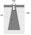
도 3c는 배리어층 (304) 위의 작은 피처 (300) 내에 부분적으로 충진된 코발트 씨드층 (306) 의 개략적인 예시이다. 코발트 씨드층 (306) 이 또한 컨포멀하다는 것을 주의한다. 작은 피처 (300) 는, 피처의 상단에서의 개구부가 후속하는 프로세싱에서 약간의 플라즈마가 들어가게 하도록 충분히 작고, 피처의 측벽들 대부분으로 플라즈마가 들어가는 것을 방지하기에 충분히 작을 때 피처 (300) 의 충진이 종료되도록 부분적으로 충진된다. 피처의 상단부에 남아 있는 개구부는 후속하는 프로세싱에서 플라즈마가 들어가게 하지만, 306b로 나타낸 바와 같이 증착된 코발트의 측벽들의 상단 약 10 내지 30 %까지의 플라즈마 노출을 제한하도록 준비되고, 이는 이하에 상세히 논의된다.3C is a schematic illustration of a partially filled
약 3x ㎚보다 크거나, 약 1x ㎚보다 큰 최초의 개구부를 갖는 피처와 같이, 피처가 큰 피처이면, 피처 상에 남아 있는 개구부가 피처의 측벽들 대부분으로 플라즈마가 들어가는 것을 방지하기에 충분히 작지 않아도, 미리 결정된 시간에 부분적인 충진이 정지된다.If the feature is a large feature, such as a feature having an initial opening greater than about 3 x nm, or greater than about 1 x nm, then the opening remaining on the feature is not small enough to prevent plasma from entering the majority of the sidewalls of the feature , Partial filling stops at a predetermined time.
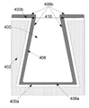
도 4a는 기판 (402) 내의 큰 피처 (400) 의 예의 개략적인 예시이다. 큰 피처 (400) 는, 약 2x ㎚ 또는 약 3x ㎚보다 큰 단위일 수도 있는 피처 개구부 (410) 를 갖는다. 큰 피처 (400) 는 도 2에 대하여 상기에 기술된 동작 204에 따라 컨포멀하게 증착된, 선택적인 배리어 막 (404) 을 포함한다. 코발트 씨드층 (406) 은 도 2에 대하여 동작 206 마다 기판 위에 컨포멀하게 증착되고, 코발트 씨드층 증착을 종료하기 위해 미리 결정된 시간은 피처 크기에 따른다.FIG. 4A is a schematic illustration of an example of a
도 2로 돌아가면, 동작 208에서 피처의 상단에서 그리고 상단 근방에서의 코발트 표면들은 질소 함유 가스로부터 생성된 플라즈마에 노출시킴으로써 처리된다. 이러한 처리는 "ICE (inhibitor controlled exposure)" 또는 "플라즈마 기반 표면 질화"라고 할 수도 있다. 다양한 실시예들에서, 플라즈마는, 플라즈마로부터의 활성 종이 기판의 평면에 수직인 방향으로 피처의 표면들에 직접적으로 접하도록, 지향성 플라즈마이다. 일부 실시예들에서, 처리된 표면들은, 후속하는 프로세싱에서 긴 핵생성 지연을 트리거하는, 코발트 나이트라이드 (CoNx) 를 형성할 수도 있다. 동작 204b에서 처리된 것과 같은, 처리된 배리어 막은 처리된 코발트 막에 대한 핵생성 지연보다 짧은 핵생성 지연을 가질 수도 있다. 이하의 기술은 처리된 코발트 표면들을 기술하지만, 임의의 이하의 처리 프로세스들 및 조건들은 동작 204b에서와 같이, 배리어 막들을 처리하고, 처리된 배리어 막을 형성하기 위해 사용될 수도 있다는 것이 이해될 것이다.Returning to FIG. 2, in
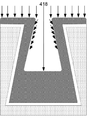
다양한 피처들이 피처의 하단부의 폭보다 좁은 개구부를 가질 수도 있기 때문에, 플라즈마는 대부분 피처의 상단 표면들 및 피처 측벽의 상단 약 10 % 내지 약 50 %를 처리한다. 일부 실시예들에서, 플라즈마는 피처 측벽들의 상단 약 10 % 내지 약 30 %를 처리한다. 작은 피처를 수반하는 다양한 실시예들에서, 좁은 개구부로 인해, 측벽들의 하단 약 50 % 내지 90 %는 처리되지 않고 남는다. 일부 실시예들에서, 측벽들의 하단 약 70 % 내지 90 %는 처리되지 않고 남는다. 일부 실시예들에서, 활성 종이 피처 개구부를 때릴 때 (hit), 질소 이온들은 개구부 주변에 충돌하고, 피처의 상단 근방에 작은 구배 (gradient) 의 처리된 코발트 표면들을 남긴다. 처리된 표면들이 보다 긴 핵생성 지연을 나타내기 때문에, 코발트 핵생성은, 차동 억제 프로파일이 처리에 의해 형성된 피처 축을 따르도록, 처리된 표면들 상에서 선택적으로 억제된다. 선택적인 패시베이션, 차동 억제, 또는 차동 패시베이션으로 또한 지칭될 수도 있는, 선택적인 억제는 피처의 일부분들 상에서 후속하는 코발트 핵생성 억제를 수반하지만, 피처의 나머지들에서 핵생성을 억제하지 않는다 (또는 보다 적은 정도로 핵생성을 억제한다). 예를 들어, 일부 실시예들에서, 피처는 피처 개구부에서 또는 피처 개구부 근방 (예를 들어, 피처 측벽들의 상단 약 10 % 내지 약 50 %, 또는 약 10 % 내지 약 30 % 및 피처의 상단 표면들) 에서 선택적으로 억제되지만, 피처 내부 측벽들의 하단 약 70 % 내지 90 %, 또는 약 50 % 내지 90 %에서의 핵생성은 억제되지 않는다.Because the various features may have openings that are narrower than the width of the bottom of the features, the plasma handles about 10% to about 50% of the top of most features and the top of the feature sidewalls. In some embodiments, the plasma processes about 10% to about 30% of the top of the feature sidewalls. In various embodiments involving small features, due to the narrow openings, about 50% to 90% of the bottom of the sidewalls remain untreated. In some embodiments, about 70% to about 90% of the bottom of the sidewalls remains untreated. In some embodiments, when hitting the active paper feature opening (hit), the nitrogen ions collide around the aperture and leave a small gradient of processed cobalt surfaces near the top of the feature. Since the treated surfaces exhibit longer nucleation delays, the cobalt nucleation is selectively inhibited on the treated surfaces such that the differential inhibition profile follows the feature axis formed by the treatment. A selective inhibition, which may also be referred to as selective passivation, differential suppression, or differential passivation, involves subsequent cobalt nucleation inhibition on portions of the feature, but does not inhibit nucleation in the remainder of the feature To a lesser extent inhibiting nucleation). For example, in some embodiments, the features may be located at or near the feature openings (e.g., between about 10% and about 50%, or between about 10% and about 30% of the top of the feature sidewalls, ), But nucleation at about 70% to 90%, or about 50% to 90%, of the bottom of the feature inner sidewalls is not inhibited.
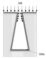
도 3d는 증착된 코발트 (306) 의 표면들에 지향된 플라즈마로부터 생성된 질소 이온들 (308) 의 개략적인 예시이다. 피처의 상단부 (306b) 에서 코발트의 표면들은 질소 이온들 (308) 에 노출되지만, 피처의 하단부 (306a) 에서 코발트의 표면들은 질소 이온들에 노출되지 않는다는 것을 주의한다. 피처 (300) 의 상단부에서 보다 좁은 개구부로 인해, 질소 이온들이 측벽들의 상단 약 10 내지 50 %를 때리도록, 처리된 코발트 표면들 (306b) 의 차동 억제 프로파일 형성한다. 측벽들 상의 화살표들은 피처의 개구부 주변에서 질소 이온들의 충돌을 도시하기 위해 도시되었다는 것을 주의한다.FIG. 3D is a schematic illustration of
큰 피처가 코발트로 충진되는 실시예들에서, 질소 이온들이 전체 피처에 들어가고 피처의 하단부 일부 및 측벽들의 하단부 일부분들을 처리할 수도 있다. 그러나, 피처의 형상으로 인해, 피처 측벽들의 상단 일부분은 피처의 하단 측벽들보다 보다 많은 질소 이온들로 처리될 수도 있다.In embodiments where the large feature is filled with cobalt, nitrogen ions may enter the entire feature and process a portion of the bottom of the feature and a portion of the bottom of the sidewalls. However, due to the shape of the features, the upper portion of the feature sidewalls may be treated with more nitrogen ions than the lower sidewalls of the feature.
도 4b는 플라즈마 및 질소 이온들 (408) 에 노출된 코발트 씨드층 (406) 을 갖는 보다 큰 피처 (400) 의 개략적인 예시이다. 도 3d와 비교하여, 피처 하단부 (400a) 는 또한 보다 넓은 개구부로 인해 플라즈마에 노출된다는 것을 주의한다. 그러나, 표면이 플라즈마 (308) 로부터 더 이격되기 때문에, 하단부 (400a) 에서의 표면은 측벽들 또는 피처의 상단부에서의 표면들만큼 플라즈마 (308) 에 노출되지 않을 수도 있다.FIG. 4B is a schematic illustration of a
동작 208에서 수행된 처리는 약 400 ℃ 미만, 또는 약 50 ℃ 내지 약 200 ℃, 또는 약 70 ℃ 내지 약 200 ℃의 온도로 수행될 수도 있다. 챔버 압력은 약 10 Torr 미만, 또는 약 0.1 Torr 내지 약 5 Torr, 또는 약 0.5 Torr 내지 약 2 Torr일 수도 있다. 사용된 플라즈마는 바이어스를 갖는 지향성 인 시추 플라즈마일 수도 있다. 필수적인 것은 아니지만 통상적으로, 이러한 플라즈마는 용량 결합된다. 대안적으로, 유도 결합일 수도 있다. 단일 스테이션에 대한 플라즈마 전력은 약 50 W 내지 약 5000 W, 또는 100 W 내지 약 1000 W, 또는 약 100 W 내지 약 500 W, 또는 약 200 W 내지 약 500 W일 수도 있다. 플라즈마를 생성하기 위해 챔버에 도입된 가스는 임의의 질소 함유 가스 또는 질소 함유 가스들의 혼합물일 수도 있다. 다양한 실시예들에서, 사용된 가스는 질소이다. 가스 플로우 레이트는 약 50 sccm 내지 약 5000 sccm, 또는 약 100 sccm 내지 약 2000 sccm, 또는 약 100 sccm 내지 약 500 sccm, 또는 약 200 sccm 내지 약 500 sccm일 수도 있다. 동작 208은 약 300 초 미만, 또는 약 1 초 내지 약 300 초, 또는 약 5 초 내지 약 60 초의 노출 시간 동안 수행될 수도 있다. 일부 실시예들에서, 노출 시간은 약 2 초 내지 약 60 초, 또는 약 5 초 내지 약 20 초일 수도 있다.The process performed in
도 2로 돌아가서, 동작 210에서, 피처의 하단부가 동작 208에서 플라즈마에 노출되도록 남아 있는 피처 개구부가 충분히 작지 않고 (예를 들어, 충진되는 피처가 예를 들어, 3x ㎚보다 큰 피처 개구부를 갖는 큰 피처), 또는 코발트의 측벽들의 상단 10 내지 50 %만이 동작 208에서 처리되도록 피처의 개구부가 충분히 좁지 않으면, 충분한 두께의 부분적으로 충진된 코발트 씨드층이 기판 내에 형성될 때까지, 이어서 동작들 206 및 208이 동작 207에서 도시된 바와 같이 반복될 수도 있다.Returning to Figure 2, at
도 4c 내지 도 4h는 시간에 따라 동작들 206 및 208을 반복함으로써 코발트로 큰 피처를 증착하는 개략적인 예시이다. 도 4c에서, 코발트는 코발트를 형성하기 위해 계속하여 챔버로 도입된다. 그러나, 406a에서 피처의 하단부에 보다 많은 코발트가 형성되지만, 상당한 코발트 표면이 처리되기 때문에, 406b에서 또한 코발트가 성장한다는 것을 주의한다. 406b에서 경험되는 핵생성 지연은 406a에서 거의 없거나 전혀 없는 핵생성 지연보다 훨씬 크지 않을 수도 있다. 도 4d에서, 코발트는, 피처의 상단부 주변의 코발트 (406b) 가 피처의 하단부에서의 코발트 (406a) 와 같거나 유사한 레이트로 성장하도록, 더 증착된다. 도 4c 및 도 4d는 동작 206이 저온에서 코발트로 피처를 부분적으로 충진하기 위해 다시 수행되는 동안, 시간에 따른 코발트의 성장을 도시한다. 동작 206에 대하여 기술된 임의의 상기 조건들 및 방법들은 반복된 동작을 수행하기 위해 사용될 수도 있다.4C-4H are schematic illustrations of depositing large features into cobalt by repeating
미리 결정된 시간 후에, 피처의 상단 표면들 (406b) 은 질소 함유 가스로부터 생성된 플라즈마에 기판을 노출시킴으로써 동작 208에서 처리된다. 도 4e는 후속하는 처리의 개략적인 예시를 도시한다. 도 3d의 예시와 같이, 질소 이온들 (418) 은 이제 피처의 상단 표면들 (406b) 을 먼저 처리한다는 것을 주의한다. 이는 코발트 함유 전구체를 사용하는 후속 증착이 선택적이고 처리된 표면들 상의 핵생성 지연이 처리되지 않은 표면들 상의 핵생성 지연보다 높을 것이라는 것을 보장한다.After a predetermined time, the
도 2로 돌아가서, 동작 210에서, 남아 있는 개구부 (예를 들어, 피처의 상단부에서 증착된 코발트 막들 사이에 남아 있는 공간) 가 고려된다. 남아 있는 개구부가, 피처의 하단부가 동작 208 동안 플라즈마에 노출되지 않도록 충분히 작다면, 코발트의 벌크 충진재가 동작 212 마다 피처 내로 증착된다. 일부 실시예들에서, 이는 CVD 코발트 갭 충진 방법들을 사용하여 수행된다. 증착된 코발트의 표면 상에 코발트를 형성하기 위해 기판이 코발트 함유 전구체 및 환원제에 노출된다.Returning to Figure 2, at
CVD 코발트 갭 충진 동안 온도는 약 70 ℃ 내지 약 400 ℃, 또는 약 70 ℃ 내지 약 200 ℃일 수도 있다. 일부 실시예들에서, 온도는 약 70 ℃ 내지 약 200 ℃, 또는 약 70 ℃ 내지 약 90 ℃일 수도 있다. 챔버 압력은 약 0.1 Torr 내지 약 10 Torr, 또는 약 1 Torr 내지 약 5 Torr일 수도 있다. 일부 실시예들에서, 압력은 약 0.5 Torr 내지 약 10 Torr, 또는 약 1 Torr 내지 약 3 Torr일 수도 있다. 코발트 함유 전구체 및/또는 환원제는 Ar, N2, 또는 CO와 같은 캐리어 가스를 사용하여 도입될 수도 있고, 약 10 sccm 내지 약 300 sccm, 또는 약 10 sccm 내지 약 50 sccm의 플로우 레이트를 가질 수도 있다. 일부 실시예들에서, 플로우 레이트는 약 10 sccm 내지 약 100 sccm, 또는 약 10 sccm 내지 약 30 sccm이다. 일부 실시예들에서, 코발트 함유 전구체 및/또는 환원제는 캐리어 가스로서 Ar을 사용하여 도입된다. 환원제는, 약 100 sccm 내지 약 5000 sccm, 또는 약 2000 sccm 내지 약 5000 sccm의 플로우 레이트로 흐르는 H2일 수도 있다. 동작 210의 프로세스 시간 및 두께는 피처의 크기에 따른다.The temperature during CVD cobalt gap filling may be from about 70 캜 to about 400 캜, or from about 70 캜 to about 200 캜. In some embodiments, the temperature may be from about 70 캜 to about 200 캜, or from about 70 캜 to about 90 캜. The chamber pressure may be from about 0.1 Torr to about 10 Torr, or from about 1 Torr to about 5 Torr. In some embodiments, the pressure may be from about 0.5 Torr to about 10 Torr, or from about 1 Torr to about 3 Torr. The cobalt-containing precursor and / or reducing agent may be introduced using a carrier gas such as Ar, N 2 , or CO, and may have a flow rate of from about 10 sccm to about 300 sccm, or from about 10 sccm to about 50 sccm . In some embodiments, the flow rate is between about 10 sccm and about 100 sccm, or between about 10 sccm and about 30 sccm. In some embodiments, the cobalt-containing precursor and / or reducing agent is introduced using Ar as a carrier gas. The reducing agent may be H 2 flowing at a flow rate of from about 100 sccm to about 5000 sccm, or from about 2000 sccm to about 5000 sccm. The process time and thickness of
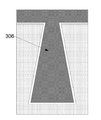
도 3e 내지 도 3g는 작은 피처 내에서 시간에 따른 갭 충진 프로세스의 개략적인 예시를 도시한다. 도 3e에서, 남아 있는 개구부가 충분히 작다고 동작 210에서 결정되고, 동작들 206 및 208이 반복되지 않는다. 벌크 코발트 충진재는 동작 212 마다 후속하여 증착된다. 도시된 바와 같이, 도 3e에서, 상단 표면들 (306b) 이 처리되었기 때문에, 이들 표면들은, 코발트가 기판 상에 증착될 때, 이들 표면들이 처리되지 않은 하단 표면들과 비교하여 보다 긴 핵생성 지연을 갖도록, 패시베이션된다. 처리된 표면에 대한 핵생성 지연은 약 200 초보다 클 수도 있다. 처리되지 않은 표면에 대한 핵생성 시간 대 처리된 표면에 대한 핵생성 시간은 처리 노출 시간에 따른다. 핵생성 시간은 시간에 따라 처리된 표면 대 처리되지 않은 표면 상의 코발트의 두께를 비교함으로써 평가될 수 있다. 예를 들어, 처리된 표면들은 약 300 초 이상인 핵생성 지연을 가질 수도 있고, 처리되지 않은 표면들은 약 20 초의 처리 노출 시간 동안 처리된 표면들보다 약 17 내지 18 ㎚ 더 코발트가 증착될 수도 있다. 보이드-프리 갭 코발트 갭 충진은 처리된 코발트층과 처리되지 않은 코발트층 사이의 높은 선택적 막 성장에 의해 가능해진다. 따라서, 도 3e의 코발트의 성장은, 피처 (306a) 의 하단부에 증착된 코발트가 계속해서 성장하도록 대부분 보텀-업이다. 도 3f에서, 306b에서의 표면들은 306a의 코발트가 대부분의 피처를 충진할 때까지 핵생성된다. 도 3g에서, 코발트 충진은 피처가 보이드-프리 코발트 (306) 로 충진되도록 완료된다.Figures 3e-3g illustrate a schematic example of a gap filling process over time in a small feature. In Figure 3E, it is determined at
도 4f에서, 상기에 기술된 바와 같이 동작들 206 및 208이 반복된 후, 동작 210에서, 남아 있는 개구부가 충분히 작은지 결정된다. 동작 212는 CVD 코발트 갭 충진이 발생하도록 수행된다. 기술된 바와 같이, 일부 실시예들에서, 예를 들어, 피처 개구부가 매우 작다면, 배리어 막이 동작 204b에서 처리된 후, 코발트 씨드층의 증착 없이, 벌크 구리층이 동작 212에서 증착된다. 그럼에도 불구하고, 도 4f에 도시된 바와 같이, 벌크 코발트가 증착되기 때문에, 상단부 (406b) 에서의 표면들은 보다 높은 핵생성 지연을 갖고 따라서 성장이 거의 보이지 않는 반면, 벌크 코발트 (406) 의 성장은 코발트의 하단 표면 (406a) 에서 보인다. 도 4g에서, 코발트는 피처의 상단부 (406b) 에서 핵생성하지만, 코발트의 하단 표면 (406a) 은 이미 대부분의 피처를 충진하였다. 도 4h는 처리 및 증착 사이클들을 사용하여 큰 피처 내에 증착된 보이드-프리 코발트 (406) 의 개략적인 예시를 제공한다.In FIG. 4F, after
장치Device
본 명세서에 제공된 증착 기법들은 PECVD (plasma enhanced chemical vapor deposition) 챔버 또는 CFD (conformal film deposition) 챔버 또는 일부 실시예들에서, ALD 챔버 내에서 구현될 수도 있다. 이러한 챔버는 많은 형태들을 취할 수도 있고, 각각이 하나 이상의 기판들 또는 웨이퍼들을 하우징할 수도 있고 다양한 기판 프로세싱 동작들을 수행하도록 구성될 수도 있는, 하나 이상의 챔버들 또는 반응기들 (때때로 복수의 스테이션들을 포함) 을 포함하는 장치의 일부일 수도 있다. 하나 이상의 챔버들은 규정된 위치 또는 위치들 내에 기판을 유지할 수도 있다 (그 위치 내에서의 운동, 예를 들어, 회전, 바이브레이션, 또는 다른 교반 (agitation) 과 함께 또는 없이). 일 구현예에서, 막 증착을 겪는 기판은 프로세스 동안 챔버 내에서 하나의 스테이션으로부터 다른 스테이션으로 이송될 수도 있다. 다른 구현예들에서, 기판은, 에칭 동작들 또는 리소그래피 동작들과 같은, 상이한 동작들을 수행하도록 장치 내에서 챔버로부터 챔버로 이송될 수도 있다. 완전한 막 증착은, 단일 스테이션에서 전체적으로 또는 임의의 증착 단계 동안 총 막 두께의 어느 부분으로 발생할 수도 있다. 프로세스 동안, 기판 각각은 페데스탈, 기판 척, 및/또는 다른 기판-홀딩 장치에 의해 제자리에 홀딩될 수도 있다. 기판이 가열되는, 특정한 동작들 동안, 장치는 히팅 플레이트와 같은 히터를 포함할 수도 있다.The deposition techniques provided herein may be implemented in a plasma enhanced chemical vapor deposition (PECVD) chamber or a conformal film deposition (CFD) chamber, or in some embodiments, in an ALD chamber. Such a chamber may take many forms, and may include one or more chambers or reactors (sometimes including a plurality of stations), each of which may house one or more substrates or wafers and be configured to perform various substrate processing operations. As shown in FIG. The one or more chambers may hold the substrate within a defined position or positions (with or without movement, e.g., rotation, vibration, or other agitation within the position). In one embodiment, the substrate undergoing film deposition may be transferred from one station to another station in the chamber during the process. In other implementations, the substrate may be transferred from the chamber to the chamber in an apparatus to perform different operations, such as etching operations or lithographic operations. Complete film deposition may occur either as a whole in a single station or at any portion of the total film thickness during any deposition step. During the process, each of the substrates may be held in place by pedestal, substrate chuck, and / or other substrate-holding devices. During certain operations, during which the substrate is heated, the apparatus may include a heater, such as a heating plate.
도 5는 본 명세서에서 기술된 방법들을 구현하기 위해 배열된 다양한 반응기 컴포넌트들을 도시하는 단순한 블록도를 제공한다. 도시된 바와 같이, 반응기 (500) 는 반응기의 다른 컴포넌트들을 둘러싸고 접지된 히터 블록 (520) 과 함께 동작하는 샤워헤드 (514) 를 포함하는 용량-방전 (capacitive-discharge) 타입 시스템에 의해 생성된 플라즈마를 포함하도록 기능하는 프로세스 챔버 (524) 를 포함한다. 고 주파수 (HF) RF 생성기 (504) 및 저 주파수 (LF) RF 생성기 (502) 는 매칭 네트워크 (506) 및 샤워헤드 (514) 에 접속될 수도 있다. 매칭 네트워크 (506) 에 의해 공급된 전력 및 주파수는 프로세스 챔버 (524) 에 공급된 프로세스 가스들로부터 플라즈마를 생성하기에 충분하다. 예를 들어, 매칭 네트워크 (506) 는 100 W 내지 1000 W의 전력을 제공할 수도 있다. 일부 예들에서, 매칭 네트워크 (506) 는 제공할 수도 있다. 통상적인 프로세스에서, HFRF 성분은 일반적으로 1 ㎒ 내지 100 ㎒, 예를 들어, 13.56 ㎒일 수도 있다. LF 성분이 있는 동작들에서, LF 성분은 약 1 ㎒ 미만, 예를 들어, 100 ㎑일 수도 있다.Figure 5 provides a simplified block diagram illustrating various reactor components arranged to implement the methods described herein. As shown, the
반응기 내에서, 웨이퍼 페데스탈 (518) 은 기판 (516) 을 지지할 수도 있다. 웨이퍼 페데스탈 (518) 은 증착 반응 및/또는 플라즈마 처리 반응 동안 그리고 반응들 사이에 기판을 홀딩하고 이송하기 위한 척, 포크 또는 리프트 핀들 (미도시) 을 포함할 수도 있다. 척은 정전 척, 기계적 척, 또는 산업 및/또는 연구를 위한 사용에 이용가능한 다양한 다른 타입들의 척일 수도 있다.Within the reactor, the
다양한 프로세스 가스들이 유입부 (512) 를 통해 도입될 수도 있다. 복수의 소스 가스 라인들 (510) 이 매니폴드 (508) 에 연결된다. 가스들은 미리 혼합될 수도 있고 되지 않을 수도 있다. 적절한 밸브 및 질량 유량 제어 메커니즘들이 올바른 프로세스 가스들이 프로세스의 증착 및 플라즈마 처리 페이즈들 동안 전달되는 것을 보장하도록 채용될 수도 있다. 화학적 전구체(들)가 액체 형태로 전달되는 경우, 액체 유량 제어 메커니즘들이 채용될 수도 있다. 이어서 이러한 액체들은 기화되고 증착 챔버에 도달하기 전에 액체 형태로 공급된 화학적 전구체의 기화점 (vaporization point) 보다 높게 가열된 매니폴드 내에서의 운송 동안 프로세스 가스들과 혼합된다.Various process gases may be introduced through the
코발트 함유 전구체 또는 질소 함유 가스와 같은, 프로세스 가스들은 유출부 (522) 를 통해 챔버 (524) 를 나갈 수도 있다. 예를 들어, 1 또는 2 단계 기계적 드라이 펌프 및/또는 터보분자 펌프 (540) 와 같은, 진공 펌프가 프로세스 챔버 (524) 밖으로 프로세스 가스들을 유출하고 프로세스 챔버 (524) 내에서 쓰로틀 밸브 또는 펜들럼 밸브와 같은 폐루프-제어된 플로우 제한 디바이스를 사용하여 적합하게 낮은 압력으로 유지하기 위해 사용될 수도 있다.Process gases, such as cobalt-containing precursors or nitrogen-containing gases, may exit the
상기에 논의된 바와 같이, 본 명세서에서 논의된 증착을 위한 기법들은 멀티-스테이션 툴 또는 단일 스테이션 툴에서 구현될 수도 있다. 도 6은 이러한 툴의 일예의 개략적인 예시이다. 특정한 구현예들에서, 4-스테이션 증착 스킴을 갖는 300 ㎜ Lam VectorTM 툴 또는 6-스테이션 증착 스킴을 갖는 200 ㎜ SequelTM 툴이 사용될 수도 있다. 일부 구현예들에서, 450 ㎜ 웨이퍼들을 프로세싱하기 위한 툴들이 사용될 수도 있다. 다양한 구현예들에서, 기판들은 매 증착 및/또는 매 증착 후 플라즈마 처리 후에 인덱싱될 수도 있고, 또는 에칭 챔버들 또는 스테이션들이 또한 동일한 툴의 일부이면 에칭 단계들 후에 인덱싱될 수도 있고, 또는 다중 증착들 및 처리들이 기판을 인덱싱하기 전에 단일 스테이션에서 수행될 수도 있다.As discussed above, the techniques for deposition discussed herein may be implemented in a multi-station tool or a single station tool. Figure 6 is a schematic illustration of an example of such a tool. In certain embodiments, a 300 mm Lam Vector TM tool with a 4-station deposition scheme or a 200 mm Sequel TM tool with a 6-station deposition scheme may be used. In some implementations, tools for processing 450 mm wafers may be used. In various implementations, the substrates may be indexed after each deposition and / or after plasma deposition, or may be indexed after the etching steps if the etching chambers or stations are also part of the same tool, And processes may be performed in a single station before indexing the substrate.
일부 실시예들에서, 본 명세서에 기술된 기법들을 수행하도록 구성된 장치가 제공될 수도 있다. 적합한 장치는 개시된 실시예들에 따른 프로세스 동작들을 제어하기 위한 인스트럭션들을 갖는 시스템 제어기 (530) 뿐만 아니라 다양한 프로세스 동작들을 수행하기 위한 하드웨어를 포함할 수도 있다. 시스템 제어기 (530) 는 통상적으로 하나 이상의 메모리 디바이스들 및 예를 들어, 밸브, RF 생성기들, 기판 핸들링 시스템들, 등과 같은 다양한 프로세스 제어 장비와 통신가능하게 연결되고, 장치가 개시된 실시예들에 따른 기법 예를 들어, 도 2의 증착 단계들에서 제공된 것과 같은 기법을 수행하도록 하는 인스트럭션들을 실행하도록 구성된 하나 이상의 프로세서들을 포함할 것이다. 본 개시에 따른 프로세스 동작들을 제어하기 위한 인스트럭션들을 포함하는 머신-판독가능한 매체는 시스템 제어기 (530) 에 커플링될 수도 있다. 제어기 (530) 는 본 명세서에 개시된 바와 같은 증착 동작들과 연관된 다양한 프로세스 파라미터들의 제어를 용이하게 하기 위해 예를 들어, 질량 유량 제어기들, 밸브들, RF 생성기들, 진공 펌프들, 등의 다양한 하드웨어 디바이스들과 통신가능하게 연결될 수도 있다.In some embodiments, an apparatus configured to perform the techniques described herein may be provided. Suitable devices may include
일부 실시예들에서, 시스템 제어기 (530) 는 반응기 (500) 의 모든 액티비티들을 제어할 수도 있다. 시스템 제어기 (530) 는 대용량 저장 디바이스에 저장되고, 메모리 디바이스로 로딩되고, 프로세서 상에서 실행되는 시스템 제어 소프트웨어를 실행할 수도 있다. 시스템 제어 소프트웨어는 가스들의 혼합, 챔버 및/또는 스테이션 압력, 챔버 및/또는 스테이션 온도, 기판 온도, 목표 전력 레벨들, RF 전력 레벨들, 기판 페데스탈, 척 및/또는 서셉터 위치, 및 반응기 (500) 에 의해 수행된 특정한 프로세스의 다른 파라미터들을 제어하기 위한 인스트럭션들뿐만 아니라 가스 플로우들의 타이밍, 기판 이동, RF 생성기 활성화, 등을 제어하기 위한 인스트럭션들을 포함할 수도 있다. 예를 들어, 소프트웨어는 코발트 함유 전구체의 플로우 레이트, 환원제의 플로우 레이트, 질소 함유 가스의 플로우 레이트, 및 상기 기술된 플로우 화학물질들 각각에 대한 노출 시간들을 제어하기 위한 인스트럭션들 또는 코드를 포함할 수도 있다. 시스템 제어 소프트웨어는 임의의 적합한 방식으로 구성될 수도 있다. 예를 들어, 다양한 프로세스 툴 컴포넌트 서브루틴들 또는 제어 객체들이 다양한 프로세스 툴 프로세스들을 수행하기 위해 필요한 프로세스 툴 컴포넌트들의 동작을 제어하기 위해 작성될 수도 있다. 시스템 제어 소프트웨어는 임의의 적합한 컴퓨터 판독가능 프로그래밍 언어로 코딩될 수도 있다.In some embodiments, the
시스템 제어기 (530) 는 통상적으로 하나 이상의 메모리 디바이스들 및 장치가 본 개시에 따른 기법을 수행하도록 인스트럭션들을 실행하도록 구성된 하나 이상의 프로세서들을 포함할 수도 있다. 개시된 실시예들에 따라 프로세스 동작들을 제어하기 위한 인스트럭션들을 포함하는 머신-판독가능 매체는 시스템 제어기 (530) 에 커플링될 수도 있다.The
상기에 기술된 바와 같이, 하나 이상의 프로세스 스테이션들이 멀티-스테이션 프로세싱 툴에 포함될 수도 있다. 도 6은 하나 또는 양자가 리모트 플라즈마 소스를 포함할 수도 있는, 인바운드 로드록 (602) 및 아웃바운드 로드록 (604) 을 갖는 멀티-스테이션 프로세싱 툴 (600) 의 실시예의 개략도를 도시한다. 대기압에서, 로봇 (606) 은 포드 (608) 를 통해 로딩된 카세트로부터 대기 포트 (610) 를 통해 인바운드 로드록 (602) 내로 기판들을 이동시키도록 구성된다. 기판은 로봇 (606) 에 의해 인바운드 로드록 (602) 내의 페데스탈 (612) 상에 위치되고, 대기 포트 (610) 는 닫히고, 로드록은 펌프다운된다. 인바운드 로드록 (602) 이 리모트 플라즈마 소스를 포함하면, 기판은 프로세싱 챔버 (614) 내에 도입되기 전에 로드록 내의 리모트 플라즈마 처리에 노출될 수도 있다. 게다가, 기판은 또한 예를 들어, 수분 및 흡수된 가스들을 제거하기 위해, 인바운드 로드록 (602) 내에서 가열될 수도 있다. 다음에, 챔버 이동 포트 (616) 가 프로세싱 챔버 (614) 에 대해 개방되고, 또 다른 로봇 (미도시) 이 프로세싱을 위한 반응기 내에 도시된 제 1 스테이션의 페데스탈 상의 반응기 내에 웨이퍼를 위치시킨다. 도 6에 도시된 실시예는 로드록들을 포함하지만, 일부 실시예들에서, 프로세스 스테이션에 기판이 직접적으로 제공될 수도 있다는 것이 이해될 것이다.As described above, one or more process stations may be included in the multi-station processing tool. Figure 6 shows a schematic diagram of an embodiment of a
도시된 프로세싱 챔버 (614) 는 도 6에 도시된 실시예에서 1 내지 4로 번호가 붙여진, 4 개의 프로세스 스테이션들을 포함한다. 스테이션 각각은 가열된 페데스탈 (스테이션 1에 대해 618로 도시됨), 및 가스 라인 유입부들을 갖는다. 일부 스테이션들은 도 5에 대하여 상기 기술된 컴포넌트들과 유사한 컴포넌트들을 포함할 수도 있다. 일부 실시예들에서, 프로세스 스테이션 각각이 상이한 목적 또는 다수의 목적들을 가질 수도 있다는 것이 이해될 것이다. 예를 들어, 일부 실시예들에서, 프로세스 스테이션은 ALD 프로세스 모드와 CVD 프로세스 모드 사이에서 전환가능할 수도 있다. 부가적으로 또는 대안적으로, 일부 실시예들에서, 프로세싱 챔버 (614) 는 ALD 프로세스 스테이션과 CVD 프로세스 스테이션의 하나 이상의 매칭된 쌍들을 포함할 수도 있다. 일부 실시예들에서, 피처들은 ALD 또는 CVD 를 사용하여 일 스테이션 (예를 들어, 스테이션 1) 에서 열적으로 (예를 들어, 플라즈마를 사용하지 않고) 코발트로 부분적으로 충진될 수도 있다. 이어서, 기판은 기판이 질소 함유 가스 및 플라즈마에 노출되고, 이어서 CVD에 의해 벌크 코발트를 증착하기 위해 코발트 함유 전구체 및 환원제에 노출되는, 동일한 챔버 (614) 내의 제 2 스테이션 (예를 들어, 스테이션 2) 으로, 또는 상이한 챔버의 스테이션으로 이송될 수도 있다. 일부 실시예들에서, 환원제는 질소 함유 가스가 챔버 내로 흐르는 동안 플라즈마 노출과 교번한다. 질소 함유 가스 및/또는 환원제는 문제의 기판이 있는 스테이션 (예를 들어, 스테이션 2) 에만 도입되거나, 전체 챔버 (614) 에 도입될 수도 있다.The illustrated
다양한 실시예들에서, 기판은 제 2 스테이션으로 이송되지 않는다. 오히려, 기판은 열적 증착 동안 동일한 스테이션 (예를 들어, 스테이션 1) 에 남지만, 스테이션은 또한 열적 증착 후에 환원제, 질소 함유 가스, 및 플라즈마를 스테이션으로 도입하도록 구비된다.In various embodiments, the substrate is not transported to the second station. Rather, the substrate remains in the same station (e.g., station 1) during thermal deposition, but the station is also adapted to introduce the reducing agent, nitrogen containing gas, and plasma into the station after thermal deposition.
일부 실시예들에서, 기판이 코발트의 열적 증착을 겪은 후, 기판은, 또한 다양한 스테이션들을 포함할 수도 있는 상이한 챔버로 이송된다. 도시된 프로세싱 챔버 (614) 는 4 개의 스테이션들을 포함하지만, 본 개시에 따른 프로세싱 챔버는 임의의 적합한 수의 스테이션들을 가질 수도 있다는 것이 이해될 것이다. 예를 들어, 일부 실시예들에서, 프로세싱 챔버는 5 개 이상의 스테이션들을 가질 수도 있지만, 다른 실시예들에서 프로세싱 챔버는 3 개 이하의 스테이션들을 가질 수도 있다.In some embodiments, after the substrate undergoes thermal deposition of cobalt, the substrate is transferred to a different chamber, which may also include various stations. It will be appreciated that although the illustrated
도 6은 프로세싱 챔버 (614) 내에서 웨이퍼들의 이송을 위한 웨이퍼 핸들링 시스템 (609) 의 일 실시예를 도시한다. 일부 실시예들에서, 웨이퍼 핸들링 시스템 (609) 은 다양한 프로세스 스테이션들 사이 및/또는 프로세스 스테이션과 로드록 사이에서 웨이퍼들을 이송할 수도 있다. 임의의 적합한 웨이퍼 핸들링 시스템이 채용될 수도 있다는 것이 이해될 것이다. 비제한적인 예들은 웨이퍼 캐로절들 및 웨이퍼 핸들링 로봇들을 포함한다. 도 6은 또한 프로세스 툴 (600) 의 프로세스 조건들 및 하드웨어 상태들을 제어하도록 채용된 시스템 제어기 (650) 의 일 실시예를 도시한다. 시스템 제어기 (650) 는 하나 이상의 메모리 디바이스들 (656), 하나 이상의 대용량 저장 디바이스들 (654), 및 하나 이상의 프로세서들 (652) 을 포함할 수도 있다. 프로세서 (652) 는 CPU 또는 컴퓨터, 아날로그 입력/출력 접속부 및/또는 디지털 입력/출력 접속부, 스텝퍼 모터 제어기 보드들, 등을 가질 수도 있다.6 illustrates one embodiment of a
일부 실시예들에서, 시스템 제어기 (650) 는 프로세스 툴 (600) 의 모든 액티비티들을 제어한다. 시스템 제어기 (650) 는 대용량 저장 디바이스 (654) 에 저장되고, 메모리 디바이스 (656) 로 로딩되고, 프로세서 (652) 상에서 실행되는 시스템 제어 소프트웨어 (658) 를 실행한다. 대안적으로, 제어 로직은 시스템 제어기 (650) 내에서 하드코딩될 수도 있다. ASIC (Applications Specific Integrated Circuits), PLD (Programmable Logic Devices) (예를 들어, FPGA, field-programmable gate arrays) 등이 이들 목적들을 위해 사용될 수도 있다. 이하의 논의에서, "소프트웨어" 또는 "코드"가 사용되면, 대신 기능적으로 비교가능한 하드코딩된 로직이 사용될 수도 있다. 시스템 제어 소프트웨어 (658) 는 타이밍, 가스들의 혼합, 챔버 및/또는 스테이션 압력, 챔버 및/또는 스테이션 온도, 웨이퍼 온도, 목표 전력 레벨들, RF 전력 레벨들, 기판 페데스탈, 척 및/또는 서셉터 위치, 및 프로세스 툴 (600) 에서 수행된 특정한 프로세스의 다른 파라미터들을 제어하기 위한 인스트럭션들을 포함할 수도 있다. 시스템 제어 소프트웨어 (658) 는 임의의 적합한 방식으로 구성될 수도 있다. 예를 들어, 다양한 프로세스 툴 컴포넌트 서브루틴들 또는 제어 객체들이 다양한 프로세스 툴 프로세스들을 수행하기 위해 필요한 프로세스 툴 컴포넌트들의 동작을 제어하도록 작성될 수도 있다. 시스템 제어 소프트웨어 (658) 는 임의의 적합한 컴퓨터 판독가능 프로그래밍 언어로 코딩될 수도 있다.In some embodiments, the
일부 실시예들에서, 시스템 제어 소프트웨어 (658) 는 상기 기술된 다양한 파라미터들을 제어하기 위한 IOC (input/output control) 시퀀싱 (sequencing) 인스트럭션들을 포함할 수도 있다. 시스템 제어기 (650) 와 연관된 대용량 저장 디바이스 (654) 및/또는 메모리 디바이스 (656) 에 저장된 다른 컴퓨터 소프트웨어 및/또는 프로그램들이 일부 실시예들에서 채용될 수도 있다. 이러한 목적을 위한 프로그램들 또는 프로그램들의 섹션들의 예들은 기판 포지셔닝 (positioning) 프로그램, 프로세스 가스 제어 프로그램, 압력 제어 프로그램, 히터 제어 프로그램, 및 플라즈마 제어 프로그램을 포함한다.In some embodiments, the
기판 포지셔닝 프로그램은 페데스탈 (618) 상에 기판을 로딩하고 기판과 프로세스 툴 (600) 의 다른 부분들 사이의 공간을 제어하도록 사용된 프로세스 툴 컴포넌트들에 대한 프로그램 코드를 포함할 수도 있다.The substrate positioning program may include program code for process tool components used to load the substrate on the
프로세스 가스 제어 프로그램은 프로세스 스테이션 내의 압력을 안정화시키기 위해 증착 전에 가스 조성 (예를 들어, 본 명세서에 기술된 바와 같이 코발트 함유 전구체, 환원제, 및 질소 함유 가스) 및 플로우 레이트들을 제어하기 위한 코드 및 선택적으로 하나 이상의 프로세스 스테이션들로 가스를 흘리기 위한 코드를 포함할 수도 있다. 압력 제어 프로그램은 예를 들어, 프로세스 스테이션의 배기 시스템의 쓰로틀 밸브, 프로세스 스테이션으로의 가스 플로우, 등을 조절함으로써 프로세스 스테이션 내의 압력을 제어하기 위한 코드를 포함할 수도 있다.The process gas control program includes a code for controlling the gas composition (e.g., the cobalt-containing precursor, the reducing agent, and the nitrogen-containing gas as described herein) and the flow rates before deposition to stabilize the pressure in the process station, As well as code for flowing gas to one or more process stations. The pressure control program may include a code for controlling the pressure in the process station by, for example, adjusting the throttle valve of the exhaust system of the process station, the gas flow to the process station, and the like.
일부 구현예들에서, 시스템 제어기 (650) 는 상술한 예들의 일부일 수도 있는 시스템의 일부이다. 이러한 시스템들은, 프로세싱 툴 또는 툴들, 챔버 (614) 와 같은 챔버 또는 챔버들, 프로세싱을 위한 플랫폼 또는 플랫폼들, 및/또는 특정 프로세싱 컴포넌트들 (웨이퍼 페데스탈, 가스 플로우 시스템, 등) 을 포함하는, 반도체 프로세싱 장비를 포함할 수 있다. 이러한 시스템들은 반도체 웨이퍼 또는 기판의 프로세싱 이전에, 프로세싱 동안에 그리고 프로세싱 이후에 그들의 동작을 제어하기 위한 전자장치에 통합될 수 있다. 전자장치는 시스템 또는 시스템들의 다양한 컴포넌트들 또는 하위부품들을 제어할 수 있는 "제어기"로서 지칭될 수도 있다. 시스템 제어기 (650) 는, 시스템의 프로세싱 요건들 및/또는 타입에 따라서, 프로세싱 가스들의 전달, 온도 설정사항들 (예를 들어, 가열 및/또는 냉각), 압력 설정사항들, 진공 설정사항들, 전력 설정사항들, 무선 주파수 (RF) 생성기 설정사항들, RF 매칭 회로 설정사항들, 주파수 설정사항들, 플로우 레이트 설정사항들, 유체 전달 설정사항들, 위치 및 동작 설정사항들, 툴들 및 다른 이송 툴들 및/또는 특정 시스템과 연결되거나 인터페이싱된 로드록들 내외로의 웨이퍼 이송들을 포함하는, 본 명세서에 개시된 프로세스들 중 임의의 프로세스들을 제어하도록 프로그램될 수도 있다.In some implementations, the
일반적으로 말하면, 시스템 제어기 (650) 는 인스트럭션들을 수신하고, 인스트럭션들을 발행하고, 동작을 제어하고, 세정 동작들을 인에이블하고, 엔드포인트 측정들을 인에이블하는 등을 하는 다양한 집적 회로들, 로직, 메모리, 및/또는 소프트웨어를 갖는 전자장치로서 규정될 수도 있다. 집적 회로들은 프로그램 인스트럭션들을 저장하는 펌웨어의 형태의 칩들, 디지털 신호 프로세서들 (DSP), ASIC (application specific integrated circuit) 으로서 규정되는 칩들 및/또는 프로그램 인스트럭션들 (예를 들어, 소프트웨어) 을 실행하는 하나 이상의 마이크로프로세서들, 또는 마이크로제어기들을 포함할 수도 있다. 프로그램 인스트럭션들은 반도체 웨이퍼 상에서 또는 반도체 웨이퍼에 대한 특정 프로세스를 실행하기 위한 동작 파라미터들을 규정하는, 다양한 개별 설정사항들 (또는 프로그램 파일들) 의 형태로 시스템 제어기 (650) 로 또는 시스템으로 전달되는 인스트럭션들일 수 있다. 일부 실시예들에서, 동작 파라미터들은 하나 이상의 층들, 재료들, 금속들, 산화물들, 실리콘, 이산화 실리콘, 표면들, 회로들, 및/또는 웨이퍼의 다이들의 제조 동안에 하나 이상의 프로세싱 단계들을 달성하도록 프로세스 엔지니어에 의해서 규정된 레시피의 일부일 수도 있다. 예를 들어, 파라미터들은 코발트 함유 전구체 가스 플로우, 환원제 가스 플로우, 캐리어 가스 플로우, 질소 함유 가스 플로우, 플라즈마 전력 및 주파수, 페데스탈 온도, 스테이션 또는 챔버 압력 및/또는 온도, 및 다른 것들을 포함할 수도 있다.Generally speaking, the
시스템 제어기 (650) 는, 일부 구현예들에서, 시스템에 통합되거나, 시스템에 커플링되거나, 이와 달리 시스템에 네트워킹되거나, 또는 이들의 조합으로 될 수 있는 컴퓨터에 커플링되거나 이의 일부일 수 있다. 예를 들어, 시스템 제어기 (650) 는 웨이퍼 프로세싱의 원격 액세스를 가능하게 할 수 있는 공장 (fab) 호스트 컴퓨터 시스템의 전부 또는 일부이거나 "클라우드" 내에 있을 수도 있다. 컴퓨터는 제조 동작들의 현 진행을 모니터링하고, 과거 제조 동작들의 이력을 조사하고, 복수의 제조 동작들로부터 경향들 또는 성능 계측치들을 조사하고, 현 프로세싱의 파라미터들을 변경하고, 현 프로세싱을 따르는 프로세싱 단계들을 설정하고, 또는 새로운 프로세스를 시작하기 위해서 시스템으로의 원격 액세스를 인에이블할 수도 있다. 일부 예들에서, 원격 컴퓨터 (예를 들어, 서버) 는 로컬 네트워크 또는 인터넷을 포함할 수도 있는 네트워크를 통해서 프로세스 레시피들을 시스템에 제공할 수 있다. 원격 컴퓨터는 차후에 원격 컴퓨터로부터 시스템으로 전달될 파라미터들 및/또는 설정사항들의 입력 또는 프로그래밍을 가능하게 하는 사용자 인터페이스를 포함할 수 있다. 일부 예들에서, 시스템 제어기 (650) 는 하나 이상의 동작들 동안에 수행될 프로세스 단계들 각각에 대한 파라미터들을 특정한, 데이터의 형태의 인스트럭션들을 수신한다. 이 파라미터들은 시스템 제어기 (650) 가 제어하거나 인터페이싱하도록 구성된 툴의 타입 및 수행될 프로세스의 타입에 특정적일 수 있다는 것이 이해되어야 한다. 따라서, 상술한 바와 같이, 시스템 제어기 (650) 는 예를 들어 서로 네트워킹되어서 함께 공통 목적, 예를 들어 본 명세서에 기술된 프로세스들 및 제어들을 위해서 협력하는 하나 이상의 개별 제어기들을 포함함으로써 분산될 수도 있다. 이러한 목적을 위한 분산형 제어기 (650) 의 예는 챔버 상의 프로세스를 제어하도록 조합되는, (예를 들어, 플랫폼 레벨에서 또는 원격 컴퓨터의 일부로서) 원격으로 위치한 하나 이상의 집적 회로들과 통신하는 챔버 상의 하나 이상의 집적 회로들일 수 있다.The
비제한적으로, 예시적인 시스템들은 플라즈마 에칭 챔버 또는 모듈, 증착 챔버 또는 모듈, 스핀-린스 챔버 또는 모듈, 금속 도금 챔버 또는 모듈, 세정 챔버 또는 모듈, 베벨 에지 에칭 챔버 또는 모듈, PVD (physical vapor deposition) 챔버 또는 모듈, CVD (chemical vapor deposition) 챔버 또는 모듈, ALD (atomic layer deposition) 챔버 또는 모듈, ALE (atomic layer etch) 챔버 또는 모듈, 이온 주입 챔버 또는 모듈, 트랙 (track) 챔버 또는 모듈, 및 반도체 웨이퍼들의 제조 및/또는 가공 시에 사용되거나 연관될 수도 있는 임의의 다른 반도체 프로세싱 시스템들을 포함할 수도 있다.Exemplary systems include, but are not limited to, a plasma etch chamber or module, a deposition chamber or module, a spin-rinse chamber or module, a metal plating chamber or module, a cleaning chamber or module, a bevel edge etch chamber or module, A chamber or module, a chemical vapor deposition (CVD) chamber or module, an ALD (atomic layer deposition) chamber or module, an ALE (atomic layer etch) chamber or module, an ion implantation chamber or module, a track chamber or module, And may include any other semiconductor processing systems that may be used or associated with during fabrication and / or processing of wafers.
상술한 바와 같이, 툴에 의해서 수행될 프로세스 단계 또는 단계들에 따라서, 시스템 제어기 (650) 는, 반도체 제작 공장 내의 툴 위치들 및/또는 로드 포트들로부터/로 웨이퍼들의 컨테이너들을 이동시키는 재료 이송 시에 사용되는, 다른 툴 회로들 또는 모듈들, 다른 툴 컴포넌트들, 툴 (600) 과 같은 클러스터 툴들, 다른 툴 인터페이스들, 인접 툴들, 이웃하는 툴들, 공장 도처에 위치한 툴들, 메인 컴퓨터, 다른 제어기 (650) 또는 툴들 중 하나 이상과 통신할 수도 있다.As described above, depending on the process steps or steps to be performed by the tool, the
히터 제어 프로그램은 기판을 히팅하기 위해 사용된 히팅 유닛으로의 전류를 제어하기 위한 코드를 포함할 수도 있다. 대안적으로, 히터 제어 프로그램은 기판으로의 (헬륨과 같은) 열 전달 가스 (heat transfer gas) 의 전달을 제어할 수도 있다.The heater control program may include code for controlling the current to the heating unit used to heat the substrate. Alternatively, the heater control program may control the transfer of heat transfer gas (such as helium) to the substrate.
플라즈마 제어 프로그램은 본 명세서의 실시예들에 따라 하나 이상의 프로세스 스테이션들 내의 프로세스 전극들에 인가된 RF 전력 레벨들을 설정하기 위한 코드를 포함할 수도 있다.The plasma control program may comprise code for setting the RF power levels applied to the process electrodes in one or more process stations in accordance with the embodiments herein.
압력 제어 프로그램은 본 명세서의 실시예들에 따라 반응 챔버 내의 압력을 유지하기 위한 코드를 포함할 수도 있다.The pressure control program may comprise a code for maintaining the pressure in the reaction chamber in accordance with the embodiments herein.
일부 실시예들에서, 시스템 제어기 (650) 와 연관된 사용자 인터페이스가 있을 수도 있다. 사용자 인터페이스는 디스플레이 스크린, 장치의 그래픽적인 소프트웨어 디스플레이 및/또는 프로세스 조건들의 그래픽적인 소프트웨어 디스플레이, 및 포인팅 디바이스들, 키보드들, 터치 스크린들, 마이크로폰들 등과 같은 사용자 입력 디바이스들을 포함할 수도 있다.In some embodiments, there may be a user interface associated with the
일부 실시예들에서, 시스템 제어기 (650) 에 의해 조정된 파라미터들은 프로세스 조건들과 관련될 수도 있다. 비제한적인 예들은 프로세스 가스 조성 및 플로우 레이트들, 온도, 압력, (RF 바이어스 전력 레벨들과 같은) 플라즈마 조건들, 등을 포함한다. 이들 파라미터들은 사용자 인터페이스를 활용하여 입력될 수도 있는, 레시피의 형태로 사용자에게 제공될 수도 있다.In some embodiments, the parameters adjusted by the
프로세스를 모니터링하기 위한 신호들은 다양한 프로세스 툴 센서들로부터 시스템 제어기 (650) 의 아날로그 입력 접속부 및/또는 디지털 입력 접속부에 의해 제공될 수도 있다. 프로세스를 제어하기 위한 신호들은 프로세스 툴 (600) 의 아날로그 출력 접속부 및/또는 디지털 출력 접속부 상에 출력될 수도 있다. 모니터링될 수도 있는 프로세스 툴 센서들의 비제한적인 예들은 질량 유량 제어기들, (압력계들 (manometers) 과 같은) 압력 센서들, 열전대들 (thermocouple), 등을 포함한다. 적절하게 프로그램된 피드백 및 제어 알고리즘들이 프로세스 조건들을 유지하기 위해 이들 센서들로부터의 데이터와 함께 사용될 수도 있다.Signals for monitoring the process may be provided by the analog input and / or digital input connections of the
시스템 제어기 (650) 는 상기 기술된 증착 프로세스들을 구현하기 위한 프로그램 인스트럭션들을 제공할 수도 있다. 프로그램 인스트럭션들은 DC 전력 레벨, RF 전력 레벨, RF 바이어스 전력 레벨, 압력, 온도, 등과 같은 다양한 프로세스 파라미터들을 제어할 수도 있다. 인스트럭션들은 본 명세서에 기술된 다양한 실시예들에 따른 막 스택들의 인 시추 증착을 동작시키기 위한 파라미터들을 제어할 수도 있다.The
시스템 제어기는 통상적으로 하나 이상의 메모리 디바이스들 및 장치가 본 실시예들에 따른 방법을 수행하도록 인스트럭션들을 실행하도록 구성된 하나 이상의 프로세서들을 포함할 것이다. 본 실시예들에 따른 프로세스 동작들을 제어하기 위한 인스트럭션들을 포함하는 머신-판독가능 매체는 시스템 제어기와 커플링될 수도 있다.The system controller will typically include one or more memory devices and one or more processors configured to execute instructions to perform the method according to the embodiments. A machine-readable medium including instructions for controlling process operations in accordance with the present embodiments may be coupled with a system controller.
본 명세서에 개시된 방법들을 수행하기 위한 적절한 장치는, 각각 전체가 본 명세서에 인용된, 명칭이 "PLASMA ACTIVATED CONFORMAL FILM DEPOSITION"이고 2011년 4월 11일 출원된 미국 특허 출원 번호 제 13/084,399 호 (이제 미국 특허 등록 번호 제 8,728,956 호) 및 명칭이 "SILICON NITRIDE FILMS AND METHODS"이고 2011년 4월 11일 출원된 미국 특허 출원 번호 제 13/084,305 호에서 더 논의되고 기술되었다.Appropriate devices for carrying out the methods disclosed herein are described in U.S. Patent Application No. 13 / 084,399, entitled " PLASMA ACTIVATED CONFORMAL FILM DEPOSITION ", each of which is incorporated herein by reference in its entirety and which was filed on April 11, U.S. Patent No. 8,728,956), and U.S. Patent Application Serial No. 13 / 084,305, filed April 11, 2011, entitled "SILICON NITRIDE FILMS AND METHODS".
본 명세서에 기술된 장치/프로세스는 예를 들어 반도체 디바이스들, 디스플레이들, LED들, 광전 패널들 등의 제조 또는 제작을 위한 리소그래피 패터닝 툴들 또는 프로세스들과 함께 사용될 수도 있다. 통상적으로, 이러한 툴들/프로세스들은 반드시 그러한 것은 아니지만 공통 제조 시설 내에서 함께 사용 또는 수행될 수 있다. 막의 리소그래피 패터닝은 통상적으로 각각 다수의 가능한 툴을 사용하여서 실현되는 다음의 단계들 중 몇몇 또는 모두를 포함하며, 이 단계들은 (1) 스핀 온 또는 스프레이 온 툴을 사용하여 워크피스, 즉 기판 상에 포토레지스트를 도포하는 단계, (2) 고온 플레이트 또는 노 또는 UV 경화 툴을 사용하여 포토레지스트를 경화하는 단계, (3) 웨이퍼 스텝퍼와 같은 툴을 사용하여 포토레지스트를 가시광선 또는 자외선 또는 x 선 광에 노출시키는 단계, (4) 습식 벤치 (wet bench) 와 같은 툴을 사용하여 레지스트를 선택적으로 제거하여 이를 패터닝하도록 포토레지스트를 현상하는 단계, (5) 건식 또는 플라즈마-보조 에칭 툴을 사용하여 아래에 놓인 막 또는 워크피스에 레지스트 패턴을 전사하는 단계, (6) RF 또는 마이크로파 플라즈마 레지스트 스트립퍼 (stripper) 와 같은 툴을 사용하여 포토레지스트를 제거하는 단계를 포함할 수 있다.The device / process described herein may be used in conjunction with lithographic patterning tools or processes for the fabrication or fabrication of, for example, semiconductor devices, displays, LEDs, photoelectric panels, and the like. Typically, these tools / processes are not necessarily, but can be used or performed together in a common manufacturing facility. Lithographic patterning of the film typically includes some or all of the following steps, each of which is accomplished using a number of possible tools, which may include (1) applying a spin on or spray on tool to the workpiece, (2) curing the photoresist using a hot plate or furnace or UV curing tool, (3) exposing the photoresist to visible or ultraviolet or x-ray light using a tool such as a wafer stepper, (4) selectively removing the resist using a tool such as a wet bench and developing the photoresist to pattern it, (5) applying a dry or plasma-assisted etching tool Transferring the resist pattern to a film or a workpiece placed on the substrate, (6) RF or microwave plasma resist stripper, And removing the photoresist using a tool such as a photoresist.
실험Experiment
실험 1
처리된 코발트 막 및 처리되지 않은 코발트 막에 대한 핵생성 지연들을 비교하기 위한 실험이 수행되었다. 블랭킷 코발트 씨드층들이 2 개의 기판들 상에 증착된다. 일 기판 상에서, 표면들은 20 초 동안 80 ℃의 온도로 질소 및 플라즈마에 처리된다. 다른 기판은 처리되지 않는다. 이어서 두 기판들은 코발트 CVD 벌크 증착 시 코발트 함유 전구체 및 수소에 노출된다. 코발트 씨드층 상에 형성된 코발트의 양은 시간에 따라 측정되었다.Experiments were performed to compare nucleation delays for the treated cobalt film and the untreated cobalt film. The blanket cobalt seed layers are deposited on two substrates. On one substrate, the surfaces are treated with nitrogen and plasma at a temperature of 80 DEG C for 20 seconds. Other substrates are not processed. Both substrates are then exposed to cobalt-containing precursors and hydrogen upon cobalt CVD bulk deposition. The amount of cobalt formed on the cobalt seed layer was measured over time.
도 7은 증착 시 코발트의 다양한 두께를 시간에 따라 도시하는 플롯이다. 삼각형 플롯들 (702) 은 처리되지 않은 코발트 씨드층에 대해 측정된 두께들을 나타낸다. 삼각형 플롯들은 핵생성 지연이 거의 없거나 전혀 없다는 것을 나타낸다. 원형 플롯들 (704) 은 처리된 코발트층에 대해 측정된 두께들을 나타낸다. 핵생성 지연은 약 200 초를 넘는다. 코발트 핵생성 후 처리된 기판들과 처리되지 않은 기판들 모두에 대한 증착 레이트는 비슷하다 (처리되지 않은 코발트에 대해 0.065 ㎚/s, 처리된 코발트에 대해 0.066 ㎚/s). 이들 결과들은 질소 및 플라즈마로의 코발트 막의 노출이, 피처의 상단에서 또는 상단 근방에서 보이드들을 감소시키기 위해 핵생성을 지연시킴으로써 피처들이 코발트로 충진될 수도 있도록 핵생성 지연을 증가시킬 수도 있다는 것을 암시한다.Figure 7 is a plot showing the various thicknesses of cobalt in time during deposition. Triangle plots 702 represent measured thicknesses for the untreated cobalt seed layer. Triangle plots indicate little or no nucleation delay. Circular plots 704 represent measured thicknesses for the treated cobalt layer. The nucleation delay is over about 200 seconds. The deposition rates for both treated and untreated substrates after cobalt nucleation are similar (0.065 nm / s for untreated cobalt and 0.066 nm / s for treated cobalt). These results imply that exposure of the cobalt film to nitrogen and plasma may increase the nucleation delay so that the features may be filled with cobalt by delaying nucleation to reduce voids at or near the top of the feature .
실험 2
코발트 막들 상에서 노출 시간들을 비교하기 위한 실험이 수행되었다. 3 회의 시도들이, 각각 도 2의 동작 202에서 상기 기술된 방법들에 따라 증착된 코발트 막의 블랭킷층 상에서 수행되었다. 코발트는 각각 80 ℃에서 질소 및 플라즈마에 5 초, 20 초, 및 60 초 동안 노출되었다. 기판들은 후속하여, CVD에 의해 벌크 코발트층을 증착하기 위해 코발트 함유 전구체 및 수소에 노출되었다. 처리된 표면들 상에 새롭게 증착된 코발트의 두께가 측정되고 결과들이 도 8에 플롯팅되었다. 5 초 처리 후에 증착된 코발트의 두께는 삼각형 플롯들로 도시되고, 20 초 처리는 사각형 플롯들로 도시되고, 60 초 처리는 원형 플롯들로 도시된다.Experiments were performed to compare exposure times on cobalt films. Three trials were performed on the blanket layer of the cobalt film deposited according to the methods described above in
도시된 바와 같이, 처리된 막들은 약 5 초에 포화되고, 이는 코발트 막 핵생성을 단시간 지체시키기 위해 사용될 수도 있는 처리된 표면 (예를 들어, 코발트 나이트라이드 표면) 을 효과적으로 생성한다는 것을 나타낸다.As shown, the treated films saturate in about 5 seconds, indicating that they effectively produce a treated surface (e.g., a cobalt nitride surface) that may be used to retard cobalt film nucleation for a short period of time.
실험 3
본 명세서에 기술된 방법들을 사용하여 코발트가 증착된 피처들을 비교하기 위한 실험이 수행되었다. 기판 각각은 재차 들어간 피처들을 갖는 피처들을 포함한다. 일 기판은 도 2에 대하여 상기 기술된 방법을 사용하여 증착되었다. 제 2 기판은 처리되지 않은 코발트를 사용하여 증착되었다 - 코발트 씨드층이 먼저 증착되고, 이어서 코발트의 CVD 벌크 충진. 증착된 막들의 SEM 화상들이 도 9a 및 도 9b에 도시된다. 도 9a는 처리 없이 증착된 피처들을 도시한다. 피처들 (900) 은 증착된 코발트 (906) 를 포함하지만, 보이드 (960) 가 두 피처들 내에 형성되었다는 것을 주의한다. 도 9b는 처리를 사용하여 증착된 피처들을 도시한다. 피처들 (980) 은 보이드들 없이 코발트 (986) 로 충진되었다.Experiments were conducted to compare features deposited with cobalt using the methods described herein. Each of the substrates includes features having reentered features. One substrate was deposited using the method described above with respect to FIG. The second substrate was deposited using untreated cobalt - the cobalt seed layer was deposited first, followed by CVD bulk filling of cobalt. SEM images of the deposited films are shown in Figures 9A and 9B. Figure 9a shows the features deposited without processing. Note that features 900 include deposited
결론conclusion
전술한 실시예들이 이해의 명확성을 목적으로 다소 상세히 기술되었지만, 특정한 변화들 및 수정들이 첨부된 청구항들의 범위 내에서 실시될 수 있다는 것이 이해될 것이다. 본 실시예들의 프로세스들, 시스템들, 및 장치를 구현하는 많은 대안적인 방식들이 있다는 것을 주목해야 한다. 따라서, 본 실시예들은 예시적이고 비제한적인 것으로 간주되고, 실시예들은 본 명세서에 주어진 상세들로 제한되는 것은 아니다.While the foregoing embodiments have been described in some detail for purposes of clarity of understanding, it will be understood that certain changes and modifications may be practiced within the scope of the appended claims. It should be noted that there are many alternative ways of implementing the processes, systems, and devices of the present embodiments. Accordingly, the embodiments are to be considered as illustrative and not restrictive, and the embodiments are not limited to the details given herein.
Claims (20)
(a) 하나 이상의 피처들을 갖는 기판을 제공하는 단계로서, 상기 피처들 각각은 피처 개구부를 포함하는, 상기 기판을 제공하는 단계;
(b) 피처 각각 내에 차동 억제 프로파일이 있도록, 상기 피처 개구부들에서 또는 상기 피처 개구부들 근방의 상기 하나 이상의 피처들의 표면들 상에서 코발트 핵생성을 선택적으로 억제하는 단계; 및
(c) 상기 차동 억제 프로파일에 따라 상기 피처 내에 코발트를 증착하는 단계를 포함하는, 반도체 기판을 프로세싱하는 방법.CLAIMS 1. A method of processing a semiconductor substrate,
(a) providing a substrate having one or more features, each of the features comprising a feature opening;
(b) selectively inhibiting cobalt nucleation on the surfaces of the one or more features at or near the feature openings such that there is a differential suppression profile within each feature; And
(c) depositing cobalt within the feature in accordance with the differential suppression profile.
상기 코발트 핵생성을 선택적으로 억제하는 단계 전에, 상기 피처들 상에 배리어층을 증착하는 단계를 더 포함하는, 반도체 기판을 프로세싱하는 방법.The method according to claim 1,
Further comprising depositing a barrier layer on the features prior to selectively inhibiting the cobalt nucleation. ≪ RTI ID = 0.0 > 11. < / RTI >
상기 배리어층은 티타늄, 티타늄 나이트라이드, 텅스텐, 텅스텐 나이트라이드, 탄탈룸, 탄탈룸 나이트라이드, 루테늄, 및 코발트 나이트라이드로 구성된 그룹으로부터 선택되는, 반도체 기판을 프로세싱하는 방법.3. The method of claim 2,
Wherein the barrier layer is selected from the group consisting of titanium, titanium nitride, tungsten, tungsten nitride, tantalum, tantalum nitride, ruthenium, and cobalt nitride.
상기 코발트 핵생성을 선택적으로 억제하는 단계 전에, 상기 하나 이상의 피처들을 부분적으로 충진하기 위해, 상기 기판을 코발트 함유 전구체에 노출시키는 단계를 더 포함하는, 반도체 기판을 프로세싱하는 방법.The method according to claim 1,
Further comprising exposing the substrate to a cobalt-containing precursor to partially fill the at least one feature prior to selectively inhibiting the cobalt nucleation. ≪ Desc / Clms Page number 19 >
상기 방법은 약 400 ℃ 미만의 온도로 수행되는, 반도체 기판을 프로세싱하는 방법.The method according to claim 1,
Wherein the method is performed at a temperature of less than about < RTI ID = 0.0 > 400 C. < / RTI >
상기 코발트 함유 전구체는 디카르보닐 사이클로펜타디에닐 코발트 (dicarbonyl cyclopentadienyl cobalt), 코발트 카르보닐, 다양한 코발트 아미디네이트 전구체들 (cobalt amidinate precursors), 코발트 디아자디에닐 착체들 (cobalt diazadienyl complexes), 코발트 아미디네이트/구아니디네이트 전구체들 (cobalt amidinate/guanidinate precursors), 및 이들의 조합들로 구성된 그룹으로부터 선택되는, 반도체 기판을 프로세싱하는 방법.5. The method of claim 4,
The cobalt-containing precursor may be selected from the group consisting of dicarbonyl cyclopentadienyl cobalt, cobalt carbonyl, various cobalt amidinate precursors, cobalt diazadienyl complexes, Amidinate / guanidinate precursors, and combinations thereof. ≪ Desc / Clms Page number 12 >
상기 피처 개구부들에서 또는 상기 피처 개구부들 근방의 상기 피처들의 상기 표면들은 상기 피처 측벽들의 상단 약 10 % 내지 약 50 %를 포함하는, 반도체 기판을 프로세싱하는 방법.7. The method according to any one of claims 1 to 6,
Wherein the surfaces of the features at or near the feature openings comprise about 10% to about 50% of the top of the feature sidewalls.
상기 코발트 핵생성을 선택적으로 억제하는 단계는, 질소 함유 가스로부터 생성된 플라즈마에 상기 기판을 노출시키는 단계를 더 포함하는, 반도체 기판을 프로세싱하는 방법.7. The method according to any one of claims 1 to 6,
Wherein selectively inhibiting the cobalt nucleation further comprises exposing the substrate to a plasma generated from a nitrogen containing gas.
상기 기판은 약 300 초 미만의 시간 동안 상기 질소 함유 가스로부터 생성된 상기 플라즈마에 노출되는, 반도체 기판을 프로세싱하는 방법.9. The method of claim 8,
Wherein the substrate is exposed to the plasma generated from the nitrogen containing gas for less than about 300 seconds.
상기 플라즈마는 지향성인 (directional), 반도체 기판을 프로세싱하는 방법.9. The method of claim 8,
Wherein the plasma is directional.
상기 피처들은 재차 들어간 (re-entrant) 프로파일들을 포함하는, 반도체 기판을 프로세싱하는 방법.7. The method according to any one of claims 1 to 6,
Wherein the features include re-entrant profiles. ≪ Desc / Clms Page number 17 >
상기 단계 (c) 에서 코발트를 증착하는 단계는, 코발트 함유 전구체 및 환원제에 상기 기판을 노출시키는 단계를 포함하는, 반도체 기판을 프로세싱하는 방법.7. The method according to any one of claims 1 to 6,
Wherein the step of depositing cobalt in step (c) comprises exposing the substrate to a cobalt-containing precursor and a reducing agent.
상기 단계 (c) 는 화학적 기상 증착 (CVD: chemical vapor deposition) 에 의해 수행되는, 반도체 기판을 프로세싱하는 방법.7. The method according to any one of claims 1 to 6,
Wherein step (c) is performed by chemical vapor deposition (CVD).
상기 피처 개구부는 약 3x ㎚ 미만이고, 그리고 상기 피처 종횡비는 적어도 약 1.5:1인, 반도체 기판을 프로세싱하는 방법.7. The method according to any one of claims 1 to 6,
Wherein the feature opening is less than about 3 x nm and the feature aspect ratio is at least about 1.5: 1.
(a) 하나 이상의 피처들을 갖는 피처부를 포함하는 기판을 제공하는 단계로서, 상기 피처 각각은 피처 개구부를 포함하는, 상기 기판을 제공하는 단계;
(b) 상기 피처들을 부분적으로 충진하기 위해 상기 기판을 코발트 함유 전구체에 노출시키는 단계;
(c) 상기 기판을 질소 함유 가스 및 플라즈마에 노출시키는 단계;
(d) 선택적으로 상기 단계 (b) 및 상기 단계 (c) 를 반복하는 단계; 및
(e) 차동 억제 프로파일에 따라 상기 피처 내에 코발트를 증착하는 단계를 포함하는, 반도체 기판을 프로세싱하는 방법.CLAIMS 1. A method of processing a semiconductor substrate,
(a) providing a substrate comprising a feature having one or more features, each of the features comprising a feature opening;
(b) exposing the substrate to a cobalt-containing precursor to partially fill the features;
(c) exposing the substrate to a nitrogen-containing gas and a plasma;
(d) optionally repeating step (b) and step (c); And
(e) depositing cobalt within the feature in accordance with a differential suppression profile.
상기 방법은 약 400 ℃ 미만의 온도에서 수행되는, 반도체 기판을 프로세싱하는 방법.16. The method of claim 15,
Wherein the method is performed at a temperature of less than about < RTI ID = 0.0 > 400 C. < / RTI >
상기 코발트 함유 전구체는 디카르보닐 사이클로펜타디에닐 코발트, 코발트 카르보닐, 다양한 코발트 아미디네이트 전구체들, 코발트 디아자디에닐 착체들, 코발트 아미디네이트/구아니디네이트 전구체들, 및 이들의 조합들로 구성된 그룹으로부터 선택되는, 반도체 기판을 프로세싱하는 방법.16. The method of claim 15,
The cobalt-containing precursor may be selected from the group consisting of dicarbonyl cyclopentadienyl cobalt, cobalt carbonyl, various cobalt amidinate precursors, cobalt diazadienyl complexes, cobalt amidinate / guanidinate precursors, and combinations thereof Gt; a < / RTI > semiconductor substrate.
상기 피처 개구부들에서 또는 상기 피처 개구부들 근방의 상기 피처들의 상기 표면들은 상기 피처 측벽들의 상단 약 10 % 내지 약 50 %를 포함하는, 반도체 기판을 프로세싱하는 방법.17. The method according to claim 15 or 16,
Wherein the surfaces of the features at or near the feature openings comprise about 10% to about 50% of the top of the feature sidewalls.
하나 이상의 프로세스 챔버들;
상기 프로세스 챔버들로의 하나 이상의 가스 유입부들 및 연관된 플로우-제어 하드웨어;
지향성 플라즈마 생성기; 및
적어도 하나의 프로세서 및 메모리를 갖는 제어기를 포함하고,
상기 적어도 하나의 프로세서 및 상기 메모리는 서로 통신가능하게 연결되고,
상기 적어도 하나의 프로세서는 상기 흐름-제어 하드웨어 및 상기 플라즈마 생성기와 적어도 동작가능하게 연결되고, 그리고
상기 메모리는:
(a) 코발트 함유 전구체 및 환원제를 상기 챔버로 도입시키고,
(b) 상기 플라즈마를 점화시키고 그리고 질소 함유 가스를 상기 챔버로 도입시키고,
(c) 선택적으로 상기 (a) 및 상기 (b) 를 반복하고, 그리고
(d) 코발트 막을 형성하기 위해, 상기 코발트 함유 전구체 및 상기 환원제를 상기 챔버로 도입시키기 위한 컴퓨터-실행가능 인스트럭션들을 저장하고,
상기 기판들은 재차 들어간 프로파일들을 갖는, 반도체 기판들을 프로세싱하기 위한 장치.An apparatus for processing semiconductor substrates,
One or more process chambers;
One or more gas inlets to the process chambers and associated flow-control hardware;
A directional plasma generator; And
A controller having at least one processor and a memory,
Wherein the at least one processor and the memory are communicatively coupled to each other,
Wherein the at least one processor is at least operatively connected to the flow-control hardware and the plasma generator,
The memory comprising:
(a) introducing a cobalt-containing precursor and a reducing agent into the chamber,
(b) igniting the plasma and introducing a nitrogen-containing gas into the chamber,
(c) optionally repeating (a) and (b) above, and
(d) storing computer-executable instructions for introducing the cobalt-containing precursor and the reducing agent into the chamber to form a cobalt film,
And wherein the substrates have reentrant profiles.
상기 플라즈마 전력은 약 50 W 내지 약 5000 W인, 반도체 기판들을 프로세싱하기 위한 장치.20. The method of claim 19,
Wherein the plasma power is from about 50 W to about 5000 W. < Desc / Clms Page number 19 >
Applications Claiming Priority (2)
| Application Number | Priority Date | Filing Date | Title |
|---|---|---|---|
| US14/465,610 | 2014-08-21 | ||
| US14/465,610 US9349637B2 (en) | 2014-08-21 | 2014-08-21 | Method for void-free cobalt gap fill |
Publications (1)
| Publication Number | Publication Date |
|---|---|
| KR20160024351A true KR20160024351A (en) | 2016-03-04 |
Family
ID=55348899
Family Applications (1)
| Application Number | Title | Priority Date | Filing Date |
|---|---|---|---|
| KR1020150117358A KR20160024351A (en) | 2014-08-21 | 2015-08-20 | Method for void-free cobalt gap fill |
Country Status (5)
| Country | Link |
|---|---|
| US (1) | US9349637B2 (en) |
| JP (1) | JP2016046532A (en) |
| KR (1) | KR20160024351A (en) |
| CN (1) | CN105390438A (en) |
| TW (1) | TWI724998B (en) |
Cited By (6)
| Publication number | Priority date | Publication date | Assignee | Title |
|---|---|---|---|---|
| KR20180102517A (en) * | 2017-03-07 | 2018-09-17 | 도쿄엘렉트론가부시키가이샤 | Method of filling retrograde recessed features |
| KR20180114853A (en) * | 2017-04-11 | 2018-10-19 | 도쿄엘렉트론가부시키가이샤 | Method of void-free filling of recessed features with retrograde profiles |
| KR20180117525A (en) * | 2017-04-19 | 2018-10-29 | 램 리써치 코포레이션 | Selective deposition with atomic layer etch reset |
| KR20180118055A (en) * | 2017-04-20 | 2018-10-30 | 램 리써치 코포레이션 | Methods and apparatus for forming smooth and conformal cobalt film by atomic layer deposition |
| KR20190086054A (en) * | 2016-12-15 | 2019-07-19 | 어플라이드 머티어리얼스, 인코포레이티드 | Gap-filling ALD process without nucleation |
| WO2019213338A1 (en) * | 2018-05-04 | 2019-11-07 | Applied Materials, Inc. | Deposition of metal films |
Families Citing this family (334)
| Publication number | Priority date | Publication date | Assignee | Title |
|---|---|---|---|---|
| US10378106B2 (en) | 2008-11-14 | 2019-08-13 | Asm Ip Holding B.V. | Method of forming insulation film by modified PEALD |
| US9394608B2 (en) | 2009-04-06 | 2016-07-19 | Asm America, Inc. | Semiconductor processing reactor and components thereof |
| US10256142B2 (en) | 2009-08-04 | 2019-04-09 | Novellus Systems, Inc. | Tungsten feature fill with nucleation inhibition |
| US8802201B2 (en) | 2009-08-14 | 2014-08-12 | Asm America, Inc. | Systems and methods for thin-film deposition of metal oxides using excited nitrogen-oxygen species |
| US9312155B2 (en) | 2011-06-06 | 2016-04-12 | Asm Japan K.K. | High-throughput semiconductor-processing apparatus equipped with multiple dual-chamber modules |
| US10364496B2 (en) | 2011-06-27 | 2019-07-30 | Asm Ip Holding B.V. | Dual section module having shared and unshared mass flow controllers |
| US10854498B2 (en) | 2011-07-15 | 2020-12-01 | Asm Ip Holding B.V. | Wafer-supporting device and method for producing same |
| US20130023129A1 (en) | 2011-07-20 | 2013-01-24 | Asm America, Inc. | Pressure transmitter for a semiconductor processing environment |
| US9017481B1 (en) | 2011-10-28 | 2015-04-28 | Asm America, Inc. | Process feed management for semiconductor substrate processing |
| US11437269B2 (en) | 2012-03-27 | 2022-09-06 | Novellus Systems, Inc. | Tungsten feature fill with nucleation inhibition |
| CN113862634A (en) | 2012-03-27 | 2021-12-31 | 诺发系统公司 | Tungsten feature fill |
| US10381266B2 (en) | 2012-03-27 | 2019-08-13 | Novellus Systems, Inc. | Tungsten feature fill with nucleation inhibition |
| US9659799B2 (en) | 2012-08-28 | 2017-05-23 | Asm Ip Holding B.V. | Systems and methods for dynamic semiconductor process scheduling |
| US10714315B2 (en) | 2012-10-12 | 2020-07-14 | Asm Ip Holdings B.V. | Semiconductor reaction chamber showerhead |
| US9484191B2 (en) | 2013-03-08 | 2016-11-01 | Asm Ip Holding B.V. | Pulsed remote plasma method and system |
| US9589770B2 (en) | 2013-03-08 | 2017-03-07 | Asm Ip Holding B.V. | Method and systems for in-situ formation of intermediate reactive species |
| US9240412B2 (en) | 2013-09-27 | 2016-01-19 | Asm Ip Holding B.V. | Semiconductor structure and device and methods of forming same using selective epitaxial process |
| US9637819B2 (en) * | 2013-11-18 | 2017-05-02 | Applied Materials, Inc. | Methods for preferential growth of cobalt within substrate features |
| US10683571B2 (en) | 2014-02-25 | 2020-06-16 | Asm Ip Holding B.V. | Gas supply manifold and method of supplying gases to chamber using same |
| US10167557B2 (en) | 2014-03-18 | 2019-01-01 | Asm Ip Holding B.V. | Gas distribution system, reactor including the system, and methods of using the same |
| US11015245B2 (en) | 2014-03-19 | 2021-05-25 | Asm Ip Holding B.V. | Gas-phase reactor and system having exhaust plenum and components thereof |
| US9899234B2 (en) | 2014-06-30 | 2018-02-20 | Lam Research Corporation | Liner and barrier applications for subtractive metal integration |
| US10858737B2 (en) | 2014-07-28 | 2020-12-08 | Asm Ip Holding B.V. | Showerhead assembly and components thereof |
| US9890456B2 (en) | 2014-08-21 | 2018-02-13 | Asm Ip Holding B.V. | Method and system for in situ formation of gas-phase compounds |
| US9748137B2 (en) | 2014-08-21 | 2017-08-29 | Lam Research Corporation | Method for void-free cobalt gap fill |
| US9997405B2 (en) | 2014-09-30 | 2018-06-12 | Lam Research Corporation | Feature fill with nucleation inhibition |
| US9601430B2 (en) * | 2014-10-02 | 2017-03-21 | Taiwan Semiconductor Manufacturing Co., Ltd. | Semiconductor device structure and method for forming the same |
| US10941490B2 (en) | 2014-10-07 | 2021-03-09 | Asm Ip Holding B.V. | Multiple temperature range susceptor, assembly, reactor and system including the susceptor, and methods of using the same |
| US9657845B2 (en) | 2014-10-07 | 2017-05-23 | Asm Ip Holding B.V. | Variable conductance gas distribution apparatus and method |
| KR102263121B1 (en) | 2014-12-22 | 2021-06-09 | 에이에스엠 아이피 홀딩 비.브이. | Semiconductor device and manufacuring method thereof |
| US9576811B2 (en) | 2015-01-12 | 2017-02-21 | Lam Research Corporation | Integrating atomic scale processes: ALD (atomic layer deposition) and ALE (atomic layer etch) |
| US10529542B2 (en) | 2015-03-11 | 2020-01-07 | Asm Ip Holdings B.V. | Cross-flow reactor and method |
| US10276355B2 (en) | 2015-03-12 | 2019-04-30 | Asm Ip Holding B.V. | Multi-zone reactor, system including the reactor, and method of using the same |
| US9806252B2 (en) | 2015-04-20 | 2017-10-31 | Lam Research Corporation | Dry plasma etch method to pattern MRAM stack |
| US9870899B2 (en) | 2015-04-24 | 2018-01-16 | Lam Research Corporation | Cobalt etch back |
| US10170320B2 (en) | 2015-05-18 | 2019-01-01 | Lam Research Corporation | Feature fill with multi-stage nucleation inhibition |
| US10458018B2 (en) | 2015-06-26 | 2019-10-29 | Asm Ip Holding B.V. | Structures including metal carbide material, devices including the structures, and methods of forming same |
| US10600673B2 (en) | 2015-07-07 | 2020-03-24 | Asm Ip Holding B.V. | Magnetic susceptor to baseplate seal |
| US10083836B2 (en) | 2015-07-24 | 2018-09-25 | Asm Ip Holding B.V. | Formation of boron-doped titanium metal films with high work function |
| US9960072B2 (en) | 2015-09-29 | 2018-05-01 | Asm Ip Holding B.V. | Variable adjustment for precise matching of multiple chamber cavity housings |
| US10211308B2 (en) | 2015-10-21 | 2019-02-19 | Asm Ip Holding B.V. | NbMC layers |
| KR102527897B1 (en) * | 2015-10-23 | 2023-04-28 | 어플라이드 머티어리얼스, 인코포레이티드 | Bottom up gap-filling by surface poisoning treatment |
| US10322384B2 (en) | 2015-11-09 | 2019-06-18 | Asm Ip Holding B.V. | Counter flow mixer for process chamber |
| US11139308B2 (en) | 2015-12-29 | 2021-10-05 | Asm Ip Holding B.V. | Atomic layer deposition of III-V compounds to form V-NAND devices |
| US10727073B2 (en) | 2016-02-04 | 2020-07-28 | Lam Research Corporation | Atomic layer etching 3D structures: Si and SiGe and Ge smoothness on horizontal and vertical surfaces |
| US10229837B2 (en) | 2016-02-04 | 2019-03-12 | Lam Research Corporation | Control of directionality in atomic layer etching |
| US10468251B2 (en) | 2016-02-19 | 2019-11-05 | Asm Ip Holding B.V. | Method for forming spacers using silicon nitride film for spacer-defined multiple patterning |
| US10529554B2 (en) | 2016-02-19 | 2020-01-07 | Asm Ip Holding B.V. | Method for forming silicon nitride film selectively on sidewalls or flat surfaces of trenches |
| US10501866B2 (en) | 2016-03-09 | 2019-12-10 | Asm Ip Holding B.V. | Gas distribution apparatus for improved film uniformity in an epitaxial system |
| US10343920B2 (en) | 2016-03-18 | 2019-07-09 | Asm Ip Holding B.V. | Aligned carbon nanotubes |
| US9892913B2 (en) | 2016-03-24 | 2018-02-13 | Asm Ip Holding B.V. | Radial and thickness control via biased multi-port injection settings |
| US10190213B2 (en) | 2016-04-21 | 2019-01-29 | Asm Ip Holding B.V. | Deposition of metal borides |
| US10865475B2 (en) | 2016-04-21 | 2020-12-15 | Asm Ip Holding B.V. | Deposition of metal borides and silicides |
| US10367080B2 (en) | 2016-05-02 | 2019-07-30 | Asm Ip Holding B.V. | Method of forming a germanium oxynitride film |
| US10032628B2 (en) | 2016-05-02 | 2018-07-24 | Asm Ip Holding B.V. | Source/drain performance through conformal solid state doping |
| US10438847B2 (en) | 2016-05-13 | 2019-10-08 | Lam Research Corporation | Manganese barrier and adhesion layers for cobalt |
| KR102592471B1 (en) | 2016-05-17 | 2023-10-20 | 에이에스엠 아이피 홀딩 비.브이. | Method of forming metal interconnection and method of fabricating semiconductor device using the same |
| US11453943B2 (en) | 2016-05-25 | 2022-09-27 | Asm Ip Holding B.V. | Method for forming carbon-containing silicon/metal oxide or nitride film by ALD using silicon precursor and hydrocarbon precursor |
| TWI736631B (en) | 2016-06-06 | 2021-08-21 | 韋恩州立大學 | Reaction of diazadiene complexes with amines |
| TWI729457B (en) | 2016-06-14 | 2021-06-01 | 美商應用材料股份有限公司 | Oxidative volumetric expansion of metals and metal containing compounds |
| US10388509B2 (en) | 2016-06-28 | 2019-08-20 | Asm Ip Holding B.V. | Formation of epitaxial layers via dislocation filtering |
| US9859151B1 (en) | 2016-07-08 | 2018-01-02 | Asm Ip Holding B.V. | Selective film deposition method to form air gaps |
| US10612137B2 (en) | 2016-07-08 | 2020-04-07 | Asm Ip Holdings B.V. | Organic reactants for atomic layer deposition |
| US10714385B2 (en) | 2016-07-19 | 2020-07-14 | Asm Ip Holding B.V. | Selective deposition of tungsten |
| US10381226B2 (en) | 2016-07-27 | 2019-08-13 | Asm Ip Holding B.V. | Method of processing substrate |
| US10395919B2 (en) | 2016-07-28 | 2019-08-27 | Asm Ip Holding B.V. | Method and apparatus for filling a gap |
| US9812320B1 (en) | 2016-07-28 | 2017-11-07 | Asm Ip Holding B.V. | Method and apparatus for filling a gap |
| KR102532607B1 (en) | 2016-07-28 | 2023-05-15 | 에이에스엠 아이피 홀딩 비.브이. | Substrate processing apparatus and method of operating the same |
| US9887082B1 (en) | 2016-07-28 | 2018-02-06 | Asm Ip Holding B.V. | Method and apparatus for filling a gap |
| US10573522B2 (en) | 2016-08-16 | 2020-02-25 | Lam Research Corporation | Method for preventing line bending during metal fill process |
| US10410943B2 (en) | 2016-10-13 | 2019-09-10 | Asm Ip Holding B.V. | Method for passivating a surface of a semiconductor and related systems |
| US10643826B2 (en) | 2016-10-26 | 2020-05-05 | Asm Ip Holdings B.V. | Methods for thermally calibrating reaction chambers |
| US11532757B2 (en) | 2016-10-27 | 2022-12-20 | Asm Ip Holding B.V. | Deposition of charge trapping layers |
| US10714350B2 (en) | 2016-11-01 | 2020-07-14 | ASM IP Holdings, B.V. | Methods for forming a transition metal niobium nitride film on a substrate by atomic layer deposition and related semiconductor device structures |
| US10643904B2 (en) | 2016-11-01 | 2020-05-05 | Asm Ip Holdings B.V. | Methods for forming a semiconductor device and related semiconductor device structures |
| US10229833B2 (en) | 2016-11-01 | 2019-03-12 | Asm Ip Holding B.V. | Methods for forming a transition metal nitride film on a substrate by atomic layer deposition and related semiconductor device structures |
| US10435790B2 (en) | 2016-11-01 | 2019-10-08 | Asm Ip Holding B.V. | Method of subatmospheric plasma-enhanced ALD using capacitively coupled electrodes with narrow gap |
| TWI719262B (en) | 2016-11-03 | 2021-02-21 | 美商應用材料股份有限公司 | Deposition and treatment of films for patterning |
| US10134757B2 (en) | 2016-11-07 | 2018-11-20 | Asm Ip Holding B.V. | Method of processing a substrate and a device manufactured by using the method |
| CN109923662A (en) | 2016-11-08 | 2019-06-21 | 应用材料公司 | For patterning the geometry control of the bottom-up column of application |
| KR102546317B1 (en) | 2016-11-15 | 2023-06-21 | 에이에스엠 아이피 홀딩 비.브이. | Gas supply unit and substrate processing apparatus including the same |
| US10340135B2 (en) | 2016-11-28 | 2019-07-02 | Asm Ip Holding B.V. | Method of topologically restricted plasma-enhanced cyclic deposition of silicon or metal nitride |
| US10418326B2 (en) | 2016-12-06 | 2019-09-17 | Samsung Electronics Co., Ltd. | Semiconductor device and method of fabricating the same |
| KR20180068582A (en) | 2016-12-14 | 2018-06-22 | 에이에스엠 아이피 홀딩 비.브이. | Substrate processing apparatus |
| US11581186B2 (en) | 2016-12-15 | 2023-02-14 | Asm Ip Holding B.V. | Sequential infiltration synthesis apparatus |
| US11447861B2 (en) | 2016-12-15 | 2022-09-20 | Asm Ip Holding B.V. | Sequential infiltration synthesis apparatus and a method of forming a patterned structure |
| US10211099B2 (en) | 2016-12-19 | 2019-02-19 | Lam Research Corporation | Chamber conditioning for remote plasma process |
| KR20180070971A (en) | 2016-12-19 | 2018-06-27 | 에이에스엠 아이피 홀딩 비.브이. | Substrate processing apparatus |
| US10269558B2 (en) | 2016-12-22 | 2019-04-23 | Asm Ip Holding B.V. | Method of forming a structure on a substrate |
| US10867788B2 (en) | 2016-12-28 | 2020-12-15 | Asm Ip Holding B.V. | Method of forming a structure on a substrate |
| TWI758398B (en) * | 2017-01-24 | 2022-03-21 | 美商應用材料股份有限公司 | Method of forming cobalt layer on substrate |
| US10655221B2 (en) | 2017-02-09 | 2020-05-19 | Asm Ip Holding B.V. | Method for depositing oxide film by thermal ALD and PEALD |
| US10176984B2 (en) | 2017-02-14 | 2019-01-08 | Lam Research Corporation | Selective deposition of silicon oxide |
| US10468261B2 (en) | 2017-02-15 | 2019-11-05 | Asm Ip Holding B.V. | Methods for forming a metallic film on a substrate by cyclical deposition and related semiconductor device structures |
| US10770349B2 (en) | 2017-02-22 | 2020-09-08 | Applied Materials, Inc. | Critical dimension control for self-aligned contact patterning |
| US10242866B2 (en) | 2017-03-08 | 2019-03-26 | Lam Research Corporation | Selective deposition of silicon nitride on silicon oxide using catalytic control |
| US10103056B2 (en) * | 2017-03-08 | 2018-10-16 | Lam Research Corporation | Methods for wet metal seed deposition for bottom up gapfill of features |
| US9911595B1 (en) | 2017-03-17 | 2018-03-06 | Lam Research Corporation | Selective growth of silicon nitride |
| US10283353B2 (en) | 2017-03-29 | 2019-05-07 | Asm Ip Holding B.V. | Method of reforming insulating film deposited on substrate with recess pattern |
| US10529563B2 (en) | 2017-03-29 | 2020-01-07 | Asm Ip Holdings B.V. | Method for forming doped metal oxide films on a substrate by cyclical deposition and related semiconductor device structures |
| US10832909B2 (en) | 2017-04-24 | 2020-11-10 | Lam Research Corporation | Atomic layer etch, reactive precursors and energetic sources for patterning applications |
| WO2018200212A1 (en) * | 2017-04-25 | 2018-11-01 | Applied Materials, Inc. | Selective deposition of tungsten for simplified process flow of tungsten oxide pillar formation |
| KR102457289B1 (en) | 2017-04-25 | 2022-10-21 | 에이에스엠 아이피 홀딩 비.브이. | Method for depositing a thin film and manufacturing a semiconductor device |
| US10446393B2 (en) | 2017-05-08 | 2019-10-15 | Asm Ip Holding B.V. | Methods for forming silicon-containing epitaxial layers and related semiconductor device structures |
| US10892156B2 (en) | 2017-05-08 | 2021-01-12 | Asm Ip Holding B.V. | Methods for forming a silicon nitride film on a substrate and related semiconductor device structures |
| US10770286B2 (en) | 2017-05-08 | 2020-09-08 | Asm Ip Holdings B.V. | Methods for selectively forming a silicon nitride film on a substrate and related semiconductor device structures |
| US10504742B2 (en) | 2017-05-31 | 2019-12-10 | Asm Ip Holding B.V. | Method of atomic layer etching using hydrogen plasma |
| US10886123B2 (en) | 2017-06-02 | 2021-01-05 | Asm Ip Holding B.V. | Methods for forming low temperature semiconductor layers and related semiconductor device structures |
| US10840186B2 (en) | 2017-06-10 | 2020-11-17 | Applied Materials, Inc. | Methods of forming self-aligned vias and air gaps |
| CN111032908B (en) | 2017-06-23 | 2024-01-30 | 默克专利有限公司 | Atomic layer deposition method for selective film growth |
| TW201906035A (en) | 2017-06-24 | 2019-02-01 | 美商微材料有限責任公司 | Method of producing fully self-aligned vias and contacts |
| US11306395B2 (en) | 2017-06-28 | 2022-04-19 | Asm Ip Holding B.V. | Methods for depositing a transition metal nitride film on a substrate by atomic layer deposition and related deposition apparatus |
| US10685834B2 (en) | 2017-07-05 | 2020-06-16 | Asm Ip Holdings B.V. | Methods for forming a silicon germanium tin layer and related semiconductor device structures |
| KR20190009245A (en) | 2017-07-18 | 2019-01-28 | 에이에스엠 아이피 홀딩 비.브이. | Methods for forming a semiconductor device structure and related semiconductor device structures |
| US11374112B2 (en) | 2017-07-19 | 2022-06-28 | Asm Ip Holding B.V. | Method for depositing a group IV semiconductor and related semiconductor device structures |
| US10541333B2 (en) | 2017-07-19 | 2020-01-21 | Asm Ip Holding B.V. | Method for depositing a group IV semiconductor and related semiconductor device structures |
| US11018002B2 (en) | 2017-07-19 | 2021-05-25 | Asm Ip Holding B.V. | Method for selectively depositing a Group IV semiconductor and related semiconductor device structures |
| US10605530B2 (en) | 2017-07-26 | 2020-03-31 | Asm Ip Holding B.V. | Assembly of a liner and a flange for a vertical furnace as well as the liner and the vertical furnace |
| US10312055B2 (en) | 2017-07-26 | 2019-06-04 | Asm Ip Holding B.V. | Method of depositing film by PEALD using negative bias |
| US10590535B2 (en) | 2017-07-26 | 2020-03-17 | Asm Ip Holdings B.V. | Chemical treatment, deposition and/or infiltration apparatus and method for using the same |
| US10770336B2 (en) | 2017-08-08 | 2020-09-08 | Asm Ip Holding B.V. | Substrate lift mechanism and reactor including same |
| US10692741B2 (en) | 2017-08-08 | 2020-06-23 | Asm Ip Holdings B.V. | Radiation shield |
| US11139191B2 (en) | 2017-08-09 | 2021-10-05 | Asm Ip Holding B.V. | Storage apparatus for storing cassettes for substrates and processing apparatus equipped therewith |
| US11769682B2 (en) | 2017-08-09 | 2023-09-26 | Asm Ip Holding B.V. | Storage apparatus for storing cassettes for substrates and processing apparatus equipped therewith |
| US10249524B2 (en) | 2017-08-09 | 2019-04-02 | Asm Ip Holding B.V. | Cassette holder assembly for a substrate cassette and holding member for use in such assembly |
| USD900036S1 (en) | 2017-08-24 | 2020-10-27 | Asm Ip Holding B.V. | Heater electrical connector and adapter |
| US11830730B2 (en) | 2017-08-29 | 2023-11-28 | Asm Ip Holding B.V. | Layer forming method and apparatus |
| KR102491945B1 (en) | 2017-08-30 | 2023-01-26 | 에이에스엠 아이피 홀딩 비.브이. | Substrate processing apparatus |
| US11295980B2 (en) | 2017-08-30 | 2022-04-05 | Asm Ip Holding B.V. | Methods for depositing a molybdenum metal film over a dielectric surface of a substrate by a cyclical deposition process and related semiconductor device structures |
| US11056344B2 (en) | 2017-08-30 | 2021-07-06 | Asm Ip Holding B.V. | Layer forming method |
| WO2019046399A1 (en) | 2017-08-31 | 2019-03-07 | Micromaterials Llc | Methods of producing self-aligned vias |
| WO2019046402A1 (en) | 2017-08-31 | 2019-03-07 | Micromaterials Llc | Methods of producing self-aligned grown via |
| WO2019050735A1 (en) | 2017-09-06 | 2019-03-14 | Micromaterials Llc | Methods of producing self-aligned vias |
| US10607895B2 (en) | 2017-09-18 | 2020-03-31 | Asm Ip Holdings B.V. | Method for forming a semiconductor device structure comprising a gate fill metal |
| US10304732B2 (en) * | 2017-09-21 | 2019-05-28 | Applied Materials, Inc. | Methods and apparatus for filling substrate features with cobalt |
| KR102630301B1 (en) | 2017-09-21 | 2024-01-29 | 에이에스엠 아이피 홀딩 비.브이. | Method of sequential infiltration synthesis treatment of infiltrateable material and structures and devices formed using same |
| US10844484B2 (en) | 2017-09-22 | 2020-11-24 | Asm Ip Holding B.V. | Apparatus for dispensing a vapor phase reactant to a reaction chamber and related methods |
| US10658205B2 (en) | 2017-09-28 | 2020-05-19 | Asm Ip Holdings B.V. | Chemical dispensing apparatus and methods for dispensing a chemical to a reaction chamber |
| US10403504B2 (en) | 2017-10-05 | 2019-09-03 | Asm Ip Holding B.V. | Method for selectively depositing a metallic film on a substrate |
| US10319588B2 (en) | 2017-10-10 | 2019-06-11 | Asm Ip Holding B.V. | Method for depositing a metal chalcogenide on a substrate by cyclical deposition |
| US10923344B2 (en) | 2017-10-30 | 2021-02-16 | Asm Ip Holding B.V. | Methods for forming a semiconductor structure and related semiconductor structures |
| US10910262B2 (en) | 2017-11-16 | 2021-02-02 | Asm Ip Holding B.V. | Method of selectively depositing a capping layer structure on a semiconductor device structure |
| KR102443047B1 (en) | 2017-11-16 | 2022-09-14 | 에이에스엠 아이피 홀딩 비.브이. | Method of processing a substrate and a device manufactured by the same |
| US10460930B2 (en) | 2017-11-22 | 2019-10-29 | Lam Research Corporation | Selective growth of SiO2 on dielectric surfaces in the presence of copper |
| US11022879B2 (en) | 2017-11-24 | 2021-06-01 | Asm Ip Holding B.V. | Method of forming an enhanced unexposed photoresist layer |
| JP7214724B2 (en) | 2017-11-27 | 2023-01-30 | エーエスエム アイピー ホールディング ビー.ブイ. | Storage device for storing wafer cassettes used in batch furnaces |
| TWI791689B (en) | 2017-11-27 | 2023-02-11 | 荷蘭商Asm智慧財產控股私人有限公司 | Apparatus including a clean mini environment |
| US10290508B1 (en) | 2017-12-05 | 2019-05-14 | Asm Ip Holding B.V. | Method for forming vertical spacers for spacer-defined patterning |
| CN110034017A (en) | 2017-12-07 | 2019-07-19 | 微材料有限责任公司 | Method for making metal and barrier layer-liner controllably be recessed |
| EP3499557A1 (en) | 2017-12-15 | 2019-06-19 | Micromaterials LLC | Selectively etched self-aligned via processes |
| US10872771B2 (en) | 2018-01-16 | 2020-12-22 | Asm Ip Holding B. V. | Method for depositing a material film on a substrate within a reaction chamber by a cyclical deposition process and related device structures |
| WO2019142055A2 (en) | 2018-01-19 | 2019-07-25 | Asm Ip Holding B.V. | Method for depositing a gap-fill layer by plasma-assisted deposition |
| TWI799494B (en) | 2018-01-19 | 2023-04-21 | 荷蘭商Asm 智慧財產控股公司 | Deposition method |
| USD903477S1 (en) | 2018-01-24 | 2020-12-01 | Asm Ip Holdings B.V. | Metal clamp |
| US11018047B2 (en) | 2018-01-25 | 2021-05-25 | Asm Ip Holding B.V. | Hybrid lift pin |
| US10535516B2 (en) | 2018-02-01 | 2020-01-14 | Asm Ip Holdings B.V. | Method for depositing a semiconductor structure on a surface of a substrate and related semiconductor structures |
| USD880437S1 (en) | 2018-02-01 | 2020-04-07 | Asm Ip Holding B.V. | Gas supply plate for semiconductor manufacturing apparatus |
| US11081345B2 (en) | 2018-02-06 | 2021-08-03 | Asm Ip Holding B.V. | Method of post-deposition treatment for silicon oxide film |
| US10896820B2 (en) | 2018-02-14 | 2021-01-19 | Asm Ip Holding B.V. | Method for depositing a ruthenium-containing film on a substrate by a cyclical deposition process |
| US11685991B2 (en) | 2018-02-14 | 2023-06-27 | Asm Ip Holding B.V. | Method for depositing a ruthenium-containing film on a substrate by a cyclical deposition process |
| US10731249B2 (en) | 2018-02-15 | 2020-08-04 | Asm Ip Holding B.V. | Method of forming a transition metal containing film on a substrate by a cyclical deposition process, a method for supplying a transition metal halide compound to a reaction chamber, and related vapor deposition apparatus |
| US10658181B2 (en) | 2018-02-20 | 2020-05-19 | Asm Ip Holding B.V. | Method of spacer-defined direct patterning in semiconductor fabrication |
| KR102636427B1 (en) | 2018-02-20 | 2024-02-13 | 에이에스엠 아이피 홀딩 비.브이. | Substrate processing method and apparatus |
| US10975470B2 (en) | 2018-02-23 | 2021-04-13 | Asm Ip Holding B.V. | Apparatus for detecting or monitoring for a chemical precursor in a high temperature environment |
| US11473195B2 (en) | 2018-03-01 | 2022-10-18 | Asm Ip Holding B.V. | Semiconductor processing apparatus and a method for processing a substrate |
| KR20200118504A (en) | 2018-03-02 | 2020-10-15 | 램 리써치 코포레이션 | Selective deposition using hydrolysis |
| KR20190104902A (en) | 2018-03-02 | 2019-09-11 | 마이크로머티어리얼즈 엘엘씨 | Methods for removing metal oxides |
| US11629406B2 (en) | 2018-03-09 | 2023-04-18 | Asm Ip Holding B.V. | Semiconductor processing apparatus comprising one or more pyrometers for measuring a temperature of a substrate during transfer of the substrate |
| US11114283B2 (en) | 2018-03-16 | 2021-09-07 | Asm Ip Holding B.V. | Reactor, system including the reactor, and methods of manufacturing and using same |
| KR102646467B1 (en) | 2018-03-27 | 2024-03-11 | 에이에스엠 아이피 홀딩 비.브이. | Method of forming an electrode on a substrate and a semiconductor device structure including an electrode |
| US11230766B2 (en) | 2018-03-29 | 2022-01-25 | Asm Ip Holding B.V. | Substrate processing apparatus and method |
| US10510536B2 (en) | 2018-03-29 | 2019-12-17 | Asm Ip Holding B.V. | Method of depositing a co-doped polysilicon film on a surface of a substrate within a reaction chamber |
| US11088002B2 (en) | 2018-03-29 | 2021-08-10 | Asm Ip Holding B.V. | Substrate rack and a substrate processing system and method |
| KR102501472B1 (en) | 2018-03-30 | 2023-02-20 | 에이에스엠 아이피 홀딩 비.브이. | Substrate processing method |
| TW202002219A (en) | 2018-05-08 | 2020-01-01 | 美商微材料有限責任公司 | Selective removal process to create high aspect ratio fully self-aligned via |
| TWI811348B (en) | 2018-05-08 | 2023-08-11 | 荷蘭商Asm 智慧財產控股公司 | Methods for depositing an oxide film on a substrate by a cyclical deposition process and related device structures |
| KR20190129718A (en) | 2018-05-11 | 2019-11-20 | 에이에스엠 아이피 홀딩 비.브이. | Methods for forming a doped metal carbide film on a substrate and related semiconductor device structures |
| TW202011547A (en) | 2018-05-16 | 2020-03-16 | 美商微材料有限責任公司 | A method for creating a fully self-aligned via |
| KR102596988B1 (en) | 2018-05-28 | 2023-10-31 | 에이에스엠 아이피 홀딩 비.브이. | Method of processing a substrate and a device manufactured by the same |
| TWI740046B (en) | 2018-05-28 | 2021-09-21 | 國立清華大學 | Atomic layer deposition and cobalt metal film |
| US11718913B2 (en) | 2018-06-04 | 2023-08-08 | Asm Ip Holding B.V. | Gas distribution system and reactor system including same |
| TW202013553A (en) | 2018-06-04 | 2020-04-01 | 荷蘭商Asm 智慧財產控股公司 | Wafer handling chamber with moisture reduction |
| US11286562B2 (en) | 2018-06-08 | 2022-03-29 | Asm Ip Holding B.V. | Gas-phase chemical reactor and method of using same |
| WO2019236350A1 (en) | 2018-06-08 | 2019-12-12 | Micromaterials Llc | A method for creating a fully self-aligned via |
| KR102568797B1 (en) | 2018-06-21 | 2023-08-21 | 에이에스엠 아이피 홀딩 비.브이. | Substrate processing system |
| US10797133B2 (en) | 2018-06-21 | 2020-10-06 | Asm Ip Holding B.V. | Method for depositing a phosphorus doped silicon arsenide film and related semiconductor device structures |
| CN112292478A (en) | 2018-06-27 | 2021-01-29 | Asm Ip私人控股有限公司 | Cyclic deposition methods for forming metal-containing materials and films and structures containing metal-containing materials |
| JP2021529880A (en) | 2018-06-27 | 2021-11-04 | エーエスエム・アイピー・ホールディング・ベー・フェー | Periodic deposition methods for forming metal-containing materials and films and structures containing metal-containing materials |
| KR20200002519A (en) | 2018-06-29 | 2020-01-08 | 에이에스엠 아이피 홀딩 비.브이. | Method for depositing a thin film and manufacturing a semiconductor device |
| US10612136B2 (en) | 2018-06-29 | 2020-04-07 | ASM IP Holding, B.V. | Temperature-controlled flange and reactor system including same |
| US10388513B1 (en) | 2018-07-03 | 2019-08-20 | Asm Ip Holding B.V. | Method for depositing silicon-free carbon-containing film as gap-fill layer by pulse plasma-assisted deposition |
| US10755922B2 (en) | 2018-07-03 | 2020-08-25 | Asm Ip Holding B.V. | Method for depositing silicon-free carbon-containing film as gap-fill layer by pulse plasma-assisted deposition |
| US10767789B2 (en) | 2018-07-16 | 2020-09-08 | Asm Ip Holding B.V. | Diaphragm valves, valve components, and methods for forming valve components |
| US10483099B1 (en) | 2018-07-26 | 2019-11-19 | Asm Ip Holding B.V. | Method for forming thermally stable organosilicon polymer film |
| US11053591B2 (en) | 2018-08-06 | 2021-07-06 | Asm Ip Holding B.V. | Multi-port gas injection system and reactor system including same |
| US10883175B2 (en) | 2018-08-09 | 2021-01-05 | Asm Ip Holding B.V. | Vertical furnace for processing substrates and a liner for use therein |
| US10829852B2 (en) | 2018-08-16 | 2020-11-10 | Asm Ip Holding B.V. | Gas distribution device for a wafer processing apparatus |
| US11430674B2 (en) | 2018-08-22 | 2022-08-30 | Asm Ip Holding B.V. | Sensor array, apparatus for dispensing a vapor phase reactant to a reaction chamber and related methods |
| KR20200030162A (en) | 2018-09-11 | 2020-03-20 | 에이에스엠 아이피 홀딩 비.브이. | Method for deposition of a thin film |
| US11024523B2 (en) | 2018-09-11 | 2021-06-01 | Asm Ip Holding B.V. | Substrate processing apparatus and method |
| US11049751B2 (en) | 2018-09-14 | 2021-06-29 | Asm Ip Holding B.V. | Cassette supply system to store and handle cassettes and processing apparatus equipped therewith |
| CN110970344A (en) | 2018-10-01 | 2020-04-07 | Asm Ip控股有限公司 | Substrate holding apparatus, system including the same, and method of using the same |
| US11232963B2 (en) | 2018-10-03 | 2022-01-25 | Asm Ip Holding B.V. | Substrate processing apparatus and method |
| KR102592699B1 (en) | 2018-10-08 | 2023-10-23 | 에이에스엠 아이피 홀딩 비.브이. | Substrate support unit and apparatuses for depositing thin film and processing the substrate including the same |
| US10847365B2 (en) | 2018-10-11 | 2020-11-24 | Asm Ip Holding B.V. | Method of forming conformal silicon carbide film by cyclic CVD |
| US10811256B2 (en) | 2018-10-16 | 2020-10-20 | Asm Ip Holding B.V. | Method for etching a carbon-containing feature |
| KR102546322B1 (en) | 2018-10-19 | 2023-06-21 | 에이에스엠 아이피 홀딩 비.브이. | Substrate processing apparatus and substrate processing method |
| KR102605121B1 (en) | 2018-10-19 | 2023-11-23 | 에이에스엠 아이피 홀딩 비.브이. | Substrate processing apparatus and substrate processing method |
| USD948463S1 (en) | 2018-10-24 | 2022-04-12 | Asm Ip Holding B.V. | Susceptor for semiconductor substrate supporting apparatus |
| US10381219B1 (en) | 2018-10-25 | 2019-08-13 | Asm Ip Holding B.V. | Methods for forming a silicon nitride film |
| US11087997B2 (en) | 2018-10-31 | 2021-08-10 | Asm Ip Holding B.V. | Substrate processing apparatus for processing substrates |
| KR20200051105A (en) | 2018-11-02 | 2020-05-13 | 에이에스엠 아이피 홀딩 비.브이. | Substrate support unit and substrate processing apparatus including the same |
| US11572620B2 (en) | 2018-11-06 | 2023-02-07 | Asm Ip Holding B.V. | Methods for selectively depositing an amorphous silicon film on a substrate |
| US11031242B2 (en) | 2018-11-07 | 2021-06-08 | Asm Ip Holding B.V. | Methods for depositing a boron doped silicon germanium film |
| US10818758B2 (en) | 2018-11-16 | 2020-10-27 | Asm Ip Holding B.V. | Methods for forming a metal silicate film on a substrate in a reaction chamber and related semiconductor device structures |
| US10847366B2 (en) | 2018-11-16 | 2020-11-24 | Asm Ip Holding B.V. | Methods for depositing a transition metal chalcogenide film on a substrate by a cyclical deposition process |
| US10559458B1 (en) | 2018-11-26 | 2020-02-11 | Asm Ip Holding B.V. | Method of forming oxynitride film |
| US11217444B2 (en) | 2018-11-30 | 2022-01-04 | Asm Ip Holding B.V. | Method for forming an ultraviolet radiation responsive metal oxide-containing film |
| KR102636428B1 (en) | 2018-12-04 | 2024-02-13 | 에이에스엠 아이피 홀딩 비.브이. | A method for cleaning a substrate processing apparatus |
| US11158513B2 (en) | 2018-12-13 | 2021-10-26 | Asm Ip Holding B.V. | Methods for forming a rhenium-containing film on a substrate by a cyclical deposition process and related semiconductor device structures |
| TW202037745A (en) | 2018-12-14 | 2020-10-16 | 荷蘭商Asm Ip私人控股有限公司 | Method of forming device structure, structure formed by the method and system for performing the method |
| TWI819180B (en) | 2019-01-17 | 2023-10-21 | 荷蘭商Asm 智慧財產控股公司 | Methods of forming a transition metal containing film on a substrate by a cyclical deposition process |
| KR20200091543A (en) | 2019-01-22 | 2020-07-31 | 에이에스엠 아이피 홀딩 비.브이. | Semiconductor processing device |
| CN111524788B (en) | 2019-02-01 | 2023-11-24 | Asm Ip私人控股有限公司 | Method for topologically selective film formation of silicon oxide |
| KR102626263B1 (en) | 2019-02-20 | 2024-01-16 | 에이에스엠 아이피 홀딩 비.브이. | Cyclical deposition method including treatment step and apparatus for same |
| KR20200102357A (en) | 2019-02-20 | 2020-08-31 | 에이에스엠 아이피 홀딩 비.브이. | Apparatus and methods for plug fill deposition in 3-d nand applications |
| JP2020136678A (en) | 2019-02-20 | 2020-08-31 | エーエスエム・アイピー・ホールディング・ベー・フェー | Method for filing concave part formed inside front surface of base material, and device |
| JP2020136677A (en) | 2019-02-20 | 2020-08-31 | エーエスエム・アイピー・ホールディング・ベー・フェー | Periodic accumulation method for filing concave part formed inside front surface of base material, and device |
| TW202100794A (en) | 2019-02-22 | 2021-01-01 | 荷蘭商Asm Ip私人控股有限公司 | Substrate processing apparatus and method for processing substrate |
| US11742198B2 (en) | 2019-03-08 | 2023-08-29 | Asm Ip Holding B.V. | Structure including SiOCN layer and method of forming same |
| KR20200108242A (en) | 2019-03-08 | 2020-09-17 | 에이에스엠 아이피 홀딩 비.브이. | Method for Selective Deposition of Silicon Nitride Layer and Structure Including Selectively-Deposited Silicon Nitride Layer |
| KR20200108243A (en) | 2019-03-08 | 2020-09-17 | 에이에스엠 아이피 홀딩 비.브이. | Structure Including SiOC Layer and Method of Forming Same |
| US11164938B2 (en) | 2019-03-26 | 2021-11-02 | Micromaterials Llc | DRAM capacitor module |
| JP2020167398A (en) | 2019-03-28 | 2020-10-08 | エーエスエム・アイピー・ホールディング・ベー・フェー | Door opener and substrate processing apparatus provided therewith |
| KR20200116855A (en) | 2019-04-01 | 2020-10-13 | 에이에스엠 아이피 홀딩 비.브이. | Method of manufacturing semiconductor device |
| US11447864B2 (en) | 2019-04-19 | 2022-09-20 | Asm Ip Holding B.V. | Layer forming method and apparatus |
| KR20200125453A (en) | 2019-04-24 | 2020-11-04 | 에이에스엠 아이피 홀딩 비.브이. | Gas-phase reactor system and method of using same |
| KR20200130118A (en) | 2019-05-07 | 2020-11-18 | 에이에스엠 아이피 홀딩 비.브이. | Method for Reforming Amorphous Carbon Polymer Film |
| KR20200130121A (en) | 2019-05-07 | 2020-11-18 | 에이에스엠 아이피 홀딩 비.브이. | Chemical source vessel with dip tube |
| KR20200130652A (en) | 2019-05-10 | 2020-11-19 | 에이에스엠 아이피 홀딩 비.브이. | Method of depositing material onto a surface and structure formed according to the method |
| JP2020188255A (en) | 2019-05-16 | 2020-11-19 | エーエスエム アイピー ホールディング ビー.ブイ. | Wafer boat handling device, vertical batch furnace, and method |
| USD975665S1 (en) | 2019-05-17 | 2023-01-17 | Asm Ip Holding B.V. | Susceptor shaft |
| USD947913S1 (en) | 2019-05-17 | 2022-04-05 | Asm Ip Holding B.V. | Susceptor shaft |
| USD935572S1 (en) | 2019-05-24 | 2021-11-09 | Asm Ip Holding B.V. | Gas channel plate |
| USD922229S1 (en) | 2019-06-05 | 2021-06-15 | Asm Ip Holding B.V. | Device for controlling a temperature of a gas supply unit |
| KR20200141003A (en) | 2019-06-06 | 2020-12-17 | 에이에스엠 아이피 홀딩 비.브이. | Gas-phase reactor system including a gas detector |
| KR20200143254A (en) | 2019-06-11 | 2020-12-23 | 에이에스엠 아이피 홀딩 비.브이. | Method of forming an electronic structure using an reforming gas, system for performing the method, and structure formed using the method |
| USD944946S1 (en) | 2019-06-14 | 2022-03-01 | Asm Ip Holding B.V. | Shower plate |
| USD931978S1 (en) | 2019-06-27 | 2021-09-28 | Asm Ip Holding B.V. | Showerhead vacuum transport |
| CN110265353B (en) * | 2019-06-28 | 2021-06-04 | 芯盟科技有限公司 | Trench isolation structure and forming method thereof |
| KR20210005515A (en) | 2019-07-03 | 2021-01-14 | 에이에스엠 아이피 홀딩 비.브이. | Temperature control assembly for substrate processing apparatus and method of using same |
| JP2021015791A (en) | 2019-07-09 | 2021-02-12 | エーエスエム アイピー ホールディング ビー.ブイ. | Plasma device and substrate processing method using coaxial waveguide |
| CN112216646A (en) | 2019-07-10 | 2021-01-12 | Asm Ip私人控股有限公司 | Substrate supporting assembly and substrate processing device comprising same |
| KR20210010307A (en) | 2019-07-16 | 2021-01-27 | 에이에스엠 아이피 홀딩 비.브이. | Substrate processing apparatus |
| KR20210010820A (en) | 2019-07-17 | 2021-01-28 | 에이에스엠 아이피 홀딩 비.브이. | Methods of forming silicon germanium structures |
| KR20210010816A (en) | 2019-07-17 | 2021-01-28 | 에이에스엠 아이피 홀딩 비.브이. | Radical assist ignition plasma system and method |
| US11643724B2 (en) | 2019-07-18 | 2023-05-09 | Asm Ip Holding B.V. | Method of forming structures using a neutral beam |
| TW202121506A (en) | 2019-07-19 | 2021-06-01 | 荷蘭商Asm Ip私人控股有限公司 | Method of forming topology-controlled amorphous carbon polymer film |
| TW202113936A (en) | 2019-07-29 | 2021-04-01 | 荷蘭商Asm Ip私人控股有限公司 | Methods for selective deposition utilizing n-type dopants and/or alternative dopants to achieve high dopant incorporation |
| CN112309899A (en) | 2019-07-30 | 2021-02-02 | Asm Ip私人控股有限公司 | Substrate processing apparatus |
| CN112309900A (en) | 2019-07-30 | 2021-02-02 | Asm Ip私人控股有限公司 | Substrate processing apparatus |
| US11587814B2 (en) | 2019-07-31 | 2023-02-21 | Asm Ip Holding B.V. | Vertical batch furnace assembly |
| US11587815B2 (en) | 2019-07-31 | 2023-02-21 | Asm Ip Holding B.V. | Vertical batch furnace assembly |
| US11227782B2 (en) | 2019-07-31 | 2022-01-18 | Asm Ip Holding B.V. | Vertical batch furnace assembly |
| CN112323048B (en) | 2019-08-05 | 2024-02-09 | Asm Ip私人控股有限公司 | Liquid level sensor for chemical source container |
| USD965524S1 (en) | 2019-08-19 | 2022-10-04 | Asm Ip Holding B.V. | Susceptor support |
| USD965044S1 (en) | 2019-08-19 | 2022-09-27 | Asm Ip Holding B.V. | Susceptor shaft |
| JP2021031769A (en) | 2019-08-21 | 2021-03-01 | エーエスエム アイピー ホールディング ビー.ブイ. | Production apparatus of mixed gas of film deposition raw material and film deposition apparatus |
| USD930782S1 (en) | 2019-08-22 | 2021-09-14 | Asm Ip Holding B.V. | Gas distributor |
| KR20210024423A (en) | 2019-08-22 | 2021-03-05 | 에이에스엠 아이피 홀딩 비.브이. | Method for forming a structure with a hole |
| USD940837S1 (en) | 2019-08-22 | 2022-01-11 | Asm Ip Holding B.V. | Electrode |
| USD949319S1 (en) | 2019-08-22 | 2022-04-19 | Asm Ip Holding B.V. | Exhaust duct |
| USD979506S1 (en) | 2019-08-22 | 2023-02-28 | Asm Ip Holding B.V. | Insulator |
| US11286558B2 (en) | 2019-08-23 | 2022-03-29 | Asm Ip Holding B.V. | Methods for depositing a molybdenum nitride film on a surface of a substrate by a cyclical deposition process and related semiconductor device structures including a molybdenum nitride film |
| KR20210024420A (en) | 2019-08-23 | 2021-03-05 | 에이에스엠 아이피 홀딩 비.브이. | Method for depositing silicon oxide film having improved quality by peald using bis(diethylamino)silane |
| KR20210029090A (en) | 2019-09-04 | 2021-03-15 | 에이에스엠 아이피 홀딩 비.브이. | Methods for selective deposition using a sacrificial capping layer |
| KR20210029663A (en) | 2019-09-05 | 2021-03-16 | 에이에스엠 아이피 홀딩 비.브이. | Substrate processing apparatus |
| US11562901B2 (en) | 2019-09-25 | 2023-01-24 | Asm Ip Holding B.V. | Substrate processing method |
| CN112593212B (en) | 2019-10-02 | 2023-12-22 | Asm Ip私人控股有限公司 | Method for forming topologically selective silicon oxide film by cyclic plasma enhanced deposition process |
| TW202129060A (en) | 2019-10-08 | 2021-08-01 | 荷蘭商Asm Ip控股公司 | Substrate processing device, and substrate processing method |
| KR20210043460A (en) | 2019-10-10 | 2021-04-21 | 에이에스엠 아이피 홀딩 비.브이. | Method of forming a photoresist underlayer and structure including same |
| KR20210045930A (en) | 2019-10-16 | 2021-04-27 | 에이에스엠 아이피 홀딩 비.브이. | Method of Topology-Selective Film Formation of Silicon Oxide |
| US11637014B2 (en) | 2019-10-17 | 2023-04-25 | Asm Ip Holding B.V. | Methods for selective deposition of doped semiconductor material |
| CN110797300A (en) * | 2019-10-21 | 2020-02-14 | 长江存储科技有限责任公司 | Filling method of metal tungsten |
| KR20210047808A (en) | 2019-10-21 | 2021-04-30 | 에이에스엠 아이피 홀딩 비.브이. | Apparatus and methods for selectively etching films |
| US11646205B2 (en) | 2019-10-29 | 2023-05-09 | Asm Ip Holding B.V. | Methods of selectively forming n-type doped material on a surface, systems for selectively forming n-type doped material, and structures formed using same |
| KR20210054983A (en) | 2019-11-05 | 2021-05-14 | 에이에스엠 아이피 홀딩 비.브이. | Structures with doped semiconductor layers and methods and systems for forming same |
| US11501968B2 (en) | 2019-11-15 | 2022-11-15 | Asm Ip Holding B.V. | Method for providing a semiconductor device with silicon filled gaps |
| KR20210062561A (en) | 2019-11-20 | 2021-05-31 | 에이에스엠 아이피 홀딩 비.브이. | Method of depositing carbon-containing material on a surface of a substrate, structure formed using the method, and system for forming the structure |
| CN112951697A (en) | 2019-11-26 | 2021-06-11 | Asm Ip私人控股有限公司 | Substrate processing apparatus |
| KR20210065848A (en) | 2019-11-26 | 2021-06-04 | 에이에스엠 아이피 홀딩 비.브이. | Methods for selectivley forming a target film on a substrate comprising a first dielectric surface and a second metallic surface |
| CN112885692A (en) | 2019-11-29 | 2021-06-01 | Asm Ip私人控股有限公司 | Substrate processing apparatus |
| CN112885693A (en) | 2019-11-29 | 2021-06-01 | Asm Ip私人控股有限公司 | Substrate processing apparatus |
| JP2021090042A (en) | 2019-12-02 | 2021-06-10 | エーエスエム アイピー ホールディング ビー.ブイ. | Substrate processing apparatus and substrate processing method |
| KR20210070898A (en) | 2019-12-04 | 2021-06-15 | 에이에스엠 아이피 홀딩 비.브이. | Substrate processing apparatus |
| JP2021097227A (en) | 2019-12-17 | 2021-06-24 | エーエスエム・アイピー・ホールディング・ベー・フェー | Method of forming vanadium nitride layer and structure including vanadium nitride layer |
| KR20210080214A (en) | 2019-12-19 | 2021-06-30 | 에이에스엠 아이피 홀딩 비.브이. | Methods for filling a gap feature on a substrate and related semiconductor structures |
| KR20210095050A (en) | 2020-01-20 | 2021-07-30 | 에이에스엠 아이피 홀딩 비.브이. | Method of forming thin film and method of modifying surface of thin film |
| TW202130846A (en) | 2020-02-03 | 2021-08-16 | 荷蘭商Asm Ip私人控股有限公司 | Method of forming structures including a vanadium or indium layer |
| KR20210100010A (en) | 2020-02-04 | 2021-08-13 | 에이에스엠 아이피 홀딩 비.브이. | Method and apparatus for transmittance measurements of large articles |
| US11776846B2 (en) | 2020-02-07 | 2023-10-03 | Asm Ip Holding B.V. | Methods for depositing gap filling fluids and related systems and devices |
| TW202146715A (en) | 2020-02-17 | 2021-12-16 | 荷蘭商Asm Ip私人控股有限公司 | Method for growing phosphorous-doped silicon layer and system of the same |
| US11876356B2 (en) | 2020-03-11 | 2024-01-16 | Asm Ip Holding B.V. | Lockout tagout assembly and system and method of using same |
| KR20210116240A (en) | 2020-03-11 | 2021-09-27 | 에이에스엠 아이피 홀딩 비.브이. | Substrate handling device with adjustable joints |
| KR20210124042A (en) | 2020-04-02 | 2021-10-14 | 에이에스엠 아이피 홀딩 비.브이. | Thin film forming method |
| TW202146689A (en) | 2020-04-03 | 2021-12-16 | 荷蘭商Asm Ip控股公司 | Method for forming barrier layer and method for manufacturing semiconductor device |
| TW202145344A (en) | 2020-04-08 | 2021-12-01 | 荷蘭商Asm Ip私人控股有限公司 | Apparatus and methods for selectively etching silcon oxide films |
| US11821078B2 (en) | 2020-04-15 | 2023-11-21 | Asm Ip Holding B.V. | Method for forming precoat film and method for forming silicon-containing film |
| KR20210132576A (en) | 2020-04-24 | 2021-11-04 | 에이에스엠 아이피 홀딩 비.브이. | Method of forming vanadium nitride-containing layer and structure comprising the same |
| KR20210132605A (en) | 2020-04-24 | 2021-11-04 | 에이에스엠 아이피 홀딩 비.브이. | Vertical batch furnace assembly comprising a cooling gas supply |
| KR20210132600A (en) | 2020-04-24 | 2021-11-04 | 에이에스엠 아이피 홀딩 비.브이. | Methods and systems for depositing a layer comprising vanadium, nitrogen, and a further element |
| KR20210134869A (en) | 2020-05-01 | 2021-11-11 | 에이에스엠 아이피 홀딩 비.브이. | Fast FOUP swapping with a FOUP handler |
| KR20210141379A (en) | 2020-05-13 | 2021-11-23 | 에이에스엠 아이피 홀딩 비.브이. | Laser alignment fixture for a reactor system |
| KR20210143653A (en) | 2020-05-19 | 2021-11-29 | 에이에스엠 아이피 홀딩 비.브이. | Substrate processing apparatus |
| KR20210145078A (en) | 2020-05-21 | 2021-12-01 | 에이에스엠 아이피 홀딩 비.브이. | Structures including multiple carbon layers and methods of forming and using same |
| TW202201602A (en) | 2020-05-29 | 2022-01-01 | 荷蘭商Asm Ip私人控股有限公司 | Substrate processing device |
| TW202218133A (en) | 2020-06-24 | 2022-05-01 | 荷蘭商Asm Ip私人控股有限公司 | Method for forming a layer provided with silicon |
| TW202217953A (en) | 2020-06-30 | 2022-05-01 | 荷蘭商Asm Ip私人控股有限公司 | Substrate processing method |
| TW202219628A (en) | 2020-07-17 | 2022-05-16 | 荷蘭商Asm Ip私人控股有限公司 | Structures and methods for use in photolithography |
| TW202204662A (en) | 2020-07-20 | 2022-02-01 | 荷蘭商Asm Ip私人控股有限公司 | Method and system for depositing molybdenum layers |
| KR20220027026A (en) | 2020-08-26 | 2022-03-07 | 에이에스엠 아이피 홀딩 비.브이. | Method and system for forming metal silicon oxide and metal silicon oxynitride |
| USD990534S1 (en) | 2020-09-11 | 2023-06-27 | Asm Ip Holding B.V. | Weighted lift pin |
| USD1012873S1 (en) | 2020-09-24 | 2024-01-30 | Asm Ip Holding B.V. | Electrode for semiconductor processing apparatus |
| TW202229613A (en) | 2020-10-14 | 2022-08-01 | 荷蘭商Asm Ip私人控股有限公司 | Method of depositing material on stepped structure |
| KR20220053482A (en) | 2020-10-22 | 2022-04-29 | 에이에스엠 아이피 홀딩 비.브이. | Method of depositing vanadium metal, structure, device and a deposition assembly |
| TW202223136A (en) | 2020-10-28 | 2022-06-16 | 荷蘭商Asm Ip私人控股有限公司 | Method for forming layer on substrate, and semiconductor processing system |
| KR20220076343A (en) | 2020-11-30 | 2022-06-08 | 에이에스엠 아이피 홀딩 비.브이. | an injector configured for arrangement within a reaction chamber of a substrate processing apparatus |
| US11946137B2 (en) | 2020-12-16 | 2024-04-02 | Asm Ip Holding B.V. | Runout and wobble measurement fixtures |
| TW202231903A (en) | 2020-12-22 | 2022-08-16 | 荷蘭商Asm Ip私人控股有限公司 | Transition metal deposition method, transition metal layer, and deposition assembly for depositing transition metal on substrate |
| CN113013093A (en) * | 2021-02-24 | 2021-06-22 | 上海华力集成电路制造有限公司 | Tungsten filling process method for connecting hole |
| USD981973S1 (en) | 2021-05-11 | 2023-03-28 | Asm Ip Holding B.V. | Reactor wall for substrate processing apparatus |
| USD980813S1 (en) | 2021-05-11 | 2023-03-14 | Asm Ip Holding B.V. | Gas flow control plate for substrate processing apparatus |
| USD980814S1 (en) | 2021-05-11 | 2023-03-14 | Asm Ip Holding B.V. | Gas distributor for substrate processing apparatus |
| USD990441S1 (en) | 2021-09-07 | 2023-06-27 | Asm Ip Holding B.V. | Gas flow control plate |
Family Cites Families (75)
| Publication number | Priority date | Publication date | Assignee | Title |
|---|---|---|---|---|
| US4714520A (en) | 1985-07-25 | 1987-12-22 | Advanced Micro Devices, Inc. | Method for filling a trench in an integrated circuit structure without producing voids |
| US4746375A (en) | 1987-05-08 | 1988-05-24 | General Electric Company | Activation of refractory metal surfaces for electroless plating |
| GB8907898D0 (en) | 1989-04-07 | 1989-05-24 | Inmos Ltd | Semiconductor devices and fabrication thereof |
| EP1069208A3 (en) | 1990-01-08 | 2003-05-21 | Lsi Logic Corporation | Method of diffusing gas into a CVD chamber and gas diffusing means |
| US5250467A (en) | 1991-03-29 | 1993-10-05 | Applied Materials, Inc. | Method for forming low resistance and low defect density tungsten contacts to silicon semiconductor wafer |
| US5370739A (en) | 1992-06-15 | 1994-12-06 | Materials Research Corporation | Rotating susceptor semiconductor wafer processing cluster tool module useful for tungsten CVD |
| KR0179677B1 (en) | 1993-12-28 | 1999-04-15 | 사토 후미오 | Semiconductor device wiring or electrode |
| US5489552A (en) | 1994-12-30 | 1996-02-06 | At&T Corp. | Multiple layer tungsten deposition process |
| US6001729A (en) | 1995-01-10 | 1999-12-14 | Kawasaki Steel Corporation | Method of forming wiring structure for semiconductor device |
| US6017818A (en) | 1996-01-22 | 2000-01-25 | Texas Instruments Incorporated | Process for fabricating conformal Ti-Si-N and Ti-B-N based barrier films with low defect density |
| US5963833A (en) | 1996-07-03 | 1999-10-05 | Micron Technology, Inc. | Method for cleaning semiconductor wafers and |
| JP3869089B2 (en) | 1996-11-14 | 2007-01-17 | 株式会社日立製作所 | Manufacturing method of semiconductor integrated circuit device |
| US6184158B1 (en) | 1996-12-23 | 2001-02-06 | Lam Research Corporation | Inductively coupled plasma CVD |
| US5804249A (en) | 1997-02-07 | 1998-09-08 | Lsi Logic Corporation | Multistep tungsten CVD process with amorphization step |
| US5866483A (en) | 1997-04-04 | 1999-02-02 | Applied Materials, Inc. | Method for anisotropically etching tungsten using SF6, CHF3, and N2 |
| US6861356B2 (en) | 1997-11-05 | 2005-03-01 | Tokyo Electron Limited | Method of forming a barrier film and method of forming wiring structure and electrodes of semiconductor device having a barrier film |
| JPH11260759A (en) | 1998-03-12 | 1999-09-24 | Fujitsu Ltd | Manufacture of semiconductor device |
| US6432830B1 (en) | 1998-05-15 | 2002-08-13 | Applied Materials, Inc. | Semiconductor fabrication process |
| US6066366A (en) | 1998-07-22 | 2000-05-23 | Applied Materials, Inc. | Method for depositing uniform tungsten layers by CVD |
| US6143082A (en) | 1998-10-08 | 2000-11-07 | Novellus Systems, Inc. | Isolation of incompatible processes in a multi-station processing chamber |
| US6037263A (en) | 1998-11-05 | 2000-03-14 | Vanguard International Semiconductor Corporation | Plasma enhanced CVD deposition of tungsten and tungsten compounds |
| US6355558B1 (en) | 1999-06-10 | 2002-03-12 | Texas Instruments Incorporated | Metallization structure, and associated method, to improve crystallographic texture and cavity fill for CVD aluminum/PVD aluminum alloy films |
| US6391785B1 (en) | 1999-08-24 | 2002-05-21 | Interuniversitair Microelektronica Centrum (Imec) | Method for bottomless deposition of barrier layers in integrated circuit metallization schemes |
| US6610151B1 (en) | 1999-10-02 | 2003-08-26 | Uri Cohen | Seed layers for interconnects and methods and apparatus for their fabrication |
| US6924226B2 (en) | 1999-10-02 | 2005-08-02 | Uri Cohen | Methods for making multiple seed layers for metallic interconnects |
| EP1221178A1 (en) | 1999-10-15 | 2002-07-10 | ASM America, Inc. | Method for depositing nanolaminate thin films on sensitive surfaces |
| JP5184731B2 (en) | 2000-05-18 | 2013-04-17 | コーニング インコーポレイテッド | FLEXIBLE ELECTRODE / ELECTROLYTE STRUCTURE FOR SOLID OXIDE FUEL CELL, FUEL CELL DEVICE, AND METHOD FOR PRODUCING THE SAME |
| US7253076B1 (en) | 2000-06-08 | 2007-08-07 | Micron Technologies, Inc. | Methods for forming and integrated circuit structures containing ruthenium and tungsten containing layers |
| US6620723B1 (en) | 2000-06-27 | 2003-09-16 | Applied Materials, Inc. | Formation of boride barrier layers using chemisorption techniques |
| US6740591B1 (en) | 2000-11-16 | 2004-05-25 | Intel Corporation | Slurry and method for chemical mechanical polishing of copper |
| US7005372B2 (en) | 2003-01-21 | 2006-02-28 | Novellus Systems, Inc. | Deposition of tungsten nitride |
| US7141494B2 (en) | 2001-05-22 | 2006-11-28 | Novellus Systems, Inc. | Method for reducing tungsten film roughness and improving step coverage |
| US9051641B2 (en) | 2001-07-25 | 2015-06-09 | Applied Materials, Inc. | Cobalt deposition on barrier surfaces |
| JP2003142484A (en) | 2001-10-31 | 2003-05-16 | Mitsubishi Electric Corp | Method of manufacturing semiconductor device |
| US20030091870A1 (en) | 2001-11-15 | 2003-05-15 | Siddhartha Bhowmik | Method of forming a liner for tungsten plugs |
| US6566250B1 (en) | 2002-03-18 | 2003-05-20 | Taiwant Semiconductor Manufacturing Co., Ltd | Method for forming a self aligned capping layer |
| US6802944B2 (en) | 2002-10-23 | 2004-10-12 | Applied Materials, Inc. | High density plasma CVD process for gapfill into high aspect ratio features |
| AU2003304283B2 (en) | 2002-12-23 | 2009-10-22 | Applied Thin Films, Inc. | Aluminum phosphate coatings |
| US7205240B2 (en) | 2003-06-04 | 2007-04-17 | Applied Materials, Inc. | HDP-CVD multistep gapfill process |
| JP4606006B2 (en) | 2003-09-11 | 2011-01-05 | ルネサスエレクトロニクス株式会社 | Manufacturing method of semiconductor device |
| US7879710B2 (en) * | 2005-05-18 | 2011-02-01 | Intermolecular, Inc. | Substrate processing including a masking layer |
| US20060145190A1 (en) | 2004-12-31 | 2006-07-06 | Salzman David B | Surface passivation for III-V compound semiconductors |
| JP4945937B2 (en) | 2005-07-01 | 2012-06-06 | 東京エレクトロン株式会社 | Tungsten film forming method, film forming apparatus, and storage medium |
| US7517798B2 (en) | 2005-09-01 | 2009-04-14 | Micron Technology, Inc. | Methods for forming through-wafer interconnects and structures resulting therefrom |
| US7524765B2 (en) | 2005-11-02 | 2009-04-28 | Intel Corporation | Direct tailoring of the composition and density of ALD films |
| US8258057B2 (en) | 2006-03-30 | 2012-09-04 | Intel Corporation | Copper-filled trench contact for transistor performance improvement |
| US7355254B2 (en) | 2006-06-30 | 2008-04-08 | Intel Corporation | Pinning layer for low resistivity N-type source drain ohmic contacts |
| US10037905B2 (en) | 2009-11-12 | 2018-07-31 | Novellus Systems, Inc. | UV and reducing treatment for K recovery and surface clean in semiconductor processing |
| US7655567B1 (en) | 2007-07-24 | 2010-02-02 | Novellus Systems, Inc. | Methods for improving uniformity and resistivity of thin tungsten films |
| US7858510B1 (en) | 2008-02-28 | 2010-12-28 | Novellus Systems, Inc. | Interfacial layers for electromigration resistance improvement in damascene interconnects |
| US20090269507A1 (en) | 2008-04-29 | 2009-10-29 | Sang-Ho Yu | Selective cobalt deposition on copper surfaces |
| US7968460B2 (en) | 2008-06-19 | 2011-06-28 | Micron Technology, Inc. | Semiconductor with through-substrate interconnect |
| US8551885B2 (en) | 2008-08-29 | 2013-10-08 | Novellus Systems, Inc. | Method for reducing tungsten roughness and improving reflectivity |
| US8293647B2 (en) * | 2008-11-24 | 2012-10-23 | Applied Materials, Inc. | Bottom up plating by organic surface passivation and differential plating retardation |
| US20100144140A1 (en) | 2008-12-10 | 2010-06-10 | Novellus Systems, Inc. | Methods for depositing tungsten films having low resistivity for gapfill applications |
| US8124531B2 (en) | 2009-08-04 | 2012-02-28 | Novellus Systems, Inc. | Depositing tungsten into high aspect ratio features |
| US10256142B2 (en) | 2009-08-04 | 2019-04-09 | Novellus Systems, Inc. | Tungsten feature fill with nucleation inhibition |
| US8119527B1 (en) | 2009-08-04 | 2012-02-21 | Novellus Systems, Inc. | Depositing tungsten into high aspect ratio features |
| US9034768B2 (en) | 2010-07-09 | 2015-05-19 | Novellus Systems, Inc. | Depositing tungsten into high aspect ratio features |
| US9548228B2 (en) | 2009-08-04 | 2017-01-17 | Lam Research Corporation | Void free tungsten fill in different sized features |
| WO2011017068A1 (en) | 2009-08-07 | 2011-02-10 | Sigma-Aldrich Co. | High molecular weight alkyl-allyl cobalttricarbonyl complexes and use thereof for preparing dielectric thin films |
| KR20120046786A (en) * | 2009-09-02 | 2012-05-10 | 가부시키가이샤 알박 | Method for forming co film and method for forming cu wiring film |
| US20120294874A1 (en) | 2009-11-19 | 2012-11-22 | Paul Anthony Macary | Method for Producing T Cell Receptor-Like Monoclonal Antibodies and Uses Thereof |
| JP2011199021A (en) * | 2010-03-19 | 2011-10-06 | Renesas Electronics Corp | Semiconductor device, and method for manufacturing the same |
| US8741394B2 (en) | 2010-03-25 | 2014-06-03 | Novellus Systems, Inc. | In-situ deposition of film stacks |
| KR102100520B1 (en) * | 2012-03-27 | 2020-04-14 | 노벨러스 시스템즈, 인코포레이티드 | Tungsten feature fill with nucleation inhibition |
| CN113862634A (en) | 2012-03-27 | 2021-12-31 | 诺发系统公司 | Tungsten feature fill |
| US9330939B2 (en) * | 2012-03-28 | 2016-05-03 | Applied Materials, Inc. | Method of enabling seamless cobalt gap-fill |
| US8586473B1 (en) | 2012-06-26 | 2013-11-19 | GlobalFoundries, Inc. | Methods for fabricating integrated circuits with ruthenium-lined copper |
| US8975184B2 (en) | 2012-07-27 | 2015-03-10 | Novellus Systems, Inc. | Methods of improving tungsten contact resistance in small critical dimension features |
| US8853080B2 (en) | 2012-09-09 | 2014-10-07 | Novellus Systems, Inc. | Method for depositing tungsten film with low roughness and low resistivity |
| US9169556B2 (en) | 2012-10-11 | 2015-10-27 | Applied Materials, Inc. | Tungsten growth modulation by controlling surface composition |
| US9514983B2 (en) * | 2012-12-28 | 2016-12-06 | Intel Corporation | Cobalt based interconnects and methods of fabrication thereof |
| US9082826B2 (en) | 2013-05-24 | 2015-07-14 | Lam Research Corporation | Methods and apparatuses for void-free tungsten fill in three-dimensional semiconductor features |
| US9153482B2 (en) | 2014-02-03 | 2015-10-06 | Lam Research Corporation | Methods and apparatus for selective deposition of cobalt in semiconductor processing |
-
2014
- 2014-08-21 US US14/465,610 patent/US9349637B2/en active Active
-
2015
- 2015-08-20 TW TW104127083A patent/TWI724998B/en active
- 2015-08-20 JP JP2015162354A patent/JP2016046532A/en active Pending
- 2015-08-20 KR KR1020150117358A patent/KR20160024351A/en unknown
- 2015-08-21 CN CN201510518752.1A patent/CN105390438A/en active Pending
Cited By (9)
| Publication number | Priority date | Publication date | Assignee | Title |
|---|---|---|---|---|
| KR20190086054A (en) * | 2016-12-15 | 2019-07-19 | 어플라이드 머티어리얼스, 인코포레이티드 | Gap-filling ALD process without nucleation |
| KR20210035353A (en) * | 2016-12-15 | 2021-03-31 | 어플라이드 머티어리얼스, 인코포레이티드 | Nucleation-free gap fill ald process |
| KR20180102517A (en) * | 2017-03-07 | 2018-09-17 | 도쿄엘렉트론가부시키가이샤 | Method of filling retrograde recessed features |
| KR20180114853A (en) * | 2017-04-11 | 2018-10-19 | 도쿄엘렉트론가부시키가이샤 | Method of void-free filling of recessed features with retrograde profiles |
| KR20180117525A (en) * | 2017-04-19 | 2018-10-29 | 램 리써치 코포레이션 | Selective deposition with atomic layer etch reset |
| KR20180118055A (en) * | 2017-04-20 | 2018-10-30 | 램 리써치 코포레이션 | Methods and apparatus for forming smooth and conformal cobalt film by atomic layer deposition |
| WO2019213338A1 (en) * | 2018-05-04 | 2019-11-07 | Applied Materials, Inc. | Deposition of metal films |
| US11171045B2 (en) | 2018-05-04 | 2021-11-09 | Applied Materials, Inc. | Deposition of metal films with tungsten liner |
| US11948836B2 (en) | 2018-05-04 | 2024-04-02 | Applied Materials, Inc. | Deposition of metal films with tungsten liner |
Also Published As
| Publication number | Publication date |
|---|---|
| US9349637B2 (en) | 2016-05-24 |
| JP2016046532A (en) | 2016-04-04 |
| TWI724998B (en) | 2021-04-21 |
| CN105390438A (en) | 2016-03-09 |
| US20160056074A1 (en) | 2016-02-25 |
| TW201619435A (en) | 2016-06-01 |
Similar Documents
| Publication | Publication Date | Title |
|---|---|---|
| US9349637B2 (en) | Method for void-free cobalt gap fill | |
| US9748137B2 (en) | Method for void-free cobalt gap fill | |
| KR102599906B1 (en) | Methods and apparatus for forming smooth and conformal cobalt film by atomic layer deposition | |
| KR102609125B1 (en) | Chamber conditioning for remote plasma process | |
| US9837312B1 (en) | Atomic layer etching for enhanced bottom-up feature fill | |
| KR102312951B1 (en) | Atomic layer etching of tungsten for enhanced tungsten deposition fill | |
| JP6971539B2 (en) | Tungsten film with low fluorine content | |
| TWI706509B (en) | Feature fill with multi-stage nucleation inhibition | |
| TWI712107B (en) | Feature fill with nucleation inhibition | |
| KR20200125918A (en) | Methods of improving tungsten contact resistance in small critical dimension features | |
| KR20230161400A (en) | Pulsing rf power in etch process to enhance tungsten gapfill performance | |
| US10381266B2 (en) | Tungsten feature fill with nucleation inhibition | |
| JP6494940B2 (en) | Void-free tungsten filling to different size features | |
| US20220359280A1 (en) | Tungsten feature fill with nucleation inhibition | |
| US10438847B2 (en) | Manganese barrier and adhesion layers for cobalt | |
| US20210017643A1 (en) | Chamfer-less via integration scheme | |
| US10600685B2 (en) | Methods to fill high aspect ratio features on semiconductor substrates with MOCVD cobalt film |