KR20150132371A - Three-dimensional(3d) memory cell with read/write ports and access logic on different tiers of the integrated circuit - Google Patents
Three-dimensional(3d) memory cell with read/write ports and access logic on different tiers of the integrated circuit Download PDFInfo
- Publication number
- KR20150132371A KR20150132371A KR1020157029081A KR20157029081A KR20150132371A KR 20150132371 A KR20150132371 A KR 20150132371A KR 1020157029081 A KR1020157029081 A KR 1020157029081A KR 20157029081 A KR20157029081 A KR 20157029081A KR 20150132371 A KR20150132371 A KR 20150132371A
- Authority
- KR
- South Korea
- Prior art keywords
- memory
- dimensional
- tier
- memory cell
- 3dic
- Prior art date
Links
Images


Classifications
-
- G—PHYSICS
- G11—INFORMATION STORAGE
- G11C—STATIC STORES
- G11C11/00—Digital stores characterised by the use of particular electric or magnetic storage elements; Storage elements therefor
- G11C11/21—Digital stores characterised by the use of particular electric or magnetic storage elements; Storage elements therefor using electric elements
- G11C11/34—Digital stores characterised by the use of particular electric or magnetic storage elements; Storage elements therefor using electric elements using semiconductor devices
- G11C11/40—Digital stores characterised by the use of particular electric or magnetic storage elements; Storage elements therefor using electric elements using semiconductor devices using transistors
- G11C11/41—Digital stores characterised by the use of particular electric or magnetic storage elements; Storage elements therefor using electric elements using semiconductor devices using transistors forming static cells with positive feedback, i.e. cells not needing refreshing or charge regeneration, e.g. bistable multivibrator or Schmitt trigger
- G11C11/412—Digital stores characterised by the use of particular electric or magnetic storage elements; Storage elements therefor using electric elements using semiconductor devices using transistors forming static cells with positive feedback, i.e. cells not needing refreshing or charge regeneration, e.g. bistable multivibrator or Schmitt trigger using field-effect transistors only
-
- G—PHYSICS
- G11—INFORMATION STORAGE
- G11C—STATIC STORES
- G11C11/00—Digital stores characterised by the use of particular electric or magnetic storage elements; Storage elements therefor
- G11C11/21—Digital stores characterised by the use of particular electric or magnetic storage elements; Storage elements therefor using electric elements
- G11C11/34—Digital stores characterised by the use of particular electric or magnetic storage elements; Storage elements therefor using electric elements using semiconductor devices
- G11C11/40—Digital stores characterised by the use of particular electric or magnetic storage elements; Storage elements therefor using electric elements using semiconductor devices using transistors
- G11C11/41—Digital stores characterised by the use of particular electric or magnetic storage elements; Storage elements therefor using electric elements using semiconductor devices using transistors forming static cells with positive feedback, i.e. cells not needing refreshing or charge regeneration, e.g. bistable multivibrator or Schmitt trigger
- G11C11/413—Auxiliary circuits, e.g. for addressing, decoding, driving, writing, sensing, timing or power reduction
- G11C11/417—Auxiliary circuits, e.g. for addressing, decoding, driving, writing, sensing, timing or power reduction for memory cells of the field-effect type
- G11C11/419—Read-write [R-W] circuits
-
- G—PHYSICS
- G11—INFORMATION STORAGE
- G11C—STATIC STORES
- G11C5/00—Details of stores covered by group G11C11/00
- G11C5/02—Disposition of storage elements, e.g. in the form of a matrix array
- G11C5/025—Geometric lay-out considerations of storage- and peripheral-blocks in a semiconductor storage device
-
- H—ELECTRICITY
- H01—ELECTRIC ELEMENTS
- H01L—SEMICONDUCTOR DEVICES NOT COVERED BY CLASS H10
- H01L21/00—Processes or apparatus adapted for the manufacture or treatment of semiconductor or solid state devices or of parts thereof
- H01L21/70—Manufacture or treatment of devices consisting of a plurality of solid state components formed in or on a common substrate or of parts thereof; Manufacture of integrated circuit devices or of parts thereof
- H01L21/71—Manufacture of specific parts of devices defined in group H01L21/70
- H01L21/768—Applying interconnections to be used for carrying current between separate components within a device comprising conductors and dielectrics
-
- H—ELECTRICITY
- H01—ELECTRIC ELEMENTS
- H01L—SEMICONDUCTOR DEVICES NOT COVERED BY CLASS H10
- H01L23/00—Details of semiconductor or other solid state devices
- H01L23/48—Arrangements for conducting electric current to or from the solid state body in operation, e.g. leads, terminal arrangements ; Selection of materials therefor
- H01L23/481—Internal lead connections, e.g. via connections, feedthrough structures
-
- H—ELECTRICITY
- H01—ELECTRIC ELEMENTS
- H01L—SEMICONDUCTOR DEVICES NOT COVERED BY CLASS H10
- H01L23/00—Details of semiconductor or other solid state devices
- H01L23/52—Arrangements for conducting electric current within the device in operation from one component to another, i.e. interconnections, e.g. wires, lead frames
- H01L23/522—Arrangements for conducting electric current within the device in operation from one component to another, i.e. interconnections, e.g. wires, lead frames including external interconnections consisting of a multilayer structure of conductive and insulating layers inseparably formed on the semiconductor body
- H01L23/5226—Via connections in a multilevel interconnection structure
-
- H—ELECTRICITY
- H01—ELECTRIC ELEMENTS
- H01L—SEMICONDUCTOR DEVICES NOT COVERED BY CLASS H10
- H01L27/00—Devices consisting of a plurality of semiconductor or other solid-state components formed in or on a common substrate
- H01L27/02—Devices consisting of a plurality of semiconductor or other solid-state components formed in or on a common substrate including semiconductor components specially adapted for rectifying, oscillating, amplifying or switching and having at least one potential-jump barrier or surface barrier; including integrated passive circuit elements with at least one potential-jump barrier or surface barrier
- H01L27/04—Devices consisting of a plurality of semiconductor or other solid-state components formed in or on a common substrate including semiconductor components specially adapted for rectifying, oscillating, amplifying or switching and having at least one potential-jump barrier or surface barrier; including integrated passive circuit elements with at least one potential-jump barrier or surface barrier the substrate being a semiconductor body
- H01L27/06—Devices consisting of a plurality of semiconductor or other solid-state components formed in or on a common substrate including semiconductor components specially adapted for rectifying, oscillating, amplifying or switching and having at least one potential-jump barrier or surface barrier; including integrated passive circuit elements with at least one potential-jump barrier or surface barrier the substrate being a semiconductor body including a plurality of individual components in a non-repetitive configuration
- H01L27/0688—Integrated circuits having a three-dimensional layout
-
- H01L27/1108—
-
- H01L27/1116—
-
- H—ELECTRICITY
- H10—SEMICONDUCTOR DEVICES; ELECTRIC SOLID-STATE DEVICES NOT OTHERWISE PROVIDED FOR
- H10B—ELECTRONIC MEMORY DEVICES
- H10B10/00—Static random access memory [SRAM] devices
-
- H—ELECTRICITY
- H10—SEMICONDUCTOR DEVICES; ELECTRIC SOLID-STATE DEVICES NOT OTHERWISE PROVIDED FOR
- H10B—ELECTRONIC MEMORY DEVICES
- H10B10/00—Static random access memory [SRAM] devices
- H10B10/12—Static random access memory [SRAM] devices comprising a MOSFET load element
-
- H—ELECTRICITY
- H10—SEMICONDUCTOR DEVICES; ELECTRIC SOLID-STATE DEVICES NOT OTHERWISE PROVIDED FOR
- H10B—ELECTRONIC MEMORY DEVICES
- H10B10/00—Static random access memory [SRAM] devices
- H10B10/12—Static random access memory [SRAM] devices comprising a MOSFET load element
- H10B10/125—Static random access memory [SRAM] devices comprising a MOSFET load element the MOSFET being a thin film transistor [TFT]
-
- H—ELECTRICITY
- H10—SEMICONDUCTOR DEVICES; ELECTRIC SOLID-STATE DEVICES NOT OTHERWISE PROVIDED FOR
- H10B—ELECTRONIC MEMORY DEVICES
- H10B10/00—Static random access memory [SRAM] devices
- H10B10/18—Peripheral circuit regions
-
- H—ELECTRICITY
- H01—ELECTRIC ELEMENTS
- H01L—SEMICONDUCTOR DEVICES NOT COVERED BY CLASS H10
- H01L2924/00—Indexing scheme for arrangements or methods for connecting or disconnecting semiconductor or solid-state bodies as covered by H01L24/00
- H01L2924/0001—Technical content checked by a classifier
- H01L2924/0002—Not covered by any one of groups H01L24/00, H01L24/00 and H01L2224/00
Abstract
3차원(3D) 집적 회로(IC)(3DIC) 티어들 사이에서 3D 메모리 셀 분리가 개시된다. 관련된 3DIC들, 3DIC 프로세서 코어들, 및 방법들이 또한 개시된다. 본원에 개시된 실시예들에서, 메모리 블록의 메모리 판독 액세스 포트들은 3DIC의 상이한 티어들에서 메모리 셀로부터 분리된다. 3DIC들은 보다 높은 디바이스 팩킹 밀도, 보다 낮은 상호연결 지연들, 및 보다 낮은 비용들을 달성한다. 이런 방식으로, 상이한 공급 전압들은 판독 액세스 포트들에 대한 전압을 보다 낮게 공급할 수 있도록 판독 액세스 포트들 및 메모리 셀을 위해 제공될 수 있다. 메모리 셀에서 정적 노이즈 마진들 및 판독/기록 노이즈 마진들은 결과로서 제공될 수 있다. 영역을 증가시키는 분리되지 않은 메모리 블록 안에 다수의 전원 레일(rail)들을 제공하는 것은 또한 회피될 수 있다.3D memory cell isolation between three-dimensional (3D) integrated circuit (IC) (3DIC) tiers is disclosed. Related 3D ICs, 3DIC processor cores, and methods are also disclosed. In the embodiments disclosed herein, the memory read access ports of the memory block are separated from the memory cells at different tiers of the 3DIC. 3DICs achieve higher device packing density, lower interconnect delay, and lower costs. In this manner, different supply voltages can be provided for the read access ports and the memory cell to provide a lower voltage for the read access ports. Static noise margins and read / write noise margins in the memory cell may be provided as a result. Providing multiple power rails in an unsegmented memory block that increases the area can also be avoided.
Description
[0001] 본 출원은 2013년 3월 15일 출원되고 발명의 명칭이 "THREE-DIMENSIONAL (3D) MEMORY CELL SEPARATION AMONG 3D INTEGRATED CIRCUIT(IC) TIERS, AND RELATED 3D INTEGRATED CIRCUITS(3DICS), 3DIC PROCESSOR CORES, AND METHODS"인 미국 예비 특허 출원 일련 번호 61/800,220에 대한 우선권을 주장하고, 상기 특허 출원은 그 전체가 인용에 의해 본원에 포함된다.[0001] This application is a continuation-in-part of US patent application Ser. No. 10 / 542,301, filed Mar. 15, 2013, entitled "THREE-DIMENSIONAL (3D) MEMORY CELL SEPARATION AMONG 3D INTEGRATED CIRCUIT (IC) TIERS, AND RELATED 3D INTEGRATED CIRCUITS (3DICS), 3DIC PROCESSOR CORES, AND METHODS" 61 / 800,220, the entire contents of which are incorporated herein by reference in their entirety.
[0002] 본 출원은 또한 2013년 7월 11일 출원되고 발명의 명칭이 "THREE-DIMENSIONAL (3D) MEMORY CELL SEPARATION AMONG 3D INTEGRATED CIRCUIT(IC) TIERS, AND RELATED 3D INTEGRATED CIRCUITS(3DICS), 3DIC PROCESSOR CORES, AND METHODS"인 미국 특허 출원 일련 번호 13/939,274에 대한 우선권을 주장하고, 상기 특허 출원은 그 전체가 인용에 의해 본원에 포함된다.[0002] The present application is also related to the subject matter of the present application, filed on July 11, 2013, entitled THREE-DIMENSIONAL (3D) MEMORY CELL SEPARATION AMONG 3D INTEGRATED CIRCUIT (IC) TIERS, AND RELATED 3D INTEGRATED CIRCUITS (3DICS), 3DIC PROCESSOR CORES, AND METHODS "Which is hereby incorporated by reference in its entirety.
[0003] 본 개시의 기술은 일반적으로 3차원(3D) 집적 회로(IC)(3DIC)들 및 중앙 프로세싱 유닛(CPU) 코어들 및 다른 디지털 프로세서 코어들을 포함하는 프로세서 코어들에 대해 이들의 사용에 관한 것이다.[0003] The teachings of the present disclosure generally relate to the use thereof for processor cores comprising three-dimensional (3D) integrated circuit (IC) (3DIC) and central processing unit (CPU) cores and other digital processor cores.
[0004] 프로세서-기반 아키텍처들에서, 메모리 구조들은 데이터 저장을 위해 사용된다. 메모리 구조의 예는 레지스터이다. 레지스터는 중앙 프로세싱 유닛(CPU) 또는 다른 디지털 프로세서 같은 프로세싱 유닛의 부분으로서 이용 가능한 작은 양의 스토리지이다. 레지스터들은 산술 및 논리 유닛(ALU)에 의한 명령 실행들의 부분으로서 데이터의 일시적 스토리지를 위해 사용된다. 레지스터들은 메인 메모리보다 빠른 액세스 시간들을 가진다. 캐시 메모리 같은 메모리로부터의 데이터는 산술 동작들 및 조작을 수행하기 위하여 사용될 명령들의 동작에 의해 레지스터들에 로딩된다. 레지스터에 저장된 조작된 데이터는 종종 동일한 명령 또는 추후 명령 어느 하나에 의해 메인 메모리에 다시 저장된다.[0004] In processor-based architectures, memory structures are used for data storage. An example of a memory structure is a register. A register is a small amount of storage available as part of a processing unit, such as a central processing unit (CPU) or other digital processor. The registers are used for temporary storage of data as part of instruction executions by arithmetic and logic units (ALUs). The registers have faster access times than main memory. Data from a memory, such as a cache memory, is loaded into registers by operation of instructions to be used to perform arithmetic operations and operations. The manipulated data stored in the register is often again stored in main memory by either the same instruction or a subsequent instruction.
[0005] 레지스터 파일은 프로세싱 유닛 내 프로세스 레지스터들의 어레이이다. 레지스터 파일은, 일반적으로 프로세서 기반 시스템에서 가장 바쁜 스토리지 유닛이기 때문에, 프로세서 동작들에서 핵심 역할을 한다. 현대 집적 회로 기반 레지스터 파일들은 일반적으로 다수의 포트들을 가진 빠른 정적 랜덤 액세스 메모리(SRAM)들에 의해 구현된다. SRAM 기반 레지스터 파일들은 보다 빠른 판독 및 기록 액세스를 제공하기 위하여 전용 판독 및 기록 포트들을 가지는 반면, 보통의 다중-포트 SRAM들은 동일한 포트들을 통해 판독 및 기록 액세스들을 공유한다.[0005] The register file is an array of process registers in the processing unit. Register files play a key role in processor operations because they are typically the busiest storage unit in processor-based systems. Modern integrated circuit based register files are typically implemented by fast static random access memories (SRAMs) having multiple ports. SRAM-based register files have dedicated read and write ports to provide faster read and write access while normal multi-port SRAMs share read and write accesses over the same ports.
[0006] 레지스터 파일들은 자신들의 성능에 영향을 미칠 수 있는 몇몇 특성들을 가진다. 예를 들어, 보다 큰 레지스터 파일들은 제공하는 것은 집적 회로(IC)에 큰 풋프린트(footprint) 영역을 요구한다. 보다 큰 풋프린트 영역들은 레지스터 파일 액세스 레이턴시를 증가시킬 수 있다. 보다 큰 풋프린트 영역들은 또한 주변 논리 영역들을 증가시킬 수 있고 레지스터 파일들 둘레에 배치된 다른 컴포넌트들에 대한 재타이밍 아크(retiming arc)들을 생성한다. 다수의 공급 전압 레일(rail)들은 불충분한 정적 노이즈 마진(SNM)들 및 판독/기록(R/W) 노이즈 마진(RWNM)들로 인한 저장된 비트에 부적당한 플립(flip)들을 회피하도록 충분한 전압을 제공하기 위하여 사용될 수 있다. 만약 다수의 전원 레일들이 SRAM 판독 액세스 포트들에 대한 전압을 별도로 제공하고 보다 낮게 공급할 수 있도록 레지스터 파일 안에 제공되면, IC 내 부가적인 영역은 레지스터 파일을 위해 요구될 것이다. 많은 이들 문제들은 많은 종래의 컴퓨터들에서 사용된 바와 같이 다중-코어 프로세싱 유닛들에서 악화된다.[0006] Register files have some characteristics that can affect their performance. For example, providing larger register files requires a large footprint area in an integrated circuit (IC). Larger footprint regions may increase register file access latency. Larger footprint regions can also increase peripheral logic regions and generate retiming arcs for other components disposed around the register files. A number of supply voltage rails provide sufficient voltage to avoid inadequate static noise margins (SNMs) and improper flips in stored bits due to read / write (R / W) noise margins (RWNMs) Can be used to provide. If multiple power rails are provided in the register file to separately provide the voltage for the SRAM read access ports and to provide lower voltage, additional areas within the IC will be required for the register file. Many of these problems are exacerbated in multi-core processing units as used in many conventional computers.
[0007] 본원에 개시된 실시예들은 3D 집적 회로(IC)(3DIC) 티어(tier)들 사이에서 3차원(3D) 메모리 셀 분리를 포함한다. 관련된 3DIC들, 3DIC 프로세서 코어들, 및 방법들이 또한 개시된다. 본원에 개시된 실시예들에서, 메모리 블록의 메모리 판독 액세스 포트들은 3DIC의 상이한 티어들에서 메모리 셀로부터 분리된다. 3DIC들은 보다 높은 디바이스 팩킹 밀도, 보다 낮은 상호연결 지연들, 및 보다 낮은 비용들을 달성한다. 이런 방식으로, 상이한 공급 전압들은 판독 액세스 포트들에 대한 전압을 보다 낮게 공급할 수 있도록 판독 액세스 포트들 및 메모리 셀에 대해 제공될 수 있다. 메모리 셀에서 개선된 정적 노이즈 마진(SNM)들 및 판독/기록(R/W) 노이즈 마진(RWNM)들은 결과로서 제공될 수 있다. 영역을 증가시키는, 분리되지 않은 메모리 블록 내에 다수의 전원 레일들을 제공하는 것은 또한 회피될 수 있다.[0007] The embodiments disclosed herein include three-dimensional (3D) memory cell isolation between 3D integrated circuit (IC) (3DIC) tiers. Related 3D ICs, 3DIC processor cores, and methods are also disclosed. In the embodiments disclosed herein, the memory read access ports of the memory block are separated from the memory cells at different tiers of the 3DIC. 3DICs achieve higher device packing density, lower interconnect delay, and lower costs. In this manner, different supply voltages may be provided for the read access ports and the memory cell to provide a lower voltage for the read access ports. Improved static noise margins (SNMs) and read / write (R / W) noise margins (RWNMs) in memory cells can be provided as a result. Providing a plurality of power supply rails in an unseparated memory block that increases the area can also be avoided.
[0008] 일 실시예에서 이와 관련하여, 3D 메모리 블록이 개시된다. 3D 메모리 블록은 3DIC의 제 1 티어에 배치된 메모리 셀을 포함한다. 3D 메모리 블록은 또한 3DIC의 제 2 티어에 배치된 적어도 하나의 판독 액세스 포트를 포함하고, 적어도 하나의 판독 액세스 포트는 메모리 셀에 판독 액세스를 제공하도록 구성된다. 3D 메모리 블록은 또한 적어도 하나의 판독 액세스 포트를 메모리 셀에 커플링하는 적어도 하나의 모놀리식 인터티어 비아(MIV: monolithic intertier via)를 포함한다.[0008] In one embodiment, in this regard, a 3D memory block is disclosed. The 3D memory block includes memory cells arranged in the first tier of the 3DIC. The 3D memory block also includes at least one read access port disposed in the second tier of the 3D IC, and the at least one read access port is configured to provide read access to the memory cell. The 3D memory block also includes at least one monolithic intertier via (MIV) coupling at least one read access port to the memory cell.
[0009] 다른 실시예에서, 3D 메모리 블록이 개시된다. 3D 메모리 블록은 3DIC의 제 1 티어에 배치된 메모리 셀을 포함한다. 3D 메모리 블록은 또한 3DIC의 제 2 티어에 배치된 판독을 위한 적어도 하나의 수단을 포함하고, 판독을 위한 적어도 하나의 수단은 메모리 셀에 판독 액세스를 제공하도록 구성된다. 3D 메모리 블록은 또한 판독을 위한 적어도 하나의 수단을 메모리 셀에 커플링하는 적어도 하나의 MIV를 포함한다.[0009] In another embodiment, a 3D memory block is disclosed. The 3D memory block includes memory cells arranged in the first tier of the 3DIC. The 3D memory block also includes at least one means for reading arranged in the second tier of the 3D IC, and at least one means for reading is configured to provide read access to the memory cell. The 3D memory block also includes at least one MIV coupling at least one means for reading to the memory cell.
[0010] 다른 실시예에서, 3D 메모리 블록을 형성하는 방법이 개시된다. 방법은 3DIC의 제 1 티어를 형성하는 단계를 포함한다. 방법은 또한 3DIC의 제 1 티어 내에 메모리 셀을 형성하는 단계를 포함한다. 방법은 또한 3DIC의 제 2 티어를 형성하는 단계를 포함한다. 방법은 또한 3DIC의 제 2 티어 내에 적어도 하나의 판독 액세스 포트를 형성하는 단계를 포함하고, 적어도 하나의 판독 액세스 포트는 메모리 셀에 판독 액세스를 제공하도록 구성된다. 방법은 또한 적어도 하나의 MIV를 사용하여 적어도 하나의 판독 액세스 포트를 메모리 셀에 커플링하는 단계를 포함한다.[0010] In another embodiment, a method of forming a 3D memory block is disclosed. The method includes forming a first tier of the 3DIC. The method also includes forming a memory cell in a first tier of the 3DIC. The method also includes forming a second tier of 3D ICs. The method also includes forming at least one read access port in a second tier of the 3D IC, wherein the at least one read access port is configured to provide read access to the memory cell. The method also includes coupling at least one read access port to the memory cell using at least one MIV.
[0011]
도 1a는 예시적인 종래의 레지스터 파일의 블록도이다.
[0012]
도 1b는 다수의 판독 및 기록 포트들을 가진 예시적인 종래의 레지스터 파일의 블록도이다.
[0013]
도 2는 예시적인 종래의 4비트 레지스터의 간략화된 개략도이다.
[0014]
도 3a는 단일 코어를 가진 예시적인 집적 회로(IC)의 간략화된 블록도이다.
[0015]
도 3b는 다수의 코어들을 가진 예시적인 IC의 간략화된 블록도이다.
[0016]
도 4는 3DIC의 다수의 티어들에 걸쳐 펼쳐진 레지스터를 가진 예시적인 모놀리식 3차원(3D) IC(3DIC)의 간략화된 블록도이다.
[0017]
도 5는 3DIC의 다수의 티어들에 걸쳐 펼쳐진 레지스터를 가진 예시적인 3DIC의 단면도이다.
[0018]
도 6은 도 4 또는 도 5의 레지스터를 포함할 수 있는 예시적인 프로세서-기반 시스템의 블록도이다.[0011] FIG. 1A is a block diagram of an exemplary conventional register file.
[0012] FIG. 1B is a block diagram of an exemplary conventional register file with multiple read and write ports.
[0013] FIG. 2 is a simplified schematic diagram of an exemplary conventional 4-bit register.
[0014] FIG. 3a is a simplified block diagram of an exemplary integrated circuit (IC) with a single core.
[0015] Figure 3B is a simplified block diagram of an exemplary IC with multiple cores.
[0016] FIG. 4 is a simplified block diagram of an exemplary monolithic three-dimensional (3D) IC (3DIC) with registers extended across multiple tiers of the 3DIC.
[0017] FIG. 5 is a cross-sectional view of an exemplary 3DIC with registers extended across multiple tiers of the 3DIC.
[0018] FIG. 6 is a block diagram of an example processor-based system that may include the registers of FIG. 4 or FIG. 5;
[0019] 이제 도면 모습들을 참조하여, 본 개시의 몇몇 예시적인 실시예들이 설명된다. 단어 "예시적"은 "예, 예증, 또는 예시로서 서빙하는" 것을 의미하는 것으로 본원에 사용된다. "예시적"으로서 본원에 설명된 임의의 실시예는 반드시 다른 실시예들에 비해 바람직하거나 유리한 것으로 해석되지 않을 것이다.[0019] Referring now to the drawings, several illustrative embodiments of the present disclosure are described. The word "exemplary" is used herein to mean "serving as an example, illustration, or illustration. &Quot; Any embodiment described herein as "exemplary " is not necessarily to be construed as preferred or advantageous over other embodiments.
[0020] 상세한 설명에 개시된 실시예들은 3D 집적 회로(IC)(3DIC) 티어들 사이에서 3차원(3D) 메모리 셀 분리를 포함한다. 관련된 3DIC들, 3DIC 프로세서 코어들, 및 방법들이 또한 개시된다. 본원에 개시된 실시예들에서, 메모리 블록의 메모리 판독 액세스 포트들은 3DIC의 상이한 티어들 내 메모리 셀로부터 분리된다. 3DIC들은 보다 높은 디바이스 팩킹 밀도, 보다 낮은 상호연결 지연들, 및 보다 낮은 비용들을 달성한다. 이런 방식으로, 상이한 공급 전압들은 판독 액세스 포트들에 대한 전압을 보다 낮게 공급할 수 있도록 판독 액세스 포트들 및 메모리 셀에 대해 제공될 수 있다. 메모리 셀 내의 정적 노이즈 마진(SNM)들 및 판독/기록(R/W) 노이즈 마진(RWNM)들은 결과로서 제공될 수 있다. 영역을 증가시키는, 분리되지 않은 메모리 블록 내에 다수의 전원 레일들을 제공하는 것은 또한 회피될 수 있다.[0020] The embodiments disclosed in the Detailed Description include three-dimensional (3D) memory cell isolation between 3D integrated circuit (IC) (3DIC) tiers. Related 3D ICs, 3DIC processor cores, and methods are also disclosed. In the embodiments disclosed herein, the memory read access ports of the memory block are separated from the memory cells in different tiers of the 3DIC. 3DICs achieve higher device packing density, lower interconnect delay, and lower costs. In this manner, different supply voltages may be provided for the read access ports and the memory cell to provide a lower voltage for the read access ports. Static noise margins (SNMs) and read / write (R / W) noise margins (RWNM) in the memory cell may be provided as a result. Providing a plurality of power supply rails in an unseparated memory block that increases the area can also be avoided.
[0021] 모놀노식 3DIC는 높은 밀도 및 낮은 전력 설계들을 위한 논리 시스템들을 재조직하기 위하여 부가적인 자유도들을 제공한다. 당연히 가장 바쁜 스토리지 유닛인 레지스터 파일은 논리 동작 유닛들을 연결하는 중대한 역할을 한다. 본 개시는 3DIC의 적어도 두 개의 티어들 내 트랜지스터들에 연결된 비트 또는 비트 바(bar)(bitb) 신호를 레지스터 파일 코어 셀 설계에 제공한다. 이 설계에서, 셀 전압, 판독 액세스 전원들, 및 기록 액세스 전원들은 R/W 마진 및 전력 소비를 개선하기 위하여 디커플링(decouple)된다. 레지스터 파일의 풋프린트(footprint)는 또한 상당히 감소될 수 있다. 본 개시가 레지스터 파일들과 함께 사용하기에 매우 적당하지만, 본 개시는 또한 캐시 메모리 또는 랜덤 액세스 메모리(RAM) 같은 다른 메모리 디바이스들 및 특히 정적 RAM(SRAM)에 적용 가능하다. 집합적으로 그런 메모리 타입들은 본원에서 "메모리 블록"으로 지칭된다.[0021] Monolithic 3DICs provide additional degrees of freedom to reorganize logic systems for high-density and low-power designs. Of course, the most busy storage unit, the register file, plays a crucial role in connecting the logical operation units. The present disclosure provides a register file core cell design with a bit or bit (bit) signal coupled to transistors in at least two tiers of the 3DIC. In this design, the cell voltage, read access sources, and write access sources are decoupled to improve R / W margin and power consumption. The footprint of the register file can also be significantly reduced. While this disclosure is highly suitable for use with register files, the present disclosure is also applicable to other memory devices, such as cache memory or random access memory (RAM), and in particular to static RAM (SRAM). Collectively, such memory types are referred to herein as "memory blocks ".
[0022] 3DIC에서 다중-티어 레지스터의 자세한 사항들을 처리하기 전에, 레지스터의 엘리먼트들의 짧은 개요 및 레지스터가 프로세싱 시스템 내에 피팅(fit)하는 방법은 도 1a-도 3b를 참조하여 제공된다. 본 개시의 다중-티어 레지스터의 논의는 도 4를 참조하여 시작한다.[0022] Before processing the details of a multi-tier register in the 3DIC, a brief overview of the elements of the register and how the register fits into the processing system is provided with reference to Figures 1 A- 3B. The discussion of the multi-tier register of the present disclosure begins with reference to FIG.
[0023]
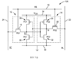
이에 관하여, 도 1a는 제 1 인버터(12) 및 제 2 인버터(14)를 가진 예시적인 SRAM 비트 셀(10A)의 회로도이다. 워드 라인(WL)(16)은 인버터들(12, 14) 양쪽에 커플링한다. 특히, WL(16)은 제 1 통과 게이트(PG) 트랜지스터(18)(PG1)의 게이트를 통해 제 1 인버터(12)에 커플링하고 제 2 PG 트랜지스터(20)(PG2)의 게이트를 통해 제 2 인버터(14)에 커플링한다. 비트 라인(22)은 제 2 PG 트랜지스터(20)의 드레인에 커플링한다. 비트 라인 바(24)는 제 1 PG 트랜지스터(18)의 소스에 커플링한다.[0023]
In this regard, FIG. 1A is a circuit diagram of an exemplary
[0024]
도 1a를 계속 참조하여, 제 1 인버터(12)는 제 1 풀 업(PU: pull up) 트랜지스터(26)(PU1) 및 제 1 풀 다운(PD: pull down) 트랜지스터(28)(PD1)를 포함한다. 제 2 인버터(14)는 제 1 PU 트랜지스터(30)(PU2) 및 제 2 PD 트랜지스터(32)(PD2)를 포함한다. 전압원(VDD)(34)은 제 1 및 제 2 PU 트랜지스터들(26, 30)에 커플링한다. PD 트랜지스터들(28, 32)은 접지(36)에 커플링된다.1A, the
[0025]
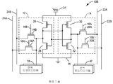
도 1a의 SRAM 비트 셀(10A)이 많은 애플리케이션들에서 사용되지만, SRAM 비트 셀(10A)에 대한 하나의 공통 변형은 다수의 R/W 포트들을 가진 비트 셀이다. 이에 관하여, 도 1b는 다수의 R/W 포트들을 가진 SRAM 비트 셀(10B)을 예시한다. 제 1 비트 라인 바(24A)는 제 1 제 1 PG 트랜지스터(18A)의 소스에 커플링하고 제 2 비트 라인 바(24B)는 제 2 제 1 PG 트랜지스터(18B)의 소스에 커플링한다. 제 1 PG 트랜지스터들(18A, 18B)의 드레인들은 제 1 인버터(12)에 커플링된 공통 노드를 공유한다. 유사하게, 제 1 비트 라인(22A)은 제 1 제 2 PG 트랜지스터(20A)의 소스에 커플링하고 제 2 비트 라인(22B)은 제 2 제 2 PG 트랜지스터(20B)의 소스에 커플링한다. 제 2 PG 트랜지스터들(20A, 20B)의 드레인들은 제 2 인버터(14)에 커플링된 공통 노드를 공유한다. 다수의 기록 라인들(16A, 16B)은 PG 트랜지스터들(18A, 18B, 20A, 20B)에 커플링될 수 있다. 부가적으로, 제 1 판독 트랜지스터들(38)은 제 1 인버터(12)에 커플링될 수 있고, 제 2 판독 트랜지스터들(40)은 제 2 인버터(14)에 커플링될 수 있다. 단지 두 개의 비트 라인들 및 두 개의 비트 라인 바 입력들이 도시되지만, 적당한 PG 트랜지스터가 더 많이 존재할 수 있다는 것이 인식되어야 한다.[0025]
One common variation for the
[0026]
RAM 비트 셀들은, 본질적으로 레지스터 파일의 기본 빌딩 블록들이고 이와 같이, SRAM 비트 셀들(10A, 10B)은 도 2에 예시된 바와 같이 시프트 레지스터(42) 같은 레지스터로 어셈블리될 수 있다. 시프트 레지스터(42)는 네 개의 SRAM 비트 셀들(10(1)-10(4))을 포함하는 네 개의 비트 시프트 레지스터이다. 클럭 신호(44)는 원해지면 각각의 비트 셀에 제공될 수 있다. 데이터는 처음에 라인(46) 내 데이터에 제공된다. 출력들(48(1)-48(4))은 개별 비트 셀들(10(1)-10(4))에 대해 제공된다. 네 개의 비트 시프트 레지스터(42)가 예시되지만, 보다 많은 비트 셀들이 보다 큰 레지스터들로 어셈블리될 수 있다는 것이 인식되어야 한다. 시프트 레지스터가 특정하게 예시되지만, 다양한 구성들의 레지스터들은 가능하고 그 용어가 본원에 사용된 바와 같이 용어 "레지스터 파일" 내에 모두 속한다.[0026]
The RAM bit cells are essentially the basic building blocks of the register file and thus the
[0027] 레지스터들은 액세스하기에 빠른 메모리 블록을 제공하는 컴퓨팅 디바이스들에 유용한 기능을 서빙하고, 레지스터들은 하드 드라이브 같은 보다 느린 메모리에 액세스할 필요를 제거한다. 레지스터들은 산술 논리 유닛(ALU)과 연관될 수 있다. 게다가, 프로세싱 코어에 의해서만 효과적으로 판독될 수 있는 캐시 메모리와 달리, 레지스터들은 판독 및 기록 둘 다를 수행할 수 있고 이는 ALU가 조작되는 데이터를 저장하게 한다. 이들의 과중사용으로 인해, 레지스터들은 도 3a 및 도 3b에 추가로 예시된 바와 같이 ALU와 동일한 집적 회로 내에 빈번하게 포지셔닝된다.[0027] The registers serve functions useful for computing devices that provide a fast memory block to access, and the elimination of the need to access slower memory such as hard drives. The registers may be associated with an arithmetic logic unit (ALU). In addition, unlike cache memories, which can be effectively read only by the processing cores, the registers can perform both reading and writing, which allows the ALU to store the data to be manipulated. Due to their heavy use, the registers are frequently positioned in the same integrated circuit as the ALU, as further illustrated in Figures 3A and 3B.
[0028]
이에 관하여, 도 3a는 ALU(52)를 사용하는 프로세싱 코어를 가진 예시적인 IC(50A)를 예시한다. ALU(52)는 레지스터(54)뿐 아니라 레벨 1(L1) 캐시(56) 및 레벨 2(L2) 캐시(58)와 연관되어 통신한다. 예시적인 실시예에서, ALU(52)는 레지스터(54)를 통해 L1 캐시(56)와 통신한다. 대안적인 실시예에서, ALU(52)는 레지스터(54)를 통한 통과 없이 직접 L1 캐시(56)와 통신할 수 있다. IC(50A)는 RAM(60) 같은 외부 메모리 디바이스들과 통신할 수 있다. 예시적인 실시예에서, IC(50A)는 단일 코어 및 단일 ALU(52)를 가지며, 따라서 레지스터(54)는 단지 단일 ALU(52)를 서빙한다. 그러나, 몇몇 IC들은 단일 코어 및 다수의 ALU(도시되지 않음)를 가질 수 있다. 그런 실시예에서, 레지스터들은 잘 이해될 바와 같이 다양한 ALU에 커플링될 수 있다. 게다가, 커플링 산업은 점점 각각 하나 또는 그 초과의 ALU를 가진 다중-코어 프로세서들에 의존한다.[0028]
In this regard, FIG. 3A illustrates an
[0029]
이에 관하여, 도 3b는 제 1 코어(66) 내의 제 1 ALU(62) 및 제 2 코어(68) 내의 제 2 ALU(64)를 사용하는 다중-코어 프로세서를 포함하는 예시적인 IC(50B)를 예시한다. 상기 주의된 바와 같이, 코어들(66, 68)은 다수의 ALU(도시되지 않음)를 가질 수 있다. ALU들(62, 64)은 공유된 용법을 가능하게 하기 위하여 하나 또는 그 초과의 다중-포트 SRAM 비트셀들(10B)을 가질 수 있는 공유된 레지스터(70)를 협력하여 사용할 수 있다. ALU들(62, 64)이 또한 특정 ALU(62, 64)와 연관된 타이밍 임계 회로들에 대해 기능하는 전용 레지스터들(도시되지 않음)을 가질 수 있다는 것이 인식되어야 한다. ALU들(62, 64)은 잘 이해되는 바와 같이 L1 캐시(72) 및 L2 캐시(74)를 추가로 사용할 수 있다. 상기 주의된 바와 같이, 예시적인 실시예에서, ALU들(62, 64)은 레지스터(70)를 통해 L1 캐시(72)와 통신할 수 있다. IC(50B)는 RAM(76) 같은 외부 메모리와 추가로 통신할 수 있다. 도 1a-도 3b의 논의가 레지스터 내 SRAM 비트셀들의 사용에 집중되지만, L1 또는 L2 캐시 또는 외부 RAM 같은 다른 메모리 블록들이 또한 SRAM 비트셀들로부터 형성될 수 있다는 것이 인식되어야 한다.[0029]
3B illustrates an
[0030]
SRAM 비트 셀들의 이런 일반 사용에 반대하여, IC들을 소형화하기 위한 현재 노력들이 IC들(50A, 50B) 같은 IC 내의 공간 사용에 대한 항상 증가하는 수요들을 수반한다는 것이 인식되어야 한다. 부가적으로, 메모리 수요들이 다중-스레드 프로세서들에서 증가하기 때문에, SRAM 기반 레지스터 파일들의 크기는 증가한다. 레지스터가 커질수록, 레지스터 파일 액세스 동안 보다 큰 레이턴시가 발생한다. 게다가, 비트 셀들의 수가 증가하기 때문에, 주변 논리 영역은 증가하고 레지스터 파일 둘레에 배치된 다른 컴포넌트들에 대한 재타이밍 아크들을 생성할 수 있다. 소형화 염려들에 더하여, 비트 셀들에 대한 VDD를 감소시키는 전력 소비에 관해 염려가 증가하고 있다. VDD가 너무 작게 되면, SNM 및 RWNM은 팩터(factor)들을 제한하게 되고 판독 및 기록 동작들의 전원들을 분리함으로써 최적화될 수 있다. 그 다음 각각의 전압원에 대하여 전도 경로들을 라우팅하는 것은 낮은 전력 시스템에 대해 추가 병목이 이루어지게 하고 레지스터 파일 내에 다수의 전원 레일들을 가지는 것은 추가 영역 페널티(penalty)를 유도한다. 쉽게 이해되는 바와 같이, 이들 문제들은 시너지적으로 서로 공급되고 이는 회로 설계자들에게 어려움들을 유발한다.[0030] In contrast to this general use of SRAM bit cells, it should be appreciated that current efforts to miniaturize ICs involve ever-increasing demands for space usage in ICs such as
[0031] 본 개시는 3DIC의 다수의 티어들에 걸쳐 펼쳐진 레지스터 파일의 상이한 엘리먼트들을 레지스터 파일 코어 셀 설계에 제공함으로써 기술의 현재 상태의 결함들을 치유한다. 3DIC의 티어들에 걸쳐 레지스터 파일을 분할함으로써, 다양한 전력 레일들 및 액세스 라인들에 대한 라우팅은 간략화되고 레지스터의 전체 풋프린트가 감소된다. 풋프린트의 감소는 레이턴시를 감소시키고 재타이밍 아크들의 가능성을 감소시킨다.[0031] The present disclosure cures deficiencies in the current state of the art by providing different elements of the register file expanded across the multiple tiers of the 3DIC to the register file core cell design. By dividing the register file across the tiers of the 3DIC, the routing to the various power rails and access lines is simplified and the overall footprint of the register is reduced. Reducing the footprint reduces latency and reduces the likelihood of re-timing arcs.
[0032]
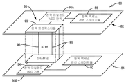
이에 관하여, 도 4는 제 1 티어(82) 및 제 2 티어(84)에 걸쳐 펼쳐진 레지스터 파일(86)을 가진 제 1 티어(82) 및 제 2 티어(84)를 가진 3DIC(80)를 예시한다. 도 4의 예시된 실시예에서, 판독 액세스 관련 스테이지들(88)(판독 액세스를 제공하도록 구성된 프로세서 코어 판독 논리 및 판독 액세스 포트를 포함함) 및 판독 트랜지스터들(90)은 제 1 티어(82)에 포지셔닝되는 반면 기록 액세스 관련 스테이지들(92)(기록 액세스를 제공하도록 구성된 프로세서 코어 기록 논리 및 기록 액세스 포트를 포함함) 및 SRAM 셀(94)의 인버터들은 제 2 티어(84)에 포지셔닝되어, 제 2 티어(84)에 레지스터 파일(86)의 메모리 셀 부분이 포지셔닝된다. 판독 트랜지스터들(90)은 SRAM 셀(94)의 인버터들과 통신한다. 예시적인 실시예에서, 판독 트랜지스터들(90)은 하나 또는 그 초과의 모놀리식 인터티어 비아들(MIV)(96)을 사용하여 SRAM 셀(94)에 커플링된다. 3DIC(80)의 다수의 티어들(82, 84)에 걸쳐 레지스터 파일(86)을 분할함으로써 레지스터 파일(86)의 전체 풋프린트는 2차원 레지스터 파일에 비교될 때 감소된다. 게다가, SRAM 셀(94)로부터 판독 트랜지스터들(90)을 분리함으로써, 라우팅 전압 레일들 및 다수의 액세스 포트들에 관한 라우팅 문제들은 쉬워진다. 따라서, 예시된 바와 같이 제 1 전력 아일랜드(island)(95A)는 제 1 티어(82) 상에 제공되고 VDD _READ를 판독 트랜지스터들(90) 및 판독 액세스 관련 스테이지들(88) 내의 적당한 엘리먼트들에 제공한다. 마찬가지로, 제 2 전력 아일랜드(95B)는 제 2 티어(84) 상에 제공되고 VDD _WRITE를 SRAM 셀(94) 및 기록 액세스 관련 스테이지들(92) 내의 적당한 엘리먼트들에 제공한다. 별개의 전압 레일들의 포함은, 메모리 비트의 부적당한 플립들이 회피되도록 SNM을 완화시키는 것을 돕는다. 통상적인 SRAM 셀(94)이 대략 0.1 내지 0.09 제곱 미크론들인 것이 주의된다. 통상적인 관통 실리콘 비아(TSV)는 약 5 미크론들의 직경 - 즉, SRAM 셀(94)보다 훨씬 큰 직경을 가진다. MIV(96)는 TSV보다 훨씬 작고, 대략 0.05 미크론들이며 따라서 TSV 대신 MIV(96)의 사용은 다수의 티어들(82, 84)에 걸쳐 레지스터 파일(86)을 분할할 때 풋프린트 절약들을 보존한다. 본원에 사용된 바와 같이 판독을 위한 수단은 판독 액세스 포트 및 등가물들을 지정하기 위하여 사용된다. 마찬가지로, 본원에 사용된 바와 같이, 기록을 위한 수단은 기록 액세스 포트 및 등가물들을 지정하기 위하여 사용된다.4 shows a 3DIC 80 having a
[0033] MIV의 개념은 이로써 참조에 의해 포함된 IEEE/ACM Asia South Pacific Design Automation Conference, 2013; pp. 681-686의 회의에서 Shreedpad Panth 등에 의한 명칭이 "High-Density Integration of Functional Modules Using Monolithic 3D-IC Technology"인 서류에서 공개되었다.[0033] The concept of MIV is described in IEEE / ACM Asia Pacific Design Automation Conference, 2013, hereby incorporated by reference. pp. At the meeting of 681-686, the name Shreedpad Panth et al. Was disclosed in a document entitled " High-Density Integration of Functional Modules Using Monolithic 3D-IC Technology ".
[0034]
도 4는 제 2 티어(84) 상에 기록 액세스 관련 스테이지들(92)을 예시하는 반면 다른 예시적인 실시예에서, 기록 액세스 관련 스테이지들(92)은 제 1 티어(82) 상에 있을 수 있다. 만약 기록 액세스 관련 스테이지들(92)이 제 1 티어(82) 상에 있다면, MIV들(96)은 기록 액세스 관련 테이지들(92)을 SRAM 셀(94)에 커플링하기 위하여 사용될 수 있다.[0034]
Figure 4 illustrates write access related
[0035]
도 5는 MIV(98)와 커플링된 제 1 티어(82) 및 제 2 티어(84)를 가진 3DIC(80)의 단면도를 예시한다. 엘리먼트들(100)은 PMOS 또는 NMOS 트랜지스터들일 수 있는 하나 또는 그 초과의 트랜지스터들을 포함하는 제 1 티어(82) 내에 포지셔닝된다. 엘리먼트들(102)은 마찬가지로 PMOS 또는 NMOS 트랜지스터들일 수 있는 하나 또는 그 초과의 트랜지스터들을 포함하는 제 2 티어(84) 내에 포지셔닝된다. 엘리먼트들(100)은 비아들(108)에 의해 커플링된 하나 또는 그 초과의 금속 층들(104, 106)을 포함할 수 있다. 엘리먼트들(102)은 비아들(114)에 의해 커플링된 하나 또는 그 초과의 금속 층들(110, 112)을 포함할 수 있다. 금속 층들(104, 106, 110, 112)은 수평 상호연결들을 제공하고 3DIC 내의 전도 라우팅 경로들을 가능하게 한다. 종래의 상호연결 비아와 대략 동일한 크기인 작은 MIV 크기는 매우 고밀도의 인터-티어 연결들을 생성하여, 가능하고 경제적으로 실행 가능한 상이한 티어들에 판독 및 기록 포트들의 분리를 형성한다.[0035]
5 illustrates a cross-sectional view of a
[0036]
다중-티어 레지스터 파일(86)은 특히 다중-코어 프로세서들에 매우 적당하다. 즉, 다중-티어 레지스터 파일(86)은 도 3b에 개략적으로 도시된 다중-코어 IC(50B) 같은 다중-코어 프로세서의 코어들 사이에서 공유되고 코어들이 3DIC(80) 내의 상이한 티어들 상에 배치되게 할 수 있다. 포지셔닝에서 그런 융통성은 전도 경로들을 라우팅하고, 레이턴시를 감소시키고 그렇지 않으면 다중-코어 프로세서들의 성능을 개선시킴에 있어 설계자들을 돕는다.[0036]
The
[0037] 본원에 개시된 실시예들에 따른 3DIC들에서 레지스터 파일들은 임의의 프로세서 기반 디바이스에 제공되거나 통합될 수 있다. 제한 없이 예들은 셋톱 박스, 엔터테인먼트 유닛, 네비게이션 디바이스, 통신 디바이스, 고정 위치 데이터 유닛, 모바일 위치 데이터 유닛, 모바일 폰, 셀룰러 폰, 컴퓨터, 휴대용 컴퓨터, 데스크톱 컴퓨터, 개인용 휴대 정보 단말기(PDA), 모니터, 컴퓨터 모니터, 텔레비전, 튜너, 라디오, 위성 라디오, 뮤직 플레이어, 디지털 뮤직 플레이어, 휴대용 뮤직 플레이어, 디지털 비디오 플레이어, 비디오 플레이어, 디지털 비디오 디스크(DVD) 플레이어, 및 휴대용 디지털 비디오 플레이어를 포함한다.[0037] Register files in 3DICs according to embodiments disclosed herein may be provided or integrated into any processor-based device. Examples include, but are not limited to, a set top box, an entertainment unit, a navigation device, a communication device, a fixed location data unit, a mobile location data unit, a mobile phone, a cellular phone, a computer, a portable computer, a desktop computer, a personal digital assistant A computer monitor, a television, a tuner, a radio, a satellite radio, a music player, a digital music player, a portable music player, a digital video player, a video player, a digital video disk (DVD) player, and a portable digital video player.
[0038]
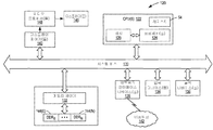
이에 관하여, 도 6은 도 4 및 도 5에 예시된 3DIC의 레지스터 파일들을 이용할 수 있는 프로세서 기반 시스템(120)의 예를 예시한다. 이 예에서, 프로세서 기반 시스템(120)은 각각 하나 또는 그 초과의 프로세서들(124)을 포함하는 하나 또는 그 초과의 중앙 프로세싱 유닛(CPU)들(122)을 포함한다. CPU(들)(122)는 레지스터(54)를 포함할 수 있고 및/또는 마스터 디바이스일 수 있다. CPU(들)(122)는 일시적으로 저장된 데이터에 빠른 액세스를 위하여 프로세서(들)(124)에 커플링된 캐시 메모리(126)를 가질 수 있다. CPU(들)(122)은 시스템 버스(130)에 커플링되고 프로세서 기반 시스템(120)에 포함된 마스터 디바이스들 및 슬레이브 디바이스들을 상호 커플링할 수 있다. 잘 알려진 바와 같이, CPU(들)(122)은 시스템 버스(130)를 통해 어드레스, 제어, 및 데이터 정보를 교환함으로써 이들 다른 디바이스들과 통신한다. 예를 들어, CPU(들)(122)는 슬레이브 디바이스의 예로서 메모리 제어기(132)에 버스 트랜잭션 요청들을 통신할 수 있다. 비록 도 6에 예시되지 않지만, 다수의 시스템 버스들(130)이 제공될 수 있고, 각각의 시스템 버스(130)는 상이한 구조를 구성한다.[0038]
In this regard, FIG. 6 illustrates an example of a processor-based
[0039]
다른 마스터 및 슬레이브 디바이스들은 시스템 버스(130)에 연결될 수 있다. 도 6에 예시된 바와 같이, 이들 디바이스들은 메모리 제어기(132), 하나 또는 그 초과의 입력 디바이스들(134), 하나 또는 그 초과의 출력 디바이스들(136), 하나 또는 그 초과의 네트워크 인터페이스 디바이스들(138), 및 하나 또는 그 초과의 디스플레이 제어기들(140)을 예들로서 포함할 수 있다. 입력 디바이스(들)(134)는 입력 키들, 스위치들, 음성 프로세서들, 등(그러나 이들로 제한되지 않음)을 포함하는 임의의 타입의 입력 디바이스를 포함할 수 있다. 출력 디바이스(들)(136)는 오디오, 비디오, 다른 시각 표시기들, 등(그러나 이들로 제한되지 않음)을 포함하는 임의의 타입의 출력 디바이스를 포함할 수 있다. 네트워크 인터페이스 디바이스(들)(138)는 네트워크(142)에 그리고 네트워크(142)로부터 데이터의 교환을 허용하도록 구성된 임의의 디바이스들일 수 있다. 네트워크(142)는 무선 네트워크, 사설 또는 공용 네트워크, 로컬 영역 네트워크(LAN), WLAN(wide local area network), 및 인터넷(그러나 이들로 제한되지 않음)을 포함하는 임의의 타입의 네트워크일 수 있다. 네트워크 인터페이스 디바이스(들)(138)는 원해진 임의의 타입의 통신 프로토콜을 지원하도록 구성될 수 있다. 메모리 제어기(132)는 하나 또는 그 초과의 메모리 유닛들(144(0-N))을 포함할 수 있다.[0039]
Other master and slave devices may be coupled to the
[0040]
CPU(들)(122)는 또한 하나 또는 그 초과의 디스플레이들(146)에 전송된 정보를 제어하기 위하여 시스템 버스(130)를 통해 디스플레이 제어기(들)(140)에 액세스하도록 구성될 수 있다. 디스플레이 제어기(들)(140)는 디스플레이(들)(146)에 적당한 포맷으로 디스플레이될 정보를 프로세싱하는 하나 또는 그 초과의 비디오 프로세서들(148)을 통해 디스플레이될 정보를 디스플레이(들)(146)에 전송한다. 디스플레이(들)(146)는 음극선관(CRT), 액정 디스플레이(LCD), 플라즈마 디스플레이, 등(그러나 이들로 제한되지 않음)을 포함하는 임의의 타입의 디스플레이를 포함할 수 있다.[0040]
The CPU (s) 122 may also be configured to access the display controller (s) 140 via the
[0041] 당업자들은, 본원에 개시된 실시예들과 관련하여 설명된 다양한 예시적 논리 블록들, 모듈들, 회로들, 및 알고리즘이 전자 하드웨어, 메모리 또는 다른 컴퓨터 판독가능 매체에 저장되고 프로세서 또는 다른 프로세싱 디바이스에 의해 실행되는 명령들, 또는 둘의 결합들로서 구현될 수 있다는 것을 추가로 인식할 것이다. 본원에 개시된 조정자(arbiter)들, 마스터 디바이스들, 및 슬레이브 디바이스들은 예들로서 임의의 회로, 하드웨어 컴포넌트, IC, 또는 IC 칩에 이용될 수 있다. 본원에 개시된 메모리는 임의의 타입 및 크기의 메모리일 수 있고 원해진 임의의 타입의 정보를 저장하도록 구성될 수 있다. 이런 교환성을 명확하게 예시하기 위하여, 다양한 예시적 컴포넌트들, 블록들, 모듈들, 회로들, 및 단계들은 일반적으로 그들의 기능성 측면에서 상기 설명되었다. 그런 기능성이 구현되는 방법은 특정 애플리케이션, 설계 선택들, 및/또는 전체 시스템에 부과된 설계 제약들에 따른다. 당업자들은 각각의 특정 애플리케이션에 대해 가변하는 방식으로 설명된 기능성을 구현할 수 있지만, 그런 구현 판정들은 본 개시의 범위에서 벗어남을 유발함으로서 해석되지 않아야 한다.[0041] Those skilled in the art will appreciate that the various illustrative logical blocks, modules, circuits, and algorithms described in connection with the embodiments disclosed herein may be implemented within a computer-readable medium, stored in an electronic hardware, memory, or other computer- Executable instructions, or a combination of the two. The arbiters, master devices, and slave devices disclosed herein may be used in any circuit, hardware component, IC, or IC chip as an example. The memory disclosed herein can be any type and size of memory and can be configured to store any type of information desired. To clearly illustrate this interchangeability, various illustrative components, blocks, modules, circuits, and steps have been described above generally in terms of their functionality. The manner in which such functionality is implemented depends upon the particular application, design choices, and / or design constraints imposed on the overall system. Skilled artisans may implement the described functionality in varying ways for each particular application, but such implementation decisions should not be interpreted as causing a departure from the scope of the present disclosure.
[0042] 본원에 개시된 실시예들과 관련하여 설명된 다양한 예시적 논리 블록들, 모듈들, 및 회로들은 프로세서, 디지털 신호 처리기(DSP), 주문형 집적회로(ASIC), 필드 프로그램어블 게이트 어레이(FPGA) 또는 다른 프로그램어블 논리 디바이스, 이산 게이트 또는 트랜지스터 논리, 이산 하드웨어 컴포넌트들, 또는 본원에 설명된 기능들을 수행하도록 설계된 이들의 임의의 결합으로 구현 또는 수행될 수 있다. 프로세서는 마이크로프로세서 일 수 있지만, 대안으로, 프로세서는 임의의 종래 프로세서, 제어기, 마이크로 제어기, 또는 상태 머신일 수 있다. 프로세서는 또한, 컴퓨팅 디바이스들의 결합, 예를 들어 DSP 및 마이크로프로세서, 복수의 마이크로프로세서들, DSP 코어와 결합된 하나 또는 그 초과의 마이크로프로세서들, 또는 임의의 다른 그런 구성과의 결합으로서 구현될 수 있다.[0042] The various illustrative logical blocks, modules, and circuits described in connection with the embodiments disclosed herein may be implemented or performed with a digital signal processor (DSP), an application specific integrated circuit (ASIC), a field programmable gate array Programmable logic devices, discrete gate or transistor logic, discrete hardware components, or any combination thereof designed to perform the functions described herein. A processor may be a microprocessor, but, in the alternative, the processor may be any conventional processor, controller, microcontroller, or state machine. A processor may also be implemented as a combination of computing devices, e.g., a combination of a DSP and a microprocessor, a plurality of microprocessors, one or more microprocessors in conjunction with a DSP core, or any other such configuration have.
[0043] 본원에 개시된 실시예들은 하드웨어, 하드웨어에 저장된 명령들로 구현될 수 있고 예를 들어 랜덤 액세스 메모리(RAM), 플래시 메모리, 판독 전용 메모리(ROM), 전기적 프로그램어블 ROM(EPROM), 전기적 소거 가능한 프로그램어블 ROM(EEPROM), 레지스터들, 하드디스크, 제거 가능 디스크, CD-ROM, 또는 기술 분야에서 알려진 임의의 다른 형태의 컴퓨터 판독가능 매체에 상주할 수 있다. 예시적인 스토리지 매체는 프로세서와 커플링되어, 프로세서는 스토리지 매체로부터 정보를 판독하여 스토리지 매체에 정보를 기록할 수 있다. 대안으로, 스토리지 매체는 프로세서의 구성요소일 수 있다. 프로세서 및 스토리지 매체는 ASIC에 상주할 수 있다. ASIC는 원격 스테이션에 상주할 수 있다. 대안으로, 프로세서 및 스토리지 매체는 원격 스테이션, 기지국, 또는 서버에 이산 컴포넌트로서 상주할 수 있다. [0043] The embodiments disclosed herein may be implemented in hardware, hardware-based instructions, and may include, for example, random access memory (RAM), flash memory, read only memory (ROM), electrically programmable ROM (EPROM) (EEPROM), registers, a hard disk, a removable disk, a CD-ROM, or any other form of computer readable medium known in the art. An exemplary storage medium is coupled to the processor such that the processor can read information from, and write information to, the storage medium. Alternatively, the storage medium may be a component of the processor. The processor and storage medium may reside in an ASIC. The ASIC may reside in a remote station. Alternatively, the processor and storage medium may reside as discrete components in a remote station, base station, or server.
[0044] 또한 본원의 예시적인 실시예들의 임의의 실시예에 설명된 동작 단계들이 예들 및 논의를 제공하기 위하여 설명되는 것이 주의된다. 설명된 동작들은 예시된 시퀀스들과 상이한 다수의 시퀀스들로 수행될 수 있다. 게다가, 단일 동작 단계에서 설명된 동작들은 실제로 다수의 상이한 단계들에서 수행될 수 있다. 부가적으로, 예시적인 실시예들에서 논의된 하나 또는 그 초과의 동작 단계들은 결합될 수 있다. 흐름도들에서 예시된 동작 단계들이 당업자에게 쉽게 명백할 바와 같이 다수의 상이한 수정들에 영향을 받을 수 있다는 것이 이해될 것이다. 당업자들은 또한, 정보 및 신호들이 다양한 상이한 기술들 및 기법들 중 임의의 것을 사용하여 표현될 수 있다는 것을 이해할 것이다. 예를 들어, 상기 설명을 통해 참조될 수 있는 데이터, 명령들, 커맨드들, 정보, 신호들, 비트들, 심볼들, 및 칩들은 전압들, 전류들, 전자기 파들, 자기장들 또는 입자들, 광학 필드들 또는 입자들, 또는 이들의 임의의 결합에 의해 표현될 수 있다.[0044] It is also noted that the operational steps described in any of the embodiments of the exemplary embodiments herein are described to provide examples and discussion. The described operations may be performed with a plurality of sequences different from the exemplified sequences. In addition, the operations described in the single operation step may actually be performed in a number of different steps. Additionally, one or more of the operational steps discussed in the exemplary embodiments may be combined. It will be appreciated that the operating steps illustrated in the flowcharts can be affected by a number of different modifications as will be readily apparent to those skilled in the art. Those skilled in the art will also appreciate that information and signals may be represented using any of a variety of different technologies and techniques. For example, data, instructions, commands, information, signals, bits, symbols, and chips that may be referenced throughout the above description may include voltages, currents, electromagnetic waves, magnetic fields or particles, Fields, or particles, or any combination thereof.
[0045] 본 개시의 이전 설명은 당업자가 본 개시를 만들거나 이용하게 하도록 제공된다. 본 개시에 대한 다양한 변형들은 당업자들에게 쉽게 명백할 것이며, 본원에 정의된 일반적인 원리들은 본 개시의 사상 또는 범위를 벗어남이 없이 다른 변형들에 적용될 수 있다. 따라서, 본 개시는 본원에 설명된 예들 및 설계들로 한정되는 것이 아니라, 본원에 개시된 원리들 및 신규한 특징들에 일치하는 최광의의 범위에 부합되도록 의도된다.[0045] The previous description of the disclosure is provided to enable any person skilled in the art to make or use the disclosure. Various modifications to the disclosure will be readily apparent to those skilled in the art, and the generic principles defined herein may be applied to other variations without departing from the spirit or scope of the disclosure. Accordingly, the disclosure is not intended to be limited to the examples and designs described herein but is to be accorded the widest scope consistent with the principles and novel features disclosed herein.
Claims (19)
3D 집적 회로(IC)(3DIC)의 제 1 티어(tier)에 배치된 메모리 셀;
상기 3DIC의 제 2 티어에 배치된 적어도 하나의 판독 액세스 포트 ― 상기 적어도 하나의 판독 액세스 포트는 상기 메모리 셀에 판독 액세스를 제공하도록 구성됨 ―; 및
상기 적어도 하나의 판독 액세스 포트를 상기 메모리 셀에 커플링하는 적어도 하나의 모놀로식 인터티어 비아(MIV: monolithic intertier via)
를 포함하는,
3차원(3D) 메모리 블록.As a three-dimensional (3D) memory block,
A memory cell arranged in a first tier of a 3D integrated circuit (IC) (3DIC);
At least one read access port disposed in a second tier of the 3D IC, the at least one read access port configured to provide read access to the memory cell; And
At least one monolithic intertier via (MIV) coupling said at least one read access port to said memory cell;
/ RTI >
Three-dimensional (3D) memory blocks.
정적 랜덤 액세스 메모리(SRAM) 블록으로 구성된,
3차원(3D) 메모리 블록.The method according to claim 1,
Consisting of a static random access memory (SRAM) block,
Three-dimensional (3D) memory blocks.
상기 3DIC의 상기 제 1 티어에 배치된 적어도 하나의 기록 액세스 포트를 더 포함하고, 상기 적어도 하나의 기록 액세스 포트는 메모리 셀에 기록 액세스를 제공하도록 구성되는,
3차원(3D) 메모리 블록.The method according to claim 1,
Further comprising at least one write access port disposed in the first tier of the 3D IC, wherein the at least one write access port is configured to provide write access to a memory cell,
Three-dimensional (3D) memory blocks.
상기 3DIC의 상기 제 2 티어에 배치된 적어도 하나의 기록 액세스 포트를 더 포함하고, 상기 적어도 하나의 기록 액세스 포트는 상기 적어도 하나의 MIV를 통해 상기 메모리 셀에 기록 액세스를 제공하도록 구성되는,
3차원(3D) 메모리 블록.The method according to claim 1,
Further comprising at least one write access port disposed in the second tier of the 3D IC, wherein the at least one write access port is configured to provide write access to the memory cell via the at least one MIV.
Three-dimensional (3D) memory blocks.
상기 3DIC의 상기 제 1 티어에 배치된 프로세서 코어 기록 논리 ― 상기 프로세서 코어 기록 논리는 상기 메모리 셀의 적어도 하나의 기록 포트에 기록 요청들을 제공하도록 구성됨 ―; 및
상기 3DIC의 제 2 티어에 배치된 프로세서 코어 판독 논리 ― 상기 프로세서 코어 판독 논리는 상기 메모리 셀의 상기 적어도 하나의 판독 액세스 포트에 판독 액세스들을 제공하도록 구성됨―
를 더 포함하는,
3차원(3D) 메모리 블록.The method according to claim 1,
A processor core write logic disposed in the first tier of the 3DIC, the processor core write logic being configured to provide write requests to at least one write port of the memory cell; And
Processor core read logic disposed in a second tier of the 3DIC, wherein the processor core read logic is configured to provide read accesses to the at least one read access port of the memory cell,
≪ / RTI >
Three-dimensional (3D) memory blocks.
상기 3DIC의 상기 제 1 티어에 배치된 제 1 전압이 공급되는 제 1 전압 레일(rail) ― 상기 제 1 전압 레일은 상기 제 1 전압을 상기 메모리 셀에 공급하도록 구성됨 ―; 및
상기 제 1 전압 레일에 공급된 상기 제 1 전압보다 낮은 제 2 전압이 공급되는 제 2 전압 레일 ― 상기 제 2 전압 레일은 상기 3DIC의 상기 제 2 티어에 배치되고 상기 제 2 전압을 상기 적어도 하나의 판독 액세스 포트에 공급하도록 구성됨 ―
을 더 포함하는,
3차원(3D) 메모리 블록.The method according to claim 1,
A first voltage rail to which a first voltage disposed in the first tier of the 3DIC is supplied, the first voltage rail configured to supply the first voltage to the memory cell; And
A second voltage rail to which a second voltage lower than the first voltage supplied to the first voltage rail is supplied, the second voltage rail being arranged in the second tier of the 3DIC and the second voltage being supplied to the at least one Read access port.
≪ / RTI >
Three-dimensional (3D) memory blocks.
반도체 다이에 통합되는,
3차원(3D) 메모리 블록.The method according to claim 1,
Integrated into a semiconductor die,
Three-dimensional (3D) memory blocks.
상기 3D 메모리 블록이 통합되는, 셋톱 박스, 엔터테인먼트 유닛, 네비게이션 디바이스, 통신 디바이스, 고정 위치 데이터 유닛, 모바일 위치 데이터 유닛, 모바일 폰, 셀룰러 폰, 컴퓨터, 휴대용 컴퓨터, 데스크톱 컴퓨터, 개인용 휴대 정보 단말기(PDA), 모니터, 컴퓨터 모니터, 텔레비전, 튜너, 라디오, 위성 라디오, 뮤직 플레이어, 디지털 뮤직 플레이어, 휴대용 뮤직 플레이어, 디지털 비디오 플레이어, 비디오 플레이어, 디지털 비디오 디스크(DVD) 플레이어, 및 휴대용 디지털 비디오 플레이어로 이루어진 그룹으로부터 선택된 디바이스를 더 포함하는,
3차원(3D) 메모리 블록.The method according to claim 1,
A set top box, an entertainment unit, a navigation device, a communication device, a fixed position data unit, a mobile position data unit, a mobile phone, a cellular phone, a computer, a portable computer, a desktop computer, a personal digital assistant ), A monitor, a computer monitor, a television, a tuner, a radio, a satellite radio, a music player, a digital music player, a portable music player, a digital video player, a video player, a digital video disk (DVD) player, ≪ / RTI >
Three-dimensional (3D) memory blocks.
상기 3D 메모리 블록은 집적 회로 내에 레지스터를 포함하는,
3차원(3D) 메모리 블록.The method according to claim 1,
Wherein the 3D memory block comprises a register in an integrated circuit,
Three-dimensional (3D) memory blocks.
상기 3D 메모리 블록은 집적 회로 내에 캐시 메모리를 포함하는,
3차원(3D) 메모리 블록.The method according to claim 1,
Wherein the 3D memory block comprises a cache memory in an integrated circuit,
Three-dimensional (3D) memory blocks.
3D 집적 회로(IC)(3DIC)의 제 1 티어에 배치된 메모리 셀;
상기 3DIC의 제 2 티어에 배치된 판독을 위한 적어도 하나의 수단 ― 상기 판독을 위한 적어도 하나의 수단은 상기 메모리 셀에 판독 액세스를 제공하도록 구성됨 ―; 및
상기 판독을 위한 적어도 하나의 수단을 상기 메모리 셀에 커플링하는 적어도 하나의 모놀로식 인터티어 비아(MIV)
를 포함하는,
3차원(3D) 메모리 블록.As a three-dimensional (3D) memory block,
A memory cell disposed in a first tier of a 3D integrated circuit (IC) (3DIC);
At least one means for reading disposed in a second tier of the 3DIC, at least one means for said reading being configured to provide read access to said memory cell; And
At least one monolithic via via (MIV) coupling said at least one means for said reading to said memory cell,
/ RTI >
Three-dimensional (3D) memory blocks.
상기 3DIC의 상기 제 1 티어에 배치된 상기 기록을 위한 적어도 하나의 수단을 더 포함하고, 상기 기록을 위한 적어도 하나의 수단은 상기 메모리 셀에 기록 액세스를 제공하도록 구성되는,
3차원(3D) 메모리 블록.12. The method of claim 11,
At least one means for said writing arranged in said first tier of said 3D IC, wherein at least one means for said writing is configured to provide write access to said memory cell,
Three-dimensional (3D) memory blocks.
3D 집적 회로(IC)(3DIC)의 제 1 티어를 형성하는 단계;
상기 3DIC의 상기 제 1 티어 내에 메모리 셀을 형성하는 단계;
상기 3DIC의 제 2 티어를 형성하는 단계;
상기 3DIC의 제 2 티어 내에 적어도 하나의 판독 액세스 포트를 형성하는 단계 ― 상기 적어도 하나의 판독 액세스 포트는 상기 메모리 셀에 판독 액세스를 제공하도록 구성됨 ―; 및
적어도 하나의 모놀로식 인터티어 비아(MIV)를 사용하여 상기 적어도 하나의 판독 액세스 포트를 상기 메모리 셀에 커플링하는 단계
를 포함하는,
3차원(3D) 메모리 블록을 형성하는 방법.A method of forming a three-dimensional (3D) memory block,
Forming a first tier of a 3D integrated circuit (IC) (3DIC);
Forming a memory cell in the first tier of the 3DIC;
Forming a second tier of the 3DIC;
Forming at least one read access port in a second tier of the 3D IC, the at least one read access port being configured to provide read access to the memory cell; And
Coupling said at least one read access port to said memory cell using at least one monolithic interconnect via (MIV)
/ RTI >
A method for forming a three-dimensional (3D) memory block.
상기 3DIC의 상기 제 1 티어 상에 적어도 하나의 기록 액세스 포트를 형성하는 단계를 더 포함하고, 상기 적어도 하나의 기록 액세스 포트는 상기 메모리 셀에 기록 액세스를 제공하도록 구성되는,
3차원(3D) 메모리 블록을 형성하는 방법.14. The method of claim 13,
Further comprising: forming at least one write access port on the first tier of the 3D IC, wherein the at least one write access port is configured to provide write access to the memory cell,
A method for forming a three-dimensional (3D) memory block.
레지스터로서 동작하도록 상기 메모리 셀을 구성하는 단계를 더 포함하는,
3차원(3D) 메모리 블록을 형성하는 방법.14. The method of claim 13,
≪ / RTI > further comprising configuring the memory cell to operate as a register,
A method for forming a three-dimensional (3D) memory block.
상기 메모리 셀을 사용하여 SRAM 블록을 형성하는 단계를 더 포함하는,
3차원(3D) 메모리 블록을 형성하는 방법.14. The method of claim 13,
Further comprising forming an SRAM block using the memory cell.
A method for forming a three-dimensional (3D) memory block.
상기 3DIC의 상기 제 2 티어 내에 적어도 하나의 기록 액세스 포트를 형성하는 단계를 더 포함하고, 상기 적어도 하나의 기록 액세스 포트는 상기 적어도 하나의 MIV를 통해 상기 메모리 셀에 기록 액세스를 제공하도록 구성되는,
3차원(3D) 메모리 블록을 형성하는 방법.14. The method of claim 13,
Further comprising forming at least one write access port in the second tier of the 3DIC, wherein the at least one write access port is configured to provide write access to the memory cell via the at least one MIV.
A method for forming a three-dimensional (3D) memory block.
상기 3DIC의 상기 제 1 티어 내에 프로세서 코어 기록 논리를 형성하는 단계 ― 상기 프로세서 코어 기록 논리는 상기 메모리 셀의 적어도 하나의 기록 포트에 기록 요청들을 제공하도록 구성됨 ―; 및
상기 3DIC의 상기 제 2 티어 내에 프로세서 코어 판독 논리를 형성하는 단계 ― 상기 프로세서 코어 판독 논리는 상기 메모리 셀의 상기 적어도 하나의 판독 액세스 포트에 판독 액세스들을 제공하도록 구성됨 ―
을 더 포함하는,
3차원(3D) 메모리 블록을 형성하는 방법.14. The method of claim 13,
Forming processor core write logic in the first tier of the 3DIC, wherein the processor core write logic is configured to provide write requests to at least one write port of the memory cell; And
Forming processor core read logic in the second tier of the 3D IC, the processor core read logic being configured to provide read accesses to the at least one read access port of the memory cell,
≪ / RTI >
A method for forming a three-dimensional (3D) memory block.
상기 3DIC의 상기 제 1 티어 내에 제 1 전압 레일을 형성하는 단계 ― 상기 제 1 전압 레일은 제 1 전압을 상기 메모리 셀에 공급하도록 구성됨 ―; 및
상기 3DIC의 상기 제 2 티어 내에 제 2 전압 레일을 형성하는 단계 ― 상기 제 2 전압 레일은 제 2 전압을 상기 적어도 하나의 판독 액세스 포트에 공급하도록 구성됨 ―
을 더 포함하는,
3차원(3D) 메모리 블록을 형성하는 방법.14. The method of claim 13,
Forming a first voltage rail in the first tier of the 3DIC, the first voltage rail configured to supply a first voltage to the memory cell; And
Forming a second voltage rail in the second tier of the 3D IC, the second voltage rail configured to supply a second voltage to the at least one read access port,
≪ / RTI >
A method for forming a three-dimensional (3D) memory block.
Applications Claiming Priority (5)
| Application Number | Priority Date | Filing Date | Title |
|---|---|---|---|
| US201361800220P | 2013-03-15 | 2013-03-15 | |
| US61/800,220 | 2013-03-15 | ||
| US13/939,274 | 2013-07-11 | ||
| US13/939,274 US9171608B2 (en) | 2013-03-15 | 2013-07-11 | Three-dimensional (3D) memory cell separation among 3D integrated circuit (IC) tiers, and related 3D integrated circuits (3DICS), 3DIC processor cores, and methods |
| PCT/US2014/022929 WO2014150317A1 (en) | 2013-03-15 | 2014-03-11 | Three-dimensional (3d) memory cell with read/write ports and access logic on different tiers of the integrated circuit |
Related Child Applications (1)
| Application Number | Title | Priority Date | Filing Date |
|---|---|---|---|
| KR1020167035866A Division KR20170000397A (en) | 2013-03-15 | 2014-03-11 | Three-dimensional(3d) memory cell with read/write ports and access logic on different tiers of the integrated circuit |
Publications (1)
| Publication Number | Publication Date |
|---|---|
| KR20150132371A true KR20150132371A (en) | 2015-11-25 |
Family
ID=51526452
Family Applications (2)
| Application Number | Title | Priority Date | Filing Date |
|---|---|---|---|
| KR1020167035866A KR20170000397A (en) | 2013-03-15 | 2014-03-11 | Three-dimensional(3d) memory cell with read/write ports and access logic on different tiers of the integrated circuit |
| KR1020157029081A KR20150132371A (en) | 2013-03-15 | 2014-03-11 | Three-dimensional(3d) memory cell with read/write ports and access logic on different tiers of the integrated circuit |
Family Applications Before (1)
| Application Number | Title | Priority Date | Filing Date |
|---|---|---|---|
| KR1020167035866A KR20170000397A (en) | 2013-03-15 | 2014-03-11 | Three-dimensional(3d) memory cell with read/write ports and access logic on different tiers of the integrated circuit |
Country Status (6)
| Country | Link |
|---|---|
| US (2) | US9171608B2 (en) |
| EP (1) | EP2973706B1 (en) |
| JP (2) | JP6309608B2 (en) |
| KR (2) | KR20170000397A (en) |
| CN (1) | CN105144381B (en) |
| WO (1) | WO2014150317A1 (en) |
Families Citing this family (32)
| Publication number | Priority date | Publication date | Assignee | Title |
|---|---|---|---|---|
| US9064077B2 (en) | 2012-11-28 | 2015-06-23 | Qualcomm Incorporated | 3D floorplanning using 2D and 3D blocks |
| US8984463B2 (en) | 2012-11-28 | 2015-03-17 | Qualcomm Incorporated | Data transfer across power domains |
| US9536840B2 (en) | 2013-02-12 | 2017-01-03 | Qualcomm Incorporated | Three-dimensional (3-D) integrated circuits (3DICS) with graphene shield, and related components and methods |
| US9041448B2 (en) | 2013-03-05 | 2015-05-26 | Qualcomm Incorporated | Flip-flops in a monolithic three-dimensional (3D) integrated circuit (IC) (3DIC) and related methods |
| US9177890B2 (en) | 2013-03-07 | 2015-11-03 | Qualcomm Incorporated | Monolithic three dimensional integration of semiconductor integrated circuits |
| US9171608B2 (en) | 2013-03-15 | 2015-10-27 | Qualcomm Incorporated | Three-dimensional (3D) memory cell separation among 3D integrated circuit (IC) tiers, and related 3D integrated circuits (3DICS), 3DIC processor cores, and methods |
| US9418985B2 (en) * | 2013-07-16 | 2016-08-16 | Qualcomm Incorporated | Complete system-on-chip (SOC) using monolithic three dimensional (3D) integrated circuit (IC) (3DIC) technology |
| US9524920B2 (en) * | 2013-11-12 | 2016-12-20 | Taiwan Semiconductor Manufacturing Co., Ltd. | Apparatus and method of three dimensional conductive lines |
| US9123721B2 (en) * | 2013-11-22 | 2015-09-01 | Qualcomm Incorporated | Placement of monolithic inter-tier vias (MIVs) within monolithic three dimensional (3D) integrated circuits (ICs) (3DICs) using clustering to increase usable whitespace |
| US9256246B1 (en) * | 2015-01-29 | 2016-02-09 | Qualcomm Incorporated | Clock skew compensation with adaptive body biasing in three-dimensional (3D) integrated circuits (ICs) (3DICs) |
| US9537471B2 (en) * | 2015-02-09 | 2017-01-03 | Qualcomm Incorporated | Three dimensional logic circuit |
| US9691695B2 (en) * | 2015-08-31 | 2017-06-27 | Taiwan Semiconductor Manufacturing Company, Ltd. | Monolithic 3D integration inter-tier vias insertion scheme and associated layout structure |
| US20190148286A1 (en) * | 2015-09-21 | 2019-05-16 | Monolithic 3D Inc. | Multi-level semiconductor device and structure with memory |
| US20200194416A1 (en) * | 2015-09-21 | 2020-06-18 | Monolithic 3D Inc. | Method to produce a multi-level semiconductor memory device and structure |
| US9754660B2 (en) * | 2015-11-19 | 2017-09-05 | Samsung Electronics Co., Ltd. | Semiconductor device |
| CN105304123B (en) * | 2015-12-04 | 2018-06-01 | 上海兆芯集成电路有限公司 | Static RAM |
| US10672745B2 (en) * | 2016-10-07 | 2020-06-02 | Xcelsis Corporation | 3D processor |
| TWI698871B (en) * | 2017-01-03 | 2020-07-11 | 聯華電子股份有限公司 | Six-transistor static random access memory cell and operation method thereof |
| US9929733B1 (en) | 2017-02-21 | 2018-03-27 | Qualcomm Incorporated | Connection propagation for inter-logical block connections in integrated circuits |
| US10176147B2 (en) | 2017-03-07 | 2019-01-08 | Qualcomm Incorporated | Multi-processor core three-dimensional (3D) integrated circuits (ICs) (3DICs), and related methods |
| US10572344B2 (en) * | 2017-04-27 | 2020-02-25 | Texas Instruments Incorporated | Accessing error statistics from DRAM memories having integrated error correction |
| CN107240415B (en) * | 2017-06-06 | 2020-09-15 | 上海兆芯集成电路有限公司 | Storage device |
| CN107230491B (en) * | 2017-06-06 | 2020-09-04 | 上海兆芯集成电路有限公司 | Control method of storage device |
| JP2019160930A (en) * | 2018-03-09 | 2019-09-19 | 株式会社東芝 | Configuration memory circuit |
| US10599806B2 (en) * | 2018-03-28 | 2020-03-24 | Arm Limited | Multi-tier co-placement for integrated circuitry |
| KR20210068572A (en) * | 2018-10-29 | 2021-06-09 | 도쿄엘렉트론가부시키가이샤 | Architecture for monolithic 3D integration of semiconductor devices |
| KR102174486B1 (en) * | 2019-02-27 | 2020-11-04 | 고려대학교 산학협력단 | Graphics processing unit based on three dimention crossbar network |
| JP6901515B2 (en) * | 2019-04-04 | 2021-07-14 | ウィンボンド エレクトロニクス コーポレーション | Semiconductor device |
| US11315628B1 (en) * | 2020-10-21 | 2022-04-26 | Arm Limited | Techniques for powering memory |
| US11455454B2 (en) * | 2020-11-24 | 2022-09-27 | Arm Limited | Methods and apparatuses for concurrent coupling of inter-tier connections |
| US11532353B2 (en) * | 2021-01-29 | 2022-12-20 | Arm Limited | Circuitry apportioning of an integrated circuit |
| EP4199090A1 (en) * | 2021-12-20 | 2023-06-21 | Imec VZW | Multiport sram in sequential 3d technology |
Family Cites Families (147)
| Publication number | Priority date | Publication date | Assignee | Title |
|---|---|---|---|---|
| JP3593348B2 (en) | 1992-12-29 | 2004-11-24 | 富士通株式会社 | Integrated circuit |
| JPH07176688A (en) | 1993-12-20 | 1995-07-14 | Mitsubishi Electric Corp | Semiconductor integrated circuit |
| US5495419A (en) | 1994-04-19 | 1996-02-27 | Lsi Logic Corporation | Integrated circuit physical design automation system utilizing optimization process decomposition and parallel processing |
| JPH097373A (en) * | 1995-06-20 | 1997-01-10 | Oki Electric Ind Co Ltd | Semiconductor memory device |
| US5724557A (en) | 1995-07-10 | 1998-03-03 | Motorola, Inc. | Method for designing a signal distribution network |
| JPH09198870A (en) * | 1996-01-24 | 1997-07-31 | Nippon Telegr & Teleph Corp <Ntt> | Multi-port memory |
| US5760478A (en) | 1996-08-20 | 1998-06-02 | International Business Machines Corporation | Clock skew minimization system and method for integrated circuits |
| US6374200B1 (en) | 1997-02-03 | 2002-04-16 | Fujitsu Limited | Layout apparatus for laying out objects in space and method thereof |
| DE19740695C2 (en) * | 1997-09-16 | 2002-11-21 | Infineon Technologies Ag | Multi-level hierarchy data storage |
| US6037822A (en) | 1997-09-30 | 2000-03-14 | Intel Corporation | Method and apparatus for distributing a clock on the silicon backside of an integrated circuit |
| US6686623B2 (en) | 1997-11-18 | 2004-02-03 | Semiconductor Energy Laboratory Co., Ltd. | Nonvolatile memory and electronic apparatus |
| US6295636B1 (en) | 1998-02-20 | 2001-09-25 | Lsi Logic Corporation | RTL analysis for improved logic synthesis |
| JP4085459B2 (en) | 1998-03-02 | 2008-05-14 | セイコーエプソン株式会社 | Manufacturing method of three-dimensional device |
| US6260182B1 (en) | 1998-03-27 | 2001-07-10 | Xilinx, Inc. | Method for specifying routing in a logic module by direct module communication |
| US6305001B1 (en) | 1998-06-18 | 2001-10-16 | Lsi Logic Corporation | Clock distribution network planning and method therefor |
| US6125217A (en) | 1998-06-26 | 2000-09-26 | Intel Corporation | Clock distribution network |
| US7157314B2 (en) | 1998-11-16 | 2007-01-02 | Sandisk Corporation | Vertically stacked field programmable nonvolatile memory and method of fabrication |
| FR2797713B1 (en) | 1999-08-20 | 2002-08-02 | Soitec Silicon On Insulator | PROCESS FOR PROCESSING SUBSTRATES FOR MICROELECTRONICS AND SUBSTRATES OBTAINED BY THIS PROCESS |
| JP2001160612A (en) | 1999-12-01 | 2001-06-12 | Takehide Shirato | Semiconductor device and its manufacturing method |
| US7483329B2 (en) * | 2000-01-06 | 2009-01-27 | Super Talent Electronics, Inc. | Flash card and controller with integrated voltage converter for attachment to a bus that can operate at either of two power-supply voltages |
| TW587252B (en) * | 2000-01-18 | 2004-05-11 | Hitachi Ltd | Semiconductor memory device and data processing device |
| KR100549258B1 (en) | 2000-06-02 | 2006-02-03 | 주식회사 실트론 | Method for manufacturing silicon on insulator wafer |
| US6834380B2 (en) | 2000-08-03 | 2004-12-21 | Qualcomm, Incorporated | Automated EMC-driven layout and floor planning of electronic devices and systems |
| US7700454B2 (en) | 2001-07-24 | 2010-04-20 | Samsung Electronics Co., Ltd. | Methods of forming integrated circuit electrodes and capacitors by wrinkling a layer that includes a high percentage of impurities |
| US6627985B2 (en) | 2001-12-05 | 2003-09-30 | Arbor Company Llp | Reconfigurable processor module comprising hybrid stacked integrated circuit die elements |
| US6754877B1 (en) | 2001-12-14 | 2004-06-22 | Sequence Design, Inc. | Method for optimal driver selection |
| US6670642B2 (en) * | 2002-01-22 | 2003-12-30 | Renesas Technology Corporation. | Semiconductor memory device using vertical-channel transistors |
| US6730540B2 (en) | 2002-04-18 | 2004-05-04 | Tru-Si Technologies, Inc. | Clock distribution networks and conductive lines in semiconductor integrated circuits |
| DE10226915A1 (en) | 2002-06-17 | 2004-01-08 | Infineon Technologies Ag | Process for changing design data for the production of a component and associated units |
| US7209378B2 (en) | 2002-08-08 | 2007-04-24 | Micron Technology, Inc. | Columnar 1T-N memory cell structure |
| US6979630B2 (en) | 2002-08-08 | 2005-12-27 | Isonics Corporation | Method and apparatus for transferring a thin layer of semiconductor material |
| US7358121B2 (en) | 2002-08-23 | 2008-04-15 | Intel Corporation | Tri-gate devices and methods of fabrication |
| US7508034B2 (en) | 2002-09-25 | 2009-03-24 | Sharp Kabushiki Kaisha | Single-crystal silicon substrate, SOI substrate, semiconductor device, display device, and manufacturing method of semiconductor device |
| US7042756B2 (en) | 2002-10-18 | 2006-05-09 | Viciciv Technology | Configurable storage device |
| US6965527B2 (en) | 2002-11-27 | 2005-11-15 | Matrix Semiconductor, Inc | Multibank memory on a die |
| US7138685B2 (en) | 2002-12-11 | 2006-11-21 | International Business Machines Corporation | Vertical MOSFET SRAM cell |
| JP4554152B2 (en) | 2002-12-19 | 2010-09-29 | 株式会社半導体エネルギー研究所 | Manufacturing method of semiconductor chip |
| US6727530B1 (en) | 2003-03-04 | 2004-04-27 | Xindium Technologies, Inc. | Integrated photodetector and heterojunction bipolar transistors |
| US6911375B2 (en) | 2003-06-02 | 2005-06-28 | International Business Machines Corporation | Method of fabricating silicon devices on sapphire with wafer bonding at low temperature |
| US8071438B2 (en) | 2003-06-24 | 2011-12-06 | Besang Inc. | Semiconductor circuit |
| JP4019021B2 (en) * | 2003-07-14 | 2007-12-05 | 日本テキサス・インスツルメンツ株式会社 | Semiconductor memory cell |
| US7107200B1 (en) | 2003-10-03 | 2006-09-12 | Sun Microsystems, Inc. | Method and apparatus for predicting clock skew for incomplete integrated circuit design |
| US7378702B2 (en) | 2004-06-21 | 2008-05-27 | Sang-Yun Lee | Vertical memory device structures |
| JP4534132B2 (en) * | 2004-06-29 | 2010-09-01 | エルピーダメモリ株式会社 | Stacked semiconductor memory device |
| JP4421957B2 (en) * | 2004-06-29 | 2010-02-24 | 日本電気株式会社 | 3D semiconductor device |
| US7546571B2 (en) | 2004-09-08 | 2009-06-09 | Mentor Graphics Corporation | Distributed electronic design automation environment |
| US20060190889A1 (en) | 2005-01-14 | 2006-08-24 | Cong Jingsheng J | Circuit floorplanning and placement by look-ahead enabled recursive partitioning |
| WO2006135780A1 (en) | 2005-06-10 | 2006-12-21 | The Regents Of The University Of California | Fast dual-vdd buffer insertion and buffered tree construction for power minimization |
| WO2007002799A1 (en) | 2005-06-29 | 2007-01-04 | Lightspeed Logic, Inc. | Methods and systems for placement |
| US7280397B2 (en) | 2005-07-11 | 2007-10-09 | Sandisk 3D Llc | Three-dimensional non-volatile SRAM incorporating thin-film device layer |
| DE102005039365B4 (en) | 2005-08-19 | 2022-02-10 | Infineon Technologies Ag | Gate-controlled fin resistive element operating as a pinch - resistor for use as an ESD protection element in an electrical circuit and a device for protecting against electrostatic discharges in an electrical circuit |
| US7663620B2 (en) | 2005-12-05 | 2010-02-16 | Microsoft Corporation | Accessing 2D graphic content using axonometric layer views |
| CA2580998A1 (en) | 2006-03-03 | 2007-09-03 | Queen's University At Kingston | Adaptive analysis methods |
| US7579654B2 (en) | 2006-05-31 | 2009-08-25 | Corning Incorporated | Semiconductor on insulator structure made using radiation annealing |
| KR20080038535A (en) | 2006-10-30 | 2008-05-07 | 삼성전자주식회사 | Method of manufacturing a stack type semiconductor device |
| US7859117B2 (en) | 2007-02-27 | 2010-12-28 | Taiwan Semiconductor Manufacturing Company, Ltd. | Clocking architecture in stacked and bonded dice |
| US7669152B1 (en) | 2007-03-13 | 2010-02-23 | Silicon Frontline Technology Inc. | Three-dimensional hierarchical coupling extraction |
| US7739642B2 (en) | 2007-05-02 | 2010-06-15 | Cadence Design Systems, Inc. | Optimizing integrated circuit design through balanced combinational slack plus sequential slack |
| US7624364B2 (en) | 2007-05-02 | 2009-11-24 | Cadence Design Systems, Inc. | Data path and placement optimization in an integrated circuit through use of sequential timing information |
| US8513791B2 (en) | 2007-05-18 | 2013-08-20 | International Business Machines Corporation | Compact multi-port CAM cell implemented in 3D vertical integration |
| US20080291767A1 (en) | 2007-05-21 | 2008-11-27 | International Business Machines Corporation | Multiple wafer level multiple port register file cell |
| US7796092B2 (en) | 2007-05-24 | 2010-09-14 | The Boeing Company | Broadband composite dipole antenna arrays for optical wave mixing |
| US7459716B2 (en) | 2007-06-11 | 2008-12-02 | Kabushiki Kaisha Toshiba | Resistance change memory device |
| KR100896883B1 (en) | 2007-08-16 | 2009-05-14 | 주식회사 동부하이텍 | Semiconductor chip, method of fabricating the same and stacked package having the same |
| US8046727B2 (en) | 2007-09-12 | 2011-10-25 | Neal Solomon | IP cores in reconfigurable three dimensional integrated circuits |
| US8136071B2 (en) | 2007-09-12 | 2012-03-13 | Neal Solomon | Three dimensional integrated circuits and methods of fabrication |
| US8059443B2 (en) | 2007-10-23 | 2011-11-15 | Hewlett-Packard Development Company, L.P. | Three-dimensional memory module architectures |
| JP2009164480A (en) | 2008-01-09 | 2009-07-23 | Toshiba Corp | Resistance change memory device |
| CN101246740A (en) * | 2008-03-13 | 2008-08-20 | 复旦大学 | Ultra-low power consumption nonvolatile static random access memory cell and operation method thereof |
| US7622955B2 (en) | 2008-04-17 | 2009-11-24 | Texas Instruments Incorporated | Power savings with a level-shifting boundary isolation flip-flop (LSIFF) and a clock controlled data retention scheme |
| US8218377B2 (en) | 2008-05-19 | 2012-07-10 | Stmicroelectronics Pvt. Ltd. | Fail-safe high speed level shifter for wide supply voltage range |
| US8716805B2 (en) | 2008-06-10 | 2014-05-06 | Toshiba America Research, Inc. | CMOS integrated circuits with bonded layers containing functional electronic devices |
| US8060843B2 (en) | 2008-06-18 | 2011-11-15 | Taiwan Semiconductor Manufacturing Company, Ltd. | Verification of 3D integrated circuits |
| US8006212B2 (en) | 2008-07-30 | 2011-08-23 | Synopsys, Inc. | Method and system for facilitating floorplanning for 3D IC |
| EP2161755A1 (en) | 2008-09-05 | 2010-03-10 | University College Cork-National University of Ireland, Cork | Junctionless Metal-Oxide-Semiconductor Transistor |
| US8230375B2 (en) | 2008-09-14 | 2012-07-24 | Raminda Udaya Madurawe | Automated metal pattern generation for integrated circuits |
| WO2010062644A2 (en) | 2008-10-28 | 2010-06-03 | The Regents Of The University Of California | Vertical group iii-v nanowires on si, heterostructures, flexible arrays and fabrication |
| KR20100048610A (en) * | 2008-10-31 | 2010-05-11 | 삼성전자주식회사 | Semiconductor fackage and forming method of the same |
| EP2366111A1 (en) | 2008-11-13 | 2011-09-21 | Nxp B.V. | Testable integrated circuit and test method therefor |
| US20100140790A1 (en) | 2008-12-05 | 2010-06-10 | Seagate Technology Llc | Chip having thermal vias and spreaders of cvd diamond |
| US8146032B2 (en) | 2009-01-30 | 2012-03-27 | Synopsys, Inc. | Method and apparatus for performing RLC modeling and extraction for three-dimensional integrated circuit (3D-IC) designs |
| US7884004B2 (en) | 2009-02-04 | 2011-02-08 | International Business Machines Corporation | Maskless process for suspending and thinning nanowires |
| US8536629B2 (en) | 2009-02-24 | 2013-09-17 | Nec Corporation | Semiconductor device and method for manufacturing the same |
| US8214790B2 (en) | 2009-03-04 | 2012-07-03 | Oracle America | Low RC global clock distribution |
| US8362482B2 (en) | 2009-04-14 | 2013-01-29 | Monolithic 3D Inc. | Semiconductor device and structure |
| US7964916B2 (en) | 2009-04-14 | 2011-06-21 | Monolithic 3D Inc. | Method for fabrication of a semiconductor device and structure |
| US8258810B2 (en) | 2010-09-30 | 2012-09-04 | Monolithic 3D Inc. | 3D semiconductor device |
| US8115511B2 (en) | 2009-04-14 | 2012-02-14 | Monolithic 3D Inc. | Method for fabrication of a semiconductor device and structure |
| US9509313B2 (en) | 2009-04-14 | 2016-11-29 | Monolithic 3D Inc. | 3D semiconductor device |
| US8395191B2 (en) | 2009-10-12 | 2013-03-12 | Monolithic 3D Inc. | Semiconductor device and structure |
| WO2010134019A2 (en) | 2009-05-19 | 2010-11-25 | Ramot At Tel Aviv University Ltd. | Vertical junction pv cells |
| US8422273B2 (en) | 2009-05-21 | 2013-04-16 | International Business Machines Corporation | Nanowire mesh FET with multiple threshold voltages |
| JP5549671B2 (en) | 2009-06-30 | 2014-07-16 | 日立化成株式会社 | Photosensitive adhesive, and film adhesive, adhesive sheet, adhesive pattern, semiconductor wafer with adhesive layer, and semiconductor device using the same |
| JP4883203B2 (en) | 2009-07-01 | 2012-02-22 | 株式会社テラミクロス | Manufacturing method of semiconductor device |
| US7955940B2 (en) | 2009-09-01 | 2011-06-07 | International Business Machines Corporation | Silicon-on-insulator substrate with built-in substrate junction |
| US8426309B2 (en) | 2009-09-10 | 2013-04-23 | Lockheed Martin Corporation | Graphene nanoelectric device fabrication |
| US8631055B2 (en) * | 2009-09-30 | 2014-01-14 | Samplify Systems, Inc. | Enhanced multi-processor waveform data exchange using compression and decompression |
| US8164089B2 (en) | 2009-10-08 | 2012-04-24 | Xerox Corporation | Electronic device |
| US8450804B2 (en) | 2011-03-06 | 2013-05-28 | Monolithic 3D Inc. | Semiconductor device and structure for heat removal |
| US8247895B2 (en) | 2010-01-08 | 2012-08-21 | International Business Machines Corporation | 4D device process and structure |
| US8298875B1 (en) | 2011-03-06 | 2012-10-30 | Monolithic 3D Inc. | Method for fabrication of a semiconductor device and structure |
| US8026521B1 (en) | 2010-10-11 | 2011-09-27 | Monolithic 3D Inc. | Semiconductor device and structure |
| US20120305893A1 (en) | 2010-02-19 | 2012-12-06 | University College Cork-National University of Ireland ,Cork | Transistor device |
| US8450779B2 (en) | 2010-03-08 | 2013-05-28 | International Business Machines Corporation | Graphene based three-dimensional integrated circuit device |
| US8315084B2 (en) | 2010-03-10 | 2012-11-20 | Taiwan Semiconductor Manufacturing Company, Ltd. | Fully balanced dual-port memory cell |
| WO2011114428A1 (en) | 2010-03-15 | 2011-09-22 | 株式会社日立製作所 | Semiconductor device, and test method for same |
| US20110272788A1 (en) | 2010-05-10 | 2011-11-10 | International Business Machines Corporation | Computer system wafer integrating different dies in stacked master-slave structures |
| US8395942B2 (en) | 2010-05-17 | 2013-03-12 | Sandisk Technologies Inc. | Junctionless TFT NAND flash memory |
| US8332803B1 (en) | 2010-06-28 | 2012-12-11 | Xilinx, Inc. | Method and apparatus for integrated circuit package thermo-mechanical reliability analysis |
| US7969193B1 (en) | 2010-07-06 | 2011-06-28 | National Tsing Hua University | Differential sensing and TSV timing control scheme for 3D-IC |
| TWI562313B (en) | 2010-09-06 | 2016-12-11 | shu lu Chen | Electrical switch using a recessed channel gated resistor structure and method for three dimensional integration of semiconductor device |
| US8273610B2 (en) * | 2010-11-18 | 2012-09-25 | Monolithic 3D Inc. | Method of constructing a semiconductor device and structure |
| US8114757B1 (en) | 2010-10-11 | 2012-02-14 | Monolithic 3D Inc. | Semiconductor device and structure |
| WO2012077280A1 (en) | 2010-12-09 | 2012-06-14 | パナソニック株式会社 | Design support device and design support method for three-dimensional integrated circuit |
| US8691179B2 (en) | 2011-01-04 | 2014-04-08 | Korea Institute Of Science And Technology | Method for fabricating graphene sheets or graphene particles using supercritical fluid |
| TWI405325B (en) * | 2011-01-19 | 2013-08-11 | Global Unichip Corp | Esd protection circuit |
| US8409957B2 (en) | 2011-01-19 | 2013-04-02 | International Business Machines Corporation | Graphene devices and silicon field effect transistors in 3D hybrid integrated circuits |
| US8487378B2 (en) | 2011-01-21 | 2013-07-16 | Taiwan Semiconductor Manufacturing Company, Ltd. | Non-uniform channel junction-less transistor |
| JP5684590B2 (en) * | 2011-01-28 | 2015-03-11 | ピーエスフォー ルクスコ エスエイアールエルPS4 Luxco S.a.r.l. | Semiconductor device |
| FR2972077B1 (en) | 2011-02-24 | 2013-08-30 | Thales Sa | ELECTRONIC COMPONENT, METHOD FOR MANUFACTURING AND USE OF GRAPHENE IN AN ELECTRONIC COMPONENT |
| WO2012119053A1 (en) | 2011-03-02 | 2012-09-07 | King Abdullah University Of Science And Technology | Cylindrical-shaped nanotube field effect transistor |
| US8975670B2 (en) | 2011-03-06 | 2015-03-10 | Monolithic 3D Inc. | Semiconductor device and structure for heat removal |
| FR2973938A1 (en) | 2011-04-08 | 2012-10-12 | Soitec Silicon On Insulator | Forming bonded semiconductor structure e.g. chips, comprises bonding second semiconductor structure to first semiconductor structure, and forming through-interconnect through second structure and into first structure to device structure |
| US8685825B2 (en) | 2011-07-27 | 2014-04-01 | Advanced Ion Beam Technology, Inc. | Replacement source/drain finFET fabrication |
| US8683416B1 (en) | 2011-07-28 | 2014-03-25 | Juniper Networks, Inc. | Integrated circuit optimization |
| FR2978604B1 (en) | 2011-07-28 | 2018-09-14 | Soitec | METHOD FOR THE HEALING OF DEFECTS IN A SEMICONDUCTOR LAYER |
| FR2978605B1 (en) | 2011-07-28 | 2015-10-16 | Soitec Silicon On Insulator | METHOD OF MANUFACTURING A SEMICONDUCTOR STRUCTURE COMPRISING A FUNCTIONALIZED LAYER ON A SUPPORT SUBSTRATE |
| US8576000B2 (en) | 2011-08-25 | 2013-11-05 | International Business Machines Corporation | 3D chip stack skew reduction with resonant clock and inductive coupling |
| US8803233B2 (en) | 2011-09-23 | 2014-08-12 | International Business Machines Corporation | Junctionless transistor |
| TWI573198B (en) | 2011-09-27 | 2017-03-01 | 索泰克公司 | Methods of transferring layers of material in 3d integration processes and related structures and devices |
| US8580624B2 (en) | 2011-11-01 | 2013-11-12 | International Business Machines Corporation | Nanowire FET and finFET hybrid technology |
| TWI456739B (en) | 2011-12-13 | 2014-10-11 | Nat Univ Tsing Hua | Control scheme for 3d memory ic |
| US9236476B2 (en) * | 2011-12-28 | 2016-01-12 | Intel Corporation | Techniques and configuration for stacking transistors of an integrated circuit device |
| JP5456090B2 (en) | 2012-03-13 | 2014-03-26 | 株式会社東芝 | Semiconductor device and manufacturing method thereof |
| KR20130126036A (en) | 2012-05-10 | 2013-11-20 | 삼성전자주식회사 | Semiconductor device including transistor |
| US8796829B2 (en) | 2012-09-21 | 2014-08-05 | Taiwan Semiconductor Manufacturing Company, Ltd. | Thermal dissipation through seal rings in 3DIC structure |
| US8737108B2 (en) | 2012-09-25 | 2014-05-27 | Intel Corporation | 3D memory configurable for performance and power |
| US8701073B1 (en) | 2012-09-28 | 2014-04-15 | Taiwan Semiconductor Manufacturing Co., Ltd. | System and method for across-chip thermal and power management in stacked IC designs |
| US9490811B2 (en) | 2012-10-04 | 2016-11-08 | Efinix, Inc. | Fine grain programmable gate architecture with hybrid logic/routing element and direct-drive routing |
| US9064077B2 (en) | 2012-11-28 | 2015-06-23 | Qualcomm Incorporated | 3D floorplanning using 2D and 3D blocks |
| US8984463B2 (en) | 2012-11-28 | 2015-03-17 | Qualcomm Incorporated | Data transfer across power domains |
| US9385058B1 (en) | 2012-12-29 | 2016-07-05 | Monolithic 3D Inc. | Semiconductor device and structure |
| US20140225218A1 (en) | 2013-02-12 | 2014-08-14 | Qualcomm Incorporated | Ion reduced, ion cut-formed three-dimensional (3d) integrated circuits (ic) (3dics), and related methods and systems |
| US9536840B2 (en) | 2013-02-12 | 2017-01-03 | Qualcomm Incorporated | Three-dimensional (3-D) integrated circuits (3DICS) with graphene shield, and related components and methods |
| US9041448B2 (en) | 2013-03-05 | 2015-05-26 | Qualcomm Incorporated | Flip-flops in a monolithic three-dimensional (3D) integrated circuit (IC) (3DIC) and related methods |
| US9177890B2 (en) | 2013-03-07 | 2015-11-03 | Qualcomm Incorporated | Monolithic three dimensional integration of semiconductor integrated circuits |
| US9171608B2 (en) | 2013-03-15 | 2015-10-27 | Qualcomm Incorporated | Three-dimensional (3D) memory cell separation among 3D integrated circuit (IC) tiers, and related 3D integrated circuits (3DICS), 3DIC processor cores, and methods |
-
2013
- 2013-07-11 US US13/939,274 patent/US9171608B2/en active Active
-
2014
- 2014-03-11 EP EP14712553.8A patent/EP2973706B1/en active Active
- 2014-03-11 WO PCT/US2014/022929 patent/WO2014150317A1/en active Application Filing
- 2014-03-11 KR KR1020167035866A patent/KR20170000397A/en not_active Application Discontinuation
- 2014-03-11 CN CN201480014060.7A patent/CN105144381B/en not_active Expired - Fee Related
- 2014-03-11 KR KR1020157029081A patent/KR20150132371A/en active Application Filing
- 2014-03-11 JP JP2016501104A patent/JP6309608B2/en not_active Expired - Fee Related
-
2015
- 2015-07-02 US US14/790,510 patent/US9583179B2/en active Active
-
2016
- 2016-12-02 JP JP2016234984A patent/JP2017085120A/en active Pending
Also Published As
| Publication number | Publication date |
|---|---|
| EP2973706A1 (en) | 2016-01-20 |
| US20140269022A1 (en) | 2014-09-18 |
| WO2014150317A1 (en) | 2014-09-25 |
| JP2016514375A (en) | 2016-05-19 |
| KR20170000397A (en) | 2017-01-02 |
| JP6309608B2 (en) | 2018-04-11 |
| EP2973706B1 (en) | 2020-12-30 |
| JP2017085120A (en) | 2017-05-18 |
| US9583179B2 (en) | 2017-02-28 |
| US9171608B2 (en) | 2015-10-27 |
| CN105144381B (en) | 2018-01-19 |
| CN105144381A (en) | 2015-12-09 |
| US20150302919A1 (en) | 2015-10-22 |
Similar Documents
| Publication | Publication Date | Title |
|---|---|---|
| US9583179B2 (en) | Three-dimensional (3D) memory cell separation among 3D integrated circuit (IC) tiers, and related 3D integrated circuits (3DICs), 3DIC processor cores, and methods | |
| US9041448B2 (en) | Flip-flops in a monolithic three-dimensional (3D) integrated circuit (IC) (3DIC) and related methods | |
| KR101087307B1 (en) | Semiconductor integrated circuit device | |
| KR101588612B1 (en) | Static random access memories (sram) with read-preferred cell structures, write drivers, related systems, and methods | |
| US10146900B2 (en) | Hybrid diffusion standard library cells, and related systems and methods | |
| US20160232968A1 (en) | Memory cell with retention using resistive memory | |
| EP2936493A1 (en) | Integrated mram cache module | |
| US8418092B2 (en) | Source-synchronous data link for system-on-chip design | |
| EP3060967B1 (en) | Monolithic three dimensional (3d) integrated circuits (ics) (3dics) with vertical memory components | |
| JP2011054980A (en) | Semiconductor integrated circuit device | |
| US20240032270A1 (en) | Cross fet sram cell layout | |
| US11862640B2 (en) | Cross field effect transistor (XFET) library architecture power routing | |
| US20230092184A1 (en) | Standard cell design architecture for reduced voltage droop utilizing reduced contacted gate poly pitch and dual height cells | |
| US20230106921A1 (en) | Low congestion standard cells | |
| US20230096037A1 (en) | Cross field effect transistor library cell architecture design | |
| US20140293682A1 (en) | Memory bitcell clusters employing localized generation of complementary bitlines to reduce memory area, and related systems and methods | |
| US20240105617A1 (en) | Vertical Transistors With Backside Power Delivery | |
| KR20240041825A (en) | Stacked sram cell architecture | |
| KR20240041823A (en) | Sram macro design architecture |
Legal Events
| Date | Code | Title | Description |
|---|---|---|---|
| A201 | Request for examination | ||
| A302 | Request for accelerated examination | ||
| AMND | Amendment | ||
| E902 | Notification of reason for refusal | ||
| AMND | Amendment | ||
| E601 | Decision to refuse application | ||
| AMND | Amendment | ||
| A107 | Divisional application of patent | ||
| J201 | Request for trial against refusal decision | ||
| J301 | Trial decision |
Free format text: TRIAL NUMBER: 2016101007148; TRIAL DECISION FOR APPEAL AGAINST DECISION TO DECLINE REFUSAL REQUESTED 20161221 Effective date: 20170426 |