KR20140118724A - Pzt-based ferroelectric thin film and method of forming the same - Google Patents
Pzt-based ferroelectric thin film and method of forming the same Download PDFInfo
- Publication number
- KR20140118724A KR20140118724A KR1020140017967A KR20140017967A KR20140118724A KR 20140118724 A KR20140118724 A KR 20140118724A KR 1020140017967 A KR1020140017967 A KR 1020140017967A KR 20140017967 A KR20140017967 A KR 20140017967A KR 20140118724 A KR20140118724 A KR 20140118724A
- Authority
- KR
- South Korea
- Prior art keywords
- thin film
- pzt
- ferroelectric thin
- composition
- lower electrode
- Prior art date
Links
Images


Classifications
-
- H—ELECTRICITY
- H01—ELECTRIC ELEMENTS
- H01G—CAPACITORS; CAPACITORS, RECTIFIERS, DETECTORS, SWITCHING DEVICES OR LIGHT-SENSITIVE DEVICES, OF THE ELECTROLYTIC TYPE
- H01G4/00—Fixed capacitors; Processes of their manufacture
- H01G4/002—Details
- H01G4/018—Dielectrics
- H01G4/06—Solid dielectrics
- H01G4/08—Inorganic dielectrics
-
- C—CHEMISTRY; METALLURGY
- C23—COATING METALLIC MATERIAL; COATING MATERIAL WITH METALLIC MATERIAL; CHEMICAL SURFACE TREATMENT; DIFFUSION TREATMENT OF METALLIC MATERIAL; COATING BY VACUUM EVAPORATION, BY SPUTTERING, BY ION IMPLANTATION OR BY CHEMICAL VAPOUR DEPOSITION, IN GENERAL; INHIBITING CORROSION OF METALLIC MATERIAL OR INCRUSTATION IN GENERAL
- C23C—COATING METALLIC MATERIAL; COATING MATERIAL WITH METALLIC MATERIAL; SURFACE TREATMENT OF METALLIC MATERIAL BY DIFFUSION INTO THE SURFACE, BY CHEMICAL CONVERSION OR SUBSTITUTION; COATING BY VACUUM EVAPORATION, BY SPUTTERING, BY ION IMPLANTATION OR BY CHEMICAL VAPOUR DEPOSITION, IN GENERAL
- C23C16/00—Chemical coating by decomposition of gaseous compounds, without leaving reaction products of surface material in the coating, i.e. chemical vapour deposition [CVD] processes
- C23C16/22—Chemical coating by decomposition of gaseous compounds, without leaving reaction products of surface material in the coating, i.e. chemical vapour deposition [CVD] processes characterised by the deposition of inorganic material, other than metallic material
- C23C16/30—Deposition of compounds, mixtures or solid solutions, e.g. borides, carbides, nitrides
- C23C16/40—Oxides
- C23C16/409—Oxides of the type ABO3 with A representing alkali, alkaline earth metal or lead and B representing a refractory metal, nickel, scandium or a lanthanide
-
- B—PERFORMING OPERATIONS; TRANSPORTING
- B05—SPRAYING OR ATOMISING IN GENERAL; APPLYING FLUENT MATERIALS TO SURFACES, IN GENERAL
- B05D—PROCESSES FOR APPLYING FLUENT MATERIALS TO SURFACES, IN GENERAL
- B05D1/00—Processes for applying liquids or other fluent materials
- B05D1/36—Successively applying liquids or other fluent materials, e.g. without intermediate treatment
- B05D1/38—Successively applying liquids or other fluent materials, e.g. without intermediate treatment with intermediate treatment
-
- B—PERFORMING OPERATIONS; TRANSPORTING
- B05—SPRAYING OR ATOMISING IN GENERAL; APPLYING FLUENT MATERIALS TO SURFACES, IN GENERAL
- B05D—PROCESSES FOR APPLYING FLUENT MATERIALS TO SURFACES, IN GENERAL
- B05D3/00—Pretreatment of surfaces to which liquids or other fluent materials are to be applied; After-treatment of applied coatings, e.g. intermediate treating of an applied coating preparatory to subsequent applications of liquids or other fluent materials
- B05D3/02—Pretreatment of surfaces to which liquids or other fluent materials are to be applied; After-treatment of applied coatings, e.g. intermediate treating of an applied coating preparatory to subsequent applications of liquids or other fluent materials by baking
- B05D3/0254—After-treatment
-
- H—ELECTRICITY
- H01—ELECTRIC ELEMENTS
- H01G—CAPACITORS; CAPACITORS, RECTIFIERS, DETECTORS, SWITCHING DEVICES OR LIGHT-SENSITIVE DEVICES, OF THE ELECTROLYTIC TYPE
- H01G4/00—Fixed capacitors; Processes of their manufacture
- H01G4/002—Details
- H01G4/018—Dielectrics
-
- H—ELECTRICITY
- H01—ELECTRIC ELEMENTS
- H01G—CAPACITORS; CAPACITORS, RECTIFIERS, DETECTORS, SWITCHING DEVICES OR LIGHT-SENSITIVE DEVICES, OF THE ELECTROLYTIC TYPE
- H01G4/00—Fixed capacitors; Processes of their manufacture
- H01G4/002—Details
- H01G4/018—Dielectrics
- H01G4/06—Solid dielectrics
-
- H—ELECTRICITY
- H01—ELECTRIC ELEMENTS
- H01G—CAPACITORS; CAPACITORS, RECTIFIERS, DETECTORS, SWITCHING DEVICES OR LIGHT-SENSITIVE DEVICES, OF THE ELECTROLYTIC TYPE
- H01G4/00—Fixed capacitors; Processes of their manufacture
- H01G4/30—Stacked capacitors
-
- H—ELECTRICITY
- H01—ELECTRIC ELEMENTS
- H01L—SEMICONDUCTOR DEVICES NOT COVERED BY CLASS H10
- H01L21/00—Processes or apparatus adapted for the manufacture or treatment of semiconductor or solid state devices or of parts thereof
- H01L21/02—Manufacture or treatment of semiconductor devices or of parts thereof
- H01L21/02104—Forming layers
- H01L21/02107—Forming insulating materials on a substrate
- H01L21/02109—Forming insulating materials on a substrate characterised by the type of layer, e.g. type of material, porous/non-porous, pre-cursors, mixtures or laminates
- H01L21/02112—Forming insulating materials on a substrate characterised by the type of layer, e.g. type of material, porous/non-porous, pre-cursors, mixtures or laminates characterised by the material of the layer
- H01L21/02172—Forming insulating materials on a substrate characterised by the type of layer, e.g. type of material, porous/non-porous, pre-cursors, mixtures or laminates characterised by the material of the layer the material containing at least one metal element, e.g. metal oxides, metal nitrides, metal oxynitrides or metal carbides
- H01L21/02197—Forming insulating materials on a substrate characterised by the type of layer, e.g. type of material, porous/non-porous, pre-cursors, mixtures or laminates characterised by the material of the layer the material containing at least one metal element, e.g. metal oxides, metal nitrides, metal oxynitrides or metal carbides the material having a perovskite structure, e.g. BaTiO3
-
- H—ELECTRICITY
- H01—ELECTRIC ELEMENTS
- H01L—SEMICONDUCTOR DEVICES NOT COVERED BY CLASS H10
- H01L21/00—Processes or apparatus adapted for the manufacture or treatment of semiconductor or solid state devices or of parts thereof
- H01L21/02—Manufacture or treatment of semiconductor devices or of parts thereof
- H01L21/02104—Forming layers
- H01L21/02107—Forming insulating materials on a substrate
- H01L21/02225—Forming insulating materials on a substrate characterised by the process for the formation of the insulating layer
- H01L21/0226—Forming insulating materials on a substrate characterised by the process for the formation of the insulating layer formation by a deposition process
- H01L21/02282—Forming insulating materials on a substrate characterised by the process for the formation of the insulating layer formation by a deposition process liquid deposition, e.g. spin-coating, sol-gel techniques, spray coating
-
- H—ELECTRICITY
- H01—ELECTRIC ELEMENTS
- H01L—SEMICONDUCTOR DEVICES NOT COVERED BY CLASS H10
- H01L21/00—Processes or apparatus adapted for the manufacture or treatment of semiconductor or solid state devices or of parts thereof
- H01L21/02—Manufacture or treatment of semiconductor devices or of parts thereof
- H01L21/02104—Forming layers
- H01L21/02107—Forming insulating materials on a substrate
- H01L21/02296—Forming insulating materials on a substrate characterised by the treatment performed before or after the formation of the layer
- H01L21/02318—Forming insulating materials on a substrate characterised by the treatment performed before or after the formation of the layer post-treatment
- H01L21/02356—Forming insulating materials on a substrate characterised by the treatment performed before or after the formation of the layer post-treatment treatment to change the morphology of the insulating layer, e.g. transformation of an amorphous layer into a crystalline layer
-
- H—ELECTRICITY
- H01—ELECTRIC ELEMENTS
- H01L—SEMICONDUCTOR DEVICES NOT COVERED BY CLASS H10
- H01L28/00—Passive two-terminal components without a potential-jump or surface barrier for integrated circuits; Details thereof; Multistep manufacturing processes therefor
- H01L28/40—Capacitors
- H01L28/55—Capacitors with a dielectric comprising a perovskite structure material
-
- H—ELECTRICITY
- H10—SEMICONDUCTOR DEVICES; ELECTRIC SOLID-STATE DEVICES NOT OTHERWISE PROVIDED FOR
- H10N—ELECTRIC SOLID-STATE DEVICES NOT OTHERWISE PROVIDED FOR
- H10N30/00—Piezoelectric or electrostrictive devices
- H10N30/01—Manufacture or treatment
- H10N30/07—Forming of piezoelectric or electrostrictive parts or bodies on an electrical element or another base
- H10N30/074—Forming of piezoelectric or electrostrictive parts or bodies on an electrical element or another base by depositing piezoelectric or electrostrictive layers, e.g. aerosol or screen printing
- H10N30/077—Forming of piezoelectric or electrostrictive parts or bodies on an electrical element or another base by depositing piezoelectric or electrostrictive layers, e.g. aerosol or screen printing by liquid phase deposition
- H10N30/078—Forming of piezoelectric or electrostrictive parts or bodies on an electrical element or another base by depositing piezoelectric or electrostrictive layers, e.g. aerosol or screen printing by liquid phase deposition by sol-gel deposition
-
- H—ELECTRICITY
- H10—SEMICONDUCTOR DEVICES; ELECTRIC SOLID-STATE DEVICES NOT OTHERWISE PROVIDED FOR
- H10N—ELECTRIC SOLID-STATE DEVICES NOT OTHERWISE PROVIDED FOR
- H10N30/00—Piezoelectric or electrostrictive devices
- H10N30/80—Constructional details
- H10N30/85—Piezoelectric or electrostrictive active materials
- H10N30/853—Ceramic compositions
- H10N30/8548—Lead based oxides
- H10N30/8554—Lead zirconium titanate based
Abstract
Description
본 발명은, 박막 커패시터의 유전체층 등에 사용되는 PZT 계 강유전체 박막 및 그 형성 방법에 관한 것이다. 더욱 상세하게는, 전기 특성 및 수명 특성이 우수한 PZT 계 강유전체 박막으로서, 나아가 양산성에도 우수한 PZT 계 강유전체 박막 및 그 형성 방법에 관한 것이다.The present invention relates to a PZT-type ferroelectric thin film used for a dielectric layer of a thin film capacitor and the like, and a method for forming the same. More particularly, the present invention relates to a PZT-type ferroelectric thin film excellent in electric characteristics and life characteristics, and further excellent in mass productivity, and a method for forming the same.
본원은 2013년 3월 29일에 출원된 일본 특허 출원 제2013-73150호에 대하여 우선권을 주장하고, 그 내용을 여기에 원용한다.Priority is claimed on Japanese Patent Application No. 2013-73150, filed on March 29, 2013, the contents of which are incorporated herein by reference.
강유전체 박막을 졸겔법으로 형성할 때, 일반적으로 졸겔법에서는 가소 (假燒) 나 소성과 같은 고온 프로세스를 거치기 때문에, 1 회의 도포량을 많게 하여 보다 두꺼운 막을 얻고자 하면, 소성 등을 할 때에 막 중에 발생하는 인장 응력이 증대되어, 형성 후의 막에 크랙이 발생한다는 문제가 생긴다.When the ferroelectric thin film is formed by the sol-gel method, generally, the sol-gel method is subjected to a high-temperature process such as calcination or calcination. Therefore, in order to obtain a thicker film by increasing the amount of coating once, The resulting tensile stress is increased, and a crack is generated in the film after the formation.
형성 후의 막에 크랙이 발생하면 강유전체 박막의 전기 특성 등이 저하되기 때문에, 종래 졸겔법에서는 1 회의 도포로 형성할 수 있는 막의 두께는 100 ㎚ 정도가 한계로 되어 있고, 두께가 있는 강유전체 박막을 형성하는 경우에는, 조성물의 도포나 소성 등을 복수 회 반복하는 등의 방법이 채용되고 있었다. 그러나, 이 방법은 생산 효율을 저하시키고, 제조 비용을 향상시킨다. 이 때문에, 재료면에서의 개량, 즉 크랙을 발생시키지 않고서, 1 회의 도포로 형성되는 막두께를 보다 두껍게 할 수 있는 원료 용액의 연구나 개발이 왕성하게 이루어지고 있다.When cracks are formed in the film after formation, the electric characteristics and the like of the ferroelectric thin film are lowered. Therefore, in the conventional sol-gel method, the thickness of a film which can be formed by one application is limited to about 100 nm, and a thin ferroelectric thin film , A method of applying the composition and firing the composition several times is employed. However, this method lowers the production efficiency and improves the manufacturing cost. For this reason, research and development of a raw material solution capable of increasing the film thickness formed by one application without causing an improvement in the material surface, that is, a crack, have been actively conducted.
또한, 졸겔법에 의해 강유전체 박막을 형성하는 경우의 과제의 하나로, 박막의 장수명화를 들 수 있다. 예를 들어, T. Noguchi, et.a1. Key. Eng. Mater. In press (2013) “Influence of Film Texture on Reliability of Sol-gel Derived PZT Thin-film Capacitors”에는, 특이적인 유기 도펀트를 첨가한 졸겔액을 적층함으로써 결정립을 성장시킨 PZT 강유전체 박막을 제작할 수 있고, 얻어진 박막은 종래의 작은 입자로 형성된 박막과 비교하여 긴 수명을 나타내는 것이 보고되어 있다. 그리고, 일본 공개특허공보 2012-9800호 (청구항 1, 단락 [0012]) 에는, 강유전체 박막의 막 조직에 착안하여, 박막의 미세 조직을 제어한 구조를 취함으로써 수명 신뢰성을 향상시킨 강유전체 박막이 개시되어 있다. 이 일본 공개특허공보 2012-9800호에 개시된 강유전체 박막은, PZT 계의 복합 금속 산화물 A 에, Bi 나 Si 등의 금속 산화물 B 를 소정의 몰비로 혼합한 혼합 복합 금속 산화물의 형태를 취하고 있으며, 2 ∼ 23 층의 소성층을 적층하여 구성되고, 소성층의 두께 (t) 가 45 ∼ 500 ㎚ 이고, 소성층 중에 존재하는 결정립의 정방향 (定方向) 최대경의 평균 (x) 이 200 ∼ 5000 ㎚ 이며, 모든 소성층에 있어서 1.5 t < x < 23t 의 관계를 만족하도록 구성된다. 이 일본 공개특허공보 2012-9800호에 개시된 강유전체 박막에서는, 각 소성층 중에 존재하는 결정립의 입경을 종래의 CSD 법에 의해 제조하는 박막에 존재하는 결정립의 입경보다 크게 하고, 또한 복수의 소성층을 적층하여 막 내에 계면을 도입함으로써, 결과적으로 박막 커패시터 등에 있어서의 수명 신뢰성이 향상하는 것으로 되어 있다.One of the problems in forming the ferroelectric thin film by the sol-gel method is the longevity of the thin film. For example, T. Noguchi, et al. Key. Eng. Mater. In press (2013), a PZT ferroelectric thin film can be fabricated by depositing a sol-gel solution with specific organic dopant on the surface of a PZT ferroelectric thin film grown on a sol-gel Derived PZT Thin-film Capacitor of "Reliability of Film Texture on Reliability" It has been reported that the thin film exhibits a longer lifetime as compared with a thin film formed of conventional small particles. In addition, Japanese Unexamined Patent Application Publication No. 2012-9800 (Claim 1, Paragraph [0012]) discloses a ferroelectric thin film having improved lifetime reliability by adopting a structure in which the microstructure of the thin film is controlled by paying attention to the film structure of the ferroelectric thin film . The ferroelectric thin film disclosed in Japanese Laid-Open Patent Publication No. 2012-9800 takes the form of a mixed metal oxide in which a metal oxide B such as Bi or Si is mixed at a predetermined molar ratio with a PZT system composite metal oxide A, (T) of 45 to 500 nm and an average (x) of the maximum diameters of the crystal grains existing in the sintering layer in the constant direction is 200 to 5000 nm , And 1.5 t < x < 23 t in all the sintered layers. In the ferroelectric thin film disclosed in Japanese Laid-Open Patent Publication No. 2012-9800, the grain size of crystal grains existing in each sintered layer is made larger than the grain size of crystal grains existing in the thin film produced by the conventional CSD method, and a plurality of sintered layers It is supposed that the reliability of the lifetime of the thin film capacitor or the like is improved as a result of introducing the interface into the film.
한편, 상기 일본 공개특허공보 2012-9800호에 개시된 강유전체 박막에서는 막 내에 수명 신뢰성을 향상시키는 계면을 도입하기 때문에, 소성층을 반드시 복수의 소성층으로 하지 않으면 안되어, 제조 공정이 매우 번잡하였다. 또한, 상기 “Influence of Film Texture on Reliability of Sol-gel Derived PZT Thin-film Capacitors” 등에 있어서 소정 막두께의 강유전체 박막을 얻기 위해서는, 성막 후의 크랙 발생을 방지하기 위해 1 회당 도포량을 적게 하지 않으면 안되어, 복수 회의 도포 공정 등이 필요하게 되는 점에서, 특히 양산성 등의 면에서 한층 더 개량이 요구되고 있었다.On the other hand, in the ferroelectric thin film disclosed in Japanese Laid-Open Patent Publication No. 2012-9800, since the interface for improving lifetime reliability is introduced in the film, the fired layer must be made of a plurality of fired layers, and the manufacturing process is very complicated. In order to obtain a ferroelectric thin film having a predetermined thickness in the "Influence of Film Texture on Reliability of Sol-gel Derived PZT Thin-film Capacitors" and the like, it is necessary to reduce the application amount per one cycle in order to prevent cracks after film formation, It is required to further improve the productivity in terms of mass productivity and the like because a plurality of coating processes and the like are required.
본 발명의 목적은, 크랙의 발생이 적고, 치밀한 막 구조를 갖는 전기 특성 및 수명 특성이 우수한 PZT 계 강유전체 박막으로서, 나아가 1 회당 도포량을 많게 하여도 크랙의 발생이 적은 양산성에도 우수한 PZT 계 강유전체 박막 및 그 형성 방법을 제공하는 것에 있다.It is an object of the present invention to provide a PZT ferroelectric thin film having less cracks and having a dense film structure and excellent in electric characteristics and lifespan characteristics, and also to provide a PZT ferroelectric thin film excellent in the mass productivity with less occurrence of cracks even when the application amount per one time is increased And a method for forming the same.
본 발명의 제 1 관점은, 하부 전극을 갖는 기판의 그 하부 전극 상에 PZT 계 강유전체 박막 형성용 조성물을 1 회 또는 2 회 이상 도포하여 가소한 후, 소성하여 결정화시킴으로써 형성된 PZT 계 강유전체 박막에 있어서, 박막 표면에서 측정했을 때의 평균 입경이 500 ∼ 3000 ㎚ 의 범위에 있는 PZT 계 입자로 박막이 구성되고, 박막 표면에 있어서의 입계의 일부 또는 전부에 평균 입경이 20 ㎚ 이하인 상기 PZT 계 입자와는 이질의 미립자가 석출되어 있는 것을 특징으로 한다.A first aspect of the present invention is a PZT ferroelectric thin film formed by applying a composition for forming a PZT ferroelectric thin film on the lower electrode of a substrate having a lower electrode once or twice and then calcining and firing to crystallize , PZT-based particles having an average particle diameter in a range of 500 to 3000 nm as measured on the surface of the thin film, and the PZT-based particles having an average particle diameter of 20 nm or less in part or all of the grain boundaries on the surface of the thin film Is characterized in that heterogeneous fine particles are precipitated.
본 발명의 제 2 관점은, 제 1 관점에 기초한 발명으로서, 또한 도포 1 회당 박막의 두께가 100 ∼ 400 ㎚ 의 범위에 있는 것이 바람직하다.The second aspect of the present invention is the invention based on the first aspect, and it is preferable that the thickness of the thin film per application is in the range of 100 to 400 nm.
본 발명의 제 3 관점은, 제 1 또는 제 2 관점에 기초한 발명으로서, 또한 박막의 총두께가 100 ∼ 5000 ㎚ 의 범위에 있는 것이 바람직하다.The third aspect of the present invention is based on the first or second aspect, and it is preferable that the total thickness of the thin film is in the range of 100 to 5000 nm.
본 발명의 제 4 관점은, 하부 전극을 갖는 기판의 그 하부 전극 상에 PZT 전구체를 함유하는 PZT 계 강유전체 박막 형성용 조성물을 1 회 또는 2 회 이상 도포하여 가소한 후, 소성하여 결정화시킴으로써, 상기 하부 전극 상에 PZT 계 강유전체 박막을 형성하는 방법에 있어서, 상기 조성물이 그 조성물 중에 함유되는 Ti 및 Zr 의 합계 100 ㏖ 에 대하여 105 ∼ 115 ㏖ 의 Pb 를 함유하고, 상기 조성물이 상기 PZT 전구체 1 몰에 대하여 모노머 환산으로 0.15 ∼ 0.50 몰의 고분자 화합물을 함유하는 것을 특징으로 한다.In a fourth aspect of the present invention, there is provided a method for producing a PZT-based ferroelectric thin film, which comprises applying a composition for forming a PZT ferroelectric thin film containing a PZT precursor once or twice or more on the lower electrode of a substrate having a lower electrode, 1. A method of forming a PZT ferroelectric thin film on a lower electrode, the method comprising: a step of forming a PZT ferroelectric thin film on a lower electrode, wherein the composition contains 105 to 115 moles of Pb in total of 100 moles of Ti and Zr contained in the composition, By mole of the polymer compound in terms of monomer.
본 발명의 제 5 관점은, 제 4 관점에 기초한 발명으로서, 또한 조성물의 1 회당 도포량을, 도포 1 회당 박막의 두께가 100 ∼ 400 ㎚ 의 범위가 되도록 설정하는 것이 바람직하다.A fifth aspect of the present invention is the invention based on the fourth aspect, and it is preferable that the coating amount per one time of the composition is set so that the thickness of the thin film per application is in the range of 100 to 400 nm.
본 발명의 제 6 관점은, 제 4 또는 제 5 관점에 기초한 발명으로서, 또한 조성물을 1 회 또는 2 회 이상 도포함으로써, 총두께가 100 ∼ 5000 ㎚ 의 범위에 있는 PZT 계 강유전체 박막을 얻는 것이 바람직하다.The sixth aspect of the present invention is the invention based on the fourth or fifth aspect and it is preferable to obtain a PZT ferroelectric thin film having a total thickness in the range of 100 to 5000 nm by applying the composition one or more times Do.
본 발명의 제 7 관점은, 제 1 내지 제 3 관점의 PZT 계 강유전체 박막 또는 제 4 내지 제 6 관점의 방법으로 형성된 PZT 계 강유전체 박막을 갖는 박막 콘덴서, 커패시터, IPD, DRAM 메모리용 콘덴서, 적층 콘덴서, 트랜지스터의 게이트 절연체, 불휘발성 메모리, 초전형 적외선 검출 소자, 압전 소자, 전기 광학 소자, 액추에이터, 공진자, 초음파 모터, 전기 스위치, 광학 스위치 또는 LC 노이즈 필터 소자의 복합 전자 부품이다.A seventh aspect of the present invention resides in a thin film capacitor having the PZT ferroelectric thin film of the first to third aspects or the PZT ferroelectric thin film formed by the methods of the fourth to sixth aspects, a capacitor, an IPD, a capacitor for a DRAM memory, , A gate insulator of a transistor, a nonvolatile memory, a super-type infrared detecting element, a piezoelectric element, an electro-optical element, an actuator, a resonator, an ultrasonic motor, an electric switch, an optical switch or an LC noise filter element.
본 발명의 제 1 관점의 PZT 계 강유전체 박막은, 하부 전극을 갖는 기판의 그 하부 전극 상에 PZT 계 강유전체 박막 형성용 조성물을 1 회 또는 2 회 이상 도포하여 가소한 후, 소성하여 결정화시킴으로써 형성된 PZT 계 강유전체 박막에 있어서, 박막 표면에서 측정했을 때의 평균 입경이 500 ∼ 3000 ㎚ 의 범위에 있는 PZT 계 입자로 박막이 구성되고, 박막 표면에 있어서의 입계의 일부 또는 전부에 평균 입경이 20 ㎚ 이하인 상기 PZT 계 입자와는 이질의 미립자가 석출되어 있다. 이것에 의해, 본 발명의 PZT 계 강유전체 박막은, 크랙의 발생이 매우 적고, 치밀한 막 구조를 갖기 때문에 전기 특성 및 수명 신뢰성이 우수하다. 또, 비유전율의 향상에 의해, 박막 커패시터로서 용량 밀도를 향상시킬 수 있다.The PZT system ferroelectric thin film of the first aspect of the present invention is a PZT system ferroelectric thin film formed by applying a composition for forming a PZT ferroelectric thin film one or more times on the lower electrode of a substrate having a lower electrode and then calcining, Wherein the ferroelectric thin film comprises a PZT system particle having an average particle size in a range of 500 to 3000 nm as measured on the surface of the thin film and the average particle diameter is 20 nm or less The fine PZT grains are precipitated with fine particles. Thus, the PZT-system ferroelectric thin film of the present invention has very few cracks, has a dense film structure, and is thus excellent in electric characteristics and reliability in life span. Further, by improving the relative dielectric constant, the capacitance density can be improved as a thin film capacitor.
본 발명의 제 2 관점의 PZT 계 강유전체 박막은, 도포 1 회당 박막의 두께가 100 ∼ 400 ㎚ 의 범위에 있다. 이것에 의해, 박막 표면에 있어서의 입계의 일부 또는 전부에 평균 입경이 20 ㎚ 이하인 상기 PZT 계 입자와는 이질의 미립자를 석출시킬 수 있다. 또한, 이와 같이 1 회의 도포로 수백 ㎚ 이상의 막두께가 얻어지기 때문에 양산성도 우수하다.In the PZT ferroelectric thin film of the second aspect of the present invention, the thickness of the thin film per application is in the range of 100 to 400 nm. As a result, it is possible to precipitate fine particles with a heterogeneity from the PZT-based particles having an average particle diameter of 20 nm or less on a part or all of the grain boundaries on the surface of the thin film. In addition, since the film thickness of several hundreds nm or more can be obtained by coating in this manner, the mass productivity is also excellent.
본 발명의 제 3 관점의 PZT 계 강유전체 박막은, 박막의 총두께가 100 ∼ 5000 ㎚ 의 범위에 있다. 이 박막은, 종래의 졸겔법에 의해서 얻어진 PZT 계 강유전체 박막과 비교하여 도포 횟수 등의 제조 공정수가 적음에도 불구하고, 전기 특성 및 수명 신뢰성이 우수하고, 또한 비교적 두께가 있는 막이기 때문에, 매우 양산성이 우수하다.In the PZT ferroelectric thin film of the third aspect of the present invention, the total thickness of the thin film is in the range of 100 to 5000 nm. This thin film is superior in electric characteristics and lifetime reliability, and has a relatively thick film, even though the number of steps such as the number of coating steps is fewer than that of the PZT system ferroelectric thin film obtained by the conventional sol-gel method. It is excellent.
본 발명의 제 4 관점의 PZT 계 강유전체 박막의 형성 방법에서는, 하부 전극을 갖는 기판의 그 하부 전극 상에 PZT 전구체를 함유하는 PZT 계 강유전체 박막 형성용 조성물을 1 회 또는 2 회 이상 도포하여 가소한 후, 소성하여 결정화시킴으로써, 상기 하부 전극 상에 PZT 계 강유전체 박막을 형성하는 방법에 있어서, 상기 조성물이 그 조성물 중에 함유되는 Ti 및 Zr 의 합계 100 ㏖ 에 대하여 105 ∼ 115 ㏖ 의 Pb 를 함유하고, 상기 조성물이 상기 PZT 전구체 1 몰에 대하여 모노머 환산으로 0.15 ∼ 0.50 몰의 고분자 화합물을 함유한다. 이것에 의해, 크랙의 발생이 적고, 치밀한 막 구조를 갖는 전기 특성이 우수한 PZT 계 강유전체 박막으로서, 나아가 대폭적인 장수명화를 도모할 수 있는 PZT 계 강유전체 박막을 형성할 수 있다.In the method for forming a PZT ferroelectric thin film according to the fourth aspect of the present invention, a composition for forming a PZT ferroelectric thin film containing a PZT precursor is applied once or twice or more on the lower electrode of the substrate having the lower electrode Wherein the composition contains Pb in an amount of 105 to 115 moles per 100 moles in total of Ti and Zr contained in the composition, The composition contains 0.15 to 0.50 moles of the polymer compound in terms of a monomer with respect to 1 mole of the PZT precursor. This makes it possible to form a PZT ferroelectric thin film which is less likely to generate cracks, has a dense film structure, and is excellent in electrical characteristics, as well as a PZT-type ferroelectric thin film that can achieve remarkable long life.
본 발명의 제 5 관점의 PZT 계 강유전체 박막의 형성 방법에서는, 조성물의 1 회당 도포량을, 도포 1 회당 박막의 두께가 100 ∼ 400 ㎚ 의 범위가 되도록 설정한다. 이것에 의해, 박막 표면에 있어서의 입계의 일부 또는 전부에 평균 입경이 20 ㎚ 이하인 상기 PZT 계 입자와는 이질의 미립자를 석출시킬 수 있다. 상기 PZT 계 강유전체 박막을 높은 생산 효율로 형성할 수 있다.In the method for forming a PZT ferroelectric thin film according to the fifth aspect of the present invention, the amount of application of the composition per one time is set so that the thickness of the thin film per application is in the range of 100 to 400 nm. As a result, it is possible to precipitate fine particles with a heterogeneity from the PZT-based particles having an average particle diameter of 20 nm or less on a part or all of the grain boundaries on the surface of the thin film. The PZT-based ferroelectric thin film can be formed with high production efficiency.
본 발명의 제 6 관점의 PZT 계 강유전체 박막의 형성 방법에서는, 조성물을 1 회 또는 2 회 이상 도포함으로써, 총두께가 100 ∼ 5000 ㎚ 의 범위에 있는 PZT 계 강유전체 박막을 얻는다. 본 발명의 형성 방법에서는, 종래의 졸겔법에 의한 PZT 계 강유전체 박막의 형성 방법과 비교하여 적은 도포 횟수로, 전기 특성 및 수명 신뢰성이 우수하고, 또한 비교적 두께가 있는 막을 형성할 수 있기 때문에, 생산 효율을 대폭 높일 수 있다.In the method for forming a PZT ferroelectric thin film of the sixth aspect of the present invention, a PZT ferroelectric thin film having a total thickness in the range of 100 to 5000 nm is obtained by applying the composition once or twice or more. In the forming method of the present invention, a film having a relatively high thickness can be formed, which is excellent in electric characteristics and lifetime reliability with a small number of times of application as compared with the conventional PZT system ferroelectric thin film forming method by the sol-gel method, The efficiency can be greatly increased.
본 발명의 제 7 관점의 박막 콘덴서 등은, 크랙의 발생이 매우 적고, 또한 치밀한 막 구조를 갖는 상기 본 발명의 PZT 계 강유전체 박막 또는 상기 본 발명 방법에 의해 형성된 PZT 계 강유전체 박막을 구비하기 때문에, 전기 특성이나 수명 신뢰성이 우수하고, 나아가 양산성이 우수하다.The thin film capacitor according to the seventh aspect of the present invention includes the PZT ferroelectric thin film of the present invention having a very small crack occurrence and the dense film structure or the PZT ferroelectric thin film formed by the method of the present invention, It is excellent in electrical characteristics and lifetime reliability, and further, it is excellent in mass productivity.
도 1 은, 본 발명 실시형태의 PZT 계 강유전체 박막의 단면 모식도이다.
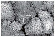
도 2 는, 실시예 1-1 에서 얻어진 PZT 계 강유전체 박막의 표면을 SEM (Scanning Electron Microscope, 주사형 전자 현미경) 으로 관찰했을 때의 사진이다.
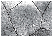
도 3 은, 비교예 1-2 에서 얻어진 PZT 계 강유전체 박막의 표면을 SEM 으로 관찰했을 때의 사진이다.
도 4 는, 본 발명 실시형태의 박막 형성시 고온 프로세스에 있어서의 온도 프로파일의 일례를 나타내는 그래프이다.1 is a cross-sectional schematic diagram of a PZT ferroelectric thin film according to an embodiment of the present invention.
Fig. 2 is a photograph of the surface of the PZT ferroelectric thin film obtained in Example 1-1 observed by SEM (Scanning Electron Microscope, scanning electron microscope). Fig.
Fig. 3 is a photograph of the surface of the PZT ferroelectric thin film obtained in Comparative Example 1-2 observed by SEM. Fig.
4 is a graph showing an example of a temperature profile in a high-temperature process when a thin film is formed according to an embodiment of the present invention.
다음으로 본 발명을 실시하기 위한 형태를 도면에 기초하여 설명한다.BEST MODE FOR CARRYING OUT THE INVENTION Next, embodiments for carrying out the present invention will be described with reference to the drawings.
본 실시형태의 PZT 계 강유전체 박막은, 도 1 에 나타내는 바와 같이, 하부 전극 (11) 을 갖는 기판의 그 하부 전극 (11) 상에 PZT 계 강유전체 박막 형성용 조성물을 1 회 또는 2 회 이상 도포하여 가소한 후, 소성하여 결정화시킴으로써 형성된 PZT 계 강유전체 박막 (21) 의 개량이다. 그 특징이 되는 구성은, 박막 (21) 표면에서 측정했을 때의 평균 입경이 500 ∼ 3000 ㎚ 의 범위에 있는 PZT 계 입자 (22) 로 박막 (21) 이 구성되고, 도포 1 회당 박막의 두께가 100 ∼ 400 ㎚ 의 범위가 되도록 형성한다는 점에서, PZT 결정 입자가 결정 성장한다는 이유에 의해, 또한 후술하는 바와 같이 종래보다 납량을 적게 하고 있다는 이유에 의해, 박막 (21) 표면에 있어서의 입계의 일부 또는 전부에 평균 입경이 20 ㎚ 이하인 상기 PZT 계 입자 (22) 와는 이질의 미립자 (23) 가 석출되어 있는 것에 있다.1, the PZT system ferroelectric thin film of the present embodiment is formed by applying a composition for forming a PZT system ferroelectric thin film one or more times onto the
본 실시형태의 PZT 계 강유전체 박막 (21) 은, 도포 1 회당 박막의 두께가 100 ∼ 400 ㎚ 의 범위가 되도록 형성된다. 100 ㎚ 미만에서는, PZT 결정 입자가 성장하지 않고, 박막 (21) 표면에 있어서의 입계의 일부 또는 전부에 상기 PZT 계 입자 (22) 와는 이질의 미립자 (23) 가 석출되지 않는다. 또한, 400 ㎚ 를 초과하면, 대량의 고분자 화합물을 필요로 하여 생산성이 떨어진다. 또한, 1 회의 도포로 형성되는 박막의 두께가 상한값을 초과하면 막이 다공성으로 됨으로써, 비유전율이 저하되고, 수명 특성도 저하되는 경향이 보인다. 한편, 하한값 미만에서는, 결정립이 잘아져 수명 신뢰성이 얻어지지 않는다. 또한, 생산성의 향상을 기대할 수 없기 때문에 바람직하지 못하다. 이와 같이, 본 실시형태의 PZT 계 강유전체 박막 (21) 은, 크랙의 발생이 적고, 나아가 1 회의 도포로 형성되는 박막의 두께가 수백 ㎚ 이기 때문에, 종래의 졸겔법에 의해 형성된 박막과 비교하여 생산 효율의 면 등에서 매우 우수하다. 이 중, 도포 1 회당 박막의 두께는 150 ∼ 300 ㎚ 의 범위에 있는 것이 특히 바람직하다. 또, 본 발명에 있어서, 도포 1 회당 박막의 두께란, 소성 후에 형성된 PZT 계 강유전체 박막의 총두께를 조성물의 도포 횟수로 나눈 두께를 말한다.The PZT ferroelectric
본 실시형태의 PZT 계 강유전체 박막 (21) 은, 박막 (21) 표면에서 측정했을 때의 평균 입경이 상기 범위에 있는 PZT 계 입자 (22) 로 구성됨으로써, 수명 특성을 향상시키는 효과가 얻어진다. PZT 계 강유전체 박막 (21) 은, 티탄산지르콘산납 (PZT) 등의 Pb 함유의 페로브스카이트 구조를 갖는 복합 금속 산화물로 구성되고, 상기 PZT 계 입자 (22) 란, 입계에 의해 격리된 하나의 결정립을 말한다. 박막 (21) 을 구성하는 PZT 계 입자 (22) 의 박막 표면에서 측정했을 때의 평균 입경을 상기 범위로 한정한 것은, 이 평균 입경이 하한값 미만에서는 수명 특성을 향상시키는 효과가 충분히 얻어지지 않고, 한편, 상한값을 초과하면 하나의 커패시터에 함유되는 입자수에 편차가 생겨, 소자의 특성의 편차가 커진다는 문제가 생기기 때문이다. 이 중, 상기 평균 입경은 1000 ∼ 2000 ㎚ 의 범위에 있는 것이 바람직하다. 입경 제어는 후술하는 조성물 중에 함유되는 고분자 화합물의 첨가량을 조정함으로써 사용할 수 있다. 또, 본 발명에 있어서, PZT 계 입자의 박막 표면에서 측정했을 때의 평균 입경이란, 박막 표면의 SEM 화상에 의해 관찰된 50 개의 PZT 계 입자의 입경을 평균한 값을 말한다. 이 때의 각 입자의 입경이란, 구형의 입자에 대해서는 그 직경을 말하고, 그 이외의 형상의 입자에 대해서는, 입자 중의 최장변과 이 최장변에 직각이면서 또한 최대인 변과의 평균값, 혹은, 입자 중의 최장경과 이 최장경에 직교하는 선분 중 최장 선분과의 평균값을 말한다.The PZT system ferroelectric
본 실시형태의 PZT 계 강유전체 박막 (21) 에는, PZT 외에, PZT 에 La 원소를 첨가한 PLZT 가 함유되고, Pb, Zr, Ti 등의 금속이 원하는 금속 원자비로 함유된다. 구체적으로는, Ti 및 Zr 의 합계 100 ㏖ 에 대하여 Pb 가 105 ∼ 115 ㏖ 이다. 즉, 예를 들어 일반식 : (PbxLay)(ZrzTi1 -z)O3 으로 나타냈을 때의 x 의 값이 1.05 ≤ x ≤ 1.15 의 범위를 취할 수 있다. 그리고, 본 실시형태의 PZT 계 강유전체 박막 (21) 에서는, Pb 의 비율을 상기 범위로 한정함으로써, 성장한 PZT 계 입자 (22) 의 입계에 결정립인 이질의 미립자 (23) (파이로클로르상 (相)) 을 석출시키고 있다.The PZT-system ferroelectric
즉, 본 실시형태의 PZT 계 강유전체 박막 (21) 은, 도 1 에 나타내는 바와 같이, 박막 (21) 표면에 있어서의 입계의 일부 또는 전부에 평균 입경이 20 ㎚ 이하인 상기 PZT 계 입자 (22) 와는 이질의 미립자 (23) 가 석출된 구조를 갖는다. 이 이질의 미립자 (23) 가 수명 특성을 향상시키는 역할을 하는 것으로 생각되고, 이것에 의해, 박막 (21) 이 갖는 전기 특성의 대폭적인 장수명화가 달성된다. 파이로클로르상은 원래 박막 안 등에 형성된 경우, 유전체 박막의 전기적 특성을 저하시키는 사실이 알려져 있지만, 본 실시형태에서는 파이로클로르상, 즉 이질의 미립자 (23) 을 박막 (21) 의 상기 특정 부위에 석출시키고, 또한 그 입경을 제어함으로써 박막 (21) 의 수명 특성을 향상시키고 있다. 또, 이질의 미립자 (23) 는, 박막 표면에 있어서, 전체 결정립계 중에 적어도 약 30 개 이상 존재하는 것이 바람직하다. 이것에 의해, 상기 서술한 효과를 충분히 얻을 수 있다.That is, as shown in Fig. 1, the PZT system ferroelectric
Pb 의 비율을 상기 범위로 한 것은, 상한값을 초과하면, 상기 이질의 미립자 (23) 가 입계에 석출되지 않아, 수명 특성의 향상 효과가 얻어지지 않기 때문이다. 한편, 하한값 미만에서는, 이질의 미립자 (23) 는 석출되지만, 비유전율이 낮아져, 커패시터로서의 기능 등을 저하시키기 때문이다. 이 중, Ti 및 Zr 의 합계 100 ㏖ 에 대하여 Pb 가 107 ∼ 110 ㏖ 함유되는 것이 바람직하다. 또, y 의 값은 0 ≤ y ≤ 0.1, z 의 값은 0.1 < z < 0.9 의 범위인 것이 바람직하다. 또한, 본 실시형태의 PZT 계 강유전체 박막 (21) 에는, PZT 외에, Mn 원소를 첨가한 PMnZT 나 Nb 원소를 첨가한 PNbZT 등도 함유된다. PZT 계 강유전체 박막 중의 이들 금속 원자비의 조정은, 박막 (21) 을 형성할 때에 사용되는 후술하는 조성물 중의 PZT 전구체의 배합비를 조정함으로써 실시할 수 있다.The reason why the ratio of Pb is set in the above range is that if the upper limit is exceeded, the
또한, 이질의 미립자 (23) 의 입경을 20 ㎚ 이하로 한정한 것은, 입경이 20 ㎚ 를 초과하면 리크 전류 밀도가 증대하는 문제가 생기기 때문이다. 이 중, 이질의 미립자 (23) 의 입경은 5 ∼ 15 ㎚ 의 범위인 것이 바람직하다. 이질의 미립자 (23) 의 성분은 주로 Pb2Ti2O7 인 파이로클로르상이고, 입경 제어는 상기 일반식에 있어서의 x 의 값을 변량 (變量) 함으로써 실시할 수 있다. 또한, 상기 특정 부위로의 석출은, 막 중의 유기 도펀트량을 조정함으로써 실시할 수 있다. 또, 본 발명에 있어서, 이질의 미립자의 입경이란, 박막 표면의 SEM 화상에 의해 관찰된 50 개의 이질의 미립자의 입경을 평균한 값을 말한다. 이 때의 각 입자의 입경이란, 입자 중의 최장변과 이 최장변에 직각이면서 또한 최소인 변과의 평균값, 혹은, 입자 중의 최장경과 이 최장경에 직교하는 선분 중 최단 선분과의 평균값을 말한다.The reason why the particle diameter of the
또한, 박막 (21) 의 총두께는 100 ∼ 5000 ㎚ 의 범위에 있는 것이 바람직하다. 총두께가 100 ㎚ 미만에서는 생산성이 나쁜 막이 되고, 또한, 리크 전류 밀도가 높아지는 등의 특성면에서의 문제가 발생하는 경우가 있다. 한편, 상한값을 초과하면 크랙이 발생하기 쉬운 경향이 있다. 이 중, 총두께는 300 ∼ 3000 ㎚ 의 범위에 있는 것이 특히 바람직하다.The total thickness of the
계속해서, 본 실시형태의 PZT 계 강유전체 박막의 형성 방법에 관해서 설명한다. 먼저, 하부 전극을 갖는 기판의 그 하부 전극 상에 PZT 계 강유전체 박막 형성용 조성물을 1 회 또는 2 회 이상 도포하여, 원하는 두께를 갖는 도막 (겔막) 을 형성한다. 이 때의 조성물의 1 회당 도포량은, 전술한 바와 같이, 도포 1 회당 박막의 두께가 100 ∼ 400 ㎚ 의 범위가 되도록 설정하는 것이 바람직하다. 도포법에 대해서는 특별히 한정되지 않지만, 스핀 코트, 딥 코트, LSMCD (Liquid Source Misted Chemica1 Deposition) 법 또는 스핀 스프레이법 등을 들 수 있다. 강유전체 박막을 형성하는 기판은, 그 용도 등에 따라서도 달라지지만, 예를 들어 박막 커패시터 등의 유전체층을 형성하는 경우, 하부 전극이 형성된 실리콘 기판이나 사파이어 기판 등의 내열성 기판이 사용된다. 기판 상에 형성하는 하부 전극으로는, Pt 나 Ir, Ru 등의 도전성을 갖고, 강유전체 박막과 반응하지 않는 재료가 사용된다. 또한, 기판 상에 밀착층이나 절연체막 등을 개재하여 하부 전극을 형성한 기판 등을 사용할 수도 있다. 구체적으로는, Pt/Ti/SiO2/Si, Pt/TiO2/SiO2/Si, Pt/IrO/Ir/SiO2/Si, Pt/TiN/SiO2/Si, Pt/Ta/SiO2/Si, Pt/Ir/SiO2/Si 의 적층 구조 (하부 전극/밀착층/절연체막/기판) 를 갖는 기판 등을 들 수 있다. 또한, 압전 소자나 초전형 적외선 검출 소자 등에서는, 실리콘 기판, SiO2/Si 기판, 사파이어 기판 등의 내열성 기판을 사용할 수 있다.Next, a method of forming the PZT ferroelectric thin film of the present embodiment will be described. First, a coating film (gel film) having a desired thickness is formed by applying a composition for forming a PZT ferroelectric thin film on the lower electrode of the substrate having the lower electrode once or twice or more. It is preferable that the coating amount per one time of the composition at this time is set so that the thickness of the thin film per application is in the range of 100 to 400 nm as described above. The coating method is not particularly limited, but spin coating, dip coating, LSMCD (Liquid Source Misted Chemistry Deposition) method, spin spray method and the like can be mentioned. The substrate on which the ferroelectric thin film is formed differs depending on its use. For example, when a dielectric layer such as a thin film capacitor is formed, a heat-resistant substrate such as a silicon substrate or a sapphire substrate on which a lower electrode is formed is used. As the lower electrode to be formed on the substrate, a material having conductivity such as Pt, Ir, or Ru and not reacting with the ferroelectric thin film is used. It is also possible to use a substrate having a lower electrode formed on a substrate with an adhesive layer or an insulating film interposed therebetween. Specifically, Pt / Ti / SiO 2 / Si, Pt / TiO 2 / SiO 2 / Si, Pt / IrO / Ir / SiO 2 / Si, Pt / TiN / SiO 2 / Si, Pt / Ta / SiO 2 / Si, and a substrate having a laminated structure of Pt / Ir / SiO 2 / Si (lower electrode / adhesion layer / insulator film / substrate). Further, in the piezoelectric element, the superconducting infrared detecting element, etc., a heat-resistant substrate such as a silicon substrate, a SiO 2 / Si substrate, or a sapphire substrate can be used.
PZT 계 강유전체 박막 형성용 조성물은, PZT 계 강유전체 박막을 형성하기 위한 원료 용액으로, 형성 후의 강유전체 박막에 있어서 상기 서술한 복합 금속 산화물 등을 구성하기 위한 원료 (PZT 전구체) 를 원하는 비율로 적당한 용매에 용해하여, 도포에 적합한 농도로 조정한 유기 금속 화합물 용액으로 이루어진다.The composition for forming a PZT system ferroelectric thin film is a raw material solution for forming a PZT system ferroelectric thin film, and a raw material (PZT precursor) for constituting the above-described complex metal oxide or the like in the formed ferroelectric thin film is dissolved in a suitable solvent And is dissolved and adjusted to a concentration suitable for application.
PZT 전구체는, Pb, La, Zr 또는 Ti 등의 각 금속 원소에, 유기기가 그 산소 또는 질소 원자를 사이에 두고 결합하고 있는 화합물이 바람직하다. 예를 들어, 금속 알콕사이드, 금속 디올 착물, 금속 트리올 착물, 금속 카르복실산염, 금속 β-디케토네이트 착물, 금속 β-디케토에스테르 착물, 금속 β-이미노케토 착물, 및 금속 아미노 착물로 이루어지는 군에서 선택된 1 종 또는 2 종 이상이 예시된다. 특히 바람직한 화합물은, 금속 알콕사이드, 그 부분 가수분해물, 유기산염이다.The PZT precursor is preferably a compound in which an organic group binds to each metal element such as Pb, La, Zr or Ti with the oxygen or nitrogen atom interposed therebetween. For example, metal complexes such as metal alkoxide, metal diol complex, metal triol complex, metal carboxylate, metal? -Diketonate complex, metal? -Diketo ester complex, metal? -Iminocate complex, And one or more selected from the group consisting of Particularly preferred compounds are metal alkoxides, partial hydrolyzates thereof, and organic acid salts.
구체적으로, Pb 화합물, La 화합물로는, 아세트산납 : Pb(OAc)2, 아세트산란탄 : La(OAc)3 등의 아세트산염이나, 납디이소프로폭사이드 : Pb(OiPr)2, 란탄트리이소프로폭사이드 : La(OiPr)3 등의 알콕사이드를 들 수 있다. Ti 화합물로는, 티탄테트라에톡사이드 : Ti(OEt)4, 티탄테트라이소프로폭사이드 : Ti(OiPr)4, 티탄테트라 n-부톡사이드 : Ti(OiBu)4, 티탄테트라이소부톡사이드 : Ti(OiBu)4, 티탄테트라 t-부톡사이드 : Ti(OtBu)4, 티탄디메톡시디이소프로폭사이드 : Ti(OMe)2(OiPr)2 등의 알콕사이드를 들 수 있다. Zr 화합물로는, 상기 Ti 화합물과 동일한 알콕사이드류가 바람직하다. 금속 알콕사이드는 그대로 사용해도 되지만, 분해를 촉진시키기 위해 그 부분 가수분해물을 사용해도 된다. 또, Mn 화합물로는, 2-에틸헥산산망간, 나프텐산망간 또는 아세트산망간 등을 들 수 있다. 또한, Nb 화합물로는, 2-에틸헥산산니오븀 또는 니오븀펜타에톡사이드 등을 들 수 있다.Specifically, examples of the Pb compound and La compound include acetic acid salts such as lead acetate: Pb (OAc) 2 and lanthanum acetate: La (OAc) 3 , and lead acetate such as lead diisopropoxide: Pb (OiPr) 2 , And an alkoxide such as a lateral side: La (OiPr) 3 . Examples of the Ti compound include titanium tetraethoxide: Ti (OEt) 4 , titanium tetraisopropoxide: Ti (OiPr) 4 , titanium tetra n-butoxide: Ti (OiBu) 4 , titanium tetraisobutoxide: Ti (OiBu) 4 , titanium tetra-t-butoxide: Ti (OtBu) 4 and titanium dimethoxydiisopropoxide: Ti (OMe) 2 (OiPr) 2 . The Zr compound is preferably the same alkoxide as the Ti compound. The metal alkoxide may be used as it is, but the partial hydrolyzate may be used to promote decomposition. Examples of the Mn compound include manganese 2-ethylhexanoate, manganese naphthenate, and manganese acetate. Examples of the Nb compound include niobium 2-ethylhexanoate or niobium pentaethoxide.
PZT 계 강유전체 박막 형성용 조성물에는, 조성물을 조제할 때에 이들의 비율을 조정함으로써 상기 서술한 원하는 금속 원자비를 제공하는 비율로, Ti, Zr, Pb 가 함유된다. 즉, 조성물에는, Ti 및 Zr 의 합계 100 ㏖ 에 대하여 Pb 가 105 ∼ 115 ㏖, 바람직하게는 107 ∼ 110 ㏖ 함유된다. 조성물 중의 Pb 의 비율이 상기 범위에서 벗어나면, 형성 후의 박막 중에 있어서의 Pb 의 비율도 상기 서술한 범위에서 벗어나, 상기 서술한 문제가 생기기 때문이다.The composition for forming a PZT-based ferroelectric thin film contains Ti, Zr, and Pb at a ratio to provide the above-described desired metal atomic ratio by adjusting the ratio thereof when preparing the composition. That is, the composition contains Pb in an amount of 105 to 115 moles, preferably 107 to 110 moles per 100 moles in total of Ti and Zr. If the ratio of Pb in the composition deviates from the above range, the ratio of Pb in the thin film after formation also deviates from the above-described range, resulting in the above-described problem.
조성물 100 질량% 중에서 차지하는 상기 PZT 전구체의 비율은 산화물 환산으로 15 ∼ 35 질량% 로 하는 것이 바람직하다. PZT 전구체의 비율을 상기 범위로 한 것은, 하한값 미만에서는 1 회의 도포로 충분한 막두께가 얻어지기 어렵고, 한편, 상한값을 초과하면 크랙이 발생하기 쉬운 경향이 있기 때문이다. 또, 산화물 환산에 의한 비율이란, 조성물에 함유되는 금속 원소가 모두 산화물이 되었다고 가정했을 때에, 조성물 100 질량% 에서 차지하는 금속 산화물의 비율을 말한다.The proportion of the PZT precursor in 100 mass% of the composition is preferably 15 to 35 mass% in terms of oxide. If the ratio of the PZT precursor is within the above range, a film thickness less than a lower limit value is not enough to be obtained by one application, while cracks tend to occur when the upper limit value is exceeded. The ratio by oxide conversion refers to the ratio of the metal oxide occupying 100% by mass of the composition, assuming that all the metal elements contained in the composition are oxides.
조성물의 조제에 사용되는 용매는 사용하는 원료에 따라서 적절히 결정되지만, 일반적으로는, 카르복실산, 알코올 (예를 들어, 에탄올이나 1-부탄올, 다가 알코올인 프로필렌글리콜, 에틸렌글리콜 등), 에스테르, 케톤류 (예를 들어, 아세톤, 메틸에틸케톤), 에테르류 (예를 들어, 디메틸에테르, 디에틸에테르), 시클로알칸류 (예를 들어, 시클로헥산, 시클로헥산올), 방향족계 (예를 들어, 벤젠, 톨루엔, 자일렌), 기타 테트라하이드로푸란 등, 또는 이들의 2 종 이상의 혼합 용매를 사용할 수 있다.The solvent used in the preparation of the composition is appropriately determined depending on the raw material to be used and is generally selected from the group consisting of carboxylic acids, alcohols (e.g., ethanol or 1-butanol, polyhydric alcohols such as propylene glycol and ethylene glycol) (For example, acetone, methyl ethyl ketone), ethers (e.g., dimethyl ether, diethyl ether), cycloalkanes (e.g., cyclohexane, cyclohexanol) , Benzene, toluene, xylene), other tetrahydrofuran, or a mixture of two or more of these solvents.
카르복실산으로는, 구체적으로는, n-부티르산, α-메틸부티르산, i-발레르산, 2-에틸부티르산, 2,2-디메틸부티르산, 3,3-디메틸부티르산, 2,3-디메틸부티르산, 3-메틸펜탄산, 4-메틸펜탄산, 2-에틸펜탄산, 3-에틸펜탄산, 2,2-디메틸펜탄산, 3,3-디메틸펜탄산, 2,3-디메틸펜탄산, 2-에틸헥산산, 3-에틸헥산산을 사용하는 것이 바람직하다. Specific examples of the carboxylic acid include n-butyric acid, alpha -methylbutyric acid, i-valeric acid, 2-ethylbutyric acid, 2,2-dimethylbutyric acid, 3,3-dimethylbutyric acid, 3-methylpentanoic acid, 2-ethylpentanoic acid, 3-ethylpentanoic acid, 2,2-dimethylpentanoic acid, 3,3-dimethylpentanoic acid, 2,3- Ethylhexanoic acid, and 3-ethylhexanoic acid are preferably used.
또한 에스테르로는, 아세트산에틸, 아세트산프로필, 아세트산 n-부틸, 아세트산 sec-부틸, 아세트산 tert-부틸, 아세트산이소부틸, 아세트산 n-아밀, 아세트산 sec-아밀, 아세트산 tert-아밀, 아세트산이소아밀을 사용하는 것이 바람직하고, 알코올로는, 1-프로판올, 2-프로판올, 1-부탄올, 2-부탄올, 이소-부틸알코올, 1-펜탄올, 2-펜탄올, 2-메틸-2-펜탄올, 2-메톡시에탄올을 사용하는 것이 바람직하다.Examples of esters include ethyl acetate, propyl acetate, n-butyl acetate, sec-butyl acetate, tert-butyl acetate, isobutyl acetate, n-amyl acetate, sec-amyl acetate, And examples of the alcohol include alcohols such as 1-propanol, 2-propanol, 1-butanol, 2-butanol, iso-butyl alcohol, It is preferable to use 2-methoxyethanol.
또한, 상기 조성물에는, 폴리비닐피롤리돈 (PVP) 또는 폴리에틸렌글리콜 등의 고분자 화합물을 함유시킨다. 폴리비닐피롤리돈 및 폴리에틸렌글리콜은, 예를 들어 조성물 중의 액 점도를 조정하기 위해서 함유된다. 폴리비닐피롤리돈은, k 값에 의해 상대 점도를 결정하여 조제할 수 있다. 여기서 k 값이란, 분자량과 상관하는 점성 특성치로, 모세관 점도계에 의해 측정되는 상대 점도값 (25 ℃) 을 하기 Fikentscher 의 식에 적용하여 산출되는 값이다.Further, a polymer compound such as polyvinyl pyrrolidone (PVP) or polyethylene glycol is contained in the composition. Polyvinyl pyrrolidone and polyethylene glycol are contained, for example, in order to adjust the liquid viscosity in the composition. Polyvinylpyrrolidone can be prepared by determining the relative viscosity by k value. Here, the k value is a value calculated by applying the relative viscosity value (25 캜) measured by the capillary viscometer to the formula of Fikentscher, which is a viscosity characteristic value correlated with the molecular weight.
k 값 = (1.5logηrel-1)/(0.15+0.003c) k value = (1.5log? rel-1) / (0.15 + 0.003c)
+(300clogηrel+(c+1.5clogηrel)2)1/2/(0.15c+0.003c2)+ (300 clog? Er + (c + 1.5 clog? Rel) 2 ) 1/2 / (0.15 c + 0.003 c 2 )
상기 식 중, 「ηrel」은, 폴리비닐피롤리돈 수용액의 물에 대한 상대 점도를 나타내고, 「c」는, 폴리비닐피롤리돈 수용액 중의 폴리비닐피롤리돈 농도 (wt%) 를 나타낸다.Represents the relative viscosity of the polyvinyl pyrrolidone aqueous solution to water, and " c " represents the polyvinyl pyrrolidone concentration (wt%) in the polyvinyl pyrrolidone aqueous solution.
조성물에 함유되는 폴리비닐피롤리돈의 k 값은 15 ∼ 90 인 것이 바람직하다. 두께가 있는 강유전체 박막을 형성하기 위해서는, 조성물을 기판 등에 도포할 때, 도포된 도막 (겔막) 이 그 두께를 유지하기 위해서 충분한 점도가 필요한데, k 값이 하한값 미만에서는, 그것을 얻기 어렵다. 한편, 상한값을 초과하면 점도가 지나치게 높아져, 조성물을 균일하게 도포하기가 곤란해진다. 또한, 폴리에틸렌글리콜을 사용하는 경우에는, 중합도가 200 ∼ 1000 인 것을 사용하는 것이 바람직하다. 중합도가 하한값 미만에서는 상기 점도를 충분히 얻기 힘들고, 한편, 중합도가 상한값을 초과하면 점도가 지나치게 높아져, 조성물을 균일하게 도포하기가 곤란해지기 때문이다. 또한, 폴리비닐피롤리돈은, 크랙 억제 효과가 크기 때문에 특히 바람직하다.The k value of the polyvinylpyrrolidone contained in the composition is preferably from 15 to 90. In order to form a thick ferroelectric thin film, when the composition is applied to a substrate or the like, a sufficient viscosity is required to maintain the applied coating film (gel film) in its thickness, but when the k value is less than the lower limit value, it is difficult to obtain. On the other hand, when the upper limit is exceeded, the viscosity becomes excessively high, making it difficult to apply the composition uniformly. When polyethylene glycol is used, it is preferable to use polyethylene glycol having a degree of polymerization of 200 to 1000. If the polymerization degree is below the lower limit value, it is difficult to sufficiently obtain the viscosity. On the other hand, if the degree of polymerization exceeds the upper limit value, the viscosity becomes too high, and it becomes difficult to uniformly coat the composition. Polyvinyl pyrrolidone is particularly preferable because it has a large crack suppressing effect.
폴리비닐피롤리돈 또는 폴리에틸렌글리콜 등의 고분자 화합물의 비율은, 상기 PZT 전구체 1 몰에 대하여 모노머 환산으로 0.15 ∼ 0.50 몰의 범위로 한다. 하한값 미만에서는, 크랙이 발생하기 쉬운 경향이 있고, 한편, 상한값을 초과하면 포어가 생기기 쉬운 경향이 있다. 또한, 고분자 화합물의 비율이 이 범위에서 벗어나면, PZT 계 입자의 평균 입경이 상기 원하는 범위에서 벗어남으로써, 상기 서술한 문제가 생기는 경향이 보인다.The proportion of the polymer compound such as polyvinylpyrrolidone or polyethylene glycol is in the range of 0.15 to 0.50 moles in terms of monomer relative to 1 mole of the PZT precursor. Below the lower limit value, cracks tend to occur. On the other hand, when the upper limit value is exceeded, pores tend to occur easily. When the ratio of the polymer compound is out of this range, the above-mentioned problem tends to occur when the average particle diameter of the PZT-based particles deviates from the above-mentioned desired range.
또, 여기서 모노머 환산에 의한 몰값이란, 고분자를 구성하는 모노머의 분자량을 기준으로 한 몰값을 의미하고, PZT 전구체 1 몰에 대한 모노머 환산의 몰값이란, 고분자를 구성하는 모노머의 분자량을 기준으로 한 PZT 전구체 1 몰에 대한 몰값을 의미한다.Here, the molar value in terms of the monomer means a molar value based on the molecular weight of the monomer constituting the polymer, and the molar value in terms of the monomer with respect to 1 mol of the PZT precursor is a molar value based on the molecular weight of the monomer constituting the polymer, Means the molar value with respect to one mole of the precursor.
또한, 상기 성분 이외에, 필요에 따라서 안정화제로서, β-디케톤류 (예를 들어, 아세틸아세톤, 헵타플루오로부타노일피발로일메탄, 디피발로일메탄, 트리플루오로아세틸아세톤, 벤조일아세톤 등), β-케톤산류 (예를 들어, 아세토아세트산, 프로피오닐아세트산, 벤조일아세트산 등), β-케토에스테르류 (예를 들어, 상기 케톤산의 메틸, 프로필, 부틸 등의 저급 알킬에스테르류), 옥시산류 (예를 들어, 락트산, 글리콜산, α-옥시부티르산, 살리실산 등), 상기 옥시산의 저급 알킬에스테르류, 옥시케톤류 (예를 들어, 디아세톤알코올, 아세토인 등), 디올, 트리올, 고급 카르복실산, 알칸올아민류 (예를 들어, 디에탄올아민, 트리에탄올아민, 모노에탄올아민), 다가 아민 등을, (안정화제 분자수)/(금속 원자수) 로 0.2 ∼ 3 정도 첨가해도 된다.Further, in addition to the above components, β-diketones (for example, acetyl acetone, heptafluorobutanoyl pivaloyl methane, dipivaloyl methane, trifluoroacetylacetone, benzoyl acetone, etc.) (for example, lower alkyl esters such as methyl, propyl, butyl and the like of the above-mentioned ketonic acid), oxo (meth) acrylates (For example, diacetone alcohol, acetone and the like), diols, triols, triols, and the like, as well as organic acids (for example, lactic acid, glycolic acid,? -Oxybutyric acid, salicylic acid, (Stabilizer molecule number) / (number of metal atoms) may be added in an amount of from about 0.2 to about 3, for example, in the presence of a base such as an alkali metal carbonate, an alkali metal carbonate, an alkali metal carbonate,
상기 조성물은 β-디케톤류 및 다가 알코올류를 함유하고 있는 것이 바람직하다. 이 중, β-디케톤류로는 아세틸아세톤이, 다가 알코올류로는 프로필렌글리콜이 특히 바람직하다.It is preferable that the composition contains? -Diketones and polyhydric alcohols. Of these, acetylacetone is preferable as the? -Diketones, and propylene glycol is particularly preferable as the polyhydric alcohols.
또한 상기 조성물에는, 포름아미드계 용제 등의 극성 용매를, 유기 도펀트로서 함유시키는 것이 바람직하다. 포름아미드계 용제에는, 포름아미드, N-메틸포름아미드 또는 N,N-디메틸포름아미드 중 어느 것을 사용하는 것이 바람직하다. 상기 폴리비닐피롤리돈 등과의 조합에 의해, 더욱 크랙이 적고, 또한 치밀한 막 구조를 갖는 막을 형성할 수 있다. 또한, 조성물을 도포할 때에 보다 균일한 도막을 형성할 수 있으며, 나아가, 소성시에 있어서의 용매의 탈락을 양호하게 하는 효과가 보다 높아진다. 상기 포름아미드계 용제 이외의 유기 도펀트로는, 모노에탄올아민이나 디에탄올아민 등의 에탄올아민류를 들 수 있고, 상기 포름아미드계 용제와의 병용도 가능하다. 이들은, 금속 알콕사이드에 배위되어 용액의 보존 안정성을 높이는 효과가 있기 때문에 바람직하다. 포름아미드계 용제를 함유하는 유기 도펀트의 비율은, 조성물 100 질량% 중 3 ∼ 15 질량% 의 비율로 하는 것이 바람직하다.In addition, it is preferable that a polar solvent such as a formamide solvent is contained in the composition as an organic dopant. As the formamide-based solvent, it is preferable to use any of formamide, N-methylformamide or N, N-dimethylformamide. By combining with polyvinyl pyrrolidone and the like, a film having a smaller crack and a dense film structure can be formed. Further, a more uniform coating film can be formed when the composition is applied, and further, the effect of satisfactorily removing the solvent at the time of firing is further enhanced. Examples of organic dopants other than the above-mentioned formamide solvents include ethanol amines such as monoethanolamine and diethanolamine, and it is also possible to use them in combination with the above-mentioned formamide solvents. These are preferable because they have an effect of coordinating with the metal alkoxide to enhance the storage stability of the solution. The proportion of the organic dopant containing a formamide-based solvent is preferably 3 to 15% by mass in 100% by mass of the composition.
상기 조성물을 조제하기 위해서는, 먼저, 상기 서술한 Pb 화합물 등의 PZT 전구체를 각각 준비하고, 이들을 상기 원하는 금속 원자비를 제공하는 비율이 되도록 칭량한다. 칭량한 상기 PZT 전구체와 프로필렌글리콜 등의 용매를 반응 용기 내에 투입하여 혼합하고, 바람직하게는 질소 분위기 중, 150 ∼ 160 ℃ 의 온도에서 0.5 ∼ 3 시간 환류하여 반응시킴으로써 합성액을 조제한다. 환류 후에는, 증류나 이배퍼레이션 등의 방법에 의해 탈용매시켜 두는 것이 바람직하다. 또한, 아세틸아세톤 등의 안정화제를 첨가하는 경우에는, 탈용매 후의 합성액에 이들을 첨가하고, 질소 분위기 중, 150 ∼ 160 ℃ 의 온도에서 0.5 ∼ 3 시간 환류를 실시하는 것이 바람직하다.In order to prepare the above composition, first, PZT precursors such as the above-mentioned Pb compound are prepared, and these are weighed so as to provide the desired metal atomic ratio. The weighed PZT precursor and a solvent such as propylene glycol are put into a reaction vessel and mixed, and the reaction mixture is reacted by refluxing at a temperature of 150 to 160 ° C in a nitrogen atmosphere for 0.5 to 3 hours to prepare a synthesis solution. After the reflux, desolvation is preferably performed by a method such as distillation or divalation. When a stabilizer such as acetylacetone is added, it is preferable to add them to the synthesis solution after desolvation and reflux at a temperature of 150 to 160 캜 for 0.5 to 3 hours in a nitrogen atmosphere.
그 후, 다시 용매를 첨가, 혼합함으로써 농도 조정을 실시한 후, 포름아미드계 용제를 함유하는 유기 도펀트를 첨가하고, 추가로 알코올 등의 다른 용매를 첨가, 교반하여 희석시킴으로써, 조성물 중에서 차지하는 각 성분 농도를 상기 서술한 원하는 농도로 조정한다. 여기에, 폴리비닐피롤리돈 등의 고분자 화합물을 원하는 비율이 되도록 첨가하고, 바람직하게는 실온에서 0.5 ∼ 3 시간 교반함으로써 균일하게 분산시킨다. 이것에 의해, 본 실시형태의 PZT 계 강유전체 박막 형성용 조성물이 얻어진다.Thereafter, the concentration is adjusted by addition and mixing of the solvent again, and then an organic dopant containing a formamide-based solvent is added. Further, another solvent such as alcohol is added and the mixture is stirred to dilute each component Is adjusted to the above-described desired concentration. A polymer compound such as polyvinylpyrrolidone is added thereto in a desired ratio, and the mixture is uniformly dispersed by stirring at room temperature for 0.5 to 3 hours. Thus, the composition for forming a PZT-based ferroelectric thin film of the present embodiment is obtained.
또, 조성물의 조제 후, 여과 처리 등에 의해 파티클을 제거하여, 입경 0.5 ㎛ 이상 (특히 0.3 ㎛ 이상 그 중에서도 0.2 ㎛ 이상) 인 파티클의 개수가 조성물 1 ㎖ 당 50 개/㎖ 이하로 하는 것이 바람직하다. 조성물 중의 입경 0.5 ㎛ 이상인 파티클의 개수가 50 개/㎖ 를 초과하면, 장기 보존 안정성이 떨어지는 것이 된다. 이 조성물 중의 입경 0.5 ㎛ 이상인 파티클의 개수는 적을수록 바람직하고, 특히 30 개/㎖ 이하인 것이 바람직하다.Further, it is preferable that the number of particles having a particle diameter of 0.5 占 퐉 or more (particularly 0.3 占 퐉 or more and 0.2 占 퐉 or more in particular) is removed to 50 / ml or less per 1 ml of the composition by removing the particles by filtration or the like after preparation of the composition . If the number of particles having a particle diameter of 0.5 占 퐉 or more in the composition exceeds 50 / ml, the long-term storage stability becomes poor. The number of particles having a particle diameter of 0.5 m or more in this composition is preferably as small as possible, particularly preferably 30 particles / ml or less.
상기 파티클 개수가 되도록, 조제 후의 조성물을 처리하는 방법은 특별히 한정되는 것은 아니지만, 예를 들어, 다음과 같은 방법을 들 수 있다. 제 1 방법으로는, 시판되는 0.2 ㎛ 공경 (孔徑) 의 멤브레인 필터를 사용하여, 시린지로 압송하는 여과법이다. 제 2 방법으로는, 시판되는 0.05 ㎛ 공경의 멤브레인 필터와 가압 탱크를 조합한 가압 여과법이다. 제 3 방법으로는, 상기 제 2 방법에서 사용한 필터와 용액 순환조를 조합한 순환 여과법이다.The method of treating the composition after the preparation so as to have the above-mentioned number of particles is not particularly limited. For example, the following methods can be mentioned. The first method is a filtration method in which a commercially available membrane filter having a pore size of 0.2 탆 is used and pressure-fed by a syringe. The second method is a pressurized filtration method in which a commercially available membrane filter having a pore size of 0.05 mu m and a pressurizing tank are combined. The third method is a circulation filtration method in which the filter used in the second method and the solution circulation tank are combined.
어느 방법에 있어서도, 조성물의 압송 압력에 따라, 필터에 의한 파티클 포착률이 상이하다. 압력이 낮을수록 포착률이 높아지는 것이 일반적으로 알려져 있으며, 특히, 제 1 방법, 제 2 방법에서, 입경 0.5 ㎛ 이상인 파티클의 개수를 50 개 이하로 하는 조건을 실현하기 위해서는, 조성물을 저압으로 매우 천천히 필터에 통과시키는 것이 바람직하다.In any of the methods, the particle capture ratio by the filter is different depending on the pressure of the composition to be fed. It is generally known that the lower the pressure is, the higher the trapping rate. Particularly, in the first method and the second method, in order to realize a condition that the number of particles having a particle diameter of 0.5 탆 or more is 50 or less, .
이렇게 해서 얻어진 조성물을 하부 전극 상에 도포하여, 도막을 형성한 후에는, 이 도막을 가소하고, 다시 소성함으로써 결정화시킨다. 가소는, 핫 플레이트 또는 RTA 등을 사용하여, 대기 분위기 중, 150 ∼ 450 ℃, 1 ∼ 10 분간 실시하는 것이 바람직하다. 실온에서부터 가소 온도까지의 승온 속도는 2.5 ∼ 50 ℃/초로 하는 것이 바람직하다. 가소는, 용매를 제거하는 것과 함께 금속 화합물을 열분해 또는 가수분해하여 복합 산화물로 전화시키기 위해서 실시한다는 점에서, 공기 중, 산화 분위기 중, 또는 함수 증기 분위기 중에서 실시하는 것이 바람직하다. 공기 중에서의 가열이라도, 가수분해에 필요한 수분은 공기 중의 습기에 의해 충분히 확보된다. 이 가열은, 용매의 제거를 위한 저온 가열과, 유기 금속 화합물의 분해를 위한 고온 가열의 2 단계로 실시해도 된다.After the thus obtained composition is applied on the lower electrode and the coating film is formed, the coating film is calcined and then fired to crystallize it. The preliminary firing is preferably carried out at 150 to 450 DEG C for 1 to 10 minutes in an atmospheric environment using a hot plate, RTA or the like. The rate of temperature rise from room temperature to the calcining temperature is preferably 2.5 to 50 DEG C / sec. The firing is preferably carried out in air, in an oxidizing atmosphere, or in a steam atmosphere in that the firing is carried out in order to remove the solvent and to pyrolyze or hydrolyze the metal compound to convert it into a composite oxide. Even in heating in air, moisture required for hydrolysis is sufficiently secured by moisture in the air. This heating may be performed in two steps of low-temperature heating for removing the solvent and high-temperature heating for decomposing the organic metal compound.
또, 도포에서 가소까지의 공정은 각각 1 회로 실시해도 되지만, 원하는 막두께가 되도록 가소까지의 공정을 복수 회 반복하고, 마지막으로 일괄적으로 소성을 실시하는 것이 바람직하다.The steps from the application to the firing may be performed once, respectively. However, it is preferable that the steps up to the firing are repeated a plurality of times so as to obtain a desired film thickness, and finally, the firing is performed all at once.
소성은, 가소 후의 도막을 결정화 온도 이상의 온도에서 소성하여 결정화시키기 위한 공정으로, 이것에 의해 강유전체 박막이 얻어진다. 이 결정화 공정의 소성 분위기는 O2, N2, Ar, N2O 또는 H2 등 또는 이들의 혼합 가스 등이 바람직하다. 소성은, 600 ∼ 700 ℃ 에서 1 ∼ 5 분간 정도 실시된다. 소성은, 급속 가열 처리 (RTA 처리) 로 실시해도 된다. RTA 처리로 소성하는 경우, 그 승온 속도를 2.5 ∼ 100 ℃/초로 하는 것이 바람직하다.The firing is a step for firing the coated film after calcination at a temperature equal to or higher than the crystallization temperature, thereby obtaining a ferroelectric thin film. The firing atmosphere in this crystallization step is preferably O 2 , N 2 , Ar, N 2 O, H 2 , or a mixed gas thereof. The firing is carried out at 600 to 700 ° C for about 1 to 5 minutes. The firing may be performed by rapid heating treatment (RTA treatment). In the case of firing by RTA treatment, it is preferable to set the heating rate to 2.5 to 100 ° C / second.
이상의 공정에 의해, PZT 계 강유전체 박막이 얻어진다. 이 형성 방법에서는, 도포 등의 성막시 공정수가 적고, 비교적 간편하게 두꺼운 막을 형성할 수 있음에도 불구하고, 얻어진 막은 크랙이 매우 적다. 또한, 치밀한 막 구조를 갖기 때문에, 전기 특성이 매우 우수하고, 나아가 대폭적인 장수명화를 도모할 수 있다.By the above process, a PZT ferroelectric thin film can be obtained. In this forming method, although the number of steps for film formation such as application is small and a relatively thick film can be formed relatively easily, the obtained film has very few cracks. In addition, since it has a dense film structure, its electrical characteristics are excellent, and it is possible to achieve remarkable long life.
이 때문에, 본 실시형태의 방법에 의해서 얻어진 PZT 계 강유전체 박막은, 박막 콘덴서, 커패시터, IPD, DRAM 메모리용 콘덴서, 적층 콘덴서, 트랜지스터의 게이트 절연체, 불휘발성 메모리, 초전형 적외선 검출 소자, 압전 소자, 전기 광학 소자, 액추에이터, 공진자, 초음파 모터, 전기 스위치, 광학 스위치 또는 LC 노이즈 필터 소자의 복합 전자 부품을 제조할 때의 구성 재료로서 바람직하게 사용할 수 있다.Therefore, the PZT ferroelectric thin film obtained by the method of this embodiment can be used as a thin film capacitor, a capacitor, an IPD, a capacitor for a DRAM memory, a laminated capacitor, a gate insulator of a transistor, a nonvolatile memory, It can be preferably used as a constituent material in manufacturing a composite electronic component of an electrooptical element, an actuator, a resonator, an ultrasonic motor, an electric switch, an optical switch or an LC noise filter element.
실시예Example
다음으로 본 발명의 실시예를 비교예와 함께 자세히 설명한다.Next, examples of the present invention will be described in detail with reference to comparative examples.
<실시예 1-1> ≪ Example 1-1 >
먼저, 금속 원자비가 115/52/48 (Pb/Zr/Ti) 가 되도록, PZT 전구체로서 아세트산납삼수화물 (Pb 원 (源)), 테트라티타늄이소프로폭사이드 (Ti 원), 테트라지르코늄부톡사이드 (Zr 원) 를 각각 칭량하고, 이들을 반응 용기 내의 프로필렌글리콜에 첨가하여 합성액을 조제하였다. 이 합성액을 질소 분위기 중, 150 ℃ 의 온도에서 60 분간 환류한 후, 증류에 의해 탈용매하였다. 그 후, 안정화제로서 아세틸아세톤을 첨가하였다.First, lead trihydrate (Pb source), tetra-titanium isopropoxide (Ti source), tetrazirconium butoxide (Pb source) as a PZT precursor were mixed so that the metal atomic ratio became 115/52/48 (Pb / Zr / Ti) (Zr source) were respectively weighed and added to propylene glycol in a reaction vessel to prepare a synthesis solution. This synthesis solution was refluxed in a nitrogen atmosphere at a temperature of 150 캜 for 60 minutes and then desolvated by distillation. Thereafter, acetylacetone was added as a stabilizer.
이어서, 상기 합성액에 프로필렌글리콜을 첨가함으로써, PZT 전구체의 농도가 산화물 환산으로 35 질량% 가 될 때까지 희석하였다. 또, 에탄올과 N-메틸포름아미드를 첨가하여, PZT 전구체의 농도가 산화물 환산으로 25 질량% 까지 희석하였다. 이어서, 폴리비닐피롤리돈 (k 값 = 30) 을 PZT 전구체 1 몰에 대하여 0.30 몰이 되도록 첨가하고, 실온에서 24 시간 교반하였다. 여기에, N-메틸포름아미드를 합성액에 대하여 7 질량% 의 농도가 되도록 첨가하고 2 시간 교반한 후, 24 시간 실온에서 안정화시킴으로써, PZT 강유전체 박막 형성용의 조성물을 얻었다. 이 조성물은, 시판되는 0.2 ㎛ 공경의 멤브레인 필터를 사용하여, 시린지로 압송하고 여과함으로써 입경 0.5 ㎛ 이상인 파티클 개수가 각각 용액 1 ㎖ 당 3 개이었다.Propylene glycol was then added to the synthesis solution to dilute the PZT precursor until the concentration of the PZT precursor became 35 mass% in terms of oxide. Further, ethanol and N-methylformamide were added, and the concentration of the PZT precursor was diluted to 25 mass% in terms of oxide. Then, polyvinylpyrrolidone (k value = 30) was added in an amount of 0.30 mol based on 1 mol of the PZT precursor, and the mixture was stirred at room temperature for 24 hours. Thereto was added N-methylformamide in a concentration of 7% by mass based on the synthesis solution, stirred for 2 hours, and stabilized at room temperature for 24 hours to obtain a composition for forming a PZT ferroelectric thin film. The composition was pressed on a syringe using a commercially available membrane filter having a pore size of 0.2 mu m, and the number of particles having a particle diameter of 0.5 mu m or more was 3 per 1 mL of the solution.
얻어진 조성물을, 스핀 코터 상에 세팅한 Pt/TiO2/SiO2/Si 기판의 Pt (하부 전극) 상에 적하하고, 2000 rpm 의 회전 속도로 60 초간 스핀 코트를 실시함으로써, 상기 하부 전극 상에 도막 (겔막) 을 형성하였다.The obtained composition was dropped onto Pt (lower electrode) of a Pt / TiO 2 / SiO 2 / Si substrate set on a spin coater and spin-coated at a rotation speed of 2000 rpm for 60 seconds to form a To form a coating film (gel film).
이어서, 상기 기판 상에 형성된 도막에 대해서, 도 4 에 나타내는 온도 프로파일로 가소 및 소성을 실시함으로써, PZT 강유전체 박막을 형성하였다. 구체적으로는, 먼저 가소 및 소성을 실시하기 전에, 도막이 형성된 상기 기판을, 핫 플레이트를 사용하여 대기 중, 175 ℃ 의 온도에서 1 분간 유지함으로써, 저비점 용매나 흡착된 물 분자를 제거하였다.Subsequently, the coated film formed on the substrate was subjected to calcination and firing at the temperature profile shown in Fig. 4 to form a PZT ferroelectric thin film. Specifically, before carrying out the preliminary calcination and firing, the substrate on which the coated film was formed was held in the atmosphere at 175 ° C for 1 minute in the atmosphere using a hot plate to remove the low-boiling solvent or adsorbed water molecules.
이어서, RTA 를 사용하여, 산소 분위기에서 도 4 에 나타내는 바와 같이, 승온 속도 30 ℃/초로 실온에서부터 450 ℃ 까지 승온시키고, 3 분간 유지함으로써 가소를 실시한 후, 승온 속도 30 ℃/초로 700 ℃ 까지 승온시키고, 1 분간 유지함으로써 소성을 실시하였다. 이것에 의해, 상기 기판의 하부 전극 상에 PZT 강유전체 박막을 형성하였다.Next, as shown in Fig. 4, RTA was used to raise the temperature from room temperature to 450 deg. C at a temperature raising rate of 30 deg. C / second and to hold it for 3 minutes in an oxygen atmosphere to evacuate. Followed by baking for 1 minute. Thus, a PZT ferroelectric thin film was formed on the lower electrode of the substrate.
<실시예 1-2 ∼ 1-4 및 비교예 1-1, 1-2> <Examples 1-2 to 1-4 and Comparative Examples 1-1 and 1-2>
이하의 표 1 에 나타내는 바와 같이, 조성물 중에 함유되는 각 PZT 전구체의 비율, 조성물의 도포량 또는 폴리비닐피롤리돈의 첨가량을 변경한 것 이외에는, 실시예 1-1 과 동일하게 하여 조성물을 제조하고, PZT 강유전체 박막을 형성하였다.As shown in the following Table 1, a composition was prepared in the same manner as in Example 1-1 except that the ratio of each PZT precursor contained in the composition, the amount of the composition applied, or the amount of polyvinylpyrrolidone to be added was changed, PZT ferroelectric thin films were formed.
<실시예 2-1, 2-2> ≪ Examples 2-1 and 2-2 >
이하의 표 1 에 나타내는 바와 같이, 조성물 중에 함유되는 각 PZT 전구체의 비율, 조성물의 도포량 또는 도포 횟수, 및 폴리비닐피롤리돈의 첨가량을 변경한 것 이외에는, 실시예 1-1 과 동일하게 하여 조성물을 제조하고, PZT 강유전체 박막을 형성하였다. 또, 실시예 1-2 에서는, 상기 도막의 형성에서 가소까지의 공정을 4 회 반복 실시한 후, 소성을 1 회 실시함으로써 원하는 총두께로 형성하였다.As shown in Table 1 below, a composition was prepared in the same manner as in Example 1-1, except that the ratio of each PZT precursor contained in the composition, the amount of application of the composition or the number of times of application and the amount of polyvinylpyrrolidone were changed, And a PZT ferroelectric thin film was formed. In Example 1-2, the steps from the formation of the coating film to the preliminary firing were repeated four times, and firing was performed once to form a desired total thickness.
<실시예 3-1, 3-2 및 비교예 2-1, 2-2> ≪ Examples 3-1 and 3-2 and Comparative Examples 2-1 and 2-2 >
이하의 표 1 에 나타내는 바와 같이, 조성물 중에 함유되는 각 PZT 전구체의 비율 및 폴리비닐피롤리돈의 첨가량을 변경한 것 이외에는, 실시예 1-1 과 동일하게 하여 조성물을 제조하고, PZT 강유전체 박막을 형성하였다.As shown in the following Table 1, a composition was prepared in the same manner as in Example 1-1 except that the proportion of each PZT precursor contained in the composition and the amount of polyvinylpyrrolidone to be added were changed, and a PZT ferroelectric thin film was prepared .
<비교 시험 및 평가> <Comparative Test and Evaluation>
실시예 1-1 ∼ 실시예 3-2 및 비교예 1-1 ∼ 비교예 2-2 에서 형성한 PZT 강유전체 박막에 대해서, 막두께, 막 조직 (PZT 계 입자의 평균 입경, 이질의 미립자의 평균 입경, 크랙의 유무), 평균 파괴 수명 및 전기 특성 (비유전율) 을 평가하였다. 이들의 결과를 이하의 표 1 에 나타낸다.For the PZT ferroelectric thin films formed in Examples 1-1 to 3-2 and Comparative Examples 1-1 to 2-2, the film thickness, film texture (average particle size of PZT particles, average particle size of heterogeneous particles Particle diameter, existence of cracks), average fracture life and electric characteristics (relative dielectric constant) were evaluated. The results are shown in Table 1 below.
(1) 막두께 : 형성한 강유전체 박막의 단면의 두께 (총두께) 를, 분광 엘립소미터 (J. A. Woollam 사 제조, 모델 ; M-2000D1) 에 의해 측정하였다. 또, 표 1 에 나타낸 도포 1 회당 두께란, 이 총두께의 값을 도포 횟수로 나눈 값이다.(1) Film thickness: The thickness (total thickness) of the cross section of the formed ferroelectric thin film was measured by a spectroscopic ellipsometer (model: M-2000D1, manufactured by J. A. Woollam). The thickness per coating shown in Table 1 is a value obtained by dividing the total thickness by the number of coatings.
(2) 막 조직 : 상기 막두께 측정에 사용한 주사형 전자 현미경에 의해 막 표면 및 막 단면의 조직을 SEM 화상에 의해 관찰하였다. 이 때 관찰된 실시예 1-1, 비교예 1-2 의 막 표면의 사진을, 대표도로서 도 2, 도 3 에 각각 나타낸다. 또한, SEM 화상에 의해 관찰된 50 개의 PZT 계 입자의 입경을 측정하고, 그들의 평균값을 PZT 계 입자의 평균 입경으로 하였다. 이 때, 구형의 입자에 대해서는 그 직경을 그 입자의 직경으로 하고, 구상 이외의 형상의 입자에 대해서는, 입자 중의 최장변과 이 최장변에 직각이면서 또한 최대인 변과의 평균값, 혹은, 입자 중의 최장경과 이 최장경에 직교하는 선분 중 최장 선분과의 평균값을 그 입자의 입경으로 하였다.(2) Membrane texture: The texture of the membrane surface and the membrane cross-section was observed by SEM image using a scanning electron microscope used for measuring the film thickness. Photographs of the film surfaces of Examples 1-1 and 1-2 that were observed at this time are shown in FIG. 2 and FIG. 3 as representative views, respectively. Further, the particle diameters of the 50 PZT-based particles observed by the SEM image were measured, and the average value thereof was defined as the average particle diameter of the PZT-based particles. In this case, for spherical particles, the diameter thereof is defined as the diameter of the particles, and for particles other than spherical particles, the average value of the longest side in the particle and the maximum perpendicular direction to the longest side, The average value of the longest line segment of the longest line and the line segment orthogonal to the longest longest line was defined as the particle diameter of the particle.
또한, SEM 화상에 의해 관찰된 50 개의 이질의 미립자의 입경을 측정하여, 그 평균값을 이질의 미립자의 평균 입경으로 하였다. 이 때, 입자 중의 최장경과 이 최장경에 직교하는 선분 중 최단 선분과의 평균값을 각 이질의 미립자의 입경으로 하였다. 또한, SEM 화상에 의해 크랙의 유무를 관찰하였다.In addition, the particle diameters of the 50 heterogeneous fine particles observed by the SEM image were measured, and the average value was regarded as the average particle size of the heterogeneous fine particles. At this time, the average value of the shortest line segment among the line segments orthogonal to the longest line in the particle was defined as the particle size of each of the heterogeneous fine particles. In addition, the presence or absence of cracks was observed by an SEM image.
(3) 고가속 파괴 시험 : 얻어진 막의 전기적인 신뢰성을 조사하기 위해서, 고온, 고전압하에 정전압을 인가함으로써 고가속 파괴 시험을 실시하였다. 형성한 PZT 강유전체 박막의 표면에, 스퍼터법에 의해 200 ㎛φ 의 전극을 형성한 후, RTA 를 사용하여, 산소 분위기 중, 700 ℃ 의 온도에서 1 분간 데미지 리커버리 어닐링을 실시한 박막 콘덴서를 시험용 샘플로 하였다. 이들 시험용 샘플에 대해서, 측정 온도를 160 ℃ 로 설정하고 0.52 MV/㎝ 의 전계 강도를 인가하여, 리크 전류의 경시 (經時) 변화를 모든 샘플이 절연 파괴될 때까지 측정하였다. 각 실시예, 비교예별로 각각 22 개의 상기 시험용 샘플을 제조하고, 와이블 통계 처리에 의해 63.2 % 의 샘플이 절연 파괴된 시간을 평균 파괴 시간으로 하였다. 절연 파괴 시간은 리크 전류가 100 μA 에 도달한 시간으로 정의하였다.(3) High-rate breakdown test: In order to investigate the electrical reliability of the obtained film, a high-rate breakdown test was conducted by applying a constant voltage under a high temperature and a high voltage. A thin film capacitor in which an electrode of 200 占 퐉 was formed on the surface of the formed PZT ferroelectric thin film by a sputtering method and then subjected to damage recovery annealing in an oxygen atmosphere at 700 占 폚 for 1 minute using RTA was used as a test sample Respectively. With respect to these test samples, the measurement temperature was set to 160 占 폚, and electric field intensity of 0.52 MV / cm was applied, and the change of the leakage current with time was measured until all samples were insulated. Twenty-two test samples were prepared for each of the examples and the comparative examples, and the time at which 63.2% of the samples were insulated by the Weibull statistical processing was regarded as the average destruction time. The dielectric breakdown time was defined as the time at which the leakage current reached 100 μA.
(4) 비유전율 : 강유전체 평가 장치 (aix ACCT 사 제조, TF-ana1yzer2000) 를 사용하여 측정하였다. 구체적으로는, 상기 고가속 파괴 시험과 동일하게, 형성한 PZT 강유전체 박막의 표면에 스퍼터법에 의해 200 ㎛φ 의 전극을 형성한 후, RTA 를 사용하여, 산소 분위기 중, 700 ℃ 의 온도에서 1 분간 데미지 리커버리 어닐링을 실시한 박막 콘덴서를 시험용 샘플로 하고, 이들의 비유전율을 측정하였다.(4) Specific dielectric constant: The dielectric constant was measured using a ferroelectric evaluation device (aix ACCT, TF-ana1yzer2000). Specifically, in the same manner as in the above-described high-rate breakdown test, an electrode having a diameter of 200 mu m was formed on the surface of the formed PZT ferroelectric thin film by the sputtering method, and then, using RTA, A thin film capacitor subjected to minute damage recovery annealing was used as a test sample, and their relative dielectric constant was measured.

표 1 로부터 알 수 있듯이, 박막에 석출된 이질의 미립자의 평균 입경이 20 ㎚ 를 초과한 비교예 1-1 에서는, 실시예 1-1 ∼ 실시예 1-4 와 비교하여 평균 파괴 시간이 짧아지고, 특히 비유전율이 대폭 저하되었다. 또한, 박막에 이질의 미립자가 석출되어 있지 않은 비교예 1-2 에서는, 평균 파괴 시간이 대폭 짧아졌다.As can be seen from Table 1, in Comparative Example 1-1 in which the average particle size of the heterogeneous fine particles precipitated in the thin film exceeded 20 nm, the average breaking time was shortened as compared with Examples 1-1 to 1-4 , Particularly, the relative dielectric constant was remarkably decreased. Further, in Comparative Example 1-2 in which no fine particles of dross were deposited on the thin film, the average breaking time was greatly shortened.
또한, PZT 계 입자의 평균 입경이 500 ㎚ 에 미치지 않는 비교예 2-1 에서는, 실시예 3-1 과 비교하여 평균 파괴 시간이 대폭 짧아지고, 비유전율도 저하되었다. 또한, PZT 계 입자의 평균 입경이 3000 ㎚ 를 초과하는 비교예 2-2 에서는, 높은 비유전율이 얻어졌지만, 실시예 3-1 과 비교하여 평균 파괴 시간이 대폭 짧아졌다.Further, in Comparative Example 2-1 in which the average particle diameter of the PZT-based particles did not reach 500 nm, the average breakdown time was significantly shorter than that in Example 3-1, and the relative dielectric constant was also lowered. In Comparative Example 2-2 in which the average particle diameter of the PZT-based particles exceeded 3000 nm, a high dielectric constant was obtained, but the average breakdown time was much shorter than in Example 3-1.
이에 반하여, 실시예 1-1 ∼ 실시예 3-2 에서는, 크랙의 발생이 없고, 전기 특성 및 수명 신뢰성이 우수한 박막을 높은 생산 효율로 얻을 수 있었다.On the other hand, in Examples 1-1 to 3-2, a thin film excellent in electrical characteristics and lifetime reliability without occurrence of cracks could be obtained with high production efficiency.
이상, 본 발명의 바람직한 실시예를 설명하였지만, 본 발명은 이들 실시예에 한정되지 않는다. 본 발명의 취지를 일탈하지 않는 범위에서, 구성의 부가, 생략, 치환, 및 그 밖의 변경이 가능하다. 본 발명은 전술한 설명에 의해 한정되지 않으며, 첨부한 클레임의 범위에 의해서만 한정된다.Although the preferred embodiments of the present invention have been described above, the present invention is not limited to these embodiments. Additions, omissions, substitutions, and other modifications of the configuration are possible without departing from the spirit of the present invention. The invention is not limited by the foregoing description, but is only limited by the scope of the appended claims.
본 발명은, 박막 콘덴서, 커패시터, IPD, DRAM 메모리용 콘덴서, 적층 콘덴서, 트랜지스터의 게이트 절연체, 불휘발성 메모리, 초전형 적외선 검출 소자, 압전 소자, 전기 광학 소자, 액추에이터, 공진자, 초음파 모터, 전기 스위치, 광학 스위치 또는 LC 노이즈 필터 소자의 복합 전자 부품의 제조에 이용할 수 있다.
The present invention relates to a thin film capacitor, a capacitor, an IPD, a capacitor for a DRAM memory, a laminated capacitor, a gate insulator of a transistor, a nonvolatile memory, a superconducting infrared detector, a piezoelectric element, an electrooptic element, an actuator, a resonator, A switch, an optical switch, or an LC noise filter element.
Claims (7)
상기 박막 표면에서 측정했을 때의 평균 입경이 500 ∼ 3000 ㎚ 의 범위에 있는 PZT 계 입자로 상기 박막이 구성되고,
상기 박막 표면에 있어서의 입계의 일부 또는 전부에 평균 입경이 20 ㎚ 이하인 상기 PZT 계 입자와는 이질의 미립자가 석출되어 있는 것을 특징으로 하는 PZT 계 강유전체 박막.A PZT ferroelectric thin film formed by applying a composition for forming a PZT ferroelectric thin film on the lower electrode of a substrate having a lower electrode one or more times and then calcining and firing to crystallize the ferroelectric thin film,
The thin film is constituted by PZT-based particles having an average particle diameter in the range of 500 to 3000 nm as measured on the surface of the thin film,
Wherein fine particles of heterogeneous material are precipitated from the PZT-based particles having an average particle diameter of 20 nm or less on a part or all of the grain boundaries on the surface of the thin film.
도포 1 회당 상기 박막의 두께가 100 ∼ 400 ㎚ 의 범위에 있는, PZT 계 강유전체 박막.The method according to claim 1,
Wherein the thickness of said thin film per application is in the range of 100 to 400 nm.
상기 박막의 총두께가 100 ∼ 5000 ㎚ 의 범위에 있는, PZT 계 강유전체 박막.3. The method according to claim 1 or 2,
Wherein the total thickness of said thin film is in the range of 100 to 5000 nm.
상기 조성물이 상기 조성물 중에 함유되는 Ti 및 Zr 의 합계 100 ㏖ 에 대하여 105 ∼ 115 ㏖ 의 Pb 를 함유하고,
상기 조성물이 상기 PZT 전구체 1 몰에 대하여 모노머 환산으로 0.15 ∼ 0.50 몰의 고분자 화합물을 함유하는 것을 특징으로 하는 PZT 계 강유전체 박막의 형성 방법.A composition for forming a PZT ferroelectric thin film containing a PZT precursor is applied on the lower electrode of a substrate having a lower electrode one or more times and then calcined to crystallize the PZT ferroelectric thin film on the lower electrode, A method according to claim 1,
Wherein the composition contains 105 to 115 moles of Pb relative to the total of 100 moles of Ti and Zr contained in the composition,
Wherein the composition contains 0.15 to 0.50 moles of a polymer compound in terms of a monomer with respect to 1 mole of the PZT precursor.
상기 조성물의 1 회당 도포량을, 도포 1 회당 상기 박막의 두께가 100 ∼ 400 ㎚ 의 범위가 되도록 설정하는, PZT 계 강유전체 박막의 형성 방법.5. The method of claim 4,
Wherein the amount of application of the composition per one time is set so that the thickness of the thin film per application is in the range of 100 to 400 nm.
상기 조성물을 1 회 또는 2 회 이상 도포함으로써, 총두께가 100 ∼ 5000 ㎚ 의 범위에 있는 PZT 계 강유전체 박막을 얻는, PZT 계 강유전체 박막의 형성 방법.The method according to claim 4 or 5,
A method for forming a PZT ferroelectric thin film, wherein a PZT ferroelectric thin film having a total thickness of 100 to 5000 nm is obtained by applying the composition once or twice or more.
A PZT ferroelectric thin film according to any one of claims 1 to 3 or a thin film capacitor having a PZT ferroelectric thin film formed by the method according to any one of claims 4 to 6, a capacitor, an IPD, a DRAM memory Composite electronic components of capacitors, multilayer capacitors, transistor gate insulators, nonvolatile memories, superconducting infrared detectors, piezoelectric elements, electrooptic devices, actuators, resonators, ultrasonic motors, electric switches, optical switches or LC noise filter elements.
Applications Claiming Priority (2)
| Application Number | Priority Date | Filing Date | Title |
|---|---|---|---|
| JPJP-P-2013-073150 | 2013-03-29 | ||
| JP2013073150 | 2013-03-29 |
Publications (1)
| Publication Number | Publication Date |
|---|---|
| KR20140118724A true KR20140118724A (en) | 2014-10-08 |
Family
ID=50112827
Family Applications (1)
| Application Number | Title | Priority Date | Filing Date |
|---|---|---|---|
| KR1020140017967A KR20140118724A (en) | 2013-03-29 | 2014-02-17 | Pzt-based ferroelectric thin film and method of forming the same |
Country Status (7)
| Country | Link |
|---|---|
| US (1) | US9251955B2 (en) |
| EP (1) | EP2784804A1 (en) |
| JP (1) | JP2015038956A (en) |
| KR (1) | KR20140118724A (en) |
| CN (1) | CN104072133A (en) |
| IN (1) | IN2014DE00468A (en) |
| TW (1) | TW201442309A (en) |
Families Citing this family (2)
| Publication number | Priority date | Publication date | Assignee | Title |
|---|---|---|---|---|
| KR102482896B1 (en) | 2017-12-28 | 2022-12-30 | 삼성전자주식회사 | Memory device including heterogeneous volatile memory chips and electronic device including the same |
| US11818955B2 (en) | 2021-08-26 | 2023-11-14 | City University Of Hong Kong | Method for forming piezoelectric films on surfaces of arbitrary morphologies |
Family Cites Families (16)
| Publication number | Priority date | Publication date | Assignee | Title |
|---|---|---|---|---|
| JP3243307B2 (en) | 1992-11-06 | 2002-01-07 | ティーディーケイ株式会社 | Nonlinear optical element and method of manufacturing the same |
| US6126743A (en) * | 1993-03-12 | 2000-10-03 | Sumitomo Chemical Company, Limited | Process for producing dielectrics and fine single crystal powders and thin film capacitor |
| JPH0799252A (en) | 1993-06-22 | 1995-04-11 | Sharp Corp | Manufacture of ferroelectric film and semiconductor device using manufacture thereof |
| US6066581A (en) * | 1995-07-27 | 2000-05-23 | Nortel Networks Corporation | Sol-gel precursor and method for formation of ferroelectric materials for integrated circuits |
| JPH10270772A (en) | 1997-03-28 | 1998-10-09 | Citizen Watch Co Ltd | Ferroelectric thin film element |
| JPH11307834A (en) | 1998-04-24 | 1999-11-05 | Seiko Epson Corp | Piezoelectric element, ink-jet recording head, and manufacture thereof |
| EP1327616B9 (en) * | 2002-01-15 | 2011-04-13 | TDK Corporation | Dielectric ceramic composition and electronic device |
| JP4965435B2 (en) * | 2005-03-25 | 2012-07-04 | 京セラ株式会社 | Multilayer ceramic capacitor and manufacturing method thereof |
| TW200712243A (en) * | 2005-09-13 | 2007-04-01 | Energenius Inc | Ferroelectric thin film composites with improved top contact adhesion and devices containing the same |
| JP4737027B2 (en) | 2006-10-13 | 2011-07-27 | セイコーエプソン株式会社 | Method for manufacturing piezoelectric element and method for manufacturing ink jet recording head |
| CN100432018C (en) * | 2007-05-23 | 2008-11-12 | 哈尔滨工业大学 | Method for fabricating film of aluminum zirconate titanate with high orientating (111) |
| JP5414433B2 (en) * | 2008-09-30 | 2014-02-12 | キヤノン株式会社 | Ferroelectric ceramic material |
| JP2011238708A (en) | 2010-05-07 | 2011-11-24 | Seiko Epson Corp | Liquid ejection head manufacturing method, liquid ejection device, and piezoelectric element manufacturing method |
| JP5521957B2 (en) | 2010-05-24 | 2014-06-18 | 三菱マテリアル株式会社 | Ferroelectric thin film and thin film capacitor using the ferroelectric thin film |
| US8889472B2 (en) * | 2011-04-13 | 2014-11-18 | Empire Technology Development Llc | Dielectric nanocomposites and methods of making the same |
| WO2012165110A1 (en) | 2011-05-31 | 2012-12-06 | コニカミノルタホールディングス株式会社 | Ferroelectric film and piezoelectric element provided therewith |
-
2014
- 2014-02-17 KR KR1020140017967A patent/KR20140118724A/en not_active Application Discontinuation
- 2014-02-18 EP EP14155492.3A patent/EP2784804A1/en not_active Withdrawn
- 2014-02-18 US US14/182,308 patent/US9251955B2/en active Active
- 2014-02-18 IN IN468DE2014 patent/IN2014DE00468A/en unknown
- 2014-02-19 TW TW103105473A patent/TW201442309A/en unknown
- 2014-02-19 CN CN201410055655.9A patent/CN104072133A/en active Pending
- 2014-03-13 JP JP2014050215A patent/JP2015038956A/en active Pending
Also Published As
| Publication number | Publication date |
|---|---|
| JP2015038956A (en) | 2015-02-26 |
| US9251955B2 (en) | 2016-02-02 |
| EP2784804A1 (en) | 2014-10-01 |
| TW201442309A (en) | 2014-11-01 |
| US20140293505A1 (en) | 2014-10-02 |
| IN2014DE00468A (en) | 2015-06-19 |
| CN104072133A (en) | 2014-10-01 |
Similar Documents
| Publication | Publication Date | Title |
|---|---|---|
| JP2013136502A (en) | Composition for forming ferroelectric thin film, method for forming the thin film, and thin film formed by the method | |
| KR20120023571A (en) | Dielectric-thin-film forming composition, method of forming dielectric thin film, and dielectric thin film formed by the method | |
| KR102330630B1 (en) | Composition for forming manganese- and niobium-doped pzt piezoelectric film | |
| KR102384736B1 (en) | Mn-doped pzt-based piezoelectric film formation composition and mn-doped pzt-based piezoelectric film | |
| KR102249242B1 (en) | METHOD FOR MANUFACTURING PNbZT THIN FILM | |
| KR102019522B1 (en) | Pzt-based ferroelectric thin film-forming composition, method of preparing the same, and method of forming pzt-based ferroelectric thin film using the same | |
| KR102007543B1 (en) | METHOD OF FORMING PNbZT FERROELECTRIC THIN FILM | |
| KR102334850B1 (en) | Manganese- and niobium-doped pzt piezoelectric film | |
| KR102032575B1 (en) | Pzt-based ferroelectric thin film-forming composition, method of preparing the same, and method of forming pzt-based ferroelectric thin film using the same | |
| KR20140118724A (en) | Pzt-based ferroelectric thin film and method of forming the same | |
| KR102176808B1 (en) | Composition for forming cerium-doped pzt piezoelectric film | |
| KR102385773B1 (en) | Cerium-doped pzt piezoelectric film | |
| JP2016157894A (en) | PNbZT FILM AND MANUFACTURING METHOD OF PNbZT FILM FORMING COMPOSITION |
Legal Events
| Date | Code | Title | Description |
|---|---|---|---|
| A201 | Request for examination | ||
| A302 | Request for accelerated examination | ||
| AMND | Amendment | ||
| E902 | Notification of reason for refusal | ||
| AMND | Amendment | ||
| E601 | Decision to refuse application | ||
| E601 | Decision to refuse application | ||
| E801 | Decision on dismissal of amendment |