KR20140097003A - Electrophotographic photosensitive member, process cartridge and electrophotographic apparatus - Google Patents
Electrophotographic photosensitive member, process cartridge and electrophotographic apparatus Download PDFInfo
- Publication number
- KR20140097003A KR20140097003A KR1020140006487A KR20140006487A KR20140097003A KR 20140097003 A KR20140097003 A KR 20140097003A KR 1020140006487 A KR1020140006487 A KR 1020140006487A KR 20140006487 A KR20140006487 A KR 20140006487A KR 20140097003 A KR20140097003 A KR 20140097003A
- Authority
- KR
- South Korea
- Prior art keywords
- charge transport
- formula
- transport layer
- group
- charge
- Prior art date
Links
Images

Classifications
-
- G—PHYSICS
- G03—PHOTOGRAPHY; CINEMATOGRAPHY; ANALOGOUS TECHNIQUES USING WAVES OTHER THAN OPTICAL WAVES; ELECTROGRAPHY; HOLOGRAPHY
- G03G—ELECTROGRAPHY; ELECTROPHOTOGRAPHY; MAGNETOGRAPHY
- G03G5/00—Recording members for original recording by exposure, e.g. to light, to heat, to electrons; Manufacture thereof; Selection of materials therefor
- G03G5/02—Charge-receiving layers
- G03G5/04—Photoconductive layers; Charge-generation layers or charge-transporting layers; Additives therefor; Binders therefor
-
- G—PHYSICS
- G03—PHOTOGRAPHY; CINEMATOGRAPHY; ANALOGOUS TECHNIQUES USING WAVES OTHER THAN OPTICAL WAVES; ELECTROGRAPHY; HOLOGRAPHY
- G03G—ELECTROGRAPHY; ELECTROPHOTOGRAPHY; MAGNETOGRAPHY
- G03G15/00—Apparatus for electrographic processes using a charge pattern
- G03G15/06—Apparatus for electrographic processes using a charge pattern for developing
-
- G—PHYSICS
- G03—PHOTOGRAPHY; CINEMATOGRAPHY; ANALOGOUS TECHNIQUES USING WAVES OTHER THAN OPTICAL WAVES; ELECTROGRAPHY; HOLOGRAPHY
- G03G—ELECTROGRAPHY; ELECTROPHOTOGRAPHY; MAGNETOGRAPHY
- G03G21/00—Arrangements not provided for by groups G03G13/00 - G03G19/00, e.g. cleaning, elimination of residual charge
- G03G21/16—Mechanical means for facilitating the maintenance of the apparatus, e.g. modular arrangements
- G03G21/18—Mechanical means for facilitating the maintenance of the apparatus, e.g. modular arrangements using a processing cartridge, whereby the process cartridge comprises at least two image processing means in a single unit
-
- G—PHYSICS
- G03—PHOTOGRAPHY; CINEMATOGRAPHY; ANALOGOUS TECHNIQUES USING WAVES OTHER THAN OPTICAL WAVES; ELECTROGRAPHY; HOLOGRAPHY
- G03G—ELECTROGRAPHY; ELECTROPHOTOGRAPHY; MAGNETOGRAPHY
- G03G5/00—Recording members for original recording by exposure, e.g. to light, to heat, to electrons; Manufacture thereof; Selection of materials therefor
- G03G5/02—Charge-receiving layers
- G03G5/04—Photoconductive layers; Charge-generation layers or charge-transporting layers; Additives therefor; Binders therefor
- G03G5/043—Photoconductive layers characterised by having two or more layers or characterised by their composite structure
- G03G5/047—Photoconductive layers characterised by having two or more layers or characterised by their composite structure characterised by the charge-generation layers or charge transport layers
-
- G—PHYSICS
- G03—PHOTOGRAPHY; CINEMATOGRAPHY; ANALOGOUS TECHNIQUES USING WAVES OTHER THAN OPTICAL WAVES; ELECTROGRAPHY; HOLOGRAPHY
- G03G—ELECTROGRAPHY; ELECTROPHOTOGRAPHY; MAGNETOGRAPHY
- G03G5/00—Recording members for original recording by exposure, e.g. to light, to heat, to electrons; Manufacture thereof; Selection of materials therefor
- G03G5/02—Charge-receiving layers
- G03G5/04—Photoconductive layers; Charge-generation layers or charge-transporting layers; Additives therefor; Binders therefor
- G03G5/05—Organic bonding materials; Methods for coating a substrate with a photoconductive layer; Inert supplements for use in photoconductive layers
- G03G5/0503—Inert supplements
- G03G5/051—Organic non-macromolecular compounds
- G03G5/0517—Organic non-macromolecular compounds comprising one or more cyclic groups consisting of carbon-atoms only
-
- G—PHYSICS
- G03—PHOTOGRAPHY; CINEMATOGRAPHY; ANALOGOUS TECHNIQUES USING WAVES OTHER THAN OPTICAL WAVES; ELECTROGRAPHY; HOLOGRAPHY
- G03G—ELECTROGRAPHY; ELECTROPHOTOGRAPHY; MAGNETOGRAPHY
- G03G5/00—Recording members for original recording by exposure, e.g. to light, to heat, to electrons; Manufacture thereof; Selection of materials therefor
- G03G5/02—Charge-receiving layers
- G03G5/04—Photoconductive layers; Charge-generation layers or charge-transporting layers; Additives therefor; Binders therefor
- G03G5/05—Organic bonding materials; Methods for coating a substrate with a photoconductive layer; Inert supplements for use in photoconductive layers
- G03G5/0528—Macromolecular bonding materials
- G03G5/0557—Macromolecular bonding materials obtained otherwise than by reactions only involving carbon-to-carbon unsatured bonds
- G03G5/056—Polyesters
-
- G—PHYSICS
- G03—PHOTOGRAPHY; CINEMATOGRAPHY; ANALOGOUS TECHNIQUES USING WAVES OTHER THAN OPTICAL WAVES; ELECTROGRAPHY; HOLOGRAPHY
- G03G—ELECTROGRAPHY; ELECTROPHOTOGRAPHY; MAGNETOGRAPHY
- G03G5/00—Recording members for original recording by exposure, e.g. to light, to heat, to electrons; Manufacture thereof; Selection of materials therefor
- G03G5/02—Charge-receiving layers
- G03G5/04—Photoconductive layers; Charge-generation layers or charge-transporting layers; Additives therefor; Binders therefor
- G03G5/05—Organic bonding materials; Methods for coating a substrate with a photoconductive layer; Inert supplements for use in photoconductive layers
- G03G5/0528—Macromolecular bonding materials
- G03G5/0557—Macromolecular bonding materials obtained otherwise than by reactions only involving carbon-to-carbon unsatured bonds
- G03G5/0564—Polycarbonates
-
- G—PHYSICS
- G03—PHOTOGRAPHY; CINEMATOGRAPHY; ANALOGOUS TECHNIQUES USING WAVES OTHER THAN OPTICAL WAVES; ELECTROGRAPHY; HOLOGRAPHY
- G03G—ELECTROGRAPHY; ELECTROPHOTOGRAPHY; MAGNETOGRAPHY
- G03G5/00—Recording members for original recording by exposure, e.g. to light, to heat, to electrons; Manufacture thereof; Selection of materials therefor
- G03G5/02—Charge-receiving layers
- G03G5/04—Photoconductive layers; Charge-generation layers or charge-transporting layers; Additives therefor; Binders therefor
- G03G5/06—Photoconductive layers; Charge-generation layers or charge-transporting layers; Additives therefor; Binders therefor characterised by the photoconductive material being organic
- G03G5/0601—Acyclic or carbocyclic compounds
- G03G5/0612—Acyclic or carbocyclic compounds containing nitrogen
- G03G5/0614—Amines
- G03G5/06142—Amines arylamine
- G03G5/06144—Amines arylamine diamine
- G03G5/061443—Amines arylamine diamine benzidine
-
- G—PHYSICS
- G03—PHOTOGRAPHY; CINEMATOGRAPHY; ANALOGOUS TECHNIQUES USING WAVES OTHER THAN OPTICAL WAVES; ELECTROGRAPHY; HOLOGRAPHY
- G03G—ELECTROGRAPHY; ELECTROPHOTOGRAPHY; MAGNETOGRAPHY
- G03G5/00—Recording members for original recording by exposure, e.g. to light, to heat, to electrons; Manufacture thereof; Selection of materials therefor
- G03G5/02—Charge-receiving layers
- G03G5/04—Photoconductive layers; Charge-generation layers or charge-transporting layers; Additives therefor; Binders therefor
- G03G5/06—Photoconductive layers; Charge-generation layers or charge-transporting layers; Additives therefor; Binders therefor characterised by the photoconductive material being organic
- G03G5/0601—Acyclic or carbocyclic compounds
- G03G5/0612—Acyclic or carbocyclic compounds containing nitrogen
- G03G5/0614—Amines
- G03G5/06142—Amines arylamine
- G03G5/06147—Amines arylamine alkenylarylamine
- G03G5/061473—Amines arylamine alkenylarylamine plural alkenyl groups linked directly to the same aryl group
-
- G—PHYSICS
- G03—PHOTOGRAPHY; CINEMATOGRAPHY; ANALOGOUS TECHNIQUES USING WAVES OTHER THAN OPTICAL WAVES; ELECTROGRAPHY; HOLOGRAPHY
- G03G—ELECTROGRAPHY; ELECTROPHOTOGRAPHY; MAGNETOGRAPHY
- G03G5/00—Recording members for original recording by exposure, e.g. to light, to heat, to electrons; Manufacture thereof; Selection of materials therefor
- G03G5/02—Charge-receiving layers
- G03G5/04—Photoconductive layers; Charge-generation layers or charge-transporting layers; Additives therefor; Binders therefor
- G03G5/06—Photoconductive layers; Charge-generation layers or charge-transporting layers; Additives therefor; Binders therefor characterised by the photoconductive material being organic
- G03G5/0601—Acyclic or carbocyclic compounds
- G03G5/0612—Acyclic or carbocyclic compounds containing nitrogen
- G03G5/0614—Amines
- G03G5/06149—Amines enamine
-
- G—PHYSICS
- G03—PHOTOGRAPHY; CINEMATOGRAPHY; ANALOGOUS TECHNIQUES USING WAVES OTHER THAN OPTICAL WAVES; ELECTROGRAPHY; HOLOGRAPHY
- G03G—ELECTROGRAPHY; ELECTROPHOTOGRAPHY; MAGNETOGRAPHY
- G03G5/00—Recording members for original recording by exposure, e.g. to light, to heat, to electrons; Manufacture thereof; Selection of materials therefor
- G03G5/02—Charge-receiving layers
- G03G5/04—Photoconductive layers; Charge-generation layers or charge-transporting layers; Additives therefor; Binders therefor
- G03G5/06—Photoconductive layers; Charge-generation layers or charge-transporting layers; Additives therefor; Binders therefor characterised by the photoconductive material being organic
- G03G5/0664—Dyes
- G03G5/0666—Dyes containing a methine or polymethine group
- G03G5/0668—Dyes containing a methine or polymethine group containing only one methine or polymethine group
-
- G—PHYSICS
- G03—PHOTOGRAPHY; CINEMATOGRAPHY; ANALOGOUS TECHNIQUES USING WAVES OTHER THAN OPTICAL WAVES; ELECTROGRAPHY; HOLOGRAPHY
- G03G—ELECTROGRAPHY; ELECTROPHOTOGRAPHY; MAGNETOGRAPHY
- G03G5/00—Recording members for original recording by exposure, e.g. to light, to heat, to electrons; Manufacture thereof; Selection of materials therefor
- G03G5/02—Charge-receiving layers
- G03G5/04—Photoconductive layers; Charge-generation layers or charge-transporting layers; Additives therefor; Binders therefor
- G03G5/06—Photoconductive layers; Charge-generation layers or charge-transporting layers; Additives therefor; Binders therefor characterised by the photoconductive material being organic
- G03G5/0664—Dyes
- G03G5/0666—Dyes containing a methine or polymethine group
- G03G5/0672—Dyes containing a methine or polymethine group containing two or more methine or polymethine groups
-
- G—PHYSICS
- G03—PHOTOGRAPHY; CINEMATOGRAPHY; ANALOGOUS TECHNIQUES USING WAVES OTHER THAN OPTICAL WAVES; ELECTROGRAPHY; HOLOGRAPHY
- G03G—ELECTROGRAPHY; ELECTROPHOTOGRAPHY; MAGNETOGRAPHY
- G03G5/00—Recording members for original recording by exposure, e.g. to light, to heat, to electrons; Manufacture thereof; Selection of materials therefor
- G03G5/02—Charge-receiving layers
- G03G5/04—Photoconductive layers; Charge-generation layers or charge-transporting layers; Additives therefor; Binders therefor
- G03G5/06—Photoconductive layers; Charge-generation layers or charge-transporting layers; Additives therefor; Binders therefor characterised by the photoconductive material being organic
- G03G5/0601—Acyclic or carbocyclic compounds
- G03G5/0612—Acyclic or carbocyclic compounds containing nitrogen
- G03G5/0616—Hydrazines; Hydrazones
Abstract
Description
본 발명은 전자 사진 감광체, 프로세스 카트리지 및 전자 사진 장치에 관한 것이다.The present invention relates to an electrophotographic photosensitive member, a process cartridge, and an electrophotographic apparatus.
전자 사진 장치에 탑재되는 전자 사진 감광체로서, 유기 광 도전 물질(전하 발생 물질)을 사용한 전자 사진 감광체가 사용되고 있다. 특히, 전하 발생층과 전하 수송층을 이 순서대로 적층한 적층형 감광체를 갖는 전자 사진 감광체가 자주 사용되고 있다.As an electrophotographic photosensitive member mounted on an electrophotographic apparatus, an electrophotographic photosensitive member using an organic photoconductive substance (charge generating substance) is used. In particular, an electrophotographic photosensitive member having a multilayer photoconductor in which a charge generating layer and a charge transporting layer are laminated in this order is frequently used.
전자 사진 장치가 반복적으로 화상을 형성함에 따라, 반복적으로 사용되는 전자 사진 감광체의 표면에는 대전, 노광, 현상, 전사 및 클리닝 등의 전기적 외력이 감광체 표면에 직접 가해지므로, 감광체에 대한 전위 안정성(전위 변동의 억제)이 요구된다.As the electrophotographic apparatus repeatedly forms an image, electrical external forces such as charging, exposure, development, transfer and cleaning are directly applied to the surface of the photoreceptor so that the surface stability of the electrophotographic photoreceptor Suppression of fluctuation) is required.
전위 안정성이란 과제에 대하여 특허문헌 1 및 2에서는, 특정한 전하 수송 물질을 전하 수송층에 함유시켜, 전자 사진 감광체의 반복 사용시의 전위 안정성을 향상시키는 방법을 제안하고 있다. 그러나, 고온 다습의 환경에서 상술한 특정한 전하 수송 물질을 사용하면 화상 결함(image deletion)이 발생하기 쉬운 경우가 있다.With respect to the problem of dislocation stability,
이 화상 결함은, 전자 사진 감광체의 표면의 결로나 전사재에 함유되어 있는 탈크가 전자 사진 감광체의 표면에 부착되고, 또한 대전 장치로부터 발생되는 오존이나 질소산화물(이하, 「대전 생성물」이라고도 칭함)의 부착이 원인이라고 여겨진다. 이에 의해, 전자 사진 감광체의 표면의 표면 저항의 저하를 일으키고, 잠상이 희미해진다는 현상(화상 결함)이 발생한다.This image defect is caused by condensation on the surface of the electrophotographic photosensitive member or by transfer of ozone or nitrogen oxide (hereinafter also referred to as " charged product ") generated from the charging device to the surface of the electrophotographic photosensitive member, Is considered to be the cause of the adhesion. This causes a phenomenon (image defect) that the surface resistance of the surface of the electrophotographic photosensitive member is lowered and the latent image becomes faint.
화상 결함을 억제하는 과제에 대하여 표면층(전하 수송층)에 마모하기 쉬운 수지를 사용함으로써, 표면층에 부착된 대전 생성물을 클리닝에 의해 벗겨내기 쉽게 하는 방법이 제안되어 있다. 특허문헌 3에서는 전자 사진 감광체의 전하 수송층에 1.5×10⁴ 이하와 4.5×10⁴ 이상의 수 평균 분자량을 갖는 폴리카보네이트 수지를 일정 비율 또는 일정량 이상 함유시켜, 표면층을 마모하기 쉽게 하는 방법이 제안되어 있다. There has been proposed a method for easily peeling off a charged product adhering to a surface layer by cleaning by using a resin that is easily worn on the surface layer (charge transport layer) to solve the problem of suppressing image defects.
특허문헌 4에서는, 특정 분자량의 범위의 폴리카보네이트 수지 또는 폴리아릴레이트 수지와 불소 미립자를 함유시킨 전하 수송층을 사용함으로써 교류 전류 인가로 인한 화상 결함을 억제하는 방법이 제안되어 있다.Patent Document 4 proposes a method of suppressing image defects due to application of an alternating current by using a charge transporting layer containing polycarbonate resin or polyarylate resin and fluorine microparticles having a specific molecular weight range.
본 발명자들의 검토의 결과, 특허문헌 1 및 2에 기재된 전자 사진 감광체는, 전자 사진 감광체의 반복 사용시의 전위 안정성과 화상 결함의 억제와의 양립에 개선의 여지가 있었다. 특허문헌 3 및 4에 기재되어 있는 전자 사진 감광체는, 표면층이 마모하기 쉬운 것으로 인해, 화상 결함의 발생을 억제하는데, 한편, 표면층의 막 두께가 변동하여 전위 안정성이 저하하기 쉬울 경우가 있다. 또한, 특허문헌 4에 기재되어 있는 전자 사진 감광체는, 불소 미립자에 의해 전위 안정성이 저하하기 쉬울 경우가 있다.As a result of the studies conducted by the present inventors, it has been found that the electrophotographic photoconductor described in
본 발명의 목적은, 전하 수송층이 표면층인 전자 사진 감광체에 있어서, 반복 사용 후의 화상 결함과 전위 변동의 억제를 높은 레벨로 달성하는 전자 사진 감광체를 제공하는 것이다. 본 발명이 다른 목적은, 상기 전자 사진 감광체를 갖는 프로세스 카트리지 및 전자 사진 장치를 제공하는 데 있다.An object of the present invention is to provide an electrophotographic photoconductor which achieves, at a high level, suppression of image defects and potential fluctuations after repeated use in an electrophotographic photoconductor whose charge transport layer is a surface layer. Another object of the present invention is to provide a process cartridge and an electrophotographic apparatus having the electrophotographic photosensitive member.
본 발명은 지지체, 상기 지지체 상에 설치된 전하 발생층, 상기 전하 발생층 상에 설치된 전하 수송층을 포함하는 전자 사진 감광체에 있어서, 상기 전하 수송층이 상기 전자 사진 감광체의 표면층이며, 상기 전하 수송층이, 화학식 2로 나타내는 화합물 및 화학식 3으로 나타내는 화합물로 이루어지는 군에서 선택되는 적어도 1종의 전하 수송 물질 및, 화학식 1A로 나타내는 구조 단위를 갖는 폴리카보네이트 수지 및 화학식 1B로 나타내는 구조 단위를 갖는 폴리에스테르 수지로 이루어지는 군에서 선택되는 적어도 1종의 결착 수지를 함유하고, 상기 전하 수송층이 식 4-1을 만족하는 전자 사진 감광체에 관한 것이다.The present invention relates to an electrophotographic photosensitive member comprising a support, a charge generation layer provided on the support, and a charge transport layer provided on the charge generation layer, wherein the charge transport layer is a surface layer of the electrophotographic photosensitive member, 2 and a compound represented by the general formula (3), a polycarbonate resin having a structural unit represented by the following formula (1A) and a polyester resin having a structural unit represented by the general formula (1B) , And the charge transport layer satisfies the formula (4-1).
[식 4-1][Formula 4-1]
XP1 < XP5 X P1 < X P5
식 4-1 중,In Equation 4-1,
XP1은, P1에서의 적외 분광법에 의한 측정에 기초하여 얻어진 상기 전하 수송 물질(D)과 상기 결착 수지(B)의 질량비(D/B)를 나타내며,X P1 represents the mass ratio (D / B) of the charge transport material (D) and the binder resin (B) obtained based on the measurement by infrared spectroscopy at P1,
XP5는, P5에서의 적외 분광법에 의한 측정에 기초하여 얻어진 상기 전하 수송 물질(D)과 상기 결착 수지(B)의 질량비(D/B)를 나타내며,X P5 represents the mass ratio (D / B) of the charge transport material (D) and the binder resin (B) obtained based on the measurement by infrared spectroscopy at P5,
P1은 상기 전하 수송층의 표면의 위치이며,P1 is the position of the surface of the charge transport layer,
P5는 상기 전하 수송층의 막 두께를 T로 했을 때, 상기 전하 수송층의 표면으로부터 4T/5의 거리에 있는 위치이다.P5 is a position at a distance of 4T / 5 from the surface of the charge transport layer when the film thickness of the charge transport layer is T.
[화학식 2](2)

[화학식 3](3)

화학식 2 중, Ar21 및 Ar22는 각각 독립적으로 페닐기 또는 메틸기로 치환된 페닐기를 나타내며, 화학식 3 중, Ar23 내지 Ar28은 각각 독립적으로 페닐기 또는 메틸기로 치환된 페닐기를 나타낸다.In the formula (2), Ar 21 and Ar 22 each independently represent a phenyl group substituted with a phenyl group or a methyl group, and Ar 23 to Ar 28 independently represent a phenyl group or a phenyl group substituted with a methyl group.
[화학식 1A]≪ EMI ID =

[화학식 1B]≪ RTI ID = 0.0 &

화학식 1A 중, R1 내지 R4는 각각 독립적으로 수소 원자, 메틸기 또는 페닐기를 나타내며, X1은 단결합, 산소 원자, 시클로헥실리덴기 또는 화학식 A로 나타내는 2가의 기를 나타낸다.In the formula (1A), R 1 to R 4 each independently represent a hydrogen atom, a methyl group or a phenyl group, and X 1 represents a single bond, an oxygen atom, a cyclohexylidene group or a bivalent group represented by the formula (A).
화학식 1B 중, R11 내지 R14는 각각 독립적으로 수소 원자, 메틸기 또는 페닐기를 나타내며, X2는 단결합, 산소 원자, 시클로헥실리덴기 또는 화학식 A로 나타내는 2가의 기를 나타내며, 또한 Y1은 m-페닐렌기, p-페닐렌기, 시클로헥실렌기 또는 화학식 B로 나타내는 2가의 기를 나타낸다.In the formula 1B, R 11 to R 14 each independently represent a hydrogen atom, a methyl group or a phenyl group, X 2 represents a divalent group represented by a single bond, an oxygen atom, a cyclohexylidene dengi) or (A, also Y 1 is m A phenylene group, a p-phenylene group, a cyclohexylene group or a divalent group represented by the formula (B).
[화학식 A](A)

[화학식 B][Chemical Formula B]

화학식 A 중, R21 및 R22는 각각 독립적으로 수소 원자, 메틸기, 에틸기 또는 페닐기를 나타내며, 화학식 B 중, R31 내지 R38은 각각 독립적으로 수소 원자, 메틸기 또는 페닐기를 나타내며, X3은 단결합, 산소 원자, 황 원자 또는 메틸렌기를 나타낸다.Formula (A) of, R 21 and R 22 each independently represent a hydrogen atom, a methyl group, an ethyl group or a phenyl group, the formula (B) of, R 31 to R 38 each independently represent a hydrogen atom, a methyl group or a phenyl group, X 3 is a single A bond, an oxygen atom, a sulfur atom or a methylene group.
또한, 본 발명은 전자 사진 감광체와, 대전 디바이스, 현상 디바이스, 전사 디바이스 및 클리닝 디바이스로 이루어지는 군에서 선택되는 적어도 1개의 디바이스를 일체로 지지하고, 전자 사진 장치 본체에 착탈 가능한 프로세스 카트리지에 관한 것이다.Further, the present invention relates to an electrophotographic photosensitive member and a process cartridge which supports the electrophotographic photosensitive member and at least one device selected from the group consisting of a charging device, a developing device, a transferring device, and a cleaning device integrally and removably attached to the electrophotographic apparatus main body.
또한, 본 발명은 상기 전자 사진 감광체, 대전 디바이스, 노광 디바이스, 현상 디바이스 및 전사 디바이스를 포함하는 전자 사진 장치에 관한 것이다.The present invention also relates to an electrophotographic apparatus including the electrophotographic photosensitive member, the charging device, the exposure device, the developing device and the transfer device.
이상 설명한 바와 같이, 본 발명에 따르면, 전하 수송층이 표면층인 전자 사진 감광체에 있어서, 반복 사용 후의 화상 결함과 전위 변동의 억제를 높은 레벨로 달성하는 전자 사진 감광체, 및 프로세스 카트리지 및 전자 사진 장치를 제공할 수 있다.As described above, according to the present invention, there is provided an electrophotographic photoconductor in which the charge transport layer is a surface layer, an electrophotographic photoconductor which achieves image defects after repetitive use and suppression of potential fluctuation at a high level, and a process cartridge and an electrophotographic apparatus can do.
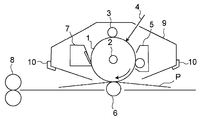
도 1은 전자 사진 감광체를 갖는 프로세스 카트리지를 구비한 전자 사진 장치의 개략 구성의 일례를 나타내는 도면.
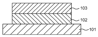
도 2a 및 도 2b는 전자 사진 감광체의 층 구성의 일례를 나타내는 도면.
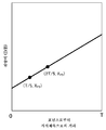
도 3은 전자 사진 감광체의 전하 수송층 중의 대표 2점인 XP2와 XP3의 관계의 일례를 나타내는 도면.
도 4는 전자 사진 감광체의 전하 수송층에서의 P1, P2, P3, P4 및 P5의 합계 5점의 위치 관계를 도시하는 도면.BRIEF DESCRIPTION OF THE DRAWINGS Fig. 1 is a view showing an example of a schematic configuration of an electrophotographic apparatus having a process cartridge having an electrophotographic photosensitive member. Fig.
2A and 2B are diagrams showing an example of the layer structure of the electrophotographic photosensitive member.
3 is a view showing an example of the relationship between X P2 and X P3 which are two representative points in the charge transport layer of the electrophotographic photosensitive member.
4 is a diagram showing the positional relationship of five points in total of P1, P2, P3, P4 and P5 in the charge transport layer of the electrophotographic photosensitive member.
본 발명의 다른 특징들은, 첨부된 도면들을 참조하여 이하의 예시적 실시형태들의 설명으로부터 명확해질 것이다.Other features of the present invention will become apparent from the following description of exemplary embodiments with reference to the accompanying drawings.
본 발명의 바람직한 실시형태를 첨부된 도면에 따라 상세히 설명한다.Preferred embodiments of the present invention will be described in detail with reference to the accompanying drawings.
본 발명은 전하 수송층이 식 4-1을 만족하는 것을 특징으로 한다.The present invention is characterized in that the charge transport layer satisfies Expression 4-1.
[식 4-1][Formula 4-1]
XP1 < XP5 X P1 < X P5
XP1은 P1에서의 적외 분광법에 의한 측정에 기초하여 얻어진 전하 수송 물질(D)과 결착 수지(B)의 질량비(D/B)를 나타내며,X P1 represents the mass ratio (D / B) of the charge transport material (D) and the binder resin (B) obtained based on the measurement by infrared spectroscopy at P1,
XP5는 P5에서의 적외 분광법에 의한 측정에 기초하여 얻어진 전하 수송 물질(D)과 결착 수지(B)의 질량비(D/B)를 나타내며,X P5 represents the mass ratio (D / B) of the charge transport material (D) and the binder resin (B) obtained on the basis of the measurement by infrared spectroscopy at P5,
P1은, 전하 수송층의 표면의 위치(전하 수송층의 막 두께를 T로 했을 때, 전하 수송층의 표면으로부터 0T/5=0의 거리에 있는 위치)이며,P1 is a position of the surface of the charge transport layer (a position at a distance of 0T / 5 = 0 from the surface of the charge transport layer when the film thickness of the charge transport layer is T)
P5는, 전하 수송층의 막 두께를 T로 했을 때, 전하 수송층의 표면으로부터 4T/5의 거리에 있는 위치이다.P5 is a position at a distance of 4T / 5 from the surface of the charge transport layer when the film thickness of the charge transport layer is T.
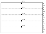
도 4는 전자 사진 감광체의 전하 수송층에서의 P1, P2, P3, P4, P5의 합계 5점의 위치 관계를 나타낸다. XP1 및 XP5는, 5점 중의 2점인 P1, P5에서의 전하 수송 물질(D)과 결착 수지(B)의 질량비(D/B)를 측정함으로써 구한다.4 shows the positional relationship of five points in total of P1, P2, P3, P4 and P5 in the charge transport layer of the electrophotographic photosensitive member. X P1 and X P5 are determined by measuring the mass ratio (D / B) between the charge transport material (D) and the binder resin (B) at P1 and P5 which are two out of five points.
상기의 특징은, 결착 수지에 대한 전하 수송 물질의 질량 비율이 전하 수송층의 지지체측(상기 P5의 위치)에서 전하 수송층의 표면측(전자 사진 감광체의 표면측)보다 높아지는(점증하고 있음) 구성을 전하 수송층(표면층)이 갖는 것을 의미한다. 본 발명자들은, 상기 특징에 의해, 화상 결함의 억제와 전위 변동의 억제가 양립하는 이유를 이하와 같이 추측하고 있다.The above-mentioned characteristic is that the mass ratio of the charge transporting material to the binder resin is higher (is increasing) than the surface side of the charge transport layer (the surface side of the electrophotographic photosensitive member) on the support side (position of P5) of the charge transport layer Means that the charge transport layer (surface layer) has. The inventors of the present invention presume the reason why the suppression of image defects and the suppression of potential fluctuations are compatible with each other as described below.
일반적으로, 전하 수송 물질은 전하를 수송하는 역할을 하며, 결착 수지는 전자 사진 감광체의 표면의 내마모성에 기여한다. 전하 수송층의 표면 근방에서는 결착 수지의 존재 비율이 높아짐으로써, 전하 수송층의 표면의 표면 저항이 높아짐으로써, 전자 사진 감광체의 반복 사용에 의한 화상 결함의 발생을 억제하고 있다.Generally, the charge transport material serves to transport charge, and the binder resin contributes to the abrasion resistance of the surface of the electrophotographic photosensitive member. The presence of the binder resin in the vicinity of the surface of the charge transport layer increases the surface resistance of the surface of the charge transport layer, thereby suppressing the occurrence of image defects caused by repeated use of the electrophotographic photosensitive member.
또한, 전하 수송층의 표면 근방에서는 결착 수지의 질량 비율이 높아짐으로써 내마모성(마모되기 어려움)이 향상된다. 그리고, 전하 수송층의 지지체측(전하 발생층과의 계면의 부근: P5)에서는 전하 수송 물질의 질량 비율이 높아짐으로써 전하 수송성이 효율적으로 발휘된다. 이 내마모성의 향상과 전하 수송성의 향상으로부터 전자 사진 감광체의 반복 사용 후의 전위 변동을 보다 억제하고 있다고 생각된다.In addition, in the vicinity of the surface of the charge transport layer, the abrasion resistance (hard to be worn) is improved by increasing the mass ratio of the binder resin. And, in the side of the support of the charge transport layer (in the vicinity of the interface with the charge generation layer: P5), the mass ratio of the charge transport material is increased, so that the charge transportability is efficiently exhibited. It is considered that the improvement of the abrasion resistance and the improvement of the charge transportability further suppress the potential fluctuation after repeated use of the electrophotographic photosensitive member.
본 발명의 전하 수송층이 식 4-2 내지 4-5를 만족하면, 화상 결함과 전위 변동이 보다 억제되기 때문에 바람직하다.When the charge transporting layer of the present invention satisfies the equations (4-2) to (4-5), it is preferable because the image defect and potential fluctuation are further suppressed.
[식 4-2] XP1 < XP2 [Expression 4-2] X P1 < X P2
[식 4-3] XP2 < XP3 [Formula 4-3] X P2 < X P3
[식 4-4] XP3 <XP4 [Formula 4-4] X P3 < X P4
[식 4-5] XP4 < XP5 [Formula 4-5] X P4 < X P5
식 4-2 내지 4-5 중,Of the formulas 4-2 to 4-5,
XP2는, P2에서의 적외 분광법에 의한 측정에 기초하여 얻어진 전하 수송 물질(D)과 결착 수지(B)의 질량비(D/B)를 나타내며,X P2 represents the mass ratio (D / B) of the charge transport material (D) and the binder resin (B) obtained based on the measurement by infrared spectroscopy at P2,
XP3은, P3에서의 적외 분광법에 의한 측정에 기초하여 얻어진 전하 수송 물질(D)과 결착 수지(B)의 질량비(D/B)를 나타내며,X P3 represents the mass ratio (D / B) of the charge transport material (D) and the binder resin (B) obtained based on the measurement by infrared spectroscopy at P3,
XP4는, P4에서의 적외 분광법에 의한 측정에 기초하여 얻어진 전하 수송 물질(D)과 결착 수지(B)의 질량비(D/B)를 나타내며,X P4 represents the mass ratio (D / B) of the charge transport material (D) and the binder resin (B) obtained based on the measurement by infrared spectroscopy at P4,
P2는, 전하 수송층의 막 두께를 T로 했을 때, 전하 수송층의 표면으로부터 T/5의 거리에 있는 위치이며,P2 is a position at a distance of T / 5 from the surface of the charge transport layer when the film thickness of the charge transport layer is T,
P3은, 전하 수송층의 막 두께를 T로 했을 때, 전하 수송층의 표면으로부터 2T/5의 거리에 있는 위치이며,P3 is a position at a distance of 2T / 5 from the surface of the charge transport layer when the film thickness of the charge transport layer is T,
P4는, 전하 수송층의 막 두께를 T로 했을 때, 전하 수송층의 표면으로부터 3T/5의 거리에 있는 위치이다.P4 is a position at a distance of 3T / 5 from the surface of the charge transport layer when the film thickness of the charge transport layer is T.
식 4-2 내지 4-5를 만족하면, P1로부터 P5의 위치를 향함에 따라, 전하 수송층의 질량 비율이 높아지는 구성을 취한다.When the formulas 4-2 to 4-5 are satisfied, a configuration is adopted in which the mass ratio of the charge transport layer increases as the position is shifted from the position P1 to the position P5.
전하 수송층의 전하 수송 물질의 농도 구배는, 도 3에 도시한 바와 같이 이하에 설명하는 구배일 있다. 구체적으로는, 전하 수송층은 식 5를 만족할 수 있다.The concentration gradient of the charge transporting material in the charge transporting layer may be a gradient described below as shown in Fig. Specifically, the charge transport layer can satisfy the expression (5).
[식 5][Formula 5]
0.020≤(XPm +1-XPm)/(mT/5-(m-1)T/5)≤0.060 0.020? (X Pm +1 -X Pm ) / (mT / 5- (m-1) T / 5)? 0.060
식 5 중, m은 1 내지 4의 정수이다.In formula (5), m is an integer of 1 to 4.
m=1일 때, 식 5는 식 5-1이 되며, m=2일 때, 식 5는 식 5-2가 되며, m=3일 때, 식 5는 식 5-3이 되며, m=4일 때, 식 5는 식 5-4가 된다. 즉, 전하 수송층은 식 5-1 내지 5-4를 만족한다.When m = 1, the
[식 5-1][Formula 5-1]
0.020≤(XP2-XP1)/(T/5-0)≤0.0600.020? (X P2 -X P1 ) / (T / 5-0)? 0.060
[식 5-2][Formula 5-2]
0.020≤(XP3-XP2)/(2T/5-T/5)≤0.0600.020? (X P3- X P2 ) / (2T / 5-T / 5)? 0.060
[식 5-3][Formula 5-3]
0.020≤(XP4-XP3)/(3T/5-2T/5)≤0.0600.020? (X P4 -X P3 ) / (3T / 5-2T / 5)? 0.060
[식 5-4][Equation 5-4]
0.020≤(XP5-XP4)/((4T/5-3T/5)≤0.0600.020? (X P5- X P4 ) / (4T / 5-3T / 5)? 0.060
전자 사진 감광체의 반복 사용 후의 화상 결함과 전위 변동을 보다 억제하기 때문에, 전하 수송층의 표면측으로부터 지지체측으로의 전하 수송 물질의 농도 구배의 기울기는 식 5의 범위 내 일 수 있다. The gradient of the concentration gradient of the charge transporting material from the surface side of the charge transporting layer to the support may be within the range of
[전하 수송층][Charge Transport Layer]
본 발명의 전자 사진 감광체의 전하 수송층은, 전하 수송 물질 및 결착 수지를 함유한다. 전하 수송 물질로서, 화학식 2 및 화학식 3으로 나타내는 화합물로 이루어지는 군에서 선택되는 적어도 1종의 전하 수송 물질을 함유한다. 결착 수지로서, 화학식 1A로 나타내는 구조 단위를 갖는 폴리카보네이트 수지 및 화학식 1B로 나타내는 구조 단위를 갖는 폴리에스테르 수지로 이루어지는 군에서 선택되는 적어도 1종의 결착 수지를 함유한다.The charge transport layer of the electrophotographic photoconductor of the present invention contains a charge transport material and a binder resin. As the charge transport material, at least one charge transport material selected from the group consisting of the compounds represented by formulas (2) and (3) is contained. The binder resin contains at least one kind of binder resin selected from the group consisting of a polycarbonate resin having a structural unit represented by the formula (1A) and a polyester resin having a structural unit represented by the formula (1B).
[화학식 2](2)

[화학식 3](3)

화학식 2 중, Ar21 및 Ar22는 각각 독립적으로 페닐기 또는 메틸기로 치환된 페닐기를 나타낸다. 화학식 3 중, Ar23 내지 Ar28은, 각각 독립적으로 페닐기 또는 메틸기로 치환된 페닐기를 나타낸다.In the general formula (2), Ar 21 and Ar 22 each independently represent a phenyl group or a phenyl group substituted with a methyl group. In the general formula (3), Ar 23 to Ar 28 each independently represent a phenyl group or a phenyl group substituted with a methyl group.
[화학식 1A]≪ EMI ID =

[화학식 1B]≪ RTI ID = 0.0 &

화학식 1A 중, R1 내지 R4는 각각 독립적으로 수소 원자, 메틸기 또는 페닐기를 나타내며, X1은 단결합, 산소 원자, 시클로헥실리덴기 또는 화학식 A로 나타내는 2가의 기를 나타낸다.In the formula (1A), R 1 to R 4 each independently represent a hydrogen atom, a methyl group or a phenyl group, and X 1 represents a single bond, an oxygen atom, a cyclohexylidene group or a bivalent group represented by the formula (A).
화학식 1B 중, R11 내지 R14는 각각 독립적으로 수소 원자, 메틸기 또는 페닐기를 나타내며, X2는 단결합, 산소 원자, 시클로헥실리덴기 또는 화학식 A로 나타내는 2가의 기를 나타내며, 또한, Y1은 m-페닐렌기, p-페닐렌기, 시클로헥실렌기 또는 화학식 B로 나타내는 2가의 기를 나타낸다.In the formula 1B, R 11 to R 14 each independently represent a hydrogen atom, a methyl group or a phenyl group, X 2 represents a divalent group represented by a single bond, an oxygen atom, a cyclohexylidene dengi) or (A, In addition, Y 1 is an m-phenylene group, a p-phenylene group, a cyclohexylene group or a bivalent group represented by the formula (B).
[화학식 A](A)

[화학식 B][Chemical Formula B]

화학식 A 중, R21 및 R22는 각각 독립적으로 수소 원자, 메틸기, 에틸기 또는 또는 페닐기를 나타낸다.In the formula (A), R 21 and R 22 each independently represent a hydrogen atom, a methyl group, an ethyl group or a phenyl group.
화학식 B 중, R31 내지 R38은 각각 독립적으로 수소 원자, 메틸기 또는 페닐기를 나타내며, X3은 단결합, 산소 원자, 황 원자 또는 메틸렌기를 나타낸다.In the formula (B), each of R 31 to R 38 independently represents a hydrogen atom, a methyl group or a phenyl group, and X 3 represents a single bond, an oxygen atom, a sulfur atom or a methylene group.
전하 수송 물질(D)과 결착 수지(B)의 질량비(D/B)는 적외 분광법에 의해 측정하고 IR(적외 분광) 장치가 사용된다. 예를 들어, 푸리에 변환형 적외 분광(FT-IR) 장치가 사용된다.The mass ratio (D / B) of the charge transport material (D) and the binder resin (B) is measured by infrared spectroscopy and IR (infrared spectroscopy) apparatus is used. For example, a Fourier transform infrared spectroscopy (FT-IR) device is used.
식 4-1 내지 4-5를 만족하는 전하 수송층은, 전하 수송 물질, 결착 수지와, 이하의 제1 용제와 제2 용제를 함유하는 전하 수송층용 도포액의 도막을 건조함으로써 형성된다. 그 외에, 23℃, 1 기압 환경 하에서의 전하 수송 물질의 제1 용제 100g에 대한 용해도를 Y1(g)로 하고, 전하 수송 물질의 제2 용제 100g에 대한 용해도를 Y2 (g)로 했을 때, 용해도 Y1과 용해도 Y2는 식 6을 만족한다.The charge transporting layer satisfying Formulas 4-1 to 4-5 is formed by drying a coating film of a charge transporting material, a binder resin and a coating solution for a charge transport layer containing the following first and second solvents. In addition, when the solubility of the charge transport material in 100 g of the first solvent in a 1 atm atmosphere at 23 DEG C is Y1 (g) and the solubility of the charge transport material in 100 g of the second solvent is Y2 (g) Y1 and solubility Y2 satisfy Equation (6).
[식 6] Y1 > Y2[Equation 6] Y1 > Y2
상기 제1 용제는, 톨루엔, 크실렌, 에틸벤젠 및 메시틸렌으로 이루어지는 군에서 선택되는 적어도 1종이다. 또한, 크실렌의 비점은 138 내지 144℃이고, 톨루엔의 비점은 110.6℃이고, 에틸벤젠의 비점은 136℃이고, 메시틸렌의 비점은 165℃이다.The first solvent is at least one selected from the group consisting of toluene, xylene, ethylbenzene and mesitylene. The boiling point of xylene is 138 to 144 占 폚, the boiling point of toluene is 110.6 占 폚, the boiling point of ethylbenzene is 136 占 폚, and the boiling point of mesitylene is 165 占 폚.
제2 용제는, 제1 용제보다 1 기압에서의 비점이 높은 화합물이다. 제1 용제보다 1 기압에서의 비점이 높은 화합물이란, 예를 들어 제1 용제가 톨루엔만을 함유하는 경우에는 톨루엔보다 1 기압에서의 비점이 높은 화합물이며, 제1 용제가 크실렌만을 함유하는 경우에는, 크실렌보다 1 기압에서의 비점이 높은 화합물이다. 제1 용제가 혼합 용제의 경우에는, 혼합 용제 중 가장 비점이 높은 화합물보다 비점이 높은 화합물이다. 예를 들어, 크실렌 및 톨루엔을 사용하는 경우에는, 크실렌보다 1 기압에서의 비점이 높은 화합물이 제2 용제에 해당한다.The second solvent is a compound having a high boiling point at 1 atm than the first solvent. A compound having a high boiling point at 1 atm than the first solvent means a compound having a high boiling point at 1 atm than toluene when the first solvent contains only toluene and when the first solvent contains only xylene, It is a compound with a high boiling point at 1 atm than xylene. When the first solvent is a mixed solvent, it is a compound having a boiling point higher than that of the compound having the highest boiling point among the mixed solvents. For example, when xylene and toluene are used, a compound having a high boiling point at 1 atm than xylene is the second solvent.
제2 용제의 후보가 되는 용제로서는, 예를 들어 디부틸에테르(비점: 142℃), 디-n-헥실 에테르(비점: 227℃), 부틸페닐 에테르(비점: 210.2℃), 아니솔(비점: 154℃), 페네톨(비점: 172℃), 4-메틸아니솔(비점: 174℃), 에틸 벤질 에테르(비점: 186℃), 디페닐 에테르(비점: 259℃), 디벤질 에테르(비점: 297℃), 1, 4-디메톡시벤젠(비점: 213℃), 시네올(비점: 176℃), 1, 2- 디부톡시에탄(비점: 203℃), 디에틸렌 글리콜 디메틸 에테르(비점: 162℃), 디에틸렌 글리콜 에틸 메틸 에테르(비점: 179℃), 에틸렌 글리콜 디에틸 에테르(비점: 189℃), 트리에틸렌 글리콜 디메틸 에테르(비점: 216℃), 디프로필렌 글리콜 디메틸 에테르(비점: 175℃), 디에틸렌 글리콜 디에틸 에테르(비점: 188℃), 디에틸렌 글리콜 디부틸 에테르(비점: 256℃), 1-헥산올(비점: 158℃), 1-헵탄올(비점: 176℃), 시클로헥산올(비점: 161℃), 벤질 알코올(비점: 205℃), 에틸렌 글리콜(비점: 197.3℃), 1, 4-부탄디올(비점: 230℃), 1, 5-펜탄디올(비점: 242℃), 디에틸렌 글리콜(비점: 244.3℃), 2-헵타논(비점: 151.5℃), 4-헵타논(비점: 143.7℃), 아세틸아세톤(비점: 140.4℃), 디이소부틸 케톤(비점: 163℃), 아세토닐아세톤(비점: 191℃), 포론(비점: 198℃), 아세토페논(비점: 202℃), 이소포론(비점: 215.3℃), 시클로헥사논(비점: 155.6℃), 메틸시클로헥사논(비점: 169℃), 아세트산 벤질(비점: 212℃), 아세트산 펜틸(비점: 149.2℃), 아세트산 이소펜틸(비점: 142.1℃), 3-메톡시부틸 아세테이트(비점: 172℃), 아세트산 2-에틸부틸(비점: 160℃), 아세트산 2-에틸헥실(비점: 198.6℃), 아세트산 시클로헥실(비점: 172℃), 아세트산 벤질(비점: 215.5℃), 벤조산 메틸(비점: 199.6℃), 벤조산 에틸(비점: 212℃), 프로피온산 부틸(비점: 146.8℃), 프로피온산 이소펜틸(비점: 160.7℃), 부티르산 부틸(비점: 166.6℃), 부티르산 이소펜틸(비점: 184.8℃), 옥살산 디에틸(비점: 188.5℃), 말론산 디에틸(비점: 199.3℃), 프탈산 디메틸(비점: 283℃), 살리실산 메틸(비점: 222℃), 3-에톡시 프로피온산 에틸(비점: 166℃), 에틸렌 글리콜 모노메틸 에테르 아세테이트(비점: 145℃), 에틸렌 글리콜 모노에틸 에테르 아세테이트(비점: 156.3℃), 프로필렌 글리콜 모노메틸 에테르 아세테이트(비점: 146℃), 에틸렌 글리콜 모노부틸 에테르 아세테이트(비점: 192℃), 에틸렌 글리콜 모노헥실 에테르 아세테이트(비점: 208.3℃), 디에틸렌 글리콜 모노에틸 에테르 아세테이트(비점: 217.4℃), γ-부티로락톤(비점: 204℃), 탄산 에틸렌(비점: 260.7℃), 탄산 프로필렌(비점: 240℃), 쿠멘(비점: 152.4℃), 테트랄린(비점: 207.5℃), 부틸벤젠(비점: 183.3℃), t-부틸벤젠(비점: 169℃), p-시멘(비점: 177.1℃), 시클로헥실벤젠(비점: 238.9℃), o-디에틸벤젠(비점: 183.5℃), 펜틸벤젠(비점: 205℃), 도데실벤젠(비점: 288℃), 노난(비점: 150.8℃), 데칸(비점: 174.2℃), N-메틸피롤리돈(비점: 202℃), 니트로벤젠(비점: 210.9℃), 술포란(비점: 285℃)을 들 수 있다.Examples of the solvent that is a candidate for the second solvent include dibutyl ether (boiling point: 142 ° C), di-n-hexyl ether (boiling point: 227 ° C), butyl phenyl ether (Boiling point: 174 占 폚), ethyl benzyl ether (boiling point: 186 占 폚), diphenyl ether (boiling point: 259 占 폚), dibenzyl ether (Boiling point: 297 占 폚), 1,4-dimethoxybenzene (boiling point: 213 占 폚), cineol (boiling point: 176 占 폚), 1,2-dibutoxyethane (boiling point: 203 占 폚), diethylene glycol dimethyl ether : 162 ° C), diethylene glycol ethyl methyl ether (boiling point: 179 ° C), ethylene glycol diethyl ether (boiling point: 189 ° C), triethylene glycol dimethyl ether (boiling point: 216 ° C), dipropylene glycol dimethyl ether 175 ° C), diethylene glycol diethyl ether (boiling point: 188 ° C), diethylene glycol dibutyl ether (boiling point: 256 ° C), 1-hexanol (boiling point: 158 ° C) ), Cyclohexanol ( (Boiling point: 242 占 폚), 1,6-hexanediol (boiling point: 242 占 폚), benzyl alcohol (boiling point: 205 占 폚), ethylene glycol Heptanone (boiling point: 143.7 占 폚), acetylacetone (boiling point: 140.4 占 폚), diisobutyl ketone (boiling point: 163 占 폚), ethylene glycol (boiling point: 244.3 占 폚), 2- , Acetonyl acetone (boiling point: 191 DEG C), poron (boiling point: 198 DEG C), acetophenone (boiling point: 202 DEG C), isophorone (boiling point: 215.3 DEG C), cyclohexanone (boiling point: 155.6 DEG C) Methoxybutyl acetate (boiling point: 172 占 폚), acetic acid (boiling point: 169 占 폚), benzyl acetate (boiling point: 212 占 폚), pentyl acetate (boiling point: 149.2 占 폚), isopentyl acetate Ethylhexyl acetate (boiling point: 198.6 占 폚), cyclohexyl acetate (boiling point: 172 占 폚), benzyl acetate (boiling point: 215.5 占 폚), methyl benzoate (boiling point: 199.6 占 폚) , Ethyl benzoate (boiling point: 212 占 폚), butyl propionate (boiling point: 1 46.8 占 폚), isopentyl propionate (boiling point: 160.7 占 폚), butyl butyrate (boiling point: 166.6 占 폚), isopentyl butyrate (boiling point: 184.8 占 폚), diethyl oxalate (boiling point: 188.5 占 폚) Ethylene glycol monomethyl ether acetate (boiling point: 145 占 폚), ethylene glycol (boiling point: 233 占 폚), dimethyl phthalate (boiling point: 283 占 폚), methyl salicylate (boiling point: 222 占 폚), ethyl 3-ethoxypropionate Propylene glycol monomethyl ether acetate (boiling point: 146 占 폚), ethylene glycol monobutyl ether acetate (boiling point: 192 占 폚), ethylene glycol monohexyl ether acetate (boiling point: 208.3 占 폚), monoethyl ether acetate Diethylene glycol monoethyl ether acetate (boiling point: 217.4 占 폚),? -Butyrolactone (boiling point: 204 占 폚), ethylene carbonate having a boiling point of 260.7 占 폚, propylene carbonate having a boiling point of 240 占 폚, cumene having a boiling point of 152.4 占 폚 ), Tetralin (boiling point: 207.5 DEG C), butylbenzene (boiling point: Cyclohexylbenzene (boiling point: 238.9 占 폚), o-diethylbenzene (boiling point: 183.5 占 폚), pentylbenzene (boiling point: (Boiling point: 205 占 폚), dodecylbenzene (boiling point: 288 占 폚), nonane (boiling point: 150.8 占 폚), decane (boiling point: 174.2 占 폚), N-methylpyrrolidone : 210.9 占 폚), and sulfolane (boiling point: 285 占 폚).
이들 화합물 중에서 상술한 용해도 Y1과 용해도 Y2에 관한 관계식을 만족하도록 제2 용제를 선택한다.The second solvent is selected so as to satisfy the above-described relational expression concerning the solubility Y1 and the solubility Y2.
제2 용제의 후보로서 용제의 예로서는, 바람직하게는, 헥산올, 헵탄올, 시클로헥산올, 벤질 알코올, 에틸렌 글리콜, 1, 4-부탄디올, 1, 5-펜탄디올, 디에틸렌 글리콜, 디에틸렌 글리콜 에틸 메틸 에테르, 탄산 에틸렌, 탄산 프로필렌, 니트로벤젠, 피롤리돈, N-메틸피롤리돈, 벤조산 메틸, 벤조산 에틸, 아세트산 벤질, 3-에톡시프로피온산 에틸, 아세토페논, 살리실산 메틸, 프탈산 디메틸 및 술포란을 들 수 있다.Examples of the solvent as a candidate for the second solvent are preferably hexanol, heptanol, cyclohexanol, benzyl alcohol, ethylene glycol, 1,4-butanediol, 1,5- pentanediol, diethylene glycol, diethylene glycol Ethyl methyl ether, ethyl carbonate, propylene carbonate, nitrobenzene, pyrrolidone, N-methylpyrrolidone, methyl benzoate, ethyl benzoate, benzyl acetate, ethyl 3-ethoxypropionate, acetophenone, methyl salicylate, dimethyl phthalate, It can be called a forran.
제1 용제 및 제2 용제를 함유하는 전하 수송층용 도포액의 도막을 건조시켜 전하 수송층을 형성함으로써, 전하 수송 물질과 결착 수지의 비율이 막 두께 방향으로 변화하고, 전하 수송층이 막 두께 방향으로의 전하 수송 물질의 농도 구배를 갖는다. 본 발명자들은, 전하 수송층이 막 두께 방향으로의 전하 수송 물질의 농도 구배를 갖는 이유를 이하와 같이 추측한다.The coating film for the charge transport layer containing the first solvent and the second solvent is dried to form the charge transport layer so that the ratio of the charge transport material to the binder resin changes in the film thickness direction and the charge transport layer moves in the film thickness direction And has a concentration gradient of the charge transport material. The present inventors speculate that the reason why the charge transporting layer has a concentration gradient of the charge transporting material in the thickness direction is as follows.
전하 수송층용 도포액의 도막을 건조시키는 공정에서, 지지체로부터의 열이 지지체(전하 발생층과의 계면)로부터 도막으로 전해짐으로써, 도막의 지지체측 부근의 용제가 증발한다. 제1 용제는, 제2 용제보다 비점이 낮기 때문에, 도막의 지지체측에서의 가열에 의해 제1 용제가 우선적으로 증발하는 것으로 생각된다. 본 발명에서는, 전하 수송 물질의 제1 용제에 대한 용해도 Y1은, 전하 수송 물질의 제2 용제에 대한 용해도 Y2보다 높다. 따라서, 가열에 의해 제1 용제가 제2 용제보다 우선적으로 증발하면, 도막의 지지체측에서 도막 내의 제1 용제의 양이 제2 용제의 양에 비하여 감소하게 된다고 생각된다. 그 결과, 전부 용해될 수 없게 된 전하 수송 물질이 도막의 지지체측에서 석출된다고 생각된다.In the step of drying the coating film for the charge transport layer, heat from the support is transferred to the coating film from the support (interface with the charge generating layer), whereby the solvent near the support side of the coating film evaporates. Since the boiling point of the first solvent is lower than that of the second solvent, it is considered that the first solvent is preferentially evaporated by heating on the support side of the coating film. In the present invention, the solubility Y1 of the charge transport material to the first solvent is higher than the solubility Y2 of the charge transport material to the second solvent. Therefore, when the first solvent is preferentially evaporated by heating, the amount of the first solvent in the coating film on the support side of the coating film is thought to be smaller than the amount of the second solvent. As a result, it is considered that the charge-transporting material which can not be completely dissolved precipitates on the support side of the coating film.
또한, 도막의 건조가 진행하면, 도막의 고형분 농도가 경시적으로 높아지면서, 전하 수송층이 형성되어 간다. 또한, 건조 과정에 있는 도막 내의 제1 용제의 함유 비율은 서서히 낮아진다. 그 결과, 제1 용제의 함유 비율의 경시적인 감소에 수반하여, 전하 수송 물질이 석출된다. 제1 용제와 제2 용제의 비율의 연속적인 변화와, 전하 수송 물질의 제1 용제에 대한 용해도와 제2 용제에 대한 용해도의 차를 이용함으로써 전하 수송층 중의 전하 수송 물질의 농도에 구배를 갖게 할 수 있다고 본 발명자들은 생각되었다. 또한, 결착 수지인 폴리카보네이트 수지 및/또는 폴리에스테르 수지의 제1 용제에 대한 용해도와 제2 용제에 대한 용해도의 차는, 상술한 전하 수송 물질의 제1 용제에 대한 용해도와 제2 용제에 대한 용해도의 차보다는 비교적 작다. 따라서, 전하 수송 물질의 제1 용제에 대한 용해도와 제2 용제에 대한 용해도의 차에 의해, 막 두께 방향으로의 전하 수송 물질의 농도 구배를 갖는 전하 수송층이 형성된다고 생각되었다.When the drying of the coating film progresses, the solid content of the coating film becomes higher with time, and the charge transporting layer is formed. In addition, the content ratio of the first solvent in the coating film in the drying process is gradually lowered. As a result, as the content ratio of the first solvent decreases with time, the charge transport material precipitates. A difference in the ratio of the first solvent to the second solvent is continuously changed and the difference between the solubility of the charge transport material in the first solvent and the solubility in the second solvent is used so that the concentration of the charge transport material in the charge transport layer is made to have a gradient The present inventors have thought. The difference between the solubility of the polycarbonate resin and / or the polyester resin as the binder resin in the first solvent and the solubility in the second solvent depends on the solubility of the charge transport material in the first solvent and the solubility in the second solvent Is relatively small. Therefore, it was thought that the charge transporting layer having a concentration gradient of the charge transporting material in the film thickness direction was formed by the difference between the solubility of the charge transporting material in the first solvent and the solubility in the second solvent.
화상 결함의 억제와 반복 사용 후의 전위 안정성을 높은 레벨로 양립할 수 있기 때문에, 전하 수송층용 도포액에서 제1 용제의 함유량이 제2 용제의 함유량보다도 많을 수 있다.The content of the first solvent in the coating liquid for the charge transport layer may be higher than the content of the second solvent since the suppression of image defects and the dislocation stability after repeated use can be made compatible at a high level.
[전하 수송 물질][Charge transport material]
전하 수송 물질은, 화학식 2로 나타내는 화합물 및/또는 화학식 3으로 나타내는 화합물이다. 전하 수송 물질의 구체예를 이하에 나타낸다.The charge transport material is a compound represented by the formula (2) and / or a compound represented by the formula (3). Specific examples of the charge transport material are shown below.

이들 화합물 중에서 Y1>Y2의 관계를 고려하여 전하 수송 물질이 선택된다. 본 발명에 사용되는 전하 수송 물질은, 1종만이 화합물이어도 되고, 2종 이상의 화합물이어도 된다.Among these compounds, the charge transport material is selected in consideration of the relationship of Y1 > Y2. The charge transport material used in the present invention may be a single compound or two or more compounds.
[결착 수지][Binder resin]
결착 수지는, 화학식 1A로 나타내는 구조 단위를 갖는 폴리카보네이트 수지 및 화학식 1B로 나타내는 구조 단위를 갖는 폴리에스테르 수지로 이루어지는 군에서 선택되는 적어도 1종이다.The binder resin is at least one selected from the group consisting of a polycarbonate resin having a structural unit represented by the formula (1A) and a polyester resin having a structural unit represented by the formula (1B).
이하에, 화학식 1A로 나타내는 구조 단위를 갖는 폴리카보네이트 수지의 구조 단위의 구체예를 나타낸다.Specific examples of the structural unit of the polycarbonate resin having the structural unit represented by the formula (1A) are shown below.

특히, 구조 단위는 식 (1-1), (1-2), (1-4), (1-5) 중 어느 하나로 나타내는 구조 단위일 수 있다. 또한, 이들 구조 단위들 중 하나가 단독으로 사용될 수 있으며, 또는 혼합 또는 공중합체로서 2종 이상의 구조 단위가 사용될 수 있다. 그 공중합 형태는, 블록 공중합, 랜덤 공중합, 교대 공중합 등의 어느 형태이어도 된다. In particular, the structural unit may be a structural unit represented by any one of formulas (1-1), (1-2), (1-4) and (1-5). In addition, one of these structural units may be used alone, or two or more structural units may be used as a mixture or a copolymer. The copolymerization may take any form such as block copolymerization, random copolymerization, and alternating copolymerization.
이하에, 화학식 1B로 나타내는 구조 단위를 갖는 폴리에스테르 수지의 구조 단위의 구체예를 나타낸다.Specific examples of the structural unit of the polyester resin having the structural unit represented by the formula (1B) are shown below.


특히, 구조 단위는 화학식 (1-10), (1-11), (1-12), (1-15), (1-16), (1-17), (1-18) 중 어느 하나로 나타내는 구조 단위일 수 있다. 또한, 이들 구조 단위들 중 하나가 단독으로 사용될 수 있으며, 또는 혼합 또는 공중합체로서 구조 단위들 중 2종 이상이 사용될 수 있다. 그 공중합 형태는, 블록 공중합, 랜덤 공중합, 교대 공중합 등의 어느 형태이어도 된다.In particular, the structural unit may be any one of the structural formulas (1-10), (1-11), (1-12), (1-15), (1-16), (1-17) Lt; / RTI > In addition, one of these structural units may be used alone, or two or more structural units may be used as a mixture or copolymer. The copolymerization may take any form such as block copolymerization, random copolymerization, and alternating copolymerization.
화학식 1A로 나타내는 구조 단위를 갖는 폴리카보네이트 수지, 및 화학식 1B로 나타내는 구조 단위를 갖는 폴리에스테르 수지는 실록산 구조를 갖지 않을 수 있다. 또한, 전하 수송층은, 실록산 구조를 갖는 어떠한 폴리카보네이트 수지, 및 실록산 구조를 갖는 어떠한 폴리에스테르 수지를 함유하지 않을 수 있다. 여기서, 실록산 구조란, 실록산 부분을 구성하는 양단의 규소 원자 및 그들에 결합하는 기와, 상기 양단의 규소 원자에 끼워진 산소 원자, 규소 원자 및 그들에 결합하는 기를 갖는 구조이다. 구체적으로 말하면, 실록산 구조란, 이하에 나타내는 화학식 D-S에서 나타내는 점선의 범위내의 구조를 말한다. 화학식 D-S 중, a는 괄호내의 구조의 반복수를 나타내고, 수지에서의 a의 평균값은 1 이상 500 이하이다.The polycarbonate resin having a structural unit represented by the formula (1A) and the polyester resin having a structural unit represented by the formula (1B) may not have a siloxane structure. Further, the charge transport layer may not contain any polycarbonate resin having a siloxane structure and any polyester resin having a siloxane structure. Here, the siloxane structure is a structure having silicon atoms at both ends constituting the siloxane moiety and a group bonding to them, oxygen atoms sandwiched between silicon atoms at both ends, silicon atoms and groups bonded thereto. Specifically, the siloxane structure refers to a structure within the range indicated by the dotted line in the following chemical formula D-S. In formula (D-S), a represents the number of repeats of the structure in parentheses, and the average value of a in the resin is 1 or more and 500 or less.
[화학식 D-S][Chemical formula DS]

화학식 1A로 나타내는 구조 단위를 갖는 폴리카보네이트 수지, 및 화학식 1B로 나타내는 구조 단위를 갖는 폴리에스테르 수지는, 공지된 방법에 의해 합성할 수 있다. 상기 폴리카보네이트 수지는, 포스겐법이나 에스테르 교환법에 의해 합성될 수 있다. 상기 폴리에스테르 수지는, 예를 들어 일본 특허 공개 제2007-047655호 공보 및 일본 특허 공개 제2007-72277호 공보에 기재된 방법으로 합성할 수 있다. 상기 폴리카보네이트 수지 및 폴리에스테르 수지의 중량 평균 분자량으로서는, 20,000 이상 300,000 이하가 바람직하고, 보다 바람직하게는 50,000 이상 200,000 이하이다.The polycarbonate resin having the structural unit represented by the formula (1A) and the polyester resin having the structural unit represented by the formula (1B) can be synthesized by a known method. The polycarbonate resin can be synthesized by a phosgene method or an ester exchange method. The polyester resin can be synthesized by the method described in, for example, Japanese Patent Laid-Open Nos. 2007-047655 and 2007-72277. The weight average molecular weight of the polycarbonate resin and the polyester resin is preferably from 20,000 to 300,000, more preferably from 50,000 to 200,000.
본 발명에서, 수지의 중량 평균 분자량은, 통상법에 따라, 일본 특허 공개 제2007-79555호 공보에 기재된 방법에 의해 측정된 폴리스티렌 환산의 중량 평균 분자량이다.In the present invention, the weight average molecular weight of the resin is the weight average molecular weight in terms of polystyrene measured by the method described in Japanese Patent Application Laid-Open No. 2007-79555 according to a conventional method.
전하 수송층용 도포액에는, 1 기압에서의 비점이 35 내지 70℃인 화합물을 더 함유시켜도 된다. 상술한 바와 같이 제1 용제나 제2 용제보다 비점이 낮은 화합물을 함유시킴으로써, 전하 수송층용 도포액의 도막의 건조 초기에 있어 화합물이 우선적으로 증발하고, 전하 수송층의 표면 부근에서 열교환(흡열)이 일어나, 수지의 질량 비율이 높아진다. 이에 의해, 식 5를 기울기의 범위 내로 할 수 있다고 생각되었다. 1 기압에서의 비점이 35 내지 70℃인 화합물을, 아세톤(비점: 56.5℃), 디에틸 에테르(비점: 35℃), 아세트산 메틸(비점: 56.9℃), 테트라히드로푸란(비점: 66℃), 또는 디메톡시메탄(비점: 42℃)으로 할 수 있다.The coating liquid for the charge transport layer may further contain a compound having a boiling point of 35 to 70 DEG C at 1 atm. By containing a compound having a lower boiling point than the first solvent or the second solvent as described above, the compound is preferentially evaporated at the initial stage of drying of the coating film for the charge transport layer, and heat exchange (endotherm) is generated near the surface of the charge transport layer So that the mass ratio of the resin increases. By this, it was thought that the
전하 수송층에 첨가제를 함유시켜도 된다. 예를 들어, 이하의 같은 화합물(산화 방지제)을 들 수 있다. t-Bu는 tert-부틸기를 나타낸다.An additive may be contained in the charge transport layer. For example, the following compounds (antioxidants) can be mentioned. t-Bu represents a tert-butyl group.

전자 사진 감광체의 구성에 대해 설명한다. 본 발명의 전자 사진 감광체는, 지지체, 상기 지지체 상에 형성된 전하 발생층, 및 전하 발생층 상에 형성된 전하 수송층을 포함하고, 전하 수송층이 표면층이다. 전하 수송층을 적층 구조로 해도 되고, 이 경우, 표면측의 전하 수송층은 전하 수송 물질의 농도 구배를 갖는다. 도 2a 및 도 2b는 전자 사진 감광체의 층 구성의 일례를 나타내는 도면이다. 도 2a 및 도 2b 중, 참조부호 "101"은 지지체이며, "102"는 전하 발생층이며, "103"은 전하 수송층(제1 전하 수송층)이며, "104"는 제2 전하 수송층이다.The configuration of the electrophotographic photosensitive member will be described. The electrophotographic photosensitive member of the present invention comprises a support, a charge generating layer formed on the support, and a charge transporting layer formed on the charge generating layer, wherein the charge transporting layer is a surface layer. The charge transport layer may have a laminated structure. In this case, the charge transport layer on the surface side has a concentration gradient of the charge transport material. 2A and 2B are diagrams showing an example of the layer structure of the electrophotographic photosensitive member. In FIGS. 2A and 2B,
[지지체][Support]
지지체는, 도전성을 갖는 것(도전성 지지체)일 수 있다. 예를 들어, 알루미늄, 알루미늄 합금, 스테인리스 등의 금속제의 지지체를 사용할 수 있다. 알루미늄이나 알루미늄 합금제의 지지체의 경우에는, ED관, EI관이나, 또는 이들을 절삭, 전해 복합 연마(전해 작용을 갖는 전극과 전해질 용액에 의한 전해 및 연마 작용을 갖는 지석에 의한 연마), 습식 또는 건식 호닝 처리한 지지체를 사용할 수도 있다. 또한, 알루미늄, 알루미늄 합금 또는 산화인듐-산화주석 합금을 진공 증착에 의해 피막 형성된 층을 갖는 금속제 지지체나 수지제 지지체를 사용할 수도 있다.The support may be one having conductivity (conductive support). For example, metal supports such as aluminum, aluminum alloy, and stainless steel can be used. In the case of a support made of aluminum or an aluminum alloy, the ED tube, the EI tube, or a combination of them can be used for cutting, electrolytic compound polishing (polishing with electrolytic and electrolytic solution electrolytic solution and polishing stone having a polishing action) A dry-honed support may also be used. In addition, a metallic support or a resin support having a film-formed layer formed by vacuum evaporation of aluminum, an aluminum alloy, or an indium oxide-tin oxide alloy may be used.
또한, 카본 블랙, 산화주석 입자, 산화티타늄 입자, 은 입자와 같은 도전성 입자를 수지에 함침한 지지체나, 도전성 결착 수지를 갖는 플라스틱을 사용할 수도 있다.It is also possible to use a support impregnated with a conductive particle such as carbon black, tin oxide particles, titanium oxide particles or silver particles, or a plastic having a conductive binder resin.
지지체의 표면은, 레이저광 등의 산란으로 인한 간섭 줄무늬의 억제 등을 목적으로, 절삭 처리, 조면화 처리, 알루마이트 처리를 실시해도 된다.The surface of the support may be subjected to a cutting treatment, a roughening treatment or an alumite treatment for the purpose of suppressing interference fringes due to scattering of laser light or the like.
지지체의 표면이 도전성을 부여하기 위하여 설치된 층인 경우, 그 층의 체적 저항률은, 1×10¹⁰Ω·cm 이하인 것이 바람직하고, 특히, 1×10⁶Ω·cm 이하인 것이 보다 바람직하다.If the surface of the support layer, which used to impart conductivity, the volume resistivity of the layer is preferably not more than 1 × 10 10 Ω · cm, and particularly, more preferably not more than 1 × 10 6 Ω · cm.
전자 사진 감광체에 있어서, 지지체 상에, 레이저광 등의 산란으로 인한 간섭 줄무늬의 억제나, 지지체의 흠집의 피복을 목적으로 도전층을 설치해도 된다. 도전층은, 도전성 입자를 결착 수지에 분산시킨 도전층용 도포액의 도막을 건조시켜 형성되는 층이다.In the electrophotographic photosensitive member, a conductive layer may be provided on the support for the purpose of suppressing interference fringes due to scattering of laser light or the like, or for covering flaws on the support. The conductive layer is a layer formed by drying a coating film of a coating liquid for a conductive layer in which conductive particles are dispersed in a binder resin.
도전성 입자로서는, 예를 들어 카본 블랙, 아세틸렌 블랙이나, 알루미늄, 니켈, 철, 니크롬, 구리, 아연, 은과 같은 금속 분체나, 도전성 산화주석, ITO와 같은 금속 산화물 분체를 들 수 있다.Examples of the conductive particles include carbon black, acetylene black, metal powders such as aluminum, nickel, iron, nichrome, copper, zinc and silver, and metal oxide powders such as conductive tin oxide and ITO.
결착 수지로서는, 예를 들어 폴리에스테르 수지, 폴리카보네이트 수지, 폴리비닐부티랄 수지, 아크릴 수지, 실리콘 수지, 에폭시 수지, 멜라민 수지, 우레탄 수지, 페놀 수지, 알키드 수지를 들 수 있다.Examples of the binder resin include a polyester resin, a polycarbonate resin, a polyvinyl butyral resin, an acrylic resin, a silicone resin, an epoxy resin, a melamine resin, a urethane resin, a phenol resin and an alkyd resin.
도전층용 도포액의 용제로서는, 예를 들어 에테르계 용제, 알코올계 용제, 케톤계 용제, 방향족 탄화수소 용제 등을 들 수 있다.Examples of the solvent of the coating liquid for the conductive layer include ether solvents, alcohol solvents, ketone solvents, aromatic hydrocarbon solvents and the like.
도전층의 막 두께는, 0.2 ㎛ 이상 40 ㎛ 이하인 것이 바람직하고, 1 ㎛ 이상 35 ㎛ 이하인 것이 보다 바람직하고, 나아가 5 ㎛ 이상 30 ㎛ 이하인 것이 보다 바람직하다.The conductive layer preferably has a thickness of 0.2 to 40 탆, more preferably 1 to 35 탆, and further more preferably 5 to 30 탆.
지지체 또는 도전층과, 전하 발생층과의 사이에 언더 코팅층을 설치해도 된다. 언더 코팅층은, 결착 수지를 함유하는 언더 코팅층용 도포액의 도막을 지지체상 또는 도전층 상에 도포하고, 도막을 건조 또는 경화시킴으로써 형성할 수 있다.An undercoat layer may be provided between the support or the conductive layer and the charge generation layer. The undercoat layer can be formed by applying a coating film of a coating liquid for an undercoat layer containing a binder resin on a support or a conductive layer and drying or curing the coating film.
언더 코팅층의 결착 수지로서는, 예를 들어 폴리아크릴산류, 메틸셀룰로오스, 에틸셀룰로오스, 폴리아미드 수지, 폴리이미드 수지, 폴리아미드이미드 수지, 폴리아미드산 수지, 멜라민 수지, 에폭시 수지, 폴리우레탄 수지를 들 수 있다. 언더 코팅층에 사용되는 결착 수지는 열가소성 수지일 수 있다. 구체적으로, 결착 수지는 열가소성의 폴리아미드 수지일 수 있다. 폴리아미드 수지로서는, 용액 상태에서 도포할 수 있는 저결정성 또는 비결정성의 공중합 나일론일 수 있다.Examples of the binder resin for the undercoat layer include polyacrylic acids, methyl cellulose, ethyl cellulose, polyamide resin, polyimide resin, polyamideimide resin, polyamide acid resin, melamine resin, epoxy resin and polyurethane resin have. The binder resin used for the undercoat layer may be a thermoplastic resin. Specifically, the binder resin may be a thermoplastic polyamide resin. The polyamide resin may be low-crystalline or amorphous copolymerized nylon that can be applied in a solution state.
언더 코팅층의 막 두께는, 0.05 ㎛ 이상 40 ㎛ 이하인 것이 바람직하고, 보다 바람직하게는 0.05 ㎛ 이상 7 ㎛ 이하, 나아가 0.1 ㎛ 이상 2 ㎛ 이하인 것이 보다 바람직하다.The film thickness of the undercoat layer is preferably 0.05 mu m or more and 40 mu m or less, more preferably 0.05 mu m or more and 7 mu m or less, further preferably 0.1 mu m or more and 2 mu m or less.
또한, 언더 코팅층에서 전하(캐리어)의 흐름을 저해하지 않게 하기 위해서, 언더 코팅층에는, 반도전성 입자 또는 전자 수송 물질(억셉터와 같은 전자 수용성 물질)을 함유시켜도 된다.In order to prevent the flow of charge (carrier) in the undercoat layer, the undercoat layer may contain semiconductive particles or an electron transport material (an electron-accepting material such as an acceptor).
[전하 발생층][Charge generating layer]
지지체, 도전층 또는 언더 코팅층 상에는 전하 발생층이 형성된다.A charge generation layer is formed on a support, a conductive layer or an undercoat layer.
전자 사진 감광체에 사용되는 전하 발생 물질로서는, 예를 들어 아조 안료, 프탈로시아닌 안료, 인디고 안료, 페릴렌 안료 등을 들 수 있다. 본 발명에 사용되는 전하 발생 물질은, 1종만의 화합물로 이루어져 있어도 되고, 2종 이상의 화합물로 이루어져 있어도 된다. 전하 발생 물질로서 바람직하게 사용되는 화합물은, 고감도의 관점으로부터, 옥시티타늄 프탈로시아닌, 히드록시갈륨 프탈로시아닌, 클로로갈륨 프탈로시아닌 등일 수 있다.Examples of the charge generating material used in the electrophotographic photosensitive member include azo pigments, phthalocyanine pigments, indigo pigments and perylene pigments. The charge generating material used in the present invention may be composed of only one kind of compound or two or more kinds of compounds. From the viewpoint of high sensitivity, the compound preferably used as the charge generating material can be oxytitanium phthalocyanine, hydroxygallium phthalocyanine, chlorogallium phthalocyanine, and the like.
전하 발생층에 사용되는 결착 수지로서는, 예를 들어 폴리카보네이트 수지, 폴리에스테르 수지, 부티랄 수지, 폴리비닐 아세탈 수지, 아크릴 수지, 아세트산 비닐 수지, 요소 수지 등을 들 수 있다. 이들 결착 수지 중에서도, 전하 수송층용 도포액의 도포 시공성의 관점에서, 폴리카보네이트 수지 및 폴리에스테르 수지 이외의 수지가 바람직하고, 특히, 부티랄 수지가 보다 바람직하다. 이들 수지 중 하나가 단독으로 사용될 수 있으며, 또는 2종 이상의 수지가 혼합 또는 공중합체로서 사용될 수 있다.Examples of the binder resin used for the charge generation layer include polycarbonate resin, polyester resin, butyral resin, polyvinyl acetal resin, acrylic resin, vinyl acetate resin and urea resin. Of these binder resins, resins other than the polycarbonate resin and the polyester resin are preferable from the viewpoint of coating workability of the coating liquid for the charge transport layer, and a butyral resin is particularly preferable. Either one of these resins may be used alone, or two or more resins may be used as a mixture or a copolymer.
전하 발생층은, 전하 발생 물질을 결착 수지 및 용제와 함께 분산하여 얻어지는 전하 발생층용 도포액의 도막을 형성하고, 도막을 건조시킴으로써 형성할 수 있다. 또한, 전하 발생층은, 전하 발생 물질의 증착막일 수도 있다.The charge generation layer can be formed by forming a coating film of a coating liquid for a charge generation layer obtained by dispersing a charge generating material together with a binder resin and a solvent and drying the coating film. Further, the charge generation layer may be a vapor deposition film of the charge generation material.
분산 방법으로서는, 예를 들어 호모게나이저, 초음파, 볼 밀, 샌드밀, 아트라이터, 롤밀을 사용한 방법을 들 수 있다.Examples of the dispersion method include a homogenizer, an ultrasonic wave, a ball mill, a sand mill, an attritor, and a method using a roll mill.
전하 발생 물질과 결착 수지와의 비율은, 1: 10 내지 10: 1(질량비)의 범위가 바람직하고, 특히 1: 1 내지 3: 1(질량비)의 범위가 보다 바람직하다.The ratio of the charge generating material to the binder resin is preferably in the range of 1:10 to 10: 1 (mass ratio), more preferably in the range of 1: 1 to 3: 1 (mass ratio).
전하 발생층용 도포액에 사용되는 용제는, 예를 들어 알코올계 용제, 술폭시드계 용제, 케톤계 용제, 에테르계 용제, 에스테르계 용제 또는 방향족 탄화수소 용제 등을 들 수 있다.Examples of the solvent used in the coating liquid for the charge generation layer include alcohol solvents, sulfoxide solvents, ketone solvents, ether solvents, ester solvents and aromatic hydrocarbon solvents.
전하 발생층의 막 두께는, 5 ㎛ 이하인 것이 바람직하고, 0.1 ㎛ 이상 2 ㎛ 이하인 것이 보다 바람직하다.The film thickness of the charge generation layer is preferably 5 占 퐉 or less, more preferably 0.1 占 퐉 or more and 2 占 퐉 or less.
또한, 전하 발생층에는, 다양한 감광제, 산화 방지제, 자외선 흡수제, 가소제 등을 필요에 따라 첨가할 수도 있다. 또한, 전하 발생층에서 전하(캐리어)의 흐름을 저하하지 않게 하기 위해서, 전하 발생층에는, 전자 수송 물질(억셉터와 같은 전자 수용성 물질)을 함유시켜도 된다.Various photo-sensitizers, antioxidants, ultraviolet absorbers, plasticizers, and the like may be added to the charge generation layer as needed. The electron-transporting material (an electron-accepting material such as an acceptor) may be contained in the charge-generating layer in order not to lower the flow of charge (carrier) in the charge-generating layer.
[전하 수송층][Charge Transport Layer]
전하 발생층 상에는 전하 수송층이 설치된다.A charge transport layer is provided on the charge generation layer.
전하 수송층은, 상기 전하 수송 물질 및 상기 결착 수지를 함유한다. 전하 수송층을 형성하기 위한 전하 수송층용 도포액은, 전하 수송 물질 및 결착 수지 외에, 제1 용제 및 제2 용제를 함유한다.The charge transport layer contains the charge transport material and the binder resin. The coating liquid for the charge transport layer for forming the charge transport layer contains a first solvent and a second solvent in addition to the charge transport material and the binder resin.
전하 수송 물질과 결착 수지의 비율은, 3: 10 내지 20: 10(질량비)의 범위가 바람직하고, 5: 10 내지 15: 10(질량비)의 범위가 보다 바람직하다.The ratio of the charge transport material to the binder resin is preferably in the range of 3:10 to 20:10 (mass ratio), more preferably in the range of 5:10 to 15:10 (mass ratio).
전하 수송층의 막 두께는, 5 ㎛ 이상 50 ㎛ 이하인 것이 바람직하고, 10 ㎛ 이상 35 ㎛ 이하인 것이 보다 바람직하고, 10 ㎛ 이상 20 ㎛ 이하가 보다 바람직하다.The film thickness of the charge transporting layer is preferably 5 mu m or more and 50 mu m or less, more preferably 10 mu m or more and 35 mu m or less, and more preferably 10 mu m or more and 20 mu m or less.
전자 사진 감광체의 각 층에는 각종 첨가제를 첨가할 수 있다. 첨가제로서는, 예를 들어 산화 방지제, 자외선 흡수제, 내광 안정제와 같은 열화 방지제나, 유기 미립자 및 무기 미립자 등의 미립자를 들 수 있다. 열화 방지제로서는, 예를 들어 힌더드 페놀계 산화 방지제, 힌더드 아민계 내광 안정제, 황 원자 함유 산화 방지제, 인 원자 함유 산화 방지제를 들 수 있다. 유기 미립자로서는, 예를 들어 불소 원자 함유 수지 입자, 폴리스티렌 미립자, 폴리에틸렌 수지 입자와 같은 고분자 수지 입자를 들 수 있다. 무기 미립자로서는, 예를 들어 실리카, 알루미나와 같은 금속 산화물을 들 수 있다.Various additives may be added to each layer of the electrophotographic photosensitive member. Examples of additives include antioxidants such as antioxidants, ultraviolet absorbers and light stabilizers, and fine particles such as organic fine particles and inorganic fine particles. Examples of the deterioration inhibitor include hindered phenol-based antioxidants, hindered amine-based light stabilizers, sulfur atom-containing antioxidants and phosphorus atom-containing antioxidants. Examples of the organic fine particles include polymer resin particles such as fluorine atom-containing resin particles, polystyrene fine particles, and polyethylene resin particles. Examples of the inorganic fine particles include metal oxides such as silica and alumina.
상기 각 층에 도포액을 도포할 때에는, 침지 도포법(침지 코팅법), 스프레이 코팅법, 스피너 코팅법, 롤러 코팅법, 메이어 바 코팅법, 블레이드 코팅법과 같은 도포 방법을 사용할 수 있다. 특히, 그 중에서도 침지 도포법이 사용될 수 있다.When applying the coating liquid to each of the above layers, a coating method such as an immersion coating method (immersion coating method), a spray coating method, a spinner coating method, a roller coating method, a Meyer bar coating method and a blade coating method may be used. In particular, an immersion coating method may be used.
각 층의 건조 온도로서는, 60℃ 이상 150℃ 이하일 수 있다. 전하 수송층의 건조 온도로서는, 특히 100℃ 이상 140℃ 이하일 수 있다. 또한, 건조 시간으로서는, 10 내지 60분간이 바람직하고, 20 내지 60분간이 보다 바람직하다.The drying temperature of each layer may be 60 ° C or more and 150 ° C or less. The drying temperature of the charge transport layer may be in particular 100 ° C or more and 140 ° C or less. The drying time is preferably 10 to 60 minutes, more preferably 20 to 60 minutes.
[전자 사진 장치][Electrophotographic apparatus]
도 1에, 본 발명의 전자 사진 감광체를 갖는 프로세스 카트리지를 구비한 전자 사진 장치의 개략 구성의 일례를 나타낸다.Fig. 1 shows an example of a schematic configuration of an electrophotographic apparatus provided with a process cartridge having the electrophotographic photosensitive member of the present invention.
도 1에 있어서, 참조 부호 "1"은 원통 형상의 전자 사진 감광체를 나타내며, 원통 형상의 전자 사진 감광체는, 축(2)을 중심으로 화살표 방향으로 미리 정해진 원주 속도로 회전 구동된다. 회전 구동되는 전자 사진 감광체(1)의 표면은, 대전 수단(1차 대전 디바이스: 대전 롤러 등)(3)에 의해, 플러스 또는 마이너스의 미리 정해진 전위로 균일하게 대전된다. 계속해서, 상기 표면은, 슬릿 노광이나 레이저 빔 주사 노광 등의 노광 디바이스(도시하지 않음)로부터 출력되는 목적으로 하는 화상 정보의 시계열 전기 디지털 화상 신호에 따라 강도 변조된 노광광(화상 노광광)(4)을 받는다. 이렇게 하여 전자 사진 감광체(1)의 표면에, 원하는 화상에 따른 정전 잠상이 순차 형성되어 간다.1, reference numeral "1 " denotes a cylindrical electrophotographic photosensitive member, and a cylindrical electrophotographic photosensitive member is rotationally driven at a predetermined circumferential velocity in the direction of the arrow about the shaft 2. The surface of the rotationally driven electrophotographic
전자 사진 감광체(1)의 표면에 형성된 정전 잠상은, 현상 디바이스(5)의 현상제에 포함되는 토너로 반전 현상에 의해 현상되어 토너상이 형성된다. 계속해서, 전자 사진 감광체(1)의 표면에 형성 담지되어 있는 토너상은, 전사 디바이스(전사 롤러 등)(6)로부터의 전사 바이어스에 의해, 전사재(종이 등) P에 순차적으로 전사되어 간다. 또한, 전사재 P는, 전사재 공급 디바이스(도시하지 않음)로부터 전자 사진 감광체(1)와 전사 디바이스(6)의 사이의 부분(접촉부)으로 전자 사진 감광체(1)의 회전과 동기하여 취출되어 급송된다. 또한, 전사 디바이스(6)에는, 바이어스 전원(도시하지 않음)으로부터 토너의 전하와는 역극성의 바이어스 전압이 인가된다.The electrostatic latent image formed on the surface of the electrophotographic
토너상이 전사된 전사재 P는, 전자 사진 감광체(1)의 표면으로부터 분리되어 정착 디바이스(8)에 도입되어서 토너상의 정착 처리를 받음으로써 화상 형성물(프린트, 카피)로서 장치 외부로 프린트 아웃된다.The transfer material P onto which the toner image has been transferred is separated from the surface of the electrophotographic
토너상이 전사된 후의 전자 사진 감광체(1)의 표면은, 클리닝 디바이스(클리닝 블레이드 등)(7)에 의해 전사 잔여물의 현상제(전사 잔류 토너)를 제거하여 클리닝된다. 계속해서, 상기 표면은, 전(pre)-노광 디바이스(도시하지 않음)로부터의 전-노광광(도시하지 않음)에 의해 제전 처리된 후, 반복 화상 형성에 사용된다. 또한, 도 1에 도시한 바와 같이, 대전 디바이스(3)가 대전 롤러 등을 사용한 접촉 대전 디바이스인 경우에는, 전-노광이 반드시 필요하지 않다.The surface of the electrophotographic
전자 사진 감광체(1), 대전 디바이스(3), 현상 디바이스(5), 전사 디바이스(6) 및 클리닝 디바이스(7) 등의 구성 요소 중에서 복수의 것을 선택해, 이들을 용기에 수납하여 프로세스 카트리지로서 일체로 지지하도록 구성해도 된다. 그리고, 이 프로세스 카트리지를 복사기나 레이저 빔 프린터 등의 전자 사진 장치 본체에 대하여 착탈 가능하게 구성해도 된다. 도 1에서는, 전자 사진 감광체(1)를, 대전 디바이스(3), 현상 디바이스(5) 및 클리닝 디바이스(7)와 함께 일체로 지지하여 카트리지화한다. 그리고, 카트리지를, 전자 사진 장치 본체의 레일 등의 안내 디바이스(10)를 사용하여 전자 사진 장치 본체에 착탈 가능한 프로세스 카트리지(9)로 사용한다.A plurality of components such as the electrophotographic
[실시예][Example]
이하에, 구체적인 실시예를 들어서 본 발명을 더욱 상세하게 설명한다. 단, 본 발명은 이들 실시예에 한정되는 것은 아니다. 또한, 실시예 중의 「부」는 「질량부」를 의미한다.Hereinafter, the present invention will be described in more detail by way of specific examples. However, the present invention is not limited to these examples. In the examples, " part " means " part by mass ".
[실시예 1][Example 1]
직경 24mm, 길이 257mm의 알루미늄 실린더를 지지체(도전성 지지체)로 사용하였다.An aluminum cylinder having a diameter of 24 mm and a length of 257 mm was used as a support (conductive support).
이어서, SnO2로 코팅 처리된 황산 바륨(도전성 입자) 10부, 산화 티타늄(저항 조절용 안료) 2부, 페놀 수지(결착 수지) 6부, 실리콘 오일(레벨링제) 0.001부 및 메탄올 4부/메톡시 프로판올 16부의 혼합 용제를 사용하여 도전층용 도포액을 제조하였다. 이 도전층용 도포액을 지지체 상에 침지 도포하고, 얻어진 도막을 30분간 140℃로 경화(열경화)시킴으로써 막 두께가 25 ㎛의 도전층을 형성하였다.Subsequently, 10 parts of barium sulfate (conductive particles) coated with SnO 2 , 2 parts of titanium oxide (pigment for resistance adjustment), 6 parts of phenol resin (binder resin), 0.001 part of silicone oil (leveling agent) and 4 parts of methanol / And 16 parts of ethoxypropanol were used to prepare a coating liquid for a conductive layer. The coating solution for a conductive layer was immersed and applied on a support, and the resulting coating film was cured (thermosetting) at 140 캜 for 30 minutes to form a conductive layer having a thickness of 25 탆.
이어서, N-메톡시메틸화 나일론 3부 및 공중합 나일론 3부를 메탄올 65부 및 n-부탄올 30부의 혼합 용제에 용해시킴으로써 언더 코팅층용 도포액을 제조하였다. 이 언더 코팅층용 도포액을 도전층 상에 침지 도포하고, 얻어진 도막을 10분간 100℃에서 건조시킴으로써 막 두께가 0.7 ㎛의 언더 코팅층을 형성하였다.Subsequently, 3 parts of N-methoxymethylated nylon and 3 parts of copolymerized nylon were dissolved in a mixed solvent of 65 parts of methanol and 30 parts of n-butanol to prepare a coating liquid for an undercoat layer. The coating liquid for the undercoat layer was dipped on the conductive layer, and the obtained coating film was dried at 100 占 폚 for 10 minutes to form an undercoat layer having a thickness of 0.7 占 퐉.
이어서, CuKα특성 X선 회절에서의 브래그각 2θ± 0.2°의 7.5°, 9.9°, 16.3°, 18.6°, 25.1° 및 28.3°에서 강한 피크를 갖는 결정형의 히드록시갈륨 프탈로시아닌 결정(전하 발생 물질) 10부를, 시클로헥사논 250부에 폴리비닐 부티랄 수지(상품명: S-Lec BX-1 세끼스이 가가꾸 고교(주)제) 5부를 용해시킨 용액에 첨가하였고, 이것을, 직경 1mm의 글래스 비즈를 사용한 샌드밀 장치로 23±3℃ 분위기 하에서 1시간 동안 분산하였다. 분산후, 아세트산 에틸 250부를 첨가함으로써, 전하 발생층용 도포액을 제조하였다. 이 전하 발생층용 도포액을 언더 코팅층상에 침지 도포하고, 얻어진 도막을 10분간 100℃에서 건조시킴으로써 막 두께가 0.22 ㎛의 전하 발생층을 형성하였다.Then, a crystalline type of hydroxygallium phthalocyanine crystal (charge generating material) having a strong peak at 7.5 °, 9.9 °, 16.3 °, 18.6 °, 25.1 ° and 28.3 ° of Bragg angle 2θ ± 0.2 ° in the CuKα characteristic X- Was added to a solution prepared by dissolving 5 parts of polyvinyl butyral resin (trade name: S-Lec BX-1, manufactured by Sekisui Chemical Co., Ltd.) in 250 parts of cyclohexanone. This was added to glass beads having a diameter of 1 mm And dispersed for 1 hour in an atmosphere of 23 ± 3 ° C using a sand mill device. After dispersion, 250 parts of ethyl acetate was added to prepare a coating liquid for a charge generating layer. The coating liquid for the charge generation layer was immersed on the undercoating layer and the resulting coating film was dried at 100 占 폚 for 10 minutes to form a charge generation layer having a thickness of 0.22 占 퐉.
이어서, 전하 수송 물질로서, 화학식 (CTM-2)로 나타내는 화합물 9.8부, 식 (1-18)로 나타내는 구조 단위를 갖는 폴리에스테르 수지 A(중량 평균 분자량 55000) 12.2부를, o-크실렌(비점: 144℃) 80부, 시클로헥사논(비점: 155.6℃) 20부의 혼합 용매에 용해시킴으로써 전하 수송층 도포액을 제조하였다. 전하 수송층용 도포액을 전하 발생층 상에 침지 도포하고, 얻어진 도막을 60분 동안 130℃에서 건조시킴으로써 막 두께 20 ㎛의 전하 수송층(표면층)을 형성하였다.Then, 12.2 parts of a polyester resin A (weight average molecular weight: 55,000) having 9.8 parts of a compound represented by the formula (CTM-2) and a structural unit represented by the formula (1-18) 144 DEG C) and 20 parts of cyclohexanone (boiling point: 155.6 DEG C) to prepare a charge transport layer coating liquid. The coating liquid for the charge transport layer was immersed and coated on the charge generation layer, and the resulting coating film was dried at 130 占 폚 for 60 minutes to form a charge transport layer (surface layer) having a thickness of 20 占 퐉.
또한, CTM-2의 o-크실렌 100g에 대한 용해도 Y1은 16g이었고, CTM-2의 시클로헥사논 100g에 대한 용해도 Y2는 12g이었으므로, 식 6을 만족한다.In addition, the solubility Y1 of CTM-2 in 100 g of o-xylene was 16 g, and the solubility Y2 of CTM-2 in 100 g of cyclohexanone was 12 g.
이와 같이 하여, 지지체, 도전층, 언더 코팅층, 전하 발생층, 전하 수송층을 이 순서대로 갖고, 전하 수송층이 표면층인 전자 사진 감광체를 제조하였다.Thus, an electrophotographic photoconductor having a support, a conductive layer, an undercoat layer, a charge generation layer, and a charge transport layer in this order and having a charge transport layer as a surface layer was produced.
[전하 수송층에서의 전하 수송 물질의 농도 구배의 측정][Measurement of the concentration gradient of the charge transporting material in the charge transporting layer]
상술한 바와 같이 하여 제조한 전자 사진 감광체를, 울트라 마이크로톰으로 막 두께 방향으로 비스듬히 절단하고, 얻어진 경사면에 대하여 μATR법에 의한 적외 분광법(IR) 측정을 행하였다. IR 스펙트럼의 측정에는, 퍼킨엘머사제 FT-IR를 사용하였고, ATR 결정은 Ge였으며, 측정 피치는 약 80 ㎛이었고, 적산은 256회 행하였다. 얻어진 스펙트럼으로부터, 전하 수송층에 사용한 전하 수송 물질과 수지의 종류에 적합한 이하에 나타낸 흡수대를 선택하였고, 이들의 강도비로부터 전하 수송 물질과 수지와의 질량비의 변화를 관찰하였다. 정량 결정 방법에 대해서는, 기지의 표준 시료에 의한 검량선법이 사용되었다. 결과를 표 2에 나타내었다.The electrophotographic photosensitive member produced as described above was obliquely cut in the film thickness direction with an ultra-microtome, and the obtained slope was subjected to infrared spectroscopy (IR) measurement by the μATR method. For the measurement of the IR spectrum, FT-IR manufactured by Perkin Elmer was used. The ATR crystal was Ge, and the measurement pitch was about 80 占 퐉, and the totalization was carried out 256 times. From the obtained spectrum, the following absorption bands suitable for the type of the charge transport material and the resin used for the charge transport layer were selected, and the change in mass ratio between the charge transport material and the resin was observed from the intensity ratio thereof. For the quantitative determination method, a calibration curve method based on a known standard sample was used. The results are shown in Table 2.
(CTM1) 1590cm-1 (CTM1) 1590 cm -1
(CTM2) 1486cm-1 (CTM 2) 1486 cm -1
(CTM3) 1491cm-1 (CTM3) 1491 cm -1
(CTM4) 1488cm-1 (CTM4) 1488 cm -1
(CTM6) 1493cm-1 (CTM6) 1493 cm -1
화학식 (1-4)로 나타내는 구조 단위를 갖는 폴리에스테르 수지 A 1775cm-1 A polyester resin A having a structural unit represented by the formula (1-4) A 1775 cm -1
화학식 (1-10)로 나타내는 구조 단위를 갖는 폴리에스테르 수지 A 1738cm-1 A polyester resin A having a structural unit represented by the formula (1-10) A 1738 cm -1
화학식 (1-18)로 나타내는 구조 단위를 갖는 폴리에스테르 수지 A 1734cm-1 A polyester resin A having a structural unit represented by the formula (1-18) A 1734 cm -1
다음으로 제조한 전자 사진 감광체의 평가에 대하여 설명한다.Evaluation of the electrophotographic photosensitive member thus prepared will be described below.
[화상 결함의 평가][Evaluation of Image Defects]
제조한 전자 사진 감광체를, 휴렛 팩커드제 LBP 「Color LaserJet 3800」의 시안 토너용 프로세스 카트리지에 장착하였다. Color LaserJet 3800 본체의 배기 팬을 제거하여 풍로를 막았다. 또한, Color LaserJet 3800을, 프로세스 스피드가 180mm/sec가 되도록 개조하였다.The produced electrophotographic photosensitive member was mounted on a process cartridge for cyan toner of LBP "Color LaserJet 3800" manufactured by Hewlett Packard. I removed the exhaust fan on the Color LaserJet 3800 chassis to block the airflow. Also, the Color LaserJet 3800 was modified to have a process speed of 180 mm / sec.
이렇게 개조한 평가 장치를 사용하여, 온도 33℃ 및 습도 90% RH 환경 하에서 연속하여 반복 통지(paper-feeding) 시험을 행하였다. 화상은 풀컬러의 E 문자 화상(각 색 4% 인쇄)을 5000장 연속 인쇄하고, 통지용의 종이로서는, 전료(loading material)에 탈크를 함유한 것을, 미리 상기 환경 하에서 24시간 포장지를 개봉하여 방치하여, 수분을 흡습시킨 종이를 사용하였다. 화상 결함의 판단으로서는 연속 통지 풀컬러 E 문자를 평가하고, 5000장을 연속으로 인쇄한 직후 및 20시간 방치 후에서의 화상 결함의 정도를 평가하였다. 화상 결함의 지표는 이하와 같다. 본 발명에 있어서, 랭크 A, B, C가 본 발명의 효과가 얻어졌던 레벨이며, 그중에서도 랭크 A는 우수한 레벨이라고 판단하였다. 한편, 랭크 D 및 E는 본 발명의 효과가 얻어지지 않았던 레벨이라고 판단하였다. 평가 결과를 표 2에 나타낸다.A paper-feeding test was continuously performed under the environment of a temperature of 33 占 폚 and a humidity of 90% RH by using the evaluation apparatus thus modified. The image was printed in a full-color E character image (4% print of each color) continuously for 5,000 sheets, and as a paper for notification, a paper containing a talc in the loading material was opened in advance under the above environment for 24 hours The paper was allowed to stand and absorb moisture. As a judgment of image defects, the continuous notification full-color E character was evaluated, and the degree of image defects was evaluated immediately after the continuous printing of 5,000 sheets and after 20 hours of standing. Indicators of image defects are as follows. In the present invention, Rank A, B and C are levels at which the effects of the present invention are obtained, and among them, Rank A is determined as a superior level. On the other hand, rank D and E were judged to be levels at which the effect of the present invention was not obtained. The evaluation results are shown in Table 2.
A: 화상 결함이 발생되지 않았다.A: No image defect occurred.
B: 경미하게 화상 결함이 발생되었지만, E 문자에 큰 영향은 없었다.B: A slight image defect occurred, but there was no significant effect on the E character.
C: 화상 결함이 발생되었지만, E 문자인 것은 판별할 수 있었다.C: It was determined that an image defect occurred but it was an E character.
D: 화상 결함이 발생되었고, E 문자인지 판별할 수 없었다.D: An image defect has occurred and it can not be determined whether it is an E character.
E: 화상 결함이 발생되었고, E 문자가 대부분 소멸되어 있었다.E: Image defects were generated, and most of the letter E was lost.
[전위 변동의 평가][Evaluation of Potential Variation]
상기와 같이 개조한 평가 장치를 사용하여, 온도 15℃, 습도 10% RH 환경 하에서 연속적으로 반복 통지 시험을 행하였다. 전자 사진 감광체의 표면 전위(암부 전위 및 명부 전위)의 측정은, 전자 사진 감광체의 단부로부터 130mm의 위치에 전위 측정용 프로브가 위치하도록 고정된 지그와 현상 디바이스를 교환하고, 현상 디바이스의 위치에서 행하였다. 전자 사진 감광체의 비노광부의 암부 전위(VD)가 -600V가 되도록 설정하고, 레이저광을 조사하여 암부 전위(VD)로부터 광감쇠 시킨 명부 전위(VL1)을 측정하였다. 또한, A4 크기의 보통지를 사용하고, 연속하여 화상의 출력을 10000장 행하고, 다시 명부 전위(VL2)을 측정하여 10000장의 솔리드 흑백 화상 출력 전후에서의 명부 전위의 변동량(ΔVL=|VL1-VL2|)을 평가하였다. 결과를 표 2에 나타내었다.Repetitive notification tests were continuously performed under the environment of a temperature of 15 캜 and a humidity of 10% RH using the evaluation apparatus modified as described above. The surface potential of the electrophotographic photosensitive member (arm portion potential and bright portion potential) was measured by exchanging a developing device with a jig fixed so that the potential measuring probe was positioned at a position of 130 mm from the end of the electrophotographic photosensitive member, Respectively. The dark potential VD1 of the non-exposed portion of the electrophotographic photosensitive member was set to be -600V, and the light potential VL1 obtained by light attenuation from the dark portion potential VD by irradiating the laser light was measured. Further, 10,000 plain sheets of A4 size plain paper are used, and the bright field potential VL2 is measured again to measure the variation of the bright potential before and after the output of 10000 solid black and white images (? VL = | VL1-VL2 | ) Were evaluated. The results are shown in Table 2.
[실시예 2 내지 6][Examples 2 to 6]
실시예 1에 있어서, 화학식 (CTM-2)로 나타내는 전하 수송 물질, 화학식 (1-18)로 나타내는 구조 단위를 갖는 폴리에스테르 수지 A, o-크실렌을 표 1에 나타낸 바와 같이 변경한 것 이외는, 실시예 1과 마찬가지로 하여 각각의 전자 사진 감광체를 제조하였다. 평가 결과를 표 2에 나타내었다. 또한, 각각의 용해도 Y1(g), 용해도 Y2(g)를 표 1에 나타낸다.Except that the charge transport material represented by the formula (CTM-2), the polyester resin A having the structural unit represented by the formula (1-18), and o-xylene were changed as shown in Table 1 , And each of the electrophotographic photosensitive members was prepared in the same manner as in Example 1. The evaluation results are shown in Table 2. Table 1 shows the solubility Y1 (g) and the solubility Y2 (g).
[실시예 7 내지 9][Examples 7 to 9]
실시예 1에 있어서, o-크실렌 80부를 o-크실렌 60부로 변경하고, 테트라히드로푸란 20부를 첨가하고, 제2 용제를 표 1에 나타낸 바와 같이 변경한 것 이외에는 실시예 1과 마찬가지로 각각의 전자 사진 감광체를 제조하였다. 평가 결과를 표 2에 나타낸다. 또한, 각각의 용해도 Y1(g), 용해도 Y2(g)를 표 1에 나타낸다.In the same manner as in Example 1 except that 80 parts of o-xylene was changed to 60 parts of o-xylene, 20 parts of tetrahydrofuran was added, and the second solvent was changed as shown in Table 1, Thereby preparing a photoconductor. The evaluation results are shown in Table 2. Table 1 shows the solubility Y1 (g) and the solubility Y2 (g).
[실시예 10 내지 12][Examples 10 to 12]
실시예 7에 있어서, CTM-2를 CTM-3에 변경하고, 제2 용제를 표 1에 나타낸 바와 같이 변경한 것 이외에는 실시예 7과 마찬가지로 각각의 전자 사진 감광체를 제조하였다. 평가 결과를 표 2에 나타내었다. 또한, 각각의 용해도 Y1(g), 용해도 Y2(g)를 표 1에 나타낸다.Electrophotographic photoconductors were prepared in the same manner as in Example 7 except that CTM-3 was changed to CTM-3 and the second solvent was changed to that shown in Table 1 in Example 7. The evaluation results are shown in Table 2. Table 1 shows the solubility Y1 (g) and the solubility Y2 (g).

[실시예 13][Example 13]
전하 발생층의 형성까지는 실시예 1과 마찬가지 방식으로 수행하였다. 이어서, 전하 수송 물질로서 CTM-2를 13부, 화학식 (1-18)로 나타내는 구조 단위를 갖는 폴리에스테르 수지를 9부, o-크실렌 100부를 혼합한 전하 수송층용 도포액을 전하 발생층 상에 침지 도포하여 도막을 형성하였다. 얻어진 도막을 자연 건조하여 막 두께 10 ㎛의 제1 전하 수송층을 형성하였다.The steps up to the formation of the charge generating layer were carried out in the same manner as in Example 1. Subsequently, 13 parts of CTM-2 as a charge transport material, 9 parts of a polyester resin having a structural unit represented by the formula (1-18), and 100 parts of o-xylene were mixed to prepare a coating liquid for a charge transport layer. Followed by immersion coating to form a coating film. The resulting coating film was naturally dried to form a first charge transporting layer having a thickness of 10 mu m.
다음으로 화학식 (1-18)로 나타내는 구조 단위를 갖는 폴리에스테르 수지를 22부, o-크실렌 100부를 혼합한 전하 수송층용 도포액을 상기 제1 전하 수송층 상에 침지 도포하여 도막을 형성하였다. 얻어진 도막을 자연 건조하여 막 두께 10 ㎛의 제2 전하 수송층을 형성하였다.Next, a coating liquid for a charge transport layer obtained by mixing 22 parts of a polyester resin having a structural unit represented by the formula (1-18) and 100 parts of o-xylene was immersed and coated on the first charge transport layer to form a coating film. The obtained coating film was naturally dried to form a second charge transporting layer having a thickness of 10 mu m.
또한, 130℃에서 20분간의 어닐링 처리를 행하여, 제1 전하 수송층과 제2 전하 수송층의 계면을 없애서 1층으로 하는 전하 수송층을 형성함으로써, 전자 사진 감광체를 제조하였다. 평가 결과를 표 2에 나타낸다.An annealing treatment was performed at 130 캜 for 20 minutes to form an electrophotographic photosensitive member by removing the interface between the first charge transporting layer and the second charge transporting layer to form a single charge transporting layer. The evaluation results are shown in Table 2.
[실시예 14][Example 14]
실시예 13에 있어서 전하 수송 물질을 CTM-3에 변경한 것 이외는, 실시예 13과 마찬가지로 하여 전자 사진 감광체를 제조하였다. 평가 결과를 표 2에 나타낸다.An electrophotographic photosensitive member was produced in the same manner as in Example 13 except that the charge transport material in Example 13 was changed to CTM-3. The evaluation results are shown in Table 2.

[비교예 1][Comparative Example 1]
실시예 1에 있어서, o-크실렌 80부를 100부로 변경하고, 시클로헥사논을 첨가하지 않은 이외에는 실시예 1과 마찬가지로 전자 사진 감광체를 제조하였다. 평가 결과를 표 3에 나타낸다.In Example 1, an electrophotographic photosensitive member was prepared in the same manner as in Example 1, except that 80 parts of o-xylene was changed to 100 parts and cyclohexanone was not added. The evaluation results are shown in Table 3.
[비교예 2][Comparative Example 2]
실시예 3에 있어서, o-크실렌 80부를 100부로 변경하고, 시클로헥사논을 첨가하지 않은 이외에는 실시예 3과 마찬가지로 전자 사진 감광체를 제조하였다. 평가 결과를 표 3에 나타낸다.In Example 3, an electrophotographic photosensitive member was prepared in the same manner as in Example 3 except that 80 parts of o-xylene was changed to 100 parts and cyclohexanone was not added. The evaluation results are shown in Table 3.
[비교예 3][Comparative Example 3]
실시예 4에 있어서, o-크실렌 80부를 100부로 변경하고, 시클로헥사논을 첨가하지 않은 이외에는 실시예 4와 마찬가지로 전자 사진 감광체를 제조하였다. 평가 결과를 표 3에 나타낸다.In Example 4, an electrophotographic photosensitive member was prepared in the same manner as in Example 4, except that 80 parts of o-xylene was changed to 100 parts and cyclohexanone was not added. The evaluation results are shown in Table 3.
[비교예 4][Comparative Example 4]
실시예 6에 있어서, o-크실렌 80부를 100부로 변경하고, 시클로헥사논을 첨가하지 않은 이외에는 실시예 6과 마찬가지로 전자 사진 감광체를 제조하였다. 평가 결과를 표 3에 나타낸다.In Example 6, an electrophotographic photosensitive member was prepared in the same manner as in Example 6 except that 80 parts of o-xylene was changed to 100 parts and cyclohexanone was not added. The evaluation results are shown in Table 3.
[비교예 5][Comparative Example 5]
실시예 1에서의 (CTM-2)를 화학식으로 표현되는 (CTM-1)으로 변경한 것 이외에는 실시예 1과 마찬가지로 전자 사진 감광체를 제조하였다. 평가 결과를 표 3에 나타낸다.An electrophotographic photosensitive member was prepared in the same manner as in Example 1 except that (CTM-2) in Example 1 was changed to (CTM-1) represented by the formula. The evaluation results are shown in Table 3.


표 2 및 표 3 중, 「(XPm +1-XPm)/(mT/5-(m-1)T/5)」은, m=1에서의 값(식 5-1)을 P2-P1의 란에 나타내고, m=2에서의 값(식 5-2)을 P3-P2의 란에 나타내고, m=3에서의 값(식 5-3)을 P4-P3의 란에 나타내고, m=4에서의 값(식 5-4)을 P5-P4의 란에 나타낸다.(X- Pm + 1- X Pm ) / (mT / 5- (m-1) T / 5) in Table 2 and Table 3 represents the value (formula 5-1) The value at m = 2 (formula 5-2) is shown in the column of P3-P2, the value at m = 3 (formula 5-3) is shown in the column of P4-P3, The value at 4 (Equation 5-4) is shown in the column of P5-P4.
실시예 1 내지 14로부터, 본 발명의 전자 사진 감광체는 고온 및 고습 환경 하에서의 화상 결함과, 저온 저습 환경하에서의 전위 변동의 억제가 양립된다는 것을 알 수 있다.It can be seen from Examples 1 to 14 that the electrophotographic photosensitive member of the present invention is compatible with image defects under a high temperature and high humidity environment and suppression of potential fluctuation under a low temperature and low humidity environment.
예시적 실시형태들을 참조로 본 발명을 설명하였지만, 본 발명은 이러한 개시된 예시적 실시형태들로 제한되지 않는다. 이하의 청구범위는 이러한 모든 변형 및 등가의 구조 및 기능들을 포함할 수 있도록 최광의로 해석되어야 한다.While the present invention has been described with reference to exemplary embodiments, it is to be understood that the invention is not limited to the disclosed exemplary embodiments. The scope of the following claims is to be accorded the broadest interpretation so as to encompass all such modifications and equivalent structures and functions.
Claims (8)
상기 지지체 상에 형성된 전하 발생층과,
상기 전하 발생층 상에 형성된 전하 수송층을 포함하는 전자 사진 감광체로서,
상기 전하 수송층은 상기 전자 사진 감광체의 표면층이며,
상기 전하 수송층은,
화학식 2로 나타내는 화합물 및 화학식 3으로 나타내는 화합물로 이루어지는 군에서 선택되는 1종 이상의 전하 수송 물질과,
화학식 1A로 나타내는 구조 단위를 갖는 폴리카보네이트 수지 및 화학식 1B로 나타내는 구조 단위를 갖는 폴리에스테르 수지로 이루어지는 군에서 선택되는 1종 이상의 결착 수지를 포함하고,
상기 전하 수송층은 식 4-1을 만족하는, 전자 사진 감광체:
[식 4-1] XP1 < XP5
식 4-1 중,
XP1은, P1에서의 적외 분광법에 의한 측정에 기초한 상기 전하 수송 물질(D)과 상기 결착 수지(B)의 질량비(D/B)을 나타내며,
XP5는, P5에서의 적외 분광법에 의한 측정에 기초한 상기 전하 수송 물질(D)과 상기 결착 수지(B)의 질량비(D/B)을 나타내며,
P1은 상기 전하 수송층의 표면의 위치이며,
P5는, 상기 전하 수송층의 막 두께를 T로 했을 때, 상기 전하 수송층의 표면으로부터 4T/5의 거리에 있는 위치이며,
[화학식 2]

[화학식 3]

화학식 2 중, Ar21 및 Ar22는, 각각 독립적으로 페닐기 또는 메틸기로 치환된 페닐기를 나타내며,
화학식 3 중, Ar23 내지 Ar28은, 각각 독립적으로 페닐기 또는 메틸기로 치환된 페닐기를 나타내며,
[화학식 1A]

[화학식 1B]

화학식 1A 중,
R1 내지 R4는, 각각 독립적으로 수소 원자, 메틸기 또는 페닐기를 나타내며,
X1은 단결합, 산소 원자, 시클로헥실리덴기 또는 화학식 A로 나타내는 2가의 기를 나타내며,
화학식 1B 중,
R11 내지 R14는, 각각 독립적으로 수소 원자, 메틸기 또는 페닐기를 나타내며,
X2는 단결합, 산소 원자, 시클로헥실리덴기 또는 화학식 A로 나타내는 2가의 기를 나타내며,
Y1은 m-페닐렌기, p-페닐렌기, 시클로헥실렌기 또는 화학식 B로 나타내는 2가의 기를 나타내며,
[화학식 A]

[화학식 B]

화학식 A 중,
R21 및 R22는, 각각 독립적으로 수소 원자, 메틸기, 에틸기 또는 페닐기를 나타내며,
화학식 B 중,
R31 내지 R38은, 각각 독립적으로 수소 원자, 메틸기 또는 페닐기를 나타내며,
X3은 단결합, 산소 원자, 황 원자 또는 메틸렌기를 나타냄.A support,
A charge generating layer formed on the support,
An electrophotographic photosensitive member comprising a charge transport layer formed on the charge generation layer,
Wherein the charge transport layer is a surface layer of the electrophotographic photosensitive member,
The charge-
At least one charge transport material selected from the group consisting of a compound represented by formula (2) and a compound represented by formula (3)
At least one binder resin selected from the group consisting of a polycarbonate resin having a structural unit represented by the formula (1A) and a polyester resin having a structural unit represented by the formula (1B)
Wherein the charge transport layer satisfies Expression 4-1.
[Expression 4-1] X P1 < X P5
In Equation 4-1,
X P1 represents the mass ratio (D / B) of the charge transport material (D) and the binder resin (B) based on the measurement by infrared spectroscopy at P1,
X P5 represents the mass ratio (D / B) of the charge transport material (D) and the binder resin (B) based on the measurement by infrared spectroscopy at P5,
P1 is the position of the surface of the charge transport layer,
P5 is a position at a distance of 4T / 5 from the surface of the charge transport layer when the film thickness of the charge transport layer is T,
(2)
(3)
In the formula (2), Ar 21 and Ar 22 each independently represent a phenyl group or a phenyl group substituted with a methyl group,
In the general formula (3), Ar 23 to Ar 28 each independently represent a phenyl group or a phenyl group substituted with a methyl group,
≪ EMI ID =
≪ RTI ID = 0.0 &
In formula (1A)
R 1 to R 4 each independently represent a hydrogen atom, a methyl group or a phenyl group,
X 1 represents a single bond, an oxygen atom, a cyclohexylidene group or a bivalent group represented by the formula (A)
In formula (1B)
R 11 to R 14 each independently represent a hydrogen atom, a methyl group or a phenyl group,
X 2 represents a single bond, an oxygen atom, a cyclohexylidene group or a bivalent group represented by the formula (A)
Y 1 represents an m-phenylene group, a p-phenylene group, a cyclohexylene group or a bivalent group represented by the formula (B)
(A)
[Chemical Formula B]
In formula (A)
R 21 and R 22 each independently represent a hydrogen atom, a methyl group, an ethyl group or a phenyl group,
In formula (B)
R 31 to R 38 each independently represent a hydrogen atom, a methyl group or a phenyl group,
X 3 represents a single bond, an oxygen atom, a sulfur atom or a methylene group.
상기 전하 수송층은 식 4-2 내지 4-5를 만족하는, 전자 사진 감광체:
[식 4-2] XP1 < XP2
[식 4-3] XP2 < XP3
[식 4-4] XP3 < XP4
[식 4-5] XP4 < XP5
식 4-2 내지 4-5 중,
XP2는, P2에서의 적외 분광법에 의한 측정에 기초한 상기 전하 수송 물질(D)과 상기 결착 수지(B)의 질량비(D/B)를 나타내며,
XP3은, P3에서의 적외 분광법에 의한 측정에 기초한 상기 전하 수송 물질(D)과 상기 결착 수지(B)의 질량비(D/B)를 나타내며,
XP4는, P4에서의 적외 분광법에 의한 측정에 기초한 상기 전하 수송 물질(D)과 상기 결착 수지(B)의 질량비(D/B)를 나타내며,
P2는, 상기 전하 수송층의 막 두께를 T로 했을 때, 상기 전하 수송층의 표면으로부터 T/5의 거리에 있는 위치이며,
P3은, 상기 전하 수송층의 막 두께를 T로 했을 때, 상기 전하 수송층의 표면으로부터 2T/5의 거리에 있는 위치이며,
P4는, 상기 전하 수송층의 막 두께를 T로 했을 때, 상기 전하 수송층의 표면으로부터 3T/5의 거리에 있는 위치임.The method according to claim 1,
Wherein the charge transport layer satisfies Formulas 4-2 to 4-5.
[Formula 4-2] X P1 <X P2
[Formula 4-3] X P2 < X P3
[Formula 4-4] X P3 < X P4
[Formula 4-5] X P4 <X P5
Of the formulas 4-2 to 4-5,
X P2 represents the mass ratio (D / B) of the charge transport material (D) and the binder resin (B) based on the measurement by infrared spectroscopy at P2,
X P3 represents the mass ratio (D / B) of the charge transport material (D) and the binder resin (B) based on the measurement by infrared spectroscopy at P3,
X P4 represents the mass ratio (D / B) of the charge transport material (D) and the binder resin (B) based on the measurement by infrared spectroscopy at P4,
P2 is a position at a distance of T / 5 from the surface of the charge transport layer when the film thickness of the charge transport layer is T,
P3 is a position at a distance of 2T / 5 from the surface of the charge transport layer when the film thickness of the charge transport layer is T,
P4 is a position at a distance of 3T / 5 from the surface of the charge transport layer when the film thickness of the charge transport layer is T.
상기 전하 수송층은 식 5를 만족하는, 전자 사진 감광체:
[식 5]
0.020≤(XPm +1-XPm)/(mT/5-(m-1)T/5)≤0.060
식 5 중, m은 1 내지 4의 정수임.3. The method of claim 2,
Wherein the charge transport layer satisfies the following expression (5): < EMI ID =
[Formula 5]
0.020? (X Pm +1 -X Pm ) / (mT / 5- (m-1) T / 5)? 0.060
In Formula 5, m is an integer of 1 to 4.
상기 전하 수송 물질은 화학식 3으로 나타내는 화합물인, 전자 사진 감광체.The method according to claim 1,
Wherein the charge transport material is a compound represented by the general formula (3).
상기 전하 수송층의 막 두께는 10 ㎛ 이상 35 ㎛ 이하인, 전자 사진 감광체.The method according to claim 1,
And the film thickness of the charge transport layer is 10 占 퐉 or more and 35 占 퐉 or less.
상기 전하 수송 물질은 화학식 CTM-2 또는 CTM-3로 나타내는 화합물인, 전자 사진 감광체.
[화학식 CTM-2]

[화학식 CTM-3]

Wherein the charge transport material is a compound represented by the formula CTM-2 or CTM-3.
[Formula CTM-2]
[Formula CTM-3]
대전 디바이스, 현상 디바이스, 전사 디바이스 및 클리닝 디바이스로 이루어지는 군에서 선택되는 1개 이상의 디바이스를 일체로 지지하고, 전자 사진 장치 본체에 착탈 가능한, 프로세스 카트리지.An electrophotographic apparatus comprising the electrophotographic photosensitive member according to any one of claims 1 to 6,
A process cartridge capable of supporting at least one device selected from the group consisting of a charging device, a developing device, a transferring device, and a cleaning device integrally and detachably attachable to the electrophotographic apparatus body.
Applications Claiming Priority (4)
| Application Number | Priority Date | Filing Date | Title |
|---|---|---|---|
| JP2013013510 | 2013-01-28 | ||
| JPJP-P-2013-013510 | 2013-01-28 | ||
| JP2014004387A JP2014160239A (en) | 2013-01-28 | 2014-01-14 | Electrophotographic photoreceptor, process cartridge, and electrophotographic device |
| JPJP-P-2014-004387 | 2014-01-14 |
Publications (1)
| Publication Number | Publication Date |
|---|---|
| KR20140097003A true KR20140097003A (en) | 2014-08-06 |
Family
ID=49999792
Family Applications (1)
| Application Number | Title | Priority Date | Filing Date |
|---|---|---|---|
| KR1020140006487A KR20140097003A (en) | 2013-01-28 | 2014-01-20 | Electrophotographic photosensitive member, process cartridge and electrophotographic apparatus |
Country Status (5)
| Country | Link |
|---|---|
| US (1) | US20140212800A1 (en) |
| EP (1) | EP2759882A1 (en) |
| JP (1) | JP2014160239A (en) |
| KR (1) | KR20140097003A (en) |
| CN (1) | CN103969972A (en) |
Families Citing this family (14)
| Publication number | Priority date | Publication date | Assignee | Title |
|---|---|---|---|---|
| JP6555877B2 (en) | 2013-12-26 | 2019-08-07 | キヤノン株式会社 | Electrophotographic photosensitive member, method for producing electrophotographic photosensitive member, process cartridge and electrophotographic apparatus having the electrophotographic photosensitive member |
| JP2017010009A (en) | 2015-06-24 | 2017-01-12 | キヤノン株式会社 | Electrophotographic photoreceptor, process cartridge, and electrophotographic device |
| JP6639256B2 (en) | 2016-02-10 | 2020-02-05 | キヤノン株式会社 | Electrophotographic apparatus and process cartridge |
| JP6859734B2 (en) | 2016-02-12 | 2021-04-14 | 三菱ケミカル株式会社 | Laminated electrophotographic photosensitive member, electrophotographic photosensitive member cartridge, and image forming apparatus |
| US10095137B2 (en) | 2016-04-04 | 2018-10-09 | Canon Kabushiki Kaisha | Electrophotographic photosensitive member, method of producing electrophotographic photosensitive member, process cartridge, and electrophotographic image forming apparatus |
| JP6978858B2 (en) | 2016-06-21 | 2021-12-08 | キヤノン株式会社 | An electrophotographic photosensitive member, a method for manufacturing an electrophotographic photosensitive member, a process cartridge having the electrophotographic photosensitive member, and an electrophotographic apparatus. |
| US10416581B2 (en) | 2016-08-26 | 2019-09-17 | Canon Kabushiki Kaisha | Electrophotographic photosensitive member, process cartridge, and electrophotographic apparatus |
| JP6855310B2 (en) * | 2017-04-24 | 2021-04-07 | キヤノン株式会社 | Electrophotographic photosensitive members, process cartridges and electrophotographic equipment |
| JP7046571B2 (en) | 2017-11-24 | 2022-04-04 | キヤノン株式会社 | Process cartridges and electrophotographic equipment |
| JP7057104B2 (en) | 2017-11-24 | 2022-04-19 | キヤノン株式会社 | Process cartridge and electrophotographic image forming apparatus |
| JP7187270B2 (en) | 2017-11-24 | 2022-12-12 | キヤノン株式会社 | Process cartridge and electrophotographic device |
| JP7059111B2 (en) | 2018-05-31 | 2022-04-25 | キヤノン株式会社 | Electrophotographic photosensitive member and its manufacturing method, as well as process cartridge and electrophotographic image forming apparatus. |
| JP7054366B2 (en) | 2018-05-31 | 2022-04-13 | キヤノン株式会社 | Electrophotographic photosensitive members, process cartridges and electrophotographic equipment |
| US10747130B2 (en) | 2018-05-31 | 2020-08-18 | Canon Kabushiki Kaisha | Process cartridge and electrophotographic apparatus |
Family Cites Families (24)
| Publication number | Priority date | Publication date | Assignee | Title |
|---|---|---|---|---|
| JPS62160458A (en) | 1986-01-09 | 1987-07-16 | Canon Inc | Electrophotographic sensitive body |
| JPS6363046A (en) * | 1986-09-04 | 1988-03-19 | Seiko Epson Corp | Electrophotographic sensitive body |
| JPH04101152A (en) * | 1990-08-21 | 1992-04-02 | Dainippon Ink & Chem Inc | Electrophotographic sensitive body and manufacture of same |
| JPH06348045A (en) * | 1993-06-03 | 1994-12-22 | Mitsubishi Paper Mills Ltd | Electrophotographic electrophotoreceptor |
| US5932384A (en) * | 1997-05-14 | 1999-08-03 | Mitsubishi Chemical Corporation | Electrophotographic photoreceptor |
| JP4072287B2 (en) | 1998-04-30 | 2008-04-09 | キヤノン株式会社 | Process cartridge and electrophotographic apparatus |
| US6214514B1 (en) * | 1999-09-29 | 2001-04-10 | Xerox Corporation | Process for fabricating electrophotographic imaging member |
| JP3910005B2 (en) * | 2000-07-11 | 2007-04-25 | 三菱化学株式会社 | Electrophotographic photoreceptor |
| US7125633B2 (en) * | 2002-12-16 | 2006-10-24 | Xerox Corporation | Imaging member having a dual charge transport layer |
| US7033714B2 (en) * | 2002-12-16 | 2006-04-25 | Xerox Corporation | Imaging members |
| US7166397B2 (en) * | 2003-12-23 | 2007-01-23 | Xerox Corporation | Imaging members |
| US7666560B2 (en) * | 2005-06-21 | 2010-02-23 | Xerox Corporation | Imaging member |
| JP4416716B2 (en) | 2005-08-12 | 2010-02-17 | キヤノン株式会社 | Electrophotographic equipment |
| JP4847245B2 (en) | 2005-08-15 | 2011-12-28 | キヤノン株式会社 | Electrophotographic photosensitive member, process cartridge, and electrophotographic apparatus |
| JP4566867B2 (en) | 2005-09-08 | 2010-10-20 | キヤノン株式会社 | Electrophotographic photosensitive member, method for manufacturing electrophotographic photosensitive member, process cartridge, and electrophotographic apparatus |
| CN105068389A (en) * | 2007-06-11 | 2015-11-18 | 三菱化学株式会社 | Electrophotographic photoreceptors, electrophotographic photoreceptor cartridge, and image-forming apparatus |
| JP2009186967A (en) * | 2008-01-10 | 2009-08-20 | Mitsubishi Chemicals Corp | Electrophotographic photoreceptor, electrophotographic photoreceptor cartridge, and image forming apparatus |
| US7981579B2 (en) * | 2008-03-31 | 2011-07-19 | Xerox Corporation | Thiadiazole containing photoconductors |
| CN102099751B (en) * | 2008-07-18 | 2013-03-13 | 佳能株式会社 | Electrophotographic photoreceptor, process cartridge, and electrophotographic apparatus |
| JP2011022425A (en) * | 2009-07-16 | 2011-02-03 | Fuji Xerox Co Ltd | Electrophotographic photoreceptor, process cartridge, and image forming apparatus |
| JP5573191B2 (en) * | 2010-01-22 | 2014-08-20 | 富士ゼロックス株式会社 | Electrophotographic photosensitive member, process cartridge, and image forming apparatus |
| JP5036901B1 (en) * | 2010-10-29 | 2012-09-26 | キヤノン株式会社 | Electrophotographic photosensitive member, process cartridge, electrophotographic apparatus, and method of manufacturing electrophotographic photosensitive member |
| JP5089816B2 (en) * | 2011-04-12 | 2012-12-05 | キヤノン株式会社 | Electrophotographic photosensitive member, process cartridge, electrophotographic apparatus, and method of manufacturing electrophotographic photosensitive member |
| US20120292599A1 (en) * | 2011-05-18 | 2012-11-22 | Xerox Corporation | Charge transport molecule gradient |
-
2014
- 2014-01-14 JP JP2014004387A patent/JP2014160239A/en active Pending
- 2014-01-20 KR KR1020140006487A patent/KR20140097003A/en not_active Application Discontinuation
- 2014-01-21 US US14/160,437 patent/US20140212800A1/en not_active Abandoned
- 2014-01-26 CN CN201410037706.5A patent/CN103969972A/en active Pending
- 2014-01-27 EP EP14152586.5A patent/EP2759882A1/en not_active Withdrawn
Also Published As
| Publication number | Publication date |
|---|---|
| EP2759882A1 (en) | 2014-07-30 |
| CN103969972A (en) | 2014-08-06 |
| US20140212800A1 (en) | 2014-07-31 |
| JP2014160239A (en) | 2014-09-04 |
Similar Documents
| Publication | Publication Date | Title |
|---|---|---|
| KR20140097003A (en) | Electrophotographic photosensitive member, process cartridge and electrophotographic apparatus | |
| JP6161297B2 (en) | Electrophotographic photosensitive member, process cartridge, and electrophotographic apparatus | |
| JP5089815B2 (en) | Electrophotographic photosensitive member, process cartridge, electrophotographic apparatus, and method of manufacturing electrophotographic photosensitive member | |
| JP4948670B2 (en) | Electrophotographic photosensitive member, process cartridge, electrophotographic apparatus, and method of manufacturing electrophotographic photosensitive member | |
| JP5089816B2 (en) | Electrophotographic photosensitive member, process cartridge, electrophotographic apparatus, and method of manufacturing electrophotographic photosensitive member | |
| JP6033097B2 (en) | Electrophotographic photosensitive member, process cartridge, and electrophotographic apparatus | |
| JP5575182B2 (en) | Electrophotographic photosensitive member, process cartridge, and electrophotographic apparatus | |
| US9304414B2 (en) | Method for producing electrophotographic photosensitive member | |
| JP4975181B2 (en) | Electrophotographic photosensitive member, process cartridge, electrophotographic apparatus, and method of manufacturing electrophotographic photosensitive member | |
| JP4959024B1 (en) | Electrophotographic photosensitive member, process cartridge, electrophotographic apparatus, and method of manufacturing electrophotographic photosensitive member | |
| KR101447402B1 (en) | Electrophotographic photosensitive member, process cartridge, and electrophotographic apparatus | |
| JP5911459B2 (en) | Electrophotographic photosensitive member, manufacturing method thereof, process cartridge, and electrophotographic apparatus | |
| KR20140093617A (en) | Method of producing electrophotographic photosensitive member, process cartridge, and electrophotographic apparatus | |
| JP6214321B2 (en) | Electrophotographic photosensitive member, process cartridge, and electrophotographic apparatus | |
| JP4854824B1 (en) | Electrophotographic photosensitive member, process cartridge, electrophotographic apparatus, and method of manufacturing electrophotographic photosensitive member | |
| JP2013238667A (en) | Electrophotographic photoreceptor, process cartridge, and electrophotographic device | |
| JP5491208B2 (en) | Electrophotographic photosensitive member, process cartridge, and electrophotographic apparatus | |
| JP6168905B2 (en) | Electrophotographic photosensitive member, process cartridge, and electrophotographic apparatus | |
| JP2004093807A (en) | Electrophotographic sensitive body, process cartridge and electrophotographic apparatus | |
| JP2014145928A (en) | Manufacturing method for electrophotographic photoreceptor | |
| JP2004245946A (en) | Electrophotographic apparatus |
Legal Events
| Date | Code | Title | Description |
|---|---|---|---|
| A201 | Request for examination | ||
| E902 | Notification of reason for refusal | ||
| E601 | Decision to refuse application |