KR20140056548A - Organic light emitting diode display and manufacturing method thereof - Google Patents
Organic light emitting diode display and manufacturing method thereof Download PDFInfo
- Publication number
- KR20140056548A KR20140056548A KR1020120120457A KR20120120457A KR20140056548A KR 20140056548 A KR20140056548 A KR 20140056548A KR 1020120120457 A KR1020120120457 A KR 1020120120457A KR 20120120457 A KR20120120457 A KR 20120120457A KR 20140056548 A KR20140056548 A KR 20140056548A
- Authority
- KR
- South Korea
- Prior art keywords
- substrate
- channel
- cover window
- display
- display panel
- Prior art date
Links
- 238000004519 manufacturing process Methods 0.000 title description 7
- 239000000758 substrate Substances 0.000 claims description 100
- 239000000853 adhesive Substances 0.000 claims description 35
- 230000001070 adhesive effect Effects 0.000 claims description 35
- 239000000463 material Substances 0.000 claims description 34
- 239000012790 adhesive layer Substances 0.000 claims description 31
- 238000000034 method Methods 0.000 claims description 14
- 239000004925 Acrylic resin Substances 0.000 claims description 5
- 229920000178 Acrylic resin Polymers 0.000 claims description 5
- 238000003825 pressing Methods 0.000 claims description 4
- 238000003892 spreading Methods 0.000 claims description 4
- 239000010408 film Substances 0.000 description 8
- 239000003990 capacitor Substances 0.000 description 4
- 238000003475 lamination Methods 0.000 description 3
- 238000010586 diagram Methods 0.000 description 2
- 239000010410 layer Substances 0.000 description 2
- 239000007788 liquid Substances 0.000 description 2
- 238000012986 modification Methods 0.000 description 2
- 230000004048 modification Effects 0.000 description 2
- QVGXLLKOCUKJST-UHFFFAOYSA-N atomic oxygen Chemical compound [O] QVGXLLKOCUKJST-UHFFFAOYSA-N 0.000 description 1
- 230000007547 defect Effects 0.000 description 1
- 239000011521 glass Substances 0.000 description 1
- 239000004973 liquid crystal related substance Substances 0.000 description 1
- 229910052760 oxygen Inorganic materials 0.000 description 1
- 239000001301 oxygen Substances 0.000 description 1
- 229920003023 plastic Polymers 0.000 description 1
- 239000000565 sealant Substances 0.000 description 1
- 239000010409 thin film Substances 0.000 description 1
- 239000012780 transparent material Substances 0.000 description 1
Images


Classifications
-
- B—PERFORMING OPERATIONS; TRANSPORTING
- B32—LAYERED PRODUCTS
- B32B—LAYERED PRODUCTS, i.e. PRODUCTS BUILT-UP OF STRATA OF FLAT OR NON-FLAT, e.g. CELLULAR OR HONEYCOMB, FORM
- B32B37/00—Methods or apparatus for laminating, e.g. by curing or by ultrasonic bonding
- B32B37/12—Methods or apparatus for laminating, e.g. by curing or by ultrasonic bonding characterised by using adhesives
-
- H—ELECTRICITY
- H10—SEMICONDUCTOR DEVICES; ELECTRIC SOLID-STATE DEVICES NOT OTHERWISE PROVIDED FOR
- H10K—ORGANIC ELECTRIC SOLID-STATE DEVICES
- H10K59/00—Integrated devices, or assemblies of multiple devices, comprising at least one organic light-emitting element covered by group H10K50/00
- H10K59/80—Constructional details
- H10K59/87—Passivation; Containers; Encapsulations
- H10K59/871—Self-supporting sealing arrangements
- H10K59/8722—Peripheral sealing arrangements, e.g. adhesives, sealants
-
- G—PHYSICS
- G09—EDUCATION; CRYPTOGRAPHY; DISPLAY; ADVERTISING; SEALS
- G09G—ARRANGEMENTS OR CIRCUITS FOR CONTROL OF INDICATING DEVICES USING STATIC MEANS TO PRESENT VARIABLE INFORMATION
- G09G3/00—Control arrangements or circuits, of interest only in connection with visual indicators other than cathode-ray tubes
- G09G3/20—Control arrangements or circuits, of interest only in connection with visual indicators other than cathode-ray tubes for presentation of an assembly of a number of characters, e.g. a page, by composing the assembly by combination of individual elements arranged in a matrix no fixed position being assigned to or needed to be assigned to the individual characters or partial characters
- G09G3/22—Control arrangements or circuits, of interest only in connection with visual indicators other than cathode-ray tubes for presentation of an assembly of a number of characters, e.g. a page, by composing the assembly by combination of individual elements arranged in a matrix no fixed position being assigned to or needed to be assigned to the individual characters or partial characters using controlled light sources
- G09G3/30—Control arrangements or circuits, of interest only in connection with visual indicators other than cathode-ray tubes for presentation of an assembly of a number of characters, e.g. a page, by composing the assembly by combination of individual elements arranged in a matrix no fixed position being assigned to or needed to be assigned to the individual characters or partial characters using controlled light sources using electroluminescent panels
- G09G3/32—Control arrangements or circuits, of interest only in connection with visual indicators other than cathode-ray tubes for presentation of an assembly of a number of characters, e.g. a page, by composing the assembly by combination of individual elements arranged in a matrix no fixed position being assigned to or needed to be assigned to the individual characters or partial characters using controlled light sources using electroluminescent panels semiconductive, e.g. using light-emitting diodes [LED]
- G09G3/3208—Control arrangements or circuits, of interest only in connection with visual indicators other than cathode-ray tubes for presentation of an assembly of a number of characters, e.g. a page, by composing the assembly by combination of individual elements arranged in a matrix no fixed position being assigned to or needed to be assigned to the individual characters or partial characters using controlled light sources using electroluminescent panels semiconductive, e.g. using light-emitting diodes [LED] organic, e.g. using organic light-emitting diodes [OLED]
-
- H—ELECTRICITY
- H10—SEMICONDUCTOR DEVICES; ELECTRIC SOLID-STATE DEVICES NOT OTHERWISE PROVIDED FOR
- H10K—ORGANIC ELECTRIC SOLID-STATE DEVICES
- H10K50/00—Organic light-emitting devices
- H10K50/80—Constructional details
- H10K50/84—Passivation; Containers; Encapsulations
- H10K50/841—Self-supporting sealing arrangements
Abstract
Description
본 기재는 유기 발광 표시 장치에 관한 것으로서, 보다 상세하게는 표시 패널과 커버 윈도우 사이의 접착 신뢰성을 높인 유기 발광 표시 장치와 이의 제조 방법에 관한 것이다.BACKGROUND OF THE INVENTION 1. Field of the Invention The present invention relates to an organic light emitting diode (OLED) display device, and more particularly, to an organic light emitting display device having improved adhesion reliability between a display panel and a cover window and a method of manufacturing the same.
유기 발광 표시 장치는 자체 발광 특성을 가지며, 액정 표시 장치와 달리 별도의 광원을 필요로 하지 않으므로 두께와 무게를 줄일 수 있다. 또한, 유기 발광 표시 장치는 낮은 소비 전력, 높은 휘도, 및 빠른 응답 속도 등의 고품위 특성을 나타낸다.The organic light emitting display has self-emission characteristics, and unlike a liquid crystal display device, a separate light source is not required, so that thickness and weight can be reduced. Further, the organic light emitting display device exhibits high-quality characteristics such as low power consumption, high luminance, and fast response speed.
유기 발광 표시 장치는 복수의 신호선과 복수의 화소를 가지는 표시 패널과, 표시 패널에 제어 신호를 보내는 제어 회로가 형성된 인쇄 회로 기판과, 표시 패널과 인쇄 회로 기판을 연결하는 회로 필름을 포함한다. 또한, 유기 발광 표시 장치는 표시 패널의 표시면을 덮어 보호하는 커버 윈도우(또는 투명 보호부)를 포함한다.The organic light emitting display includes a display panel having a plurality of signal lines and a plurality of pixels, a printed circuit board on which a control circuit for transmitting a control signal to the display panel is formed, and a circuit film connecting the display panel and the printed circuit board. Further, the organic light emitting display includes a cover window (or a transparent protection portion) covering and protecting the display surface of the display panel.
표시 패널과 커버 윈도우는 접착층에 의해 상호 접합된다. 접착층은 자외선 또는 열에 의해 경화되는 아크릴계 수지를 포함할 수 있다. 접착층을 이용한 표시 패널과 커버 윈도우의 합착은, 커버 윈도우에 중앙부에 접착 물질을 도포하고, 표시 패널과 커버 윈도우를 가압 적층하여 접착 물질을 넓게 퍼지게 하며, 접착 물질에 자외선 또는 열을 가하여 경화시키는 과정으로 이루어진다.The display panel and the cover window are bonded to each other by an adhesive layer. The adhesive layer may include an acrylic resin which is cured by ultraviolet rays or heat. The bonding of the display panel and the cover window using the adhesive layer is performed by applying an adhesive material to the center portion of the cover window, pressing the display panel and the cover window together to spread the adhesive material, and curing the adhesive material by applying ultraviolet rays or heat Lt; / RTI >
그런데 전술한 방법에서는 표시 패널의 코너를 향해 접착 물질이 라운드 형태를 띠며 퍼지는 경향이 있으므로, 접착층이 표시 패널의 코너를 전부 채우지 못하는 미도포 불량이 발생할 수 있다. 이에 따라 코너측의 접착 신뢰성이 저하되고, 코너측에서 표시 패널과 커버 윈도우가 상호 접합되지 못하고 들뜨는 불량이 발생할 수 있다.However, in the above-described method, since the adhesive material tends to spread in the form of a round toward the corner of the display panel, an unapplication failure may occur where the adhesive layer does not completely fill the corners of the display panel. As a result, the adhesion reliability on the corner side is lowered, and the display panel and the cover window can not be bonded to each other on the corner side.
본 기재는 표시 패널의 코너측에서 접착층이 차지하는 면적을 늘려 표시 패널과 커버 윈도우의 접착 신뢰성을 높일 수 있는 유기 발광 표시 장치 및 이의 제조 방법을 제공하고자 한다.The present invention is intended to provide an organic light emitting display device and a method of manufacturing the same, which can increase adhesion reliability of the display panel and the cover window by increasing the area occupied by the adhesive layer on the corner side of the display panel.
본 기재의 일 실시예에 따른 유기 발광 표시 장치는 이미지를 표시하는 표시 패널과, 표시 패널의 표시면 외측에 위치하는 커버 윈도우와, 표시면과 커버 윈도우 사이에 위치하는 접착층을 포함한다. 표시 패널과 커버 윈도우 중 어느 하나는 적어도 하나의 코너에 오목한 채널을 형성하며, 접착층은 채널을 채운다.The OLED display according to an embodiment of the present invention includes a display panel for displaying an image, a cover window located outside the display surface of the display panel, and an adhesive layer positioned between the display surface and the cover window. Either the display panel or the cover window forms a concave channel in at least one corner and the adhesive layer fills the channel.
표시 패널은 표시 영역과 패드 영역을 구비한 제1 기판과, 표시 영역을 덮도록 제1 기판에 부착된 제2 기판을 포함할 수 있다. 표시면은 제2 기판의 외면일 수 있다.The display panel may include a first substrate having a display area and a pad area, and a second substrate attached to the first substrate to cover the display area. The display surface may be an outer surface of the second substrate.
제2 기판은 4개의 직각 코너를 가지며, 채널은 4개의 직각 코너 중 적어도 한 곳에 형성될 수 있다. 채널은 제2 기판의 코너에서 대각 방향을 따라 형성되고, 코너의 모서리와 접하며, 표시 영역의 외측에 위치할 수 있다.The second substrate has four right-angled corners, and the channel can be formed in at least one of the four right-angled corners. The channel may be formed along the diagonal direction at the corners of the second substrate, abut the corners of the corners, and be located outside the display area.
채널은 단일 막대형으로 형성되고, 사각, 삼각, 타원형, 또는 반원형 중 어느 하나의 단면 형상을 가질 수 있다. 다른 한편으로, 채널은 서로 나란한 복수의 미세 채널로 구성되고, 복수의 미세 채널 각각은 삼각의 단면 형상을 가질 수 있다.The channel may be formed as a single bar and may have any cross-sectional shape of a square, triangular, elliptical, or semi-circular shape. On the other hand, the channels are composed of a plurality of microchannels arranged side by side, and each of the plurality of microchannels can have a triangular cross-sectional shape.
커버 윈도우는 제2 기판과 패드 영역을 커버하며, 패드 영역을 포함한 표시 패널의 가장자리에 대응하는 차광부 및 표시 영역에 대응하는 투광부를 포함할 수 있다. 제2 기판은 4개의 직각 코너를 가지며, 채널은 커버 윈도우의 내면에서 4개의 직각 코너 중 적어도 하나의 코너와 마주하는 위치에 형성될 수 있다.The cover window covers the second substrate and the pad area, and may include a light-shielding part corresponding to the edge of the display panel including the pad area and a light-transmitting part corresponding to the display area. The second substrate has four right-angled corners, and the channel may be formed at a position facing the at least one corner of the four right-angled corners on the inner surface of the cover window.
채널은 대각 방향을 따라 형성되고, 차광부에 위치할 수 있다. 채널은 단일 막대형으로 형성되고, 사각, 삼각, 타원형, 또는 반원형 중 어느 하나의 단면 형상을 가질 수 있다. 다른 한편으로, 채널은 서로 나란한 복수의 미세 채널로 구성되고, 복수의 미세 채널 각각은 삼각의 단면 형상을 가질 수 있다.The channel is formed along the diagonal direction, and can be located in the light shielding portion. The channel may be formed as a single bar and may have any cross-sectional shape of a square, triangular, elliptical, or semi-circular shape. On the other hand, the channels are composed of a plurality of microchannels arranged side by side, and each of the plurality of microchannels can have a triangular cross-sectional shape.
본 기재의 일 실시예에 따른 유기 발광 표시 장치의 제조 방법은, ⅰ) 표시 영역과 패드 영역을 구비한 제1 기판과, 표시 영역을 덮는 제2 기판을 포함하는 표시 패널을 제공하는 단계와, ⅱ) 커버 윈도우를 제공하는 단계와, ⅲ) 커버 윈도우 또는 제2 기판 상에 접착 물질을 도포하는 단계와, ⅳ) 제2 기판 상에 커버 윈도우를 배치하고, 커버 윈도우에 압력을 가하여 접착 물질을 넓게 퍼트리는 단계와, ⅴ) 접착 물질을 경화시켜 접착층을 형성하는 단계를 포함한다. 제2 기판과 커버 윈도우 중 어느 하나의 코너에 오목한 채널이 형성되고, 접착 물질을 퍼트리는 단계에서 접착 물질이 채널을 타고 제2 기판의 코너 모서리를 향해 이동한다.A method of manufacturing an organic light emitting display according to an embodiment of the present invention includes the steps of: i) providing a display panel including a first substrate having a display region and a pad region, and a second substrate covering the display region; Ii) providing a cover window; iii) applying an adhesive material on the cover window or the second substrate; iv) placing a cover window on the second substrate and applying pressure to the cover window, Spreading the adhesive material, and v) curing the adhesive material to form an adhesive layer. A concave channel is formed at a corner of either the second substrate or the cover window, and the adhesive material moves toward the corner edge of the second substrate while rubbing the channel in the step of spreading the adhesive material.
접착 물질은 아크릴계 수지를 포함하며, 자외선 또는 열에 의해 경화되어 접착층을 형성할 수 있다. 접착 물질은 채널을 포함한 제2 기판과 커버 윈도우 사이의 공간을 채워 접착층을 형성할 수 있다.The adhesive material includes an acrylic resin, and can be cured by ultraviolet rays or heat to form an adhesive layer. The adhesive material may fill the space between the second substrate including the channel and the cover window to form an adhesive layer.
제2 기판 또는 커버 윈도우의 코너에 채널이 형성됨에 따라, 제2 기판의 코너에서 접착층이 차지하는 면적이 확대되고, 접착층이 제2 기판의 코너 모서리까지 치밀하게 형성된다. 따라서 표시 패널과 커버 윈도우 사이의 들뜸 불량을 방지하고, 접착 신뢰성을 높일 수 있다.As the channel is formed at the corner of the second substrate or the cover window, the area occupied by the adhesive layer at the corner of the second substrate is enlarged, and the adhesive layer is densely formed to the corner edge of the second substrate. Therefore, it is possible to prevent the improper lifting between the display panel and the cover window and to improve the adhesion reliability.
도 1은 본 발명의 제1 실시예에 따른 유기 발광 표시 장치의 분해 사시도이다.
도 2는 도 1의 유기 발광 표시 장치가 결합된 상태를 나타낸 평면도이다.
도 3은 도 2의 A-A선을 따라 유기 발광 표시 장치를 절개한 단면도이다.
도 4는 도 1에 도시한 유기 발광 표시 장치 중 표시 패널의 평면도이다.
도 5는 도 4의 부분 확대도이다.
도 6 내지 도 8은 도 5에 도시한 채널의 여러 변형예를 나타낸 제2 기판의 부분 확대도이다.
도 9는 본 발명의 제2 실시예에 따른 유기 발광 표시 장치 중 커버 윈도우의 내면과 표시 패널을 나타낸 개략도이다.
도 10은 도 1에 도시한 표시 패널의 화소 회로를 나타낸 배치도이다.
도 11은 도 1에 도시한 표시 패널의 부분 확대 단면도이다.
도 12는 본 발명의 일 실시예에 따른 유기 발광 표시 장치의 제조 방법을 나타낸 공정 순서도이다.
도 13은 도 12에 도시한 제3 단계의 커버 윈도우를 나타낸 평면도이다.
도 14와 도 15는 도 12에 도시한 제4 단계의 유기 발광 표시 장치를 나타낸 단면도이다.1 is an exploded perspective view of an OLED display according to a first embodiment of the present invention.
2 is a plan view showing a state in which the OLED display of FIG. 1 is coupled.
FIG. 3 is a cross-sectional view of the organic light emitting diode display along the line AA in FIG.
4 is a plan view of a display panel of the organic light emitting display shown in FIG.
5 is a partially enlarged view of Fig.
6 to 8 are partially enlarged views of a second substrate showing various modifications of the channel shown in Fig.
9 is a schematic view showing an inner surface of a cover window and a display panel of an OLED display according to a second embodiment of the present invention.
10 is a layout diagram showing the pixel circuit of the display panel shown in Fig.
11 is a partially enlarged cross-sectional view of the display panel shown in Fig.
FIG. 12 is a flowchart illustrating a method of manufacturing an organic light emitting display according to an embodiment of the present invention. Referring to FIG.
13 is a plan view showing a cover window of the third step shown in Fig.
FIGS. 14 and 15 are cross-sectional views illustrating the organic light emitting display device of the fourth step shown in FIG.
이하, 첨부한 도면을 참고로 하여 본 발명의 실시예에 대하여 본 발명이 속하는 기술 분야에서 통상의 지식을 가진 자가 용이하게 실시할 수 있도록 상세히 설명한다. 본 발명은 여러 가지 상이한 형태로 구현될 수 있으며 여기에서 설명하는 실시예에 한정되지 않는다.Hereinafter, embodiments of the present invention will be described in detail with reference to the accompanying drawings, which will be readily apparent to those skilled in the art to which the present invention pertains. The present invention may be embodied in many different forms and is not limited to the embodiments described herein.
명세서 전체에서 어떤 부분이 어떤 구성 요소를 “포함”한다고 할 때, 이는 특별히 반대되는 기재가 없는 한 다른 구성 요소를 더 포함할 수 있는 것을 의미한다. 또한, 명세서 전체에서 층, 막, 영역, 판 등의 부분이 다른 부분 “상에” 또는 “위에” 있다고 할 때, 이는 다른 부분의 “바로 위에” 있는 경우뿐 아니라 그 중간에 또 다른 부분이 있는 경우도 포함한다. 또한, “~ 상에” 또는 “~ 위에”라 함은 대상 부분의 위 또는 아래에 위치하는 것을 의미하며, 반드시 중력 방향을 기준으로 상측에 위치하는 것을 의미하지 않는다.Whenever a component is referred to as " including " an element throughout the specification, it is to be understood that the component may include other elements as long as there is no particular contrary description. It is also to be understood that when an element such as a layer, film, region, plate, or the like is referred to as being "on" or "over" another element in the specification, . Also, " on " or " above " means located above or below the object portion and does not necessarily mean that the object is located on the upper side with respect to the gravitational direction.
도 1은 본 발명의 제1 실시예에 따른 유기 발광 표시 장치의 분해 사시도이다. 도 2는 도 1의 유기 발광 표시 장치가 결합된 상태를 나타낸 평면도이고, 도 3은 도 2의 A-A선을 따라 유기 발광 표시 장치를 절개한 단면도이다.1 is an exploded perspective view of an OLED display according to a first embodiment of the present invention. FIG. 2 is a plan view showing a state in which the OLED display of FIG. 1 is coupled, and FIG. 3 is a cross-sectional view of the OLED display along the line A-A of FIG.
도 1 내지 도 3을 참고하면, 제1 실시예의 유기 발광 표시 장치(100)는 이미지를 표시하는 표시 패널(10)과, 표시 패널(10)의 표시면을 덮는 접착층(20) 및 커버 윈도우(cover window)(30)를 포함한다. 또한, 유기 발광 표시 장치(100)는 표시 패널(10)에 연결된 회로 필름(40)과 인쇄 회로 기판(50)을 포함한다.1 to 3, the
표시 패널(10)은 표시 영역(A10)과 패드 영역(A20)을 구비한 제1 기판(11)과, 제1 기판(11) 상에 접합된 제2 기판(12)을 포함한다. 제1 기판(11)의 표시 영역(A10)에는 복수의 신호선(스캔 라인들 및 데이터 라인들을 포함)과 복수의 화소가 위치하며, 패드 영역(A20)에는 복수의 패드 전극(도시하지 않음)이 위치한다.The
제1 기판(11)의 패드 영역(A20)에는 집적회로 칩(15)이 위치할 수 있으며, 스캔 드라이버(도시하지 않음)와 데이터 드라이버(도시하지 않음)가 제1 기판(11)의 표시 영역(A10) 외측에 위치할 수 있다. 스캔 드라이버는 스캔 라인들을 통해 복수의 화소로 스캔 신호를 공급하고, 데이터 드라이버는 데이터 라인들을 통해 복수의 화소로 데이터 신호를 공급한다.The
제2 기판(12)은 제1 기판(11)보다 작은 크기로 형성되며, 제1 기판(11)의 표시 영역(A10)에 부착된다. 제1 기판(11)과 제2 기판(12)은 제2 기판(12)의 가장자리를 따라 도포된 실런트(도시하지 않음)에 의해 일체로 접합될 수 있다. 제2 기판(12)은 봉지 기판으로서 복수의 화소를 밀봉시켜 수분과 산소가 포함된 외부 환경으로부터 복수의 화소를 보호한다.The
인쇄 회로 기판(50)은 구동 신호를 처리하기 위한 전자 소자들(도시하지 않음)과 외부 신호를 전송받기 위한 커넥터(51)를 포함한다. 회로 필름(40)은 표시 패널(10)과 인쇄 회로 기판(50)을 전기적 및 물리적으로 연결시킨다. 회로 필름(40)의 일측 단부는 패드 영역(A20)에 고정되어 패드 전극들과 전기적으로 연결되고, 반대측 단부는 인쇄 회로 기판(50)에 고정되어 인쇄 회로 기판(50)의 배선들과 전기적으로 연결된다.The printed
인쇄 회로 기판(50)에서 발생된 구동 신호는 회로 필름(40)을 통해 표시 패널(10)로 전달되며, 표시 패널(10)은 복수의 화소에서 생성되는 빛들을 이용하여 이미지를 표시한다. 복수의 화소에서 생성되는 빛들은 제2 기판(12)을 투과하여 외부로 방출될 수 있다. 이 경우 표시 패널(10)의 표시면은 제2 기판(12)의 바깥면이 된다. 그리고 회로 필름(40)은 제1 기판(11)의 바깥면을 향해 굽어져 인쇄 회로 기판(50)이 제1 기판(11)의 외측에 위치하도록 한다.The driving signal generated in the printed
커버 윈도우(30)는 표시 패널(10)의 표시면 외측에 위치하여 표시면 바깥에서 가해지는 외부 충격 및 스크래치 등으로부터 표시면을 보호한다. 구체적으로, 커버 윈도우(30)는 제2 기판(12)의 외측에 위치하며, 제2 기판(12)과 패드 영역(A20) 모두를 커버한다. 커버 윈도우(30)는 유리 또는 투명 플라스틱과 같은 투명한 소재로 형성될 수 있다.The
커버 윈도우(30)는 제1 기판(11)의 패드 영역(A20)을 포함한 표시 패널(10)의 가장자리에 대응하는 차광부(31)와, 표시 영역(A10)에 대응하는 투광부(32)를 포함할 수 있다. 차광부(31)는 불필요한 빛을 차단하고, 표시 패널(10)에서 이미지가 표시되지 않는 부분을 가리는 역할을 한다. 다른 한편으로, 커버 윈도우(30)는 차광부(31)를 형성하지 않고 전체적으로 투명하게 형성될 수도 있다.The
접착층(20)은 표시 패널(10)과 커버 윈도우(30) 사이에 위치하여 표시 패널(10)과 커버 윈도우(30)를 상호 접합시킨다. 접착층(20)은 제2 기판(12)과 커버 윈도우(30) 사이의 공간을 채우며 제2 기판(12)과 같은 면적으로 형성될 수 있다. 이 경우 제1 기판(11)의 패드 영역(A20)과 커버 윈도우(30) 사이에 소정의 공간이 형성된다.The
접착층(20)은 자외선 또는 열에 의해 경화되는 아크릴계 수지 등을 포함할 수 있다. 접착층(20)은 최초 액상 또는 페이스트상으로 제2 기판(12) 또는 커버 윈도우(30)의 중앙에 도포되며, 표시 패널(10)과 커버 윈도우(30)를 적층하는 과정에서 가해지는 압력에 의해 제2 기판(12)과 커버 윈도우(30) 전체로 넓게 퍼진다.The
접착층(20)은 제2 기판(12)과 커버 윈도우(30) 사이의 공간 전체를 치밀하게 채우도록 넓게 퍼져야 우수한 접착 성능을 발휘할 수 있다. 특히 제2 기판(12)과 커버 윈도우(30)는 4개의 직각 코너를 가진 사각형으로 형성되므로, 직각 코너 전체에 접착층(20)이 치밀하게 채워질 때 표시 패널(10)과 커버 윈도우(30)의 접착 신뢰성을 높일 수 있다.The
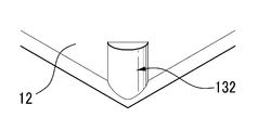
도 4는 도 1에 도시한 유기 발광 표시 장치 중 표시 패널의 평면도이고, 도 5는 도 4의 부분 확대도이다.FIG. 4 is a plan view of a display panel of the organic light emitting display device shown in FIG. 1, and FIG. 5 is a partially enlarged view of FIG.
도 4와 도 5를 참고하면, 제2 기판(12)은 4개의 직각 코너 중 적어도 하나의 코너에 접착 물질의 흐름을 유도하는 채널(13)을 형성한다. 도 4에서는 제2 기판(12)이 4개의 직각 코너 모두에 채널(13)을 형성한 경우를 예로 들어 도시하였다.Referring to Figures 4 and 5, the
채널(13)은 제2 기판(12)의 외면에 형성된 오목 홈으로 이루어지며, 제2 기판(12)의 코너에서 대각 방향을 따라 형성된다. 여기서 '대각 방향'은 제2 기판(12)의 장변 및 단변에 대해 소정의 각도를 갖는 방향으로 정의된다. 예를 들어, 채널(13)은 제2 기판(12)의 장변 및 단변에 대해 45도의 경사각을 가질 수 있다. 채널(13)의 경사각은 45도로 한정되지 않으며, 접착 물질의 퍼짐 형태에 따라 다양하게 설정될 수 있다.The
채널(13)은 일정한 폭과 소정의 길이를 가진 단일 막대형으로 이루어지며, 사각의 단면 형상을 가질 수 있다. 이 경우 채널(13)은 평평한 바닥부(13a)와, 복수의 수직 측벽(13b)으로 구성된다. 채널(13)은 제2 기판(12)의 코너 모서리와 접하도록 형성된다. 따라서 채널(13)은 전체적으로 사각 막대형으로 이루어지나 채널(13)의 단부는 코너 모서리에 대응하는 직각 형태를 가진다.The
채널(13)은 표시 영역(A10)을 침범하지 않도록 표시 영역(A10)의 외측에 위치한다. 즉 채널(13)은 제2 기판(12) 중 커버 윈도우(30)의 차광부(31)에 대응하는 위치에 형성되며, 채널(13)로 인한 제2 기판(12)의 단차가 이미지 표시에 영향을 미치지 않도록 한다.The
전술한 구성의 채널(13)은 제2 기판(12) 또는 커버 윈도우(30)의 중앙부에 도포된 접착 물질이 표시 패널(10)과 커버 윈도우(30)의 적층 압력에 의해 넓게 퍼질 때 채널(13)의 길이 방향을 따라 접착 물질의 흐름을 유도하여 접착 물질의 퍼짐성을 높이는 역할을 한다. 따라서 접착층(20)은 채널(13)을 포함한 제2 기판(12)의 모서리 상부를 채운다.The
이와 같이 제2 기판(12)의 코너에 채널(13)이 형성됨에 따라, 제2 기판(12)의 코너에서 접착층(20)이 차지하는 면적이 확대되고, 접착층(20)이 제2 기판(12)의 코너 모서리까지 치밀하게 형성될 수 있다. 그 결과, 제1 실시예의 유기 발광 표시 장치(100)는 표시 패널(10)과 커버 윈도우(30)의 접착 신뢰성을 높일 수 있다.As the
도 6 내지 도 8은 도 5에 도시한 채널의 여러 변형예를 나타낸 제2 기판의 부분 확대도이다.6 to 8 are partially enlarged views of a second substrate showing various modifications of the channel shown in Fig.
도 6을 참고하면, 채널(131)은 삼각의 단면 형상을 가질 수 있으며, 이 경우 2개의 경사면이 채널을 구성한다. 도 7을 참고하면, 채널(132)은 타원형 또는 반원형의 단면 형상을 가질 수 있다. 도 8을 참고하면, 채널(133)은 서로 나란한 복수의 미세 채널로 구성되며, 각각의 미세 채널은 삼각의 단면 형상을 가질 수 있다.Referring to FIG. 6, the
채널(13, 131, 132, 133)의 형상은 도시한 예들로 한정되지 않으며, 제2 기판(12)의 코너에 음각 형태로 구비되어 제2 기판(12)의 코너 모서리를 향해 접착 물질의 흐름을 유도할 수 있는 형상이면 모두 적용 가능하다.The shapes of the
도 9는 본 발명의 제2 실시예에 따른 유기 발광 표시 장치 중 커버 윈도우의 내면과 표시 패널을 나타낸 개략도이다.9 is a schematic view showing an inner surface of a cover window and a display panel of an OLED display according to a second embodiment of the present invention.
도 9를 참고하면, 제2 실시예의 유기 발광 표시 장치는 채널(134a, 134b)이 제2 기판(12) 대신 커버 윈도우(30)의 내면에 형성된 것을 제외하고 전술한 제1 실시예의 유기 발광 표시 장치와 동일한 구성으로 이루어진다. 제1 실시예와 같은 부재에 대해서는 같은 도면 부호를 사용하며, 아래에서는 제1 실시예와 다른 구성에 대해 주로 설명한다.9, except that the
커버 윈도우(30)는 4개의 직각 코너를 가지는데 이 중 2개의 직각 코너는 제2 기판(12)의 직각 코너와 마주하고, 다른 2개의 직각 코너는 제1 기판(11)의 직각 코너와 마주한다. 커버 윈도우(30)는 제2 기판(12)의 직각 코너와 마주하는 2개의 직각 코너에 채널(134a)을 형성할 수 있다. 또한, 커버 윈도우(30)는 패드 영역(A20)과 접하는 제2 기판(12)의 직각 코너와 마주하는 위치에 채널(134b)을 형성할 수 있다.The
커버 윈도우(30)에 형성된 채널(134a, 134b) 또한 대각 방향을 따라 형성되며, 일정한 폭과 소정의 길이를 가진 단일 막대형으로서 사각, 삼각, 타원, 또는 반원형의 단면 형상을 가질 수 있다. 다른 한편으로, 채널(134a, 134b)은 서로 나란한 복수의 미세 채널로 구성될 수 있다. 도 9에서는 단일 막대형 채널을 예로 들어 도시하였다. 커버 윈도우(30)에 형성된 채널(134a, 134b)은 표시 영역(A10)을 침범하지 않도록 표시 영역(A10)의 외측, 즉 차광부(31)에 위치한다.
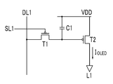
도 10은 도 1에 도시한 표시 패널의 화소 회로를 나타낸 배치도이고, 도 11은 도 1에 도시한 표시 패널의 부분 확대 단면도이다.Fig. 10 is a layout diagram showing the pixel circuit of the display panel shown in Fig. 1, and Fig. 11 is a partially enlarged cross-sectional view of the display panel shown in Fig.
도 10과 도 11을 참고하면, 화소는 유기 발광 다이오드(L1)와 구동 회로부(T1, T2, C1)를 포함한다. 유기 발광 다이오드(L1)는 화소 전극(141)과 유기 발광층(142) 및 공통 전극(143)을 포함한다. 구동 회로부(T1, T2, C1)는 적어도 2개의 박막 트랜지스터(스위칭 트랜지스터(T1) 및 구동 트랜지스터(T2))와 적어도 하나의 캐패시터(C1)를 포함한다.Referring to FIGS. 10 and 11, the pixel includes an organic light emitting diode (LED) L1 and driving circuit portions T1, T2, and C1. The organic light emitting diode L 1 includes a
스위칭 트랜지스터(T2)는 스캔 라인(SL1)과 데이터 라인(DL1)에 연결되고, 스캔 라인(SL1)에 입력되는 스위칭 전압에 따라 데이터 라인(DL1)에서 입력되는 데이터 전압을 구동 트랜지스터(T2)로 전송한다. 캐패시터(C1)는 스위칭 트랜지스터(T1)와 전원 라인(VDD)에 연결되며, 스위칭 트랜지스터(T1)로부터 전송받은 전압과 전원 라인(VDD)에 공급되는 전압의 차이에 해당하는 전압을 저장한다.The switching transistor T2 is connected to the scan line SL1 and the data line DL1 and supplies a data voltage input from the data line DL1 to the driving transistor T2 according to a switching voltage input to the scan line SL1 send. The capacitor C1 is connected to the switching transistor T1 and the power supply line VDD and stores a voltage corresponding to a difference between a voltage received from the switching transistor T1 and a voltage supplied to the power supply line VDD.
구동 트랜지스터(T2)는 전원 라인(VDD)과 캐패시터(C1)에 연결되어 캐패시터(C1)에 저장된 전압과 문턱 전압의 차이의 제곱에 비례하는 출력 전류(IOLED)를 유기 발광 다이오드(L1)로 공급하고, 유기 발광 다이오드(L1)는 출력 전류(IOLED)에 비례하는 세기로 발광한다. 구동 트랜지스터(T2)는 게이트 전극(181)과 소스/드레인 전극(182, 183)을 포함하며, 화소 전극(141)은 구동 트랜지스터(T2)의 드레인 전극(183)에 연결될 수 있다.A driving transistor (T2) is a power supply line (VDD) and the output current (I OLED) in proportion to the stored voltage and the square of the difference of the threshold voltage on the capacitor (C1) is connected to the capacitor (C1) to the organic light emitting diode (L1) And the organic light emitting diode L1 emits light with an intensity proportional to the output current I OLED . The driving transistor T2 may include a
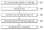
도 12는 본 발명의 일 실시예에 따른 유기 발광 표시 장치의 제조 방법을 나타낸 공정 순서도이다.FIG. 12 is a flowchart illustrating a method of manufacturing an organic light emitting display according to an embodiment of the present invention. Referring to FIG.
도 12를 참고하면, 유기 발광 표시 장치의 제조 방법은, 표시 영역과 패드 영역을 구비한 제1 기판 및 표시 영역을 덮는 제2 기판을 구비한 표시 패널을 제공하는 제1 단계(S10)와, 커버 윈도우를 제공하는 제2 단계(S20)와, 커버 윈도우 또는 제2 기판에 접착 물질을 도포하는 제3 단계(S30)를 포함한다. 또한, 유기 발광 표시 장치의 제조 방법은 커버 윈도우의 내면이 제2 기판과 마주하도록 제2 기판 상에 커버 윈도우를 배치하고, 커버 윈도우에 압력을 가하여 접착 물질을 넓게 퍼트리는 제4 단계(S40)와, 접착 물질을 경화시켜 접착층을 형성하는 제5 단계(S50)를 포함한다.12, a method of manufacturing an organic light emitting display includes a first step (S10) of providing a display panel including a first substrate having a display region and a pad region and a second substrate covering the display region, A second step (S20) of providing a cover window, and a third step (S30) of applying an adhesive material to the cover window or the second substrate. The method further includes a fourth step (S40) of disposing a cover window on the second substrate so that the inner surface of the cover window faces the second substrate, and applying pressure to the cover window to spread the adhesive material, And a fifth step (S50) of curing the adhesive material to form an adhesive layer.
도 13은 도 12에 도시한 제3 단계의 커버 윈도우를 나타낸 평면도이다.13 is a plan view showing a cover window of the third step shown in Fig.
도 13을 참고하면, 제3 단계(S30)에서 접착 물질(25)은 액상 또는 페이스트상의 형태로 커버 윈도우(30)의 투광부(32)에 도포된다. 접착 물질(25)은 자외선 또는 열에 의해 경화되는 아크릴계 수지를 포함할 수 있으며, 대략 2개의 Y를 상하 방향으로 붙인 모양으로 도포될 수 있다. 도 13에서는 접착 물질(25)이 커버 윈도우(30)의 내면에 도포된 경우를 예로 들어 도시하였으나, 접착 물질(25)은 제2 기판(12)의 외면에 도포될 수도 있다.Referring to FIG. 13, in the third step S30, the
도 14와 도 15는 도 12에 도시한 제4 단계의 유기 발광 표시 장치를 나타낸 단면도이다.FIGS. 14 and 15 are cross-sectional views illustrating the organic light emitting display device of the fourth step shown in FIG.
도 14와 도 15를 참고하면, 제4 단계(S40)에서 접착 물질(25)은 제2 기판(12)과 커버 윈도우(30)의 적층 압력에 의해 사방으로 넓게 퍼진다. 이때 제2 기판(12)의 코너에 오목한 채널(13)이 형성되어 있으므로, 제2 기판(12)의 코너를 향해 확산되는 접착 물질(25)은 채널(13)의 길이 방향을 따라 그 흐름이 보다 쉽게 이루어진다.14 and 15, in the fourth step S40, the
따라서 접착 물질(25)은 채널(13)을 타고 제2 기판(12)의 코너 모서리까지 쉽게 도달하며, 제2 기판(12)의 코너 모서리 전체를 치밀하게 채울 수 있다. 도 14와 도 15에서는 채널(13)이 제2 기판(12)의 코너에 형성된 경우를 예로 들어 도시하였으나, 채널(13)은 커버 윈도우(30)의 내면에 형성될 수도 있다.Thus, the
이와 같이 제2 기판(12) 또는 커버 윈도우(30)에 채널(13)을 형성함에 따라, 본 실시예의 유기 발광 표시 장치(100)는 제2 기판(12)의 코너에서 접착층(20)이 차지하는 면적을 늘리며, 접착층(20)이 제2 기판(12)의 코너를 전부 채우지 못하는 미도포 불량을 방지할 수 있다. 그 결과, 코너측에서 표시 패널(10)과 커버 윈도우(30)가 들뜨는 불량이 발생하지 않으며, 표시 패널(10)과 커버 윈도우(30)의 접착 신뢰성을 높일 수 있다.As the
상기에서는 본 발명의 바람직한 실시예에 대하여 설명하였지만, 본 발명은 이에 한정되는 것이 아니고 특허청구범위와 발명의 상세한 설명 및 첨부한 도면의 범위 안에서 여러 가지로 변형하여 실시하는 것이 가능하고 이 또한 본 발명의 범위에 속하는 것은 당연하다.While the present invention has been described in connection with what is presently considered to be practical exemplary embodiments, it is to be understood that the invention is not limited to the disclosed embodiments, but, on the contrary, Of course.
100: 유기 발광 표시 장치 10: 표시 패널
11: 제1 기판 12: 제2 기판
A10: 표시 영역 A20: 패드 영역
13, 131, 132, 133, 134a, 134b: 채널
20: 접착층 25: 접착 물질
30: 커버 윈도우 31: 차광부
32: 투광부 40: 회로 필름
50: 인쇄 회로 기판100: organic light emitting display device 10: display panel
11: first substrate 12: second substrate
A10: display area A20: pad area
13, 131, 132, 133, 134a, 134b:
20: adhesive layer 25: adhesive material
30: cover window 31: light shield
32: transparent portion 40: circuit film
50: printed circuit board
Claims (14)
상기 표시 패널의 표시면 외측에 위치하는 커버 윈도우; 및
상기 표시면과 상기 커버 윈도우 사이에 위치하는 접착층
을 포함하며,
상기 표시 패널과 상기 커버 윈도우 중 어느 하나는 적어도 하나의 코너에 오목한 채널을 형성하고,
상기 접착층은 상기 채널을 채우는 유기 발광 표시 장치.A display panel for displaying an image;
A cover window located outside the display surface of the display panel; And
The adhesive layer located between the display surface and the cover window
/ RTI >
Wherein one of the display panel and the cover window forms a concave channel in at least one corner,
Wherein the adhesive layer fills the channel.
상기 표시 패널은,
표시 영역과 패드 영역을 구비한 제1 기판; 및
상기 표시 영역을 덮도록 상기 제1 기판에 부착된 제2 기판
을 포함하며,
상기 표시면은 상기 제2 기판의 외면인 유기 발광 표시 장치.The method according to claim 1,
In the display panel,
A first substrate having a display region and a pad region; And
A second substrate attached to the first substrate so as to cover the display area,
/ RTI >
Wherein the display surface is an outer surface of the second substrate.
상기 제2 기판은 4개의 직각 코너를 가지며,
상기 채널은 상기 4개의 직각 코너 중 적어도 한 곳에 형성되는 유기 발광 표시 장치.3. The method of claim 2,
The second substrate has four right-angled corners,
Wherein the channel is formed in at least one of the four right-angled corners.
상기 채널은 상기 제2 기판의 코너에서 대각 방향을 따라 형성되고, 상기 코너의 모서리와 접하며, 상기 표시 영역의 외측에 위치하는 유기 발광 표시 장치.The method of claim 3,
Wherein the channel is formed along a diagonal direction at a corner of the second substrate, is in contact with a corner of the corner, and is located outside the display region.
상기 채널은 단일 막대형으로 형성되고, 사각, 삼각, 타원형, 또는 반원형 중 어느 하나의 단면 형상을 가지는 유기 발광 표시 장치.The method of claim 3,
Wherein the channel is formed into a single film and has a cross-sectional shape of any one of a square, a triangle, an ellipse, or a semicircle.
상기 채널은 서로 나란한 복수의 미세 채널로 구성되고,
상기 복수의 미세 채널 각각은 삼각의 단면 형상을 가지는 유기 발광 표시 장치.The method of claim 3,
Wherein the channel is composed of a plurality of microchannels arranged side by side,
Wherein each of the plurality of microchannels has a triangular cross-sectional shape.
상기 커버 윈도우는 상기 제2 기판과 상기 패드 영역을 커버하며, 상기 패드 영역을 포함한 상기 표시 패널의 가장자리에 대응하는 차광부 및 상기 표시 영역에 대응하는 투광부를 포함하는 유기 발광 표시 장치.3. The method of claim 2,
Wherein the cover window covers the second substrate and the pad region, and includes a light-shielding portion corresponding to an edge of the display panel including the pad region, and a translucent portion corresponding to the display region.
상기 제2 기판은 4개의 직각 코너를 가지며,
상기 채널은 상기 커버 윈도우의 내면에서 상기 4개의 직각 코너 중 적어도 하나의 코너와 마주하는 위치에 형성되는 유기 발광 표시 장치.8. The method of claim 7,
The second substrate has four right-angled corners,
Wherein the channel is formed at a position facing the corner of at least one of the four right-angled corners on the inner surface of the cover window.
상기 채널은 대각 방향을 따라 형성되고, 상기 차광부에 위치하는 유기 발광 표시 장치.9. The method of claim 8,
Wherein the channel is formed along a diagonal direction and is located in the light-shielding portion.
상기 채널은 단일 막대형으로 형성되고, 사각, 삼각, 타원형, 또는 반원형 중 어느 하나의 단면 형상을 가지는 유기 발광 표시 장치.9. The method of claim 8,
Wherein the channel is formed into a single film and has a cross-sectional shape of any one of a square, a triangle, an ellipse, or a semicircle.
상기 채널은 서로 나란한 복수의 미세 채널로 구성되고,
상기 복수의 미세 채널 각각은 삼각의 단면 형상을 가지는 유기 발광 표시 장치.9. The method of claim 8,
Wherein the channel is composed of a plurality of microchannels arranged side by side,
Wherein each of the plurality of microchannels has a triangular cross-sectional shape.
커버 윈도우를 제공하는 단계;
상기 커버 윈도우 또는 상기 제2 기판 상에 접착 물질을 도포하는 단계;
상기 제2 기판 상에 상기 커버 윈도우를 배치하고, 상기 커버 윈도우에 압력을 가하여 상기 접착 물질을 넓게 퍼트리는 단계; 및
상기 접착 물질을 경화시켜 접착층을 형성하는 단계
를 포함하며,
상기 제2 기판과 상기 커버 윈도우 중 어느 하나의 코너에 오목한 채널이 형성되고, 상기 접착 물질을 퍼트리는 단계에서 상기 접착 물질이 상기 채널을 타고 상기 제2 기판의 코너 모서리를 향해 이동하는 유기 발광 표시 장치의 제조 방법.Providing a display panel including a first substrate having a display area and a pad area, and a second substrate covering the display area;
Providing a cover window;
Applying an adhesive material on the cover window or the second substrate;
Disposing the cover window on the second substrate and applying pressure to the cover window to broaden the adhesive material; And
And curing the adhesive material to form an adhesive layer
/ RTI >
Wherein a concave channel is formed at a corner of one of the second substrate and the cover window and the adhesive material moves toward the corner of the second substrate on the channel in the step of spreading the adhesive material, ≪ / RTI >
상기 접착 물질은 아크릴계 수지를 포함하며, 자외선 또는 열에 의해 경화되어 상기 접착층을 형성하는 유기 발광 표시 장치의 제조 방법.13. The method of claim 12,
Wherein the adhesive material comprises an acrylic resin and is cured by ultraviolet rays or heat to form the adhesive layer.
상기 접착 물질은 상기 채널을 포함한 상기 제2 기판과 상기 커버 윈도우 사이의 공간을 채워 상기 접착층을 형성하는 유기 발광 표시 장치의 제조 방법.13. The method of claim 12,
Wherein the adhesive material fills a space between the second substrate including the channel and the cover window to form the adhesive layer.
Priority Applications (2)
| Application Number | Priority Date | Filing Date | Title |
|---|---|---|---|
| KR1020120120457A KR20140056548A (en) | 2012-10-29 | 2012-10-29 | Organic light emitting diode display and manufacturing method thereof |
| US13/828,434 US9626897B2 (en) | 2012-10-29 | 2013-03-14 | Organic light emitting diode display device and method of manufacturing the same |
Applications Claiming Priority (1)
| Application Number | Priority Date | Filing Date | Title |
|---|---|---|---|
| KR1020120120457A KR20140056548A (en) | 2012-10-29 | 2012-10-29 | Organic light emitting diode display and manufacturing method thereof |
Publications (1)
| Publication Number | Publication Date |
|---|---|
| KR20140056548A true KR20140056548A (en) | 2014-05-12 |
Family
ID=50546597
Family Applications (1)
| Application Number | Title | Priority Date | Filing Date |
|---|---|---|---|
| KR1020120120457A KR20140056548A (en) | 2012-10-29 | 2012-10-29 | Organic light emitting diode display and manufacturing method thereof |
Country Status (2)
| Country | Link |
|---|---|
| US (1) | US9626897B2 (en) |
| KR (1) | KR20140056548A (en) |
Cited By (4)
| Publication number | Priority date | Publication date | Assignee | Title |
|---|---|---|---|---|
| KR20160124289A (en) * | 2015-04-16 | 2016-10-27 | 삼성디스플레이 주식회사 | Display device |
| KR20180081191A (en) * | 2017-01-05 | 2018-07-16 | 삼성디스플레이 주식회사 | Display apparatus |
| US10854851B2 (en) | 2018-01-02 | 2020-12-01 | Samsung Display Co., Ltd. | Display device |
| US11785835B2 (en) | 2014-10-28 | 2023-10-10 | Semiconductor Energy Laboratory Co., Ltd. | Touch panel having a photoelectric conversion element between the first and second flexible substrates |
Families Citing this family (3)
| Publication number | Priority date | Publication date | Assignee | Title |
|---|---|---|---|---|
| CN104709714B (en) * | 2015-02-28 | 2017-06-30 | 京东方科技集团股份有限公司 | The conveyer and method of display panel |
| KR102552930B1 (en) * | 2018-06-27 | 2023-07-07 | 삼성디스플레이 주식회사 | Panel bottom member and display device including the same |
| WO2021176955A1 (en) * | 2020-03-05 | 2021-09-10 | パイオニア株式会社 | Light-emitting device and sealing part |
Family Cites Families (12)
| Publication number | Priority date | Publication date | Assignee | Title |
|---|---|---|---|---|
| TW518910B (en) * | 2000-12-20 | 2003-01-21 | Koninkl Philips Electronics Nv | Device, particularly an electroluminescent display device, and method of manufacturing such a device |
| US6892578B2 (en) * | 2002-11-29 | 2005-05-17 | Hitachi Metals Ltd. | Acceleration sensor |
| JP2007035536A (en) * | 2005-07-29 | 2007-02-08 | Rohm Co Ltd | Flat panel display |
| KR100798632B1 (en) | 2006-12-30 | 2008-01-28 | 주식회사 모젬 | Window for display device and wireless terminal unit comprising the same |
| KR100953654B1 (en) * | 2008-06-26 | 2010-04-20 | 삼성모바일디스플레이주식회사 | Organic light emitting diode display and method for manufacturing the smae |
| KR101117399B1 (en) | 2010-05-11 | 2012-03-07 | 주식회사 에이치엔에이치글로벌리소스 | Portable display device and method for assembling the same |
| KR20120004862A (en) | 2010-07-07 | 2012-01-13 | 삼성모바일디스플레이주식회사 | Organic light emitting diode display |
| KR20120044041A (en) | 2010-10-27 | 2012-05-07 | 삼성모바일디스플레이주식회사 | Display device |
| KR20120044501A (en) | 2010-10-28 | 2012-05-08 | 삼성모바일디스플레이주식회사 | Display device having a touch screen panel and manufacturing method of the same |
| KR101752442B1 (en) | 2010-12-14 | 2017-07-04 | 삼성디스플레이 주식회사 | Flat panel display |
| KR20120091871A (en) | 2011-02-10 | 2012-08-20 | 삼성디스플레이 주식회사 | Display device and method for manufacturing the same |
| KR101835109B1 (en) | 2011-05-30 | 2018-03-07 | 삼성디스플레이 주식회사 | flat display device |
-
2012
- 2012-10-29 KR KR1020120120457A patent/KR20140056548A/en not_active Application Discontinuation
-
2013
- 2013-03-14 US US13/828,434 patent/US9626897B2/en active Active
Cited By (4)
| Publication number | Priority date | Publication date | Assignee | Title |
|---|---|---|---|---|
| US11785835B2 (en) | 2014-10-28 | 2023-10-10 | Semiconductor Energy Laboratory Co., Ltd. | Touch panel having a photoelectric conversion element between the first and second flexible substrates |
| KR20160124289A (en) * | 2015-04-16 | 2016-10-27 | 삼성디스플레이 주식회사 | Display device |
| KR20180081191A (en) * | 2017-01-05 | 2018-07-16 | 삼성디스플레이 주식회사 | Display apparatus |
| US10854851B2 (en) | 2018-01-02 | 2020-12-01 | Samsung Display Co., Ltd. | Display device |
Also Published As
| Publication number | Publication date |
|---|---|
| US20140118230A1 (en) | 2014-05-01 |
| US9626897B2 (en) | 2017-04-18 |
Similar Documents
| Publication | Publication Date | Title |
|---|---|---|
| GB2542503B (en) | Display device | |
| CN110783361B (en) | Display device, backlight module and electronic device | |
| KR20140056548A (en) | Organic light emitting diode display and manufacturing method thereof | |
| KR100953654B1 (en) | Organic light emitting diode display and method for manufacturing the smae | |
| KR102045244B1 (en) | Flexible display device | |
| US20160349565A1 (en) | Narrow bezel display device | |
| KR101984245B1 (en) | Organic light emitting diode display | |
| KR102048467B1 (en) | Organic light emitting diode display device | |
| KR101872084B1 (en) | Display device | |
| KR20210036444A (en) | Display device | |
| CN110416393B (en) | Electronic device | |
| US9111889B2 (en) | Display device | |
| KR101811341B1 (en) | Organic light emitting diode display | |
| US9761835B2 (en) | Display device | |
| KR20170026755A (en) | Display apparatus | |
| KR102122599B1 (en) | Organic light emitting display | |
| KR20200145268A (en) | Electroluminescence Display Having Micro-Lens Layer | |
| KR100759758B1 (en) | Display device and manufacturing method therof | |
| KR20210091856A (en) | Display device and method of fabricating the same | |
| KR20170071282A (en) | Organic light emitting display device | |
| KR102427765B1 (en) | Display Panel and Display Device | |
| US20210132720A1 (en) | Display device | |
| KR20130081924A (en) | Organic light emitting diode display and manufacturing method thereof | |
| KR102162169B1 (en) | Display device and method of manufacturing the same | |
| KR102648611B1 (en) | Display device having jointing auxiliary member |
Legal Events
| Date | Code | Title | Description |
|---|---|---|---|
| WITN | Application deemed withdrawn, e.g. because no request for examination was filed or no examination fee was paid |