KR20140031215A - System and method of updating drive scheme voltages - Google Patents
System and method of updating drive scheme voltages Download PDFInfo
- Publication number
- KR20140031215A KR20140031215A KR1020137027201A KR20137027201A KR20140031215A KR 20140031215 A KR20140031215 A KR 20140031215A KR 1020137027201 A KR1020137027201 A KR 1020137027201A KR 20137027201 A KR20137027201 A KR 20137027201A KR 20140031215 A KR20140031215 A KR 20140031215A
- Authority
- KR
- South Korea
- Prior art keywords
- voltage
- display elements
- subset
- array
- voltages
- Prior art date
Links
Images


Classifications
-
- G—PHYSICS
- G09—EDUCATION; CRYPTOGRAPHY; DISPLAY; ADVERTISING; SEALS
- G09G—ARRANGEMENTS OR CIRCUITS FOR CONTROL OF INDICATING DEVICES USING STATIC MEANS TO PRESENT VARIABLE INFORMATION
- G09G3/00—Control arrangements or circuits, of interest only in connection with visual indicators other than cathode-ray tubes
- G09G3/20—Control arrangements or circuits, of interest only in connection with visual indicators other than cathode-ray tubes for presentation of an assembly of a number of characters, e.g. a page, by composing the assembly by combination of individual elements arranged in a matrix no fixed position being assigned to or needed to be assigned to the individual characters or partial characters
- G09G3/34—Control arrangements or circuits, of interest only in connection with visual indicators other than cathode-ray tubes for presentation of an assembly of a number of characters, e.g. a page, by composing the assembly by combination of individual elements arranged in a matrix no fixed position being assigned to or needed to be assigned to the individual characters or partial characters by control of light from an independent source
- G09G3/3433—Control arrangements or circuits, of interest only in connection with visual indicators other than cathode-ray tubes for presentation of an assembly of a number of characters, e.g. a page, by composing the assembly by combination of individual elements arranged in a matrix no fixed position being assigned to or needed to be assigned to the individual characters or partial characters by control of light from an independent source using light modulating elements actuated by an electric field and being other than liquid crystal devices and electrochromic devices
- G09G3/3466—Control arrangements or circuits, of interest only in connection with visual indicators other than cathode-ray tubes for presentation of an assembly of a number of characters, e.g. a page, by composing the assembly by combination of individual elements arranged in a matrix no fixed position being assigned to or needed to be assigned to the individual characters or partial characters by control of light from an independent source using light modulating elements actuated by an electric field and being other than liquid crystal devices and electrochromic devices based on interferometric effect
-
- G—PHYSICS
- G09—EDUCATION; CRYPTOGRAPHY; DISPLAY; ADVERTISING; SEALS
- G09G—ARRANGEMENTS OR CIRCUITS FOR CONTROL OF INDICATING DEVICES USING STATIC MEANS TO PRESENT VARIABLE INFORMATION
- G09G3/00—Control arrangements or circuits, of interest only in connection with visual indicators other than cathode-ray tubes
- G09G3/20—Control arrangements or circuits, of interest only in connection with visual indicators other than cathode-ray tubes for presentation of an assembly of a number of characters, e.g. a page, by composing the assembly by combination of individual elements arranged in a matrix no fixed position being assigned to or needed to be assigned to the individual characters or partial characters
- G09G3/34—Control arrangements or circuits, of interest only in connection with visual indicators other than cathode-ray tubes for presentation of an assembly of a number of characters, e.g. a page, by composing the assembly by combination of individual elements arranged in a matrix no fixed position being assigned to or needed to be assigned to the individual characters or partial characters by control of light from an independent source
- G09G3/36—Control arrangements or circuits, of interest only in connection with visual indicators other than cathode-ray tubes for presentation of an assembly of a number of characters, e.g. a page, by composing the assembly by combination of individual elements arranged in a matrix no fixed position being assigned to or needed to be assigned to the individual characters or partial characters by control of light from an independent source using liquid crystals
-
- G—PHYSICS
- G09—EDUCATION; CRYPTOGRAPHY; DISPLAY; ADVERTISING; SEALS
- G09G—ARRANGEMENTS OR CIRCUITS FOR CONTROL OF INDICATING DEVICES USING STATIC MEANS TO PRESENT VARIABLE INFORMATION
- G09G3/00—Control arrangements or circuits, of interest only in connection with visual indicators other than cathode-ray tubes
- G09G3/20—Control arrangements or circuits, of interest only in connection with visual indicators other than cathode-ray tubes for presentation of an assembly of a number of characters, e.g. a page, by composing the assembly by combination of individual elements arranged in a matrix no fixed position being assigned to or needed to be assigned to the individual characters or partial characters
- G09G3/34—Control arrangements or circuits, of interest only in connection with visual indicators other than cathode-ray tubes for presentation of an assembly of a number of characters, e.g. a page, by composing the assembly by combination of individual elements arranged in a matrix no fixed position being assigned to or needed to be assigned to the individual characters or partial characters by control of light from an independent source
- G09G3/3433—Control arrangements or circuits, of interest only in connection with visual indicators other than cathode-ray tubes for presentation of an assembly of a number of characters, e.g. a page, by composing the assembly by combination of individual elements arranged in a matrix no fixed position being assigned to or needed to be assigned to the individual characters or partial characters by control of light from an independent source using light modulating elements actuated by an electric field and being other than liquid crystal devices and electrochromic devices
-
- G—PHYSICS
- G09—EDUCATION; CRYPTOGRAPHY; DISPLAY; ADVERTISING; SEALS
- G09G—ARRANGEMENTS OR CIRCUITS FOR CONTROL OF INDICATING DEVICES USING STATIC MEANS TO PRESENT VARIABLE INFORMATION
- G09G2320/00—Control of display operating conditions
- G09G2320/06—Adjustment of display parameters
- G09G2320/0693—Calibration of display systems
-
- G—PHYSICS
- G09—EDUCATION; CRYPTOGRAPHY; DISPLAY; ADVERTISING; SEALS
- G09G—ARRANGEMENTS OR CIRCUITS FOR CONTROL OF INDICATING DEVICES USING STATIC MEANS TO PRESENT VARIABLE INFORMATION
- G09G3/00—Control arrangements or circuits, of interest only in connection with visual indicators other than cathode-ray tubes
- G09G3/20—Control arrangements or circuits, of interest only in connection with visual indicators other than cathode-ray tubes for presentation of an assembly of a number of characters, e.g. a page, by composing the assembly by combination of individual elements arranged in a matrix no fixed position being assigned to or needed to be assigned to the individual characters or partial characters
- G09G3/34—Control arrangements or circuits, of interest only in connection with visual indicators other than cathode-ray tubes for presentation of an assembly of a number of characters, e.g. a page, by composing the assembly by combination of individual elements arranged in a matrix no fixed position being assigned to or needed to be assigned to the individual characters or partial characters by control of light from an independent source
- G09G3/36—Control arrangements or circuits, of interest only in connection with visual indicators other than cathode-ray tubes for presentation of an assembly of a number of characters, e.g. a page, by composing the assembly by combination of individual elements arranged in a matrix no fixed position being assigned to or needed to be assigned to the individual characters or partial characters by control of light from an independent source using liquid crystals
- G09G3/3611—Control of matrices with row and column drivers
- G09G3/3622—Control of matrices with row and column drivers using a passive matrix
- G09G3/3629—Control of matrices with row and column drivers using a passive matrix using liquid crystals having memory effects, e.g. ferroelectric liquid crystals
-
- G—PHYSICS
- G09—EDUCATION; CRYPTOGRAPHY; DISPLAY; ADVERTISING; SEALS
- G09G—ARRANGEMENTS OR CIRCUITS FOR CONTROL OF INDICATING DEVICES USING STATIC MEANS TO PRESENT VARIABLE INFORMATION
- G09G3/00—Control arrangements or circuits, of interest only in connection with visual indicators other than cathode-ray tubes
- G09G3/20—Control arrangements or circuits, of interest only in connection with visual indicators other than cathode-ray tubes for presentation of an assembly of a number of characters, e.g. a page, by composing the assembly by combination of individual elements arranged in a matrix no fixed position being assigned to or needed to be assigned to the individual characters or partial characters
- G09G3/34—Control arrangements or circuits, of interest only in connection with visual indicators other than cathode-ray tubes for presentation of an assembly of a number of characters, e.g. a page, by composing the assembly by combination of individual elements arranged in a matrix no fixed position being assigned to or needed to be assigned to the individual characters or partial characters by control of light from an independent source
- G09G3/36—Control arrangements or circuits, of interest only in connection with visual indicators other than cathode-ray tubes for presentation of an assembly of a number of characters, e.g. a page, by composing the assembly by combination of individual elements arranged in a matrix no fixed position being assigned to or needed to be assigned to the individual characters or partial characters by control of light from an independent source using liquid crystals
- G09G3/3611—Control of matrices with row and column drivers
- G09G3/3648—Control of matrices with row and column drivers using an active matrix
- G09G3/3651—Control of matrices with row and column drivers using an active matrix using multistable liquid crystals, e.g. ferroelectric liquid crystals
Abstract
본 개시물은 디스플레이 어레이들을 조정하기 위해, 컴퓨터 저장 매체상에서 인코딩된 컴퓨터 프로그램들을 포함하는, 시스템들, 방법들 및 장치를 제공한다. 일 양태에서, 디스플레이 어레이를 조정하는 방법은 특정한 구동 응답 특징을 결정하는 단계 및 디스플레이 어레이에 대한 이미지 데이터의 업데이트들 사이에서 특정한 구동 방식 전압을 업데이트하는 단계를 포함한다.This disclosure provides systems, methods, and apparatus that include computer programs encoded on a computer storage medium to manipulate display arrays. In one aspect, a method of adjusting a display array includes determining a particular drive response characteristic and updating a particular drive scheme voltage between updates of image data for the display array.
Description
본 개시물은 구동 방식 전압들의 동적 선택에 관한 것이다.This disclosure relates to dynamic selection of drive scheme voltages.
전자기계 시스템들은 전기 및 기계적 엘리먼트들, 액추에이터들, 트랜스듀서들, 센서들, 광학 컴포넌트들(예를 들어, 미러들), 및 전자장치를 갖는 디바이스들을 포함한다. 전자기계 시스템들은 마이크로스케일 및 나노스케일을 포함하지만 이에 제한되지 않는 다양한 스케일들로 제조될 수 있다. 예를 들어, 마이크로전자기계 시스템(MEMS) 디바이스는 약 일 미크론 내지 수백 미크론 이상의 범위의 사이즈들을 갖는 구조들을 포함할 수 있다. 나노전자기계 시스템(NEMS) 디바이스들은 예를 들어, 수백 나노미터들보다 작은 사이즈들을 포함하는, 일 미크론보다 작은 사이즈들을 갖는 구조들을 포함할 수 있다. 전자기계 엘리먼트들은 증착, 에칭, 리소그래피, 및/또는 기판들 및/또는 증착된 재료층들의 일부를 에칭하거나 층들을 추가하는 다른 마이크로가공 공정들을 사용하여 생성되어 전기 및 전자기계 디바이스들을 형성할 수도 있다.Electromechanical systems include devices with electrical and mechanical elements, actuators, transducers, sensors, optical components (eg, mirrors), and electronics. Electromechanical systems can be manufactured in various scales, including but not limited to microscale and nanoscale. For example, a microelectromechanical systems (MEMS) device may include structures having sizes ranging from about one micron to several hundreds of microns or more. Nanoelectromechanical system (NEMS) devices may include structures having sizes less than one micron, including, for example, sizes less than several hundred nanometers. Electromechanical elements may be produced using deposition, etching, lithography, and / or other micromachining processes that etch or add layers of substrates and / or deposited material layers to form electromechanical devices. .
전자기계 시스템 디바이스 중 일 타입을 간섭계형 변조기(IMOD)라 칭한다. 본 명세서에서 사용되는 바와 같이, 용어, 간섭계형 변조기 또는 간섭계형 광 변조기는 광 간섭의 원리들을 사용하여 광을 선택적으로 흡수 및/또는 반사하는 디바이스를 지칭한다. 일부 구현들에서, 간섭계형 변조기는 한 쌍의 도전성 플레이트들을 포함할 수도 있고, 이들 중 하나 또는 양자는 전체적으로 또는 부분적으로 투과형 및/또는 반사형일 수도 있고, 적절한 전기 신호의 인가시에 상대적 모션을 할 수 있다. 구현에서, 하나의 플레이트가 기판상에 증착된 정지층을 포함할 수도 있고 다른 층은 에어 갭에 의해 정지층으로부터 분리된 반사형 멤브레인을 포함할 수도 있다. 다른 플레이트에 대한 하나의 플레이트의 위치는 간섭계형 변조기상에 입사된 광의 광 간섭을 변화시킬 수 있다. 간섭계형 변조기 디바이스들은 광범위한 애플리케이션들을 갖고 기존의 제품들을 개선시키고 신규 제품들, 특히, 디스플레이 능력들을 갖는 제품들을 제조하는데 사용되는 것으로 기대된다.One type of electromechanical system device is called an interferometric modulator (IMOD). As used herein, the term interferometric modulator or interferometric light modulator refers to a device that selectively absorbs and / or reflects light using the principles of optical interference. In some implementations, the interferometric modulator may include a pair of conductive plates, one or both of which may be wholly or partially transmissive and / or reflective and may perform relative motion upon application of a suitable electrical signal. Can be. In an implementation, one plate may include a stop layer deposited on a substrate and the other layer may include a reflective membrane separated from the stop layer by an air gap. The position of one plate relative to the other may change the optical interference of light incident on the interferometric modulator. Interferometric modulator devices are expected to be used to improve existing products with a wide range of applications and to make new products, especially products with display capabilities.
본 개시물의 시스템들, 방법들 및 디바이스들은 여러 혁신적인 양태들을 각각 갖고, 이 중 단 하나가 본 명세서에 개시된 바람직한 속성들에 단독으로 책임이 있는 것은 아니다.The systems, methods, and devices of the present disclosure each have several innovative aspects, only one of which is not solely responsible for the preferred attributes disclosed herein.
본 개시물에 기재된 발명 대상의 하나의 혁신적인 양태는 복수의 디스플레이 엘리먼트들을 포함하는 어레이에서 구동 방식 전압들을 조정하는 방법으로 구현될 수 있다. 이 방법은 어레이의 디스플레이 엘리먼트들의 제 1 서브세트에 대해, 본질적으로 제 1 서브세트에서의 모든 디스플레이 엘리먼트들로 하여금 해제 상태(released state)로부터 작동하게 하는 전압을 특징으로 하는 제 1 전압을 결정하는 단계를 포함할 수도 있다. 이 방법은 어레이의 디스플레이 엘리먼트들의 제 2 서브세트에 대해, 제 2 서브세트에서의 제 1 디스플레이 엘리먼트로 하여금 해제 상태로부터 작동하게 하지만 제 2 서브세트에서의 상당한 수의 다른 디스플레이 엘리먼트들로 하여금 해제 상태로부터 작동하게 하지 않는 전압을 특징으로 하는 제 2 전압을 결정하는 단계를 또한 포함할 수도 있다. 이 방법은 또한, 어레이의 디스플레이 엘리먼트들의 제 3 서브세트에 대해, 제 3 서브세트에서의 제 1 디스플레이 엘리먼트로 하여금 작동 상태로부터 해제하게 하지만 제 3 서브세트에서의 상당한 수의 다른 디스플레이 엘리먼트들로 하여금 작동 상태로부터 해제하게 하지 않는 전압을 특징으로 하는 제 3 전압을 결정하는 단계를 또한 포함할 수도 있다. 또한, 이 방법은 어레이의 수명의 적어도 일부분에 걸친 어레이의 사용 동안 메인터넌스 조정들을 수행하기 위해 제 1, 제 2, 및 제 3 전압들을 사용하는 단계를 포함할 수도 있다. 일부 양태들에서, 적어도 하나의 구동 방식 전압이 제 1 전압, 제 2 전압, 및 제 3 전압에 적어도 부분적으로 기초하여 결정될 수도 있다. 일부 양태들에서, 메인터넌스 조정들을 수행하기 위해 제1, 제 2, 및 제 3 전압들을 사용하는 단계는 제 1, 제 2, 및 제 3 전압들을 반복적으로 결정하는 단계, 및 디스플레이의 수명에 걸쳐 주기적 간격으로 결정된 제 1, 제 2, 및 제 3 전압들에 기초하여 구동 방식 전압들을 업데이트하는 단계를 포함한다.One innovative aspect of the subject matter described in this disclosure can be implemented as a method of adjusting driving scheme voltages in an array comprising a plurality of display elements. The method determines for the first subset of display elements of the array a first voltage that is characterized by a voltage that essentially causes all display elements in the first subset to operate from a released state. It may also include a step. This method causes, for the second subset of display elements of the array, the first display element in the second subset to operate from the released state but a significant number of other display elements in the second subset cause the released state. The method may also include determining a second voltage characterized by a voltage that does not cause it to operate from. The method also causes, for the third subset of display elements of the array, to cause the first display element in the third subset to be released from the operating state but a significant number of other display elements in the third subset. It may also include determining a third voltage that is characterized by a voltage that does not cause it to release from the operating state. The method may also include using the first, second, and third voltages to perform maintenance adjustments during use of the array over at least a portion of the lifetime of the array. In some aspects, at least one drive scheme voltage may be determined based at least in part on the first voltage, the second voltage, and the third voltage. In some aspects, using the first, second, and third voltages to perform maintenance adjustments includes repeatedly determining the first, second, and third voltages, and periodically over the lifetime of the display. Updating the driving scheme voltages based on the first, second, and third voltages determined at intervals.
다른 양태에서, 복수의 디스플레이 엘리먼트들을 포함하는 어레이에서 구동 방식 전압들을 조정하는 방법은, 어레이의 디스플레이 엘리먼트들의 하나 또는 그 초과의 이전에 특징화된 서브세트들의 하나 또는 그 초과의 구동 응답 특징들을 결정하는 단계, 디스플레이 엘리먼트들의 하나 또는 그 초과의 이전에 특징화된 서브세트들에 대해 결정된 상기 결정된 구동 응답 특징들을 사용하여 구동 방식 전압들을 유도하는 단계, 및 어레이의 디스플레이 엘리먼트들의 추가의 상이한 서브세트를 특징화하기 위해 어레이의 디스플레이 엘리먼트들의 추가의 상이한 서브세트의 하나 또는 그 초과의 구동 응답 특징들을 결정하는 단계를 포함할 수도 있다. 일부 양태들에서, 어레이의 디스플레이 엘리먼트들의 추가의 상이한 서브세트는 어레이의 디스플레이 엘리먼트들의 하나 또는 그 초과의 이전에 특징화된 서브세트들 중 하나를 대체할 수도 있다.In another aspect, a method of adjusting driving scheme voltages in an array comprising a plurality of display elements determines one or more drive response characteristics of one or more previously characterized subsets of display elements of the array. Deriving drive scheme voltages using the determined drive response characteristics determined for one or more previously characterized subsets of display elements, and a further different subset of display elements of the array. Determining one or more drive response characteristics of a further different subset of display elements of the array to characterize. In some aspects, a further different subset of display elements of the array may replace one of one or more previously characterized subsets of display elements of the array.
다른 혁신적인 양태들이 구동 방식 전압들을 조정하는 장치에서 구현될 수도 있다. 이 장치는 디스플레이 엘리먼트들의 어레이, 디스플레이 엘리먼트 상태 감지 회로, 및 드라이버 및 프로세서 회로를 포함할 수도 있다. 드라이버 및 프로세서 회로는, 어레이의 디스플레이 엘리먼트들의 제 1 서브세트에 대해, 본질적으로 제 1 서브세트에서의 모든 디스플레이 엘리먼트들로 하여금 해제 상태로부터 작동하게 하는 전압을 특징으로 하는 제 1 전압을 결정하고, 어레이의 디스플레이 엘리먼트들의 제 2 서브세트에 대해, 제 2 서브세트에서의 제 1 디스플레이 엘리먼트로 하여금 해제 상태로부터 작동하게 하지만 제 2 서브세트에서의 상당한 수의 다른 디스플레이 엘리먼트들로 하여금 해제 상태로부터 작동하게 하지 않는 전압을 특징으로 하는 제 2 전압을 결정하며, 어레이의 디스플레이 엘리먼트들의 제 3 서브세트에 대해, 제 3 서브세트에서의 제 1 디스플레이 엘리먼트로 하여금 작동 상태로부터 해제하게 하지만 제 3 서브세트에서의 상당한 수의 다른 디스플레이 엘리먼트들로 하여금 작동 상태로부터 해제하게 하지 않는 전압을 특징으로 하는 제 3 전압을 결정하도록 구성될 수도 있다. 드라이버 및 프로세서 회로는 어레이의 사용 동안 메인터넌스 조정들을 수행하기 위해 제 1, 제 2, 및 제 3 전압들을 사용하도록 더 구성될 수도 있다.Other innovative aspects may be implemented in an apparatus for adjusting drive scheme voltages. The apparatus may include an array of display elements, display element state sensing circuitry, and driver and processor circuitry. The driver and processor circuits determine, for the first subset of display elements of the array, essentially a first voltage characterized by a voltage that causes all display elements in the first subset to operate from a released state, For the second subset of display elements of the array, cause the first display element in the second subset to operate from the released state but allow a significant number of other display elements in the second subset to operate from the released state. Determine a second voltage characterized by a voltage that does not, and for a third subset of display elements of the array, cause the first display element in the third subset to release from the operating state but not in the third subset. A considerable number of other display Ellie Causing teudeul may be configured to determine a third voltage, it characterized in that the voltage is not released from the operating state. The driver and processor circuit may be further configured to use the first, second, and third voltages to perform maintenance adjustments during use of the array.
다른 혁신적인 양태들이 구동 방식 전압들을 조정하는 장치에서 구현될 수도 있다. 이러한 양태에서, 장치는 디스플레이 엘리먼트들의 어레이, 디스플레이 엘리먼트 상태 감지 회로, 및 어레이의 디스플레이 엘리먼트들의 하나 또는 그 초과의 이전에 특징화된 서브세트들의 하나 또는 그 초과의 구동 응답 특징들을 결정하고, 디스플레이 엘리먼트들의 하나 또는 그 초과의 이전에 특징화된 서브세트들에 대해 결정된 상기 결정된 구동 응답 특징들을 사용하여 구동 방식 전압들을 유도하며, 어레이의 디스플레이 엘리먼트들의 추가의 상이한 서브세트를 특징화하기 위해 어레이의 디스플레이 엘리먼트들의 추가의 상이한 서브세트의 하나 또는 그 초과의 구동 응답 특징들을 결정하도록 구성된 드라이버 및 프로세서 회로를 포함할 수도 있다. Other innovative aspects may be implemented in an apparatus for adjusting drive scheme voltages. In this aspect, the apparatus determines one or more drive response characteristics of an array of display elements, display element state sensing circuitry, and one or more previously characterized subsets of display elements of the array, Display the array's display to characterize further different subsets of display elements of the array, using the determined drive response characteristics determined for one or more previously characterized subsets of It may include a driver and processor circuit configured to determine one or more drive response characteristics of a further different subset of elements.
다른 혁신적인 양태에서, 구동 방식 전압들을 조정하는 장치는 디스플레이 엘리먼트들의 어레이, 어레이의 디스플레이 엘리먼트들의 제 1 서브세트에 대해, 본질적으로 제 1 서브세트에서의 모든 디스플레이 엘리먼트들로 하여금 해제 상태로부터 작동하게 하는 전압을 특징으로 하는 제 1 전압을 결정하는 수단, 어레이의 디스플레이 엘리먼트들의 제 2 서브세트에 대해, 제 2 서브세트에서의 제 1 디스플레이 엘리먼트로 하여금 해제 상태로부터 작동하게 하지만 제 2 서브세트에서의 상당한 수의 다른 디스플레이 엘리먼트들로 하여금 해제 상태로부터 작동하게 하지 않는 전압을 특징으로 하는 제 2 전압을 결정하는 수단, 어레이의 디스플레이 엘리먼트들의 제 3 서브세트에 대해, 제 3 서브세트에서의 제 1 디스플레이 엘리먼트로 하여금 작동 상태로부터 해제하게 하지만 제 3 서브세트에서의 상당한 수의 다른 디스플레이 엘리먼트들로 하여금 작동 상태로부터 해제하게 하지 않는 전압을 특징으로 하는 제 3 전압을 결정하는 수단, 및 어레이의 사용 동안 메인터넌스 조정들을 수행하기 위해 제 1, 제 2, 및 제 3 전압들을 사용하는 수단을 포함한다. 일부 양태들에서, 제 1, 제 2, 및 제 3 전압들을 결정하는 수단은 적분기를 포함한다.In another innovative aspect, an apparatus for adjusting driving scheme voltages is configured for an array of display elements, a first subset of display elements of the array, to essentially cause all display elements in the first subset to operate from a released state. Means for determining a first voltage characterized by a voltage, for a second subset of display elements of the array, causing the first display element in the second subset to operate from a released state but with significant in the second subset Means for determining a second voltage characterized by a voltage that does not cause the number of other display elements to operate from a released state, for a third subset of display elements of the array, the first display element in the third subset Makes it work Means for determining a third voltage characterized by a voltage that causes the signal to be released but does not cause a significant number of other display elements in the third subset to be released from the operating state, and to perform maintenance adjustments during use of the array. Means for using the first, second, and third voltages. In some aspects, the means for determining the first, second, and third voltages includes an integrator.
다른 혁신적인 양태에서, 구동 방식 전압들을 조정하는 장치는, 디스플레이 엘리먼트들의 어레이, 어레이의 디스플레이 엘리먼트들의 하나 또는 그 초과의 이전에 특징화된 서브세트들의 하나 또는 그 초과의 구동 응답 특징들을 결정하는 수단, 디스플레이 엘리먼트들의 하나 또는 그 초과의 이전에 특징화된 서브세트들에 대해 결정된 상기 결정된 구동 응답 특징들을 사용하여 구동 방식 전압들을 유도하는 수단, 및 어레이의 디스플레이 엘리먼트들의 추가의 상이한 서브세트를 특징화하기 위해 어레이의 디스플레이 엘리먼트들의 추가의 상이한 서브세트의 하나 또는 그 초과의 구동 응답 특징들을 결정하는 수단을 포함한다. 일부 양태들에서, 장치는 어레이의 디스플레이 엘리먼트들의 하나 또는 그 초과의 이전에 특징화된 서브세트들 중 하나를 어레이의 디스플레이 엘리먼트들의 추가의 상이한 서브세트로 대체하는 수단을 더 포함할 수도 있다.In another innovative aspect, an apparatus for adjusting drive scheme voltages includes: an array of display elements, means for determining one or more drive response characteristics of one or more previously characterized subsets of display elements of the array, Means for deriving drive scheme voltages using the determined drive response characteristics determined for one or more previously characterized subsets of display elements, and characterizing a further different subset of display elements of the array. Means for determining one or more drive response characteristics of a further different subset of display elements of the array. In some aspects, the apparatus may further include means for replacing one of the one or more previously characterized subsets of display elements of the array with a further different subset of display elements of the array.
다른 혁신적인 양태에서, 비일시적 유형의 컴퓨터 판독가능 매체에는 드라이버 회로로 하여금, 어레이의 디스플레이 엘리먼트들의 제 1 서브세트에 대해, 본질적으로 제 1 서브세트에서의 모든 디스플레이 엘리먼트들로 하여금 해제 상태로부터 작동하게 하는 전압을 특징으로 하는 제 1 전압을 결정하는 단계, 어레이의 디스플레이 엘리먼트들의 제 2 서브세트에 대해, 제 2 서브세트에서의 제 1 디스플레이 엘리먼트로 하여금 해제 상태로부터 작동하게 하지만 제 2 서브세트에서의 상당한 수의 다른 디스플레이 엘리먼트들로 하여금 해제 상태로부터 작동하게 하지 않는 전압을 특징으로 하는 제 2 전압을 결정하는 단계, 어레이의 디스플레이 엘리먼트들의 제 3 서브세트에 대해, 제 3 서브세트에서의 제 1 디스플레이 엘리먼트로 하여금 작동 상태로부터 해제하게 하지만 제 3 서브세트에서의 상당한 수의 다른 디스플레이 엘리먼트들로 하여금 작동 상태로부터 해제하게 하지 않는 전압을 특징으로 하는 제 3 전압을 결정하는 단계, 및 어레이의 사용 동안 메인터넌스 조정들을 수행하기 위해 제 1, 제 2, 및 제 3 전압들을 사용하는 단계를 포함하는 방법을 수행하게 하는 명령어들이 저장된다.In another innovative aspect, a non-transitory type of computer readable medium includes driver circuitry to cause, for the first subset of display elements of the array, essentially all display elements in the first subset to operate from a released state. Determining a first voltage, characterized in that for a second subset of display elements of the array, causing the first display element in the second subset to operate from the released state but not in the second subset. Determining a second voltage characterized by a voltage that does not cause a significant number of other display elements to operate from a released state, for a third subset of display elements of the array, the first display in the third subset Allow the element to Determining a third voltage characterized by a voltage that causes release but does not cause a significant number of other display elements in the third subset to release from an operating state, and to perform maintenance adjustments during use of the array. Instructions are stored to perform a method comprising using the first, second, and third voltages.
다른 혁신적인 양태에서, 비일시적 유형의 컴퓨터 판독가능한 매체에는 드라이버 회로로 하여금, 어레이의 디스플레이 엘리먼트들의 하나 또는 그 초과의 이전에 특징화된 서브세트들의 하나 또는 그 초과의 구동 응답 특징들을 결정하는 단계, 디스플레이 엘리먼트들의 하나 또는 그 초과의 이전에 특징화된 서브세트들에 대해 결정된 상기 결정된 구동 응답 특징들을 사용하여 구동 방식 전압들을 유도하는 단계, 및 어레이의 디스플레이 엘리먼트들의 추가의 상이한 서브세트를 특징화하기 위해 어레이의 디스플레이 엘리먼트들의 추가의 상이한 서브세트의 하나 또는 그 초과의 구동 응답 특징들을 결정하는 단계를 포함하는 방법을 수행하게 하는 명령어들이 저장된다.In another innovative aspect, a non-transitory type of computer readable medium includes driver circuitry to determine one or more drive response characteristics of one or more previously characterized subsets of display elements of an array, Deriving drive scheme voltages using the determined drive response features determined for one or more previously characterized subsets of display elements, and characterizing a further different subset of display elements of the array. Instructions are stored that cause the method to perform the method comprising determining one or more drive response characteristics of a further different subset of display elements of the array.
본 명세서에 기재된 발명 대상의 하나 또는 그 초과의 구현들의 상세들이 첨부한 도면들 및 아래의 설명에 설명된다. 다른 특징들, 양태들, 및 이점들은 설명, 도면들, 및 청구항들로부터 명백해질 것이다. 아래의 도면들의 상대적 치수들은 일정한 비율로 도시되지 않을 수도 있다는 것에 유의한다.Details of one or more implementations of the subject matter described in this specification are set forth in the accompanying drawings and the description below. Other features, aspects, and advantages will become apparent from the description, drawings, and claims. It should be noted that the relative dimensions of the figures below may not be drawn to scale.
도 1은 간섭계형 변조기(IMOD) 디스플레이 디바이스의 일련의 디스플레이 엘리먼트들에서의 2개의 인접한 디스플레이 엘리먼트들을 도시하는 등축도의 일례를 도시한다.
도 2는 3×3 간섭계형 변조기 디스플레이를 통합한 전자 디바이스를 예시하는 시스템 블록도의 일례를 도시한다.
도 3은 도 1의 간섭계형 변조기에 대한 이동가능 반사층 위치 대 인가 전압을 예시하는 도면의 일례를 도시한다.
도 4는 다양한 공통 및 세그먼트 전압(common and segment voltage)들이 인가될 때 간섭계형 변조기의 다양한 상태들을 예시하는 테이블의 일례를 도시한다.
도 5a는 도 2의 3×3 간섭계형 변조기 디스플레이에서 디스플레이 데이터의 프레임을 예시하는 도면의 일례를 도시한다.
도 5b는 도 5a에 예시된 디스플레이 데이터의 프레임을 기록하기 위해 사용될 수도 있는 공통 및 세그먼트 신호들에 대한 타이밍도의 일례를 도시한다.
도 6a는 도 1의 간섭계형 변조기 디스플레이의 부분 단면의 일례를 도시한다.
도 6b 내지 도 6e는 간섭계형 변조기들의 변화하는 구현들의 단면들의 예들을 도시한다.
도 7은 간섭계형 변조기에 대한 제조 프로세스를 예시하는 흐름도의 일례를 도시한다.
도 8a 내지 도 8e는 간섭계형 변조기를 제조하는 방법에서의 다양한 스테이지들의 개략적인 단면도의 예들을 도시한다.
도 9는 픽셀 디스플레이 당 64 컬러의 구현을 구동시키는 공통 드라이버 및 세그먼트 드라이버의 예들을 예시하는 블록도이다.
도 10은 간섭계형 변조기들의 어레이의 여러 부재들에 대한 이동가능 반사 미러 위치 대 인가 전압을 예시하는 도면의 일례를 도시한다.
도 11은 간섭계형 변조기들의 어레이의 여러 부재들에 대한 이동가능 반사 미러 위치 대 인가 전압을 개념적으로 예시하는 도면의 다른 예를 도시한다.
도 12는 드라이버 회로 및 상태 감지 회로에 커플링된 디스플레이 어레이의 개략적인 블록도이다.
도 13은 도 12의 어레이에서 테스트 전하 흐름을 도시하는 개략도이다.
도 14a는 디스플레이 엘리먼트 응답 특징들을 검출하는 방법을 예시하는 플로우차트이다.
도 14b는 디스플레이 엘리먼트들의 라인에 대한 이력 곡선(hysteresis curve)을 정의하는 데이터 포인트들의 일례이다.
도 14c는 디스플레이 엘리먼트들의 라인에 대한 이력 곡선의 정규화된 제 1 도함수(derivative)의 추출의 일례이다.
도 14d는 도 14c의 정규화된 제 1 도함수 곡선으로부터 VAMAX _H 및 VAMIN _H를 선택하는 일례이다.
도 15는 어레이의 사용 동안 구동 방식 전압들을 조정하는 방법을 예시하는 플로우차트이다.
도 16은 구동 방식 전압 조정 루틴 동안 상태 감지를 위해 선택된 라인들의 일례를 예시한다.
도 17은 어레이의 사용 동안 구동 방식 전압들을 조정하는 방법을 예시하는 플로우차트이다.
도 18은 구동 방식 전압 조정 루틴 동안 상태 감지를 위해 선택된 라인들의 일례를 예시한다.
도 19a 및 도 19b는 복수의 간섭계형 변조기들을 포함하는 디스플레이 디바이스를 예시하는 시스템 블록도들의 예들을 도시한다.
다양한 도면들에서의 동일한 참조 부호들 및 지정들이 동일한 엘리먼트들을 나타낸다.1 shows an example of an isometric view showing two adjacent display elements in a series of display elements of an interferometric modulator (IMOD) display device.
2 shows an example of a system block diagram illustrating an electronic device incorporating a 3x3 interferometric modulator display.
3 shows an example of a diagram illustrating movable reflective layer position versus applied voltage for the interferometric modulator of FIG. 1.
4 shows an example of a table illustrating various states of an interferometric modulator when various common and segment voltages are applied.
FIG. 5A shows an example of a diagram illustrating a frame of display data in the 3 × 3 interferometric modulator display of FIG. 2.
FIG. 5B shows an example of a timing diagram for common and segment signals that may be used to record the frame of display data illustrated in FIG. 5A.
6A shows an example of a partial cross section of the interferometric modulator display of FIG. 1.
6B-6E show examples of cross sections of varying implementations of interferometric modulators.
7 shows an example of a flow diagram illustrating a manufacturing process for an interferometric modulator.
8A-8E show examples of schematic cross-sectional views of various stages in a method of manufacturing an interferometric modulator.
9 is a block diagram illustrating examples of common driver and segment driver driving an implementation of 64 colors per pixel display.
10 shows an example of a diagram illustrating movable reflective mirror position versus applied voltage for various members of an array of interferometric modulators.
FIG. 11 shows another example of a diagram conceptually illustrating a movable reflective mirror position versus applied voltage for various members of an array of interferometric modulators.
12 is a schematic block diagram of a display array coupled to a driver circuit and a state sensing circuit.
FIG. 13 is a schematic diagram illustrating test charge flow in the array of FIG. 12. FIG.
14A is a flowchart illustrating a method of detecting display element response features.
14B is an example of data points that define a hysteresis curve for a line of display elements.
14C is an example of extraction of the first normalized derivative of the hysteresis curve for a line of display elements.
FIG. 14D is an example of selecting VA MAX _H and VA MIN _ H from the normalized first derivative curve of FIG. 14C.
15 is a flowchart illustrating a method of adjusting drive scheme voltages during use of an array.
16 illustrates an example of lines selected for state sensing during a drive scheme voltage adjustment routine.
17 is a flowchart illustrating a method of adjusting drive scheme voltages during use of an array.
18 illustrates an example of lines selected for state sensing during a drive scheme voltage adjustment routine.
19A and 19B show examples of system block diagrams illustrating a display device including a plurality of interferometric modulators.
Like reference numerals and designations in the various drawings indicate like elements.
아래의 상세한 설명은 혁신적인 양태들을 설명하기 위한 특정한 구현들에 관한 것이다. 그러나, 본 명세서에서의 교시들은 다수의 상이한 방식들로 적용될 수 있다. 설명한 구현들은 모션(예를 들어, 비디오)에서든 정지(예를 들어, 스틸 이미지)에서든, 그리고 텍스트, 그래픽 또는 그림이든, 이미지를 디스플레이하도록 구성된 임의의 디바이스에서 구현될 수도 있다. 더욱 구체적으로, 구현들이 모바일 전화들, 멀티미디어 인터넷 가능 셀룰러 전화들, 모바일 텔레비전 수신기들, 무선 디바이스들, 스마트폰들, 블루투스 디바이스들, 휴대 보조 단말기(PDA)들, 무선 전자 메일 수신기들, 핸드-헬드 또는 휴대용 컴퓨터들, 넷북들, 노트북들, 스마트북들, 태블릿들, 프린터들, 복사기들, 스캐너들, 팩시밀리 디바이스들, GPS 수신기들/네비게이터들, 카메라들, MP3 플레이어들, 캠코더들, 게임 콘솔들, 손목 시계들, 시계들, 계산기들, 텔레비전 모니터들, 평면 패널 디스플레이들, 전자 판독 디바이스들(예를 들어, e-리더들), 컴퓨터 모니터들, 자동 디스플레이들(예를 들어, 주행기록계 디스플레이 등), 조종석 컨트롤들 및/또는 디스플레이들, 카메라 뷰 디스플레이들(예를 들어, 차량의 리어 뷰 카메라의 디스플레이), 전자 사진들, 전자 광고게시판들 또는 간판들, 프로젝터들, 건축 구조들, 마이크로파들, 냉장고들, 스테레오 시스템들, 카세트 리코더들 또는 플레이어들, DVD 플레이어들, CD 플레이어들, VCR들, 라디오들, 휴대용 메모리 칩들, 세탁기들, 건조기들, 세탁기/건조기들, 주차권 판매기들, 패키징(예를 들어, EMS, MEMS 및 넌-MEMS), 미학적 구조들(예를 들어, 한 점의 장신구상의 이미지들의 디스플레이) 및 다양한 전자기계 시스템 디바이스들과 같은 (이에 제한되지는 않음) 다양한 전자 디바이스들에서 구현되거나 이와 연관될 수도 있다는 것이 예상된다. 본 명세서에서의 교시들은 또한 전자 스위칭 디바이스들, 무선 주파수 필터들, 센서들, 가속도계들, 자이로스코프들, 모션-감지 디바이스들, 자력계들, 소비자 전자장치에 대한 관성 컴포넌트들, 소비자 전자 제품들의 부품들, 버랙터들, 액정 디바이스들, 전기영동 디바이스들, 구동 방식들, 제조 프로세스들, 및 전자 테스트 장비와 같은 (이에 제한되지는 않음) 넌-디스플레이 애플리케이션들에서 사용될 수 있다. 따라서, 교시들은 도면들에 단독으로 도시한 구현들에 제한되는 것으로 의도되지 않고, 대신에, 당업자에게 용이하게 명백한 바와 같은 광범위한 적용가능성을 갖는다.The following detailed description relates to specific implementations for describing the innovative aspects. However, the teachings herein can be applied in a number of different ways. The described implementations may be implemented in any device configured to display an image, whether in motion (eg, video) or still (eg, a still image), and text, graphics, or pictures. More specifically, implementations include mobile phones, multimedia internet capable cellular phones, mobile television receivers, wireless devices, smartphones, Bluetooth devices, portable assistants (PDAs), wireless e-mail receivers, hand- Held or portable computers, netbooks, notebooks, smartbooks, tablets, printers, copiers, scanners, facsimile devices, GPS receivers / navigators, cameras, MP3 players, camcorders, games Consoles, wrist watches, watches, calculators, television monitors, flat panel displays, electronic reading devices (eg e-readers), computer monitors, automatic displays (eg, driving Recorder display, etc.), cockpit controls and / or displays, camera view displays (eg, display of a rear view camera of a vehicle), electronic photography , Electronic billboards or signs, projectors, building structures, microwaves, refrigerators, stereo systems, cassette recorders or players, DVD players, CD players, VCRs, radios, portable memory chips , Washing machines, dryers, washing machines / dryers, parking vending machines, packaging (eg EMS, MEMS and non-MEMS), aesthetic structures (eg display of images on a piece of jewelry) and various It is anticipated that various electronic devices, such as, but not limited to, electromechanical system devices, may be implemented or associated with it. The teachings herein also include electronic switching devices, radio frequency filters, sensors, accelerometers, gyroscopes, motion-sensing devices, magnetometers, inertial components for consumer electronics, parts of consumer electronics. Can be used in non-display applications such as, but not limited to, varactors, liquid crystal devices, electrophoretic devices, drive modes, fabrication processes, and electronic test equipment. Accordingly, the teachings are not intended to be limited to the embodiments shown solely by the Figures, but instead have broad applicability as readily apparent to those skilled in the art.
일부 구동 방식 구현들에서, 디스플레이 엘리먼트에 정보를 기록하는 프로세스는 디스플레이 엘리먼트를 작동시키고, 디스플레이 엘리먼트를 해제하거나 디스플레이 엘리먼트를 현재 상태로 홀딩하는데 충분한 구동 방식 전압들을 디스플레이 엘리먼트에 걸리게 인가함으로써 수행된다. 디스플레이 엘리먼트들을 작동시키고 해제하는 전압들이 상이한 디스플레이 엘리먼트들에 대해 상이할 수도 있기 때문에, 이미지를 디스플레이하는데 있어서 아티팩트를 회피하기 위한 적절한 구동 방식 전압들의 결정이 어려울 수 있다.In some driving scheme implementations, the process of writing information to the display element is performed by actuating the display element and applying sufficient driving scheme voltages to the display element to release the display element or to hold the display element in its current state. Since the voltages that activate and deactivate the display elements may be different for different display elements, it may be difficult to determine the appropriate drive scheme voltages to avoid artifacts in displaying an image.
적절한 구동 방식 전압들을 결정하는 작업은, 디스플레이 엘리먼트들을 작동하고 해제하는 전압들이 예를 들어 마모 또는 온도의 변화로, 디스플레이의 수명을 통해 변할 수 있다는 사실에 의해 더 복잡해질 수 있다. 구동 방식 전압들을 업데이트하기 위해 전체 어레이를 검사함으로써 이들 값들을 정확하게 측정하는 것은 시간 소모적일 수도 있다. 따라서, 일부 구현들에서, 구동 방식 전압들은 전체 어레이의 서브-세트들의 측정들에 기초하여 동적으로 업데이트된다. 예를 들어, 일부 구현들에서, 업데이트된 구동 방식 전압들은 대표 라인 또는 라인들의 세트의 측정들에 기초하여 결정된다. 선택된 라인들은 작동 및 해제 전압들에 대한 극값(extreme value)들을 나타내는 라인들을 표현할 수도 있다. 이들 극값들은 어레이의 모든 또는 실질적으로 모든 디스플레이 엘리먼트들과 작용하는 구동 방식 전압들을 유도하는데 유용하다. 새로운 구동 방식 전압들이 시간을 통해 그리고 온도에 따른 변화들을 보상하기 위해 주기적으로 유도될 수 있다. 일부 구현들에서, 새로운 라인들은 대표적 라인들의 기존의 세트가 이제 극도의 작동 및 해제 전압을 갖는 새로운 라인을 포함하기 위해 변화되어야 하는지 결정하기 위해 테스트된다.Determining the appropriate drive scheme voltages can be further complicated by the fact that the voltages that activate and deactivate the display elements can change through the lifetime of the display, for example, with wear or a change in temperature. Accurately measuring these values by examining the entire array to update the drive scheme voltages may be time consuming. Thus, in some implementations, the drive scheme voltages are dynamically updated based on measurements of sub-sets of the entire array. For example, in some implementations, updated drive scheme voltages are determined based on measurements of a representative line or set of lines. The selected lines may represent lines representing extreme values for actuation and release voltages. These extremes are useful for inducing drive mode voltages that work with all or substantially all display elements of an array. New drive scheme voltages may be derived periodically to compensate for changes over time and over temperature. In some implementations, new lines are tested to determine if an existing set of representative lines should now be changed to include a new line with extreme actuation and release voltages.
본 개시물에 설명하는 발명 대상의 특정한 구현들은 아래의 잠재적 이점들 중 하나 또는 그 초과를 실현하기 위해 구현될 수 있다. 본 명세서에 설명한 구현들은 변화하는 디스플레이 엘리먼트 작동 및 해제 전압들이 동적으로 보상되게 하여, 이미지들 또는 일련의 이미지들을 디스플레이하는데 있어서 아티팩트들의 수, 예를 들어, 작동이 소망되지 않을 때의 작동 또는 작동이 소망될 때의 비작동을 감소시킨다. 또한, 전체 어레이의 서브세트들의 측정들에 기초하여 구동 방식 전압들을 업데이트함으로써, 프로세스는 신속하고 빈번하게 수행될 수 있어서, 디스플레이의 수명을 통해 그리고 변하는 환경 조건들에서 시각적으로 정확한 디스플레이를 생성한다.Particular implementations of the subject matter described in this disclosure can be implemented to realize one or more of the following potential advantages. Implementations described herein allow for varying display element actuation and release voltages to be dynamically compensated, such that the number of artifacts in displaying images or a series of images, eg, actuation or actuation when actuation is not desired Reduce nonoperation when desired. In addition, by updating the drive scheme voltages based on measurements of subsets of the entire array, the process can be performed quickly and frequently, creating a visually accurate display over the life of the display and under changing environmental conditions.
설명한 구현들이 적용될 수도 있는 적합한 EMS 또는 MEMS 디바이스의 일례가 반사형 디스플레이 디바이스이다. 반사형 디스플레이 디바이스는 광 간섭의 원리들을 사용하여, 입사된 광을 선택적으로 흡수 및/또는 반사하기 위해 간섭계형 변조기(IMOD)들을 통합할 수 있다. IMOD들은 흡수기, 흡수기에 관하여 이동가능한 반사기, 및 흡수기와 반사기 사이에 규정된 광학 공진 캐비티를 포함할 수 있다. 반사기는 2개 또는 그 초과의 상이한 위치들로 이동될 수 있고, 이는 광학 공진 캐비티의 사이즈를 변화시켜, 간섭계형 변조기의 반사율에 영향을 미칠 수 있다. IMOD들의 반사율 스펙트럼들은 가시 파장들에 걸쳐 시프트되어 상이한 컬러들을 생성할 수 있는 상당히 광범위한 스펙트럼 대역들을 생성할 수 있다. 스펙트럼 대역의 위치는 광학 공진 캐비티의 두께를 변화시킴으로써, 즉, 반사기의 위치를 변화시킴으로써 조정될 수 있다.One example of a suitable EMS or MEMS device to which the described implementations may apply is a reflective display device. Reflective display devices may incorporate interferometric modulators (IMODs) to selectively absorb and / or reflect incident light using the principles of optical interference. The IMODs may include an absorber, a movable reflector relative to the absorber, and an optical resonant cavity defined between the absorber and the reflector. The reflector can be moved to two or more different positions, which can change the size of the optical resonant cavity, affecting the reflectance of the interferometric modulator. The reflectance spectra of the IMODs can shift over visible wavelengths to produce a fairly wide spectrum of bands that can produce different colors. The position of the spectral band can be adjusted by changing the thickness of the optical resonant cavity, ie by changing the position of the reflector.
도 1은 간섭계형 변조기(IMOD) 디스플레이 디바이스의 일련의 디스플레이 엘리먼트들에서의 2개의 인접한 디스플레이 엘리먼트들을 도시하는 등축도의 일례를 도시한다. IMOD 디스플레이 디바이스는 하나 또는 그 초과의 간섭계형 MEMS 디스플레이 엘리먼트들을 포함한다. 이들 디바이스들에서, MEMS 디스플레이 엘리먼트들의 디스플레이 엘리먼트들은 밝음(bright) 또는 어둠(dark) 상태일 수 있다. 밝음("이완(relaxed)", "개방(open)" 또는 "온(on)") 상태에서, 디스플레이 엘리먼트는 대부분의 입사 가시광을 예를 들어, 사용자에게 반사한다. 반대로, 어둠("작동", "폐쇄" 또는 "오프") 상태에서, 디스플레이 엘리먼트는 입사 가시광을 거의 반사하지 않는다. 일부 구현들에서, 온 및 오프 상태들의 광 반사율 특성들은 반대일 수도 있다. MEMS 디스플레이 엘리먼트들은 블랙 앤 화이트에 부가하여 컬러 디스플레이를 허용하는 특정한 파장들에서 우세하게 반사하도록 구성될 수 있다.1 shows an example of an isometric view showing two adjacent display elements in a series of display elements of an interferometric modulator (IMOD) display device. The IMOD display device includes one or more interferometric type MEMS display elements. In these devices, the display elements of the MEMS display elements can be in a bright or dark state. In the bright ("relaxed", "open" or "on") state, the display element reflects most incident visible light, for example, to the user. In contrast, in the dark (“active”, “closed” or “off”) state, the display element reflects little incident visible light. In some implementations, the light reflectance properties of the on and off states may be reversed. MEMS display elements can be configured to reflect predominantly at certain wavelengths that allow color display in addition to black and white.
IMOD 디스플레이 디바이스는 IMOD들의 로우/컬럼 어레이를 포함할 수 있다. 각 IMOD는 에러 갭(또한 광학 갭 또는 캐비티로 칭함)을 형성하기 위해 서로로부터 가변 및 제어가능 거리에 위치되는, 한 쌍의 반사층들, 즉, 이동가능 반사층 및 고정된 부분 반사층을 포함할 수 있다. 이동가능 반사층은 적어도 2개의 위치들 사이에서 이동될 수도 있다. 제 1 위치, 즉, 이완 위치에서, 이동가능 반사층은 고정된 부분 반사층으로부터 비교적 큰 거리에 위치될 수도 있다. 제 2 위치, 즉, 작동 위치에서, 이동가능 반사층은 부분 반사층에 더욱 밀접하게 위치될 수도 있다. 2개의 층들로부터 반사되는 입사광이 이동가능 반사층의 위치에 의존하여 보강적으로 또는 상쇄적으로 간섭할 수 있어서, 각 디스플레이 엘리먼트에 대한 전반사 또는 무반사 상태를 생성한다. 일부 구현들에서, IMOD는 비작동일 때 반사 상태에 있을 수도 있어서, 가시 스펙트럼내의 광을 반사하고, 비작동일 때 어둠 상태에 있을 수도 있어서, 가시 범위 밖의 광(예를 들어, 적외선)을 반사한다. 그러나, 일부 다른 구현들에서, IMOD는 비작동 상태일 때 어둠 상태에 있을 수도 있고, 작동 상태일 때 반사 상태에 있을 수도 있다. 일부 구현들에서, 인가 전압의 도입이 디스플레이 엘리먼트들을 구동하여 상태들을 변화시킬 수 있다. 일부 다른 구현들에서, 인가 전하가 디스플레이 엘리먼트들을 구동하여 상태들을 변화시킬 수 있다.The IMOD display device may include a row / column array of IMODs. Each IMOD may comprise a pair of reflective layers, ie a movable reflective layer and a fixed partial reflective layer, located at variable and controllable distances from each other to form an error gap (also referred to as an optical gap or cavity). . The movable reflective layer may be moved between at least two positions. In the first position, ie, the relaxed position, the movable reflective layer may be located at a relatively large distance from the fixed partial reflective layer. In the second position, ie the operating position, the movable reflective layer may be located more closely to the partially reflective layer. Incident light reflected from the two layers can interfere constructively or destructively depending on the position of the movable reflective layer, creating a total reflection or antireflection state for each display element. In some implementations, the IMOD may be in a reflective state when inactive, reflecting light in the visible spectrum and in a dark state when inactive, reflecting light outside the visible range (eg, infrared light). do. However, in some other implementations, the IMOD may be in a dark state when in an inactive state and in a reflective state when in an operational state. In some implementations, the introduction of an applied voltage can drive the display elements to change states. In some other implementations, applied charge can drive the display elements to change states.
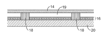
도 1에서 디스플레이 엘리먼트 어레이의 도시된 부분은 2개의 인접한 간섭계형 변조기들(12)을 포함한다. (예시된 바와 같은) 좌측상의 IMOD(12)에서, 이동가능 반사층(14)이 부분 반사층을 포함하는 광학 스택(16)으로부터 소정의 거리에서 이완 위치에 예시되어 있다. 좌측상의 IMOD(12) 양단에 인가된 전압(V0)은 이동가능 반사층(14)의 작동을 야기하는데 불충분하다. 우측상의 IMOD(12)에서, 이동가능 반사층(14)은 광학 스택(16) 근처 또는 인접한 작동 위치에 예시된다. 우측상의 IMOD(12) 양단에 인가된 전압(Vbias)은 이동가능 반사층(14)을 작동 위치에서 유지하는데 충분하다.The illustrated portion of the array of display elements in FIG. 1 includes two
도 1에서, 디스플레이 엘리먼트들(12)의 반사 특성들은 일반적으로, 디스플레이 엘리먼트들(12)상에 입사된 광, 및 좌측상의 디스플레이 엘리먼트(12)로부터 반사하는 광(15)을 나타내는 화살표들(13)로 예시되어 있다. 상세히 예시하지 않았지만, 당업자는 디스플레이 엘리먼트들(12)상에 입사한 대부분의 광(13)이 투명 기판(20)을 투과하여 광학 스택(16)으로 향할 것임을 이해할 것이다. 광학 스택(16)상에 입사한 광의 일부가 광학 스택(16)의 부분 반사층을 투과할 것이고, 일부는 투명 기판(20)을 통해 되반사된다. 광학 스택(16)을 투과하는 광(13)의 일부는 투명 기판(20)을 향해 (그리고 그를 통해) 이동가능 반사층(14)에서 되반사될 것이다. 광학 스택(16)의 부분 반사층으로부터 반사된 광과 이동가능 반사층(14)으로부터 반사된 광 사이의 간섭(보강 또는 상쇄)은 디스플레이 엘리먼트(12)로부터 반사된 광(15)의 파장(들)을 결정할 것이다.In FIG. 1, the reflective properties of the
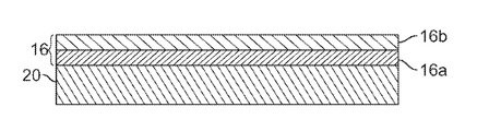
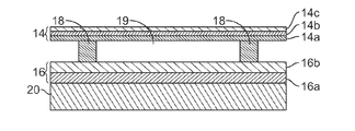
광학 스택(16)은 단일층 또는 여러 층들을 포함할 수 있다. 층(들)은 전극층, 부분 반사 및 부분 투과층 및 투명 유전체층 중 하나 또는 그 초과를 포함할 수 있다. 일부 구현들에서, 광학 스택(16)은 전기적 도전성이고, 부분 투명이고, 부분 반사형이고, 예를 들어, 상기 층들 중 하나 또는 그 초과를 투명 기판(20)상에 증착함으로써 제조될 수도 있다. 전극층은 다양한 금속들, 예를 들어, 인듐 주석 산화물(ITO)과 같은 다양한 재료들로부터 형성될 수 있다. 부분 반사층은 다양한 금속들, 예를 들어, 크롬(Cr), 반도체들, 및 유전체들과 같은 부분 반사형인 다양한 재료들로부터 형성될 수 있다. 부분 반사층은 재료들의 하나 또는 그 초과의 층들로 형성될 수 있고, 층들 각각은 단일 재료 또는 재료들의 조합으로 형성될 수 있다. 일부 구현들에서, 광학 스택(16)은 광 흡수기 및 도체 모두로서 작용하는 단일 반투명 두께의 금속 또는 반도체를 포함할 수 있지만, (예를 들어, 광학 스택(16) 또는 IMOD의 다른 구조들의) 상이한 더욱 도전성의 층들 또는 부분들이 IMOD 디스플레이 엘리먼트들 사이의 신호들을 버스(bus)하는 역할을 한다. 광학 스택(16)은 또한 하나 또는 그 초과의 도전층들 또는 도전/흡수층을 커버하는 하나 또는 그 초과의 절연 또는 유전체층들을 포함할 수 있다.
일부 구현들에서, 광학 스택(16)의 층(들)은 병렬 스트립들로 패터닝될 수 있고, 더 후술하는 바와 같이 디스플레이 디바이스에서 로우 전극들을 형성할 수도 있다. 당업자가 이해하는 바와 같이, 용어 "패터닝(patterned)"은 마스킹 뿐만 아니라 에칭 프로세스들을 지칭하는 것으로 본 명세서에서 사용된다. 일부 구현들에서, 알루미늄(Al)과 같은 고도전성 및 반사성 재료가 이동가능 반사층(14)에 대해 사용될 수도 있고, 이들 스트립들은 디스플레이 디바이스에서 컬럼 전극들을 형성할 수도 있다. 이동가능 반사층(14)은 (광학 스택(16)의 로우 전극들에 직교하는) 증착된 금속층 또는 층들의 일련의 병렬 스트립들로서 형성되어, 포스트들(18)의 상부상에 증착된 컬럼들 및 포스트들(18) 사이에 증착된 개재 희생 재료를 형성할 수도 있다. 희생 재료가 에칭될 때, 규정된 갭(19), 또는 광학 캐비티가 이동가능 반사층(14)과 광학 스택(16) 사이에 형성될 수 있다. 일부 구현들에서, 포스트들(18) 사이의 간격은 대략 1 내지 1000㎛일 수 있지만, 갭(19)은 10,000 옹스트롬(Å) 미만일 수도 있다.In some implementations, the layer (s) of the
일부 구현들에서, 작동 상태이든지 이완 상태이든지, IMOD의 각 디스플레이 엘리먼트는 본질적으로, 고정 및 이동 반사층들에 의해 형성된 커패시터이다. 전압이 인가되지 않을 때, 이동가능 반사층(14)은 이동가능 반사층(14)과 광학 스택(16) 사이의 갭(19)으로, 도 1의 좌측상에 디스플레이 엘리먼트(12)에 의해 예시되어 있는 바와 같이, 기계적으로 이완 상태에서 유지된다. 그러나, 전위차, 예를 들어, 전압이 선택된 로우 및 컬럼 중 적어도 하나에 인가될 때, 대응하는 디스플레이 엘리먼트에서 로우와 컬럼 전극들의 교차점에서 형성된 커패시터는 충전되고, 정전기력이 전극들을 함께 끌어당긴다. 인가 전압이 임계값을 초과하면, 이동가능 반사층(14)은 변형될 수 있고 광학 스택(16) 가까이 또는 그를 향해 이동할 수 있다. 광학 스택(16)내의 유전체층(미도시)이 단락을 방지할 수 있고 도 1의 우측상의 작동 디스플레이 엘리먼트(12)에 의해 예시된 바와 같이 층들(14 및 16) 사이의 분리 거리를 제어할 수 있다. 이 작용은 인가된 전위차의 극성에 관계없이 동일하다. 일부 경우들에서, 어레이에서의 일련의 디스플레이 엘리먼트들을 "로우" 또는 컬럼"으로 칭할 수도 있지만, 당업자는 "로우"로서 일 방향을 칭하고 "컬럼"으로서 다른 방향을 칭하는 것이 임의적이라는 것을 쉽게 이해할 것이다. 다시 말해, 일부 배향들에서, 로우들은 컬럼들로 고려될 수 있고, 컬럼들은 로우들로 고려될 수 있다. 또한, 디스플레이 엘리먼트들은 직교 로우들 및 컬럼들("어레이")에서 균일하게 배열될 수도 있거나, 예를 들어, 서로에 관하여 특정한 위치 오프셋들을 갖는 비선형 구성들("모자이크")로 배열될 수도 있다. 용어들 "어레이" 및 "모자이크"는 어느 구성이든 칭할 수도 있다. 따라서, 디스플레이를 "어레이" 또는 "모자이크"를 포함하는 것으로 칭하지만, 엘리먼트들 자체는 임의의 경우에서 서로 직교로 배열되거나, 균일한 분포로 배치될 필요가 없지만, 비대칭 형상들 및 불균일하게 분포된 엘리먼트들을 갖는 배열들을 포함할 수도 있다.In some implementations, whether in an operational or relaxed state, each display element of an IMOD is essentially a capacitor formed by fixed and moving reflective layers. When no voltage is applied, the movable
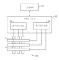
도 2는 3×3 간섭계형 변조기 디스플레이를 통합한 전자 디바이스를 예시하는 시스템 블록도의 일례를 도시한다. 전자 디바이스는 하나 또는 그 초과의 소프트웨어 모듈들을 실행하도록 구성될 수도 있는 프로세서(21)를 포함한다. 운영 시스템의 실행에 부가하여, 프로세서(21)는 웹 브라우저, 전화 애플리케이션, 이메일 프로그램, 또는 임의의 다른 소프트웨어 애플리케이션을 포함하는 하나 또는 그 초과의 소프트웨어 애플리케이션을 실행하도록 구성될 수도 있다.2 shows an example of a system block diagram illustrating an electronic device incorporating a 3x3 interferometric modulator display. The electronic device includes a
프로세서(21)는 어레이 드라이버(22)와 통신하도록 구성될 수 있다. 어레이 드라이버(22)는 신호들을 예를 들어, 디스플레이 어레이 또는 패널(30)에 제공하는 로우 드라이버 회로(24) 및 컬럼 드라이버 회로(26)를 포함할 수 있다. 도 1에 예시된 IMOD 디스플레이 디바이스의 단면은 도 2의 라인 1-1에 의해 도시된다. 도 2가 명확화를 위해 IMOD들의 3×3 어레이를 예시하지만, 디스플레이 어레이(30)는 매우 큰 수의 IMOD들을 포함할 수도 있고, 컬럼들에서와는 다른 로우들에서의 상이한 수의 IMOD들을 가질 수도 있고, 그 반대의 경우도 가능하다.The
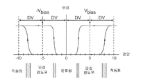
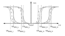
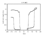
도 3은 도 1의 간섭계형 변조기에 대한 이동가능 반사층 위치 대 인가 전압을 예시하는 도면의 일례를 도시한다. MEMS 간섭계형 변조기들에 대해, 로우/컬럼(즉, 공통/세그먼트) 기록 절차는 도 3에 예시된 바와 같은 이들 디바이스들의 이력 특성을 이용할 수도 있다. 간섭계형 변조기는 이동가능 반사층 또는 미러로 하여금 이완 상태로부터 작동 상태로 변화되게 하기 위해 예를 들어, 약 10볼트의 전위차를 요구할 수도 있다. 전압이 그 값으로부터 감소될 때, 이동가능 반사층은 예를 들어, 10 볼트 아래로 전압이 강하함에 따라 그 상태를 유지하지만, 이동가능 반사층은 전압이 2 볼트 아래로 강하할 때까지 완전하게 이완하지 않는다. 따라서, 도 3에 도시되어 있는 바와 같이, 대략 3 내지 7 볼트의 전압 범위가 존재하고, 여기서, 디바이스가 이완 또는 작동 상태에서 안정한 인가 전압의 윈도우가 존재한다. 이것은 본 명세서에서, "이력 윈도우" 또는 "안정성 윈도우"로 칭한다. 도 3의 이력 특징들을 갖는 디스플레이 어레이(30)에 대해, 로우/컬럼 기록 절차는 한번에 하나 또는 그 초과의 로우들을 어드레싱하도록 설계될 수 있어서, 주어진 로우의 어드레싱 동안, 작동될 어드레싱된 로우에서의 디스플레이 엘리먼트들은 약 10 볼트의 전압차에 노출되고, 이완될 디스플레이 엘리먼트들은 제로 볼트 근처의 전압차에 노출된다. 어드레싱 이후에, 디스플레이 엘리먼트들은 정상 상태 또는 대략 5 볼트의 바이어스 전압차에 노출되어, 이들은 이전의 스트로빙(strobing) 상태에서 유지된다. 이러한 예에서, 어드레싱된 이후에, 각 디스플레이 엘리먼트는 약 3 내지 7 볼트의 "안정성 윈도우"내의 전위차를 갖는다. 이러한 이력 특성 특징은 예를 들어, 도 1에 예시된 디스플레이 엘리먼트 설계가 동일한 인가 전압 조건하에서 작동 또는 이완 기존 상태에서 안정하게 유지될 수 있게 한다. 작동 상태이든지 이완 상태이든지, 각 IMOD 디스플레이 엘리먼트는 본질적으로 고정 또는 이동 반사층들에 의해 형성된 커패시터이기 때문에, 이러한 안정한 상태는 전력을 실질적으로 소모하거나 손실하지 않고 이력 윈도우내의 정상 전압에서 홀딩될 수 있다. 더욱이, 인가 전압 전위가 실질적으로 고정되어 유지되면, IMOD 디스플레이 엘리먼트로 흐르는 전류는 본질적으로 거의 없거나 전혀 없다.3 shows an example of a diagram illustrating movable reflective layer position versus applied voltage for the interferometric modulator of FIG. 1. For MEMS interferometric modulators, the row / column (ie common / segment) writing procedure may use the hysteretic characteristics of these devices as illustrated in FIG. 3. An interferometric modulator may, for example, require a potential difference of about 10 volts to cause the movable reflective layer or mirror to change from a relaxed state to an operating state. When the voltage decreases from that value, the movable reflective layer remains in state as the voltage drops below, for example, 10 volts, but the movable reflective layer does not fully relax until the voltage drops below 2 volts. Do not. Thus, as shown in FIG. 3, there is a voltage range of approximately 3 to 7 volts, where there is a window of applied voltage in which the device is stable in a relaxed or operating state. This is referred to herein as a "history window" or "stability window." For
일부 구현들에서, 이미지의 프레임이 (만약 있다면) 원하는 변화에 따른 컬럼 전극들의 세트에 따라 "세그먼트" 전압들의 형태의 데이터 신호들을 소정의 로우에서의 디스플레이 엘리먼트들의 상태에 인가함으로써 생성될 수도 있다. 어레이의 각 로우가 차례로 어드레싱될 수 있어서, 프레임은 한번에 하나의 로우에 기록된다. 제 1 로우에서의 디스플레이 엘리먼트들에 원하는 데이터를 기록하기 위해, 제 1 로우에서의 디스플레이 엘리먼트들의 원하는 상태에 대응하는 세그먼트 전압들이 컬럼 전극들상에 인가될 수 있고, 특정한 "컬럼" 전압 또는 신호 형태의 제 1 로우 펄스가 제 1 로우 전극에 인가될 수 있다. 그 후, 세그먼트 전압들의 세트가 (만약 있다면) 원하는 변화에 대응하도록 제 2 로우에서의 디스플레이 엘리먼트들의 상태로 변화될 수도 있고, 제 2 공통 전압이 제 2 로우 전극에 인가될 수 있다. 일부 구현들에서, 제 1 로우에서의 디스플레이 엘리먼트들은 컬럼 전극들에 따라 인가된 세그먼트 전압들에서의 변화에 의해 영향을 받지 않으며, 제 1 공통 전압 동안 로우 펄스로 설정된 상태를 유지한다. 이러한 프로세스는 순차적 방식으로 전체 일련의 로우들 또는 다르게는 컬럼들에 대해 반복되어 이미지 프레임을 생성할 수도 있다. 프레임들은 초당 일부 원하는 수의 프레임들에서 이러한 프로세스를 연속적으로 반복함으로써 새로운 이미지 데이터로 리프레시되고/되거나 업데이트될 수 있다. 본 명세서에 설명하는 바와 같은 데이터 기록 및/또는 유지 프로세스에서 사용되는 각 세그먼트 전압 및 공통 전압을 "구동 방식 전압"으로 칭한다.In some implementations, a frame of the image may be generated by applying data signals in the form of “segment” voltages to a state of display elements in a given row according to the set of column electrodes according to the desired change (if any). Each row of the array can be addressed in turn, so that the frame is written to one row at a time. In order to write the desired data to the display elements in the first row, segment voltages corresponding to the desired states of the display elements in the first row can be applied on the column electrodes, and the particular "column" voltage or signal type The first low pulse of may be applied to the first low electrode. The set of segment voltages may then be changed to the state of the display elements in the second row (if any) to correspond to the desired change, and a second common voltage may be applied to the second row electrode. In some implementations, the display elements in the first row are not affected by changes in the segment voltages applied along the column electrodes and remain set to a low pulse during the first common voltage. This process may be repeated for the entire series of rows or otherwise columns in a sequential manner to generate an image frame. The frames may be refreshed and / or updated with new image data by successively repeating this process at some desired number of frames per second. Each segment voltage and common voltage used in the data recording and / or holding process as described herein is referred to as a " driven voltage ".
각 디스플레이 엘리먼트 양단에 인가된 세그먼트 및 공통 신호들의 조합(즉, 각 디스플레이 엘리먼트 양단의 전위차)은 각 디스플레이 엘리먼트의 결과적인 상태를 결정한다. 도 4는 다양한 공통 및 세그먼트 전압들이 인가될 때 간섭계형 변조기의 다양한 상태들을 예시하는 테이블의 일례를 도시한다. 당업자가 용이하게 이해하는 바와 같이, "세그먼트" 전압들은 컬럼 전극들 또는 로우 전극들 중 어느 하나에 인가될 수 있고, "공통" 전압들은 컬럼 전극들 또는 로우 전극들 중 다른 하나에 인가될 수 있다.The combination of segments and common signals applied across each display element (ie, the potential difference across each display element) determines the resulting state of each display element. 4 shows an example of a table illustrating various states of an interferometric modulator when various common and segment voltages are applied. As will be readily appreciated by those skilled in the art, "segment" voltages may be applied to either the column electrodes or the row electrodes and "common" voltages may be applied to the other of the column electrodes or row electrodes .
도 4 (뿐만 아니라 도 5b에 도시된 타이밍도)에 예시되어 있는 바와 같이, 해제 전압(release voltage)(VCREL)이 공통 라인을 따라 인가될 때, 공통 라인을 따른 모든 간섭계형 변조기 엘리먼트들은 세그먼트 라인들을 따라 인가된 전압, 즉, 높은 세그먼트 전압(VSH) 및 낮은 세그먼트 전압(VSL)에 관계없이, 다르게는 해제 또는 비작동 상태로 칭하는 이완 상태에 배치될 것이다. 특히, 해제 전압(VCREL)이 공통 라인을 따라 인가될 때, 변조기 양단의 포텐셜 전압(다르게는 디스플레이 엘리먼트 전압으로 칭함)은, 높은 세그먼트 전압(VSH) 및 낮은 세그먼트 전압(VSL) 양자가 그 디스플레이 엘리먼트에 대한 대응하는 세그먼트 라인을 따라 인가되는 경우에 이완 윈도우(도 3을 참조하면, 해제 윈도우로 또한 칭함)내에 있다.As illustrated in FIG. 4 (as well as the timing diagram shown in FIG. 5B), when a release voltage VC REL is applied along a common line, all interferometric modulator elements along the common line are segmented. Regardless of the voltage applied along the lines, that is, the high segment voltage VS H and the low segment voltage VS L , it will be placed in a relaxed state, otherwise referred to as a released or inactive state. In particular, when the release voltage VC REL is applied along a common line, the potential voltage across the modulator (also referred to as the display element voltage) is such that both high segment voltage VS H and low segment voltage VS L When applied along the corresponding segment line for that display element it is within a relaxation window (also referred to as a release window, referring to FIG. 3).
높은 홀드 전압(VCHOLD _H) 또는 낮은 홀드 전압(VCHOLD _L)과 같은 홀드 전압이 공통 라인상에 인가될 때, 간섭계형 변조기의 상태는 일정하게 유지될 것이다. 예를 들어, 이완 IMOD는 이완 위치에서 유지될 것이고, 작동 IMOD는 작동 위치에서 유지될 것이다. 홀드 전압들은, 높은 세그먼트 전압(VSH) 및 낮은 세그먼트 전압(VSL) 양자가 대응하는 세그먼트 라인을 따라 인가될 때 디스플레이 엘리먼트 전압이 안정성 윈도우내에서 유지되도록 선택될 수 있다. 따라서, 세그먼트 전압 스윙(swing), 즉, 높은 VSH와 낮은 세그먼트 전압(VSL) 사이의 차이는 포지티브 또는 네거티브 안정성 윈도우의 폭 미만이다.When the threshold voltage of the high threshold voltage (VC HOLD _H) or a low threshold voltage (VC HOLD _L) is applied to the common line, the state of the interferometric-type modulator is to be kept constant. For example, the relaxation IMOD will be maintained in the relaxed position and the working IMOD will be maintained in the working position. The hold voltages may be selected such that the display element voltage is maintained within the stability window when both the high segment voltage VS H and the low segment voltage VS L are applied along the corresponding segment line. Thus, the segment voltage swing, i.e. the difference between high VS H and low segment voltage VS L , is less than the width of the positive or negative stability window.
높은 어드레스 전압(VCADD _H) 또는 낮은 어드레싱 전압(VCADD _L)과 같은 어드레싱, 또는 작동 전압이 공통 라인상에 인가될 때, 데이터가 각각의 세그먼트 라인들을 따라 세그먼트 전압들의 인가에 의해 그 라인을 따라 변조기들에 선택적으로 기록될 수 있다. 세그먼트 전압들은 작동이 인가된 세그먼트 전압에 의존하도록 선택될 수도 있다. 어드레싱 전압이 공통 라인을 따라 인가될 때, 하나의 세그먼트 전압의 인가는 안정성 윈도우내에서 디스플레이 엘리먼트 전압을 발생시켜, 디스플레이 엘리먼트로 하여금 비작동을 유지하게 한다. 반대로, 다른 세그먼트 전압의 인가는 안정성 윈도우를 넘는 디스플레이 엘리먼트 전압을 발생시켜, 디스플레이 엘리먼트의 작동을 발생시킨다. 작동을 초래하는 특정한 세그먼트 전압은 어느 어드레싱 전압이 사용되는지에 의존하여 변할 수 있다. 일부 구현들에서, 높은 어드레싱 전압(VCADD _H)이 공통 라인을 따라 인가될 때, 높은 세그먼트 전압(VSH)의 인가는 변조기로 하여금 그것의 현재 위치에서 유지되게 할 수 있고, 낮은 세그먼트 전압(VSL)의 인가는 변조기의 작동을 초래할 수 있다. 그 결과, 세그먼트 전압들의 영향은 낮은 어드레싱 전압(VCADD _L)이 인가될 때 반대일 수 있는데, 높은 세그먼트 전압(VSH)은 변조기의 작동을 초래하고, 낮은 세그먼트 전압(VSL)은 변조기의 상태에 영향을 주지 않는다(즉, 안정을 유지한다).When a high address voltage addressing, such as (VC ADD _H) or a low addressing voltage (VC ADD _L), or the operation voltage is applied to the common line, the data for that line by the application of the segment voltage in accordance with the respective segment lines May optionally be written to the modulators. The segment voltages may be selected to depend on the segment voltage to which the operation is applied. When the addressing voltage is applied along a common line, the application of one segment voltage generates a display element voltage within the stability window, allowing the display element to remain inoperative. In contrast, the application of other segment voltages generates display element voltages beyond the stability window, resulting in operation of the display elements. The particular segment voltage that results in operation may vary depending on which addressing voltage is used. In some implementations, when a high addressing voltage (VC ADD - H ) is applied along a common line, application of a high segment voltage (VS H ) may cause the modulator to remain at its current location, VS L ) may result in operation of the modulator. As a result, the influence of the segment voltages can be reversed when a low addressing voltage VC ADD _ L is applied, where the high segment voltage VS H causes the operation of the modulator and the low segment voltage VS L It does not affect the state (i.e. maintains stability).
일부 구현들에서, 변조기들 양단에 동일한 극성의 전위차를 항상 생성하는 홀드 전압들, 어드레스 전압들, 및 세그먼트 전압들이 사용될 수도 있다. 일부 다른 구현들에서, 변조기들의 전위차의 극성을 교호시키는 신호들이 사용될 수 있다. 변조기들 양단의 극성의 교호(즉, 기록 절차들의 극성의 교호)는 단일 극성의 반복된 기록 동작들 이후에 발생할 수 있는 전하 축적을 감소시키거나 억제할 수도 있다.In some implementations, hold voltages, address voltages, and segment voltages may be used that always produce a potential difference of the same polarity across the modulators. In some other implementations, signals can be used that alternate the polarity of the potential difference of the modulators. Alternating the polarity across the modulators (ie, alternating polarity of the write procedures) may reduce or suppress charge accumulation that may occur after repeated write operations of a single polarity.
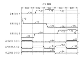
도 5a는 도 2의 3×3 간섭계형 변조기 디스플레이에서 디스플레이 데이터의 프레임을 예시하는 도면의 일례를 도시한다. 도 5b는 도 5a에 예시된 디스플레이 데이터의 프레임을 기록하기 위해 사용될 수도 있는 공통 및 세그먼트 신호들에 대한 타이밍도의 일례를 도시한다. 신호들은 예를 들어, 도 2의 3×3 어레이에 인가될 수 있고, 이는 궁극적으로 도 5a에 예시된 라인 타임(60e) 디스플레이 배열을 발생시킨다. 도 5a에서의 작동 변조기들은 어둠-상태에 있고, 즉, 여기서, 반사광의 상당한 부분은 예를 들어, 뷰어에 대해 어두운 외관을 발생시키도록 가시 스펙트럼 외부에 있다. 도 5a에 예시된 프레임을 기록하기 이전에, 디스플레이 엘리먼트들은 임의의 상태에 있을 수 있지만, 도 5b의 타이밍도에 예시된 기록 절차는 각 변조기가 해제되었고 제 1 라인 타임(60a) 이전에 비작동 상태에 상주한다는 것을 가정한다.FIG. 5A shows an example of a diagram illustrating a frame of display data in the 3 × 3 interferometric modulator display of FIG. 2. FIG. 5B shows an example of a timing diagram for common and segment signals that may be used to record the frame of display data illustrated in FIG. 5A. The signals may be applied, for example, to the 3 × 3 array of FIG. 2, which ultimately results in the
제 1 라인 타임(60a) 동안, 해제 전압(70)이 공통 라인 1상에 인가되고; 공통 라인 2상에 인가된 전압은 높은 홀드 전압(72)에서 시작하여 해제 전압(70)으로 이동하며, 낮은 홀드 전압(76)이 공통 라인 3을 따라 인가된다. 따라서, 공통 라인 1을 따라 변조기들(공통 1, 세그먼트 1)(1, 2) 및 (1, 3)은 제 1 라인 타임(60a)의 지속기간 동안 이완 또는 비작동 상태에서 유지되고, 공통 라인 2를 따른 변조기들(2, 1), (2, 2) 및 (2, 3)은 이완 상태로 이동하며, 공통 라인 3을 따른 변조기들(3, 1), (3, 2) 및 (3, 3)은 그들의 이전 상태에서 유지될 것이다. 도 4를 참조하면, 세그먼트 라인들(1, 2 및 3)을 따라 인가된 세그먼트 전압들은, 공통 라인들(1, 2 또는 3) 중 어느 것도 라인 타임(60a) 동안 작동을 초래하는 전압 레벨들에 노출되지 않기 때문에, 간섭계형 변조기들의 상태에 영향을 미치지 않을 것이다(즉, VCREL - 이완 및 VCHOLD _L - 안정).During the
제 2 라인 타임(60b) 동안, 공통 라인 1상의 전압은 높은 홀드 전압(72)으로 이동하고, 공통 라인 1을 따른 모든 변조기들은 어드레싱 또는 작동 전압이 공통 라인 1상에 인가되지 않았기 때문에 인가된 세그먼트 전압에 관계없이 이완 상태에서 유지된다. 공통 라인 2를 따른 변조기들은 해제 전압(70)의 인가로 인해 이완 상태에서 유지되고, 공통 라인 3을 따라 변조기들(3, 1), (3, 2) 및 (3, 3)은 공통 라인 3을 따른 전압이 해제 전압(70)으로 이동할 때 이완될 것이다.During the
제 3 라인 타임(60c) 동안, 공통 라인 1이 공통 라인 1상에 높은 어드레스 전압(74)을 인가함으로써 어드레싱된다. 낮은 세그먼트 전압(64)이 이러한 어드레스 전압의 인가 동안 세그먼트 라인들(1 및 2)을 따라 인가되기 때문에, 변조기들(1, 1) 및 (1, 2) 양단의 디스플레이 엘리먼트 전압은 변조기들의 포지티브 안정성 윈도우의 상단(high end)보다 크고(즉, 전압차가 소정의 임계값을 초과), 변조기들(1, 1) 및 (1, 2)은 작동된다. 반대로, 높은 세그먼트 전압(62)이 세그먼트 라인 3을 따라 인가되기 때문에, 변조기(1, 3) 양단의 디스플레이 엘리먼트 전압은 변조기들(1, 1) 및 (1, 2)의 디스플레이 엘리먼트 전압 미만이고, 변조기의 포지티브 안정성 윈도우내에서 유지되며; 따라서, 변조기(1, 3)가 이완되어 유지된다. 또한, 라인 타임(60c) 동안, 공통 라인 2를 따른 전압은 낮은 홀드 전압(76)으로 감소하고, 공통 라인 3을 따른 전압은 해제 전압(70)에서 유지되어, 공통 라인들(2 및 3)을 따른 변조기들을 이완 위치에 남겨둔다.During the third line time 60c,
제 4 라인 타임(60d) 동안, 공통 라인 1상의 전압은 높은 홀드 전압(72)으로 복귀하여, 공통 라인 1을 따른 변조기들을 그들 각각의 어드레싱된 상태들에 남겨둔다. 공통 라인 2상의 전압은 낮은 어드레스 전압(78)으로 감소된다. 높은 세그먼트 전압(62)이 세그먼트 라인 2를 따라 인가되기 때문에, 변조기(2, 2) 양단의 디스플레이 엘리먼트 전압은 변조기의 네거티브 안정성 윈도우의 하단 아래이어서, 변조기(2, 2)가 작동되게 한다. 반대로, 낮은 세그먼트 전압(64)이 세그먼트 라인들(1 및 3)을 따라 인가되기 때문에, 변조기들(2, 1) 및 (2, 3)은 이완 위치에서 유지된다. 공통 라인 3상의 전압은 높은 홀드 전압(72)으로 증가하여, 공통 라인 3을 따른 변조기들을 이완 상태에 남겨둔다.During the
마지막으로, 제 5 라인 타임(60e) 동안, 공통 라인 1상의 전압은 높은 홀드 전압(72)에서 유지되고, 공통 라인 2상의 전압은 낮은 홀드 전압(76)에서 유지되어서, 공통 라인들(1 및 2)을 따른 변조기들을 그들 각각의 어드레싱된 상태들에 남겨둔다. 공통 라인 3상의 전압은 높은 어드레스 전압(74)으로 증가하여 공통 라인 3을 따른 변조기들을 어드레싱한다. 낮은 세그먼트 전압(64)이 세그먼트 라인들(2 및 3)상에 인가되기 때문에, 변조기들(3, 2) 및 (3, 3)은 작동하고, 세그먼트 라인 1을 따라 인가된 높은 세그먼트 전압(62)은 변조기(3, 1)로 하여금 이완 위치에서 유지되게 한다. 따라서, 제 5 라인 타임(60e)의 종단에서, 3×3 디스플레이 엘리먼트 어레이는 도 5a에 도시된 상태에 있고, 다른 공통 라인들(미도시)을 따른 변조기들이 어드레싱될 때 발생할 수도 있는 세그먼트 전압에서의 변동들에 관계없이 홀드 전압들이 공통 라인들을 따라 인가되는 한은 그 상태에서 유지될 것이다.Finally, during the
도 5b의 타이밍도에서, 주어진 기록 절차(즉, 라인 타임들(60a-60e))는 높은 홀드 및 어드레스 전압들, 또는 낮은 홀드 및 어드레스 전압들의 사용을 포함할 수 있다. 기록 절차가 주어진 공통 라인에 대해 완료되면(그리고, 공통 전압이 작동 전압과 동일한 극성을 갖는 홀드 전압으로 설정되면), 디스플레이 엘리먼트 전압은 주어진 안전성 윈도우내에서 유지되고, 해제 전압이 그 공통 라인상에 인가될 때까지 이완 윈도우를 통과하지 않는다. 또한, 각 변조기가 변조기를 어드레싱하기 이전에 기록 절차의 일부로서 해제될 때, 해제 시간보다는 변조기의 작동 시간이 필요한 라인 타임을 결정할 수도 있다. 구체적으로, 변조기의 해제 시간이 작동 시간보다 큰 구현들에서, 해제 전압은 도 5b에 도시되어 있는 바와 같이, 단일 라인 시간보다 길게 인가될 수도 있다. 일부 다른 구현들에서, 공통 라인들 또는 세그먼트 라인들을 따라 인가된 전압들은 상이한 컬러들의 변조기들과 같은 상이한 변조기들의 작동 및 해제 전압들에서의 변동들을 설명하기 위해 변할 수도 있다.In the timing diagram of FIG. 5B, a given write procedure (ie,
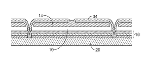
상술한 원리들에 따라 동작하는 간섭계형 변조기들의 구조의 상세는 광범위하게 변할 수도 있다. 예를 들어, 도 6a 내지 도 6e는 이동가능 반사층(14) 및 그것의 지지 구조들을 포함하는 간섭계형 변조기들의 변화하는 구현들의 단면들의 예들을 도시한다. 도 6a는 도 1의 간섭계형 변조기 디스플레이의 부분 단면도의 일례를 도시하고, 여기서, 금속 재료의 스트립, 즉, 이동가능 반사층(14)이 기판(20)으로부터 직교하게 연장하는 지지부들(18)상에 증착된다. 도 6b에서, 각 IMOD의 이동가능 반사층(14)은 일반적으로 정사각형 또는 직사각형 형상이고, 테더(tether)(32)들상의 코너들에서 또는 그 근처에서 지지부들에 부착된다. 도 6c에서, 이동가능 반사층(14)은 일반적으로 정사각형 또는 직사각형 형상이고, 플렉시블 금속을 포함할 수도 있는 변형가능층(34)으로부터 현수(suspend)되어 있다. 변형가능층(34)은 이동가능 반사층(14)의 주위에서 기판(20)에 직접 또는 간접적으로 연결될 수 있다. 본 명세서에서, 이들 연결들은 지지 포스트들이라 칭한다. 도 6c에 도시된 구현들은 이동가능층(14)의 기계적 기능들로부터 이동가능층(14)의 광학 기능들의 디커플링을 유도하는 추가의 이점들을 갖는데, 기계적 기능들은 변형가능층(34)에 의해 수행된다. 이러한 디커플링은 반사층(14)에 대해 사용된 구조적 설계 및 재료들 및 변형가능층(34)에 대해 사용된 구조적 설계 및 재료들이 서로 독립적으로 최적화되게 한다.The details of the structure of interferometric modulators operating in accordance with the principles described above may vary widely. For example, FIGS. 6A-6E show examples of cross-sections of varying implementations of interferometric modulators that include a movable
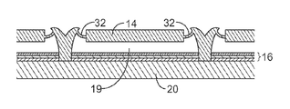
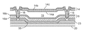
도 6d는 이동가능 반사층(14)이 반사 서브-층(14a)을 포함하는 IMOD의 다른 예를 도시한다. 이동가능 반사층(14)은 지지 포스트들(18)과 같은 지지 구조상에 놓여 있다. 지지 포스트들(18)은 하위 정지 전극(즉, 예시된 IMOD에서의 광학 스택(16)의 일부)로부터 이동가능 반사층(14)의 분리를 제공하여, 예를 들어, 이동가능 반사층(14)이 이완 위치에 있을 때 갭(19)이 이동가능 반사층(14)과 광학 스택(16) 사이에 형성된다. 이동가능 반사층(14)은 또한, 전극으로서 기능하도록 구성될 수도 있는 도전층(14c) 및 지지층(14b)을 포함할 수 있다. 이러한 예에서, 도전층(14c)은 기판(20)으로부터 먼 지지층(14b)의 일측상에 배치되고, 반사 서브층(14a)은 기판(20)에 인접한 지지층(14b)의 다른 측상에 배치된다. 일부 구현들에서, 반사 서브층(14a)은 도전성일 수 있고 지지층(14b)과 광학 스택(16) 사이에 배치될 수 있다. 지지층(14b)은 유전체 재료, 예를 들어, 실리콘 옥시나이트라이드(SiON) 또는 실리콘 디옥사이드(SiO2)의 하나 또는 그 초과의 층들을 포함할 수 있다. 일부 구현들에서, 지지층(14b)은 예를 들어, SiO2/SiON/SiO2 삼층 스택과 같은 층들의 스택일 수 있다. 반사 서브-층(14a) 및 도전층(14c) 중 하나 또는 양자는 예를 들어, 약 0.5% 구리(Cu) 또는 다른 반사형 금속 재료를 갖는 알루미늄(Al) 합금을 포함할 수 있다. 유전체 지지층(14b) 상하에 도전층들(14a, 14c)을 채용하는 것은 스트레스(stress)들을 밸런싱할 수 있고 강화된 전도성을 제공할 수 있다. 일부 구현들에서, 반사 서브층(14a) 및 도전층(14c)은 이동가능 반사층(14)내에서 특정한 스트레스 프로파일들을 달성하는 것과 같은, 다양한 설계 목적들을 위해 상이한 재료들로 형성될 수 있다.6D shows another example of an IMOD where the movable
도 6d에 예시되어 있는 바와 같이, 일부 구현들은 또한 블랙 마스크 구조(23)를 포함할 수 있다. 블랙 마스크 구조(23)는 환경광 또는 미광을 흡수하기 위해 광학적 비활성 영역들에(즉, 디스플레이 엘리먼트들 사이 또는 포스트들(18) 아래에) 형성될 수 있다. 블랙 마스크 구조(23)는 또한, 광이 디스플레이 비활성 부분들로부터 반사되거나 그를 통해 투과하는 것을 억제함으로써 디스플레이 디바이스의 광학 특성들을 향상시킬 수 있어서, 콘트라스트비를 증가시킨다. 추가로, 블랙 마스크 구조(23)는 도전성일 수 있고 전기적 버싱(bussing)층으로서 기능하도록 구성될 수 있다. 일부 구현들에서, 로우 전극들은 블랙 마스크 구조(23)에 접속될 수 있어서 접속된 로우 전극의 저항을 감소시킨다. 블랙 마스크 구조(23)는 증착 및 패터닝 기법들을 포함하는 다양한 방법들을 사용하여 형성될 수 있다. 블랙 마스크 구조(23)는 하나 또는 그 초과의 층들을 포함할 수 있다. 예를 들어, 일부 구현들에서, 블랙 마스크 구조(23)는 광학 흡수기로서 기능하는 몰리브덴-크롬(MoCr)층, 층, 및 반사기 및 버싱층으로서 기능하는 알루미늄 합금을 포함하는데, 이들 층들은 각각 약 30 내지 80Å, 500 내지 1000Å, 및 500 내지 6000Å의 범위의 두께를 갖는다. 하나 또는 그 초과의 층들은 예를 들어, MoCr 및 SiO2층에 대해 사불화탄소(CF4) 및/또는 산소(O2) 및 알루미늄 합금층에 대해 염소(Cl2) 및/또는 삼염화 붕소(BCl3)를 포함하는, 포토리소그래피 및 건식 에칭을 포함하는 다양한 기법들을 사용하여 패터닝될 수 있다. 일부 구현들에서, 블랙 마스크(23)는 에탈론(etalon) 또는 간섭계형 스택 구조일 수 있다. 이러한 간섭계형 스택 블랙 마스크 구조들(23)에서, 도전성 흡수기들은 각 로우 또는 컬럼의 광학 스택(16)에서 하위 정지 전극들 사이에서 신호들을 송신하거나 버싱하기 위해 사용될 수 있다. 일부 구현들에서, 스페이서 층(35)이 흡수기 층(16a)을 블랙 마스크(23)에서의 도전층들로부터 전기적으로 절연시키도록 일반적으로 기능할 수 있다.As illustrated in FIG. 6D, some implementations may also include a
도 6e는 이동가능 반사층(14)이 자체 지지하는 IMOD의 다른 예를 도시한다. 도 6d와 반대로, 도 6e의 구현은 지지 포스트들(18)을 포함하지 않는다. 대신에, 이동가능 반사층(14)은 다수의 위치들에서 기반 광학 스택(16)에 접촉하고, 이동가능 반사층(14)의 곡률은 간섭계형 변조기 양단의 전압이 작동을 야기하는데 불충분할 때 이동가능 반사층(14)이 도 6e의 비작동 위치로 복귀시키는 충분한 지지를 제공한다. 광학 흡수기(16a) 및 유전체(16b)를 포함하는 복수의 여러 상이한 층들을 포함할 수도 있는 광학 스택(16)이 명확화를 위해 여기에 도시되어 있다. 일부 구현들에서, 광학 흡수기(16a)는 고정 전극 및 부분 반사층 양자로서 기능할 수도 있다.6E shows another example of an IMOD that the movable
도 6a 내지 도 6e에 도시된 바와 같은 구현들에서, IMOD들은 이미지들이 투명 기판(20)의 전면, 즉, 변조기가 배열되는 측에 대향하는 측으로부터 관측되는 직시형 디바이스들로서 기능한다. 이들 구현들에서, 디바이스의 백(back) 부분들(즉, 예를 들어, 도 6c에 예시된 변형가능층(34)을 포함하는 이동가능 반사층(14) 뒤의 디스플레이 디바이스의 임의의 부분)은, 반사층(14)이 디바이스의 이들 부분들을 광학적으로 차폐하기 때문에, 디스플레이 디바이스의 이미지 품질에 영향을 주거나 악영향을 미치지 않고 구성되고 동작될 수 있다. 예를 들어, 일부 구현들에서, 버스 구조(미도시)가 전압 어드레스 및 이러한 어드레싱으로부터 발생하는 이동들과 같은, 변조기의 전자기계적 특성들로부터 변조기의 광학 특성을 분리하는 능력을 제공하는 이동가능 반사층(14) 뒤에 포함될 수 있다. 추가로, 도 6a 내지 도 6e의 구현들은 예를 들어, 패터닝과 같은 프로세싱을 단순화할 수 있다.In implementations as shown in FIGS. 6A-6E, the IMODs function as direct view devices where images are viewed from the front side of the
도 7은 간섭계형 변조기에 대한 제조 프로세스(80)를 예시하는 흐름도의 일례를 도시하고, 도 8a 내지 도 8e는 이러한 제조 프로세스(80)의 대응하는 스테이지들의 개략적 단면 예시들의 예들을 도시한다. 일부 구현들에서, 제조 프로세스(80)는 도 7에 도시되지 않은 다른 블록들에 부가하여, 예를 들어, 도 1 및 도 6에 예시된 일반형의 간섭계형 변조기들을 제조하기 위해 구현될 수 있다. 도 1, 도 6, 및 도 7을 참조하면, 프로세스(80)는 기판(20)상에 광학 스택(16)의 형성으로 블록 82에서 시작한다. 도 8a는 기판(20)상에 형성된 이러한 광학 스택(16)을 예시한다. 기판(20)은 유리 또는 플라스틱과 같은 투명 기판일 수도 있고, 플렉시블하거나 비교적 강성(stiff)이고 굴곡되지 않을(unbending) 수도 있고, 광학 스택(16)의 효율적인 형성을 용이하게 하기 위해 이전의 준비 프로세스들, 예를 들어, 클리닝을 받을 수도 있다. 상기 논의한 바와 같이, 광학 스택(16)은 전기적 도전성이고, 부분 투명이고, 부분 반사형일 수 있고, 예를 들어, 원하는 특성들을 갖는 하나 또는 그 초과의 층들을 투명 기판(20)상에 증착함으로써 제조될 수도 있다. 도 8a에서, 광학 스택(16)은, 다소의 서브층들이 일부 다른 구현들에 포함될 수도 있지만, 서브층들(16a 및 16b)을 갖는 다층 구조를 포함한다. 일부 구현들에서, 서브층들(16a, 16b) 중 하나는 결합된 도체/흡수기 서브층(16a)과 같은, 광학적으로 흡수 및 도전 특성들 양자를 갖고 구성될 수 있다. 추가로, 서브층들(16a, 16b) 중 하나 또는 그 초과는 병렬 스트립들로 패터닝될 수 있고, 디스플레이 디바이스에서 로우 전극들을 형성할 수도 있다. 이러한 패터닝은 마스킹 및 에칭 프로세스 또는 당업계에 알려진 다른 적합한 프로세스에 의해 수행될 수 있다. 일부 구현들에서, 서브층들(16a, 16b) 중 하나는 하나 또는 그 초과의 금속층들(예를 들어, 하나 또는 그 초과의 반사 및/또는 도전층들)상에 증착되는 서브층(16b)과 같은 절연 또는 유전체층일 수 있다. 또한, 광학 스택(16)은 디스플레이의 로우들을 형성하는 개별 및 병렬 스트립들로 패터닝될 수 있다.7 shows an example of a flow diagram illustrating a
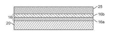
프로세스(80)는 광학 스택(16)상에 희생층(125)을 형성하는 블록 84로 계속된다. 희생층(25)은 캐비티(19)를 형성하기 위해 추후 제거되고(예를 들어, 블록 90에서), 따라서, 희생층(25)은 도 1에 예시된 결과적인 간섭계형 변조기들(12)에서는 도시되지 않는다. 도 8b는 광학 스택(16)상에 형성된 희생층(25)을 포함하는 부분 제조된 디바이스를 예시한다. 광학 스택(16)상의 희생층(25)의 형성은 후속 제거 이후에, 원하는 설계 사이즈를 갖는 갭 또는 캐비티(19)(도 1 및 도 8e를 또한 참조)를 제공하도록 선택된 두께로, 이불화 크세논(XeF2) - 몰리브덴(Mo) 또는 비정질 실리콘(a-Si)과 같은 에칭가능 재료의 증착을 포함할 수도 있다. 희생층의 증착은 물리 기상 증착(PVD, 예를 들어, 스퍼터링), 플라즈마 강화 화학 기상 증착(PECVD), 열화학 기상 증착(열 CVD), 또는 스핀-코팅과 같은 증착 기법들을 사용하여 수행될 수도 있다.
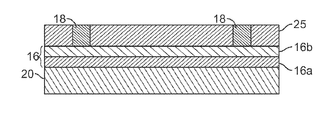
프로세스(80)는 도 1, 도 6 및 도 8c에 예시된 바와 같이 지지 구조, 예를 들어, 포스트(18)를 형성하는 블록 86에서 계속된다. 포스트(18)의 형성은 지지 구조 개구를 형성하기 위한 희생층(25)의 패터닝, 그 후, 포스트(18)를 형성하기 위한 개구로의 재료(예를 들어, 폴리머 또는 무기 재료, 예를 들어, 실리콘 산화물)의 증착, PVD, PECVD, 열 CVD와 같은 증착 방법, 또는 스핀-코팅의 사용을 포함할 수도 있다. 일부 구현들에서, 희생층에 형성된 지지 구조 개구는 희생층(25) 및 광학 스택(16) 양자를 통해 기반 기판(20)으로 연장할 수 있어서, 포스트(18)의 하위단이 도 6a에 예시되어 있는 바와 같이 기판(20)에 접촉한다. 다르게는, 도 8c에 도시된 바와 같이, 희생층(25)에 형성된 개구는 희생층(25)을 통하지만 광학 스택(16)은 통하지 않고 연장할 수 있다. 예를 들어, 도 8e는 광학 스택(16)의 상부 표면과 접촉하는 지지 포스트들(18)의 하위단들을 예시한다. 포스트(18), 또는 다른 지지 구조들은 희생층(25)상에 지지 구조 재료의 층을 증착하고, 희생층(25)의 개구로부터 떨어져 위치된 지지 구조 재료의 부분들을 패터닝함으로써 형성될 수도 있다. 지지 구조들은 도 8c에 예시되어 있는 바와 같이 개구들내에 위치될 수도 있지만, 희생층(25)의 부분상으로 적어도 부분적으로 또한 연장할 수 있다. 상기 언급한 바와 같이, 희생층(25) 및/또는 지지 포스트들(18)의 패터닝은 패터닝 및 에칭 프로세스에 의해 수행될 수 있지만, 대안의 에칭 방법들에 의해 또한 수행될 수도 있다.
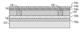
프로세스(80)는 도 1, 도 6 및 도 8d에 예시된 이동가능 반사층(14)과 같은 이동가능 반사층 또는 멤브레인을 형성하는 블록 88에서 계속된다. 이동가능 반사층(14)은 하나 또는 그 초과의 증착 단계들, 예를 들어, 하나 또는 그 초과의 패터닝, 마스킹, 및/또는 에칭 단계들과 함께 반사층(예를 들어, 알루미늄, 알루미늄 합금) 증착을 이용함으로써 형성될 수도 있다. 이동가능 반사층(14)은 전기적 도전성일 수 있고, 전기적 도전층으로 칭할 수 있다. 일부 구현들에서, 이동가능 반사층(14)은 도 8d에 도시되어 있는 바와 같이 복수의 서브층들(14a, 14b, 14c)을 포함할 수도 있다. 일부 구현들에서, 서브층들(14a, 14c)과 같은 서브층들 중 하나 또는 그 초과는 이들의 광학 특성들을 위해 선택된 고반사 서브층들을 포함할 수도 있고, 다른 서브층(14b)은 그것의 기계적 특성들을 위해 선택된 기계적 서브층을 포함할 수도 있다. 희생층(25)이 블록 88에서 형성된 부분 제조된 간섭계형 변조기에 여전히 존재하기 때문에, 이동가능 반사층(14)은 통상적으로 이러한 스테이지에서 이동가능하지 않다. 희생층(25)을 포함하는 부분 제조된 IMOD를 본 명세서에서 "비해제(unreleased)" IMOD로 또한 칭할 수도 있다. 도 1과 관련하여 상술한 바와 같이, 이동가능 반사층(14)은 디스플레이의 컬럼들을 형성하는 개별 및 병렬 스트립들로 패터닝될 수 있다.
프로세스(80)는 도 1, 도 6 및 도 8e에 예시된 바와 같이 캐비티, 예를 들어, 캐비티(19)를 형성하는 블록 90에서 계속된다. 캐비티(19)는 (블록 84에서 증착된) 희생층(25)을 에천트에 노출시킴으로써 형성될 수도 있다. 예를 들어, Mo 또는 비정질 Si와 같은 에칭가능한 희생 재료가 예를 들어, 캐비티(19)를 둘러싸는 구조들에 대해 통상적으로 선택적으로 제거된, 원하는 양의 재료를 제거하는데 유효한 기간 동안 고체 XeF2로부터 유도된 증기와 같은 가스 또는 증기 에천트에 희생층(25)을 노출시킴으로써 건식 화학적 에칭에 의해 제거될 수도 있다. 다른 에칭 방법들, 예를 들어, 습식 에칭 및/또는 플라즈마 에칭이 또한 사용될 수도 있다. 희생층(25)이 블록 90 동안 제거되기 때문에, 이동가능한 반사층(14)은 통상적으로 이러한 스테이지 이후에 이동가능하다. 희생 재료(25)의 제거 이후에, 결과적인 완전 또는 부분 제조 IMOD를 본 명세서에서 "해제" IMOD로 칭할 수도 있다.
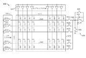
도 9는 픽셀 디스플레이 당 64 컬러의 구현을 구동시키는 공통 드라이버(904) 및 세그먼트 드라이버(902)의 예들을 예시하는 블록도이다. 어레이는 일부 구현들에서, 간섭계형 변조기들을 포함할 수도 있는 전자기계 디스플레이 엘리먼트들(102)의 세트를 포함할 수 있다. 세그먼트 전극들 또는 세그먼트 라인들(122a-122d, 124a-124d, 126a-126d)의 세트 및 공통 전극들 또는 공통 라인들(112a-112d, 114a-114d, 116a-116d)의 세트는, 각 디스플레이 엘리먼트가 다수의 세그먼트 전극들 및 공통 전극들과 전기적 통신하고 있을 것이기 때문에, 디스플레이 엘리먼트들(102)을 어드레싱하기 위해 사용될 수 있다. 세그먼트 드라이버 회로(902)는 세그먼트 전극들 각각의 양단에 전압 파형들을 인가하도록 구성되고, 공통 드라이버 회로(904)는 공통 전극들 각각의 양단에 전압 파형들을 인가하도록 구성된다. 일부 구현들에서, 세그먼트 전극들(122a 및 124a)과 같은, 세그먼트 전극들 중 일부가 서로 전기적 통신하고 있을 수도 있어서, 동일한 전압 파형이 세그먼트 전극들 각각의 양단에 동시에 인가될 수 있다. 2개의 세그먼트 전극들에 커플링되기 때문에, 2개의 세그먼트 전극들에 접속된 세그먼트 드라이버 출력들을, 이러한 세그먼트 출력의 상태가 각 로우에서 2개의 인접하는 디스플레이 엘리먼트들의 상태를 제어하기 때문에, 본 명세서에서 "최상위 비트"(MSB) 세그먼트 출력이라 칭할 수도 있다. 126a에서와 같이 개별 세그먼트 전극들에 커플링된 세그먼트 드라이버 출력들을 이들이 각 로우에서 단일 디스플레이 엘리먼트의 상태를 제어하기 때문에 본 명세서에서 "최하위 비트"(LSB) 전극들이라 칭할 수도 있다.9 is a block diagram illustrating examples of
도 9를 여전히 참조하면, 디스플레이가 컬러 디스플레이 또는 단색 그레이스케일 디스플레이를 포함하는 구현에서, 전자기계 엘리먼트들(102)의 그룹들은 다양한 컬러들 또는 그레이스케일들을 디스플레이할 수 있는 픽셀들을 형성할 수도 있다. 본 명세서에서 사용되는 바와 같이, 디스플레이 엘리먼트는 이미지 기록 프로세스 동안 정의된 상태에 투입되는 단일 디바이스를 칭한다. 반사 또는 흡수 상태에 투입될 수 있는 개별 간섭계형 변조기가 일례이다. 픽셀은 이미지 데이터의 특정한 피스 또는 영역을 시각적으로 표현하기 위해 사용되는 하나 또는 그 초과의 디스플레이 엘리먼트들의 집합이다. 컬러 또는 그레이스케일 디스플레이를 위해, 이미지 데이터의 각 입력 픽셀은 이미지 데이터에 의해 정의된 그레이 레벨 또는 컬러의 시각적 표현을 (직접적으로 또는 주위 픽셀들과 결합하여) 생성하기 위해 사용되는 어레이 픽셀을 정의하는 디스플레이 엘리먼트들의 그룹에 매핑될 수도 있다. 단일 디스플레이 엘리먼트가 픽셀로서 그 자체로 기능하는 것이 가능하지만, 일반적으로 상이한 컬러들을 갖는 디스플레이 엘리먼트들의 그룹들이 가장 일반적으로 사용된다.Still referring to FIG. 9, in an implementation where the display includes a color display or a monochrome grayscale display, groups of
어레이가 컬러 디스플레이를 포함하는 구현에서, 다양한 컬러들은 공통 라인들을 따라 정렬될 수도 있어서, 주어진 공통 라인을 따라 실질적으로 모든 디스플레이 엘리먼트들은 동일한 컬러를 디스플레이하도록 구성된 디스플레이 엘리먼트들을 포함한다. 컬러 디스플레이들의 일부 구현들은 적색, 녹색, 및 청색 디스플레이 엘리먼트들의 교호하는 라인들을 포함한다. 예를 들어, 라인들(112a-112d)은 적색 간섭계형 변조기들의 라인들에 대응할 수도 있고, 라인들(114a-114d)은 녹색 간섭계형 변조기들의 라인들에 대응할 수도 있으며, 라인들(116a-116d)은 청색 간섭계형 변조기들의 라인들에 대응할 수도 있다. 일 구현에서, 간섭계형 변조기들(102)의 각 3×3 어레이는 픽셀들(130a-130d)과 같은 픽셀을 형성한다. 세그먼트 전극들 중 2개가 서로 단락되는 예시된 구현에서, 이러한 3×3 픽셀은 각 픽셀에서 각 공통 전극을 따른 3개의 공통 컬러 디스플레이 엘리먼트들의 각 세트가 0, 1, 2, 또는 3개의 작동 간섭계형 변조기들에 대응하는 4개의 상이한 상태들에 배치될 수 있기 때문에, 64개의 상이한 컬러들(예를 들어, 6-비트 컬러 깊이)을 렌더링할 수 있을 것이다. 단색 그레이스케일 모드에서 이러한 배열을 사용할 때, 각 컬러에 대한 3개의 픽셀 세트들의 상태는 동일하도록 이루어지고, 이러한 경우에, 각 픽셀은 4개의 상이한 그레이 레벨 강도들을 채용할 수 있다. 이것은 단지 하나의 예이며, 간섭계형 변조기들의 더 큰 그룹들이 상이한 전체 픽셀 카운트 또는 해상도를 갖는 더 큰 컬러 범위를 갖는 픽셀들을 형성하기 위해 사용될 수도 있다는 것이 이해될 것이다.In an implementation where the array includes a color display, the various colors may be aligned along common lines such that substantially all display elements along a given common line include display elements configured to display the same color. Some implementations of color displays include alternating lines of red, green, and blue display elements. For example,
상세히 상술한 바와 같이, 디스플레이 데이터의 라인을 기록하기 위해, 세그먼트 드라이버(902)는 세그먼트 전극들 또는 그에 접속된 버스들에 전압들을 인가할 수도 있다. 그 후, 공통 드라이버(904)는 그에 접속된 선택된 공통 라인을 펄싱하여, 예를 들어, 각각의 세그먼트 출력들에 인가된 전압들에 따라 라인을 따른 선택된 디스플레이 엘리먼트들을 작동시킴으로써, 선택된 라인을 따른 디스플레이 엘리먼트들로 하여금 데이터를 디스플레이하게 할 수도 있다.As described above in detail, to write a line of display data, the
디스플레이 데이터가 선택된 라인에 기록된 이후에, 세그먼트 드라이버(902)는 그에 접속된 버스들에 다른 전압들의 세트를 인가할 수도 있고, 공통 드라이버(904)는 다른 라인에 디스플레이 데이터를 기록하기 위해 그에 접속된 다른 라인을 펄싱할 수도 있다. 이러한 프로세스를 반복함으로써, 디스플레이 데이터는 디스플레이 어레이의 임의의 수의 라인들에 순차적으로 기록될 수도 있다.After the display data is written to the selected line, the
이러한 프로세스를 사용하여 디스플레이 어레이에 (기록 시간으로서 또한 알려진) 디스플레이 데이터를 기록하는 시간은 기록된 디스플레이 데이터의 라인들의 수에 일반적으로 비례한다. 그러나, 많은 애플리케이션들에서, 예를 들어, 디스플레이의 프레임 레이트를 증가시키거나 임의의 인지가능한 플리커를 감소시키기 위해 기록 시간을 감소시키는 것이 바람직할 수도 있다.The time to write display data (also known as write time) to the display array using this process is generally proportional to the number of lines of display data written. However, in many applications, it may be desirable to reduce the write time, for example, to increase the frame rate of the display or to reduce any perceptible flicker.
도 10은 간섭계형 변조기들의 어레이의 여러 부재들에 대한 이동가능 반사 미러 위치 대 인가 전압을 예시하는 도면의 일례를 도시한다. 도 10은 도 3과 유사하지만, 어레이에서 상이한 변조기들 중에서 이력 곡선들의 변동들을 예시한다. 본 명세서에서 사용되는 바와 같이, 용어 "구동 응답 특징"은 인가 전기 신호에 대한 디스플레이 엘리먼트의 응답의 특징을 칭한다. 본 명세서에서 설명하는 간섭계형 변조기 디스플레이 엘리먼트들에 대해, 인가 신호는 전압이고, 구동 응답 특징들은 디스플레이 엘리먼트들 중 하나 또는 그룹에 대한 이력 곡선(들)의 형상 및 위치와 관련된다. 각 간섭계형 변조기가 일반적으로 이력을 나타내지만, 이력 윈도우의 에지들은 어레이의 모든 변조기들에 대해 동일한 전압들에 있지 않다. 따라서, 작동 전압들 및 해제 전압들은 어레이의 상이한 간섭계형 변조기들에 대해, 심지어 공칭적으로 동일한 것으로 의도되는 간섭계형 변조기들에 대해 상이할 수도 있다. 이러한 불균일성은 예를 들어, 제조 프로세스에서 반드시 발생하는 재료 두께들에서의 약간의 차이들 또는 어레이의 상이한 부분들에서의 다른 특성들로부터 발생할 수도 있다. 또한, 작동 전압들 및 해제 전압들은 디스플레이의 온도, 노화, 및 사용 패턴들에서의 변동들로 그 수명 동안 변할 수 있다. 이것은 도 4와 관련하여 상술한 구동 방식과 같은 구동 방식에서 사용될 전압들을 결정하는 것을 어렵게 만들 수 있다. 이것은 또한, 디스플레이 어레이의 사용 동안 및 그 수명 동안 이들 변화들을 트랙킹하는 방식으로 구동 방식에서 사용된 전압들을 변화시키는 것을 최적의 디스플레이 동작에 유용하게 할 수 있다.10 shows an example of a diagram illustrating movable reflective mirror position versus applied voltage for various members of an array of interferometric modulators. FIG. 10 is similar to FIG. 3, but illustrates variations in hysteresis curves among different modulators in the array. As used herein, the term "drive response feature" refers to a feature of the response of the display element to an applied electrical signal. For the interferometric modulator display elements described herein, the application signal is a voltage and the drive response characteristics are related to the shape and position of the hysteresis curve (s) for one or a group of display elements. While each interferometric modulator typically exhibits a hysteresis, the edges of the hysteresis window are not at the same voltages for all modulators in the array. Thus, operating voltages and release voltages may be different for different interferometric modulators of the array, even for interferometric modulators that are intended to be nominally the same. Such nonuniformity may arise, for example, from slight differences in material thicknesses necessarily occurring in the manufacturing process or other properties in different parts of the array. In addition, operating voltages and release voltages may change over their lifetime due to variations in the temperature, aging, and usage patterns of the display. This can make it difficult to determine the voltages to be used in a drive scheme such as the drive scheme described above with respect to FIG. 4. It may also be useful for optimal display operation to vary the voltages used in the drive scheme in a way that tracks these changes during use and during its lifetime.
이제, 도 10으로 돌아가서, (도 11에서 VCENT로 표기된) 중심 전압 초과의 포지티브 작동 전압 및 중심 전압 미만의 네거티브 작동 전압에서, 각 간섭계형 변조기는 해제 상태로부터 작동 상태로 변화한다. 중심 전압은 포지티브 이력 윈도우와 네거티브 이력 윈도우 사이의 중간점이다. 이것은 다양한 방식들, 예를 들어, 외부 에지들 사이의 중간, 내부 에지들 사이의 중간, 또는 2개의 윈도우들의 중간점들 사이의 중간으로 정의될 수 있다. 변조기들의 어레이에 대해, 중심 전압은 어레이의 상이한 변조기들에 대한 평균 중심 전압으로서 정의될 수도 있거나, 모든 변조기들에 대한 이력 윈도우들의 극단들 사이의 중간으로서 정의될 수도 있다. 예를 들어, 도 10을 참조하면, 중심 전압은 높은 작동 전압과 낮은 작동 전압 사이의 중간으로서 정의될 수도 있다. 실질적인 문제로서, 이러한 값이 어떻게 결정되는지는 특별하게 중요하지 않은데 그 이유는 간섭계형 변조기에 대한 중심 전압은 통상적으로 제로에 근접하고, 심지어 이러한 경우가 아니더라도, 이력 윈도우들 사이의 중간점을 계산하는 다양한 방법들이 실질적으로 동일한 값에 도달하기 때문이다. 중심 전압이 제로로부터 오프셋되는 구현들에서, 이러한 편차를 전압 오프셋으로 칭할 수도 있다.Now, returning to FIG. 10, at the positive operating voltage above the center voltage (marked V CENT in FIG. 11) and the negative operating voltage below the center voltage, each interferometric modulator changes from an off state to an active state. The center voltage is the midpoint between the positive history window and the negative history window. This can be defined in various ways, for example, between the outer edges, between the inner edges, or between the midpoints of the two windows. For an array of modulators, the center voltage may be defined as the average center voltage for the different modulators of the array, or as intermediate between the extremes of the history windows for all modulators. For example, referring to FIG. 10, the center voltage may be defined as intermediate between the high and low operating voltages. As a practical matter, it is not particularly important how this value is determined because the center voltage for the interferometric modulator is typically close to zero, and even if this is not the case, calculating the midpoint between the history windows. This is because the various methods reach substantially the same value. In implementations in which the center voltage is offset from zero, this deviation may be referred to as the voltage offset.
상술한 바와 같이, 이들 값들은 상이한 간섭계형 변조기들에 대해 상이하다. 도 10에서 각각 VAMAX _H 및 VAMAX _L로 지정된 어레이에 대한 최대 포지티브 및 네거티브 작동 전압을 특징화하는 것이 가능하다. 전압(VAMAX _H)은 어레이의 모든 변조기들(또는 더 후술하는 바와 같은 어레이의 선택된 부분)로 하여금 작동하게 하는 포지티브 극성 전압으로서 특징화될 수 있다. 전압(VAMAX _L)은 어레이의 모든 변조기들(또는 어레이의 부분)로 하여금 작동하게 하는 네거티브 극성 전압으로서 특징화될 수 있다. 이러한 용어를 사용하여, 중심 전압(VCENT)은 (VAMAX _H + VAMAX _L)/2로서 정의될 수도 있다. 이들 파라미터들 각각은 어레이의 디스플레이 엘리먼트들의 구동 응답 특징들의 예들이다.As mentioned above, these values are different for different interferometric modulators. Also characterized by the maximum positive and negative operating voltages for an array designated as VA and VA MAX MAX _H _L respectively at 10, it is possible to screen. The voltage VA MAX _H may be characterized as a positive polarity voltage that causes all modulators (or selected portions of the array as described below) of the array to operate. The voltage VA MAX _ L may be characterized as a negative polarity voltage that causes all modulators (or portions of the array) of the array to operate. Using these terms, the center voltage (V CENT) may be defined as a / 2 (VA MAX _H + VA MAX _L). Each of these parameters are examples of drive response characteristics of the display elements of the array.
도 10에서 각각 VAMIN _H 및 VAMIN _L로 지정된 어레이에 대한 최소 포지티브 및 네거티브 작동 전압을 특징화하는 것이 또한 가능하다. 전압(VAMIN _H)은 어레이의 변조기들 중 제 1 변조기(또는 어레이의 선택된 부분)만으로 하여금 작동하게 하는 포지티브 극성 전압으로서 특징화될 수 있다. 전압(VAMIN _L)은 어레이의 변조기들 중 제 1 변조기(또는 어레이의 선택된 부분)만으로 하여금 작동하게 하는 네거티브 극성 전압으로서 특징화될 수 있다.In Figure 10, to characterize at least the positive and negative operating voltages for an array designated as VA and VA MIN MIN _H _L respectively are also possible. The voltage VA MIN _ H may be characterized as a positive polarity voltage that causes only the first modulator (or selected portion of the array) to operate. The voltage VA MIN _ L may be characterized as a negative polarity voltage that causes only the first modulator (or selected portion of the array) to operate.
도 10에 또한 도시되어 있는 바와 같이, 중심 전압을 초과한 포지티브 극성 해제 전압 및 중심 전압 미만의 네거티브 극성 해제 전압에서, 간섭계형 변조기는 작동 상태로부터 해제 상태로 변화한다. 포지티브 및 네거티브 작동 전압들과 마찬가지로, 어레이에 대한 포지티브 및 네거티브 해제 전압들의 제한들을 특징화하는 것이 가능하다. 전압(VRMAX _H)은 어레이의 변조기들 중 제 1 변조기(또는 어레이의 선택된 부분)만으로 하여금 작동 상태로부터 해제되게 하게 하는 포지티브 극성 전압으로서 특징화될 수 있다. 전압(VRMAX _L)은 어레이의 변조기들 중 제 1 변조기(또는 어레이의 선택된 부분)만으로 하여금 작동 상태로부터 해제되게 하게 하는 네거티브 극성 전압으로서 특징화될 수 있다. 전압(VRMIN _H)은 어레이의 모든 변조기들(또는 어레이의 선택된 부분)로 하여금 해제되게 하는 포지티브 극성 전압으로서 특징화될 수 있다. 전압(VRMIN _L)은 어레이의 모든 변조기들(또는 어레이의 선택된 부분)로 하여금 해제되게 하는 네거티브 극성 전압으로서 특징화될 수 있다.As also shown in FIG. 10, at a positive polarity release voltage above the center voltage and a negative polarity release voltage below the center voltage, the interferometric modulator changes from an operating state to a released state. As with the positive and negative operating voltages, it is possible to characterize the limitations of the positive and negative release voltages for the array. The voltage VR MAX _H may be characterized as a positive polarity voltage that causes only the first modulator (or selected portion of the array) of the modulators of the array to be released from operation. The voltage VR MAX _ L may be characterized as a negative polarity voltage that causes only the first modulator (or selected portion of the array) of the array's modulators to be released from operation. The voltage VR MIN _ H may be characterized as a positive polarity voltage that causes all modulators (or selected portions of the array) of the array to be released. The voltage VR MIN _ L may be characterized as a negative polarity voltage that causes all modulators (or selected portions of the array) of the array to be released.
도 11은 간섭계형 변조기들의 어레이의 여러 부재들에 대한 이동가능 반사 미러 위치 대 인가 전압을 개념적으로 예시하는 도면의 다른 예를 도시한다. 도 11은 또한 어레이의 변조기들에 존재하는 이력 곡선들의 범위에 대한 상이한 구동 방식 전압들 및 그들의 관계를 도시한다. 도 11에서, 이력 특징들의 범위는 상술한 바와 동일한 의미를 갖는 VAMAX _H, VAMAX _L, VAMIN _H, VAMIN _L, VRMAX _H, VRMAX _L, VRMIN _H, 및 VRMIN_L로 평행사변형으로서 표현된다. 도 11에서 거리(AL)는 구동 신호들에서 잡음, 파형 왜곡들 등의 존재에도 일부 변조기들의 갑작스런 해제를 회피하기 위해 홀드 상태 동안 구동 방식이 변조기들에 인가할 수도 있는 VRMAX _H를 초과하는 최소량인 "허용" 전압을 칭한다. 도 11에서 거리(SO)는 구동 신호들에서 잡음, 파형 왜곡들 등의 존재에도 일부 변조기들의 갑작스런 작동을 회피하기 위해 홀드 상태 동안 구동 방식이 변조기들에 인가할 수도 있는 VRMAX _H 미만의 최소량인 "스탠드오프(standoff)" 전압을 칭한다. 도 11에서 거리(OV)는 구동 신호들에서 잡음, 파형 왜곡들 등의 존재에도 의도될 때 각 변조기를 성공적으로 작동시키기 위해 기록 상태 동안 구동 방식이 변조기들에 인가할 수도 있는 VAMAX _H를 초과하는 최소량인 "과전압"을 칭한다. AL, SO, 및 OV에 대한 값들은 변조기들, 제조 프로세스들 등의 특성들에 의존할 수도 있는 경험적으로 또는 반경험적으로 결정된 값들이다.FIG. 11 shows another example of a diagram conceptually illustrating a movable reflective mirror position versus applied voltage for various members of an array of interferometric modulators. 11 also shows the different drive scheme voltages and their relationship to the range of hysteresis curves present in the modulators of the array. In FIG. 11, the range of hysteretic features is parallelogram with VA MAX _H , VA MAX _L , VA MIN _H , VA MIN _L , VR MAX _H , VR MAX _L , VR MIN _H , and VR MIN_L having the same meaning as described above. It is expressed as In FIG. 11, the distance AL is a minimum amount exceeding VR MAX _H that the driving scheme may apply to the modulators during the hold state to avoid sudden release of some modulators even in the presence of noise, waveform distortions, etc. in the drive signals. Refers to the "allowable" voltage. In FIG. 11, the distance SO is the minimum amount less than VR MAX _H that the driving scheme may apply to the modulators during the hold state to avoid sudden operation of some modulators even in the presence of noise, waveform distortions, etc. in the drive signals. Refer to the "standoff" voltage. In FIG. 11, the distance OV exceeds VA MAX _H that the driving scheme may apply to the modulators during the recording state to successfully operate each modulator when also intended for the presence of noise, waveform distortions, etc. in the drive signals. It is referred to as "overvoltage" which is the minimum amount. Values for AL, SO, and OV are empirically or semi-empirically determined values that may depend on characteristics of modulators, manufacturing processes, and the like.
도 11에 또한 도시되어 있는 바와 같이, 홀드 전압(VH)(예를 들어, 도 5b에서 레벨(72))은 이력 윈도우의 중간 근처에 위치된다. 세그먼트 전압(예를 들어, 도 5b의 레벨들(62 및 64))의 크기는 윈도우 폭의 절반 미만 또는 윈도우 폭으로부터 AL 및 SO를 감산한 것(윈도우 폭 - AL 및 SO)의 절반 미만이어서, 공통 라인이 VH에 있을 때, 변조기는 세그먼트 전압이 +VS 또는 -VS에 있는지에 관계없이 안정하다. 공통 라인상의 기록 전압, 예를 들어, 도 5의 레벨(74)은 VH+2VS로 설정될 수도 있다. 이러한 경우, 변조기가 작동되려 할 때 기록 사이클 동안의 변조기 양단의 총 전위는 VH+3VS이다. 이러한 값은 기록 펄스로 의도될 때 모든 변조기들을 신뢰가능하게 작동시키기 위해 적어도 VAMAX _H+OV이어야 한다.As also shown in FIG. 11, the hold voltage V H (eg,
상술한 동작의 원리들뿐만 아니라 어레이에 대한 이들 작동 및 해제 값들은 어레이에 대한 적합한 구동 방식 전압들을 유도하기 위해 사용될 수 있다. 설명을 위해, 단색 어레이가 먼저 고려된다. 또한, VOFFSET이 제로이고, 이력 곡선의 형상은 포지티브 및 네거티브 극성들 양자에 대해 동일하다고 가정할 것이다. 따라서, 이러한 예에서 하나의 이력 곡선만을 분석할 수 있다. 일부 구현들에서, 세그먼트 전압의 크기가 이들 값들로부터 먼저 유도될 수도 있다. 도 5의 구동 방식에서 적절하게 작동하기 위한 세그먼트 전압에 대해, 다음의 식이 참(true)이어야 한다(도 11의 파라미터들을 참조).These actuation and release values for the array, as well as the principles of operation described above, can be used to derive suitable drive mode voltages for the array. For illustration purposes, a monochrome array is considered first. It will also be assumed that V OFFSET is zero and that the shape of the hysteresis curve is the same for both positive and negative polarities. Thus, in this example only one hysteresis curve can be analyzed. In some implementations, the magnitude of the segment voltage may be derived first from these values. For the segment voltage to work properly in the driving scheme of FIG. 5, the following equation must be true (see parameters of FIG. 11).
VS ≥ (VAMAX _H - VAMIN _H + SO + OV)/2 식 1V S ≥ (VA MAX _H -VA MIN _H + SO + OV) / 2
및And
VS ≤ (VAMIN _H - VRMAX _H - SO - AL)/2 식 2V S ≤ (VA MIN _H -VR MAX _H -SO-AL) / 2
상기 2개의 식을 동시에 풀면, 식 1의 우변은 식 2의 우변보다 작다는 것을 암시하고, 이것은 통상적인 경우이다. 따라서, 아래 식의 선택된 Vs에 대한 식 1 및 2의 2개의 우변들의 평균을 선택할 수 있다.Solving the above two equations simultaneously suggests that the right side of
VS = (VAMAX _H - VRMAX _H + OV - AV)/4 식 3V S = (VA MAX _H -VR MAX _H + OV-AV) / 4
VS가 상술한 바와 같이 결정되면, 홀드 전압(예를 들어, 도 5b의 레벨(72))이 유도될 수 있다. 다수의 어레이들에 대해, AL은 SO보다 크다. 따라서, 일부 구현들에서, 홀드 전압(VH)은 아래와 같이 해제 임계값들보다 작동 임계값들에 더 근접하게 설정될 수도 있다.Once V S is determined as described above, a hold voltage (eg,
VH = VAMIN _H - SO - VS 식 4V H = VA MIN _H -SO-V S Equation 4
일례로서, VAMAX _H가 20V이고, VAMIN _H가 18V이고, VRMAX _H가 6V이고, SO가 1V이고, OV가 1V이며, AL이 3V이면, 상기 공식들은 3V의 VS, 및 14V의 VH를 생성한다. 도 5b의 파형들에 이러한 예를 적용하면, 레벨들(72 및 76)은 각각 +14V 및 -14V이고, 세그먼트 전압 레벨들(62 및 64)은 각각 +3V 및 -3V이며, 기록 펄스 레벨들(74 및 78)은 각각 +20V 및 -20V일 것이다.As an example, if V AMAX _H is 20V, VA MIN _H is 18V, VR MAX _H is 6V, SO is 1V, OV is 1V, and AL is 3V, the formulas are 3V of V S , and 14V. Generate V H. Applying this example to the waveforms of FIG. 5B,
넌-제로 VOFFSET이 존재하는 경우들에서, 상이한 홀드 전압들이 상이한 극성들에 대해 사용될 수 있다(예를 들어, 도 5b의 레벨(76)의 크기는 도 5b의 레벨(72)의 크기와 상이할 수 있다). 이것을 고려하면, 포지티브 홀드 전압이 VH _H = VAMIN_H - SO - VS로서 유도될 수도 있고, 네거티브 홀드 전압이 VH _L = VAMIN _L + SO + VS로서 유도될 수 있다.In cases where non-zero V OFFSET is present, different hold voltages may be used for different polarities (eg, the magnitude of
어레이가 도 9를 참조하여 상술한 바와 같이 상이한 컬러들의 상이한 공통 라인들을 갖는 컬러 어레이일 때, 디스플레이 엘리먼트들의 상이한 컬러 라인들에 대해 상이한 홀드 전압들을 사용하는 것이 유용할 수 있다. 상이한 컬러 간섭계형 변조기들이 상이한 기계적 구조들을 갖기 때문에, 상이한 컬러들의 간섭계형 변조기들에 대한 이력 곡선 특징들에서 광범위한 변동이 있을 수도 있다. 그러나, 어레이의 하나의 컬러의 변조기들의 그룹내에서, 더욱 일관된 이력 특성들이 존재할 수도 있다. 컬러 디스플레이의 경우, VAMAX _H, VAMIN _H, 및 VRMAX _H(및 넌-제로 VOFFSET을 갖는 어레이들에 대한 VAMAX _L, VAMIN _L, 및 VRMAX _L)에 대한 상이한 값들이 어레이의 디스플레이 엘리먼트들의 각 컬러에 대해 측정될 수 있다. 다시 말해, 6개까지의 전압값들이 어레이의 디스플레이 엘리먼트들의 각 컬러에 대해 측정될 수도 있다. 3개의 컬러 디스플레이에 대해, 총 18개의 상이한 디스플레이 응답 특징들이 있을 수도 있다. 세그먼트 전압들이 모든 로우들을 따라 인가되기 때문에, 모든 컬러들에 대한 단일 세그먼트 전압이 먼저 유도될 수도 있다. 이것은 상기와 유사하게 유도될 수도 있고, 여기서, 식 1 및 2의 우변들은 각 컬러에 대해 개별적으로 측정되고 계산된다. 선택된 VS는 모든 컬러들에 대해 식 1의 우변에 대해 계산된 최대값과 식 2의 우변에 대해 계산된 최소값의 평균일 수도 있다. 세그먼트 전압에 대한 대안의 계산은 상술한 바와 같이 개별적으로 하나 또는 그 초과의 컬러들에 대한 세그먼트 전압을 계산하고, 그 후, 이들 중 하나(예를 들어, 최소 크기, 중간 크기, 시각적 중요성(visual significance)을 갖는 특정한 컬러로부터 하나 등)를 전체 어레이에 대한 세그먼트 전압으로서 선택하는 것을 포함할 수도 있다. 일반적으로, 더 작은 크기가 더 낮은 전력 요건들을 발생시키지만, 일부 경우들에서는, 더 큰 세그먼트 전압이 디스플레이 엘리먼트들의 정확한 작동에 관해 더 많은 마진을 제공할 것이다. 상술한 최대값과 최소값의 평균은 이들 상충하는 고려사항들을 밸런싱하는 하나의 방식이다. 이들 구현들에서, 각 컬러에 대한 포지티브 및 네거티브 홀드 전압들은 그 컬러에 대해 측정된 VAMIN _H 및 VAMIN _L의 값들을 사용하여 상술한 바와 같이 개별적으로 유도될 수 있다.When the array is a color array with different common lines of different colors as described above with reference to FIG. 9, it may be useful to use different hold voltages for different color lines of display elements. Because different color interferometric modulators have different mechanical structures, there may be a wide variation in hysteretic curve characteristics for interferometric modulators of different colors. However, within a group of modulators of one color of the array, there may be more consistent hysteretic characteristics. In that different values for the (zero V OFFSET VA MAX _L, VA MIN _L, and VR MAX _L for the array having and non) an array for a color display, VA MAX _H, VA MIN _H , and VR MAX _H It can be measured for each color of the display elements. In other words, up to six voltage values may be measured for each color of display elements of the array. For three color displays, there may be a total of 18 different display response features. Since segment voltages are applied along all rows, a single segment voltage for all colors may be derived first. This may be derived similarly to the above, where the right sides of
상기 언급한 바와 같이, VAMAX _H, VAMIN _H, VRMAX _H, VAMAX _L, VAMIN _L, 및 VRMAX _L에 대한 값들은 제조 공차들로 인해 상이한 어레이들 사이에서 변할 수도 있고, 온도에 따라, 시간을 통해, 사용에 의존하는 등으로 단일 어레이에서 또한 변할 수도 있다. 이들 전압들을 초기에 설정하고 추후에 조정하여 그 수명 동안 양호하게 기능하는 디스플레이를 생산하기 위해서는, 테스팅 및 상태 감지 회로를 디스플레이 장치에 통합하는 것이 가능하다. 이것이 도 12 및 도 13에 예시되어 있다.As mentioned above, the values for VA MAX _H , VA MIN _H , VR MAX _H , VA MAX _L , VA MIN _L , and VR MAX _L may vary between different arrays due to manufacturing tolerances, Thus, over time, it may also change in a single array, such as depending on use. In order to initially set and later adjust these voltages to produce a display that functions well during its lifetime, it is possible to integrate testing and status sensing circuitry into the display device. This is illustrated in FIGS. 12 and 13.
도 12는 드라이버 회로 및 상태 감지 회로에 커플링된 디스플레이 어레이의 개략적인 블록도이다. 이러한 장치에서, 세그먼트 드라이버 회로(640) 및 공통 드라이버 회로(630)가 디스플레이 어레이(610)에 커플링된다. 디스플레이 엘리먼트들은 각각의 공통 라인과 세그먼트 라인 사이에 접속된 커패시터들로서 예시되어 있다. 간섭계형 변조기들에 대해, 디바이스의 커패시턴스는 2개의 전극들이 분리되는 해제 상태에서보다 2개의 전극들이 합쳐지는 작동 상태에서 약 3 내지 10배 더 높을 수도 있다. 이러한 커패시턴스 차이는 하나 또는 그 초과의 디스플레이 엘리먼트들의 상태 또는 상태들을 결정하기 위해 검출될 수 있다.12 is a schematic block diagram of a display array coupled to a driver circuit and a state sensing circuit. In such a device,
도 12의 구현에서, 검출은 적분기(650)로 행해진다. 적분기의 기능은 도 13을 더 참조하여 설명한다. 도 13은 도 12의 어레이에서 테스트 전하 흐름을 도시하는 개략도이다. 이제, 도 12 및 도 13을 참조하면, 도 12의 공통 드라이버 회로(630)는 테스트 출력 드라이버들(631)을 하나 또는 그 초과의 공통 라인들의 일측에 접속하는 스위치들(632a-632e)을 포함한다. 스위치들(642a-642e)의 다른 세트가 하나 또는 그 초과의 공통 라인들의 타단들을 적분기 회로(650)에 접속한다.In the implementation of FIG. 12, detection is done with
하나의 예시적인 테스트 프로토콜로서, 각 세그먼트 드라이버 출력은 예를 들어, 전압(VS+)으로 설정될 수 있다. 적분기의 스위치들(648 및 646)은 초기에 폐쇄된다. 라인(620)을 테스트하기 위해, 예를 들어, 스위치(632a) 및 스위치(642a)는 폐쇄되고, 테스트 전압이 공통 라인(620)에 인가되어, 용량성 디스플레이 엘리먼트들 및 절연 커패시터(644)를 충전한다. 그 후, 스위치들(632a, 648, 및 646)이 개방되고, 세그먼트 드라이버들로부터 출력된 전압들이 ΔV 양만큼 변화된다. 디스플레이 엘리먼트들에 의해 형성된 커패시터들상의 전하는 모든 디스플레이 엘리먼트들의 총 커패시터의 약 ΔV배와 동일한 양만큼 변화된다. 디스플레이 엘리먼트들로부터의 이러한 전하 흐름은 적분 커패시터(652)를 갖는 적분기(650)에 의해 출력된 전압으로 변환되어서, 적분기(650)의 전압 출력은 디스플레이 엘리먼트들의 라인의 총 커패시턴스의 척도이다.As one exemplary test protocol, each segment driver output may be set to, for example, voltage VS +. The integrator's
이것은 테스트되는 디스플레이 엘리먼트들의 라인에 대한 파라미터들(VAMAX _H, VAMIN _H, VRMAX _H, VAMAX _L, VAMIN _L 및 VRMAX _L)을 결정하기 위해 사용될 수 있다. 이것을 수행하기 위해, 라인에서의 모든 디스플레이 엘리먼트들을 해제시키는 것으로 알려진 제 1 테스트 전압이 인가된다. 이것은 예를 들어, 0볼트일 수도 있다. 이러한 경우에, 디스플레이 엘리먼트들 양단의 총 전압은 VS+이고, 이것은 예를 들어, 2V이고, 이는 모든 디스플레이 엘리먼트들의 해제 윈도우내에 있다. 세그먼트 전압들이 ΔV 만큼 변조될 때의 커패시터의 출력 전압이 기록된다. 이러한 적분기 출력을 라인에 대한 Vmin으로 칭할 수도 있고, 이는 라인의 최저 라인 커패시턴스(Cmin)에 대응한다. 이것은 라인에서의 모든 디스플레이 엘리먼트들을 작동시키는 것으로 알려진 공통 라인 테스트 전압, 예를 들어, 20V로 반복된다. 이러한 적분기 출력을 라인에 대한 Vmax로 칭할 수도 있고, 이는 라인의 최고 라인 커패시턴스(Cmax)에 대응한다.This can be used to determine the parameters for the line of display elements tested (VA MAX _H , VA MIN _H , VR MAX _H , VA MAX _L , VA MIN _L and VR MAX _L ). To do this, a first test voltage known to release all display elements in the line is applied. This may be for example 0 volts. In this case, the total voltage across the display elements is VS +, which is for example 2V, which is in the release window of all display elements. The output voltage of the capacitor when the segment voltages are modulated by ΔV is recorded. This integrator output may be referred to as V min for the line, which corresponds to the lowest line capacitance C min of the line. This is repeated with a common line test voltage, for example 20V, known to operate all display elements in the line. This integrator output may be referred to as V max for the line, which corresponds to the highest line capacitance C max of the line.
라인에 대한 VAMAX _H 및 VAMIN _H을 결정하기 위해(여기서, 포지티브 극성은 세그먼트 라인보다 높은 전위의 공통 라인으로서 정의됨), 라인의 디스플레이 엘리먼트들은 공통 라인상에서 0V와 같은 낮은 전압으로 먼저 해제된다. 그 후, 0V와 20V 사이의 테스트 전압이 인가되고 적분기의 출력 전압이 기록된다. 이것은 테스트 전압들을 증가시키는 범위 동안 반복된다. 테스트 전압들이 0V로부터 20V까지 증가될 때, 적분기(650)의 출력은 변조기들이 VAMIN _H에서 작동을 시작할 때까지 Vmin 근처일 것이다. 따라서, Vmin보다 큰 적분기 출력의 생성을 시작하는 테스트 전압이 테스트 전압과 VS+ 사이의 차이로서 VAMIN _H를 유도하기 위해 사용될 수 있다. 테스트 전압이 더 증가되면, 적분기 출력은 Vmax까지 빠르게 증가할 것이다. 따라서, Vmax에서 또는 그 근처에서 적분기 출력의 생성을 시작하는 테스트 전압이 이러한 테스트 전압과 VS+ 사이의 차이로서 VAMAX _H를 유도하기 위해 사용될 수 있다. 이러한 프로세스가 각 라인에 대해 반복될 수 있고, 각 라인에 대한 가장 작은 결정된 VAMIN _H가 어레이에 대한 VAMIN _H로서 선택될 수 있고, 각 라인에 대한 VAMAX _H에 대한 가장 큰 결정된 전압이 어레이에 대한 VAMAX _H로서 선택될 수 있다. 이러한 경우, 로우에서의 변조기들이 테스트 전압을 인가하기 이전에 20V와 같은 높은 전압을 인가함으로써 먼저 작동된다는 것을 제외하고는, 동일한 프로세스가 VRMAX _H에 대한 값을 유도하기 위해 반복될 수 있다. 감소하는 일련의 테스트 전압들이 사용되고, 적분기 출력이 Vmax로부터 막 빠르게 강하하기 시작하는 테스트 전압이 VRMAX_H를 정의하기 위해 사용될 수 있다. 각 라인에 대한 VRMAX _H에 대한 가장 큰 결정된 전압이 어레이에 대한 VRMAX _H로서 선택될 수 있다. 이들 3개의 값들이 결정되면, 구동 방식 전압들은 상술한 공식들을 사용하여 계산될 수 있다.To determine VA MAX _H and VA MIN _H for the line, where the positive polarity is defined as a common line of potential higher than the segment line, the display elements of the line are first released with a low voltage, such as 0V, on the common line. . Then a test voltage between 0V and 20V is applied and the output voltage of the integrator is recorded. This is repeated during the range of increasing test voltages. When the test voltages increase from 0V to 20V, the output of
구동 응답 파라미터들(VAMAX _H, VAMIN _H, 및 VRMAX _H)을 결정하기 위해 테스트 전압들의 변동들하에서 적분기 출력들을 분석하는 다른 방법이 도 14a 내지 도 14d에 설명되어 있다. 도 14a는 디스플레이 엘리먼트 응답 특징들을 검출하는 방법을 예시하는 플로우차트이다. 도 14b는 디스플레이 엘리먼트들의 라인에 대한 이력 곡선을 정의하는 데이터 포인트들의 일례이다. 도 14c는 디스플레이 엘리먼트들의 라인에 대한 이력 곡선의 정규화된 제 1 도함수의 추출의 일례이다. 도 14d는 도 14c의 정규화된 제 1 도함수 곡선으로부터 VAMAX _H 및 VAMIN _H를 선택하는 일례이다.Another method of analyzing integrator outputs under variations in test voltages to determine drive response parameters VA MAX _ H , VA MIN _ H , and VR MAX _ H is described in FIGS. 14A-14D. 14A is a flowchart illustrating a method of detecting display element response features. 14B is an example of data points that define a hysteresis curve for a line of display elements. 14C is an example of extraction of a first normalized derivative of a hysteresis curve for a line of display elements. FIG. 14D is an example of selecting VA MAX _H and VA MIN _ H from the normalized first derivative curve of FIG. 14C.
도 14a에 도시되어 있는 바와 같이, 방법은 변조기들의 라인에 대한 이력 곡선의 적어도 일부가 측정되는 블록(910)에서 시작할 수도 있다. 이러한 측정은 적분기 측정 회로에 인가된 증가 및 감소하는 일련의 테스트 전압들로 상술한 바와 같이 행해질 수도 있다. 도 14b는 어레이의 라인으로부터 취해진 예시적인 데이터를 도시하고, 여기서, 각 포인트는 적분기 출력으로 표시된 테스트 측정을 전압의 함수로서 나타낸다. x축은 테스트 동안 변조기 양단의 전압(예를 들어, 인가된 테스트 전압 - VS+)을 나타내고, y축은 테스트 동안 적분기로 전달된 전하량을 나타내고, 이 전하량은 측정되는 라인의 커패시턴스에 비례하고, 결국, 이는 라인의 얼마나 많은 변조기들이 작동되는지의 척도이다. 블록(920)에서, 이력 곡선의 제 1 도함수(또는 그것의 일부)가 계산된다. 그 후, 이들 값들은 블록(930)에서 정규화된다. 이들 계산의 결과가 도 14c에 예시되어 있다. 제 1 도함수는 이력 곡선의 기울기가 최대경사(steepest)인 큰 피크를 나타낸다. 최우측 피크의 바닥 근처의 도 14c의 최우측 피크의 폭은 VAMIN _H와 VAMAX _H 사이의 차이를 정의한다. VAMAX _H 및 VAMIN _H에 대한 수치값들로서 이러한 폭을 특징화하기 위해, 블록(940)에서, 정규화된 커패시턴스 도함수 곡선이 그것의 최대값의 10%와 동일한 전압들이 식별된다. 블록 (950)에서, VAMIN _H에 대한 값은 피크의 좌측상의 피크 높이의 10%에 대응하는 전압값으로서 정의된다. VAMAX _H에 대한 값은 피크의 우측상의 피크 높이의 10%에 대응하는 전압값으로서 정의된다. 이것이 도 14d의 그래프에 예시되어 있다. VRMAX _H에 대한 값은 도 14c의 피크(970)의 우측의 10% 포인트를 사용하여, 유사한 방식으로 유도될 수 있다.As shown in FIG. 14A, the method may begin at
어레이의 제조 동안, 이러한 프로세스는 구동 방식 전압들을 정의하기 위해 어레이에 대해 사용될 수 있는 파라미터들(VAMAX _H, VAMIN _H, VRMAX _H, VAMAX _L, VAMIN _L, 및 VRMAX_L)을 결정하기 위해 어레이의 각 라인상에서 수행될 수 있다. 예를 들어, 도 14b의 이력 플롯은 어레이의 각 라인에 대해 생성될 수 있고, 그 후, 각 라인에 대해 다시, 정규화된 제 1 도함수 곡선이 정의될 수 있다. 각 라인에 대해 상술하고 도 14d에 예시되어 있는 바와 같이, VAMAX _H, VAMIN _H, VRMAX _H, VAMAX _L, VAMIN _L, 및 VRMAX_L에 대한 값들은 결국 이력 곡선들로부터 유도되는 정규화된 제 1 도함수 곡선들로부터 생성될 수 있다. 따라서, 각 라인은 6개의 결정된 값들을 가질 수도 있다. 테스트되는 N개의 로우들의 어레이가 있으면, 6N개의 값들이 생성될 것이다. 이들 6N개의 값들로부터, 어레이에 대한 6개의 값들이 전체로서 선택될 수도 있다. 예를 들어, 단색 어레이에 대해, 어레이에 대한 VAMAX _H의 값은 각 라인을 테스트할 때 발견되는 최대값일 수 있다. 어레이에 대한 VAMN _H에 대한 값은 각 라인을 테스트할 때 발견되는 최소값일 수 있다. 어레이에 대한 VRMAX _H에 대한 값은 각 라인을 테스트할 때 발견되는 최대값일 수 있다. 어레이에 대한 VAMAX _L에 대한 값은 각 라인을 테스트할 때 발견되는 최대값일 수 있다. 어레이에 대한 VRMAX _L에 대한 값은 각 라인을 테스트할 때 발견되는 최대값일 수 있다. 어레이에 대한 VAMIN _L에 대한 값은 각 라인을 테스트할 때 발견되는 최소값일 수 있다. 컬러 어레이에 대해, 값들은 컬러에 의해 그룹화될 수 있고, 어레이에 대한 구동 방식 전압들이 상술한 바와 같이 또한 유도될 수 있고, 여기서, 단일 VS가 전체 어레이에 대해 유도되고, 개별 홀드 전압들이 각 컬러 및 극성에 대해 유도된다.During fabrication of the array, this process determines the parameters (VA MAX _H , VA MIN _H , VR MAX _H , VA MAX _L , VA MIN _L , and VR MAX_L ) that can be used for the array to define the drive mode voltages. May be performed on each line of the array. For example, the history plot of FIG. 14B may be generated for each line of the array, and then, again, for each line, a first normalized curve may be defined. As detailed above for each line and illustrated in FIG. 14D, the values for VA MAX _H , VA MIN _H , VR MAX _H , VA MAX _L , VA MIN _L , and VR MAX_L are eventually normalized derived from hysteresis curves. Can be generated from the first derivative curves. Thus, each line may have six determined values. If there is an array of N rows tested, 6N values will be generated. From these 6N values, six values for the array may be selected as a whole. For example, for a monochrome array, the value of VA MAX _H for the array may be the maximum value found when testing each line. The value for VA MN _H for the array may be the minimum value found when testing each line. The value for VR MAX _H for the array may be the maximum value found when testing each line. The value for VA MAX _L for the array may be the maximum value found when testing each line. The value for VR MAX _L for the array may be the maximum value found when testing each line. The value for VA MIN _L for the array may be the minimum value found when testing each line. For a color array, the values can be grouped by color and the driving scheme voltages for the array can also be derived as described above, where a single VS is derived for the entire array, and individual hold voltages for each color. And polarity.
이러한 어레이의 사용 동안, 각 라인에 대한 상술한 프로세스를 반복하고 어레이의 현재 조건, 온도 등에 적합한 새로운 구동 방식 전압들을 유도하는 것이 가능할 것이다. 그러나, 이것은 이러한 절차가 상당한 양의 시간이 걸릴 수 있고, 사용자에게 가시적이기 때문에 바람직하지 못할 수 있다. 이러한 문제점을 해결하기 위해, 어레이는 서브세트들로 분할될 수 있고, 어레이의 하나 또는 그 초과의 서브세트들만이 테스트되고 특징화될 수도 있다. 이들 서브세트들이 전체 어레이를 충분하게 나타낼 수 있어서, 이들 서브세트 측정들로부터 유도된 구동 방식 전압들은 전체 어레이에 대해 적합하다. 이것은 측정을 수행하는데 요구되는 시간을 감소시키고, 사용자에게 덜 불편하게 어레이의 사용 동안 프로세스가 수행되게 할 수 있다. 다시 도 12를 참조하면, 예를 들어, 도 12의 단일 라인(622)이 디스플레이 사용 동안 테스트 및 특징화를 위한 어레이의 대표 서브세트로서 선택될 수 있다. 어레이의 사용 동안 주기적으로, 스위치들(632d 및 642d)이 VAMAX _H, VAMIN _H, VRMAX _H, VAMAX_L, VAMIN _L, 및 VRMAX _L에 대해 라인(622)을 테스트하기 위해 사용되고, 결과들은 상술한 바와 같은 공식들을 사용하여 업데이트된 구동 방식 전압들을 유도하기 위해 사용된다. 일부 구현들에서, 여러 라인들이 어레이의 대표 서브세트들로서 사용될 수 있고, 더 후술하는 바와 같이, 스위치들(632a 내지 632e 및 642a 내지 642e)를 제어함으로써 동시에 또는 순차적으로 테스트될 수 있다.During the use of such an array, it will be possible to repeat the above process for each line and derive new drive mode voltages suitable for the current conditions, temperature, etc. of the array. However, this may be undesirable because this procedure can take a significant amount of time and is visible to the user. To solve this problem, the array may be divided into subsets, and only one or more subsets of the array may be tested and characterized. These subsets can sufficiently represent the entire array so that the drive scheme voltages derived from these subset measurements are appropriate for the entire array. This reduces the time required to perform the measurements and may cause the process to be performed during use of the array, which is less inconvenient for the user. Referring again to FIG. 12, for example, the
도 15는 어레이의 사용 동안 구동 방식 전압들을 조정하는 방법을 예시하는 플로우차트이다. 도 16은 구동 방식 전압 조정 루틴 동안 상태 감지를 위해 선택된 라인들의 일례를 예시한다. 도 16에서, 더 상세히 후술되는 라인들(742, 744, 및 746)을 포함하는 일련의 수평 배열된 공통 라인들을 갖는 전체 디스플레이 어레이(750)가 예시되어 있다. 이제, 이들 2개의 도면들을 참조하여, 어레이의 사용 동안 구동 방식 전압들을 업데이트하는 방법을 설명할 것이다. 상기 언급한 바와 같이, 구동 방식 전압들의 세트를 유도하는 식 1 내지 4는 입력들로서, 제로 오프셋 전압을 갖는 단색 어레이에 대한 값들(VAMAX _H, VAMIN _H, VRMAX _H)을 활용한다. 어레이의 사용 동안 구동 방식 전압들의 조정 업데이트들을 수행하기 위해, 어레이의 서브세트들의 구동 응답 특징들이 상이한 서브세트들에 대한 VAMAX _H, VAMIN _H, 및 VRMAX _H에 대한 값들을 결정하기 위해 특징화될 수도 있다. 이들 값들에 대한 극단들을 갖는 특정한 서브세트들이 전체 어레이에 대한 구동 방식 전압들을 유도하기 위해 활용될 수도 있다. 이것은 사용 동안 전체 어레이를 테스트할 필요가 없다는 이점을 가져서, 테스트 방식이 사용자 경험에 미치는 영향을 감소시킨다.15 is a flowchart illustrating a method of adjusting drive scheme voltages during use of an array. 16 illustrates an example of lines selected for state sensing during a drive scheme voltage adjustment routine. In FIG. 16, an
일 구현에서, 어레이의 라인들은 상술한 테스트에 의해 먼저 특징화될 수도 있다. 디스플레이 제조 동안 또는 그 직후에 수행될 수도 있는 이러한 초기 테스팅으로부터, 가장 큰 VAMAX _H, 가장 작은 VAMIN _H, 및 가장 큰 VRMAX _H를 갖는 라인들이 식별될 수도 있다. 이것이 라인들(742, 746, 및 744) 각각에 의해 도 16에 예시되어 있다. 도 15로 돌아가서, 어레이에서 구동 방식 전압들을 조정하는 방법이 블록(710)에서 시작한다. 이러한 블록에서, 방법은 어레이의 디스플레이 엘리먼트들의 제 1 서브세트에 대해, 본질적으로 제 1 서브세트에서의 모든 디스플레이 엘리먼트들로 하여금 해제 상태로부터 작동하게 하는 전압을 특징으로 하는 제 1 전압을 결정한다. 일 구현에서, 이것은 VAMAX _H에 대해 가장 높은 값을 갖는 것으로서 이전에 식별된 어레이의 라인을 사용하여 VAMAX _H에 대한 값을 측정하는 것을 수반할 수도 있다. 블록(720)에서, 방법은 어레이의 디스플레이 엘리먼트들의 제 2 서브세트에 대해, 제 2 서브세트에서의 제 1 디스플레이 엘리먼트들로 하여금 해제 상태로부터 작동하게 하지만 제 2 서브세트에서의 상당한 수의 다른 디스플레이 엘리먼트들로 하여금 해제 상태로부터 작동하게 하지 않는 전압을 특징으로 하는 제 2 전압을 결정한다. 일 구현에서, 이것은 VAMIN _H에 대해 가장 낮은 값을 갖는 것으로서 이전에 식별된 어레이의 라인을 사용하여 VAMIN _H에 대한 값을 측정하는 것을 수반할 수도 있다. 블록(730)에서, 방법은 어레이의 디스플레이 엘리먼트들의 제 3 서브세트에 대해, 제 3 서브세트에서의 제 1 디스플레이 엘리먼트들로 하여금 작동 상태로부터 해제하게 하지만 제 3 서브세트에서의 상당한 수의 다른 디스플레이 엘리먼트들로 하여금 작동 상태로부터 해제하게 하지 않는 전압을 특징으로 하는 제 3 전압을 결정한다. 일 구현에서, 이것은 VRMAX _H에 대해 가장 높은 값을 갖는 것으로서 이전에 식별된 어레이의 라인을 사용하여 VRMAX _H에 대한 값을 측정하는 것을 수반할 수도 있다. 블록(740)에서, 제 1, 제 2, 및 제 3 전압들은 어레이의 사용 동안 메인터넌스 조정들을 수행하기 위해 사용된다. 메인터넌스 조정들은 상기 공식들을 사용하여 구동 방식 전압들을 계산하기 위해 서브세트들에 대해 측정된 VAMAX_H, VAMIN _H, 및 VRMAX _H에 대한 값들을 사용하는 것을 수반할 수도 있다. 그 후, 디스플레이의 동작 동안 사용된 구동 방식 전압들은 디스플레이의 수명에 걸쳐 주기적으로 변경될 수 있다.In one implementation, the lines of the array may be characterized first by the test described above. From this initial testing, which may be performed during or immediately after display manufacture, the lines with the largest VA MAX _H , the smallest VA MIN _H , and the largest VR MAX _H may be identified. This is illustrated in FIG. 16 by
도 15 및 도 16에 예시된 예는 가정된 제로 오프셋 전압을 갖는 단색 어레이에 대한 것이다. 넌-제로 오프셋 전압들에 대해, 다른 극성 이력에 대한 VAMAX _L, VAMIN_L, 및 VRMAX _L의 추가의 측정이 이루어질 수 있다. 이러한 경우, 3개의 추가의 라인들이 측정될 것이다: (1) 전체 어레이의 가장 낮은 VAMIN _L을 갖는 라인, (2) 전체 어레이의 가장 큰 VAMAX _L을 갖는 라인, 및 (3) 전체 어레이의 가장 높은 VRMAX _L을 갖는 라인이 결정되고, 이들 라인들은 다른 구동 응답 특징들에 대한 상술한 바와 같은 후속 측정들을 위해 사용될 것이다. 넌-제로 오프셋 전압을 갖는 컬러 어레이에 대해, 각 컬러의 라인들의 각 세트는 개별적으로 취급될 수도 있다. 이러한 경우, 각 컬러에 대해 가장 높은 VAMAX _H, 가장 낮은 VAMIN _H, 가장 높은 VRMAX _H, 가장 낮은 VAMIN _L, 가장 높은 VAMAX _L, 가장 낮은 VAMIN _L 및 가장 높은 VRMAX _L을 갖는 6개의 라인들, 총 18개의 측정된 라인들이 초기에 선택될 수도 있다. VS에 대한 값은 모든 컬러들에 대한 두 극성 이력 윈도우들에 대해 식 1의 우변에 대한 가장 큰 값 및 모든 컬러들에 대한 두 극성 이력 윈도우들에 대해 식 2의 우변에 대한 가장 작은 값을 취함으로써 결정될 수도 있다. 이들 2개의 평균이 VS에 대해 사용된 값일 수도 있다. 각 컬러에 대한 포지티브 및 네거티브 홀드 전압은 식 4 및 각 컬러에 대한 VAMIN _H 및 VAMIN _L에 대한 값들을 사용하여 결정될 수 있다. 3개의 컬러 디스플레이를 위해, 12개 라인들의 12개 측정들이 전체 어레이에 대한 하나의 세그먼트 전압(VS) 및 3개의 컬러들 각각에 대한 포지티브 및 네거티브 극성 홀드 전압에 대한 6개의 홀드 전압들(VH)의 계산을 허용하는 데이터를 생성할 것이다. The example illustrated in FIGS. 15 and 16 is for a monochromatic array with hypothesized zero offset voltage. For non-zero offset voltages, further measurements of VA MAX _L , VA MIN_L , and VR MAX _L for different polarity histories can be made. In this case, three additional lines will be measured: (1) the line with the lowest VA MIN _L of the entire array, (2) the line with the largest VA MAX _L of the entire array, and (3) of the entire array. The line with the highest VR MAX _L is determined and these lines will be used for subsequent measurements as described above for other drive response characteristics. For color arrays with non-zero offset voltages, each set of lines of each color may be treated separately. In this case, we have the highest VA MAX _H , lowest VA MIN _H , highest VR MAX _H , lowest VA MIN _L , highest VA MAX _L , lowest VA MIN _L, and highest VR MAX _L for each color. Six lines, a total of eighteen measured lines may be initially selected. The value for V S is the largest value for the right side of
상기 언급한 바와 같이, 어레이의 디스플레이 엘리먼트들의 구동 응답 특징들은 시간에 따라 그리고 온도에 따라 변화할 수도 있다. 이것은, 메인터넌스 측정들을 위해 초기에 선택된 선택 서브세트들이 더 이상 VAMAX _H, VAMIN _H, 및 VRMAX _H에 대해 원하는 극값들을 갖는 서브세트들이 아닐 수도 있기 때문에 도 15 및 도 16에 관하여 설명한 메인터넌스 조정 방식에 영향을 미칠 수 있다. 이러한 문제는 도 17 및 도 18에 관하여 설명한 방식을 사용하여 완화될 수 있다. 도 17은 어레이의 사용 동안 구동 방식 전압들을 조정하는 방법을 예시하는 플로우차트이다. 도 18은 구동 방식 전압 조정 루틴 동안 상태 감지를 위해 선택된 라인들의 일례를 예시한다. 도 16과 마찬가지로, 도 18은 라인들(742, 744, 및 746)뿐만 아니라 추가 라인(832)을 포함하는 일련의 수평 배열된 공통 라인들을 갖는 전체 디스플레이 어레이(750)를 예시한다. 일반적으로, 도 17의 방법은 어레이의 새로운 서브세트의 구동 응답 특징들을 주기적으로 특징화한다. 새로운 서브세트가 그 파라미터에 대해 현재 사용되는 서브세트보다 VAMAX _H, VAMIN _H, 또는 VRMAX _H (또는 가능하게는 VAMAX_L, VAMIN _L, 및 VRMAX _L)에 대해 더욱 극값을 갖는 경우, 새로운 서브세트가 그 파라미터의 장래의 측정들을 위해 원래 서브세트를 대체한다.As mentioned above, the drive response characteristics of the display elements of the array may change over time and over temperature. This subset selection initially selected are no longer VA MAX _ H, VA MIN _H, and the maintenance described with respect to FIG. 15 and 16 because it may not have the sub-set having the desired peak for VR MAX _H for maintenance measures This can affect how you adjust. This problem can be mitigated using the scheme described with respect to FIGS. 17 and 18. 17 is a flowchart illustrating a method of adjusting drive scheme voltages during use of an array. 18 illustrates an example of lines selected for state sensing during a drive scheme voltage adjustment routine. As with FIG. 16, FIG. 18 illustrates the
이제, 도 17을 참조하면, 방법은 블록(810)에서 시작할 수 있고, 여기서, 방법은 어레이의 디스플레이 엘리먼트들의 하나 또는 그 초과의 이전에 특징화된 서브세트들의 하나 또는 그 초과의 구동 응답 특징들을 결정한다. 블록(820)에서, 방법은 디스플레이 엘리먼트들의 하나 또는 그 초과의 이전에 특징화된 서브세트들에 대해 결정된 구동 응답 특징들을 사용하여 구동 방식 전압들을 유도한다. 결정된 구동 응답 특징들을 사용하여 구동 방식 전압들을 유도하는 방법의 일 구현은 도 15를 참조하여 앞서 상세히 논의하였다. 구동 응답 특징들은 VAMAX _H, VAMIN _H, 또는 VRMAX _H일 수도 있고, 이전에 특징화된 서브세트들은 가장 큰 VAMAX _H, 가장 작은 VAMIN _H, 및 가장 큰 VRMAX _H으로 이전에 결정된 라인들일 수도 있다. 이들 라인들은 라인들(742, 746, 및 744) 각각으로서 도 16에서와 같이 도 18에 예시되어 있다. 블록(830)에서, 방법은 어레이의 디스플레이 엘리먼트들의 추가의 상이한 서브세트를 특징화하기 위해 어레이의 디스플레이 엘리먼트들의 추가의 상이한 서브세트의 하나 또는 그 초과의 구동 응답 특징들을 결정한다. 이것의 일례가 도 18에 라인(832)으로서 도시되어 있다. 추가의 서브세트가 측정될 때(예를 들어, 도 18의 라인(832)), 파라미터들(VAMAX _H, VAMIN _H, 및/또는 VRMAX _H)(및/또는 또한 가능하게는 VAMAX_L, VAMIN _L 및 VRMAX _L) 중 하나 또는 그 초과가 그 서브세트에 대해 측정된다. 그 서브세트가 예를 들어, VAMAX _H를 측정하기 위해 현재 사용되는 서브세트보다 큰 VAMAX_H를 가지면, 원래의 서브세트(예를 들어, 도 18의 라인(742))보다는 새로운 서브세트(예를 들어, 도 18의 라인(832))가 그 파라미터의 장래의 측정들에서 사용된다. 이러한 방식으로, 서브세트들이 구동 응답 특징들의 극단들을 나타내는 변화들을 발생시키는 어레이에서의 온도, 시간 등을 통한 변화들이 설명된다.Referring now to FIG. 17, the method may begin at
동작중에, 측정하기 위한 추가의 서브세트는 랜덤하게, 의사랜덤하게, 또는 임의의 사전정의된 선택 패턴에 따라 선택될 수 있다. 넌-제로 오프셋 전압을 갖는 3개의 컬러 RGB 어레이에 대해, 선택된 라인들의 초기 세트는 18개의 상이한 라인들을 포함할 수 있는데, 적색, 녹색, 및 청색 라인 각각의 하나의 라인이 각 컬러에 대한 VAMAX _H, VAMIN _H, VRMAX _H, VAMAX _L, VAMIN _L, 및 VRMAX _L을 정의하기 위해 사용된다. 주기적으로, 19번째 라인이 선택되어, 하나의 컬러의 하나의 파라미터를 테스트하기 위해 사용된다. 예를 들어, 18의 현재 세트와는 상이한 청색 라인이 선택될 수 있고 청색에 대한 VRMAX _H를 결정하기 위해 사용될 수 있다. 이러한 새롭게 선택된 라인에 대한 VRMAX _H가 청색에 대한 VRMAX _H를 결정하기 위해 현재 사용되고 있는 18개 라인들 중 하나의 VRMAX _H보다 작으면, 변하는 것은 없다. 그러나, 새롭게 선택된 청색 라인의 VRMAX _H가 현재 사용되는 청색 라인의 VRMAX _H보다 크면, 새롭게 선택된 라인은 업데이트된 구동 방식 전압들이 계산될 때 청색에 대한 VRMAX _H의 측정을 위해 추후에 사용된다. 이것은 추가로 새롭게 선택된 라인들에 대해 주기적으로 반복되고, 그 후, 예를 들어, 18의 현재 세트와는 상이한 녹색 라인이 녹색에 대한 VAMAX _H를 결정하기 위해 선택될 수도 있다. 새롭게 선택된 라인이 녹색에 대한 VAMAX _H의 기존의 극값보다 높은 VAMAX _H를 가지면, 새로운 라인이 업데이트된 구동 방식 전압들을 계산하는 메인터넌스 조정들을 수행할 때 추후 사용을 위해 대체된다.In operation, additional subsets for measuring may be selected randomly, pseudorandomly, or according to any predefined selection pattern. For a three color RGB array with a non-zero offset voltage, the initial set of selected lines can include 18 different lines, with one line of each of the red, green, and blue lines being VA MAX for each color. It is used to define _H , VA MIN _H , VR MAX _H , VA MAX _L , VA MIN _L , and VR MAX _L . Periodically, the 19th line is selected and used to test one parameter of one color. For example, a blue line different from the current set of 18 may be selected and used to determine VR MAX _H for blue. If the VR MAX _H for this newly selected line is less than the VR MAX _H of one of the 18 lines currently being used to determine the VR MAX _H for blue, nothing changes. However, new is greater than VR MAX _H of the blue line is VR MAX _H of selected blue line that is currently in use, the newly selected line is used at a later date for the measurement of VR MAX _H for blue, when the updated driving system voltages calculated . This is further repeated periodically for newly selected lines, and then, for example, a green line different from the current set of 18 may be selected to determine VA MAX — H for green. If the newly selected line has VA MAX _H that is higher than the existing extreme value of VA MAX _H for green, the new line is replaced for later use when performing maintenance adjustments that calculate updated drive scheme voltages.
도 19a 및 도 19b는 복수의 간섭계형 변조기들을 포함하는 디스플레이 디바이스(40)를 예시하는 시스템 블록도들의 예들을 도시한다. 디스플레이 디바이스(40)는 예를 들어, 셀룰러, 또는 모바일 전화일 수 있다. 그러나, 디스플레이 디바이스(40)의 동일한 컴포넌트들 또는 그것의 약간의 변동들은 또한 텔레비전들, e-리더기들 및 휴대용 미디어 플레이어들과 같은 다양한 타입의 디스플레이 디바이스들의 예시이다.19A and 19B show examples of system block diagrams illustrating a
디스플레이 디바이스(40)는 하우징(41), 디스플레이(30), 안테나(43), 스피커(45), 입력 디바이스(48), 및 마이크로폰(46)을 포함한다. 하우징(41)은 사출 몰딩, 및 진공 성형을 포함하는 임의의 다양한 제조 프로세스들로부터 형성될 수 있다. 또한, 하우징(41)은, 플라스틱, 금속, 유리, 고무, 및 세라믹, 또는 이들의 조합을 포함하지만 이에 제한되지 않는 임의의 다양한 재료들로 이루어질 수도 있다. 하우징(41)은 상이한 컬러의 다른 제거가능한 부분들과 교환될 수도 있는 제거가능한 부분들(미도시)을 포함할 수 있거나, 상이한 로고들, 사진들, 또는 심볼들을 포함한다.The
디스플레이(30)는 본 명세서에 설명한 바와 같은, 쌍안정 또는 아날로그 디스플레이를 포함하는 임의의 다양한 디스플레이들일 수도 있다. 디스플레이(30)는 또한 플라즈마, EL, OLED, STN LCD, 또는 TFT LCD와 같은 평면 패널 디스플레이, 또는 CRT 또는 다른 튜브 디바이스와 같은 비평면 패널 디스플레이를 포함하도록 구성될 수 있다. 또한, 디스플레이(30)는 본 명세서에 설명한 바와 같은 간섭계형 변조기 디스플레이를 포함할 수 있다.
디스플레이 디바이스(40)의 컴포넌트들은 도 17b에 개략적으로 예시되어 있다. 디스플레이 디바이스(40)는 하우징(41)을 포함하고 그 안에 적어도 부분적으로 인클로징된 추가의 컴포넌트들을 포함할 수 있다. 예를 들어, 디스플레이 디바이스(40)는 트랜시버(47)에 커플링되는 안테나(43)를 포함하는 네트워크 인터페이스(27)를 포함한다. 트랜시버(47)는 조절(conditioning) 하드웨어(52)에 접속되는 프로세서(21)에 접속된다. 조절 하드웨어(52)는 신호를 조절(예를 들어, 신호를 필터링)하도록 구성될 수도 있다. 조절 하드웨어(52)는 스피커(45) 및 마이크로폰(46)에 접속된다. 프로세서(21)는 또한 입력 디바이스(48) 및 드라이버 제어기(29)에 접속된다. 드라이버 제어기(29)는 프레임 버퍼(28), 및 어레이 드라이버(22)에 커플링되고, 드라이버는 차례로 디스플레이 어레이(30)에 커플링된다. 전원(50)이 특정한 디스플레이 디바이스(40) 설계에 의해 요구될 때 모든 컴포넌트들에 전력을 제공할 수 있다.The components of
네트워크 인터페이스(27)는, 디스플레이 디바이스(40)가 하나 또는 그 초과의 디바이스들과 네트워크를 통해 통신할 수 있도록 안테나 (43) 및 트랜시버(47)를 포함한다. 네트워크 인터페이스(27)는 또한 예를 들어, 프로세서(21)의 데이터 프로세싱 요건들을 경감시키기 위한 일부 프로세싱 능력들을 가질 수도 있다. 안테나(43)는 신호들을 송수신할 수 있다. 일부 구현들에서, 안테나(43)는 IEEE 16.11(a), (b), 또는 (g)를 포함하는 IEEE 16.11 표준, 또는 IEEE 802.11a, b, g 또는 n을 포함하는 IEEE 802.11 표준에 따라 RF 신호들을 송수신한다. 일부 구현들에서, 안테나(43)는 불루투스(BLUETOOTH) 표준에 따라 RF 신호들을 송수신한다. 셀룰러 전화의 경우, 안테나(43)는 코드 분할 다중 액세스(CDMA), 주파수 분할 다중 액세스(FDMA), 시간 분할 다중 액세스(TDMA), 이동 통신을 위한 글로벌 시스템(GSM), GSM/범용 패킷 무선 서비스(GPRS), 인핸스드 데이터 GSM 환경(EDGE), 지상 트렁크된 라디오(Terrestrial Trunked Radio; TETRA), 광대역 CDMA(W-CDMA), 에볼루션 데이터 최적화(Evolution Data Optimized; EV-DO), lxEV-DO, EV-DO Rev A, EV-DO Rev B, 고속 패킷 액세스(HSPA), 고속 다운링크 패킷 액세스(HSDPA), 고속 업링크 패킷 액세스(HSUPA), 이벌브드 고속 패킷 액세스(HSPA+), 롱 텀 에볼루션(LTE), AMPS, 또는 3G 또는 4G 기술을 활용하는 시스템과 같은 무선 네트워크내에서 통신하기 위해 사용되는 다른 공지된 신호들을 수신하도록 설계된다. 트랜시버(47)는 신호들이 프로세서(21)에 의해 수신될 수도 있고 프로세서(21)에 의해 더 조작될 수도 있도록 안테나(43)로부터 수신된 신호들을 사전-프로세싱할 수 있다. 트랜시버(47)는 또한, 신호들이 안테나(43)를 통해 디스플레이 디바이스(40)로부터 송신될 수도 있도록 프로세서(21)로부터 수신된 신호들을 프로세싱할 수 있다.The network interface 27 includes an
일부 구현들에서, 트랜시버(47)는 수신기로 대체될 수 있다. 또한, 네트워크 인터페이스(27)는 프로세서(21)로 전송될 이미지 데이터를 저장하거나 생성할 수 있는 이미지 소스로 대체될 수 있다. 프로세서(21)는 디스플레이 디바이스(40)의 전체 동작을 제어할 수 있다. 프로세서(21)는 네트워크 인터페이스(27) 또는 이미지 소스로부터 압축 이미지 데이터와 같은 데이터를 수신하고, 이 데이터를 미가공(raw) 이미지 데이터 또는 미가공 이미지 데이터로 쉽게 프로세싱되는 포맷으로 프로세싱한다. 프로세서(21)는 프로세싱된 데이터를 저장을 위해 프레임 버퍼(28) 또는 드라이버 제어기(29)에 전송할 수 있다. 미가공 데이터를 통상적으로, 이미지내의 각 위치에서 이미지 특징들을 식별하는 정보로 칭한다. 예를 들어, 이러한 이미지 특징들은 컬러, 채도, 및 그레이-스케일 레벨을 포함할 수 있다.In some implementations, the transceiver 47 can be replaced with a receiver. In addition, the network interface 27 may be replaced with an image source capable of storing or generating image data to be transmitted to the
프로세서(21)는 디스플레이 디바이스(40)의 동작을 제어하기 위한 마이크로제어기, CPU, 또는 로직 유닛을 포함할 수 있다. 조절 하드웨어(52)는 신호들을 스피커(45)에 송신하며, 마이크로폰(46)으로부터 신호들을 수신하는 증폭기들 및 필터들을 포함할 수도 있다. 조절 하드웨어(52)는 디스플레이 디바이스(40)내에서 개별 컴포넌트들일 수도 있거나, 프로세서(21) 또는 다른 컴포넌트들내에 통합될 수도 있다.The
드라이버 제어기(29)는 프로세서(21)에 의해 생성된 미가공 이미지 데이터를 프로세서(21) 또는 프레임 버퍼(28)로부터 직접적으로 취할 수 있고, 어레이 드라이버(22)로의 고속 송신을 위해 적절하게 미가공 이미지 데이터를 재포맷할 수 있다. 일부 구현들에서, 드라이버 제어기(29)는 미가공 이미지 데이터를 래스터형 포맷을 갖는 데이터 흐름으로 재포맷할 수 있어서, 이는 디스플레이 어레이(30)를 가로지른 스캐닝에 적합한 시간 순서를 갖는다. 그 후, 드라이버 제어기(29)는 포맷된 정보를 어레이 드라이버(22)에 전송한다. LCD 제어기와 같은 드라이버 제어기(29)가 독립형 집적 회로(IC)로서 시스템 프로세서(21)와 종종 연관되지만, 이러한 제어기들은 다수의 방식들로 구현될 수도 있다. 예를 들어, 제어기들은 하드웨어로서 프로세서(21)에 내장될 수도 있고, 소프트웨어로서 프로세서(21)에 내장될 수도 있거나, 어레이 드라이버(22)와 하드웨어에서 완전하게 통합될 수도 있다.The driver controller 29 can take the raw image data generated by the
어레이 드라이버(22)는 드라이버 제어기(29)로부터 포맷된 정보를 수신할 수 있고, 디스플레이 엘리먼트들의 디스플레이의 x-y 매트릭스로부터 오는 수백, 및 종종 수천(또는 그 이상)의 리드(lead)들에 초당 다수 횟수 인가되는 파형들의 병렬 세트로 비디오 데이터를 재포맷할 수 있다.The
일부 구현들에서, 드라이버 제어기(29), 어레이 드라이버(22), 및 디스플레이 어레이(30)는 본 명세서에 설명한 임의의 타입의 디스플레이들에 적절하다. 예를 들어, 드라이버 제어기(29)는 종래의 디스플레이 제어기 또는 쌍안정 디스플레이 제어기(예를 들어, IMOD 제어기)일 수 있다. 추가로, 어레이 드라이버(22)는 종래의 드라이버 또는 쌍안정 디스플레이 드라이버(예를 들어, IMOD 디스플레이 드라이버)일 수 있다. 더욱이, 디스플레이 어레이(30)는 종래의 디스플레이 어레이 또는 쌍안정 디스플레이 어레이(예를 들어, IMOD들의 어레이를 포함하는 디스플레이)일 수 있다. 일부 구현들에서, 드라이버 제어기(29)는 어레이 드라이버(22)와 통합될 수 있다. 이러한 구현은 셀룰러폰들, 시계들 및 다른 소면적 디스플레이들과 같은 고집적 시스템들에서 일반적이다.In some implementations, driver controller 29,
일부 구현들에서, 입력 디바이스(48)는 예를 들어, 사용자가 디스플레이 디바이스(40)의 동작을 제어하게 하도록 구성될 수 있다. 입력 디바이스(48)는 QWERTY 키보드 또는 전화 키패드와 같은 키패드, 버튼, 스위치, 락커, 터치 감지형 스크린, 또는 압력 또는 열 감지형 멤브레인을 포함할 수 있다. 마이크로폰(46)은 디스플레이 디바이스(40)용 입력 디바이스로서 구성될 수 있다. 일부 구현들에서, 마이크로폰(46)을 통한 음성 커맨드들이 디스플레이 디바이스(40)의 동작들을 제어하기 위해 사용될 수 있다.In some implementations,
전원(50)은 당업계에 널리 알려진 다양한 에너지 저장 디바이스들을 포함할 수 있다. 예를 들어, 전원(50)은 니켈-카드뮴 배터리 또는 리튬 이온 배터리와 같은 재충전가능한 배터리일 수 있다. 전원(50)은 또한, 재생가능한 에너지 소스, 커패시터, 또는 플라스틱 태양 전지 또는 태양 전지 페인트를 포함하는 태양 전지일 수 있다. 전원(50)은 또한 벽 콘센트(wall outlet)로부터 전력을 수신하도록 구성될 수 있다.The power supply 50 can include various energy storage devices that are well known in the art. For example, the power source 50 may be a rechargeable battery, such as a nickel-cadmium battery or a lithium ion battery. The power source 50 may also be a renewable energy source, a capacitor, or a solar cell comprising a plastic solar cell or a solar cell paint. The power source 50 may also be configured to receive power from a wall outlet.
일부 구현들에서, 제어 프로그램가능성(programmability)은 전자 디스플레이 시스템의 여러 위치들에 위치될 수 있는 드라이버 제어기(29)에 상주한다. 일부 다른 구현들에서, 제어 프로그램가능성은 어레이 드라이버(22)에 상주한다. 상술한 최적화는 임의의 수의 하드웨어 및/또는 소프트웨어 컴포넌트들 및 다양한 구성들에서 구현될 수도 있다.In some implementations, control programmability resides in the driver controller 29, which can be located at various locations in the electronic display system. In some other implementations, control programmability resides in the
본 명세서에 개시한 구현들과 관련하여 설명한 다양한 예시적인 로직들, 로직 블록들, 모듈들, 회로들, 및 알고리즘 단계들은 전자 하드웨어, 컴퓨터 소프트웨어, 또는 양자의 조합들로서 구현될 수도 있다. 하드웨어와 소프트웨어의 상호교환성을 기능과 관련하여 일반적으로 설명하였고, 상술한 다양한 예시적인 컴포넌트들, 블록들, 모듈들, 회로들 및 단계들에 예시하였다. 이러한 기능이 하드웨어 또는 소프트웨어로 구현되는지 여부는 전체 시스템에 부과된 설계 제약들 및 특정한 애플리케이션에 의존한다.The various illustrative logics, logic blocks, modules, circuits, and algorithm steps described in connection with the implementations disclosed herein may be implemented as electronic hardware, computer software, or combinations of both. The interchangeability of hardware and software has been generally described in terms of functionality and illustrated in the various illustrative components, blocks, modules, circuits, and steps described above. Whether such functionality is implemented in hardware or software depends upon the particular application and design constraints imposed on the overall system.
본 명세서에 개시한 양태들과 관련하여 설명한 다양한 예시적인 로직들, 논리 블록들, 모듈들 및 회로들을 구현하기 위해 사용된 하드웨어 및 데이터 프로세싱 장치는 범용 단일 또는 멀티-칩 프로세서, 디지털 신호 프로세서(DSP), 응용 주문형 집적 회로(ASIC), 필드 프로그램가능한 게이트 어레이(FPGA) 또는 다른 프로그램가능한 로직 디바이스, 개별 게이트 또는 트랜지스터 로직, 개별 하드웨어 컴포넌트들, 또는 본 명세서에 설명한 기능들을 수행하도록 설계된 이들의 임의의 조합으로 구현되거나 수행될 수도 있다. 범용 프로세서는 마이크로프로세서, 또는 임의의 종래의 프로세서, 제어기, 마이크로제어기, 또는 상태 머신일 수도 있다. 프로세서는 컴퓨팅 디바이스들의 조합, 예를 들어, DSP와 마이크로프로세서의 조합, 복수의 마이크로프로세서, DSP 코어와 결합한 하나 또는 그 초과의 마이크로프로세서들, 또는 임의의 다른 이러한 구성으로서 또한 구현될 수도 있다. 일부 구현들에서, 특정한 단계들 및 방법들이 소정의 기능에 특정되는 회로에 의해 수행될 수도 있다.The hardware and data processing apparatus used to implement the various exemplary logics, logic blocks, modules, and circuits described in connection with the aspects disclosed herein may be a general purpose single or multi-chip processor, digital signal processor (DSP). ), Application specific integrated circuit (ASIC), field programmable gate array (FPGA) or other programmable logic device, discrete gate or transistor logic, discrete hardware components, or any of those designed to perform the functions described herein. It may be implemented or performed in combination. A general purpose processor may be a microprocessor, or any conventional processor, controller, microcontroller, or state machine. A processor may also be implemented as a combination of computing devices, eg, a combination of a DSP and a microprocessor, a plurality of microprocessors, one or more microprocessors in conjunction with a DSP core, or any other such configuration. In some implementations, certain steps and methods may be performed by circuitry that is specific to a given function.
하나 또는 그 초과의 양태들에서, 설명한 기능들은 본 명세서에 개시된 구조들 및 그것의 구조적 등가물들을 포함하는 하드웨어, 디지털 전자 회로, 컴퓨터 소프트웨어, 펌웨어, 또는 이들의 임의의 조합으로 구현될 수도 있다. 본 명세서에 개시된 발명 대상의 구현들은 또한, 하나 또는 그 초과의 프로그램들, 즉, 데이터 프로세싱 장치에 의한 실행을 위해 또는 데이터 프로세싱 장치의 동작을 제어하기 위해 컴퓨터 저장 매체상에서 인코딩된, 컴퓨터 프로그램 명령들의 하나 또는 그 초과의 모듈들로서 구현될 수 있다.In one or more aspects, the functions described may be implemented in hardware, digital electronic circuitry, computer software, firmware, or any combination thereof, including the structures disclosed herein and structural equivalents thereof. Implementations of the subject matter disclosed herein also provide for the execution of one or more programs, ie computer program instructions, encoded on a computer storage medium for execution by a data processing apparatus or for controlling the operation of the data processing apparatus. It may be implemented as one or more modules.
소프트웨어에서 구현되면, 그 기능들은 컴퓨터 판독가능 매체상에 하나 또는 그 초과의 명령들 또는 코드로서 저장되거나 또는 이들을 통해 송신될 수도 있다. 본 명세서에 개시된 방법 또는 알고리즘의 단계들은 컴퓨터 판독가능 매체상에 상주할 수도 있는 프로세서-실행가능한 소프트웨어 모듈에서 구현될 수도 있다. 컴퓨터-판독가능 매체는 하나의 장소로부터 다른 장소로 컴퓨터 프로그램을 전송하도록 인에이블될 수 있는 임의의 매체를 포함하는 컴퓨터 저장 매체 및 통신 매체 양자를 포함한다. 저장 매체는 컴퓨터에 의해 액세스될 수도 있는 임의의 이용가능한 매체일 수도 있다. 한정이 아닌 예로서, 이러한 컴퓨터-판독가능 매체는 RAM, ROM, EEPROM, CD-ROM 또는 다른 광학 디스크 저장부, 자기 디스크 저장부 또는 다른 자기 저장 디바이스들, 또는 원하는 프로그램 코드를 명령들 또는 데이터 구조들의 형태로 저장하는데 사용될 수도 있고 컴퓨터에 의해 액세스될 수도 있는 임의의 다른 매체를 포함할 수도 있다. 또한, 임의의 연결 수단이 컴퓨터 판독가능 매체로 적절하게 지칭될 수 있다. 본 명세서에서 사용되는 바와 같이, 디스크(disk) 및 디스크(disc)는 컴팩트 디스크(disc)(CD), 레이저 디스크(disc), 광학 디스크(disc), 디지털 다기능 디스크(disc)(DVD), 플로피 디스크(disk) 및 블루레이 디스크(disc)를 포함하고, 여기서, 디스크(disk)들은 통상적으로 데이터를 자기적으로 재생하지만 디스크(disc)들은 레이저를 이용하여 데이터를 광학적으로 재생한다. 상기의 조합들이 또한, 컴퓨터 판독가능 매체의 범위 내에 포함되어야 한다. 추가로, 방법 또는 알고리즘의 동작들은 컴퓨터 프로그램 제품에 통합될 수도 있는 머신 판독가능 매체 및 컴퓨터 판독가능 매체상에 코드들 및 명령들 중 하나 또는 임의의 조합 또는 세트로서 상주할 수도 있다.If implemented in software, the functions may be stored on or transmitted over as one or more instructions or code on a computer-readable medium. The steps of the methods or algorithms disclosed herein may be implemented in a processor-executable software module that may reside on a computer readable medium. Computer-readable media includes both computer storage media and communication media including any medium that can be enabled to transfer computer programs from one place to another. The storage medium may be any available media that may be accessed by a computer. By way of example, and not limitation, such computer-readable media may comprise RAM, ROM, EEPROM, CD-ROM or other optical disk storage, magnetic disk storage or other magnetic storage devices, or instructions or data structure for desired program code. May include any other medium that may be used for storage in the form of a tablet and may be accessed by a computer. In addition, any connection means may be suitably referred to as a computer-readable medium. As used herein, disks and disks may be compact disks (CDs), laser disks (disc), optical disks (disc), digital versatile disks (disc), floppies. Disks and Blu-ray discs, where the disks typically reproduce data magnetically while the discs optically reproduce data using a laser. Combinations of the above should also be included within the scope of computer readable media. In addition, the operations of a method or algorithm may reside as one or any combination or set of codes and instructions on a machine-readable medium and a computer-readable medium that may be integrated into a computer program product.
본 개시물에 설명한 구현들에 대한 다양한 변형들이 당업자에게 용이하게 명백할 수도 있고, 본 명세서에 정의된 일반 원리들은 본 개시물의 사상 또는 범위를 벗어나지 않고 다른 구현들에 적용될 수도 있다. 따라서, 청구항들은 본 명세서에 나타낸 구현들에 제한되는 것으로 의도되지 않고, 본 개시물, 원리들 및 본 명세서에 개시된 신규한 특징들에 따른 최광의 범위에 부합된다. 단어 "예시적인"은 "예, 경우, 또는 예시로서 기능하는"을 의미하는 것으로 본 명세서에서 배타적으로 사용된다. "예시적인" 것으로서 본 명세서에 설명한 임의의 구현이 다른 구현들보다 바람직하거나 유용한 것으로 반드시 해석되지는 않는다. 추가로, 당업자는 용어들 "상위" 및 "하위"가 때때로 도면들의 용이한 설명을 위해 사용되고, 적절하게 배향된 페이지상의 도면의 배향에 대응하는 상대적 위치들을 나타내며, 구현될 때 IMOD의 알맞은 배향을 반영하지 않을 수도 있다는 것을 용이하게 이해할 것이다.Various modifications to the implementations described in this disclosure may be readily apparent to those skilled in the art, and the generic principles defined herein may be applied to other implementations without departing from the spirit or scope of the disclosure. Accordingly, the claims are not intended to be limited to the implementations shown herein but are to be accorded the widest scope consistent with the present disclosure, principles, and novel features disclosed herein. The word "exemplary" is used herein exclusively to mean "functioning as an example, case, or illustration." Any implementation described herein as "exemplary" is not necessarily to be construed as preferred or useful over other implementations. In addition, those skilled in the art will use the terms “upper” and “lower” sometimes for ease of description of the figures, and indicate relative positions corresponding to the orientation of the figure on a properly oriented page and, when implemented, the proper orientation of the IMOD. It will be readily understood that this may not be reflected.
개별 구현들의 상황에서 본 명세서에 설명한 특정한 특징들이 또한 단일 구현에서 조합으로 구현될 수 있다. 반대로, 단일 구현의 상황에서 설명한 특정한 특징들이 또한 다수의 구현들에서 개별적으로 또는 임의의 적합한 서브조합으로 구현될 수 있다. 더욱이, 특징들이 특정한 조합들에서 동작하는 것으로서 상술되고 심지어 그와 같이 초기에 청구될 수도 있지만, 청구된 조합으로부터의 하나 또는 그 초과의 특징들은 일부 경우들에서 조합으로부터 삭제될 수 있고, 청구된 조합은 서브 조합 또는 서브 조합의 변동에 관한 것일 수도 있다.Certain features that are described in this specification in the context of separate implementations can also be implemented in combination in a single implementation. Conversely, certain features that are described in the context of a single implementation can also be implemented individually or in any suitable subcombination in multiple implementations. Moreover, although the features may be described above as being operated in particular combinations and may even be initially claimed as such, one or more features from the claimed combination may in some cases be deleted from the combination, and the claimed combination may be It may also be about subcombinations or variations of subcombinations.
유사하게는, 동작들을 도면들에서 특정한 순서로 도시하였지만, 이것은 이러한 동작들이 나타낸 특정한 순서 또는 순차적 순서로 수행되거나, 모든 예시한 동작들이 바람직한 결과들을 달성하기 위해 수행되는 것을 요구하는 것으로 이해되어서는 안된다. 또한, 도면들은 흐름도의 형태로 하나 또는 그 초과의 예시적인 프로세스들을 개략적으로 도시할 수도 있다. 그러나, 도시하지 않은 다른 동작들이 개략적으로 도시된 예시적인 프로세스들에 통합될 수 있다. 예를 들어, 하나 또는 그 초과의 추가의 동작들이 임의의 예시된 동작들 이전에, 이후에, 동시에, 또는 그 사이에 수행될 수 있다. 특정한 환경들에서, 멀티태스킹 및 병렬 프로세싱이 바람직할 수도 있다. 더욱이, 상술한 구현들에서 다양한 시스템 컴포넌트들의 분리는 모든 구현들에서 이러한 분리를 요구하는 것으로서 이해되어서는 안되고, 설명한 프로그램 컴포넌트들 및 시스템들이 일반적으로, 단일 소프트웨어 제품에서 함께 통합될 수 있거나 다수의 소프트웨어 제품들로 패키징될 수 있다는 것을 이해해야 한다. 추가로, 다른 구현들은 아래의 청구항들의 범위내에 있다. 일부 경우들에서, 청구항들에서 인용된 동작들은 상이한 순서로 수행될 수 있고 바람직한 결과들을 여전히 달성할 수 있다.Similarly, although the actions are shown in the drawings in a particular order, this should not be understood as requiring the actions to be performed in the specific order or sequential order shown, or that all illustrated actions are performed to achieve desirable results. . In addition, the drawings may schematically illustrate one or more exemplary processes in the form of a flowchart. However, other operations not shown may be incorporated into the exemplary processes schematically illustrated. For example, one or more additional operations may be performed before, after, concurrently with, or in between any of the illustrated operations. In certain circumstances, multitasking and parallel processing may be desirable. Moreover, the separation of the various system components in the implementations described above should not be understood as requiring such separation in all implementations, and the described program components and systems may generally be integrated together in a single software product or in multiple software. It should be understood that they can be packaged into products. In addition, other implementations are within the scope of the following claims. In some cases, the actions recited in the claims can be performed in a different order and still achieve desirable results.
Claims (54)
상기 어레이의 상기 디스플레이 엘리먼트들의 제 1 서브세트에 대해, 본질적으로 상기 제 1 서브세트에서의 모든 디스플레이 엘리먼트들로 하여금 해제 상태(released state)로부터 작동하게 하는 전압을 특징으로 하는 제 1 전압을 결정하는 단계;
상기 어레이의 상기 디스플레이 엘리먼트들의 제 2 서브세트에 대해, 상기 제 2 서브세트에서의 제 1 디스플레이 엘리먼트들로 하여금 해제 상태로부터 작동하게 하지만 상기 제 2 서브세트에서의 상당한 수의 다른 디스플레이 엘리먼트들로 하여금 해제 상태로부터 작동하게 하지 않는 전압을 특징으로 하는 제 2 전압을 결정하는 단계;
상기 어레이의 상기 디스플레이 엘리먼트들의 제 3 서브세트에 대해, 상기 제 3 서브세트에서의 제 1 디스플레이 엘리먼트로 하여금 작동 상태로부터 해제하게 하지만 상기 제 3 서브세트에서의 상당한 수의 다른 디스플레이 엘리먼트들로 하여금 작동 상태로부터 해제하게 하지 않는 전압을 특징으로 하는 제 3 전압을 결정하는 단계; 및
상기 어레이의 수명의 적어도 일부분에 걸친 상기 어레이의 사용 동안 메인터넌스(maintenance) 조정들을 수행하기 위해 상기 제 1, 제 2, 및 제 3 전압들을 사용하는 단계를 포함하는, 구동 방식 전압들을 조정하는 방법.A method of adjusting driving scheme voltages in an array comprising a plurality of display elements, the method comprising:
For a first subset of the display elements of the array, essentially determining a first voltage characterized by a voltage that causes all display elements in the first subset to operate from a released state step;
For the second subset of the display elements of the array, cause the first display elements in the second subset to operate from a released state but with a significant number of other display elements in the second subset Determining a second voltage characterized by a voltage that does not cause it to operate from a released state;
For the third subset of the display elements of the array, causes the first display element in the third subset to release from the operating state but causes a significant number of other display elements in the third subset to operate Determining a third voltage characterized by a voltage that does not cause it to release from the state; And
Using the first, second, and third voltages to perform maintenance adjustments during use of the array over at least a portion of the lifetime of the array.
상기 어레이의 디스플레이 엘리먼트들의 제 4 서브세트에 대해 상기 제 1, 제 2, 및 제 3 전압들 중 적어도 하나를 결정하는 단계를 더 포함하고, 상기 제 4 서브세트는 랜덤하게 또는 의사랜덤하게 선택되는, 구동 방식 전압들을 조정하는 방법.The method of claim 1,
Determining at least one of the first, second, and third voltages for a fourth subset of display elements of the array, wherein the fourth subset is selected randomly or pseudorandomly; How to adjust the drive voltages.
상기 어레이의 상기 디스플레이 엘리먼트들의 제 1, 제 2 또는 제 3 서브세트들 중 하나를 상기 어레이의 상기 디스플레이 엘리먼트들의 제 4 서브세트로 대체하는 단계를 더 포함하는, 구동 방식 전압들을 조정하는 방법.3. The method of claim 2,
Replacing one of the first, second, or third subsets of the display elements of the array with a fourth subset of the display elements of the array.
상기 디스플레이 엘리먼트들의 제 1, 제 2 또는 제 3 서브세트들 중 하나 또는 그 초과에 대해 결정된 전압들 및 상기 어레이의 상기 디스플레이 엘리먼트들의 제 4 서브세트에 대해 결정된 전압을 사용하여 상기 구동 방식 전압들을 조정하는 단계를 더 포함하는, 구동 방식 전압들을 조정하는 방법.The method of claim 3, wherein
Adjust the driving scheme voltages using voltages determined for one or more of the first, second or third subsets of the display elements and voltages determined for the fourth subset of display elements of the array. And adjusting the drive scheme voltages.
상기 제 1 전압, 제 2 전압, 및 제 3 전압에 적어도 부분적으로 기초하여 적어도 하나의 구동 방식 전압을 결정하는 단계를 더 포함하는, 구동 방식 전압들을 조정하는 방법.The method of claim 1,
Determining at least one drive scheme voltage based at least in part on the first voltage, the second voltage, and the third voltage.
상기 적어도 하나의 구동 방식 전압은 홀드 전압 및 세그먼트 전압 중 하나 또는 양자를 포함하는, 구동 방식 전압들을 조정하는 방법.The method of claim 5, wherein
And the at least one drive scheme voltage comprises one or both of a hold voltage and a segment voltage.
상기 결정된 구동 방식 전압들을 사용하여 이미지를 디스플레이하기 위해 어레이를 구동하는 단계를 더 포함하는, 구동 방식 전압들을 조정하는 방법.The method according to claim 6,
Driving the array to display an image using the determined drive voltages.
상기 메인터넌스 조정들을 수행하기 위해 상기 제1, 제 2, 및 제 3 전압들을 사용하는 단계는 상기 제 1, 제 2, 및 제 3 전압들을 반복적으로 결정하는 단계, 및 상기 디스플레이의 수명에 걸쳐 주기적 간격으로 상기 결정된 제 1, 제 2, 및 제 3 전압들에 기초하여 구동 방식 전압들을 업데이트하는 단계를 포함하는, 구동 방식 전압들을 조정하는 방법.The method of claim 5, wherein
Using the first, second, and third voltages to perform the maintenance adjustments includes repeatedly determining the first, second, and third voltages, and a periodic interval over the lifetime of the display. And updating driving scheme voltages based on the determined first, second, and third voltages.
결정하는 단계는 디스플레이 엘리먼트들의 서브세트에 대한 이력 곡선을 결정하는 단계를 포함하는, 구동 방식 전압들을 조정하는 방법.The method of claim 1,
Determining includes determining a hysteresis curve for a subset of display elements.
결정하는 단계는 디스플레이 엘리먼트들의 서브세트에 대한 이력 곡선의 제 1 도함수를 계산하는 단계를 포함하는, 구동 방식 전압들을 조정하는 방법.The method of claim 9,
And determining includes calculating a first derivative of a hysteresis curve for a subset of display elements.
상기 어레이의 디스플레이 엘리먼트들의 하나 또는 그 초과의 이전에 특징화된 서브세트들의 하나 또는 그 초과의 구동 응답 특징들을 결정하는 단계;
상기 디스플레이 엘리먼트들의 하나 또는 그 초과의 이전에 특징화된 서브세트들에 대해 결정된 상기 결정된 구동 응답 특징들을 사용하여 구동 방식 전압들을 유도하는 단계; 및
상기 어레이의 디스플레이 엘리먼트들의 추가의 상이한 서브세트를 특징화하기 위해 상기 어레이의 상기 디스플레이 엘리먼트들의 추가의 상이한 서브세트의 하나 또는 그 초과의 구동 응답 특징들을 결정하는 단계를 포함하는, 구동 방식 전압들을 조정하는 방법.A method of adjusting driving scheme voltages in an array comprising a plurality of display elements, the method comprising:
Determining one or more drive response characteristics of one or more previously characterized subsets of display elements of the array;
Deriving drive scheme voltages using the determined drive response characteristics determined for one or more previously characterized subsets of the display elements; And
Determining one or more drive response characteristics of a further different subset of the display elements of the array to characterize a further different subset of the display elements of the array. How to.
상기 어레이의 상기 디스플레이 엘리먼트들의 하나 또는 그 초과의 이전에 특징화된 서브세트들 중 하나를 상기 어레이의 상기 디스플레이 엘리먼트들의 추가의 상이한 서브세트로 대체하는 단계를 더 포함하는, 구동 방식 전압들을 조정하는 방법.The method of claim 11,
Replacing one of the one or more previously characterized subsets of the display elements of the array with a further different subset of the display elements of the array. Way.
상기 디스플레이 엘리먼트들의 하나 또는 그 초과의 이전에 특징화된 서브세트들에 대해 결정된 상기 구동 응답 특징들 및 상기 어레이의 상기 디스플레이 엘리먼트들의 추가의 상이한 서브세트의 상기 구동 응답 특징을 사용하여 상기 구동 방식 전압들을 업데이트하는 단계를 더 포함하는, 구동 방식 전압들을 조정하는 방법.13. The method of claim 12,
The drive scheme voltage using the drive response features determined for one or more previously characterized subsets of the display elements and the drive response feature of a further different subset of the display elements of the array. Updating the driving scheme voltages.
상기 구동 응답 특징은 본질적으로 제 1 서브세트에서의 모든 디스플레이 엘리먼트들로 하여금 해제 상태로부터 작동하게 하는 전압을 특징으로 하는 제 1 전압, 제 2 서브세트에서의 제 1 디스플레이 엘리먼트로 하여금 해제 상태로부터 작동하게 하지만 상기 서브세트에서의 상당한 수의 다른 디스플레이 엘리먼트들로 하여금 해제 상태로부터 작동하게 하지 않는 전압을 특징으로 하는 제 2 전압, 및 제 3 서브세트에서의 제 1 디스플레이 엘리먼트로 하여금 작동 상태로부터 해제하게 하지만 상기 서브세트에서의 상당한 수의 다른 디스플레이 엘리먼트들로 하여금 작동 상태로부터 해제하게 하지 않는 전압을 특징으로 하는 제 3 전압 중 하나 또는 그 초과를 포함하는, 구동 방식 전압들을 조정하는 방법.14. The method of claim 13,
The drive response characteristic is essentially a first voltage characterized by a voltage that causes all display elements in the first subset to operate from the released state, causing the first display element in the second subset to operate from the released state. A second voltage characterized by a voltage that does not cause a significant number of other display elements in the subset to operate from a released state, and causes the first display element in the third subset to release from an operating state. But one or more of a third voltage characterized by a voltage that does not cause a significant number of other display elements in said subset to be released from an operating state.
상기 유도하는 단계는 상기 결정된 구동 응답 특징들을 구동 방식 전압값들에 대한 공식들로 대체하는 단계를 포함하는, 구동 방식 전압들을 조정하는 방법.15. The method of claim 14,
And deriving includes replacing the determined drive response characteristics with formulas for drive mode voltage values.
적어도 일부의 구동 방식 전압값들은 공식들:
VS = (VAMAX _H - VRMAX _H + OV - AV)/4
VH = VAMIN _H - SO - VS
로부터 유도되고,
VS는 유도된 세그먼트 전압이고, VH는 유도된 홀드 전압이고, VAMAX _H는 본질적으로 상기 제 1 서브세트에서의 모든 디스플레이 엘리먼트들로 하여금 해제 상태로부터 작동하게 하는 전압을 특징으로 하는 상기 제 1 전압이고, VRMAX _H는 제 2 서브세트에서의 제 1 디스플레이 엘리먼트로 하여금 해제 상태로부터 작동하게 하지만 상기 서브세트에서의 상당한 수의 다른 디스플레이 엘리먼트들로 하여금 해제 상태로부터 작동하게 하지 않는 전압을 특징으로 하는 상기 제 2 전압이고, VAMIN _H는 제 3 서브세트에서의 제 1 디스플레이 엘리먼트로 하여금 작동 상태로부터 해제하게 하지만 상기 서브세트에서의 상당한 수의 다른 디스플레이 엘리먼트들로 하여금 작동 상태로부터 해제하게 하지 않는 전압을 특징으로 하는 제 3 전압이고, OV는 작동 동안 상기 디스플레이 엘리먼트들에 제공될 VAMAX _H를 초과하는 전압량을 나타내는 경험적으로 결정된 값이고, AL은 홀드 상태들 동안 상기 디스플레이 엘리먼트들에 제공될 VRMAX _H를 초과하는 전압량을 나타내는 경험적으로 결정된 값이며, SO는 홀드 상태들 동안 상기 디스플레이 엘리먼트들에 제공될 약 VAMIN _H 미만의 전압을 나타내는 경험적으로 결정된 값인, 구동 방식 전압들을 조정하는 방법.16. The method of claim 15,
At least some of the drive voltage values are formulas:
V S = (VA MAX _H -VR MAX _H + OV-AV) / 4
V H = VA MIN _H -SO-V S
/ RTI >
V S is an induced segment voltage, V H is an induced hold voltage, and VA MAX _ H is essentially a voltage that causes all display elements in the first subset to operate from a released state. One voltage, VR MAX _H is characterized by a voltage that causes the first display element in the second subset to operate from the released state but does not cause a significant number of other display elements in the subset to operate from the released state. Is the second voltage, VA MIN _H causes the first display element in the third subset to release from the operating state but does not allow a significant number of other display elements in the subset to release from the operating state. Is a third voltage characterized by a voltage that does not Is a value empirically determined to represent the voltage levels that exceed VA MAX _H be provided to display elements, AL is a value empirically determined as representing the amount of voltage that exceeds VR MAX _H be provided to the display element during the hold state SO is an empirically determined value representing a voltage less than about VA MIN _H to be provided to the display elements during hold states.
상기 디스플레이 엘리먼트들의 추가의 상이한 서브세트를 랜덤하게 또는 의사랜덤하게 선택하는 단계를 더 포함하는, 구동 방식 전압들을 조정하는 방법.The method of claim 11,
Randomly or pseudorandomly selecting a further different subset of display elements.
디스플레이 엘리먼트들의 어레이;
디스플레이 엘리먼트 상태 감지 회로; 및
상기 어레이의 상기 디스플레이 엘리먼트들의 제 1 서브세트에 대해, 본질적으로 상기 제 1 서브세트에서의 모든 디스플레이 엘리먼트들로 하여금 해제 상태(released state)로부터 작동하게 하는 전압을 특징으로 하는 제 1 전압을 결정하고;
상기 어레이의 상기 디스플레이 엘리먼트들의 제 2 서브세트에 대해, 상기 제 2 서브세트에서의 제 1 디스플레이 엘리먼트들로 하여금 해제 상태로부터 작동하게 하지만 상기 제 2 서브세트에서의 상당한 수의 다른 디스플레이 엘리먼트들로 하여금 해제 상태로부터 작동하게 하지 않는 전압을 특징으로 하는 제 2 전압을 결정하고;
상기 어레이의 상기 디스플레이 엘리먼트들의 제 3 서브세트에 대해, 상기 제 3 서브세트에서의 제 1 디스플레이 엘리먼트로 하여금 작동 상태로부터 해제하게 하지만 상기 제 3 서브세트에서의 상당한 수의 다른 디스플레이 엘리먼트들로 하여금 작동 상태로부터 해제하게 하지 않는 전압을 특징으로 하는 제 3 전압을 결정하고; 그리고
상기 어레이의 사용 동안 메인터넌스 조정들을 수행하기 위해 상기 제 1, 제 2, 및 제 3 전압들을 사용하도록 구성된
드라이버 및 프로세서 회로를 포함하는,
구동 방식 전압들을 조정하는 장치.A device for adjusting drive voltages,
An array of display elements;
Display element state sensing circuitry; And
For a first subset of the display elements of the array, determine a first voltage characterized by a voltage that essentially causes all display elements in the first subset to operate from a released state; ;
For the second subset of the display elements of the array, cause the first display elements in the second subset to operate from a released state but with a significant number of other display elements in the second subset Determine a second voltage characterized by a voltage that does not cause it to operate from the released state;
For the third subset of the display elements of the array, causes the first display element in the third subset to release from the operating state but causes a significant number of other display elements in the third subset to operate Determine a third voltage characterized by a voltage that does not cause it to release from the state; And
Configured to use the first, second, and third voltages to perform maintenance adjustments during use of the array.
Including driver and processor circuits,
A device for regulating driving scheme voltages.
상기 드라이버 및 프로세서 회로는 상기 어레이의 디스플레이 엘리먼트들의 제 4 서브세트에 대해 상기 제 1, 제 2, 및 제 3 전압들 중 적어도 하나를 결정하도록 더 구성되고, 상기 제 4 서브세트는 랜덤하게 또는 의사랜덤하게 선택되는, 구동 방식 전압들을 조정하는 장치.19. The method of claim 18,
The driver and processor circuitry is further configured to determine at least one of the first, second, and third voltages for a fourth subset of display elements of the array, wherein the fourth subset is random or pseudo. A device for adjusting drive scheme voltages that is randomly selected.
상기 드라이버 및 프로세서 회로는 상기 어레이의 상기 디스플레이 엘리먼트들의 제 1, 제 2 또는 제 3 서브세트들 중 하나를 상기 어레이의 상기 디스플레이 엘리먼트들의 제 4 서브세트로 대체하도록 더 구성되는, 구동 방식 전압들을 조정하는 장치.The method of claim 19,
The driver and processor circuitry is further configured to replace one of the first, second or third subsets of the display elements of the array with a fourth subset of the display elements of the array. Device.
상기 드라이버 및 프로세서 회로는 상기 디스플레이 엘리먼트들의 제 1, 제 2 또는 제 3 서브세트들 중 하나 또는 그 초과에 대해 결정된 전압들 및 상기 어레이의 상기 디스플레이 엘리먼트들의 제 4 서브세트에 대해 결정된 전압을 사용하여 상기 구동 방식 전압들을 조정하도록 더 구성되는, 구동 방식 전압들을 조정하는 장치.21. The method of claim 20,
The driver and processor circuits may use voltages determined for one or more of the first, second or third subsets of the display elements and voltages determined for the fourth subset of display elements of the array. And further adjust the drive way voltages.
상기 드라이버 및 프로세서 회로는 상기 제 1 전압, 제 2 전압, 및 제 3 전압에 적어도 부분적으로 기초하여 적어도 하나의 구동 방식 전압을 결정하도록 더 구성되는, 구동 방식 전압들을 조정하는 장치.19. The method of claim 18,
Wherein the driver and processor circuitry is further configured to determine at least one drive way voltage based at least in part on the first voltage, the second voltage, and the third voltage.
상기 적어도 하나의 구동 방식 전압은 홀드 전압 및 세그먼트 전압 중 하나 또는 양자를 포함하는, 구동 방식 전압들을 조정하는 장치.23. The method of claim 22,
And the at least one drive scheme voltage comprises one or both of a hold voltage and a segment voltage.
상기 드라이버 및 프로세서 회로는 상기 결정된 구동 방식 전압들을 사용하여 이미지를 디스플레이하기 위해 어레이를 구동하도록 더 구성되는, 구동 방식 전압들을 조정하는 장치.24. The method of claim 23,
Wherein the driver and processor circuitry is further configured to drive an array to display an image using the determined drive scheme voltages.
상기 드라이버 및 프로세서 회로는 상기 제 1, 제 2, 및 제 3 전압들을 반복적으로 결정하고, 상기 디스플레이의 수명에 걸쳐 주기적 간격으로 상기 결정된 제 1, 제 2, 및 제 3 전압들에 기초하여 구동 방식 전압들을 업데이트함으로써 메인터넌스 조정들을 수행하기 위해 상기 제1, 제 2, 및 제 3 전압들을 사용하도록 구성되는, 구동 방식 전압들을 조정하는 장치.23. The method of claim 22,
The driver and processor circuits repeatedly determine the first, second, and third voltages and drive based on the determined first, second, and third voltages at periodic intervals over the life of the display. And use the first, second, and third voltages to perform maintenance adjustments by updating voltages.
디스플레이;
상기 디스플레이와 통신하도록 구성되고, 이미지 데이터를 프로세싱하도록 구성되는 프로세서; 및
상기 프로세서와 통신하도록 구성되는 메모리 디바이스를 더 포함하는, 구동 방식 전압들을 조정하는 장치.19. The method of claim 18,
display;
A processor configured to communicate with the display and configured to process image data; And
And a memory device configured to communicate with the processor.
상기 디스플레이에 적어도 하나의 신호를 전송하도록 구성되는 드라이버 회로; 및
상기 드라이버 회로에 상기 이미지 데이터의 적어도 일부를 전송하도록 구성되는 제어기를 더 포함하는, 구동 방식 전압들을 조정하는 장치.27. The method of claim 26,
A driver circuit configured to transmit at least one signal to the display; And
And a controller configured to transmit at least a portion of the image data to the driver circuit.
상기 프로세서에 상기 이미지 데이터를 전송하도록 구성된 이미지 소스 모듈을 더 포함하는, 구동 방식 전압들을 조정하는 장치.27. The method of claim 26,
And an image source module configured to send the image data to the processor.
상기 이미지 소스 모듈은 수신기, 트랜시버, 및 송신기 중 적어도 하나를 포함하는, 구동 방식 전압들을 조정하는 장치.29. The method of claim 28,
And the image source module comprises at least one of a receiver, transceiver, and transmitter.
입력 데이터를 수신하고 상기 입력 데이터를 상기 프로세서에 통신하도록 구성된 입력 디바이스를 더 포함하는, 구동 방식 전압들을 조정하는 장치.27. The method of claim 26,
And an input device configured to receive input data and communicate the input data to the processor.
디스플레이 엘리먼트들의 어레이;
디스플레이 엘리먼트 상태 감지 회로; 및
상기 어레이의 디스플레이 엘리먼트들의 하나 또는 그 초과의 이전에 특징화된 서브세트들의 하나 또는 그 초과의 구동 응답 특징들을 결정하고;
상기 디스플레이 엘리먼트들의 하나 또는 그 초과의 이전에 특징화된 서브세트들에 대해 결정된 상기 결정된 구동 응답 특징들을 사용하여 구동 방식 전압들을 유도하며;
상기 어레이의 디스플레이 엘리먼트들의 추가의 상이한 서브세트를 특징화하기 위해 상기 어레이의 상기 디스플레이 엘리먼트들의 추가의 상이한 서브세트의 하나 또는 그 초과의 구동 응답 특징들을 결정하도록 구성된
드라이버 및 프로세서 회로를 포함하는,
구동 방식 전압들을 조정하는 장치.A device for adjusting drive voltages,
An array of display elements;
Display element state sensing circuitry; And
Determine one or more drive response characteristics of one or more previously characterized subsets of display elements of the array;
Derive driving scheme voltages using the determined drive response characteristics determined for one or more previously characterized subsets of the display elements;
Configured to determine one or more drive response characteristics of a further different subset of the display elements of the array to characterize a further different subset of the display elements of the array.
Including driver and processor circuits,
A device for regulating driving scheme voltages.
상기 드라이버 및 프로세서 회로는 상기 어레이의 상기 디스플레이 엘리먼트들의 하나 또는 그 초과의 이전에 특징화된 서브세트들 중 하나는 상기 어레이의 상기 디스플레이 엘리먼트들의 추가의 상이한 서브세트로 대체하도록 더 구성되는, 구동 방식 전압들을 조정하는 장치.32. The method of claim 31,
The driver and processor circuitry is further configured to replace one of the one or more previously characterized subsets of the display elements of the array with a further different subset of the display elements of the array. A device for regulating voltages.
상기 드라이버 및 프로세서 회로는, 상기 디스플레이 엘리먼트들의 하나 또는 그 초과의 이전에 특징화된 서브세트들에 대해 결정된 상기 구동 응답 특징들 및 상기 어레이의 상기 디스플레이 엘리먼트들의 추가의 상이한 서브세트의 상기 구동 응답 특징을 사용하여 상기 구동 방식 전압들을 업데이트하도록 더 구성되는, 구동 방식 전압들을 조정하는 장치.33. The method of claim 32,
The driver and processor circuitry may further include the drive response features determined for one or more previously characterized subsets of the display elements and the drive response feature in a further different subset of the display elements of the array. And further configured to update the drive way voltages using a drive way voltage.
상기 구동 응답 특징은 본질적으로 제 1 서브세트에서의 모든 디스플레이 엘리먼트들로 하여금 해제 상태로부터 작동하게 하는 전압을 특징으로 하는 제 1 전압, 제 2 서브세트에서의 제 1 디스플레이 엘리먼트로 하여금 해제 상태로부터 작동하게 하지만 상기 서브세트에서의 상당한 수의 다른 디스플레이 엘리먼트들로 하여금 해제 상태로부터 작동하게 하지 않는 전압을 특징으로 하는 제 2 전압, 및 제 3 서브세트에서의 제 1 디스플레이 엘리먼트로 하여금 작동 상태로부터 해제하게 하지만 상기 서브세트에서의 상당한 수의 다른 디스플레이 엘리먼트들로 하여금 작동 상태로부터 해제하게 하지 않는 전압을 특징으로 하는 제 3 전압 중 하나 또는 그 초과를 포함하는, 구동 방식 전압들을 조정하는 장치.34. The method of claim 33,
The drive response characteristic is essentially a first voltage characterized by a voltage that causes all display elements in the first subset to operate from the released state, causing the first display element in the second subset to operate from the released state. A second voltage characterized by a voltage that does not cause a significant number of other display elements in the subset to operate from a released state, and causes the first display element in the third subset to release from an operating state. But one or more of a third voltage characterized by a voltage that does not cause a significant number of other display elements in said subset to be released from an operating state.
상기 유도하는 것은 상기 결정된 구동 응답 특징들을 구동 방식 전압값들에 대한 공식들로 대체하는 것을 포함하는, 구동 방식 전압들을 조정하는 장치.35. The method of claim 34,
And deriving includes replacing the determined drive response characteristics with formulas for drive mode voltage values.
적어도 일부의 구동 방식 전압값들은 공식들:
VS = (VAMAX _H - VRMAX _H + OV - AV)/4
VH = VAMIN _H - SO - VS
로부터 유도되고,
VS는 유도된 세그먼트 전압이고, VH는 유도된 홀드 전압이고, VAMAX _H는 본질적으로 상기 제 1 서브세트에서의 모든 디스플레이 엘리먼트들로 하여금 해제 상태로부터 본질적으로 작동하게 하는 전압을 특징으로 하는 상기 제 1 전압이고, VRMAX _H는 제 2 서브세트에서의 제 1 디스플레이 엘리먼트로 하여금 해제 상태로부터 작동하게 하지만 상기 서브세트에서의 상당한 수의 다른 디스플레이 엘리먼트들로 하여금 해제 상태로부터 작동하게 하지 않는 전압을 특징으로 하는 상기 제 2 전압이고, VAMIN _H는 제 3 서브세트에서의 제 1 디스플레이 엘리먼트로 하여금 작동 상태로부터 해제하게 하지만 상기 서브세트에서의 상당한 수의 다른 디스플레이 엘리먼트들로 하여금 작동 상태로부터 해제하게 하지 않는 전압을 특징으로 하는 제 3 전압이고, OV는 작동 동안 상기 디스플레이 엘리먼트들에 제공될 VAMAX _H를 초과하는 전압량을 나타내는 경험적으로 결정된 값이고, AL은 홀드 상태들 동안 상기 디스플레이 엘리먼트들에 제공될 VRMAX _H를 초과하는 전압량을 나타내는 경험적으로 결정된 값이며, SO는 홀드 상태들 동안 상기 디스플레이 엘리먼트들에 제공될 약 VAMIN _H 미만의 전압을 나타내는 경험적으로 결정된 값인, 구동 방식 전압들을 조정하는 장치.36. The method of claim 35,
At least some of the drive voltage values are formulas:
V S = (VA MAX _H -VR MAX _H + OV-AV) / 4
V H = VA MIN _H -SO-V S
/ RTI >
V S is the induced segment voltage, V H is the induced hold voltage, and VA MAX _ H is characterized by a voltage that essentially causes all display elements in the first subset to operate essentially from the released state. The first voltage, VR MAX _H, is a voltage that causes the first display element in the second subset to operate from the released state but does not cause a significant number of other display elements in the subset to operate from the released state. Is the second voltage, VA MIN _H causes the first display element in the third subset to be released from the operating state but a significant number of other display elements in the subset are released from the operating state Is a third voltage characterized by a voltage that does not cause Is a value empirically determined to represent the voltage levels that exceed VA MAX _H be provided to the display elements during the same, AL is empirically representing the amount of voltage exceeding the VR MAX _H be provided to the display element during the hold state The determined value, and SO is an empirically determined value representing a voltage less than about VA MIN _H to be provided to the display elements during hold states.
상기 드라이버 및 프로세서 회로는 상기 디스플레이 엘리먼트들의 추가의 상이한 서브세트를 랜덤하게 또는 의사랜덤하게 선택하도록 더 구성되는, 구동 방식 전압들을 조정하는 장치.32. The method of claim 31,
The driver and processor circuitry is further configured to randomly or pseudorandomly select a further different subset of the display elements.
디스플레이 엘리먼트들의 어레이;
상기 어레이의 상기 디스플레이 엘리먼트들의 제 1 서브세트에 대해, 본질적으로 상기 제 1 서브세트에서의 모든 디스플레이 엘리먼트들로 하여금 해제 상태(released state)로부터 작동하게 하는 전압을 특징으로 하는 제 1 전압을 결정하는 수단;
상기 어레이의 상기 디스플레이 엘리먼트들의 제 2 서브세트에 대해, 상기 제 2 서브세트에서의 제 1 디스플레이 엘리먼트들로 하여금 해제 상태로부터 작동하게 하지만 상기 제 2 서브세트에서의 상당한 수의 다른 디스플레이 엘리먼트들로 하여금 해제 상태로부터 작동하게 하지 않는 전압을 특징으로 하는 제 2 전압을 결정하는 수단;
상기 어레이의 상기 디스플레이 엘리먼트들의 제 3 서브세트에 대해, 상기 제 3 서브세트에서의 제 1 디스플레이 엘리먼트로 하여금 작동 상태로부터 해제하게 하지만 상기 제 3 서브세트에서의 상당한 수의 다른 디스플레이 엘리먼트들로 하여금 작동 상태로부터 해제하게 하지 않는 전압을 특징으로 하는 제 3 전압을 결정하는 수단; 및
상기 어레이의 사용 동안 메인터넌스 조정들을 수행하기 위해 상기 제 1, 제 2, 및 제 3 전압들을 사용하는 수단을 포함하는,
구동 방식 전압들을 조정하는 장치.A device for adjusting drive voltages,
An array of display elements;
For a first subset of the display elements of the array, essentially determining a first voltage characterized by a voltage that causes all display elements in the first subset to operate from a released state Way;
For the second subset of the display elements of the array, cause the first display elements in the second subset to operate from a released state but with a significant number of other display elements in the second subset Means for determining a second voltage characterized by a voltage that does not cause it to operate from a released state;
For the third subset of the display elements of the array, causes the first display element in the third subset to release from the operating state but causes a significant number of other display elements in the third subset to operate Means for determining a third voltage characterized by a voltage that does not cause release from the state; And
Means for using the first, second, and third voltages to perform maintenance adjustments during use of the array,
A device for regulating driving scheme voltages.
상기 제 1, 제 2, 및 제 3 전압들을 결정하는 수단은 적분기를 포함하는, 구동 방식 전압들을 조정하는 장치.The method of claim 38,
And means for determining the first, second, and third voltages includes an integrator.
상기 제 1 전압, 제 2 전압, 및 제 3 전압에 적어도 부분적으로 기초하여 적어도 하나의 구동 방식 전압을 결정하는 수단을 더 포함하는, 구동 방식 전압들을 조정하는 장치.The method of claim 38,
Means for determining at least one drive scheme voltage based at least in part on the first voltage, the second voltage, and the third voltage.
상기 적어도 하나의 구동 방식 전압은 홀드 전압 및 세그먼트 전압 중 하나 또는 양자를 포함하는, 구동 방식 전압들을 조정하는 장치.41. The method of claim 40,
And the at least one drive scheme voltage comprises one or both of a hold voltage and a segment voltage.
상기 결정된 구동 방식 전압들을 사용하여 이미지를 디스플레이하기 위해 어레이를 구동하는 수단을 더 포함하는, 구동 방식 전압들을 조정하는 장치.42. The method of claim 41,
And means for driving an array to display an image using the determined drive way voltages.
상기 메인터넌스 조정들을 수행하기 위해 상기 제1, 제 2, 및 제 3 전압들을 사용하는 것은 상기 제 1, 제 2, 및 제 3 전압들을 반복적으로 결정하는 것, 및 상기 디스플레이의 수명에 걸쳐 주기적 간격으로 상기 결정된 제 1, 제 2, 및 제 3 전압들에 기초하여 구동 방식 전압들을 업데이트하는 것을 포함하는, 구동 방식 전압들을 조정하는 장치.41. The method of claim 40,
Using the first, second, and third voltages to perform the maintenance adjustments is determined repeatedly at first, second, and third voltages, and at periodic intervals over the life of the display. Updating driving scheme voltages based on the determined first, second, and third voltages.
디스플레이 엘리먼트들의 어레이;
상기 어레이의 디스플레이 엘리먼트들의 하나 또는 그 초과의 이전에 특징화된 서브세트들의 하나 또는 그 초과의 구동 응답 특징들을 결정하는 수단;
상기 디스플레이 엘리먼트들의 하나 또는 그 초과의 이전에 특징화된 서브세트들에 대해 결정된 상기 결정된 구동 응답 특징들을 사용하여 구동 방식 전압들을 유도하는 수단; 및
상기 어레이의 디스플레이 엘리먼트들의 추가의 상이한 서브세트를 특징화하기 위해 상기 어레이의 상기 디스플레이 엘리먼트들의 추가의 상이한 서브세트의 하나 또는 그 초과의 구동 응답 특징들을 결정하는 수단을 포함하는, 구동 방식 전압들을 조정하는 장치.A device for adjusting drive voltages,
An array of display elements;
Means for determining one or more drive response characteristics of one or more previously characterized subsets of display elements of the array;
Means for deriving drive scheme voltages using the determined drive response characteristics determined for one or more previously characterized subsets of the display elements; And
Adjusting drive scheme voltages, including means for determining one or more drive response characteristics of a further different subset of the display elements of the array to characterize a further different subset of the display elements of the array. Device.
상기 어레이의 상기 디스플레이 엘리먼트들의 하나 또는 그 초과의 이전에 특징화된 서브세트들 중 하나를 상기 어레이의 상기 디스플레이 엘리먼트들의 추가의 상이한 서브세트로 대체하는 수단을 더 포함하는, 구동 방식 전압들을 조정하는 장치.45. The method of claim 44,
And means for replacing one of the one or more previously characterized subsets of the display elements of the array with a further different subset of the display elements of the array. Device.
상기 디스플레이 엘리먼트들의 하나 또는 그 초과의 이전에 특징화된 서브세트들에 대해 결정된 상기 구동 응답 특징들 및 상기 어레이의 상기 디스플레이 엘리먼트들의 추가의 상이한 서브세트의 상기 구동 응답 특징을 사용하여 상기 구동 방식 전압들을 업데이트하는 수단을 더 포함하는, 구동 방식 전압들을 조정하는 장치.46. The method of claim 45,
The drive scheme voltage using the drive response features determined for one or more previously characterized subsets of the display elements and the drive response feature of a further different subset of the display elements of the array. Means for updating the drive scheme voltages.
상기 어레이의 상기 디스플레이 엘리먼트들의 제 1 서브세트에 대해, 본질적으로 상기 제 1 서브세트에서의 모든 디스플레이 엘리먼트들로 하여금 해제 상태(released state)로부터 작동하게 하는 전압을 특징으로 하는 제 1 전압을 결정하는 단계;
상기 어레이의 상기 디스플레이 엘리먼트들의 제 2 서브세트에 대해, 상기 제 2 서브세트에서의 제 1 디스플레이 엘리먼트들로 하여금 해제 상태로부터 작동하게 하지만 상기 제 2 서브세트에서의 상당한 수의 다른 디스플레이 엘리먼트들로 하여금 해제 상태로부터 작동하게 하지 않는 전압을 특징으로 하는 제 2 전압을 결정하는 단계;
상기 어레이의 상기 디스플레이 엘리먼트들의 제 3 서브세트에 대해, 상기 제 3 서브세트에서의 제 1 디스플레이 엘리먼트로 하여금 작동 상태로부터 해제하게 하지만 상기 제 3 서브세트에서의 상당한 수의 다른 디스플레이 엘리먼트들로 하여금 작동 상태로부터 해제하게 하지 않는 전압을 특징으로 하는 제 3 전압을 결정하는 단계; 및
상기 어레이의 사용 동안 메인터넌스 조정들을 수행하기 위해 상기 제 1, 제 2, 및 제 3 전압들을 사용하는 단계를 포함하는 방법
을 수행하게 하는 명령어들이 저장된, 비일시적 유형의 컴퓨터 판독가능 매체.The driver circuit,
For a first subset of the display elements of the array, essentially determining a first voltage characterized by a voltage that causes all display elements in the first subset to operate from a released state step;
For the second subset of the display elements of the array, cause the first display elements in the second subset to operate from a released state but with a significant number of other display elements in the second subset Determining a second voltage characterized by a voltage that does not cause it to operate from a released state;
For the third subset of the display elements of the array, causes the first display element in the third subset to release from the operating state but causes a significant number of other display elements in the third subset to operate Determining a third voltage characterized by a voltage that does not cause it to release from the state; And
Using the first, second, and third voltages to perform maintenance adjustments during use of the array.
A non-transitory type of computer readable medium having stored thereon instructions for performing the operation.
상기 명령어들은 상기 드라이버 회로로 하여금 상기 제 1 전압, 제 2 전압, 및 제 3 전압에 적어도 부분적으로 기초하여 적어도 하나의 구동 방식 전압을 결정하게 하는, 컴퓨터 판독가능 매체.49. The method of claim 47,
And the instructions cause the driver circuit to determine at least one drive scheme voltage based at least in part on the first voltage, second voltage, and third voltage.
상기 적어도 하나의 구동 방식 전압은 홀드 전압 및 세그먼트 전압 중 하나 또는 양자인, 컴퓨터 판독가능 매체.49. The method of claim 48,
And the at least one drive scheme voltage is one or both of a hold voltage and a segment voltage.
상기 명령어들은 상기 드라이버 회로로 하여금 상기 결정된 구동 방식 전압들을 사용하여 이미지를 디스플레이하도록 어레이를 구동시키는, 컴퓨터 판독가능 매체.The method of claim 49,
And the instructions cause the driver circuit to drive an array to display an image using the determined drive scheme voltages.
상기 명령어들은 상기 드라이버 회로로 하여금 상기 제 1, 제 2, 및 제 3 전압들을 반복적으로 결정하고, 상기 디스플레이의 수명에 걸쳐 주기적 간격으로 상기 결정된 제 1, 제 2, 및 제 3 전압들에 기초하여 구동 방식 전압들을 업데이트함으로써 메인터넌스 조정들을 수행하기 위해 상기 제1, 제 2, 및 제 3 전압들을 사용하게 하는, 컴퓨터 판독가능 매체.The method of claim 49,
The instructions cause the driver circuit to repeatedly determine the first, second, and third voltages and based on the determined first, second, and third voltages at periodic intervals over the life of the display. And use the first, second, and third voltages to perform maintenance adjustments by updating drive scheme voltages.
상기 어레이의 디스플레이 엘리먼트들의 하나 또는 그 초과의 이전에 특징화된 서브세트들의 하나 또는 그 초과의 구동 응답 특징들을 결정하는 단계;
상기 디스플레이 엘리먼트들의 하나 또는 그 초과의 이전에 특징화된 서브세트들에 대해 결정된 상기 결정된 구동 응답 특징들을 사용하여 구동 방식 전압들을 유도하는 단계; 및
상기 어레이의 디스플레이 엘리먼트들의 추가의 상이한 서브세트를 특징화하기 위해 상기 어레이의 상기 디스플레이 엘리먼트들의 추가의 상이한 서브세트의 하나 또는 그 초과의 구동 응답 특징들을 결정하는 단계를 포함하는 방법
을 수행하게 하는 명령어들이 저장된,
비일시적 유형의 컴퓨터 판독가능 매체.The driver circuit,
Determining one or more drive response characteristics of one or more previously characterized subsets of display elements of the array;
Deriving drive scheme voltages using the determined drive response characteristics determined for one or more previously characterized subsets of the display elements; And
Determining one or more drive response characteristics of a further different subset of the display elements of the array to characterize a further different subset of the display elements of the array.
Stored instructions to perform
Non-transitory tangible computer readable medium.
상기 명령어들은 상기 드라이버 회로로 하여금 상기 어레이의 상기 디스플레이 엘리먼트들의 하나 또는 그 초과의 이전에 특징화된 서브세트들 중 하나를 상기 어레이의 상기 디스플레이 엘리먼트들의 추가의 상이한 서브세트로 대체하게 하는, 컴퓨터 판독가능 매체.53. The method of claim 52,
The instructions cause the driver circuit to replace one of the one or more previously characterized subsets of the display elements of the array with a further different subset of the display elements of the array. Media available.
상기 명령어들은 상기 드라이버 회로로 하여금 상기 디스플레이 엘리먼트들의 하나 또는 그 초과의 이전에 특징화된 서브세트들에 대해 결정된 상기 구동 응답 특징들 및 상기 어레이의 상기 디스플레이 엘리먼트들의 상기 추가의 상이한 서브세트의 상기 구동 응답 특징을 사용하여 상기 구동 방식 전압들을 업데이트하게 하는, 컴퓨터 판독가능 매체.54. The method of claim 53,
The instructions cause the driver circuitry to drive the drive response features determined for one or more previously characterized subsets of the display elements and the further different subset of the display elements of the array. And use a response feature to update the drive scheme voltages.
Applications Claiming Priority (5)
| Application Number | Priority Date | Filing Date | Title |
|---|---|---|---|
| US201161453083P | 2011-03-15 | 2011-03-15 | |
| US61/453,083 | 2011-03-15 | ||
| US13/279,187 | 2011-10-21 | ||
| US13/279,187 US8780104B2 (en) | 2011-03-15 | 2011-10-21 | System and method of updating drive scheme voltages |
| PCT/US2012/027559 WO2012125310A1 (en) | 2011-03-15 | 2012-03-02 | System and method of updating drive scheme voltages |
Publications (1)
| Publication Number | Publication Date |
|---|---|
| KR20140031215A true KR20140031215A (en) | 2014-03-12 |
Family
ID=46828076
Family Applications (1)
| Application Number | Title | Priority Date | Filing Date |
|---|---|---|---|
| KR1020137027201A KR20140031215A (en) | 2011-03-15 | 2012-03-02 | System and method of updating drive scheme voltages |
Country Status (6)
| Country | Link |
|---|---|
| US (1) | US8780104B2 (en) |
| JP (2) | JP2014512565A (en) |
| KR (1) | KR20140031215A (en) |
| CN (1) | CN103443845A (en) |
| TW (1) | TW201243811A (en) |
| WO (1) | WO2012125310A1 (en) |
Families Citing this family (4)
| Publication number | Priority date | Publication date | Assignee | Title |
|---|---|---|---|---|
| US8988440B2 (en) * | 2011-03-15 | 2015-03-24 | Qualcomm Mems Technologies, Inc. | Inactive dummy pixels |
| US8780104B2 (en) | 2011-03-15 | 2014-07-15 | Qualcomm Mems Technologies, Inc. | System and method of updating drive scheme voltages |
| US9632307B2 (en) | 2013-03-13 | 2017-04-25 | Snaptrack, Inc. | MEMS shutter assemblies for high-resolution displays |
| US9195051B2 (en) | 2013-03-15 | 2015-11-24 | Pixtronix, Inc. | Multi-state shutter assembly for use in an electronic display |
Family Cites Families (49)
| Publication number | Priority date | Publication date | Assignee | Title |
|---|---|---|---|---|
| US4954789A (en) | 1989-09-28 | 1990-09-04 | Texas Instruments Incorporated | Spatial light modulator |
| US5233459A (en) | 1991-03-06 | 1993-08-03 | Massachusetts Institute Of Technology | Electric display device |
| US6674562B1 (en) | 1994-05-05 | 2004-01-06 | Iridigm Display Corporation | Interferometric modulation of radiation |
| US6040937A (en) | 1994-05-05 | 2000-03-21 | Etalon, Inc. | Interferometric modulation |
| US6680792B2 (en) | 1994-05-05 | 2004-01-20 | Iridigm Display Corporation | Interferometric modulation of radiation |
| US7123216B1 (en) | 1994-05-05 | 2006-10-17 | Idc, Llc | Photonic MEMS and structures |
| US5994841A (en) | 1996-10-25 | 1999-11-30 | Welch Allyn, Inc. | Circuit for biasing display device by compensating for a varying leakage current |
| US6046716A (en) | 1996-12-19 | 2000-04-04 | Colorado Microdisplay, Inc. | Display system having electrode modulation to alter a state of an electro-optic layer |
| US20030030446A1 (en) | 2000-09-28 | 2003-02-13 | Simon Wang | Method for providing compensation current and test device using the same |
| US7109698B2 (en) | 2001-03-14 | 2006-09-19 | The Board Of Regents, University Of Oklahoma | Electric-field meter having current compensation |
| JP2002351387A (en) | 2001-05-22 | 2002-12-06 | Pioneer Electronic Corp | Method for driving plasma display panel |
| US6618185B2 (en) | 2001-11-28 | 2003-09-09 | Micronic Laser Systems Ab | Defective pixel compensation method |
| US7274363B2 (en) | 2001-12-28 | 2007-09-25 | Pioneer Corporation | Panel display driving device and driving method |
| US6574033B1 (en) | 2002-02-27 | 2003-06-03 | Iridigm Display Corporation | Microelectromechanical systems device and method for fabricating same |
| US6804141B1 (en) | 2003-05-20 | 2004-10-12 | Agilent Technologies, Inc. | Dynamic reference voltage calibration integrated FeRAMS |
| JP3628014B1 (en) | 2003-09-19 | 2005-03-09 | ウインテスト株式会社 | Display device and inspection method and device for active matrix substrate used therefor |
| JP4754897B2 (en) * | 2004-07-23 | 2011-08-24 | 株式会社半導体エネルギー研究所 | Display device and driving method thereof |
| US7889163B2 (en) | 2004-08-27 | 2011-02-15 | Qualcomm Mems Technologies, Inc. | Drive method for MEMS devices |
| CN100458497C (en) * | 2004-08-27 | 2009-02-04 | Idc公司 | System and method of sensing actuation and release voltages of an interferometric modulator |
| US7551159B2 (en) | 2004-08-27 | 2009-06-23 | Idc, Llc | System and method of sensing actuation and release voltages of an interferometric modulator |
| US7560299B2 (en) | 2004-08-27 | 2009-07-14 | Idc, Llc | Systems and methods of actuating MEMS display elements |
| US7359066B2 (en) * | 2004-09-27 | 2008-04-15 | Idc, Llc | Electro-optical measurement of hysteresis in interferometric modulators |
| US7302157B2 (en) | 2004-09-27 | 2007-11-27 | Idc, Llc | System and method for multi-level brightness in interferometric modulation |
| US7675669B2 (en) | 2004-09-27 | 2010-03-09 | Qualcomm Mems Technologies, Inc. | Method and system for driving interferometric modulators |
| US7327510B2 (en) | 2004-09-27 | 2008-02-05 | Idc, Llc | Process for modifying offset voltage characteristics of an interferometric modulator |
| US7310179B2 (en) | 2004-09-27 | 2007-12-18 | Idc, Llc | Method and device for selective adjustment of hysteresis window |
| US7415186B2 (en) | 2004-09-27 | 2008-08-19 | Idc, Llc | Methods for visually inspecting interferometric modulators for defects |
| US7948457B2 (en) | 2005-05-05 | 2011-05-24 | Qualcomm Mems Technologies, Inc. | Systems and methods of actuating MEMS display elements |
| US7242482B2 (en) | 2005-08-30 | 2007-07-10 | Hewlett-Packard Development Company, L.P. | Capacitance gap calibration |
| US7355779B2 (en) | 2005-09-02 | 2008-04-08 | Idc, Llc | Method and system for driving MEMS display elements |
| US7411430B2 (en) | 2006-01-12 | 2008-08-12 | Chunghwa Picture Tubes, Ltd. | Analog output buffer circuit for flat panel display |
| US20080144174A1 (en) | 2006-03-15 | 2008-06-19 | Zebra Imaging, Inc. | Dynamic autostereoscopic displays |
| US20080048951A1 (en) | 2006-04-13 | 2008-02-28 | Naugler Walter E Jr | Method and apparatus for managing and uniformly maintaining pixel circuitry in a flat panel display |
| DE102007040542A1 (en) | 2006-08-29 | 2008-04-03 | Samsung Electro-Mechanics Co., Ltd., Suwon | Apparatus and method for calibrating a shift of reflective parts in a diffractive optical modulator |
| US7508569B2 (en) | 2006-11-08 | 2009-03-24 | Spatial Photonics, Inc. | Low voltage micro mechanical device |
| KR100833757B1 (en) | 2007-01-15 | 2008-05-29 | 삼성에스디아이 주식회사 | Organic light emitting display and image modification method |
| US7715085B2 (en) | 2007-05-09 | 2010-05-11 | Qualcomm Mems Technologies, Inc. | Electromechanical system having a dielectric movable membrane and a mirror |
| US7643202B2 (en) | 2007-05-09 | 2010-01-05 | Qualcomm Mems Technologies, Inc. | Microelectromechanical system having a dielectric movable membrane and a mirror |
| CN101755232A (en) | 2007-07-25 | 2010-06-23 | 高通Mems科技公司 | Mems display devices and methods of fabricating the same |
| US20090201282A1 (en) | 2008-02-11 | 2009-08-13 | Qualcomm Mems Technologies, Inc | Methods of tuning interferometric modulator displays |
| RU2010133953A (en) | 2008-02-11 | 2012-03-20 | Квалкомм Мемс Текнолоджис, Инк. (Us) | METHOD AND DEVICE FOR READING, MEASURING OR DETERMINING PARAMETERS OF DISPLAY ELEMENTS UNITED WITH THE DISPLAY CONTROL DIAGRAM, AND ALSO THE SYSTEM IN WHICH SUCH METHOD AND DEVICE IS APPLIED |
| WO2009102644A2 (en) * | 2008-02-11 | 2009-08-20 | Qualcomm Mems Technologies, Inc. | Measurement and apparatus for electrical measurement of electrical drive parameters for a mems based display |
| KR101448006B1 (en) | 2008-02-14 | 2014-10-13 | 삼성디스플레이 주식회사 | Liquid crystal display |
| US8270056B2 (en) | 2009-03-23 | 2012-09-18 | Qualcomm Mems Technologies, Inc. | Display device with openings between sub-pixels and method of making same |
| US8405649B2 (en) | 2009-03-27 | 2013-03-26 | Qualcomm Mems Technologies, Inc. | Low voltage driver scheme for interferometric modulators |
| US7990604B2 (en) | 2009-06-15 | 2011-08-02 | Qualcomm Mems Technologies, Inc. | Analog interferometric modulator |
| CN103140885A (en) | 2010-09-03 | 2013-06-05 | 高通Mems科技公司 | System and method of leakage current compensation when sensing states of display elements |
| US8780104B2 (en) | 2011-03-15 | 2014-07-15 | Qualcomm Mems Technologies, Inc. | System and method of updating drive scheme voltages |
| US20120274666A1 (en) | 2011-03-15 | 2012-11-01 | Qualcomm Mems Technologies, Inc. | System and method for tuning multi-color displays |
-
2011
- 2011-10-21 US US13/279,187 patent/US8780104B2/en not_active Expired - Fee Related
-
2012
- 2012-03-02 WO PCT/US2012/027559 patent/WO2012125310A1/en active Application Filing
- 2012-03-02 JP JP2013558037A patent/JP2014512565A/en active Pending
- 2012-03-02 TW TW101107077A patent/TW201243811A/en unknown
- 2012-03-02 KR KR1020137027201A patent/KR20140031215A/en not_active Application Discontinuation
- 2012-03-02 CN CN2012800136566A patent/CN103443845A/en active Pending
-
2015
- 2015-01-28 JP JP2015014382A patent/JP2015129946A/en active Pending
Also Published As
| Publication number | Publication date |
|---|---|
| TW201243811A (en) | 2012-11-01 |
| US8780104B2 (en) | 2014-07-15 |
| JP2014512565A (en) | 2014-05-22 |
| CN103443845A (en) | 2013-12-11 |
| WO2012125310A1 (en) | 2012-09-20 |
| JP2015129946A (en) | 2015-07-16 |
| US20120235985A1 (en) | 2012-09-20 |
Similar Documents
| Publication | Publication Date | Title |
|---|---|---|
| KR20130108568A (en) | System and method of leakage current compensation when sensing states of display elements | |
| TWI489434B (en) | System and method of sensing actuation and release voltages of interferometric modulators (1) | |
| US20110221798A1 (en) | Line multiplying to enable increased refresh rate of a display | |
| KR20140031221A (en) | System and method for providing positive and negative voltages from a single inductor | |
| US20130100012A1 (en) | Display with dynamically adjustable display mode | |
| KR20140091588A (en) | Shifted quad pixel and other pixel mosaics for displays | |
| KR20140031215A (en) | System and method of updating drive scheme voltages | |
| KR20140038386A (en) | Method and apparatus for line time reduction | |
| US20120274666A1 (en) | System and method for tuning multi-color displays | |
| US20130314449A1 (en) | Display with selective line updating and polarity inversion | |
| KR20140027157A (en) | Color-dependent write waveform timing | |
| KR20140094553A (en) | Method and device for reducing effect of polarity inversion in driving display | |
| KR20140094552A (en) | Method and device for reducing effect of polarity inversion in driving display | |
| KR20140094554A (en) | Adaptive line time to increase frame rate | |
| US20130113771A1 (en) | Display drive waveform for writing identical data |
Legal Events
| Date | Code | Title | Description |
|---|---|---|---|
| WITN | Application deemed withdrawn, e.g. because no request for examination was filed or no examination fee was paid |