KR20140029582A - Semiconductor device and method of operating the same - Google Patents
Semiconductor device and method of operating the same Download PDFInfo
- Publication number
- KR20140029582A KR20140029582A KR1020120094349A KR20120094349A KR20140029582A KR 20140029582 A KR20140029582 A KR 20140029582A KR 1020120094349 A KR1020120094349 A KR 1020120094349A KR 20120094349 A KR20120094349 A KR 20120094349A KR 20140029582 A KR20140029582 A KR 20140029582A
- Authority
- KR
- South Korea
- Prior art keywords
- read
- read voltage
- memory cells
- internal register
- condition
- Prior art date
Links
Images


Classifications
-
- G—PHYSICS
- G11—INFORMATION STORAGE
- G11C—STATIC STORES
- G11C16/00—Erasable programmable read-only memories
- G11C16/02—Erasable programmable read-only memories electrically programmable
- G11C16/06—Auxiliary circuits, e.g. for writing into memory
- G11C16/10—Programming or data input circuits
-
- G—PHYSICS
- G11—INFORMATION STORAGE
- G11C—STATIC STORES
- G11C16/00—Erasable programmable read-only memories
- G11C16/02—Erasable programmable read-only memories electrically programmable
- G11C16/04—Erasable programmable read-only memories electrically programmable using variable threshold transistors, e.g. FAMOS
- G11C16/0483—Erasable programmable read-only memories electrically programmable using variable threshold transistors, e.g. FAMOS comprising cells having several storage transistors connected in series
-
- G—PHYSICS
- G11—INFORMATION STORAGE
- G11C—STATIC STORES
- G11C16/00—Erasable programmable read-only memories
- G11C16/02—Erasable programmable read-only memories electrically programmable
- G11C16/06—Auxiliary circuits, e.g. for writing into memory
- G11C16/34—Determination of programming status, e.g. threshold voltage, overprogramming or underprogramming, retention
-
- G—PHYSICS
- G11—INFORMATION STORAGE
- G11C—STATIC STORES
- G11C16/00—Erasable programmable read-only memories
- G11C16/02—Erasable programmable read-only memories electrically programmable
- G11C16/04—Erasable programmable read-only memories electrically programmable using variable threshold transistors, e.g. FAMOS
-
- G—PHYSICS
- G11—INFORMATION STORAGE
- G11C—STATIC STORES
- G11C16/00—Erasable programmable read-only memories
- G11C16/02—Erasable programmable read-only memories electrically programmable
- G11C16/06—Auxiliary circuits, e.g. for writing into memory
- G11C16/26—Sensing or reading circuits; Data output circuits
-
- G—PHYSICS
- G11—INFORMATION STORAGE
- G11C—STATIC STORES
- G11C16/00—Erasable programmable read-only memories
- G11C16/02—Erasable programmable read-only memories electrically programmable
- G11C16/06—Auxiliary circuits, e.g. for writing into memory
- G11C16/34—Determination of programming status, e.g. threshold voltage, overprogramming or underprogramming, retention
- G11C16/3404—Convergence or correction of memory cell threshold voltages; Repair or recovery of overerased or overprogrammed cells
-
- G—PHYSICS
- G11—INFORMATION STORAGE
- G11C—STATIC STORES
- G11C16/00—Erasable programmable read-only memories
- G11C16/02—Erasable programmable read-only memories electrically programmable
- G11C16/06—Auxiliary circuits, e.g. for writing into memory
- G11C16/34—Determination of programming status, e.g. threshold voltage, overprogramming or underprogramming, retention
- G11C16/349—Arrangements for evaluating degradation, retention or wearout, e.g. by counting erase cycles
-
- G—PHYSICS
- G11—INFORMATION STORAGE
- G11C—STATIC STORES
- G11C29/00—Checking stores for correct operation ; Subsequent repair; Testing stores during standby or offline operation
Abstract
Description
본 발명은 반도체 장치 및 이의 동작 방법에 관한 것으로, 특히 메모리 셀을 포함하는 반도체 장치 및 이의 동작 방법에 관한 것이다.
The present invention relates to a semiconductor device and a method of operating the same, and more particularly, to a semiconductor device including a memory cell and a method of operating the same.
반도체 메모리 장치는 크게 휘발성 반도체 메모리 장치(volatile semiconductor memory device)와 불휘발성 반도체 메모리 장치(non-volatile semiconductor memory device)로 구분될 수 있다. 불휘발성 반도체 메모리 장치는 외부의 전원 공급이 중단되더라도 그 내용이 보존되며, 대표적으로 낸드 플래시 메모리 장치가 불휘발성 반도체 메모리 장치에 해당된다. Semiconductor memory devices may be broadly classified into volatile semiconductor memory devices and non-volatile semiconductor memory devices. The contents of the nonvolatile semiconductor memory device are preserved even when the external power supply is interrupted. Typically, the NAND flash memory device corresponds to the nonvolatile semiconductor memory device.
최근 들어, 낸드 플래시 메모리 장치는 메모리 셀에 2비트의 데이터를 저장하는 방식으로 동작한다. 이 때문에 메모리 셀들에 2비트의 데이터를 저장하기 위한 프로그램 동작이 완료되면 메모리 셀들의 문턱전압들이 소거 레벨과 제1 내지 제3 프로그램 레벨들에 각각 분포된다. 그리고, 리드 동작 시 메모리 셀들의 문턱전압들을 구분하기 위하여 문턱전압 분포들 사이의 전압들을 리드 전압으로 사용한다. Recently, NAND flash memory devices operate by storing two bits of data in memory cells. For this reason, when the program operation for storing 2-bit data is completed in the memory cells, threshold voltages of the memory cells are distributed at the erase level and the first to third program levels, respectively. In addition, voltages between threshold voltage distributions are used as read voltages to distinguish threshold voltages of memory cells during a read operation.
그런데, 집적도를 높이기 위하여 메모리 셀들의 간격이 좁아짐에 따라 인접한 메모리 셀들 사이에서 간섭 현상이 발생되기 때문에, 리드 동작에 의해 독출된 데이터에 에러 비트들이 포함된다. 에러 비트들의 수가 허용치보다 작으면 ECC 처리를 통해 보정이 가능하지만, 허용치보다 많으면 오류가 발생된다. However, since an interference phenomenon occurs between adjacent memory cells as the interval between the memory cells is narrowed to increase the integration degree, error bits are included in the data read by the read operation. If the number of error bits is smaller than the allowable value, correction is possible through ECC processing. However, if the number of error bits is larger than the allowable value, an error occurs.
따라서, 메모리 셀들로부터 독출되는 데이터에서 발생되는 에러 비트의 수를 최소화하기 위한 방안이 요구되고 있다.
Accordingly, there is a need for a method for minimizing the number of error bits generated in data read from memory cells.
본 발명의 실시예는 메모리 셀들로부터 독출되는 데이터에서 발생되는 에러 비트의 수를 최소화할 수 있는 반도체 장치 및 이의 동작 방법을 제공한다.
Embodiments of the present invention provide a semiconductor device and a method of operating the same capable of minimizing the number of error bits generated in data read from memory cells.
본 발명의 실시예에 따른 반도체 장치의 동작 방법은 메모리 셀들의 리드 동작을 위하여 칩의 외부로부터 입력된 리드 전압의 인가 조건이 내부 레지스터에 저장되는 단계와, 메모리 셀들로부터 독출되는 데이터에 포함된 에러 비트의 수가 허용 범위를 벗어나면 리드 전압의 인가 조건에 따라 리드 전압의 레벨을 변경하면서 리드 동작을 반복 실시하는 단계, 및 에러 비트의 수가 허용 범위에 해당하면 리드 동작이 실시된 횟수를 내부 레지스터에 저장되는 단계를 포함한다.
In the method of operating a semiconductor device according to an embodiment of the present invention, a read condition for applying a read voltage input from an outside of a chip is stored in an internal register for reading operations of memory cells, and an error included in data read from the memory cells. If the number of bits is outside the allowable range, repeating the read operation while changing the level of the read voltage according to the condition of applying the read voltage; and if the number of error bits is within the allowable range, the number of read operations are performed to the internal register. And storing the step.
본 발명의 실시예에 따른 반도체 장치는 메모리 셀들을 포함하는 메모리 어레이와, 메모리 셀들의 리드 동작을 수행하도록 구성된 동작 회로, 및 메모리 셀들의 리드 동작을 위하여 칩의 외부로부터 입력된 리드 전압의 인가 조건과 리드 동작의 실시 횟수를 저장하기 위한 내부 레지스터를 포함하고, 메모리 셀들로부터 독출되는 데이터에 포함된 에러 비트의 수가 허용 범위를 벗어나면 리드 전압의 인가 조건에 따라 리드 전압의 레벨을 변경하면서 리드 동작이 반복 실시되도록 동작 회로를 제어하는 제어 회로를 포함한다.
According to an exemplary embodiment of the present invention, a semiconductor device includes a memory array including memory cells, an operating circuit configured to perform a read operation of the memory cells, and a condition for applying a read voltage input from an outside of the chip for a read operation of the memory cells. And an internal register for storing the number of times of the read operation, and if the number of error bits included in the data read from the memory cells is out of the allowable range, the read operation is changed while changing the level of the read voltage according to the application condition of the read voltage. It includes a control circuit that controls the operation circuit to be repeatedly performed.
본 발명의 실시예는 메모리 셀들로부터 독출되는 데이터에서 발생되는 에러 비트의 수를 최소화하여 신뢰성을 향상시킬 수 있다. 또한, 본 발명의 실시예는 테스트 장비에 구애받지 않고 칩 내부에서 리드 전압의 인가 조건에 따라 리드 동작이 자동적으로 반복 실시될 수 있다.
Embodiments of the present invention can improve reliability by minimizing the number of error bits generated in data read from memory cells. In addition, according to the embodiment of the present invention, the read operation may be automatically repeated according to the application condition of the read voltage inside the chip regardless of the test equipment.
도 1은 본 발명의 실시예에 따른 반도체 장치를 설명하기 위한 블록도이다.
도 2는 도 1에 도시된 메모리 블록을 설명하기 위한 회로도이다.
도 3a 및 도 3b는 도 1에 도시된 메모리 셀들의 문턱전압 분포를 설명하기 위한 도면이다.
도 4는 본 발명의 실시예에 따른 반도체 장치의 동작 방법을 설명하기 위한 흐름도이다.
도 5는 본 발명의 실시예에 따른 메모리 시스템을 간략히 보여주는 블록도이다.
도 6은 앞서 설명된 다양한 실시예들에 따라 프로그램 동작을 수행하는 퓨전 메모리 장치 또는 퓨전 메모리 시스템을 간략히 보여주는 블록도이다.
도 7은 본 발명의 실시예에 따른 플래시 메모리 장치를 포함한 컴퓨팅 시스템을 간략히 보여주는 블록도이다.1 is a block diagram illustrating a semiconductor device according to an embodiment of the present invention.
FIG. 2 is a circuit diagram illustrating the memory block shown in FIG. 1.
3A and 3B are diagrams for describing threshold voltage distributions of the memory cells illustrated in FIG. 1.
4 is a flowchart illustrating a method of operating a semiconductor device according to an embodiment of the present invention.
5 is a block diagram schematically illustrating a memory system according to an exemplary embodiment of the present invention.
6 is a block diagram schematically illustrating a fusion memory device or a fusion memory system performing a program operation according to various embodiments described above.
7 is a block diagram schematically illustrating a computing system including a flash memory device according to an embodiment of the present invention.
이하, 첨부된 도면을 참조하여 본 발명의 바람직한 실시예를 설명하기로 한다. 그러나, 본 발명은 이하에서 개시되는 실시예에 한정되는 것이 아니라 서로 다른 다양한 형태로 구현될 수 있으며, 본 발명의 범위가 다음에 상술하는 실시예에 한정되는 것은 아니다. 단지 본 실시예는 본 발명의 개시가 완전하도록 하며 통상의 지식을 가진 자에게 발명의 범주를 완전하게 알려주기 위해 제공되는 것이며, 본 발명의 범위는 본원의 특허 청구 범위에 의해서 이해되어야 한다. Hereinafter, preferred embodiments of the present invention will be described with reference to the accompanying drawings. However, the present invention is not limited to the embodiments described below, but may be implemented in various forms, and the scope of the present invention is not limited to the embodiments described below. It is to be understood that both the foregoing general description and the following detailed description are exemplary and explanatory and are intended to provide further explanation of the invention as claimed.
도 1은 본 발명의 실시예에 따른 반도체 장치를 설명하기 위한 블록도이다. 1 is a block diagram illustrating a semiconductor device according to an embodiment of the present invention.
도 1을 참조하면, 반도체 장치는 메모리 어레이(110)와 주변 회로(120~160)를 포함한다. 주변 회로는 제어 회로(120)와 동작 회로(130~160)를 포함한다. 플래시 메모리 장치의 경우, 동작 회로는 메모리 셀들의 리드 동작, 프로그램 동작 및 소거 동작을 수행하도록 구성되며, 전압 공급 회로(130), 페이지 버퍼 그룹(140), 컬럼 선택 회로(150) 및 입출력 회로(160)를 포함할 수 있다. 제어 회로(120)는 동작 회로(130~160)를 제어한다. Referring to FIG. 1, a semiconductor device includes a
메모리 어레이(110)는 다수의 메모리 블록들(110MB)을 포함한다. 각각의 메모리 블록(110MB)은 다수의 메모리 스트링들(ST)을 포함할 수 있다. 메모리 블록(110MB)의 구조를 설명하면 다음과 같다. The
도 2는 도 1에 도시된 메모리 블록을 설명하기 위한 회로도이다. FIG. 2 is a circuit diagram illustrating the memory block shown in FIG. 1.
도 2를 참조하면, 각각의 메모리 블록은 비트라인들(BLe0~BLek, BLo0~BLok)과 공통 소스 라인(SL) 사이에 연결된 다수의 메모리 스트링들(ST)을 포함한다. 즉, 메모리 스트링들(ST)은 대응하는 비트 라인들(BLe0~BLek, BLo0~BLok)과 각각 연결되고 공통 소스 라인(SL)과 공통으로 연결된다. 각각의 메모리 스트링(ST)은 소스가 공통 소스 라인(SL)에 연결되는 소스 셀렉트 트랜지스터(SST), 복수의 메모리 셀들(Ce00~Cen0)이 직렬로 연결된 셀 스트링, 그리고 드레인이 비트라인(BLe0)에 연결되는 드레인 셀렉트 트랜지스터(DST)를 포함한다. 셀 스트링에 포함된 메모리 셀들(Ce00~Cen0)은 셀렉트 트랜지스터들(SST, DST) 사이에 직렬로 연결된다. 소스 셀렉트 트랜지스터(SST)의 게이트는 소스 셀렉트 라인(SSL)에 연결되고, 메모리 셀들(Ce00~Cen0)의 게이트들은 워드라인들(WL0~WLn)에 각각 연결되며, 드레인 셀렉트 트랜지스터(DST)의 게이트는 드레인 셀렉트 라인(DSL)에 연결된다. Referring to FIG. 2, each memory block includes a plurality of memory strings ST connected between bit lines BLe0 to BLek, BLo0 to BLok and a common source line SL. That is, the memory strings ST are connected to the corresponding bit lines BLe0 to BLek, BLo0 to BLok, respectively, and are connected in common to the common source line SL. Each memory string ST includes a source select transistor SST having a source connected to the common source line SL, a cell string having a plurality of memory cells Ce00 to Cen0 connected in series, and a drain connected to the bit line BLe0, And a drain select transistor (DST) connected to the gate of the transistor. The memory cells Ce00 to Cen0 included in the cell string are connected in series between the select transistors SST and DST. The gate of the source select transistor SST is connected to the source select line SSL and the gates of the memory cells Ce00 to Cen0 are connected to the word lines WL0 to WLn respectively. Is connected to a drain select line (DSL).
여기서, 드레인 셀렉트 트랜지스터(DST)는 셀 스트링(Ce00~Cen0)과 비트라인의 연결 또는 차단을 제어하며, 소스 셀렉트 트랜지스터(SST)는 셀 스트링(Ce00~Cen0)과 공통 소스 라인(SL)의 연결 또는 차단을 제어한다. The source select transistor SST controls the connection between the cell strings Ce00 to Cen0 and the common source line SL, Or blocking.
낸드 플래시 메모리 장치에서 메모리 셀 블록에 포함된 메모리 셀들은 물리적 페이지 단위 또는 논리적 페이지 단위로 구분할 수 있다. 예를 들어, 하나의 워드라인(예, WL0)에 연결된 메모리 셀들(Ce00~Ce0k, Co00~Co0k)이 하나의 물리적 페이지(PAGE)를 구성한다. 또한, 하나의 워드라인(예, WL0)에 연결된 짝수번째 메모리 셀들(Ce00~Ce0k1)이 하나의 이븐 물리적 페이지를 구성하고, 홀수번째 메모리 셀들(Co00~Co0k)이 하나의 오드 물리적 페이지를 구성할 수 있다. 이러한 페이지(또는, 이븐 페이지와 오드 페이지)는 프로그램 동작 또는 리드 동작의 기본 단위가 된다. In the NAND flash memory device, memory cells included in a memory cell block may be divided into physical page units or logical page units. For example, memory cells (Ce00 through Ce0k, Co00 through Co0k) connected to one word line (e.g., WL0) constitute one physical page (PAGE). In addition, even-numbered memory cells Ce00 to Ce0k1 connected to one word line (e.g., WL0) constitute one even physical page and odd-numbered memory cells Co00 to Co0k constitute one odd physical page . These pages (or even pages and odd pages) are the basic unit of program operation or read operation.
다시, 도 1 및 도 2를 참조하면, 주변 회로(120~160)는 선택된 워드라인(예, WL0)에 연결된 메모리 셀들(예, Ce00~Ce0k)의 소거 루프, 프로그램 루프 및 리드 동작을 수행하도록 구성된다. 이러한 주변 회로는 프로그램 루프, 리드 루프 및 소거 동작을 제어하기 위한 제어 회로(120)와 제어 회로(120)의 제어에 따라 프로그램 루프, 리드 루프 및 소거 동작을 수행하도록 구성된 동작 회로(130~160)를 포함한다. 프로그램 루프, 리드 루프 및 소거 동작을 수행하기 위하기 위하여, 동작 회로(130~160)는 동작 전압들(Verase, Vpgm, Vread, Vpass, Vvfy, Vdsl, Vssl, Vsl)을 선택된 메모리 블록의 로컬 라인들(SSL, WL0~WLn, DSL)과 공통 소스 라인(SL)으로 선택적으로 출력하고, 비트라인들(BLe0~BLek, BLo0~BLok)의 프리차지/디스차지를 제어하거나 비트라인들(BLe0~BLek, BLo0~BLok)의 전류 흐름을 센싱하도록 구성된다. 특히, NAND 플래시 메모리 장치의 경우, 동작 회로는 전압 공급 회로(130), 페이지 버퍼 그룹(140), 컬럼 선택 회로(150) 및 입출력 회로(160)를 포함한다. 각각의 구성 요소에 대해 구체적으로 서설명하면 다음과 같다. Referring back to FIGS. 1 and 2, the
제어 회로(120)는 외부로부터 입출력 회로(160)를 통해 입력되는 명령 신호(CMD)에 응답하여 프로그램 루프, 리드 동작 또는 소거 루프를 수행하기 위한 동작 전압들(Verase, Vpgm, Vread, Vpass, Vvfy, Vdsl, Vssl, Vsl)이 원하는 레벨로 발생될 수 있도록 전압 공급 회로(130)를 제어하기 위한 전압 제어 신호(CMDv)를 출력한다. 그리고, 제어 회로(120)는 프로그램 루프, 리드 루프 또는 소거 루프를 수행하기 위해 페이지 버퍼 그룹(140)에 포함된 페이지 버퍼들(PB0~PBk)을 제어하기 위한 제어 신호들(CMDpb)을 출력한다. 또한, 제어 회로(120)는 어드레스 신호(ADD)가 입력되면 이들에 의해 컬럼 어드레스 신호(CADD)와 로우 어드레스 신호(RADD)가 생성되어 제어 회로(120)로부터 출력된다. The
특히, 제어 회로(120)는 메모리 셀들의 리드 동작을 위하여 칩의 외부로부터 입력된 리드 전압(Vread)의 인가 조건과 리드 동작의 실시 횟수를 저장하기 위한 내부 레지스터들(123, 125, 127)을 포함하고, 메모리 셀들로부터 독출되는 데이터에 포함된 에러 비트의 수가 허용 범위를 벗어나면 리드 전압(Vread)의 인가 조건에 따라 리드 전압(Vread)의 레벨을 변경하면서 리드 동작이 반복 실시되도록 동작 회로(130~160)를 제어하기 위한 테스트 리드 동작 제어부(121)를 포함할 수 있다. 구체적인 제어 동작은 후술하기로 한다. In particular, the
전압 공급 회로(130)는 제어 회로(120)의 전압 제어 신호(CMDv)에 응답하여 메모리 셀들의 프로그램 루프, 리드 동작 또는 소거 루프에 따라 필요한 동작 전압들(Verase, Vpgm, Vread, Vpass, Vvfy, Vdsl, Vssl, Vsl)을 생성하고, 제어 회로(120)의 로우 어드레스 신호(RADD)에 응답하여 선택된 메모리 블록의 로컬 라인들(SSL, WL0~WLn, DSL)과 공통 소스 라인(SL)로 동작 전압들을 출력한다.In response to the voltage control signal CMDv of the
이를 위해, 전압 공급 회로(130)는 전압 생성 회로(131)와 로우 디코더(133)를 포함할 수 있다. 전압 생성 회로(131)는 제어 회로(120)의 전압 제어 신호(CMDv)에 응답하여 동작 전압들(Verase, Vpgm, Vread, Vpass, Vvfy, Vdsl, Vssl, Vsl)을 생성하고, 로우 디코더(140)는 제어 회로(120)의 로우 어드레스 신호(RADD)에 응답하여 동작 전압들을 메모리 블록들(110MB) 중 선택된 메모리 블록의 로컬 라인들(SSL, WL0~WLn, DSL)과 공통 소스 라인(SL)으로 전달한다. To this end, the
이렇듯, 이하에서 설명되는 동작 전압들(Verase, Vpgm, Vread, Vpass, Vvfy, Vdsl, Vssl, Vsl)의 출력과 변경은 제어 회로(120)의 전압 제어 신호(CMDv)에 따라 전압 공급 회로(130)에 의해 이루어진다. 특히, 테스트 모드에서 리드 동작이 실시되는 경우, 리드 전압(Vread)의 출력과 변경은 제어 회로(120)의 레지스터(예, 121)에 저장된 리드 전압의 인가 조건과 테스트 리드 동작 제어부(121)의 제어에 따라 제어된다. As such, the output and change of the operating voltages Verase, Vpgm, Vread, Vpass, Vvfy, Vdsl, Vssl, and Vsl described below are controlled by the
페이지 버퍼 그룹들(140)은 비트라인들(BLe0~BLek, BLo0~BLok)을 통해 메모리 어레이(110)와 연결되는 다수의 페이지 버퍼들(PB0~PBk)을 각각 포함한다. 프로그램 동작 시 제어 회로(120)의 동작 제어 신호(CMDpb)와 메모리 셀들에 저장하기 위한 데이터(DATA)에 따라, 페이지 버퍼들(PB0~PBk)은 비트라인들(BLe0~BLek, BLo0~BLok)을 선택적으로 프리차지한다. 프로그램 검증 동작이나 리드 동작 시 제어 회로(120)의 동작 제어 신호(CMDpb)에 따라, 페이지 버퍼들(PB0~PBk)은 비트라인들(BLe0~BLek, BLo0~BLok)을 프리차지한 후 비트라인들(BLe0~BLek, BLo0~BLok)의 전류 흐름을 센싱하여 메모리 셀로부터 독출된 데이터를 래치한다. 페이지 버퍼들(PB0~PBk)은 비트라인들과 각각 연결될 수 있으며, 이븐 비트라인(BLe0~BLek)과 오드 비트라인(BLo0~BLok)을 포함하는 한쌍의 비트라인들마다 연결될 수도 있다. The
컬럼 선택 회로(150)는 제어 회로(120)에서 출력된 컬럼 어드레스(CADD)에 응답하여 페이지 버퍼 그룹(140)에 포함된 페이지 버퍼들(PB0~PBk)을 선택한다. 즉, 컬럼 선택 회로(150)는 메모리 셀들에 저장될 데이터를 컬럼 어드레스(CADD)에 응답하여 순차적으로 페이지 버퍼들(PB0~PBk)로 전달한다. 또한, 리드 동작에 의해 페이지 버퍼들(PB0~PBk)에 래치된 메모리 셀들의 데이터가 외부로 출력될 수 있도록 컬럼 선택 회로(150)는 컬럼 어드레스(CADD)에 응답하여 순차적으로 페이지 버퍼들(PB0~PBk)을 선택한다. The
입출력 회로(160)는 외부로부터 입력되는 명령 신호(CMD)와 어드레스 신호(ADD)를 제어 회로(120)로 전달한다. 또한, 입출력 회로(160)는 프로그램 동작 시 외부로부터 입력된 데이터(DATA)를 컬럼 선택 회로(150)로 전달하거나, 리드 동작 시 메모리 셀들로부터 독출된 데이터를 외부로 출력하는 동작을 수행한다. The input /
도 3a 및 도 3b는 도 1에 도시된 메모리 셀들의 문턱전압 분포를 설명하기 위한 도면이다. 3A and 3B are diagrams for describing threshold voltage distributions of the memory cells illustrated in FIG. 1.
도 3a를 참조하면, 메모리 셀들에 저장된 2비트의 데이터에 따라 메모리 셀들의 문턱전압들은 소거 레벨(PV0)과 제1 내지 제3 프로그램 레벨들(PV1~PV3)로 나뉘어 분포된다. 이상적인 경우, 문턱전압 분포들은 리드 마진을 제공하기 위하여 일정한 전압 간격을 유지한다. 그리고, 문턱전압 분포들 사이의 레벨에 해당하는 리드 전압들(Vread1~Vread3)을 이용하여 메모리 셀들의 문턱전압 레벨을 구분하고, 구분된 레벨에 의해 메모리 셀들의 데이터가 독출된다. Referring to FIG. 3A, threshold voltages of memory cells are divided into erase levels PV0 and first to third program levels PV1 to PV3 according to 2-bit data stored in the memory cells. Ideally, the threshold voltage distributions maintain a constant voltage gap to provide a lead margin. The threshold voltage levels of the memory cells are distinguished using read voltages Vread1 to Vread3 corresponding to levels between the threshold voltage distributions, and data of the memory cells is read by the divided levels.
도 3b를 참조하면, 집적도를 높이기 위하여 메모리 셀의 사이즈가 작아지고 메모리 셀들의 간격이 좁아짐에 따라 메모리 셀들에 데이터를 저장하기 위한 프로그램 동작 시 인접한 메모리 셀에 간섭 현상이 발생한다. 간섭 현상에 의해 메모리 셀의 문턱전압이 변하게 되며, 문턱전압이 높아지면 문턱전압 분포들(PV0`~PV3') 사이의 간격이 좁아지거나 문턱전압 분포들(PV0`~PV3')이 겹치게 된다. 그 결과, 리드 동작 시 독출된 데이터에 에러 비트가 포함되며, 간섭 현상이 심해지면 에러 비트의 수가 증가한다. 데이터에 포함된 에러 비트들은 에러 정정 코드(ECC; error correction code)를 통해 보정될 수 있으나, 에러 비트의 수가 허용 범위(즉, ECC를 통해 보정될 수 있는 범위)를 벗어나면 에러 정정이 불가능하여 오류나 불량이 발생된다. Referring to FIG. 3B, in order to increase the degree of integration, as the size of the memory cells is reduced and the intervals between the memory cells are narrowed, interference occurs in adjacent memory cells during a program operation for storing data in the memory cells. Due to the interference phenomenon, the threshold voltage of the memory cell is changed, and when the threshold voltage is increased, the interval between the threshold voltage distributions PV0` to PV3 'is narrowed or the threshold voltage distributions PV0` to PV3' overlap. As a result, error bits are included in the data read during the read operation, and the number of error bits increases when the interference phenomenon becomes severe. Error bits included in the data may be corrected through an error correction code (ECC), but if the number of error bits is out of an allowable range (ie, a range that can be corrected through ECC), error correction is impossible. Errors or defects occur.
이러한 문제를 해결하기 위하여 에러 비트의 수가 허용 범위 내에서 발생될 수 있도록 리드 전압의 레벨을 변경하는 테스트 리드 동작이 제시되고 있다. To solve this problem, a test read operation is proposed to change the level of the read voltage so that the number of error bits can be generated within an acceptable range.
테스트 리드 동작을 테스트 장비에서 리드 전압의 레벨을 결정하고 결정된 레벨의 리드 전압에 의해 독출된 데이터와 기준 데이터를 비교한다. 비교 결과에 따라 에러 비트의 수를 확인할 수 있으며, 에러 비트의 수가 허용범위를 벗어나면, 테스트 장비에서 리드 전압의 레벨을 변경하고, 변경된 레벨의 리드 전압에 의해 독출된 데이터와 기준 데이터를 다시 비교한다. 이러한 동작들을 반복함으로써, 에러 비트의 수가 허용 범위에 해당될 때 사용되는 리드 전압의 레벨을 확인할 수 있다. 확인 결과에 따라 리드 동작 시 인가될 리드 전압을 설정함으로써, 오류나 불량 발생을 최소화할 수 있다. The test lead operation determines the level of the read voltage in the test equipment and compares the reference data with the data read by the read voltage of the determined level. According to the result of the comparison, the number of error bits can be checked.If the number of error bits is out of the allowable range, the test equipment changes the read voltage level, and compares the data read by the read voltage of the changed level with the reference data again. do. By repeating these operations, it is possible to check the level of the read voltage used when the number of error bits falls within the allowable range. By setting the read voltage to be applied during the read operation according to the check result, it is possible to minimize the occurrence of errors or defects.
하지만, 리드 전압의 레벨을 테스트 장비에서 조절하기 때문에 많은 시간이 소요되고, 리드 전압의 레벨을 조절할 수 없는 저가의 테스트 장비에서는 최적화된 리드 전압을 찾을 수 없다. 이하, 본 발명의 실시예에서는 메모리 셀들로부터 독출되는 데이터에서 발생되는 에러 비트의 수를 최소화하여 신뢰성을 향상시킴과 동시에, 테스트 장비에 구애받지 않고 칩 내부에서 최적화된 리드 전압을 설정하기 위해 리드 전압의 인가 조건에 따라 리드 동작을 자동적으로 반복 실시할 수 있는 방안을 설명하기로 한다. However, because the test equipment adjusts the level of the read voltage, it takes a lot of time, and the low cost test equipment that cannot adjust the level of the read voltage cannot find the optimized read voltage. Hereinafter, the embodiment of the present invention improves reliability by minimizing the number of error bits generated from data read from memory cells, and at the same time, sets read voltages to set optimized read voltages inside the chip regardless of test equipment. A method of automatically repeating the read operation according to the application condition of the present invention will be described.
도 4는 본 발명의 실시예에 따른 반도체 장치의 동작 방법을 설명하기 위한 흐름도이다. 4 is a flowchart illustrating a method of operating a semiconductor device according to an embodiment of the present invention.
도 1 및 도 4를 참조하면, 1 and 4,
단계(S401)에서 테스트 모드로 진입한다. 테스트 리드 명령 신호가 입력되고, 메모리 칩은 테스트 모드(즉, 테스트 리드 동작 모드)로 진입한다. In step S401, the test mode is entered. The test read command signal is input, and the memory chip enters a test mode (ie, a test read operation mode).
단계들(S403, S405)에서, 칩의 외부로부터 리드 전압(Vread)의 인가 조건에 해당하는 바이어스 테이블과 기준 데이터가 입력된다. 입력된 인가 조건과 기준 데이터는 제어 회로(120)의 내부 레지스터(123, 125, 127)에 저장된다. 여기서, 리드 전압의 인가 조건은 리드 전압의 최저 레벨, 리드 전압의 최고 레벨, 리드 전압의 변경 레벨 및 리드 동작의 최대 허용 실시 횟수를 포함할 수 있다. 리드 전압의 인가 조건에 따라 초기 리드 전압이 설정된다. In steps S403 and S405, a bias table and reference data corresponding to an application condition of the read voltage Vread are input from the outside of the chip. The input application condition and reference data are stored in the
또한, 리드 동작의 대상이 되는 메모리 셀들을 선택하기 위한 어드레스 신호가 함께 입력될 수 있다. 어드레스 신호는 특정 메모리 블록에서 하나의 워드라인 또는 하나의 페이지를 선택하기 위해 사용되며, 인가 조건과 기준 데이터와 함께 레지스터에 저장될 수 있다. 저장된 어드레스 신호에 따라 제어 회로(120)는 로우 어드레스(RADD)와 컬럼 어드레스(CADD)를 생성할 수 있다. In addition, an address signal for selecting memory cells to be read may be input together. The address signal is used to select one word line or one page in a particular memory block and may be stored in a register along with the application condition and reference data. The
한편, 내부 레지스터(123, 125, 127)는 테스트 모드가 종료된 후 메모리 셀들의 프로그램 동작, 리드 동작 또는 소거 동작을 위한 전압들의 인가 조건을 저장하기 위한 용도로 각각 사용된다. 따라서, 테스트 모드를 위해 별도의 레지스터가 구비될 필요가 없다. Meanwhile, the
이렇게 테스트 리드 명령 신호가 입력되면 외부 컨트롤러(예, 도 5의 510)의 제어와 상관없이 칩의 내부에서 테스트 리드 동작이 리드 전압의 인가 조건에 따라 반복 실시된다. 이하에서 설명하는 테스트 리드 동작은 레지스터(123, 125, 127)에 저장된 리드 전압의 인가 조건과 테스트 리드 동작 제어부(121)의 제어에 따라 진행된다. When the test read command signal is input as described above, the test read operation is repeatedly performed in the chip according to the read voltage application condition regardless of the control of the external controller (eg, 510 of FIG. 5). The test read operation described below is performed according to the condition of applying the read voltage stored in the
단계(S407)에서, 리드 동작이 실시된다. 전압 공급 회로(130)는 제어 회로(120)의 전압 제어 신호(CMDv)와 로우 어드레스 신호(RADD)에 따라 선택된 메모리 블록(110MB)의 선택된 워드라인(예, WL0)에 설정된 리드 전압(Vread)을 인가하고 나머지 워드라인들(예, WL1~WLn)에 패스 전압(Vpass)을 인가한다. 그리고, 페이지 버퍼들(PB0~PBk)은 비트라인의 전압 또는 전류 변화를 센싱하여 메모리 셀들에 저장된 데이터를 래치한다. In step S407, a read operation is performed. The
단계(S409)에서, 제어 회로(120)는 페이지 버퍼들(PB0~PBk)에 래치된 데이터(즉, 메모리 셀들로부터 독출된 데이터)와 레지스터(123, 125, 127)에 저장된 기준 데이터를 비교한다. 여기서, 독출된 데이터와 기준 데이터를 비교하고, 독출된 데이터에 포함된 에러 비트의 수에 따라 리드 동작의 패스 또는 페일 여부를 확인하기 위한 비교 회로(미도시)가 별도로 구비될 수도 있다. 한편, 메모리 셀들로부터 데이터를 독출하기 전에, 기준 데이터가 메모리 셀들로 먼저 저장될 수 있다. In step S409, the
비교 결과, 독출된 데이터의 에러 비트 수가 허용 범위(예, ECC를 통해 보정 가능한 범위)를 벗어난 것으로 확인되면, 테스트 리드 동작 제어부(121)는 레지스터(123, 125, 127)에 저장된 리드 전압의 인가 조건에 따라 리드 전압(Vread)의 레벨을 변경하도록 전압 공급 회로(130)를 제어한다. As a result of the comparison, when the number of error bits of the read data is found to be out of an allowable range (eg, a range that can be corrected through ECC), the test read
다시 단계(S407)에서, 변경된 리드 전압(Vread)을 이용하여 리드 동작을 재실시한다. 변경된 리드 전압(Vread)에 의해 메모리 셀들로부터 독출된 데이터는 페이지 버퍼들(PB0~PBk)에 다시 래치된다. In step S407, the read operation is performed again using the changed read voltage Vread. The data read from the memory cells by the changed read voltage Vread is latched again to the page buffers PB0 to PBk.
단계(S409)에서, 독출된 데이터와 기준 데이터가 다시 비교된다. In step S409, the read data and the reference data are compared again.
비교 결과, 독출된 데이터의 에러 비트 수가 허용 범위(예, ECC를 통해 보정 가능한 범위)에 해당하면, 단계(S413)에서 테스트 리드 동작 제어부(121)는 레지스터(123, 125, 127)에 패스 결과를 저장한다. 예로써, 테스트 리드 동작 제어부(121)는 레지스터(123, 125, 127)에 리드 동작이 실시 횟수를 저장할 수 있다. As a result of the comparison, if the number of error bits of the read data corresponds to an allowable range (eg, a range that can be corrected through ECC), the test read
단계(S415)에서, 내부 레지스터에 저장된 리드 동작의 실시 횟수를 확인하기 위하여, 리드 동작의 실시 횟수가 칩의 외부로 출력된다. In step S415, in order to confirm the number of times of the read operation stored in the internal register, the number of times of the read operation is output to the outside of the chip.
상기에서와 같이, 테스트 리드 명령 신호가 입력되고 리드 전압의 인가 조건과 테스트 리드 동작에 필요한 데이터들이 저장되면, 외부 컨트롤러(또는 테스트 장비)의 제어와 상관없이 칩 내부에서 테스트 리드 동작이 리드 전압의 인가 조건에 따라 반복 실시된다. 따라서, 장비의 구애 없이 최적화된 리드 전압을 칩 내부의 동작만으로 설정이 가능해진다. As described above, when the test lead command signal is input and data required for the read voltage and the test lead operation are stored, the test lead operation is performed within the chip regardless of the control of the external controller (or test equipment). It is repeated according to the application conditions. Therefore, the optimized read voltage can be set only by operating inside the chip, regardless of the equipment.
도 5는 본 발명의 실시예에 따른 메모리 시스템을 간략히 보여주는 블록도이다. 5 is a block diagram schematically illustrating a memory system according to an exemplary embodiment of the present invention.
도 5를 참조하면, 본 발명의 실시예에 따른 메모리 시스템(500)은 불휘발성 메모리 장치(520)와 메모리 컨트롤러(510)를 포함한다.Referring to FIG. 5, a
불휘발성 메모리 장치(520)는 앞서 설명한 반도체 장치로 구성될 수 있다. 메모리 컨트롤러(510)는 프로그램 동작, 리드 동작이나 소거 동작과 같은 일반 동작 모드에서 불휘발성 메모리 장치(520)를 제어하도록 구성된다. 다만, 테스트 리드 동작을 위한 테스트 모드에서는 리드 전압의 인가 조건, 기준 데이터, 어드레스 신호와 같은 데이터들은 메모리 컨트롤러(510)와 같은 외부 컨트롤러를 거치지지 않고 호스트로부터 직접 불휘발성 메모리 장치(510)로 직접 입력될 수 있다. The
불휘발성 메모리 장치(520)와 메모리 컨트롤러(510)의 결합에 의해 메모리 카드 또는 반도체 디스크 장치(Solid State Disk: SSD)로 제공될 수 있을 것이다. SRAM(511)은 프로세싱 유닛(512)의 동작 메모리로써 사용된다. 호스트 인터페이스(513)는 메모리 시스템(500)과 접속되는 호스트의 데이터 교환 프로토콜을 구비한다. 에러 정정 블록(514)은 불휘발성 메모리 장치(520)로부터 독출된 데이터에 포함되는 에러를 검출 및 정정한다. 메모리 인터페이스(514)는 본 발명의 불휘발성 메모리 장치(520)와 인터페이싱 한다. 프로세싱 유닛(512)은 메모리 컨트롤러(510)의 데이터 교환을 위한 제반 제어 동작을 수행한다.The combination of the
비록 도면에는 도시되지 않았지만, 본 발명에 따른 메모리 시스템(500)은 호스트(Host)와의 인터페이싱을 위한 코드 데이터를 저장하는 ROM(미도시됨) 등이 더 제공될 수 있음은 이 분야의 통상적인 지식을 습득한 자들에게 자명하다. 불휘발성 메모리 장치(520)는 복수의 플래시 메모리 칩들로 구성되는 멀티-칩 패키지로 제공될 수도 있다. 이상의 본 발명의 메모리 시스템(500)은 에러의 발생 확률이 낮은 고신뢰성의 저장 매체로 제공될 수 있다. 특히, 최근 활발히 연구되고 있는 반도체 디스크 장치(Solid State Disk: 이하 SSD)와 같은 메모리 시스템에서 본 발명의 플래시 메모리 장치가 구비될 수 있다. 이 경우, 메모리 컨트롤러(510)는 USB, MMC, PCI-E, SATA, PATA, SCSI, ESDI, 그리고 IDE 등과 같은 다양한 인터페이스 프로토콜들 중 하나를 통해 외부(예를 들면, 호스트)와 통신하도록 구성될 것이다.Although not shown in the figure, the
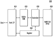
도 6은 앞서 설명된 다양한 실시예들에 따라 프로그램 동작을 수행하는 퓨전 메모리 장치 또는 퓨전 메모리 시스템을 간략히 보여주는 블록도이다. 예를 들면, 퓨전 메모리 장치로서 원낸드 플래시 메모리 장치(600)에 본 발명의 기술적 특징이 적용될 수 있다.6 is a block diagram schematically illustrating a fusion memory device or a fusion memory system performing a program operation according to various embodiments described above. For example, the technical features of the present invention may be applied to the one NAND
원낸드 플래시 메모리 장치(600)는 서로 다른 프로토콜을 사용하는 장치와의 각종 정보 교환을 위한 호스트 인터페이스(610)와, 메모리 장치를 구동하기 위한 코드를 내장하거나 데이터를 일시적으로 저장하는 버퍼 램(620)과, 외부에서 주어지는 제어 신호와 명령어에 응답하여 읽기와 프로그램 및 모든 상태를 제어하는 제어부(630)와, 명령어와 어드레스, 메모리 장치 내부의 시스템 동작 환경을 정의하는 설정(Configuration) 등의 데이터가 저장되는 레지스터(640) 및 불휘발성 메모리 셀과 페이지 버퍼를 포함하는 동작 회로로 구성된 낸드 플래시 셀 어레이(650)를 포함한다. 낸드 플래시 셀 어레이(650)의 메모리 어레이는 도 2에 도시된 메모리 어레이가 적용된다. The one NAND
도 7에는 본 발명에 따른 플래시 메모리 장치(712)를 포함한 컴퓨팅 시스템이 개략적으로 도시되어 있다.7 schematically illustrates a computing system including a
본 발명에 따른 컴퓨팅 시스템(700)은 시스템 버스(760)에 전기적으로 연결된 마이크로프로세서(720), 램(730), 사용자 인터페이스(740), 베이스밴드 칩셋(Baseband chipset)과 같은 모뎀(750) 및 메모리 시스템(710)을 포함한다. 본 발명에 따른 컴퓨팅 시스템(700)이 모바일 장치인 경우, 컴퓨팅 시스템(700)의 동작 전압을 공급하기 위한 배터리(미도시됨)가 추가적으로 제공될 것이다. 비록 도면에는 도시되지 않았지만, 본 발명에 따른 컴퓨팅 시스템(700)에는 응용 칩셋(Application chipset), 카메라 이미지 프로세서(Camera Image Processor: CIS), 모바일 디램, 등이 더 제공될 수 있음은 이 분야의 통상적인 지식을 습득한 자들에게 자명하다. 메모리 시스템(710)은, 예를 들면, 데이터를 저장하는 데 불휘발성 메모리를 사용하는 SSD(Solid State Drive/Disk)를 구성할 수 있다. 또는, 메모리 시스템(710)은, 퓨전 플래시 메모리(예를 들면, 원낸드 플래시 메모리)로 제공될 수 있다.
110 : 메모리 어레이 110MB : 메모리 블록
ST : 스트링 PAGE : 페이지
120 : 제어 회로 130 : 전압 공급 회로
131 : 전압 생성 회로 133 : 로우 디코더
140 : 페이지 버퍼 그룹 PB0~PBk : 페이지 버퍼
150 : 컬럼 선택 회로 160 : 입출력 회로
121 : 테스트 리드동작 제어부 123, 125, 127 : 레지스터110:
ST: String PAGE: Page
120: control circuit 130: voltage supply circuit
131: voltage generation circuit 133: low decoder
140: page buffer group PB0 to PBk: page buffer
150: column selection circuit 160: input / output circuit
121: test lead
Claims (20)
상기 메모리 셀들로부터 독출되는 데이터에 포함된 에러 비트의 수가 허용 범위를 벗어나면 상기 리드 전압의 인가 조건에 따라 상기 리드 전압의 레벨을 변경하면서 상기 리드 동작을 반복 실시하는 단계; 및
상기 에러 비트의 수가 허용 범위에 해당하면 상기 리드 동작이 실시된 횟수를 상기 내부 레지스터에 저장되는 단계를 포함하는 반도체 장치의 동작 방법.
Storing an application condition of a read voltage input from the outside of the chip in an internal register for a read operation of the memory cells;
Repeating the read operation while changing the level of the read voltage according to the application condition of the read voltage when the number of error bits included in the data read from the memory cells is out of an allowable range; And
And storing the number of times the read operation is performed in the internal register when the number of error bits corresponds to an allowable range.
상기 리드 동작은 테스트 모드에서 실시되는 반도체 장치의 동작 방법.
The method of claim 1,
And the read operation is performed in a test mode.
상기 데이터에 포함된 상기 에러 비트의 수를 확인하기 위하여 상기 데이터와 기준 데이터를 비교하는 단계를 더 포함하는 반도체 장치의 동작 방법.
The method of claim 1,
And comparing the data with reference data to identify the number of error bits included in the data.
상기 리드 전압의 인가 조건이 상기 내부 레지스터에 저장될 때 상기 기준 데이터도 상기 내부 레지스터에 저장되는 반도체 장치의 동작 방법.
The method of claim 3, wherein
And the reference data is stored in the internal register when the condition for applying the read voltage is stored in the internal register.
상기 리드 전압의 인가 조건이 상기 내부 레지스터에 저장될 때 상기 메모리 셀들을 선택하기 위한 어드레스 신호도 상기 내부 레지스터에 저장되는 반도체 장치의 동작 방법.
The method of claim 1,
And an address signal for selecting the memory cells is also stored in the internal register when the condition for applying the read voltage is stored in the internal register.
상기 내부 레지스터에 저장된 상기 리드 동작의 실시 횟수가 상기 칩의 외부로 출력되는 단계를 포함하는 반도체 장치의 동작 방법.
The method of claim 1,
And outputting the number of times of the read operation stored in the internal register to the outside of the chip.
상기 테스트 모드가 종료된 후 상기 내부 레지스터에는 상기 메모리 셀들의 프로그램 동작, 리드 동작 또는 소거 동작을 위한 전압들의 인가 조건이 저장되는 반도체 장치의 동작 방법.
The method of claim 1,
And a condition for applying voltages for program operation, read operation, or erase operation of the memory cells is stored in the internal register after the test mode ends.
상기 리드 전압의 인가 조건은 테스트 모드에서 호스트로부터 직접 입력되는 반도체 장치의 동작 방법.
The method of claim 1,
And a condition for applying the read voltage is input directly from a host in a test mode.
상기 리드 전압의 인가 조건은 상기 리드 전압의 최저 레벨, 상기 리드 전압의 최고 레벨, 상기 리드 전압의 변경 레벨 및 상기 리드 동작의 최대 허용 실시 횟수를 포함하는 반도체 장치의 동작 방법.
The method of claim 1,
And a condition for applying the read voltage includes a minimum level of the read voltage, a maximum level of the read voltage, a change level of the read voltage, and a maximum allowable number of times of the read operation.
테스트 리드 명령 신호가 입력되면 상기 칩의 내부에서 상기 리드 동작이 상기 리드 전압의 인가 조건에 따라 반복 실시되는 반도체 장치의 동작 방법.
The method of claim 1,
And a read operation is repeatedly performed in the chip according to a condition of applying the read voltage when a test read command signal is input.
상기 메모리 셀들의 리드 동작을 수행하도록 구성된 동작 회로; 및
상기 메모리 셀들의 리드 동작을 위하여 칩의 외부로부터 입력된 리드 전압의 인가 조건과 상기 리드 동작의 실시 횟수를 저장하기 위한 내부 레지스터를 포함하고, 상기 메모리 셀들로부터 독출되는 데이터에 포함된 에러 비트의 수가 허용 범위를 벗어나면 상기 리드 전압의 인가 조건에 따라 상기 리드 전압의 레벨을 변경하면서 상기 리드 동작이 반복 실시되도록 상기 동작 회로를 제어하는 제어 회로를 포함하는 반도체 장치.
A memory array including memory cells;
Operating circuitry configured to perform a read operation of the memory cells; And
An internal register for storing a read condition applied to the read voltage input from the outside of the chip and the number of times of the read operation for the read operation of the memory cells, and the number of error bits included in the data read from the memory cells. And a control circuit for controlling the operation circuit so that the read operation is repeatedly performed while changing the level of the read voltage in accordance with the application condition of the read voltage when outside the allowable range.
상기 제어 회로는 테스트 모드에서 상기 리드 전압의 레벨을 변경하면서 상기 리드 동작이 반복 실시되도록 상기 동작 회로를 제어하는 반도체 장치.
The method of claim 11,
And the control circuit controls the operation circuit so that the read operation is repeatedly performed while changing the level of the read voltage in a test mode.
상기 제어 회로는 상기 데이터에 포함된 상기 에러 비트의 수를 확인하기 위하여 상기 데이터와 기준 데이터를 비교하는 동작을 수행하도록 구성되는 반도체 장치.
The method of claim 11,
And the control circuit is configured to perform an operation of comparing the data with reference data to confirm the number of the error bits included in the data.
상기 리드 전압의 인가 조건이 상기 내부 레지스터에 저장될 때 상기 기준 데이터가 상기 내부 레지스터에 저장되는 반도체 장치.
14. The method of claim 13,
And the reference data is stored in the internal register when the condition for applying the read voltage is stored in the internal register.
상기 리드 전압의 인가 조건이 상기 내부 레지스터에 저장될 때 상기 메모리 셀들을 선택하기 위한 어드레스 신호도 상기 내부 레지스터에 저장되는 반도체 장치.
The method of claim 11,
And an address signal for selecting the memory cells is also stored in the internal register when the condition for applying the read voltage is stored in the internal register.
상기 내부 레지스터에 저장된 상기 리드 동작의 실시 횟수가 상기 동작 회로의 입출력 회로를 통해 상기 칩의 외부로 출력되는 단계를 포함하는 반도체 장치.
The method of claim 11,
And outputting the number of times of the read operation stored in the internal register to the outside of the chip through an input / output circuit of the operation circuit.
상기 테스트 모드가 종료된 후 상기 내부 레지스터는 상기 메모리 셀들의 프로그램 동작, 리드 동작 또는 소거 동작을 위한 전압들의 인가 조건을 저장하기 위해 사용되는 반도체 장치.
The method of claim 11,
And the internal register is used to store conditions for applying voltages for a program operation, a read operation, or an erase operation of the memory cells after the test mode ends.
상기 리드 전압의 인가 조건은 테스트 모드에서 호스트로부터 직접 입력되는 반도체 장치.
The method of claim 11,
And a condition for applying the read voltage is directly input from a host in a test mode.
상기 리드 전압의 인가 조건은 상기 리드 전압의 최저 레벨, 상기 리드 전압의 최고 레벨, 상기 리드 전압의 변경 레벨 및 상기 리드 동작의 최대 허용 실시 횟수를 포함하는 반도체 장치.
The method of claim 11,
The condition for applying the read voltage includes a minimum level of the read voltage, a maximum level of the read voltage, a change level of the read voltage, and a maximum allowable number of times of the read operation.
테스트 리드 명령 신호가 입력되면 상기 칩의 내부에서 상기 제어 회로의 제어에 의해 상기 동작 회로가 상기 리드 전압의 인가 조건에 따라 상기 리드 동작을 반복 실시하는 반도체 장치. The method of claim 11,
And a test read command signal is inputted in the chip, and the operation circuit repeatedly performs the read operation in accordance with a condition of applying the read voltage within the chip under control of the control circuit.
Priority Applications (2)
| Application Number | Priority Date | Filing Date | Title |
|---|---|---|---|
| KR1020120094349A KR20140029582A (en) | 2012-08-28 | 2012-08-28 | Semiconductor device and method of operating the same |
| US13/717,385 US9030873B2 (en) | 2012-08-28 | 2012-12-17 | Semiconductor device and method of operating the same |
Applications Claiming Priority (1)
| Application Number | Priority Date | Filing Date | Title |
|---|---|---|---|
| KR1020120094349A KR20140029582A (en) | 2012-08-28 | 2012-08-28 | Semiconductor device and method of operating the same |
Publications (1)
| Publication Number | Publication Date |
|---|---|
| KR20140029582A true KR20140029582A (en) | 2014-03-11 |
Family
ID=50187433
Family Applications (1)
| Application Number | Title | Priority Date | Filing Date |
|---|---|---|---|
| KR1020120094349A KR20140029582A (en) | 2012-08-28 | 2012-08-28 | Semiconductor device and method of operating the same |
Country Status (2)
| Country | Link |
|---|---|
| US (1) | US9030873B2 (en) |
| KR (1) | KR20140029582A (en) |
Cited By (1)
| Publication number | Priority date | Publication date | Assignee | Title |
|---|---|---|---|---|
| KR20170092176A (en) * | 2016-02-02 | 2017-08-11 | 에스케이하이닉스 주식회사 | Data storage device and operating method thereof |
Families Citing this family (8)
| Publication number | Priority date | Publication date | Assignee | Title |
|---|---|---|---|---|
| US10319460B2 (en) * | 2013-08-14 | 2019-06-11 | Infineon Technologies Ag | Systems and methods utilizing a flexible read reference for a dynamic read window |
| CN105489247B (en) * | 2014-09-16 | 2019-02-05 | 北京兆易创新科技股份有限公司 | A kind of test method and device of memory chip |
| KR102178538B1 (en) | 2014-12-16 | 2020-11-13 | 삼성전자주식회사 | Memory device, method of generating log of command signal/address signal of memory device, and method of analyzing error of memory device |
| KR102381218B1 (en) * | 2015-09-25 | 2022-04-01 | 에스케이하이닉스 주식회사 | Data storage device and operating method thereof |
| KR20180025357A (en) * | 2016-08-29 | 2018-03-09 | 에스케이하이닉스 주식회사 | Data storage device and operating method thereof |
| KR20180100984A (en) * | 2017-03-03 | 2018-09-12 | 에스케이하이닉스 주식회사 | Memory system and operating method of memory system |
| KR20200065298A (en) * | 2018-11-30 | 2020-06-09 | 에스케이하이닉스 주식회사 | Memory system and operating method thereof |
| KR102620262B1 (en) * | 2019-06-04 | 2024-01-03 | 에스케이하이닉스 주식회사 | Semiconductor memory device, operating methods thereof and memory system |
Family Cites Families (6)
| Publication number | Priority date | Publication date | Assignee | Title |
|---|---|---|---|---|
| US7954037B2 (en) * | 2005-10-25 | 2011-05-31 | Sandisk Il Ltd | Method for recovering from errors in flash memory |
| KR101578511B1 (en) | 2009-05-20 | 2015-12-18 | 삼성전자주식회사 | Method for setting a read voltage |
| KR20120109848A (en) * | 2011-03-28 | 2012-10-09 | 에스케이하이닉스 주식회사 | Semiconductor memory system and method for reading data of the same |
| US8510636B2 (en) * | 2011-04-01 | 2013-08-13 | Intel Corporation | Dynamic read channel calibration for non-volatile memory devices |
| US9047210B2 (en) * | 2011-09-15 | 2015-06-02 | Sandisk Technologies Inc. | Data storage device and method to correct bit values using multiple read voltages |
| US8793558B2 (en) * | 2012-08-27 | 2014-07-29 | Freescale Semiconductor, Inc. | Adaptive error correction for non-volatile memories |
-
2012
- 2012-08-28 KR KR1020120094349A patent/KR20140029582A/en not_active Application Discontinuation
- 2012-12-17 US US13/717,385 patent/US9030873B2/en active Active
Cited By (1)
| Publication number | Priority date | Publication date | Assignee | Title |
|---|---|---|---|---|
| KR20170092176A (en) * | 2016-02-02 | 2017-08-11 | 에스케이하이닉스 주식회사 | Data storage device and operating method thereof |
Also Published As
| Publication number | Publication date |
|---|---|
| US20140063971A1 (en) | 2014-03-06 |
| US9030873B2 (en) | 2015-05-12 |
Similar Documents
| Publication | Publication Date | Title |
|---|---|---|
| KR102016036B1 (en) | Semiconductor memory device and method of operating the same | |
| US9030873B2 (en) | Semiconductor device and method of operating the same | |
| US9466381B2 (en) | Semiconductor device | |
| US9318203B2 (en) | Semiconductor device being capable of improving program speed and program disturbance characteristics | |
| US9466389B2 (en) | Multiple programming pulse per loop programming and verification method for non-volatile memory devices | |
| KR20140020628A (en) | Semiconductor memory device | |
| US9543031B2 (en) | Semiconductor device to improve reliability of read operation for memory cells | |
| KR20130087857A (en) | Semiconductor memory device and method of operating the same | |
| KR20130027686A (en) | Semiconductor memory device and method of operating the same | |
| US20140185381A1 (en) | Semiconductor apparatus and method of operating the same | |
| KR20140134797A (en) | Semiconductor apparatus and method of operating the same | |
| US9036418B2 (en) | Read voltage generation circuit, memory and memory system including the same | |
| US9269443B2 (en) | Semiconductor device and program fail cells | |
| KR20140057901A (en) | Semiconductor memory device and operating method thereof | |
| CN105321574B (en) | Semiconductor device with a plurality of transistors | |
| KR20140079913A (en) | Nonvolatile memory device and programming method thereof | |
| US20150370481A1 (en) | Semiconductor device | |
| US20150194220A1 (en) | Semiconductor device and memory system including the same | |
| KR20140021909A (en) | Semiconductor memory device and operating method thereof | |
| KR20140028718A (en) | Semiconductor memory device and method of operating the same | |
| KR102039431B1 (en) | Semiconductor memory device and method of operating the same | |
| KR20140088383A (en) | Semiconductor apparatus and method of operating the same | |
| US9412452B2 (en) | Semiconductor device | |
| KR20140079912A (en) | Semiconductor memory device and operating method thereof | |
| US20160217859A1 (en) | Semiconductor device |
Legal Events
| Date | Code | Title | Description |
|---|---|---|---|
| WITN | Application deemed withdrawn, e.g. because no request for examination was filed or no examination fee was paid |