KR20140016150A - A printed circuit board and a method for manufacturing - Google Patents
A printed circuit board and a method for manufacturing Download PDFInfo
- Publication number
- KR20140016150A KR20140016150A KR1020130061168A KR20130061168A KR20140016150A KR 20140016150 A KR20140016150 A KR 20140016150A KR 1020130061168 A KR1020130061168 A KR 1020130061168A KR 20130061168 A KR20130061168 A KR 20130061168A KR 20140016150 A KR20140016150 A KR 20140016150A
- Authority
- KR
- South Korea
- Prior art keywords
- core
- layer
- circuit board
- printed circuit
- insulating layer
- Prior art date
Links
Images


Classifications
-
- H—ELECTRICITY
- H05—ELECTRIC TECHNIQUES NOT OTHERWISE PROVIDED FOR
- H05K—PRINTED CIRCUITS; CASINGS OR CONSTRUCTIONAL DETAILS OF ELECTRIC APPARATUS; MANUFACTURE OF ASSEMBLAGES OF ELECTRICAL COMPONENTS
- H05K1/00—Printed circuits
- H05K1/02—Details
- H05K1/03—Use of materials for the substrate
-
- H—ELECTRICITY
- H05—ELECTRIC TECHNIQUES NOT OTHERWISE PROVIDED FOR
- H05K—PRINTED CIRCUITS; CASINGS OR CONSTRUCTIONAL DETAILS OF ELECTRIC APPARATUS; MANUFACTURE OF ASSEMBLAGES OF ELECTRICAL COMPONENTS
- H05K3/00—Apparatus or processes for manufacturing printed circuits
- H05K3/40—Forming printed elements for providing electric connections to or between printed circuits
Abstract
Description
본 발명은 인쇄회로기판 및 그 제조방법에 관한 것이다.
The present invention relates to a printed circuit board and a manufacturing method thereof.
최근에 이르러 휴대용 기기들의 두께가 점점 얇아짐에 따라 내부에 장착되는 전자부품이 박형화와 함께 다수의 전자부품이 실장되는 기판도 박판으로 제작되어 전체적인 내부 부품들의 두께를 낮추려는 노력이 진행되고 있다.In recent years, as the thickness of portable devices becomes thinner and thinner, the electronic components mounted therein become thinner and the boards on which a plurality of electronic components are mounted are also made of thin plates, and efforts are being made to reduce the thickness of the entire internal components.
특히, 다수의 전자부품이 실장되는 기판은 박판으로 제작될 경우, 기판의 제조 공정 또는 전자부품의 실장 시에 리플로우 공정 등을 거치면서 고온에 노출되고, 고온 가공과 냉각을 반복하면서 재질의 특성에 의해 휨이 발생되는 문제점이 있다.In particular, when the board on which a large number of electronic components are mounted is manufactured in a thin plate, the substrate is exposed to high temperature through a reflow process during the manufacturing process of the board or the mounting of the electronic component, and the characteristics of the material while repeating high temperature processing and cooling There is a problem that warpage occurs by.
이러한 기판의 휨을 방지하기 위하여 기판의 제조 공정중에 사용되는 원자재의 강성을 높이고, 리플로우 공정시 열팽창계수(CTE) 차이에 의한 휨이 개선되도록 원자재의 열팽창계수 차이를 줄이기 위한 노력을 하고 있으나, 이에 대한 기술 개발이 더 필요한 실정이다.Efforts have been made to increase the rigidity of the raw materials used during the manufacturing process of the substrate in order to prevent the warpage of the substrate, and to reduce the thermal expansion coefficient difference of the raw materials to improve the warpage caused by the difference in the thermal expansion coefficient (CTE) during the reflow process. More technical development is needed.
또한, 기판의 제조 공정 중에 물리적인 구조 개선에 의해 휨을 방지하기 위한 방편으로 기판의 코어재에 대한 강성을 높이기 위하여 기판 내부에 금속성 보강재를 더 삽입하는 방법을 검토하고 있으나, 보강재가 금속 재질이기 때문에 회로 패턴을 전기적으로 연결하기 위한 비아 등을 형성하기 위하여 금속 보강재의 특정 부분을 미리 제거해 놓아야 한다.In addition, to improve the rigidity of the core material of the substrate as a way to prevent warpage by improving the physical structure during the manufacturing process of the substrate, a method of further inserting a metallic reinforcement inside the substrate is considered, but since the reinforcement is a metal material Certain portions of the metal reinforcement must be removed in advance to form vias or the like for electrically connecting the circuit pattern.
그러나, 금속 보강재 또는 금속 코어재에 비아 등을 형성하기 위해서는 에칭 공정 또는 레이져를 이용하여 금속 보강재를 제거하는 데, 금속 보강재의 가공을 위하여 별도의 캐리어를 구비하고, 캐리어 상의 금속 보강재 상에 절연층을 형성한 후 캐리어를 제거하는 공정을 거쳐야 하기 때문에 기판의 제조 비용이 증가하는 문제점이 지적되고 있다However, in order to form a via or the like in the metal reinforcement or the metal core material, the metal reinforcement is removed by using an etching process or a laser, and a separate carrier is provided for processing the metal reinforcement, and an insulating layer is formed on the metal reinforcement on the carrier. The problem of increasing the manufacturing cost of the substrate has been pointed out because it has to go through the process of removing the carrier after forming the
또한, 종래의 금속 보강재를 사용하는 경우에는 관통홀이 금속 보강재와 접촉하지 않도록 관통홀이 지나갈 위치에 금속 보강재의 일부를 미리 제거한 후, 관통홀을 포함한 표면에 절연층을 도포해야 함에 따라 회로 배선의 형성시 파인 피치(fine pitch)의 관통홀을 형성하기가 어려운 단점이 있다.
In the case of using a conventional metal reinforcing material, a part of the metal reinforcing material must be removed beforehand so that the through hole does not come into contact with the metal reinforcing material, and then an insulating layer must be applied to the surface including the through hole. There is a disadvantage in that it is difficult to form a fine pitch through hole at the time of formation.
본 발명의 일 목적은, 휨 발생이 방지되는 인쇄회로기판을 제공하기 위한 것이다.One object of the present invention is to provide a printed circuit board in which warpage is prevented.
본 발명의 일 목적은, 인쇄회로기판의 제조 공정 중에 기판의 휨 발생을 최소화할 수 있는 인쇄회로기판의 제조방법을 제공하는 것이다.
An object of the present invention is to provide a method for manufacturing a printed circuit board which can minimize the occurrence of warpage of the substrate during the manufacturing process of the printed circuit board.
본 발명의 상기 목적은, 절연층과 코어 보강재가 교호로 적층된 코어를 포함하는 인쇄회로기판이 제공됨에 의해서 달성된다.The above object of the present invention is achieved by providing a printed circuit board comprising a core in which an insulating layer and a core reinforcement are laminated alternately.
이때, 상기 코어는 상기 절연층 사이에 상기 코어 보강재가 개재된 구성이거나, 상기 절연층 양면에 상기 코어 보강재가 적층된 구성일 수 있다.In this case, the core may have a configuration in which the core reinforcing material is interposed between the insulating layers, or the core reinforcing material is laminated on both surfaces of the insulating layer.
또한, 상기 코어 보강재는 판 상의 글라스 재질 또는 비전기전도성 고분자 재질의 필름 형태로 구성될 수 있다.In addition, the core reinforcing material may be configured in the form of a film of glass or non-conductive polymer material on the plate.
상기 코어 보강재는 상기 코어의 전체 두께에 대한 상기 코어 보강재 두께의 비율이 35% 내지 80%의 범위를 가지며, 상기 코어는 상기 코어 보강재와 절연층의 열팽창계수(CTE)와 열팽창률의 관계에서 휨 특성에 대하여 하기의 수학식을 만족할 수 있다.The core stiffener has a ratio of the core stiffener thickness to the total thickness of the core in the range of 35% to 80%, the core is warped in the relationship between the coefficient of thermal expansion (CTE) and the thermal expansion coefficient of the core stiffener and the insulating layer The following equations may be satisfied with respect to the characteristics.
수학식Equation

α1 : 코어 보강재의 열팽창계수(1/k),α 1 : coefficient of thermal expansion of the core reinforcement (1 / k),
α2 : 절연층의 열팽창계수(1/k)이고,α 2 is the coefficient of thermal expansion of the insulating layer (1 / k),
E1 : 코어 보강재의 열팽창률(GPa)이고,E 1 is the coefficient of thermal expansion (GPa) of the core reinforcing material,
E2 : 절연재의 열팽창률(GPa)이다.E 2 : Thermal expansion coefficient (GPa) of the insulating material.
한편, 본 발명의 다른 목적은, 강성이 구비된 코어 보강재; 상기 코어 보강재의 양면에 형성된 절연층; 상기 절연층과 코어 보강재를 관통하여 형성된 관통홀; 및 상기 절연층 상에 형성된 회로층과 상기 회로층의 층간 연결을 위하여 상기 관통홀에 형성된 도금층;을 포함하는 인쇄회로기판이 제공됨에 의해서 달성될 수 있다.On the other hand, another object of the present invention, the core reinforcing material provided with rigidity; Insulating layers formed on both surfaces of the core reinforcing material; A through hole formed through the insulating layer and the core reinforcement material; And a plating layer formed in the through hole for connecting the circuit layer formed on the insulating layer and the layer of the circuit layer.
그리고, 본 발명의 목적은 코어 보강재를 준비하는 단계; 상기 코어 보강재의 양면에 절연층을 형성하는 단계; 상기 코어 보강재와 절연층을 관통하는 관통홀을 형성하는 단계; 및 상기 관통홀의 내부에 도금층을 형성함과 아울러 상기 절연층의 표면에 회로층을 형성하는 단계; 를 포함하는 인쇄회로기판의 제조방법이 제공됨에 의해서 달성된다.And, the object of the present invention is to prepare a core reinforcement; Forming insulating layers on both sides of the core reinforcing material; Forming a through hole penetrating the core reinforcing material and the insulating layer; And forming a plating layer inside the through hole and forming a circuit layer on the surface of the insulating layer. It is achieved by providing a method for manufacturing a printed circuit board comprising a.
또한, 본 발명의 또 다른 목적은, 절연층; 상기 절연층의 양면에 적층된 코어 보강재; 상기 절연층과 코어 보강재를 관통하여 형성된 관통홀; 및 상기 코어 보강재 상에 형성된 회로층;을 포함하는 인쇄회로기판이 제공됨에 의해서 달성된다.In addition, another object of the present invention, the insulating layer; A core reinforcing material laminated on both sides of the insulating layer; A through hole formed through the insulating layer and the core reinforcement material; And a circuit layer formed on the core reinforcing material.
그리고, 본 발명의 목적은 절연층의 양면에 코어 보강재를 접합하는 단계; 상기 코어 보강재 상에 시드층을 형성하는 단계; 상기 시드층 상에 회로 형성용 개구부를 갖는 도금 레지스트층을 형성하는 단계; 상기 회로 형성용 개구부에 도금층을 형성하는 단계; 및 상기 도금 레지스트층을 제거하여 회로층을 형성하는 단계;를 포함하는 인쇄회로기판의 제조방법이 제공됨에 의해서 달성된다.
And, the object of the present invention is the step of bonding the core reinforcing material on both sides of the insulating layer; Forming a seed layer on the core stiffener; Forming a plating resist layer having an opening for forming a circuit on the seed layer; Forming a plating layer in the opening for forming the circuit; And removing the plating resist layer to form a circuit layer, which is achieved by providing a method of manufacturing a printed circuit board.
이상에서 설명한 바와 같이, 본 발명에 따른 인쇄회로기판 및 그 제조방법은 강성을 가진 글라스 또는 비전기전도성 고분자 재질로 필름 형태의 코어 보강재가 개재되어 제작됨에 의해서 고온에서 인쇄회로기판의 강성이 유지됨에 따라 제작 공정 중의 휨을 방지할 수 있는 장점이 있다.As described above, the printed circuit board and the method of manufacturing the same according to the present invention are made of glass or non-conductive polymer material having rigidity, and the rigidity of the printed circuit board is maintained at a high temperature by interposing a film reinforcement material. Therefore, there is an advantage that can be prevented during the manufacturing process.
또한, 본 발명은 박판의 인쇄회로기판이 제작되어도 코어 보강재의 강성이 유지되기 때문에 처짐을 개선할 수 있으며, 수직 방향의 방열 특성을 향상시킬 수 있는 이점이 있다.
In addition, the present invention can improve the deflection because the rigidity of the core reinforcing material is maintained even if a thin printed circuit board is manufactured, there is an advantage that can improve the heat radiation characteristics in the vertical direction.
도 1은 본 발명에 따른 인쇄회로기판의 제1 실시예 단면도.
도 2 내지 도 5는 제1 실시예에 따른 인쇄회로기판의 제조방법이 도시된 공정 단면도로서,
도 2는 코어 보강재의 단면도이고,
도 3a는 코어 보강재에 절연층이 적층된 단면도이고,
도 3b는 코어 보강재와 절연층 사이에 코팅층이 개재된 단면도이고,
도 3c는 절연층 상에 금속 박막이 형성된 단면도이고,
도 4는 관통홀이 형성된 단면도이고,
도 5는 절연층에 회로층이 형성되고, 관통홀 내에 도금층이 형성된 단면도이다.
도 6은 본 발명에 따른 인쇄회로기판의 제2 실시예 단면도.
도 7 내지 도12는 제2 실시예에 따른 인쇄회로기판의 제조방법이 도시된 공정 단면도로서,
도 7은 절연층에 코어 보강재가 적층된 단면도이고,
도 8은 관통홀이 형성된 단면도이고,
도 9는 코어 보강재 표면과 관통홀 내벽에 시드층이 형성된 단면도이고,
도 10은 도금 레지스트층이 형성된 단면도이고,
도 11은 도금층이 형성된 단면도이고,
도 12는 회로층이 형성된 단면도이다.
도 13은 본 발명의 일실시예에 따른 인쇄회로기판에 복수의 절연층과 회로층이 빌드업된 다층 인쇄회로기판의 단면도.
도 14는 본 발명에 따른 제1 실시예의 인쇄회로기판과 종래 기술에 따른 인쇄회로기판의 휨 특성 시뮬레이션 그래프
도 15는 본 발명에 따른 제1 실시예와 제2 실시예의 인쇄회로기판에 대한 강성 특성 시뮬레이션 그래프.
도 16은 본 발명에 따른 제1 실시예와 제2 실시예의 인쇄회로기판에 대한 휨 특성 시뮬레이션 그래프.1 is a cross-sectional view of a first embodiment of a printed circuit board according to the present invention;
2 to 5 are cross-sectional views illustrating a method of manufacturing a printed circuit board according to the first embodiment.
2 is a cross-sectional view of the core reinforcement,
3A is a cross-sectional view of an insulation layer laminated on a core reinforcement material;
3B is a cross-sectional view with a coating interposed between the core reinforcing material and the insulating layer,
3C is a cross-sectional view of a metal thin film formed on an insulating layer;
4 is a cross-sectional view of the through-hole is formed,
5 is a cross-sectional view in which a circuit layer is formed in an insulating layer and a plating layer is formed in a through hole.
6 is a sectional view of a second embodiment of a printed circuit board according to the present invention;
7 to 12 are cross-sectional views illustrating a method of manufacturing a printed circuit board according to the second embodiment.
7 is a cross-sectional view of the core reinforcing material laminated on the insulating layer,
8 is a cross-sectional view of the through-hole is formed,
9 is a sectional view in which a seed layer is formed on the surface of the core reinforcement and the inner wall of the through hole,
10 is a sectional view in which a plating resist layer is formed,
11 is a cross-sectional view of the plating layer is formed,
12 is a cross-sectional view in which a circuit layer is formed.
13 is a cross-sectional view of a multilayer printed circuit board having a plurality of insulating layers and circuit layers built up on the printed circuit board according to an embodiment of the present invention.
14 is a simulation graph of the bending characteristics of a printed circuit board according to the first embodiment of the present invention and a conventional printed circuit board.
15 is a stiffness characteristic simulation graph for the printed circuit board of the first embodiment and the second embodiment according to the present invention;
16 is a bending characteristic simulation graph of the printed circuit board of the first embodiment and the second embodiment according to the present invention.
본 발명에 따른 인쇄회로기판 및 그 제조방법의 상기 목적에 대한 기술적 구성을 비롯한 작용효과에 관한 사항은 본 발명의 바람직한 실시예가 도시된 도면을 참조한 아래의 상세한 설명에 의해서 명확하게 이해될 것이다.Matters relating to the operational effects including the technical configuration of the printed circuit board and the manufacturing method according to the present invention will be clearly understood by the following detailed description with reference to the drawings showing preferred embodiments of the present invention.
또한, 본 발명을 설명함에 있어서, 관련된 공지 기술에 대한 구체적인 설명이 본 발명의 요지를 불필요하게 흐릴 수 있다고 판단되는 경우 그 상세한 설명은 생략한다. 본 명세서에서 제1, 제2 등의 용어는 하나의 구성요소를 다른 구성요소로부터 구별하기 위해 사용되는 것으로 구성요소가 상기 용어들에 의해 제한되는 것은 아니다.
In the following description, well-known functions or constructions are not described in detail since they would obscure the invention in unnecessary detail. As used herein, the terms "first", "second", and the like are used to distinguish one component from another component, and a component is not limited by the terms.
제1 1st 실시예Example 인쇄회로기판 Printed circuit board
먼저, 도 1은 본 발명에 따른 인쇄회로기판의 제1 실시예 단면도이다.First, Figure 1 is a cross-sectional view of a first embodiment of a printed circuit board according to the present invention.
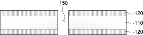
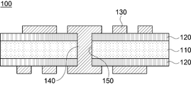
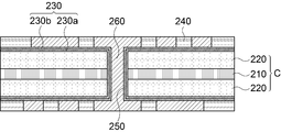
도 1에 도시된 바와 같이, 본 실시예에 따른 인쇄회로기판(100)은 코어 보강재(110)와, 코어 보강재(110)의 양면에 형성된 절연층(120)을 포함하는 코어(C) 및 상기 절연층(120) 상에 형성된 회로층(130)으로 구성될 수 있다.As shown in FIG. 1, the printed
이때, 상기 인쇄회로기판(100)은 코어 보강재(110)와 절연층(120)을 동시에 관통하는 관통홀(150)이 구비되며, 상기 절연층(120)의 상면과 상기 관통홀(150)의 내부에는 각각 회로층(130)과 도금층(140)이 형성될 수 있다.In this case, the printed
상기 코어 보강재(110)와 절연층(120) 사이에는 코어 보강재(110)의 표면에 절연층(120)의 밀착력을 강화하기 위한 코팅층(도면 미도시)이 더 형성될 수 있다. 코팅층은 코어 보강재(110) 표면에 플라즈마 처리에 의한 이온화 -OH기를 증가시켜 코어 보강재(110)와 절연층(120)의 밀착력이 증가되도록 할 수 있으며, 커플링 에이전트 등의 도포에 의해 형성되어 밀착력이 확보될 수 있도록 할 수 있다.A coating layer (not shown) may be further formed between the
이때, 상기 코팅층은 대략 2㎛ 이하의 두께로 형성됨이 바람직하다.At this time, the coating layer is preferably formed to a thickness of about 2㎛ or less.
여기서, 상기 코어 보강재(110)는 글라스(glass) 또는 비전기전도성 고분자 재질로 구성될 수 있다. 글라스는 판 형태의 글라스가 이용될 수 있으며, 인쇄회로기판의 전체적인 두께에 비례하여 약 25 내지 200㎛의 두께로 형성될 수 있다.Here, the
코어 보강재(110)로 이용되는 글라스의 두께를 25 내지 200㎛의 두께로 한정하는 이유는, 인쇄회로기판의 제조 공정 중에 소정의 휨이 가해질 수 있는 데, 글라스의 두께가 25 내지 200㎛에서 휨의 곡률 반경이 10㎝ 이하까지 파손되지 않고 견딜 수 있기 때문이다.The reason for limiting the thickness of the glass used as the
글라스가 코어 보강재(110)로 이용될 경우에 글라스는 0.6W/mK 내외의 열전도도를 가지는 글라스 재질을 적용하는 것이 바람직하며, 더 바람직하게는 국부적인 열적 스트레스(thermal stress)를 방지하기 위해 1.0W/mK 이상의 열전도도를 가지는 글라스 재질이 사용될 수 있다.When the glass is used as the
이와 같이, 글라스 재질을 코어 보강재(110)로 사용할 경우에는 글라스 재질이 50GPa 이상의 높은 강성(Elastic Module)을 가지고 있기 때문에 인쇄회로기판의 제조 공정시 발생되는 휨을 방지할 수 있다.As such, when the glass material is used as the
또한, 상기 코어 보강재(110)는 글라스 대신에 필름 형태의 비전기전도성 고분자 재질로 구성될 수도 있다.In addition, the
상기 코어 보강재(110)의 양면에 형성된 절연층(120)은 여러 가닥의 글라스 패브릭이 포함되어 코어 보강재(110)와 별도로 휨에 대응될 수 있는 강성이 유지되도록 할 수 있다.The insulating
이와 더불어, 상기 절연층(120)은 필름 타입 또는 글라스 패브릭이 포함된 절연 시트로 구성될 수 있다.In addition, the insulating
절연 시트로 절연층(120)이 구성될 경우에는 코어 보강재(110)의 양면에 각각 절연 시트를 라미네이션하고, 절연 시트의 상면을 열과 압력을 가하여 압착함에 의해서 코어 보강재(110) 표면에 절연 시트가 접합되도록 할 수 있다.When the insulating
상기 절연층(120)은 코어 보강재(110)의 양면에 형성되는 것으로 도시하고 이에 대하여 구체적으로 설명하였으나, 이에 한정되는 것은 아니고 코어 보강재(110)의 일면에만 형성될 수도 있다.The insulating
그리고, 상기 절연층(120)이 형성된 코어 보강재(110)는 절연층(120)과 코어 보강재(110)를 관통하는 관통홀(150)이 형성되는 데, 상기 관통홀(150)의 내부에는 도금층(140)이 형성되고, 절연층(120) 상에는 회로층(130)이 형성될 수 있다. 상기 회로층(130)과 도금층(140)은 전기 동도금에 의해 형성될 수 있으며, 절연층(120) 상에 형성된 회로층(130)은 회로 패턴을 구성하게 되고, 관통홀(150) 내부에 형성된 도금층(140)은 절연층(120) 상에 형성된 회로층(130)을 전기적으로 연결하는 층간 연결층으로 구성될 수 있다.In addition, the
또한, 상기 절연층(120) 상에는 2㎛ 이하의 얇은 금속 박막(도면 미도시)이 더 형성될 수 있다. 상기 금속 박막은 주로 동박으로 구성될 수 있으며, 코어 보강재(110)에 절연층(120)의 도포시 동시에 형성될 수 있다.In addition, a thin metal thin film (not shown) of 2 μm or less may be further formed on the insulating
상기 금속 박막은 회로층(130)의 형성을 위한 전기 동도금시 시드층으로 이용되는 데, 절연층(120)과 코어 보강층(110)을 관통홀(150)을 형성하기 위한 레이져 가공이 가능하도록 2㎛ 이하의 두께로 형성되어야 한다. 그리고, 상기 금속 박막은 전기 전도가 가능한 카본의 재질로 구성될 수도 있다.
The metal thin film is used as a seed layer during the electroplating process for forming the
제1 1st 실시예Example 인쇄회로기판의 제조방법 Manufacturing method of printed circuit board
한편, 아래 도시된 도 2 내지 도 5를 통해 본 실시예에 따른 인쇄회로기판의 제조방법을 살펴보면 다음과 같다.Meanwhile, the manufacturing method of the printed circuit board according to the present embodiment will be described with reference to FIGS. 2 to 5 as follows.
먼저, 도 2에 도시된 바와 같이 코어 보강재(110)를 준비한다. 코어 보강재(110)는 판형의 글라스 또는 비전기전도성 고분자 재질로 구성될 수 있으며, 비전기전도성 고분자 재질의 경우 필름 형태로 구성될 수 있다.First, as shown in FIG. 2, the
이때, 코어 보강재(110)는 글라스의 경우 50GPa 이상의 강성을 가지고 25 내지 200㎛의 두께로 형성됨이 바람직하며, 상기 두께가 유지될 때 인쇄회로기판의 제조 공정시 소정의 곡률 반경을 가지고 변형되었다가 파손없이 원상태로 복귀될 수 있다.In this case, the
다음, 도 3a에 도시된 바와 같이 코어 보강재(110)의 양면에 절연층(120)을 형성하여 코어(C)를 제작할 수 있다. 절연층(120)은 코어 보강재(110) 상에 절연 재질이 도포됨에 의해 형성되며, 글라스 패브릭 재질이 첨가된 절연재가 도포될 수도 있다.Next, as illustrated in FIG. 3A, the core C may be manufactured by forming the insulating
이때, 도 3b에 도시된 바와 같이 상기 절연층(120)을 형성하기 전에 코어 보강재(110)의 일면 또는 양면에는 코팅층(115)이 더 형성될 수 있다. 코팅층(115)은 코어 보강재(110)와 절연층(120)의 밀착력을 강화시키기 위한 얇은 절연층으로 주로 고분자 물질이 도포되어 절연층(120)의 접착 성능을 향상시킬 수 있다. 코팅층(115)은 2㎛ 내외로 형성됨이 바람직하며, 코어 보강재(110)의 표면에 플라즈마 처리에 의한 -OH기를 증가시켜 밀착력이 증대되도록 할 수 있다.In this case, as shown in FIG. 3B, the
또한, 상기 코팅층(115)은 코어 보강재(110)의 표면 플라즈마 처리 외에 커플링 에이전트 등을 코어 보강재(110)의 표면에 도포하여 형성되게 할 수 있다.In addition, the
다음으로, 도 4에 도시된 바와 같이 상기 코어 보강재(110)와 절연층(120)을 관통하는 관통홀(150)이 형성될 수 있다. 상기 관통홀(150)은 주로 레이져 가공을 통해 형성될 수 있으며, CO2 레이져를 이용하여 관통홀(150)이 가공될 수 있다. 상기 관통홀(150)은 절연 재질인 코어 보강재(110)와 절연층(120)이 레이져 조사에 의해 형성됨에 따라 관통홀(150) 내벽면에 종래와 같이 층간 도통이 방지되는 별도의 절연 기재를 형성할 필요가 없고, 레이져 가공만으로 관통홀 형성이 가능함에 따라 파인 피치(fine pitch)의 관통홀 가공이 가능할 수 있다.Next, as illustrated in FIG. 4, a through
한편, 상기 코어 보강재(110)와 절연층(120)에 관통홀을 형성하기 전에 도 3c에 도시된 바와 같이 상기 절연층(120) 상에 약 2㎛ 내외의 얇은 금속 박막(125)이 더 형성될 수 있다. 상기 금속 박막(125)은 주로 동박으로 구성될 수 있으며, 그 두께가 레이져 가공이 가능한 정도의 두께(5㎛ 이하의 두께에서 CO2레이져 가공 가능함)로 형성되기 때문에 소정의 위치에서 CO2 레이져를 조사하여 관통홀(150) 가공이 가능할 수 있다.Meanwhile, before forming the through hole in the
이때, 관통홀(150)이 형성된 부분 외의 절연층(120) 상에 형성된 금속 박막(125)은 이 후 공정에서 회로층 형성을 위한 동도금시 시드층으로 이용될 수 있다.In this case, the metal
다음으로, 도 5에 도시된 바와 같이 상기 관통홀(150)의 내부와 절연층(120)의 상면에 각각 도금층(140)과 회로층(130)이 형성될 수 있다. 상기 도금층(140)과 회로층(130) 중에 절연층(120) 상에 형성된 회로층(130)은 회로 패턴으로 구성될 수 있으며, 상기 관통홀(150) 내에 형성된 도금층(140)은 회로 패턴을 구성하는 절연층(120) 상의 회로층(130)을 전기적으로 연결하는 층간 연결층으로 이용될 수 있다.Next, as shown in FIG. 5, the
상기 회로층(130)과 도금층(140)은 전기 동도금에 의해 형성될 수 있으며, 절연층(120) 상면과 관통홀(150) 내부에 동시에 형성될 수 있다.
The
제2 Second 실시예Example 인쇄회로기판 Printed circuit board
한편, 도 6은 본 발명에 따른 인쇄회로기판의 제2 실시예 단면도이다.6 is a cross-sectional view of a second embodiment of a printed circuit board according to the present invention.
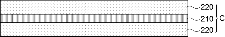
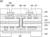
도시된 바와 같이, 본 실시예에 따른 인쇄회로기판(200)은 절연층(210)과, 절연층(210) 상에 형성된 코어 보강재(220)를 포함하는 코어(C) 및 상기 코어(C) 상에 형성된 회로층(270)을 포함하여 구성될 수 있다.As shown, the printed
이때, 절연층(210)은 앞서 설명한 제1 실시예의 인쇄회로기판에 적용된 절연층과 같이 여러 가닥의 글라스 패브릭이 포함된 절연재로 구성될 수 있으며, 필름 타입 또는 글라스 패브릭이 혼재된 절연 시트로 구성될 수도 있다.At this time, the insulating
도면에 도시된 바와 같이, 절연층(210)은 코어 보강재(220)의 양면에 부착될 수 있으나, 이는 하나의 실시예에 불과한 것이고, 절연층(210)의 일면에만 코어 보강재(220)가 부착될 수도 있다.As shown in the figure, the insulating
코어 보강재(220)는 대략 50Gpa 이상의 강성을 갖는 글라스가 적용될 수 있으며, 얇은 판상의 글라스가 절연층(210)의 상, 하면에 각각 적층될 수 있다. 이때, 코어 보강재(220)는 글라스 대신에 비전기전도성 고분자 재질로 구성될 수도 있다.The
이와 같이, 절연층(210)을 사이에 두고 절연층(210)의 양면에 판상의 글라스가 코어 보강재(220)로 채용되었을 때, 코어 보강재(220) 사이의 절연층(210)이 충격 흡수 역할을 하게 됨으로써, 인쇄회로기판의 제조 공정 중에 코어 보강재(220)가 파손되는 것을 방지할 수 있다.As such, when plate-shaped glass is employed as the
여기서, 코어 보강재(220) 사이에 적층된 절연층(210)이 하나의 층으로 이루어진 것으로 도시하고 있으나, 이는 일 실시예를 설명하기 위한 것이고, 두 개 이상의 다층으로 절연층을 형성하는 것도 가능할 수 있다.Here, although the insulating
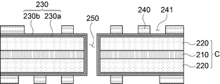
상기 회로층(270)은 코어 보강재(220) 상에 소정의 패턴으로 구성될 수 있는 바, 회로층(270)은 제1 실시예와 마찬가지로 코어 보강재(220)와 절연층(210)을 관통하여 형성된 관통홀(250)에 충진되어 있는 도금층(260)에 의해서 상기 코어 보강재(220) 상에 형성된 회로층(270)의 층간 연결이 이루어질 수 있다.The
회로층(270)은 코어 보강재(220) 상에서 도금층에 의해서 형성될 수 있으며, 회로층(270) 형성을 위한 도금층 형성시 시드층(230)을 먼저 형성한 후 도금층이 형성되고, 도금층의 패터닝에 의해서 회로층(270)이 형성될 수 있다. 이때, 시드층(230)은 제1 시드층(230a)과 제2 시드층(230b)으로 형성될 수 있다.The
제1 시드층(230a)과 제2 시드층(230b)을 포함하는 시드층(230)은 티타늄(Ti), 구리(Cu), 몰리브덴(Mo), 니켈(Ni), 은(Ag), 아연(Zn), 탄소(C) 등의 전도성 금속재 또는 이들의 합금으로 이루어진 군으로부터 선택된 어느 하나로 이루어질 수 있다.The
또한, 상기 시드층(230)과 회로층(270)은 비용적인 측면과 공정상 이점 등을 고려하여 구리(Cu)로 구성됨이 바람직하다.In addition, the
이와 같이 구성된 본 실시예의 인쇄회로기판(200)은 절연층(210)을 중심으로 한 코어 보강재(220)가 판상의 글라스로 구성되기 때문에 코어 보강재(220) 상에 형성된 회로층(270)이 매끄러운 표면에 형성됨으로써, 코어 보강재(220)와 회로층(270) 사이 계면에 러프니스(roughness)가 없어 신호의 잡음이 적고, 초미세 피치를 갖는 회로층(270) 구현이 용이할 수 있다.The printed
이는, 회로층(270)이 매끄러운 표면, 즉 표면 조도가 작기 때문에 회로층 형성을 위한 에칭량이 줄어들게 되고, 회로 형성시의 손실량을 줄여 초미세 피치 형성이 가능하고, 신호 잡음이 현저히 줄어들 수 있다.
Since the
제2 Second 실시예Example 인쇄회로기판의 제조방법 Manufacturing method of printed circuit board
다음, 도 7 내지 도 12는 본 발명에 따른 제2 실시예 인쇄회로기판 제조방법이 순차적으로 도시된 공정단면도이다.Next, FIGS. 7 to 12 are process cross-sectional views sequentially illustrating a method of manufacturing a printed circuit board according to a second embodiment of the present invention.
먼저, 도 7에 도시된 바와 같이 절연층(210)의 상, 하면에 코어 보강재(220)를 부착하여 코어(C)를 제작할 수 있다. 이때, 절연층(210)은 내열성을 갖는 고분자 재질로 글라스 패브릭이 함침된 절연재로 구성될 수 있으며, 필름 타입 또는 글라스 패브릭이 혼재된 절연 시트로 구성될 수도 있다. 또한, 상기 코어 보강재(220) 사이에 적층된 절연층(210)이 공정 중 발생되는 충격을 흡수함에 의해서 코어 보강재(220)가 충격 또는 휨에 의해 파손되는 것을 방지할 수 있다.First, as shown in FIG. 7, the core C may be manufactured by attaching the
상기 코어(C)를 제작하는 단계는 절연층(210)의 양면에 코어 보강재(220)를 적층하는 단계와, 코어 보강재(220)와 절연층(210)을 순차적으로 적층하고 가열, 가압하여 절연층(210) 양면에 코어 보강재(220)를 접합하는 단계를 더 포함할 수 있다.The manufacturing of the core C may include stacking the
다음, 도 8에 도시된 바와 같이 절연층(210)과 코어 보강재(220)가 적층된 코어(C)를 관통하는 관통홀(250)을 형성할 수 있다. 관통홀(250)은 레이져 드릴링에 의해 형성될 수 있으며, 대표적으로 CO2 레이져, YAG 레이져 또는 펄스 UV 엑시머 레이져 등이 적용될 수 있다.Next, as shown in FIG. 8, a through
한편, 코어(C)에 관통홀(250)을 형성하는 단계 이후에는 관통홀(250)을 형성한 코어(C)의 표면과 관통홀(250) 내벽을 클리닝하는 단계를 더 포함할 수 있다. 이때, 코어(C) 표면과 관통홀(250) 내벽의 클리닝 시 특별히 어느 한 공정에 한정되지는 않으나, 건식 에칭 또는 습식 에칭이 적용될 수 있고, 디스미어 공정에 의해 수행될 수 있다. 이 중에서 건식 에칭 공정은 플라즈마 에칭, 스퍼터 에칭 또는 이온 에칭 등이 이용될 수 있다.Meanwhile, after the forming of the through
다음으로, 도 9에 도시된 바와 같이 관통홀(250) 내벽을 포함한 코어(C)의 표면에 시드층(230)을 형성할 수 있다. 시드층(230)은 후속 공정에서 회로층(270) 형성을 위한 도금층 형성시 도금층 성장이 용이하게 하기 위함이며, 주로 스퍼터링 공법을 통해 형성될 수 있다. 그리고, 시드층(230)은 경우에 따라 제1 시드층(230a)과 제2 시드층(230b)으로 구분되어 형성될 수 있으며, 티타늄(Ti), 알루미늄(Al), 구리(Cu), 몰리브덴(Mo), 니켈(Ni), 은(Ag), 아연(Zn), 탄소(C) 또는 이들의 합금으로 이루어진 군으로부터 선택된 어느 하나로 이루어질 수 있다.Next, as illustrated in FIG. 9, the
이 후에, 도 10에 도시된 바와 같이 시드층(230) 상에 회로 형성용 개구부(241)를 갖는 도금 레지스트층(240)을 형성할 수 있다. 도금 레지스트층(240)은 감광성 폴리머를 이용한 포토 레지스트를 이용하여 형성될 수 있으며, 포토 레지스트의 도포 후 마스크를 이용하여 회로 형성용 개구부(241)를 형성할 수 있다. 이때, 도금 레지스트층(240)의 회로 형성용 개구부(241)는 회로 패턴 설계 사양에 따라 형성될 수 있다.Thereafter, as shown in FIG. 10, the plating resist
다음으로, 도 11과 도 12에 도시된 바와 같이 도금 레지스트층(240)이 형성된 코어 보강재(220) 상에 도금층(260)을 형성하고, 도금 레지스트층(240)을 제거하여 회로층(270)을 형성할 수 있다.Next, as shown in FIGS. 11 and 12, the
여기서, 상기 코어 보강재(220) 상에 도금층(260)을 형성하는 도금 공정은 전해 도금에 의해서 이루어질 수 있으며, 도금층(260) 구리(Cu)로 구성됨이 바람직하다. 그리고, 상기 도금 레지스트층(240)을 제거하는 단계에서는 기계적 박리 또는 화학 용액을 이용한 화학적 박리 공정을 통해 수행될 수 있다.
Here, the plating process of forming the
이와 같이 구성된 제1 실시예와 제2 실시예의 인쇄회로기판(100, 200)은 도 13에 도시된 바와 같이, 코어 보강재(220) 양면에 절연층(210)이 형성되거나, 절연층(210) 양면에 코어 보강재(220)가 적층된 구성의 코어(C)를 중심으로 그 상, 하면에 각각 제2 절연층(210)과 회로층(270)의 연속적인 적층으로 빌드업 공정이 후속될 수 있다.As illustrated in FIG. 13, the printed
도 13은 본 발명의 일실시예에 따른 인쇄회로기판에 복수의 절연층과 회로층이 빌드업된 다층 인쇄회로기판의 단면도이다.13 is a cross-sectional view of a multilayer printed circuit board having a plurality of insulating layers and circuit layers built up on the printed circuit board according to an embodiment of the present invention.
도 13에 도시된 다층 인쇄회로기판(300)은 도 1과 도 6에 도시된 인쇄회로기판의 제작 후 절연층(210)과 코어 보강재(220)가 적층된 코어(C)의 상, 하면에 각각 프리프레그(PPG) 등의 재질로 이루어진 제2 절연층(310)을 적층하고, 제2 절연층(310) 상에 회로층(320)을 형성하여 제작할 수 있다. 코어(C)에 적층된 제2 절연층(310)에는 비아홀(330)이 형성되어 코어(C)에 형성된 회로층(270)과 제2 절연층(310) 상에 형성된 회로층(270)을 도통시켜 층간 연결이 이루어지도록 할 수 있으며, 상기 제2 절연층(310) 상에는 솔더 레지스트층(340)을 형성하여 제2 절연층(310)과 회로층(270)의 보호와 노출이 이루어지도록 할 수 있다.
The multilayer printed
인쇄회로기판의 Printed circuit board 실시예별Example 강성 및 휨 특성 Stiffness and Flexural Characteristics
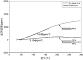
이와 같이 구성된 본 발명에 따른 인쇄회로기판을 앞서 언급된 제조 공정을 통해 제작하고, 종래의 일반적인 인쇄회로기판 즉, 코어 보강재를 사용하지 않고 절연재로만 형성된 절연층을 이용하여 제작된 인쇄회로기판과 본 발명에 따른 인쇄회로기판에 소정의 열을 가하고 그 열팽창률을 살펴보면 아래에 도시된 도 14와 같이 시뮬레이션된다.The printed circuit board according to the present invention constructed as described above is manufactured through the above-mentioned manufacturing process, and a conventional printed circuit board, that is, a printed circuit board manufactured by using an insulation layer formed only of an insulating material without using a core reinforcement material, and the present invention. Applying a predetermined heat to the printed circuit board according to the invention and looking at the coefficient of thermal expansion is simulated as shown in Figure 14 shown below.
도 14는 본 발명에 따른 제1 실시예의 인쇄회로기판과 종래 기술에 따른 인쇄회로기판의 휨 특성 시뮬레이션 그래프로서, 도시된 바와 같이 절연층 사이에 프리프레그 재질이 개재된 종래의 인쇄회로기판은 온도가 올라갈수록 휨을 유발하는 힘인 열팽창률이 급격히 커지게 되어 기판의 제조 공정 중에 휨 발생이 크게 발생되는 반면에, 본 발명에 따른 인쇄회로기판은 낮은 온도나 높은 온도에서 열팽창률의 변화가 크게 발생되지 않고 낮은 수준에서 유지되기 때문에 인쇄회로기판의 제작 공정 중에서 휨 발생이 최소화됨을 알 수 있다. 즉, 본 발명에 따른 인쇄회로기판은 코어를 구성하는 절연층 표면 또는 절연층 사이에 글라스 재질의 코어 보강재가 삽입됨에 따라 우수한 강성을 가지면서 인쇄회로기판의 제작 공정 중에 적용도는 온도와 습도 변화에 따른 휨이 최소화될 수 있도록 할 수 있다.
FIG. 14 is a graph illustrating a bending characteristic simulation of a printed circuit board according to a first embodiment of the present invention and a conventional printed circuit board. As illustrated, a conventional printed circuit board having a prepreg material interposed between insulating layers is used. While the thermal expansion coefficient, which is a force that causes warpage, increases rapidly, the warpage is greatly generated during the manufacturing process of the substrate, while the printed circuit board according to the present invention does not significantly change the thermal expansion rate at low or high temperatures. It can be seen that the warpage is minimized during the manufacturing process of the printed circuit board because it is maintained at a low level. That is, the printed circuit board according to the present invention has excellent rigidity as the glass core reinforcing material is inserted between the insulating layer surface or the insulating layer constituting the core, the degree of application during the manufacturing process of the printed circuit board changes in temperature and humidity It is possible to minimize the warpage due to.
한편, 앞서 언급된 실시예들의 기술적 특징을 갖는 본 발명의 인쇄회로기판은 종래의 인쇄회로기판에 비해 향상된 코어의 강성과 휨 특성을 구현하기 위하여 절연층과 코어 보강재로 이루어진 코어의 전체 두께 대비 코어 보강재가 차지하는 비율(portion)이 35% 내지 80%의 범위를 갖도록 하는 것이 바람직하다. 이는 앞서 설명한 제1 실시예의 인쇄회로기판(도 1)과 제2 실시예의 인쇄회로기판(도 6)에 채용되는 코어 구성에 모두 적용될 수 있다.On the other hand, the printed circuit board of the present invention having the technical features of the above-mentioned embodiments has a core compared to the total thickness of the core consisting of an insulating layer and a core reinforcement in order to implement the improved rigidity and bending characteristics of the core compared to the conventional printed circuit board It is desirable for the reinforcement to have a proportion in the range of 35% to 80%. This can be applied to both the core configuration employed in the printed circuit board (FIG. 1) of the first embodiment and the printed circuit board (FIG. 6) of the second embodiment described above.
또한, 각 실시예에서 코어를 구성하는 코어 보강재와 절연층의 열팽창계수(CTE)와 열팽창률의 관계에서 하기의 수학식 1을 만족할 때 종래의 인쇄회로기판에 비해 향상된 코어의 휨 특성을 구현할 수 있다.Further, in each embodiment, when the following

여기서, α1 : 코어 보강재의 열팽창계수(1/k),Where α 1 : coefficient of thermal expansion of the core reinforcing material (1 / k),
α2 : 절연층의 열팽창계수(1/k)이고,α 2 is the coefficient of thermal expansion of the insulating layer (1 / k),
E1 : 코어 보강재의 열팽창률(GPa)이고,E 1 is the coefficient of thermal expansion (GPa) of the core reinforcing material,
E2 : 절연재의 열팽창률(GPa)이다.
E 2 : Thermal expansion coefficient (GPa) of the insulating material.
여기서, 코어의 전체 두께 대비 코어 보강재가 차지하는 비율을 최하 35%로 한정하는 이유는 종래의 기판에서 코어 구조물보다 코어 보강재의 구성 비율이 35% 이상일 때 코어의 휨 특성이 향상될 수 있고, 최대 80% 이하로 한정하는 이유는 코어에서 코어 보강재를 제외한 절연층의 두께를 10㎛까지 제작할 수 있는 데, 절연층의 두께를 더 얇게 형성할 경우에는 코어에 크랙이 발생될 수 있고, 크랙 발생에 따른 코어의 파단이 발생될 수 있다.Here, the reason for limiting the ratio of the core reinforcement to the lowest 35% of the total thickness of the core is that the bending property of the core can be improved when the composition ratio of the core reinforcement is 35% or more than the core structure in the conventional substrate, up to 80 The reason for limiting to the% or less is that the thickness of the insulating layer except for the core reinforcement in the core can be manufactured up to 10 μm. When the thickness of the insulating layer is formed thinner, cracks may occur in the core, Breakage of the core may occur.
따라서, 상기 수학식을 통해 코어의 전체 두께에서 코어 보강재가 35% 내지 80%의 범위를 가지도록 하면서, 코어 보강재와 코어 보강재를 감싸는 절연층이 다양한 재질, 즉 PPG, ABF, PI 또는 프라이머(primer) 중 어느 하나로 구성된 절연층 또는 PPG, ABF, PI 또는 프라이머(primer) 중 어느 하나의 절연 재질에 글라스 크로스(glass cloth) 또는 필러 등이 함침된 절연층의 변수를 상기 수학식에 대입하여 6.492 × 10 ~ 4.463 × 10 / GPa·k의 범위를 만족한다면 코어의 휨 개선에 효과가 있다는 의미이다.
Therefore, the core reinforcement in the overall thickness of the core through the above equation to have a range of 35% to 80%, while the insulation layer surrounding the core reinforcement and the core reinforcement is a variety of materials, that is, PPG, ABF, PI or primer (primer) ) Into an insulating layer composed of any one of PPG, ABF, PI, or primer, and an insulating layer impregnated with a glass cloth or filler in the insulating material of 6.492 × If the range of 10 to 4.463 × 10 / GPa · k is satisfied, it means that the core is effective in improving warpage.
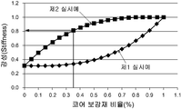
이와 같이 코어 전체의 두께에 대한 코어 보강재가 차지하는 비율과, 상기 수학식의 조건을 만족할 때, 도 15 또는 도 16에 도시된 바와 같이 코어의 강성과 휨 특성이 만족할 수 있다.As such, when the ratio of the core reinforcing material to the thickness of the entire core and the condition of the above equation are satisfied, as shown in FIG. 15 or FIG. 16, the rigidity and the bending property of the core may be satisfied.
도 15는 본 발명에 따른 제1 실시예와 제2 실시예의 인쇄회로기판에 대한 강성 특성 시뮬레이션 그래프이고, 도 16은 본 발명에 따른 제1 실시예와 제2 실시예의 인쇄회로기판에 대한 휨 특성 시뮬레이션 그래프이다.15 is a stiffness characteristic simulation graph of the printed circuit board of the first embodiment and the second embodiment according to the present invention, Figure 16 is a bending characteristic of the printed circuit board of the first embodiment and the second embodiment according to the present invention Simulation graph.
그래프에 도시된 바와 같이, 도 15와 도 16을 통해 살펴보면 앞서 설명한 인쇄회로기판의 제1 실시예와 제2 실시예는 종래의 인쇄회로기판의 코어(주로 CCL)에 비해 코어의 전체 두께 대비 코어 보강재가 차지하는 비율이 35% 이상에서 강성과 휨 특성이 모두 개선되고, 각 실시예 중에서 코어의 전체 두께 대비 코어 보강재가 차지하는 비율이 35% 이상일때 제1 실시예의 인쇄회로기판에 비해 제2 실시예의 인쇄회로기판이 약 2.5배 더 강한 강성을 가질 수 있고, 제1 실시예의 인쇄회로기판에 비해 제2 실시예의 인쇄회로기판이 미세하게 휨 특성이 더 우수한 개선 효과를 나타냄을 알 수 있다.
As shown in the graph, referring to FIGS. 15 and 16, the first and second embodiments of the above-described printed circuit board are compared to the total thickness of the core compared to the core of the conventional printed circuit board (mainly CCL). When the ratio of the reinforcing material occupies 35% or more, both the stiffness and the bending property are improved, and when the ratio of the core reinforcing material to the total thickness of the core is 35% or more in each embodiment, the ratio of the second embodiment to the printed circuit board of the first embodiment It can be seen that the printed circuit board may have about 2.5 times stronger rigidity, and the printed circuit board of the second embodiment exhibits a finer bending effect than the printed circuit board of the first embodiment.
상기에서는 본 발명의 바람직한 실시예를 참조하여 설명하였지만, 해당 기술 분야에서 통상의 지식을 가진 자라면 하기의 특허청구범위에 기재되는 본 발명의 사상 및 영역으로부터 벗어나지 않는 범위 내에서 본 발명을 다양하게 수정 및 변경시킬 수 있음을 이해할 수 있을 것이다.
While the present invention has been particularly shown and described with reference to exemplary embodiments thereof, it is to be understood that the invention is not limited to the disclosed exemplary embodiments. It will be understood that the invention may be varied and varied without departing from the scope of the invention.
100, 200, 300. 인쇄회로기판
110, 220. 코어 보강재
120, 210. 절연층
130, 270. 회로층
150, 250. 관통홀100, 200, 300. Printed Circuit Board
110, 220. Core reinforcement
120, 210. Insulation layer
130, 270. Circuit layer
150, 250.Through Hole
Claims (38)
를 포함하는 인쇄회로기판.
A core in which an insulating layer and a core reinforcement are laminated alternately;
And a printed circuit board.
상기 코어는, 상기 절연층 사이에 상기 코어 보강재가 개재된 인쇄회로기판.
The method of claim 1,
The core is a printed circuit board, the core reinforcing material is interposed between the insulating layer.
상기 코어는, 상기 절연층 양면에 상기 코어 보강재가 적층된 인쇄회로기판.
The method of claim 1,
The core is a printed circuit board in which the core reinforcing material is laminated on both sides of the insulating layer.
상기 코어 보강재는, 판 상의 글라스 재질로 구성된 인쇄회로기판.
The method of claim 1,
The core reinforcing material is a printed circuit board made of a plate-like glass material.
상기 코어 보강재는, 비전기전도성 고분자 재질의 필름 형태로 구성된 인쇄회로기판.
The method of claim 1,
The core reinforcing material is a printed circuit board composed of a film form of a non-conductive polymer material.
상기 코어 보강재는, 25 내지 200㎛의 두께로 형성된 인쇄회로기판.
The method according to claim 2 or 3,
The core reinforcing material is a printed circuit board formed to a thickness of 25 to 200㎛.
상기 절연층은, 복수의 절연층으로 구성된 인쇄회로기판.
The method of claim 3,
The insulating layer is a printed circuit board composed of a plurality of insulating layers.
상기 코어 보강재는, 상기 코어의 전체 두께에 대한 상기 코어 보강재 두께의 비율이 35% 내지 80%의 범위를 갖는 인쇄회로기판.
The method of claim 1,
The core reinforcing member, the ratio of the thickness of the core reinforcing material to the total thickness of the core has a range of 35% to 80%.
상기 코어는, 상기 코어 보강재와 절연층의 열팽창계수(CTE)와 열팽창률의 관계에서 휨 특성에 대하여 하기의 수학식을 만족하는 인쇄회로기판.
수학식

여기서, α1 : 코어 보강재의 열팽창계수(1/k),
α2 : 절연층의 열팽창계수(1/k),
E1 : 코어 보강재의 열팽창률(GPa),
E2 : 절연재의 열팽창률(GPa).
The method of claim 1,
And the core satisfies the following equation for the bending property in the relationship between the coefficient of thermal expansion (CTE) and the coefficient of thermal expansion of the core reinforcing material, the insulating layer.
Equation
Where α 1 : coefficient of thermal expansion of the core reinforcing material (1 / k),
α 2 : coefficient of thermal expansion of the insulating layer (1 / k),
E 1 : coefficient of thermal expansion (GPa) of the core reinforcement,
E 2 : Thermal expansion coefficient (GPa) of an insulating material.
상기 코어 보강재의 양면에 형성된 절연층;
상기 절연층과 코어 보강재를 관통하여 형성된 관통홀; 및
상기 절연층 상에 형성된 회로층과 상기 회로층의 층간 연결을 위하여 상기 관통홀에 형성된 도금층;
을 포함하는 인쇄회로기판.
Core reinforcement provided with rigidity;
Insulating layers formed on both surfaces of the core reinforcing material;
A through hole formed through the insulating layer and the core reinforcement material; And
A plating layer formed in the through hole for connecting the circuit layer formed on the insulating layer and the layer between the circuit layer;
And a printed circuit board.
상기 코어 보강재와 절연층 사이의 상기 코어 보강재 표면에는 코팅층이 더 형성된 인쇄회로기판.
11. The method of claim 10,
The printed circuit board further comprising a coating layer on the surface of the core reinforcing material between the core reinforcing material and the insulating layer.
상기 코팅층은, 2㎛ 이하의 두께로 형성된 인쇄회로기판.
12. The method of claim 11,
The coating layer is a printed circuit board formed to a thickness of 2㎛ or less.
상기 코어 보강재는, 판 상의 글라스 또는 비전기전도성 고분자 재질의 필름 형태로 구성된 인쇄회로기판.
11. The method of claim 10,
The core reinforcing material is a printed circuit board consisting of a film on the plate glass or non-conductive polymer material.
상기 절연층은, 글라스 패브릭이 함침된 절연재로 구성되는 인쇄회로기판.
11. The method of claim 10,
The insulating layer is a printed circuit board composed of an insulating material impregnated with a glass fabric.
상기 코어 보강재는, 25 내지 200㎛의 두께로 형성된 인쇄회로기판.
11. The method of claim 10,
The core reinforcing material is a printed circuit board formed to a thickness of 25 to 200㎛.
상기 코어 보강재와 절연층을 포함하는 두께에 대하여 상기 코어 보강재 두께의 비율이 35% 내지 80%의 범위를 갖는 인쇄회로기판.
11. The method of claim 10,
And a ratio of the thickness of the core reinforcement to the thickness of the core reinforcement and the insulation layer is in a range of 35% to 80%.
상기 코어 보강재의 양면에 절연층을 형성하는 단계;
상기 코어 보강재와 절연층을 관통하는 관통홀을 형성하는 단계; 및
상기 관통홀의 내부에 도금층을 형성함과 아울러 상기 절연층의 표면에 회로층을 형성하는 단계; 를 포함하는 인쇄회로기판의 제조방법.
Preparing a core reinforcement;
Forming insulating layers on both sides of the core reinforcing material;
Forming a through hole penetrating the core reinforcing material and the insulating layer; And
Forming a plating layer on the inside of the through hole and forming a circuit layer on the surface of the insulating layer; And a step of forming the printed circuit board.
상기 코어 보강재는, 강성이 구비된 판 상의 글라스 또는 비전기전도성 고분자 재질의 필름 형태로 구성된 인쇄회로기판의 제조방법.
18. The method of claim 17,
The core reinforcing material is a manufacturing method of a printed circuit board consisting of a film of glass or non-conductive polymer material on the plate provided with rigidity.
상기 절연층을 형성하는 단계 이전에,
상기 코어 보강재의 일면 또는 양면에 코팅층이 형성되는 단계;를 더 포함하는 인쇄회로기판의 제조방법.
18. The method of claim 17,
Prior to forming the insulating layer,
And forming a coating layer on one or both surfaces of the core reinforcing material.
상기 코팅층은, 2㎛ 이하의 두께로 형성된 인쇄회로기판의 제조방법.
20. The method of claim 19,
The coating layer is a manufacturing method of a printed circuit board having a thickness of 2㎛ or less.
상기 관통홀을 형성하는 단계 이전에,
상기 절연층 상에 금속 박막이 형성되는 단계;를 더 포함하는 인쇄회로기판의 제조방법.
18. The method of claim 17,
Before forming the through hole,
Forming a metal thin film on the insulating layer; manufacturing method of a printed circuit board further comprising.
상기 금속 박막은, 상기 코어 보강재 표면에 상기 절연층이 형성됨과 동시에 형성되는 인쇄회로기판의 제조방법.
22. The method of claim 21,
The metal thin film is a method of manufacturing a printed circuit board is formed at the same time as the insulating layer is formed on the surface of the core reinforcing material.
상기 도금층은, 전기 동도금에 의해 형성되며, 상기 절연층 상면에 형성된 상기 회로층 형성을 위한 도금층과 동시에 형성되는 인쇄회로기판의 제조방법.
18. The method of claim 17,
The plating layer is formed by electroplating, and is formed simultaneously with the plating layer for forming the circuit layer formed on the insulating layer upper surface printed circuit board manufacturing method.
상기 절연층의 양면에 적층된 코어 보강재;
상기 절연층과 코어 보강재를 관통하여 형성된 관통홀; 및
상기 코어 보강재 상에 형성된 회로층;을 포함하는 인쇄회로기판.
Insulating layer;
A core reinforcing material laminated on both sides of the insulating layer;
A through hole formed through the insulating layer and the core reinforcement material; And
Printed circuit board comprising a; circuit layer formed on the core reinforcing material.
상기 절연층은, 복수의 절연층으로 형성된 인쇄회로기판.
25. The method of claim 24,
The insulating layer is a printed circuit board formed of a plurality of insulating layers.
상기 절연층과 코어 보강재를 포함하는 두께에 대하여 상기 코어 보강재 두께의 비율이 35% 내지 80%의 범위를 갖는 인쇄회로기판.
25. The method of claim 24,
And a ratio of the thickness of the core reinforcement to the thickness of the insulation layer and the core reinforcement in a range of 35% to 80%.
상기 코어 보강재는, 판 상의 글라스 또는 비전기전도성 고분자 재질의 필름 형태로 구성된 인쇄회로기판.
25. The method of claim 24,
The core reinforcing material is a printed circuit board consisting of a film on the plate glass or non-conductive polymer material.
상기 절연층은, 글라스 패브릭이 함침된 절연재로 구성되는 인쇄회로기판.
25. The method of claim 24,
The insulating layer is a printed circuit board composed of an insulating material impregnated with a glass fabric.
상기 회로층은, 상기 코어 보강재 상에 형성된 시드층; 및
상기 시드층 상에 형성된 도금층; 을 더 포함하는 인쇄회로기판.
25. The method of claim 24,
The circuit layer, the seed layer formed on the core reinforcing material; And
A plating layer formed on the seed layer; And a printed circuit board.
상기 시드층은, 티타늄(Ti), 구리(Cu), 몰리브덴(Mo), 니켈(Ni), 은(Ag), 아연(Zn), 탄소(C) 등의 전도성 금속재 또는 이들의 합금으로 이루어진 군으로부터 선택된 어느 하나인 인쇄회로기판.
30. The method of claim 29,
The seed layer is made of a conductive metal material such as titanium (Ti), copper (Cu), molybdenum (Mo), nickel (Ni), silver (Ag), zinc (Zn), carbon (C), or an alloy thereof. The printed circuit board is any one selected from.
상기 코어 보강재 상에 시드층을 형성하는 단계;
상기 시드층 상에 회로 형성용 개구부를 갖는 도금 레지스트층을 형성하는 단계;
상기 회로 형성용 개구부에 도금층을 형성하는 단계; 및
상기 도금 레지스트층을 제거하여 회로층을 형성하는 단계;를 포함하는 인쇄회로기판의 제조방법.
Bonding the core reinforcement to both sides of the insulating layer;
Forming a seed layer on the core stiffener;
Forming a plating resist layer having an opening for forming a circuit on the seed layer;
Forming a plating layer in the opening for forming the circuit; And
Removing the plating resist layer to form a circuit layer.
상기 절연층에 코어 보강재를 접합하는 단계에서,
상기 절연층의 양면에 코어 보강재를 배치시키는 단계; 및
상기 코어 보강재 상에서 가열 공정과 가압 공정을 통해 상기 절연층과 코어 보강재를 접합하는 단계;를 더 포함하는 인쇄회로기판의 제조방법.
32. The method of claim 31,
Bonding the core reinforcement to the insulating layer,
Disposing a core reinforcement on both sides of the insulating layer; And
Bonding the insulation layer and the core reinforcement on the core reinforcement through a heating process and a pressing process.
상기 시드층을 형성하는 단계 이전에,
상기 절연층과 코어 보강재를 관통하는 관통홀을 가공하는 단계;를 더 포함하는 인쇄회로기판의 제조방법.
32. The method of claim 31,
Prior to forming the seed layer,
And processing a through hole penetrating through the insulating layer and the core reinforcement.
상기 관통홀을 가공하는 단계 이후에,
상기 코어 보강재의 표면과 상기 관통홀의 내벽을 클리닝하는 단계;를 더 포함하는 인쇄회로기판의 제조방법.
34. The method of claim 33,
After the step of processing the through hole,
And cleaning the surface of the core reinforcing material and the inner wall of the through hole.
상기 코어 보강재는, 강성이 구비된 판 상의 글라스 또는 비전기전도성 고분자 재질의 필름 형태로 구성된 인쇄회로기판의 제조방법.
32. The method of claim 31,
The core reinforcing material is a manufacturing method of a printed circuit board consisting of a film of glass or non-conductive polymer material on the plate provided with rigidity.
상기 클리닝하는 단계는,
건식 에칭 또는 습식 에칭을 통해 수행되는 인쇄회로기판의 제조방법.
35. The method of claim 34,
The cleaning step,
A method of manufacturing a printed circuit board carried out by dry etching or wet etching.
상기 코어 보강재와 절연층의 열팽창계수(CTE)와 열팽창률의 관계에서 휨 특성에 대하여 하기의 수학식을 만족하는 인쇄회로기판.
수학식

여기서, α1 : 코어 보강재의 열팽창계수(1/k),
α2 : 절연층의 열팽창계수(1/k),
E1 : 코어 보강재의 열팽창률(GPa),
E2 : 절연재의 열팽창률(GPa).
The method of claim 10 or 24,
The printed circuit board satisfies the following equation for the bending property in the relationship between the coefficient of thermal expansion (CTE) and the coefficient of thermal expansion of the core reinforcing material, the insulating layer.
Equation
Where α 1 : coefficient of thermal expansion of the core reinforcing material (1 / k),
α 2 : coefficient of thermal expansion of the insulating layer (1 / k),
E 1 : coefficient of thermal expansion (GPa) of the core reinforcement,
E 2 : Thermal expansion coefficient (GPa) of an insulating material.
상기 절연층과 코어 보강재가 교호로 적층된 코어의 상, 하면에 제2 절연층을 적층하고, 상기 제2 절연층 상에 회로층이 형성되어 빌드업되고, 상기 제2 절연층에 형성된 비아홀을 통해 상기 회로층의 도통이 이루어지며, 상기 제2 절연층 상에 솔더 레지스트층이 형성된 인쇄회로기판.The method according to claim 1 or 10 or 24,
A second insulating layer is laminated on the upper and lower surfaces of the core in which the insulating layer and the core reinforcing material are alternately stacked, and a circuit layer is formed on the second insulating layer to build up the via hole formed in the second insulating layer. The conductive circuit of the circuit layer is made through, the printed circuit board formed with a solder resist layer on the second insulating layer.
Priority Applications (4)
| Application Number | Priority Date | Filing Date | Title |
|---|---|---|---|
| TW102126939A TWI595811B (en) | 2012-07-30 | 2013-07-26 | Printed circuit board and method for manufacturing the same |
| US13/951,886 US20140027163A1 (en) | 2012-07-30 | 2013-07-26 | Printed circuit board and method for manufacturing the same |
| JP2013157429A JP2014027284A (en) | 2012-07-30 | 2013-07-30 | Printed circuit board and manufacturing method of the same |
| JP2015080094A JP6342357B2 (en) | 2012-07-30 | 2015-04-09 | Printed circuit board and manufacturing method thereof |
Applications Claiming Priority (4)
| Application Number | Priority Date | Filing Date | Title |
|---|---|---|---|
| KR1020120083160 | 2012-07-30 | ||
| KR20120083160 | 2012-07-30 | ||
| KR20120140480 | 2012-12-05 | ||
| KR1020120140480 | 2012-12-05 |
Related Child Applications (1)
| Application Number | Title | Priority Date | Filing Date |
|---|---|---|---|
| KR1020150040298A Division KR101903557B1 (en) | 2015-03-23 | 2015-03-23 | A printed circuit board and a method for manufacturing |
Publications (1)
| Publication Number | Publication Date |
|---|---|
| KR20140016150A true KR20140016150A (en) | 2014-02-07 |
Family
ID=50265370
Family Applications (1)
| Application Number | Title | Priority Date | Filing Date |
|---|---|---|---|
| KR1020130061168A KR20140016150A (en) | 2012-07-30 | 2013-05-29 | A printed circuit board and a method for manufacturing |
Country Status (3)
| Country | Link |
|---|---|
| JP (1) | JP6342357B2 (en) |
| KR (1) | KR20140016150A (en) |
| TW (1) | TWI595811B (en) |
Cited By (3)
| Publication number | Priority date | Publication date | Assignee | Title |
|---|---|---|---|---|
| KR20160020761A (en) * | 2014-08-14 | 2016-02-24 | 삼성전기주식회사 | Printed circuit board and method of manufacturing the same |
| KR20160036247A (en) * | 2014-09-25 | 2016-04-04 | 코닝정밀소재 주식회사 | Substrate for ic package |
| KR20170001310A (en) | 2015-06-26 | 2017-01-04 | 삼성전기주식회사 | Glass core substrate, manufacturing method thereof and circuit board |
Families Citing this family (1)
| Publication number | Priority date | Publication date | Assignee | Title |
|---|---|---|---|---|
| TWI685288B (en) * | 2018-08-22 | 2020-02-11 | 健鼎科技股份有限公司 | Circuit board and manufacturing method thereof |
Family Cites Families (8)
| Publication number | Priority date | Publication date | Assignee | Title |
|---|---|---|---|---|
| JPS4946165A (en) * | 1972-09-11 | 1974-05-02 | ||
| JP3756041B2 (en) * | 1999-05-27 | 2006-03-15 | Hoya株式会社 | Manufacturing method of multilayer printed wiring board |
| JP4134172B2 (en) * | 2003-09-09 | 2008-08-13 | Hoya株式会社 | Manufacturing method of double-sided wiring glass substrate |
| JP2005159330A (en) * | 2003-11-05 | 2005-06-16 | Hitachi Chem Co Ltd | Method of manufacturing multilayer circuit board and multilayer circuit board manufactured by the same, and board with semiconductor chip mounted thereon and semiconductor package using the same |
| TWI236324B (en) * | 2004-04-08 | 2005-07-11 | Phoenix Prec Technology Corp | Insulating structure of circuit board and method for fabricating the circuit board by using the insulating structure |
| JP2006049804A (en) * | 2004-07-07 | 2006-02-16 | Shinko Electric Ind Co Ltd | Manufacturing method of wiring board |
| JP4564342B2 (en) * | 2004-11-24 | 2010-10-20 | 大日本印刷株式会社 | Multilayer wiring board and manufacturing method thereof |
| WO2011027558A1 (en) * | 2009-09-02 | 2011-03-10 | パナソニック株式会社 | Printed wiring board, build-up multi-layer board, and production method therefor |
-
2013
- 2013-05-29 KR KR1020130061168A patent/KR20140016150A/en not_active Application Discontinuation
- 2013-07-26 TW TW102126939A patent/TWI595811B/en active
-
2015
- 2015-04-09 JP JP2015080094A patent/JP6342357B2/en active Active
Cited By (3)
| Publication number | Priority date | Publication date | Assignee | Title |
|---|---|---|---|---|
| KR20160020761A (en) * | 2014-08-14 | 2016-02-24 | 삼성전기주식회사 | Printed circuit board and method of manufacturing the same |
| KR20160036247A (en) * | 2014-09-25 | 2016-04-04 | 코닝정밀소재 주식회사 | Substrate for ic package |
| KR20170001310A (en) | 2015-06-26 | 2017-01-04 | 삼성전기주식회사 | Glass core substrate, manufacturing method thereof and circuit board |
Also Published As
| Publication number | Publication date |
|---|---|
| JP2015128195A (en) | 2015-07-09 |
| JP6342357B2 (en) | 2018-06-13 |
| TWI595811B (en) | 2017-08-11 |
| TW201414367A (en) | 2014-04-01 |
Similar Documents
| Publication | Publication Date | Title |
|---|---|---|
| JP2014027284A (en) | Printed circuit board and manufacturing method of the same | |
| US7002080B2 (en) | Multilayer wiring board | |
| JP4199198B2 (en) | Multilayer wiring board and manufacturing method thereof | |
| KR101044127B1 (en) | Heat-dissipating substrate and fabricating method of the same | |
| JP5681824B1 (en) | Wiring board assembly and manufacturing method thereof | |
| JP4689375B2 (en) | Laminated substrate and electronic device having the laminated substrate | |
| US9711440B2 (en) | Wiring board and method for manufacturing the same | |
| US20070069360A1 (en) | Semiconductor package substrate having different thicknesses between wire bonding pad and ball pad and method for fabricating the same | |
| JP2006190928A (en) | Bga package and its manufacturing method | |
| KR101181105B1 (en) | The radiant heat circuit board and the method for manufacturing the same | |
| JP6342357B2 (en) | Printed circuit board and manufacturing method thereof | |
| JP2006269979A (en) | Flexible rigid printed-wiring board and its manufacturing method | |
| KR101903557B1 (en) | A printed circuit board and a method for manufacturing | |
| JP6444651B2 (en) | Multilayer printed wiring board | |
| JP5141084B2 (en) | Electronic component mounting wiring board and method for preventing peeling of electronic component in electronic component mounting wiring board | |
| KR20190042840A (en) | Metal core printed circuit board and method of manufacturing the same | |
| KR101177651B1 (en) | Printed circuit board and method of manufacturing the same | |
| WO2021084860A1 (en) | Wiring board | |
| KR101518067B1 (en) | Multilayer printed wiring board and its manufacturing method | |
| JP4070193B2 (en) | Wiring board and electronic component mounting structure | |
| KR20140123273A (en) | Printed circuit board and manufacturing method thereof | |
| JP2015038908A (en) | Flex-rigid wiring board | |
| KR102281457B1 (en) | Printed circuit board and method of manufacturing the same | |
| KR20170067459A (en) | Package substrate | |
| KR100888562B1 (en) | Method of fabricating an active device embedded printer circuit board |
Legal Events
| Date | Code | Title | Description |
|---|---|---|---|
| A201 | Request for examination | ||
| E902 | Notification of reason for refusal | ||
| AMND | Amendment | ||
| E601 | Decision to refuse application | ||
| A107 | Divisional application of patent | ||
| AMND | Amendment | ||
| E902 | Notification of reason for refusal |