KR20130128439A - Articles having optical adhesives and method of making same - Google Patents
Articles having optical adhesives and method of making same Download PDFInfo
- Publication number
- KR20130128439A KR20130128439A KR1020137018861A KR20137018861A KR20130128439A KR 20130128439 A KR20130128439 A KR 20130128439A KR 1020137018861 A KR1020137018861 A KR 1020137018861A KR 20137018861 A KR20137018861 A KR 20137018861A KR 20130128439 A KR20130128439 A KR 20130128439A
- Authority
- KR
- South Korea
- Prior art keywords
- optical
- substrate
- film
- loca
- optical film
- Prior art date
Links
- 230000003287 optical effect Effects 0.000 title claims abstract description 132
- 230000001070 adhesive effect Effects 0.000 title claims abstract description 75
- 239000000853 adhesive Substances 0.000 title claims abstract description 74
- 238000004519 manufacturing process Methods 0.000 title claims description 5
- 239000012788 optical film Substances 0.000 claims abstract description 60
- 239000010408 film Substances 0.000 claims abstract description 56
- 238000010168 coupling process Methods 0.000 claims abstract description 54
- 230000008878 coupling Effects 0.000 claims abstract description 53
- 238000005859 coupling reaction Methods 0.000 claims abstract description 53
- 239000007788 liquid Substances 0.000 claims abstract description 20
- 230000005540 biological transmission Effects 0.000 claims abstract description 17
- 239000000758 substrate Substances 0.000 claims description 163
- 238000000034 method Methods 0.000 claims description 20
- 230000005855 radiation Effects 0.000 claims description 10
- 238000010521 absorption reaction Methods 0.000 claims description 6
- 238000012937 correction Methods 0.000 claims description 4
- 238000010030 laminating Methods 0.000 claims description 4
- 238000012876 topography Methods 0.000 claims description 2
- 238000009792 diffusion process Methods 0.000 claims 1
- 230000003014 reinforcing effect Effects 0.000 abstract 1
- 239000010410 layer Substances 0.000 description 81
- 239000011521 glass Substances 0.000 description 34
- NIXOWILDQLNWCW-UHFFFAOYSA-M Acrylate Chemical compound [O-]C(=O)C=C NIXOWILDQLNWCW-UHFFFAOYSA-M 0.000 description 18
- 239000000203 mixture Substances 0.000 description 17
- 239000004820 Pressure-sensitive adhesive Substances 0.000 description 14
- 238000003475 lamination Methods 0.000 description 10
- 239000004973 liquid crystal related substance Substances 0.000 description 10
- 230000000712 assembly Effects 0.000 description 8
- 238000000429 assembly Methods 0.000 description 8
- 230000008569 process Effects 0.000 description 8
- -1 2-ethylhexyl Chemical group 0.000 description 7
- 238000012360 testing method Methods 0.000 description 7
- NIXOWILDQLNWCW-UHFFFAOYSA-N 2-Propenoic acid Natural products OC(=O)C=C NIXOWILDQLNWCW-UHFFFAOYSA-N 0.000 description 6
- 239000000463 material Substances 0.000 description 6
- 239000000178 monomer Substances 0.000 description 6
- 229920000642 polymer Polymers 0.000 description 6
- DXPPIEDUBFUSEZ-UHFFFAOYSA-N 6-methylheptyl prop-2-enoate Chemical compound CC(C)CCCCCOC(=O)C=C DXPPIEDUBFUSEZ-UHFFFAOYSA-N 0.000 description 5
- 150000001252 acrylic acid derivatives Chemical class 0.000 description 5
- 230000032683 aging Effects 0.000 description 5
- 238000000576 coating method Methods 0.000 description 5
- 238000010586 diagram Methods 0.000 description 5
- 125000002768 hydroxyalkyl group Chemical group 0.000 description 5
- 238000002360 preparation method Methods 0.000 description 5
- GOXQRTZXKQZDDN-UHFFFAOYSA-N 2-Ethylhexyl acrylate Chemical compound CCCCC(CC)COC(=O)C=C GOXQRTZXKQZDDN-UHFFFAOYSA-N 0.000 description 4
- BAPJBEWLBFYGME-UHFFFAOYSA-N Methyl acrylate Chemical compound COC(=O)C=C BAPJBEWLBFYGME-UHFFFAOYSA-N 0.000 description 4
- 125000000217 alkyl group Chemical group 0.000 description 4
- CQEYYJKEWSMYFG-UHFFFAOYSA-N butyl acrylate Chemical compound CCCCOC(=O)C=C CQEYYJKEWSMYFG-UHFFFAOYSA-N 0.000 description 4
- 229920001971 elastomer Polymers 0.000 description 4
- 239000000806 elastomer Substances 0.000 description 4
- 229920000193 polymethacrylate Polymers 0.000 description 4
- 239000011347 resin Substances 0.000 description 4
- 229920005989 resin Polymers 0.000 description 4
- 230000035882 stress Effects 0.000 description 4
- 238000002834 transmittance Methods 0.000 description 4
- HRPVXLWXLXDGHG-UHFFFAOYSA-N Acrylamide Chemical compound NC(=O)C=C HRPVXLWXLXDGHG-UHFFFAOYSA-N 0.000 description 3
- YXFVVABEGXRONW-UHFFFAOYSA-N Toluene Chemical compound CC1=CC=CC=C1 YXFVVABEGXRONW-UHFFFAOYSA-N 0.000 description 3
- 230000015572 biosynthetic process Effects 0.000 description 3
- 238000010438 heat treatment Methods 0.000 description 3
- 229920002635 polyurethane Polymers 0.000 description 3
- 239000004814 polyurethane Substances 0.000 description 3
- 239000007787 solid Substances 0.000 description 3
- VZCYOOQTPOCHFL-UHFFFAOYSA-N trans-butenedioic acid Natural products OC(=O)C=CC(O)=O VZCYOOQTPOCHFL-UHFFFAOYSA-N 0.000 description 3
- 125000000391 vinyl group Chemical group [H]C([*])=C([H])[H] 0.000 description 3
- 229920002554 vinyl polymer Polymers 0.000 description 3
- PSGCQDPCAWOCSH-UHFFFAOYSA-N (4,7,7-trimethyl-3-bicyclo[2.2.1]heptanyl) prop-2-enoate Chemical compound C1CC2(C)C(OC(=O)C=C)CC1C2(C)C PSGCQDPCAWOCSH-UHFFFAOYSA-N 0.000 description 2
- 229920003314 Elvaloy® Polymers 0.000 description 2
- VGGSQFUCUMXWEO-UHFFFAOYSA-N Ethene Chemical compound C=C VGGSQFUCUMXWEO-UHFFFAOYSA-N 0.000 description 2
- 239000005977 Ethylene Substances 0.000 description 2
- VZCYOOQTPOCHFL-OWOJBTEDSA-N Fumaric acid Chemical compound OC(=O)\C=C\C(O)=O VZCYOOQTPOCHFL-OWOJBTEDSA-N 0.000 description 2
- KFZMGEQAYNKOFK-UHFFFAOYSA-N Isopropanol Chemical compound CC(C)O KFZMGEQAYNKOFK-UHFFFAOYSA-N 0.000 description 2
- 239000000654 additive Substances 0.000 description 2
- 230000000903 blocking effect Effects 0.000 description 2
- 230000003749 cleanliness Effects 0.000 description 2
- 239000011248 coating agent Substances 0.000 description 2
- 230000007547 defect Effects 0.000 description 2
- 230000032798 delamination Effects 0.000 description 2
- UHESRSKEBRADOO-UHFFFAOYSA-N ethyl carbamate;prop-2-enoic acid Chemical compound OC(=O)C=C.CCOC(N)=O UHESRSKEBRADOO-UHFFFAOYSA-N 0.000 description 2
- 239000007789 gas Substances 0.000 description 2
- 150000002734 metacrylic acid derivatives Chemical class 0.000 description 2
- 238000002156 mixing Methods 0.000 description 2
- 239000004014 plasticizer Substances 0.000 description 2
- 230000010287 polarization Effects 0.000 description 2
- 229920003229 poly(methyl methacrylate) Polymers 0.000 description 2
- 229920006267 polyester film Polymers 0.000 description 2
- 229920000307 polymer substrate Polymers 0.000 description 2
- 239000004926 polymethyl methacrylate Substances 0.000 description 2
- 229920001296 polysiloxane Polymers 0.000 description 2
- 230000035939 shock Effects 0.000 description 2
- 239000002356 single layer Substances 0.000 description 2
- 238000003860 storage Methods 0.000 description 2
- 238000010998 test method Methods 0.000 description 2
- 238000003878 thermal aging Methods 0.000 description 2
- 238000009736 wetting Methods 0.000 description 2
- JWYVGKFDLWWQJX-UHFFFAOYSA-N 1-ethenylazepan-2-one Chemical compound C=CN1CCCCCC1=O JWYVGKFDLWWQJX-UHFFFAOYSA-N 0.000 description 1
- KWKAKUADMBZCLK-UHFFFAOYSA-N 1-octene Chemical compound CCCCCCC=C KWKAKUADMBZCLK-UHFFFAOYSA-N 0.000 description 1
- 125000004493 2-methylbut-1-yl group Chemical group CC(C*)CC 0.000 description 1
- NCTBYWFEJFTVEL-UHFFFAOYSA-N 2-methylbutyl prop-2-enoate Chemical compound CCC(C)COC(=O)C=C NCTBYWFEJFTVEL-UHFFFAOYSA-N 0.000 description 1
- CFVWNXQPGQOHRJ-UHFFFAOYSA-N 2-methylpropyl prop-2-enoate Chemical compound CC(C)COC(=O)C=C CFVWNXQPGQOHRJ-UHFFFAOYSA-N 0.000 description 1
- ZVYGIPWYVVJFRW-UHFFFAOYSA-N 3-methylbutyl prop-2-enoate Chemical compound CC(C)CCOC(=O)C=C ZVYGIPWYVVJFRW-UHFFFAOYSA-N 0.000 description 1
- BVDBXCXQMHBGQM-UHFFFAOYSA-N 4-methylpentan-2-yl prop-2-enoate Chemical compound CC(C)CC(C)OC(=O)C=C BVDBXCXQMHBGQM-UHFFFAOYSA-N 0.000 description 1
- CUXGDKOCSSIRKK-UHFFFAOYSA-N 7-methyloctyl prop-2-enoate Chemical compound CC(C)CCCCCCOC(=O)C=C CUXGDKOCSSIRKK-UHFFFAOYSA-N 0.000 description 1
- COCLLEMEIJQBAG-UHFFFAOYSA-N 8-methylnonyl 2-methylprop-2-enoate Chemical compound CC(C)CCCCCCCOC(=O)C(C)=C COCLLEMEIJQBAG-UHFFFAOYSA-N 0.000 description 1
- LVGFPWDANALGOY-UHFFFAOYSA-N 8-methylnonyl prop-2-enoate Chemical compound CC(C)CCCCCCCOC(=O)C=C LVGFPWDANALGOY-UHFFFAOYSA-N 0.000 description 1
- GAWIXWVDTYZWAW-UHFFFAOYSA-N C[CH]O Chemical group C[CH]O GAWIXWVDTYZWAW-UHFFFAOYSA-N 0.000 description 1
- 229920000089 Cyclic olefin copolymer Polymers 0.000 description 1
- CERQOIWHTDAKMF-UHFFFAOYSA-N Methacrylic acid Chemical compound CC(=C)C(O)=O CERQOIWHTDAKMF-UHFFFAOYSA-N 0.000 description 1
- WHNWPMSKXPGLAX-UHFFFAOYSA-N N-Vinyl-2-pyrrolidone Chemical compound C=CN1CCCC1=O WHNWPMSKXPGLAX-UHFFFAOYSA-N 0.000 description 1
- MKYBYDHXWVHEJW-UHFFFAOYSA-N N-[1-oxo-1-(2,4,6,7-tetrahydrotriazolo[4,5-c]pyridin-5-yl)propan-2-yl]-2-[[3-(trifluoromethoxy)phenyl]methylamino]pyrimidine-5-carboxamide Chemical compound O=C(C(C)NC(=O)C=1C=NC(=NC=1)NCC1=CC(=CC=C1)OC(F)(F)F)N1CC2=C(CC1)NN=N2 MKYBYDHXWVHEJW-UHFFFAOYSA-N 0.000 description 1
- OAICVXFJPJFONN-UHFFFAOYSA-N Phosphorus Chemical compound [P] OAICVXFJPJFONN-UHFFFAOYSA-N 0.000 description 1
- 239000004793 Polystyrene Substances 0.000 description 1
- 229920002396 Polyurea Polymers 0.000 description 1
- OFOBLEOULBTSOW-UHFFFAOYSA-N Propanedioic acid Natural products OC(=O)CC(O)=O OFOBLEOULBTSOW-UHFFFAOYSA-N 0.000 description 1
- 239000012963 UV stabilizer Substances 0.000 description 1
- 239000002313 adhesive film Substances 0.000 description 1
- 239000002390 adhesive tape Substances 0.000 description 1
- 125000005250 alkyl acrylate group Chemical group 0.000 description 1
- 125000005233 alkylalcohol group Chemical group 0.000 description 1
- 239000003963 antioxidant agent Substances 0.000 description 1
- 230000008901 benefit Effects 0.000 description 1
- 229920001400 block copolymer Polymers 0.000 description 1
- 125000000484 butyl group Chemical group [H]C([*])([H])C([H])([H])C([H])([H])C([H])([H])[H] 0.000 description 1
- 125000004432 carbon atom Chemical group C* 0.000 description 1
- 230000008859 change Effects 0.000 description 1
- 239000003795 chemical substances by application Substances 0.000 description 1
- 238000003776 cleavage reaction Methods 0.000 description 1
- 239000002131 composite material Substances 0.000 description 1
- 238000009833 condensation Methods 0.000 description 1
- 230000005494 condensation Effects 0.000 description 1
- 239000004020 conductor Substances 0.000 description 1
- 229920001577 copolymer Polymers 0.000 description 1
- 238000004132 cross linking Methods 0.000 description 1
- FWLDHHJLVGRRHD-UHFFFAOYSA-N decyl prop-2-enoate Chemical compound CCCCCCCCCCOC(=O)C=C FWLDHHJLVGRRHD-UHFFFAOYSA-N 0.000 description 1
- 238000013461 design Methods 0.000 description 1
- 230000004069 differentiation Effects 0.000 description 1
- 239000000975 dye Substances 0.000 description 1
- 238000010894 electron beam technology Methods 0.000 description 1
- 125000001495 ethyl group Chemical group [H]C([H])([H])C([H])([H])* 0.000 description 1
- 238000013265 extended release Methods 0.000 description 1
- 239000000835 fiber Substances 0.000 description 1
- 239000005357 flat glass Substances 0.000 description 1
- 239000001530 fumaric acid Substances 0.000 description 1
- 239000003292 glue Substances 0.000 description 1
- 230000020169 heat generation Effects 0.000 description 1
- LNMQRPPRQDGUDR-UHFFFAOYSA-N hexyl prop-2-enoate Chemical compound CCCCCCOC(=O)C=C LNMQRPPRQDGUDR-UHFFFAOYSA-N 0.000 description 1
- APFVFJFRJDLVQX-UHFFFAOYSA-N indium atom Chemical compound [In] APFVFJFRJDLVQX-UHFFFAOYSA-N 0.000 description 1
- 229910003437 indium oxide Inorganic materials 0.000 description 1
- 125000001449 isopropyl group Chemical group [H]C([H])([H])C([H])(*)C([H])([H])[H] 0.000 description 1
- PBOSTUDLECTMNL-UHFFFAOYSA-N lauryl acrylate Chemical compound CCCCCCCCCCCCOC(=O)C=C PBOSTUDLECTMNL-UHFFFAOYSA-N 0.000 description 1
- 230000014759 maintenance of location Effects 0.000 description 1
- 229940049920 malate Drugs 0.000 description 1
- VZCYOOQTPOCHFL-UPHRSURJSA-N maleic acid Chemical compound OC(=O)\C=C/C(O)=O VZCYOOQTPOCHFL-UPHRSURJSA-N 0.000 description 1
- 239000011976 maleic acid Substances 0.000 description 1
- 239000008204 material by function Substances 0.000 description 1
- 239000011159 matrix material Substances 0.000 description 1
- 238000005259 measurement Methods 0.000 description 1
- 125000002496 methyl group Chemical group [H]C([H])([H])* 0.000 description 1
- 238000012986 modification Methods 0.000 description 1
- 230000004048 modification Effects 0.000 description 1
- 125000004108 n-butyl group Chemical group [H]C([H])([H])C([H])([H])C([H])([H])C([H])([H])* 0.000 description 1
- 125000004123 n-propyl group Chemical group [H]C([H])([H])C([H])([H])C([H])([H])* 0.000 description 1
- 229910052754 neon Inorganic materials 0.000 description 1
- GKAOGPIIYCISHV-UHFFFAOYSA-N neon atom Chemical compound [Ne] GKAOGPIIYCISHV-UHFFFAOYSA-N 0.000 description 1
- MDYPDLBFDATSCF-UHFFFAOYSA-N nonyl prop-2-enoate Chemical compound CCCCCCCCCOC(=O)C=C MDYPDLBFDATSCF-UHFFFAOYSA-N 0.000 description 1
- NZIDBRBFGPQCRY-UHFFFAOYSA-N octyl 2-methylprop-2-enoate Chemical compound CCCCCCCCOC(=O)C(C)=C NZIDBRBFGPQCRY-UHFFFAOYSA-N 0.000 description 1
- ANISOHQJBAQUQP-UHFFFAOYSA-N octyl prop-2-enoate Chemical compound CCCCCCCCOC(=O)C=C ANISOHQJBAQUQP-UHFFFAOYSA-N 0.000 description 1
- 239000003921 oil Substances 0.000 description 1
- 239000002245 particle Substances 0.000 description 1
- 125000001147 pentyl group Chemical group C(CCCC)* 0.000 description 1
- 239000000049 pigment Substances 0.000 description 1
- 229920003023 plastic Polymers 0.000 description 1
- 239000004033 plastic Substances 0.000 description 1
- 239000002985 plastic film Substances 0.000 description 1
- 229920006255 plastic film Polymers 0.000 description 1
- 239000004417 polycarbonate Substances 0.000 description 1
- 229920000515 polycarbonate Polymers 0.000 description 1
- 229920006289 polycarbonate film Polymers 0.000 description 1
- 239000004848 polyfunctional curative Substances 0.000 description 1
- 229920005553 polystyrene-acrylate Polymers 0.000 description 1
- 229920001289 polyvinyl ether Polymers 0.000 description 1
- 238000011417 postcuring Methods 0.000 description 1
- 230000001681 protective effect Effects 0.000 description 1
- 230000007017 scission Effects 0.000 description 1
- HUAUNKAZQWMVFY-UHFFFAOYSA-M sodium;oxocalcium;hydroxide Chemical compound [OH-].[Na+].[Ca]=O HUAUNKAZQWMVFY-UHFFFAOYSA-M 0.000 description 1
- 238000001228 spectrum Methods 0.000 description 1
- 239000000126 substance Substances 0.000 description 1
- 239000002562 thickening agent Substances 0.000 description 1
- 239000010409 thin film Substances 0.000 description 1
- XOLBLPGZBRYERU-UHFFFAOYSA-N tin dioxide Chemical compound O=[Sn]=O XOLBLPGZBRYERU-UHFFFAOYSA-N 0.000 description 1
- 229910001887 tin oxide Inorganic materials 0.000 description 1
- 238000012546 transfer Methods 0.000 description 1
- 229920001567 vinyl ester resin Polymers 0.000 description 1
- 229910052724 xenon Inorganic materials 0.000 description 1
- FHNFHKCVQCLJFQ-UHFFFAOYSA-N xenon atom Chemical compound [Xe] FHNFHKCVQCLJFQ-UHFFFAOYSA-N 0.000 description 1
Images


Classifications
-
- G—PHYSICS
- G02—OPTICS
- G02B—OPTICAL ELEMENTS, SYSTEMS OR APPARATUS
- G02B5/00—Optical elements other than lenses
- G02B5/20—Filters
-
- G—PHYSICS
- G02—OPTICS
- G02F—OPTICAL DEVICES OR ARRANGEMENTS FOR THE CONTROL OF LIGHT BY MODIFICATION OF THE OPTICAL PROPERTIES OF THE MEDIA OF THE ELEMENTS INVOLVED THEREIN; NON-LINEAR OPTICS; FREQUENCY-CHANGING OF LIGHT; OPTICAL LOGIC ELEMENTS; OPTICAL ANALOGUE/DIGITAL CONVERTERS
- G02F1/00—Devices or arrangements for the control of the intensity, colour, phase, polarisation or direction of light arriving from an independent light source, e.g. switching, gating or modulating; Non-linear optics
- G02F1/01—Devices or arrangements for the control of the intensity, colour, phase, polarisation or direction of light arriving from an independent light source, e.g. switching, gating or modulating; Non-linear optics for the control of the intensity, phase, polarisation or colour
- G02F1/13—Devices or arrangements for the control of the intensity, colour, phase, polarisation or direction of light arriving from an independent light source, e.g. switching, gating or modulating; Non-linear optics for the control of the intensity, phase, polarisation or colour based on liquid crystals, e.g. single liquid crystal display cells
- G02F1/133—Constructional arrangements; Operation of liquid crystal cells; Circuit arrangements
- G02F1/1333—Constructional arrangements; Manufacturing methods
- G02F1/1335—Structural association of cells with optical devices, e.g. polarisers or reflectors
-
- B—PERFORMING OPERATIONS; TRANSPORTING
- B32—LAYERED PRODUCTS
- B32B—LAYERED PRODUCTS, i.e. PRODUCTS BUILT-UP OF STRATA OF FLAT OR NON-FLAT, e.g. CELLULAR OR HONEYCOMB, FORM
- B32B37/00—Methods or apparatus for laminating, e.g. by curing or by ultrasonic bonding
- B32B37/12—Methods or apparatus for laminating, e.g. by curing or by ultrasonic bonding characterised by using adhesives
- B32B37/1284—Application of adhesive
- B32B37/1292—Application of adhesive selectively, e.g. in stripes, in patterns
-
- C—CHEMISTRY; METALLURGY
- C09—DYES; PAINTS; POLISHES; NATURAL RESINS; ADHESIVES; COMPOSITIONS NOT OTHERWISE PROVIDED FOR; APPLICATIONS OF MATERIALS NOT OTHERWISE PROVIDED FOR
- C09J—ADHESIVES; NON-MECHANICAL ASPECTS OF ADHESIVE PROCESSES IN GENERAL; ADHESIVE PROCESSES NOT PROVIDED FOR ELSEWHERE; USE OF MATERIALS AS ADHESIVES
- C09J5/00—Adhesive processes in general; Adhesive processes not provided for elsewhere, e.g. relating to primers
- C09J5/04—Adhesive processes in general; Adhesive processes not provided for elsewhere, e.g. relating to primers involving separate application of adhesive ingredients to the different surfaces to be joined
-
- G—PHYSICS
- G02—OPTICS
- G02B—OPTICAL ELEMENTS, SYSTEMS OR APPARATUS
- G02B1/00—Optical elements characterised by the material of which they are made; Optical coatings for optical elements
- G02B1/04—Optical elements characterised by the material of which they are made; Optical coatings for optical elements made of organic materials, e.g. plastics
-
- G—PHYSICS
- G02—OPTICS
- G02B—OPTICAL ELEMENTS, SYSTEMS OR APPARATUS
- G02B5/00—Optical elements other than lenses
- G02B5/02—Diffusing elements; Afocal elements
-
- G—PHYSICS
- G02—OPTICS
- G02B—OPTICAL ELEMENTS, SYSTEMS OR APPARATUS
- G02B5/00—Optical elements other than lenses
- G02B5/20—Filters
- G02B5/208—Filters for use with infrared or ultraviolet radiation, e.g. for separating visible light from infrared and/or ultraviolet radiation
-
- B—PERFORMING OPERATIONS; TRANSPORTING
- B32—LAYERED PRODUCTS
- B32B—LAYERED PRODUCTS, i.e. PRODUCTS BUILT-UP OF STRATA OF FLAT OR NON-FLAT, e.g. CELLULAR OR HONEYCOMB, FORM
- B32B37/00—Methods or apparatus for laminating, e.g. by curing or by ultrasonic bonding
- B32B37/12—Methods or apparatus for laminating, e.g. by curing or by ultrasonic bonding characterised by using adhesives
- B32B2037/1253—Methods or apparatus for laminating, e.g. by curing or by ultrasonic bonding characterised by using adhesives curable adhesive
-
- B—PERFORMING OPERATIONS; TRANSPORTING
- B32—LAYERED PRODUCTS
- B32B—LAYERED PRODUCTS, i.e. PRODUCTS BUILT-UP OF STRATA OF FLAT OR NON-FLAT, e.g. CELLULAR OR HONEYCOMB, FORM
- B32B2307/00—Properties of the layers or laminate
- B32B2307/40—Properties of the layers or laminate having particular optical properties
- B32B2307/412—Transparent
-
- B—PERFORMING OPERATIONS; TRANSPORTING
- B32—LAYERED PRODUCTS
- B32B—LAYERED PRODUCTS, i.e. PRODUCTS BUILT-UP OF STRATA OF FLAT OR NON-FLAT, e.g. CELLULAR OR HONEYCOMB, FORM
- B32B2309/00—Parameters for the laminating or treatment process; Apparatus details
- B32B2309/08—Dimensions, e.g. volume
- B32B2309/10—Dimensions, e.g. volume linear, e.g. length, distance, width
-
- B—PERFORMING OPERATIONS; TRANSPORTING
- B32—LAYERED PRODUCTS
- B32B—LAYERED PRODUCTS, i.e. PRODUCTS BUILT-UP OF STRATA OF FLAT OR NON-FLAT, e.g. CELLULAR OR HONEYCOMB, FORM
- B32B2310/00—Treatment by energy or chemical effects
- B32B2310/08—Treatment by energy or chemical effects by wave energy or particle radiation
- B32B2310/0806—Treatment by energy or chemical effects by wave energy or particle radiation using electromagnetic radiation
- B32B2310/0831—Treatment by energy or chemical effects by wave energy or particle radiation using electromagnetic radiation using UV radiation
-
- B—PERFORMING OPERATIONS; TRANSPORTING
- B32—LAYERED PRODUCTS
- B32B—LAYERED PRODUCTS, i.e. PRODUCTS BUILT-UP OF STRATA OF FLAT OR NON-FLAT, e.g. CELLULAR OR HONEYCOMB, FORM
- B32B2457/00—Electrical equipment
- B32B2457/20—Displays, e.g. liquid crystal displays, plasma displays
-
- B—PERFORMING OPERATIONS; TRANSPORTING
- B32—LAYERED PRODUCTS
- B32B—LAYERED PRODUCTS, i.e. PRODUCTS BUILT-UP OF STRATA OF FLAT OR NON-FLAT, e.g. CELLULAR OR HONEYCOMB, FORM
- B32B37/00—Methods or apparatus for laminating, e.g. by curing or by ultrasonic bonding
- B32B37/0007—Methods or apparatus for laminating, e.g. by curing or by ultrasonic bonding involving treatment or provisions in order to avoid deformation or air inclusion, e.g. to improve surface quality
- B32B37/003—Methods or apparatus for laminating, e.g. by curing or by ultrasonic bonding involving treatment or provisions in order to avoid deformation or air inclusion, e.g. to improve surface quality to avoid air inclusion
-
- G—PHYSICS
- G02—OPTICS
- G02F—OPTICAL DEVICES OR ARRANGEMENTS FOR THE CONTROL OF LIGHT BY MODIFICATION OF THE OPTICAL PROPERTIES OF THE MEDIA OF THE ELEMENTS INVOLVED THEREIN; NON-LINEAR OPTICS; FREQUENCY-CHANGING OF LIGHT; OPTICAL LOGIC ELEMENTS; OPTICAL ANALOGUE/DIGITAL CONVERTERS
- G02F1/00—Devices or arrangements for the control of the intensity, colour, phase, polarisation or direction of light arriving from an independent light source, e.g. switching, gating or modulating; Non-linear optics
- G02F1/01—Devices or arrangements for the control of the intensity, colour, phase, polarisation or direction of light arriving from an independent light source, e.g. switching, gating or modulating; Non-linear optics for the control of the intensity, phase, polarisation or colour
- G02F1/13—Devices or arrangements for the control of the intensity, colour, phase, polarisation or direction of light arriving from an independent light source, e.g. switching, gating or modulating; Non-linear optics for the control of the intensity, phase, polarisation or colour based on liquid crystals, e.g. single liquid crystal display cells
- G02F1/133—Constructional arrangements; Operation of liquid crystal cells; Circuit arrangements
- G02F1/1333—Constructional arrangements; Manufacturing methods
- G02F1/133308—Support structures for LCD panels, e.g. frames or bezels
- G02F1/133325—Assembling processes
-
- G—PHYSICS
- G02—OPTICS
- G02F—OPTICAL DEVICES OR ARRANGEMENTS FOR THE CONTROL OF LIGHT BY MODIFICATION OF THE OPTICAL PROPERTIES OF THE MEDIA OF THE ELEMENTS INVOLVED THEREIN; NON-LINEAR OPTICS; FREQUENCY-CHANGING OF LIGHT; OPTICAL LOGIC ELEMENTS; OPTICAL ANALOGUE/DIGITAL CONVERTERS
- G02F2202/00—Materials and properties
- G02F2202/28—Adhesive materials or arrangements
-
- Y—GENERAL TAGGING OF NEW TECHNOLOGICAL DEVELOPMENTS; GENERAL TAGGING OF CROSS-SECTIONAL TECHNOLOGIES SPANNING OVER SEVERAL SECTIONS OF THE IPC; TECHNICAL SUBJECTS COVERED BY FORMER USPC CROSS-REFERENCE ART COLLECTIONS [XRACs] AND DIGESTS
- Y10—TECHNICAL SUBJECTS COVERED BY FORMER USPC
- Y10T—TECHNICAL SUBJECTS COVERED BY FORMER US CLASSIFICATION
- Y10T156/00—Adhesive bonding and miscellaneous chemical manufacture
- Y10T156/10—Methods of surface bonding and/or assembly therefor
Abstract
이 발명은 광학 필름 및 광학 필름에 인접하게 배치된 광학상 투명한 액상 접착제를 포함하는 광학 결합층이다. 광학 필름은 광학상 투명한 필름 접착제, 연신 이형 가능한 광학상 투명한 콘트라스트 강화 필름 및 연신 이형 가능한 캐리어 필름 중 하나이다. 광학 결합층은 약 75 % 이상의 투과율을 갖는다.This invention is an optical bonding layer comprising an optical film and an optically clear liquid adhesive disposed adjacent to the optical film. The optical film is one of an optically clear film adhesive, a stretchable release optically transparent contrast reinforcing film, and a stretchable release film carrier film. The optical coupling layer has a transmission of about 75% or more.
Description
관련 출원에 대한 상호 참조Cross-reference to related application
본 출원은 2010년 12월 21일자로 출원된 미국 가특허 출원 제61/425,487호의 이득을 주장하며, 이 출원의 개시 내용은 전체적으로 본 명세서에 참고로 포함된다.This application claims the benefit of US Provisional Patent Application 61 / 425,487, filed December 21, 2010, the disclosure content of which is incorporated herein by reference in its entirety.
이 발명은 일반적으로 표시 장치에 사용하기에 적절한 광학 조립체(optical assembly)에 관한 것이다. 특히, 이 발명은 광학 결합층(optical bonding layer)을 이용하여 서로 결합되는 광학 기판(optical substrates)을 포함하는 광학 립체이다.This invention relates generally to an optical assembly suitable for use in a display device. In particular, the present invention is an optical assembly comprising optical substrates bonded to each other using an optical bonding layer.
광학 결합은 광학 등급 결합 조성물(optical grade bonding composition)을 이용하여 두개의 광학 요소(optical elements)를 서로 접착하기 위해 이용될 수 있을 것이다. 디스플레이 응용분야에서, 광학 결합은 디스플레이 패널(display panels), 유리판(glass plates), 터치 패널(touch panels), 산광기(diffusers), 뻣뻣한 보정기(rigid compensators), 및 편광자(polarizers) 및 지연제(retarders)와 같은 유연한 필름과 같은 광학 요소들을 서로 접착하기 위해 이용될 수 있을 것이다.Optical bonding may be used to bond two optical elements to each other using an optical grade bonding composition. In display applications, optical coupling is used for display panels, glass plates, touch panels, diffusers, stiff compensators, and polarizers and retarders ( optical elements such as flexible films such as retarders).
디스플레이의 영역에서는, 광학상 투명한 접착제(OCA)(optically clear adhesives)가 커버 시트(즉, 유리, 폴리카보네이트, PMMA)를 하위의 액정 디스플레이(LCD) 모듈에 부착하기 위해 보편적으로 이용된다. 어떤 경우에는, OCA의 두개의 층이 디스플레이 기판을 부착하기 위해 이용된다. 한 층은 커버 렌즈(cover lens)를 터치 패널에 부착하기 위해 이용되고, 제2 층은 터치 패널을 LCD에 부착하기 위해 이용된다. OCA는 디스플레이 기판들 사이의 기계적 부착을 제공하며, 쇼크 내성을 향상시키고, 기판의 굴절률을 더 잘 맞추도록 조정된다. 결과적으로, 결합된 디스플레이 조립은 향상된 투과율(즉, 감소된 반사율) 및 강화된 디스플레이 콘트라스트(enhanced display contrast)를 갖는다.In the area of displays, optically clear adhesives (OCAs) are commonly used to attach cover sheets (ie, glass, polycarbonate, PMMA) to underlying liquid crystal display (LCD) modules. In some cases, two layers of OCA are used to attach the display substrate. One layer is used to attach a cover lens to the touch panel, and the second layer is used to attach the touch panel to the LCD. OCA provides mechanical adhesion between display substrates, improves shock resistance, and is tuned to better match the refractive index of the substrate. As a result, the combined display assembly has improved transmission (i.e. reduced reflectance) and enhanced display contrast.
양 디스플레이 기판이 모두 평편하면(즉, 어떤 유의미한 표면 형태 또는 곡률도 갖지 않으면), 콘트라스트 강화 필름(CEF)(contrast enhancement film)과 같은 접착제 테이프가 보편적으로 이용되고, 단순한 롤러 적층을 이용하여 도포된다. 그러나, 양 기판이 모두 평편하지만 또한 뻣뻣하면, 적층중에 갇힌 기포를 제거하기 위한 오토클레이브 단계를 이용하지 않고 접착제를 적층하기는 곤란하다. 디스플레이의 광학 요소들 사이의 기포, 또는 공기 틈은 디스플레이의 광학 성능에 지장을 줄 수 있다. 디스플레이의 성능은 공기 틈의 수를 제거 또는 최소화하고, 따라서 디스플레이의 내부의 반사면의 수를 최소화함으로써 향상될 수 있다.If both display substrates are flat (ie have no significant surface shape or curvature), adhesive tapes such as contrast enhancement film (CEF) are commonly used and applied using simple roller lamination. . However, if both substrates are flat but also stiff, it is difficult to laminate the adhesive without using an autoclave step to remove bubbles trapped during lamination. Bubbles, or air gaps, between the optical elements of the display can interfere with the optical performance of the display. The performance of the display can be improved by eliminating or minimizing the number of air gaps and thus minimizing the number of reflective surfaces inside the display.
어떤 용도에서는, 디스플레이 기판의 하나 또는 둘 모두가 경화되거나 또는 잉크 스텝(ink step)과 같은 3차원 표면 형태(3-dimensional topography)를 함유한다. 잉크 스텝과 투명한 주 시각영역의 교차지점에서의 높이 차이로 인해, OCA만으로 어떤 기포도 가두지 않고 이러한 기판들을 적층하기는 곤란할 수 있을 것이다. 이 문제에 대한 한 해법은 접착제를 액상 형태로 도포하는 것이다. 광학상 투명한 액상 접착제(LOCA)(Liquid optically clear adhesives)는 평편하든 3차원이든(즉, 경화된, 휘어진, 잉크 스텝 요소를 갖는 등) 기판의 향상된 습윤을 제공하고, 진공 적층 및 오토클레이브(autoclave) 공정에 대한 필요를 없앤다. 그러나, LOCA를 제공하고 기판들을 서로 결합하기 위해서는 특수공정이 필요하다. 또한, LOCA만을 이용하는 것에 대한 한 가지 잠재적 우려는 접착제의 경화중의 높은 응력 형성일 수 있다. 이러한 경화 유도 응력은 무라(Mura), 탈층, 기포 형성 또는 다른 유형의 고장을 일으킬 수 있다. 두꺼운 층의 LOCA를 가지면, 경화가, 디스플레이를 손상시킬 수 있는, 큰 발열을 일으킬 수도 있다.In some applications, one or both of the display substrates are cured or contain three-dimensional topography, such as ink steps. Due to the height difference at the intersection of the ink step and the transparent main viewing area, it may be difficult to stack these substrates without trapping any bubbles with the OCA alone. One solution to this problem is to apply the adhesive in liquid form. Liquid optically clear adhesives (LOCA) provide improved wetting of substrates, whether flat or three-dimensional (ie, with cured, curved, ink step elements, etc.), vacuum lamination and autoclave ) Eliminates the need for processes However, special processes are required to provide LOCA and bond the substrates together. In addition, one potential concern with using LOCA alone may be high stress formation during curing of the adhesive. Such hardening induced stresses can cause mura, delamination, bubble formation or other types of failures. Having a thick layer of LOCA, curing may cause a large heat generation that can damage the display.
한 실시예에서는, 이 발명이 광학 필름 및 광학 필름에 인접하게 배치된 제1 광학상 투명한 액상 접착제(LOCA)를 포함하는 광학 결합층이다. 광학 결합층은 약 75% 이상의 가시광 투과율을 갖는다.In one embodiment, this invention is an optical bonding layer comprising an optical film and a first optically clear liquid adhesive (LOCA) disposed adjacent to the optical film. The optical coupling layer has a visible light transmittance of about 75% or more.
다른 한 실시예에서는, 이 발명이 제1 기판, 제2 기판, 및 제1 기판과 제2 기판 사이에 배치된 광학 결합층을 포함하는, 디스플레이 조립체이다. 광학 결합층은 광학 필름 및 광학 필름에 인접하게 배치된 제1 광학상 투명한 액상 접착제(LOCA)를 포함한다.In another embodiment, this invention is a display assembly comprising a first substrate, a second substrate, and an optical coupling layer disposed between the first substrate and the second substrate. The optical coupling layer comprises an optical film and a first optically clear liquid adhesive (LOCA) disposed adjacent to the optical film.
또다른 한 실시예에서는, 이 발명이 디스플레이 조립체를 제조하는 방법이다. 방법은 광학 필름을 제1 기판 상에 배치하는 단계; 제1 기판을 광학 필름과 적층하는 단계; 광학상 투명한 액상 접착제(LOCA)를 제2 기판 상에 분배하는 단계; 광학 필름과 LOCA를 접촉시키는 - 광학 필름과 LOCA가 광학상 투명한 결합층을 형성함 - 단계; 제2 기판을 LOCA에 적층하는 단계; 및 광학 결합층을 경화시키는 단계를 포함한다.In another embodiment, this invention is a method of manufacturing a display assembly. The method includes disposing an optical film on a first substrate; Laminating the first substrate with the optical film; Dispensing optically clear liquid adhesive (LOCA) on a second substrate; Contacting the optical film with the LOCA, wherein the optical film and the LOCA form an optically transparent bonding layer; Laminating a second substrate to the LOCA; And curing the optical coupling layer.
<도 1a>
도 1a는 이 발명의 광학 조립체의 기판의 상면도이다.
<도 1b>
도 1b는 도 1a의 기판의 투시도이다.
<도 2a>
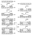
도 2a는 이 발명의 광학 필름의 제1 실시예의 횡단면도이다.
<도 2b>
도 2b는 이 발명의 광학 필름의 제2 실시예의 횡단면도이다.
<도 2c>
도 2c는 이 발명의 광학 필름의 제3 실시예의 횡단면도이다.
<도 2d>
도 2d는 이 발명의 광학 필름의 제4 실시예의 횡단면도이다.
<도 3>
도 3은 이 발명의 광학 결합층의 제1 실시예를 포함하는 조립체의 횡단면도이다.
<도 4>
도 4는 도 3에 예시된 광학 결합층을 이용하여 제1 기판과 제2 기판을 서로 결합하기 위한 공정도이다.
<도 5>
도 5는 이 발명의 광학 결합층의 제2 실시예를 포함하는 조립체의 횡단면도이다.
<도 6>
도 6은 도 5에 예시된 광학 결합층을 이용하여 제1 기판과 제2 기판을 서로 결합하기 위한 공정도이다.
<도 7>
도 7은 이 발명의 광학 결합층의 제3 실시예를 포함하는 조립체의 횡단면도이다.
<도 8>
도 8은 도 7에 예시된 광학 결합층을 이용하여 제1 기판과 제2 기판을 서로 결합하기 위한 공정도이다.
<도 9>
도 9는 이 발명의 광학 결합층의 제4 실시예를 포함하는 조립체의 횡단면도이다.
<도 10>
도 10은 도 9에 예시된 광학 결합층을 이용하여 제1 기판과 제2 기판을 서로 결합하기 위한 공정도이다.
<도 11>
도 11은 이 발명의 광학 결합층의 제5 실시예를 포함하는 조립체의 횡단면도이다.
<도 12>
도 12는 도 11에 예시된 광학 결합층을 이용하여 제1 기판과 제2 기판을 서로 결합하기 위한 공정도이다.≪ RTI ID =
1A is a top view of a substrate of the optical assembly of this invention.
≪ RTI ID = 0.0 &
1B is a perspective view of the substrate of FIG. 1A.
≪
2A is a cross sectional view of a first embodiment of an optical film of the present invention.
2b,
2B is a cross sectional view of a second embodiment of an optical film of the present invention.
Fig.
2C is a cross sectional view of a third embodiment of an optical film of the present invention.
Fig.
2D is a cross sectional view of a fourth embodiment of an optical film of the present invention.
3,
3 is a cross-sectional view of an assembly comprising a first embodiment of an optical coupling layer of this invention.
<Fig. 4>
FIG. 4 is a process diagram for bonding the first substrate and the second substrate to each other using the optical coupling layer illustrated in FIG. 3.
5,
5 is a cross sectional view of an assembly including a second embodiment of the optical coupling layer of the present invention.
6,
FIG. 6 is a process diagram for bonding the first substrate and the second substrate to each other using the optical coupling layer illustrated in FIG. 5.
7,
7 is a cross sectional view of an assembly including a third embodiment of the optical coupling layer of the present invention.
8,
FIG. 8 is a process diagram for bonding the first substrate and the second substrate to each other using the optical coupling layer illustrated in FIG. 7.
9,
9 is a cross-sectional view of an assembly including a fourth embodiment of the optical coupling layer of this invention.
<Fig. 10>
FIG. 10 is a process diagram for bonding the first substrate and the second substrate to each other using the optical coupling layer illustrated in FIG. 9.
11)
11 is a cross sectional view of an assembly including a fifth embodiment of the optical coupling layer of the present invention.
12,
FIG. 12 is a process diagram for bonding the first substrate and the second substrate to each other using the optical coupling layer illustrated in FIG. 11.
여기에 개시된 이 발명은 광학 결합층을 갖는 광학 조립체 및 광학 결합 방법을 기술한다. 광학 조립체는 광학 결합층으로 서로 결합되는 두개의 광학 기판을 포함한다. 광학 결합은 디스플레이에서 공기 틈을 제거함으로써, 향상된 일광 판독성(sunlight readability), 콘트라스트 및 휘도, 거칠기 및 큰 쇼크 및 진동에 대한 내성을 일으키면서, 디스플레이 성능을 향상시키고, 두개의 기판 사이의 응결 및 습기 집합을 제거할 수 있다. 이 발명의 광학 결합층은 광학상 투명한 액상 접착제(LOCA) 및 광학 필름을 포함한다. 광학 필름은 광학상 투명한 필름, 산광기 필름, 연신 가능한 광학상 투명한 또는 확산성 필름 등과 같은 접착제 또는 플라스틱 필름일 수 있을 것이다. LOCA는 광학상 투명한 또는 확산성 접착제와 같은 광학 품질을 갖는 복사 경화성 접착제일 수 있을 것이다. LOCA와 광학 필름의 조합은 광학 기판의 향상된 습윤 및 감소된 조립체 응력을 일으키고, 평행 및 비평행 기판들의 결합을 허용하고, 특정한 구조에서의 재작업성 및 제거성을 가능하게 한다.This invention disclosed herein describes an optical assembly having an optical coupling layer and an optical coupling method. The optical assembly includes two optical substrates bonded to each other with an optical coupling layer. Optical coupling eliminates air gaps in the display, resulting in improved sunlight readability, contrast and brightness, roughness and resistance to large shocks and vibrations, while improving display performance, condensation and moisture between the two substrates. You can remove a set. The optical coupling layer of this invention comprises an optically transparent liquid adhesive (LOCA) and an optical film. The optical film may be an adhesive or plastic film such as an optically transparent film, a diffuser film, a stretchable optically transparent or diffusing film, and the like. The LOCA may be a radiation curable adhesive having optical qualities such as an optically clear or diffusive adhesive. The combination of LOCA and optical film results in improved wetting and reduced assembly stress of the optical substrate, allows the bonding of parallel and non-parallel substrates, and enables reworkability and removal in certain structures.
이 발명의 예시적 조립체들은 제1 광학 기판과 제2 광학 기판 사이의 광학 결합을 제공하고 정상 사용 또는 특정한 업계 표준 가속된 노화 시험의 적용하에서 탈층하지 않는 광학 결합층에 의해 형성된다. 예를 들어, 이 발명의 조립체들은 섭씨 약 65도 또는 약 85도의 승온 저장 조건하에서 약 300 내지 약 1000시간의 기간 동안 탈층하지 않는다. 이 발명의 조립체들은 또한 예를 들어, 섭씨 약 65도 및 약 95% 상대 습도에 있는 가열 및 습도 저장의 조건하에서 약 300 내지 약 1000시간의 기간 동안 탈층하지 않는다.Exemplary assemblies of this invention are formed by an optical bonding layer that provides optical coupling between a first optical substrate and a second optical substrate and that does not delaminate under normal use or the application of certain industry standard accelerated aging tests. For example, the assemblies of this invention do not delaminate for a period of about 300 to about 1000 hours under elevated storage conditions of about 65 degrees Celsius or about 85 degrees Celsius. The assemblies of this invention also do not delaminate for a period of about 300 to about 1000 hours under conditions of heating and humidity storage at, for example, about 65 degrees Celsius and about 95% relative humidity.
광학 결합층은 성분을 거의 또는 전혀 손상시키지 않고 조립체가 재작업 되게 한다. 한 실시예에서는, 광학 결합층이, 성분을 거의 또는 전혀 손상시키지 않는 재작업성이 얻어질 수 있도록, 유리 기판들 사이에서 약 15N/㎜ 이하, 약 10N/㎜ 이하 및 약 6N/㎜ 이하의 분리 강도(cleavage strength)를 갖는다. 한 실시예에서는, 분리시키기 위한 총 에너지가 2.5 ㎝ × 2.5 ㎝의 면적에 대해 약 245.2 N (25 ㎏) 미만이다. 결합층은 연신 가능한 캐리어 필름의 연신 제거에 의해 재작업될 수 있을 것이다.The optical coupling layer allows the assembly to be reworked with little or no damage to the components. In one embodiment, the optical bonding layer is about 15 N / mm or less, about 10 N / mm or less and about 6 N / mm or less between the glass substrates so that reworkability can be obtained with little or no damage to the components. Has a cleavage strength. In one embodiment, the total energy to separate is less than about 245.2 N (25 kg) for an area of 2.5 cm × 2.5 cm. The bonding layer may be reworked by stretching removal of the stretchable carrier film.
광학 결합층은 어떤 적절한 두께든 가질 수 있을 것이다. 광학 조립체에 채택되는 특정한 두께는 다수의 요인에 의해 결정될 수 있을 것이다. 예를 들어, 광학 조립체가 이용되는 광학 장치의 설계는 광학 기판들 사이의 특정한 틈을 요구할 수 있을 것이다. 한 실시예에서는, 광학 결합층이 약 1 ㎛ 내지 약 12 ㎜, 약 1 ㎛ 내지 약 5 ㎜, 약 50 ㎛ 내지 약 2 ㎜, 약 50 ㎛ 내지 약 1 ㎜, 약 50 ㎛ 내지 약 0.5 ㎜ 또는 약 50 ㎛ 내지 약 0.2 ㎜의 두께를 갖는다.The optical coupling layer may have any suitable thickness. The particular thickness employed in the optical assembly may be determined by a number of factors. For example, the design of the optical device in which the optical assembly is used may require a specific gap between the optical substrates. In one embodiment, the optical coupling layer has a thickness of about 1 μm to about 12 mm, about 1 μm to about 5 mm, about 50 μm to about 2 mm, about 50 μm to about 1 mm, about 50 μm to about 0.5 mm, or about Have a thickness of 50 μm to about 0.2 mm.
이 발명의 접착제는, 25 ㎛ 두께의 시료 상에서 아래에 기술된 방식으로 측정됨에 따라 약 75% 이상의 광학 투과 및 약 10% 미만의 탁도 값을 나타내면, 광학상 투명한 것으로 간주된다. 광학 결합층은 의도된 응용분야를 위해 적절한 광학 성질을 갖는다. 예를 들어, 광학 결합층은 약 400 내지 약 720 ㎚의 범위에 걸쳐 약 85% 이상의 투과율을 가질 수 있을 것이다. 광학 결합층은 밀리미터 두께 당, 460 ㎚에서 약 85% 초과, 530 ㎚에서 약 90% 초과 및 670 ㎚에서 약 90% 초과의 투과를 가질 수 있을 것이다. 한 실시예에서는, 광학 결합층이, 상온 및 제어된 습도 조건(CTH)(controlled humidity conditions)에서 30일 후에, 약 80% 이상, 특별하게는 약 85% 이상 및 더 특별하게는 약 88% 이상의 투과 비율을 갖는다. 다른 한 실시예에서는, 광학 결합층이, 65℃ 및 90% 상대 습도에서의 열 노화의 30일 후에, 약 75% 이상, 특별하게는 약 77.5% 이상 및 더 특별하게는 약 80% 이상의 투과 비율을 갖는다. 또다른 한 실시예에서는, 광학 결합층이, 70℃에서의 열 노화의 30일 후에, 약 75% 이상, 특별하게는 약 77.5% 이상 및 더 특별하게는 약 80% 이상의 투과 비율을 갖는다. 이러한 투과 특성은, 광학 조립체가 풀 컬러 디스플레이(full color display)에 이용되는 경우에 색점(color point)을 유지하기에 중요한, 전자기적 스펙트럼의 가시 구역에 걸쳐 균일한 광투과를 제공한다. 광학 결합층은 특히, 제1 광학 기판 및/또는 제2 광학 기판의 굴절률에 맞추거나 또는 거의 맞추는 굴절률을 갖는다. 한 실시예에서는, 광학 결합층이 약 1.4 내지 약 1.6의 굴절률을 갖는다.Adhesives of this invention are considered to be optically transparent if they exhibit an optical transmission of at least about 75% and a haze value of less than about 10% as measured in the manner described below on a 25 μm thick sample. The optical coupling layer has optical properties suitable for the intended application. For example, the optical coupling layer may have a transmission of at least about 85% over a range of about 400 to about 720 nm. The optical coupling layer may have a transmission of greater than about 85% at 460 nm, greater than about 90% at 530 nm and greater than about 90% at 670 nm per millimeter thickness. In one embodiment, the optical coupling layer is at least about 80%, particularly at least about 85% and more particularly at least about 88% after 30 days at room temperature and controlled humidity conditions (CTH) Has a transmission ratio. In another embodiment, the optical coupling layer has a transmission rate of at least about 75%, particularly at least about 77.5% and more particularly at least about 80% after 30 days of thermal aging at 65 ° C. and 90% relative humidity. Has In another embodiment, the optical coupling layer has a transmission ratio of at least about 75%, particularly at least about 77.5% and more particularly at least about 80% after 30 days of thermal aging at 70 ° C. This transmission characteristic provides uniform light transmission over the visible region of the electromagnetic spectrum, which is important for maintaining color points when the optical assembly is used in a full color display. The optical coupling layer in particular has a refractive index that matches or nearly matches the refractive index of the first optical substrate and / or the second optical substrate. In one embodiment, the optical coupling layer has a refractive index of about 1.4 to about 1.6.
또다른 한 실시예에서는, 광학 필름 및/또는 LOCA가 확산성, 색 보정성, UV 흡수(-400 ㎚ 미만의 광투과의 차단) 및 IR 흡수(800 ㎚ 초과의 광투과의 차단) 등을 가질 수 있을 것이다.In another embodiment, the optical film and / or LOCA have diffusivity, color correction, UV absorption (blocking light transmission below -400 nm), IR absorption (blocking light transmission above 800 nm), and the like. Could be.
이 발명의 광학 조립체들은 제1 기판과 제2 기판 사이에 배치된 광학 결합층을 포함한다. 이 방법을 이용하여 어떤 적절한 투명 광학 기판이든 결합될 수 있다. 한 실시예에서는, 광학 기판이 디스플레이 패널 및 사실상 광투과성인 기판을 포함한다.Optical assemblies of this invention include an optical coupling layer disposed between a first substrate and a second substrate. Using this method any suitable transparent optical substrate can be combined. In one embodiment, the optical substrate comprises a display panel and a substrate that is substantially light transmissive.
광학 기판은 유리, 중합체, 합성물 등으로 형성될 수 있을 것이다. 광학 기판을 위해 이용되는 재료의 유형은 일반적으로 조립체가 이용될 것인 응용분야에 의존한다.The optical substrate may be formed of glass, polymer, composite or the like. The type of material used for the optical substrate generally depends on the application in which the assembly will be used.
적절한 광학 기판은 어떤 영율(Young's modulus)로든 될 수 있고, 예를 들어, 딱딱하거나(예를 들어, 광학 기판은 6 밀리미터 두께의 평판 유리 시트일 수 있을 것임) 또는 유연할(예를 들어, 광학 기판은 37 마이크로미터 두께의 폴리에스테르 필름일 수 있을 것임) 수 있을 것이다.Suitable optical substrates may be at any Young's modulus, and may be, for example, rigid (eg, the optical substrate may be a 6 mm thick flat glass sheet) or flexible (eg, optical The substrate may be a polyester film 37 micrometers thick).
재료 유형과 마찬가지로, 광학 기판의 크기 및 표면 형태는 일반적으로 광학 조립체가 이용될 것인 응용분야에 의존한다. 광학 기판의 표면 형태는 거칠어질 수도 있을 것이다. 거친 표면 형태를 갖는 광학 기판은 이 발명에 따라 효과적으로 적층될 수 있다.As with the type of material, the size and surface shape of the optical substrate generally depend on the application in which the optical assembly will be used. The surface shape of the optical substrate may be rough. Optical substrates having a rough surface form can be effectively laminated according to this invention.
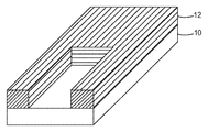
도 1a 및 도 1b는 기판(10)이 갖는 표면 형태의 한 예의 상면도 및 투시도를 각각 도시한다. 도 1a 및 도 1b에 도시된 바와 같이, 한 실시예에서는, 기판(10)이 세개의 엣지에서 테이프(12)로 마스크(mask) 되는 유리로 만들어진다. 한 실시예에서는, 테이프가 3Mㄾ Vinyl Tape 471이다. 기판(10) 상에 배치되는 테이프(12)의 형상으로 인해, 기판(10)은 두개의 상이한 높이를 갖는다. 제1 높이는 유리 기판의 높이에 대응하고, 제2 높이는 유리 기판과 비닐 테이프의 조합된 높이에 대응한다. 두개의 변하는 높이는 기판(10)의 표면 상에, 유리 또는 플라스틱 커버 렌즈 상에 인쇄되는 잉크 스텝과 유사한, 표면 형태를 생성한다.1A and 1B show top and perspective views, respectively, of an example of the surface shape of
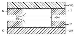
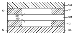
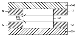
광학 결합층은 LOCA와 광학 필름의 변하는 조합을 포함할 수 있다. 제1 실시예에서는, 광학 결합층이 LOCA 및 광학 필름을 포함한다(도 3 및 도 9). 제2 실시예에서는, 광학 결합층이 제1 LOCA, 제2 LOCA 및 제1 LOCA와 제2 LOCA 사이에 배치된 광학 필름을 포함한다(도 5, 도 7 및 도 11).The optical coupling layer can comprise varying combinations of LOCA and optical film. In the first embodiment, the optical coupling layer comprises a LOCA and an optical film (FIGS. 3 and 9). In a second embodiment, the optical coupling layer comprises a first LOCA, a second LOCA, and an optical film disposed between the first LOCA and the second LOCA (FIGS. 5, 7, and 11).
LOCA 층은 고가의 진공 적층기 및/또는 오토클레이브를 필요로 하지 않고 기판에 대한 필름 접착제의 무기포 적층이 가능하게 한다. LOCA 층은, 어떤 높이 차이든 메우는 것에 도움이 될 수도 있으며, 그렇지 않으면 기판과 필름 접착제 사이의 탈층 또는 기포 형성을 유발할 수 있을 것이다. 광학 결합층이 광학 필름을 포함하기도 하기 때문에, 더 적은 총량의 LOCA가 필요하고, LOCA가 경화함에 따른 기판 상의 열부하(heat load)를 최소화한다.The LOCA layer enables inorganic lamination of film adhesive to the substrate without the need for expensive vacuum laminators and / or autoclaves. The LOCA layer may help to fill in any height difference, otherwise it may cause delamination or bubble formation between the substrate and the film adhesive. Since the optical coupling layer also includes an optical film, a smaller total amount of LOCA is required, minimizing heat load on the substrate as the LOCA cures.
LOCA는 광학상 투명한 액상 접착제, 산광 접착제, 색 보정 접착제 또는 큰 광학 조립체의 효율적 제조를 위해 적절한 점도를 갖는 액체 조성물이다. 큰 광학 조립체는 약 15 ㎠ 내지 약 5㎡ 또는 약 15 ㎠ 내지 약 1 ㎡의 면적을 가질 수 있을 것이다. 예를 들어, 액체 조성물은, 25℃에서 조성물에 대한 점도가 측정되는 경우에, 약 100 내지 약 10,000cp, 약 200 내지 약 1000cp, 약 200 내지 약 700cp, 또는 약 200 내지 약 500cp의 점도를 가질 수 있을 것이다. 액체 조성물은 다양한 제조 방법에 사용하기에 적합하다. 적절한 LOCA의 예는, 제한적인 것은 아니지만, 고율 및 고점착 폴리우레탄 접착제 및 저율 및 저점착 우레탄 아크릴레이트 접착제를 포함한다. 적절한 구입 가능한 고율 및 고점착 폴리우레탄 접착제의 예는, 제한적인 것은 아니지만, LOCA 2175를 포함한다. 적절한 저율 및 저점착 우레탄 아크릴레이트 접착제의 예는, 제한적인 것은 아니지만, LOCA 2312를 포함한다. 둘다 미국, 미네소타, 세인트 폴에 소재하는 쓰리엠 컴퍼니(3M Company)로부터 구입 가능하다.LOCA is a liquid composition having an appropriate viscosity for the efficient manufacture of optically clear liquid adhesives, diffuser adhesives, color correction adhesives or large optical assemblies. Large optical assembly is about 15
일반적으로, "경화성"은 열, 어떤 유형의 복사 또는 에너지를 가하는 것과 같은 예정된 조건하에서, 또는 상온에서 두개의 반응성 성분을 단순히 조합함으로써 경화시키는 조성물, 층, 구역 등을 기술하기 위해 이용된다. 여기에서 이용되는, "경화성"은, (1) 사실상 비경화되고(즉, 약 50% 이하의 반응성 단량체가 중합화됨) 단지 부분적으로 경화되거나 또는 사실상 완전히 경화된(즉, 50% 초과의 단량체가 중합화됨) 조성물, 층 또는 구역; 또는 (2) 부분적으로 경화되고 부분적으로 비경화되며, 적어도 비경화된 부분의 일부의 양이 경화된 조성물, 층 또는 구역; 또는 (3) 사실상 비경화되고 적어도 부분적으로 경화되거나 또는 사실상 완전히 경화된 조성물, 층 또는 구역을 기술하기 위해 이용된다.In general, "curable" is used to describe compositions, layers, zones, and the like that cure under predetermined conditions, such as applying heat, any type of radiation or energy, or by simply combining two reactive components at room temperature. As used herein, “curable” means that (1) virtually uncured (ie, up to about 50% of the reactive monomers are polymerized) and only partially cured or substantially completely cured (ie, greater than 50% of monomers). Polymerized) composition, layer or zone; Or (2) a composition, layer or zone that is partially cured and partially uncured, and wherein the amount of at least a portion of the uncured portion is cured; Or (3) to describe a composition, layer or zone that is substantially uncured and at least partially cured or substantially fully cured.
경화 수단 중 어느 하나 또는 조합이 LOCA를 경화시키기 위해 이용될 수 있을 것이다. 예를 들어, UV 복사(200-400 ㎚), 화학선 복사(700 ㎚ 이하), 근적외선(near-IR) 복사(700-1500 ㎚), 가열 및 전자빔(electron beam) 또는 그들의 어떤 조합이든 이용될 수 있을 것이다. 광학 기판들 중 하나 또는 둘다가 화학선 복사의 투과를 허용하지 않는 경계를 갖는 것을 제외하고, 예를 들어, 경화성 층을 경화시키기 위해 화학선 복사를 이용하는 것이 바람직하다면, 경화 수단의 조합이 유용할 수 있을 것이다. 이 경우에, 경계로 인해 화학선 복사가 접근할 수 없는 경화성 층을 경화시키기 위해 가열이 이용될 수 있을 것이다.Any one or combination of curing means may be used to cure the LOCA. For example, UV radiation (200-400 nm), actinic radiation (700 nm or less), near-IR (near-IR) radiation (700-1500 nm), heating and electron beam or any combination thereof may be used. Could be. Combinations of curing means would be useful if, for example, one or both of the optical substrates had boundaries that would not allow transmission of actinic radiation, for example, if it would be desirable to use actinic radiation to cure the curable layer. Could be. In this case, heating may be used to cure the curable layer due to the boundary where actinic radiation is inaccessible.
광학 필름은 광학 기판 중 하나 또는 LOCA 층 상에 직접 도포된다. 어떤 적절한 광학 필름 또는 광학 필름 접착제든 이 발명을 위해 이용될 수 있다. 예를 들어, 광학 필름은, 제한적인 것은 아니지만, 광학상 투명한 필름 접착제, 연신 이형 가능한 광학상 투명한 접착제 및 연신 이형 가능한 캐리어 필름(stretch releasable carrier film)을 포함할 수 있다. 한 실시예에서는, 광학 필름이 광학상 투명한 접착제(OCA) 필름이다. 이러한 OCA 필름은 광학 조립체를 위해 이용하기 쉽고 전형적으로 이미 중합화 되어 있다. 선택적 가교(crosslinking) 또는 경화후(postcuring) 단계가 OCA의 응집성을 더 강화시키기 위해 이용될 수도 있을 것이다. 한 실시예에서는, 광학 필름 접착제가 감압성 접착제이다. 감압성 접착제(PSA)는, (1) 매우 강하고 한층 더 영구적인 점착, (2) 손가락 압력을 초과하지 않는 압력으로 기판에 부착, (3) 부착물 상에의 충분한 유지 능력, 및/또는 (4) 부착물로부터 깨끗하게 제거되기에 충분한 응집 강도와 같은 성질을 갖는 것으로 알려져 있다. 광학 필름 또는 광학 필름 접착제는 디스플레이 기판들 사이의 메워질 공기 공동 또는 틈의 유의미한 부분을 점유하고, 그래서, 액체 접착제의 요구 체적을 줄이며, 그것은 총 광학 결합층의 유효 수축을 저감시키고, 조립체에서의 총 응력의 저감을 일으키며, 무라 결함(Mura defects)의 확률을 저감시킨다. 예시적 적절한 필름 접착제는, 제한적인 것은 아니지만, 폴리비닐 에테르 폴리우레탄, 실리콘, 및 폴리(메트)아크릴레이트(아크릴레이트 및 메타크릴레이트를 모두 포함)를 포함한다.The optical film is applied directly onto one of the optical substrates or the LOCA layer. Any suitable optical film or optical film adhesive may be used for this invention. For example, the optical film may include, but is not limited to, an optically clear film adhesive, a stretchable optically clear adhesive, and a stretch releasable carrier film. In one embodiment, the optical film is an optically clear adhesive (OCA) film. Such OCA films are easy to use for optical assemblies and are typically already polymerized. An optional crosslinking or postcuring step may be used to further enhance the cohesiveness of the OCA. In one embodiment, the optical film adhesive is a pressure sensitive adhesive. Pressure-sensitive adhesives (PSAs) are (1) very strong and even more permanent adhesion, (2) adhere to the substrate at a pressure not exceeding finger pressure, (3) sufficient retention ability on the deposit, and / or (4 It is known to have properties such as sufficient cohesive strength to be removed cleanly from the deposit. The optical film or optical film adhesive occupies a significant portion of the air cavity or gap to be filled between the display substrates, thus reducing the required volume of the liquid adhesive, which reduces the effective shrinkage of the total optical bonding layer, and It reduces the total stress and reduces the probability of Mura defects. Exemplary suitable film adhesives include, but are not limited to, polyvinyl ether polyurethane, silicone, and poly (meth) acrylates (including both acrylates and methacrylates).
폴리(메트)아크릴레이트 필름 접착제는 알킬(메트)아크릴레이트와 같은 단량체로부터 준비될 수 있을 것이다. 유용한 알킬(메트)아크릴레이트(즉, 아크릴산 알킬 에스테르 단량체)는 선형 또는 분지형 단일작용성 아크릴레이트 또는 비-3차 알킬 알코올의 메타크릴레이트, 1 내지 14개 및 특정하게는, 1 내지 12개의 탄소 원자를 갖는 알킬 그룹을 포함한다. 유용한 단량체에는 부틸 (메트)아크릴레이트, 2-에틸헥실 (메트)아크릴레이트, 에틸 (메트)아크릴레이트, 메틸 (메트)아크릴레이트, n-프로필 (메트)아크릴레이트, 아이소프로필 (메트)아크릴레이트, 펜틸 (메트)아크릴레이트, n-옥틸 (메트)아크릴레이트, 아이소옥틸 (메트)아크릴레이트, 아이소노닐 (메트)아크릴레이트 및 2-메틸-부틸 (메트)아크릴레이트가 포함된다.Poly (meth) acrylate film adhesives may be prepared from monomers such as alkyl (meth) acrylates. Useful alkyl (meth) acrylates (ie, acrylic acid alkyl ester monomers) are methacrylates, 1 to 14 and specifically 1 to 12, of linear or branched monofunctional acrylates or non-tertiary alkyl alcohols. Alkyl groups having carbon atoms. Useful monomers include butyl (meth) acrylate, 2-ethylhexyl (meth) acrylate, ethyl (meth) acrylate, methyl (meth) acrylate, n-propyl (meth) acrylate, isopropyl (meth) acrylate , Pentyl (meth) acrylate, n-octyl (meth) acrylate, isooctyl (meth) acrylate, isononyl (meth) acrylate and 2-methyl-butyl (meth) acrylate.
한 실시예에서는, 광학 필름이 하나 이상의 폴리(메트)아크릴레이트(예를 들어, (메트)아크릴 감압성 접착제)를 기초로 한다. 폴리(메트)아크릴레이트 접착제는, 예를 들어, 아이소옥틸 아크릴레이트(IOA), 아이소노닐 아크릴레이트, 2-메틸-부틸 아크릴레이트, 2-에틸-헥실 아크릴레이트 및 n-부틸 아크릴레이트, 아이소부틸 아크릴레이트, 헥실 아크릴레이트, n-옥틸 아크릴레이트, n-옥틸 메타크릴레이트, n-노닐 아크릴레이트, 아이소아밀 아크릴레이트, n-데실 아크릴레이트, 아이소데실 아크릴레이트, 아이소데실 메타크릴레이트, 및 도데실 아크릴레이트와 같은 하나 이상의 알킬(메트)아크릴레이트 에스테르 단량체; 및 예를 들어, (메트)아크릴산, N-비닐 피롤리돈, N-비닐카프롤락탐, N,N-di메틸(메트)아크릴아미드, N-아이소피로필(메트)아크릴아미드, (메트)아크릴아미드, 아이소보닐 아크릴레이트, 4-메틸-2-펜틸 아크릴레이트, 하이드록시알킬(메트)아크릴레이트, 비닐 에스테르, 폴리스티렌 또는 폴리메틸 메타크릴레이트 거대단량체, 알킬 말레이트 및 알킬 푸마레이트(제각기, 말레인산 및 푸마르산을 기초로 함), 또는 그 조합과 같은 하나 이상의 선택적 공단량체 성분으로부터 파생된다.In one embodiment, the optical film is based on one or more poly (meth) acrylates (eg, (meth) acrylic pressure sensitive adhesives). Poly (meth) acrylate adhesives include, for example, isooctyl acrylate (IOA), isononyl acrylate, 2-methyl-butyl acrylate, 2-ethyl-hexyl acrylate and n-butyl acrylate, Isobutyl acrylate, hexyl acrylate, n-octyl acrylate, n-octyl methacrylate, n-nonyl acrylate, isoamyl acrylate, n-decyl acrylate, isodecyl acrylate, isodecyl methacrylate, And one or more alkyl (meth) acrylate ester monomers such as dodecyl acrylate; And for example, (meth) acrylic acid, N-vinyl pyrrolidone, N-vinyl caprolactam, N, N-dimethyl (meth) acrylamide, N-isopyrophyll (meth) acrylamide, (meth) Acrylamide, isobornyl acrylate, 4-methyl-2-pentyl acrylate, hydroxyalkyl (meth) acrylate, vinyl ester, polystyrene or polymethyl methacrylate macromonomer, alkyl malate and alkyl fumarate (each Based on maleic acid and fumaric acid), or combinations thereof.
다른 실시예에서, 폴리(메트)아크릴 필름 접착제는, 약 0과 약 40 중량 퍼센트(wt%) 사이의 하이드록시알킬(메트)아크릴레이트 및 약 100wt%와 약 60wt% 사이의 아이소옥틸 아크릴레이트, 2-에틸-헥실 아크릴레이트 또는 n-부틸 아크릴레이트 중 하나 이상의 조성물로부터 파생될 수 있다. 하이드록시에틸(메트)아크릴레이트는 40%, 30%, 20%, 10%까지 일 수 있고, 잔부는 아이소옥틸아크릴레이트, 2-에틸헥실아크릴레이트, 부틸아크릴레이트, 아이소보닐 아크릴레이트 등과 같은 알킬아크릴레이트이다. 다른 한 실시예에서, 하이드록시알킬(메트)아크릴레이트는 아크릴산(총 (메트)아크릴레이트 조성물의 15%까지)으로 치환될 수 있다. 하나의 특정한 실시예는, 약 1wt%와 약 2wt% 사이의 하이드록시알킬(메트)아크릴레이트 및 약 99wt%와 약 98wt% 사이의 아이소옥틸 아크릴레이트, 2-에틸헥실 아크릴레이트 또는 n-부틸 아크릴레이트 중 하나 이상의 조성물로부터 파생될 수 있다. 다른 특정한 실시예는, 약 1wt% 내지 약 2wt%의 하이드록시알킬(메트)아크릴레이트 및 약 99wt% 내지 약 98wt%의 n-부틸 아크릴레이트와 메틸 아크릴레이트의 조합의 조성물로부터 파생될 수 있다.In another embodiment, the poly (meth) acrylic film adhesive comprises between about 0 and about 40 weight percent (wt%) of hydroxyalkyl (meth) acrylate and between about 100 wt% and about 60 wt% isooctyl acrylate , 2-ethyl-hexyl acrylate or n-butyl acrylate. The hydroxyethyl (meth) acrylate may be up to 40%, 30%, 20%, 10%, the balance isooctyl acrylate, 2-ethylhexyl acrylate, butyl acrylate, isobornyl acrylate and the like. Same alkyl acrylate. In another embodiment, hydroxyalkyl (meth) acrylate can be substituted with acrylic acid (up to 15% of the total (meth) acrylate composition). One particular embodiment comprises between about 1 wt% and about 2 wt% hydroxyalkyl (meth) acrylate and between about 99 wt% and about 98 wt% isooctyl acrylate, 2-ethylhexyl acrylate or n-butyl It may be derived from one or more compositions of acrylates. Another particular embodiment may be derived from a composition of a combination of about 1 wt% to about 2 wt% hydroxyalkyl (meth) acrylate and about 99 wt% to about 98 wt% of n-butyl acrylate and methyl acrylate.
제한적인 것은 아니지만, 오일, 가소제, 항산화제, UV 안정제, 안료, 경화제, 중합체 첨가제, 농조화제, 염료, 사슬 전달제 및 다른 첨가제를 포함하는, 다양한 기능 재료들은, 그들이 필름 접착제의 광학 투명도를 현저히 저감시키지 않는다면, 첨가될 수도 있다.Although not limiting, various functional materials, including oils, plasticizers, antioxidants, UV stabilizers, pigments, hardeners, polymer additives, thickeners, dyes, chain transfer agents and other additives, significantly reduce the optical transparency of film adhesives. If not reduced, it may be added.
선택적으로, 광학 필름은, 연신 이형 가능한 광학상 투명한 접착제(SROCA)(stretch releasable optically clear adhesive) 및/또는 연신 이형 성질을 갖는 캐리어 필름, 즉 연신 이형 가능한 캐리어 필름(SRCF)(stretch releasable carrier film)을 포함할 수 있을 것이다. 연신 가능한 층은 LOCA 층과 기판의 사이, 또는 LOCA 층들의 사이에 삽입될 수 있다. SROCA 또는 SRCF의 첨가는, 디스플레이의 쉬운 조립 및 분해를 허용하면서, 조립의 재작업이 가능하게 한다. 적절한 SROCA의 예는, 미국 특허출원 공보 2009/0229732 A1호, 2011/0126968 A1호 및 2011/0253301 A1호에 기술되어 있다.Optionally, the optical film may be a carrier film having a stretch releasable optically clear adhesive (SROCA) and / or stretch release properties, ie a stretch releasable carrier film (SRCF). It may include. The stretchable layer may be inserted between the LOCA layer and the substrate, or between the LOCA layers. The addition of SROCA or SRCF allows for rework of the assembly while allowing easy assembly and disassembly of the display. Examples of suitable SROCA are described in US Patent Application Publications 2009/0229732 A1, 2011/0126968 A1, and 2011/0253301 A1.
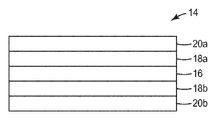
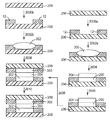
도 2a 내지 도 2d는 이 발명의 광학 결합층의 다양한 구조의 예를 제공한다. 도 2a는 제1 OCA(18a)와 제2 OCA(18b) 사이에 배치된 캐리어 필름(16)을 포함하는 광학 필름(14)의 전체 구조의 횡단면도를 도시한다. 전체 구조는 연신 이형 가능한 캐리어 필름(16)이 사이에 있는 두개의 OCA 층을 포함한다. 이형 라이너(22a 및 22b)는 OCA(18a, 18b)의 표면 상에 제각기 배치되어 사용 대기하기까지 청결을 유지한다.2A-2D provide examples of various structures of the optical coupling layer of this invention. 2A shows a cross-sectional view of the overall structure of an
도 2b는 OCA(26) 및 캐리어 필름(28)을 포함하는 광학 필름(24)의 절반 구조의 횡단면도를 도시한다. 이형 라이너(30)는 OCA(26)에 인접하게 배치되어 사용 대기하기까지 청결을 유지한다. 프리마스크 라이너(premask liner)(32)는 캐리어 필름(28)에 인접하게 배치되고, 표면이 입자, 섬유 등으로 오염되는 것을 방지하기도 한다.2B shows a cross-sectional view of a half structure of an
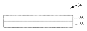
도 2c에 도시된 또다른 실시예에서는, 광학 결합층의 광학 필름(34)이 연신 이형 가능한 캐리어 필름(SRCF)(36)만을 포함한다. 프리마스크 라이너(38)는 캐리어 필름(36)에 인접하게 배치된다.In another embodiment shown in FIG. 2C, the
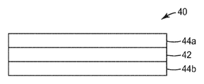
도 2d는 이형 라이너(44a 및 44b) 사이에 배치된 OCA(42)만을 포함하는 광학 필름(40)의 횡단면도를 도시한다.FIG. 2D shows a cross-sectional view of
이 발명의 광학 결합층은 예를 들어, 액정 디스플레이 패널, OLED 디스플레이 패널, 및 플라즈마 디스플레이 패널인 광범위한 디스플레이 패널에 대한 투명한 오버레이의 용도에 유용하다.The optical coupling layer of this invention is useful for the use of transparent overlays for a wide range of display panels, for example liquid crystal display panels, OLED display panels, and plasma display panels.
어떤 실시예에서는, 광학 조립체가 액정 디스플레이 조립체를 포함하며, 디스플레이 패널은 액정 디스플레이 패널을 포함한다. 액정 디스플레이 패널은 잘 알려져 있으며, 전형적으로 유리 또는 중합체 기판과 같은 2개의 사실상 투명한 기판들 사이에 배치된 액정 재료를 포함한다. 여기에서 이용되는, '사실상 투명한'은, 밀리미터 두께 당, 400 ㎚에서 약 85% 초과, 530 ㎚에서 약 90% 초과, 및 670 ㎚에서 약 90% 초과의 투과를 갖는 기판을 지칭한다. 사실상 투명한 기판의 내부 표면 상에는, 전극으로서 기능하는 투명한 전기 전도성 물질이 있다. 일부 경우에, 사실상 투명한 기판의 외부 표면 상에는, 본질적으로 광의 단지 하나의 편광 상태만을 통과시키는 편광 필름이 있다. 이 전극을 가로질러 전압이 선택적으로 인가될 때, 액정 재료는 재배향되어 광의 편광 상태를 변경시켜서 이미지가 생성되게 된다. 액정 디스플레이 패널은, 매트릭스 패턴(matrix pattern)으로 배열된 복수의 TFT를 갖는 박막 트랜지스터(TFT) 어레이 패널(thin film transistor array panel)과 공통 전극을 갖는 공통 전극 패널 사이에 배치된, 액정 재료를 포함할 수도 있다.In some embodiments, the optical assembly comprises a liquid crystal display assembly, and the display panel comprises a liquid crystal display panel. Liquid crystal display panels are well known and typically comprise a liquid crystal material disposed between two substantially transparent substrates, such as glass or polymer substrates. As used herein, 'virtually transparent' refers to a substrate having a transmission of greater than about 85% at 400 nm, greater than about 90% at 530 nm, and greater than about 90% at 670 nm per millimeter thickness. On the inner surface of a substantially transparent substrate, there is a transparent electrically conductive material that functions as an electrode. In some cases, on the outer surface of a substantially transparent substrate there is a polarizing film that essentially passes only one polarization state of light. When a voltage is selectively applied across this electrode, the liquid crystal material is redirected to change the polarization state of the light to produce an image. The liquid crystal display panel includes a liquid crystal material disposed between a common electrode panel having a thin film transistor array panel (TFT) array panel having a plurality of TFTs arranged in a matrix pattern and a common electrode You may.
어떤 실시예에서, 광학 조립체는 플라즈마 디스플레이 조립체를 포함하고, 디스플레이 패널은 플라즈마 디스플레이 패널을 포함한다. 플라즈마 디스플레이 패널은 공지되어 있고, 전형적으로 두개의 유리 패널 사이에 있는 많은 작은 셀(tiny cell) 속에 배치된 네온 및 제논과 같은 희귀 기체들의 불활성 혼합물을 포함한다. 패널 내의 제어 회로 전하 전극은 이들 기체를 이온화시키고 플라즈마를 형성시키며, 이어서 이 플라즈마는 인광체(phosphor)를 여기시켜 광을 방출한다.In some embodiments, the optical assembly comprises a plasma display assembly and the display panel comprises a plasma display panel. Plasma display panels are known and typically comprise an inert mixture of rare gases such as neon and xenon disposed in many tiny cells between two glass panels. The control circuit charge electrodes in the panel ionize these gases and form a plasma, which in turn excites the phosphor to emit light.
어떤 실시예에서, 광학 조립체는 유기 전기발광 조립체를 포함하고, 디스플레이 패널은 두개의 유리 패널 사이에 배치된 유기 발광 다이오드 또는 발광 중합체를 포함한다.In some embodiments, the optical assembly comprises an organic electroluminescent assembly and the display panel comprises an organic light emitting diode or light emitting polymer disposed between the two glass panels.
예를 들어, 전자 종이 디스플레이에서 이용되는 것 등과 같은 터치 패널을 갖는 전기영동 디스플레이와 같은 다른 유형의 디스플레이 패널들이 디스플레이 결합에서 유리할 수도 있다.For example, other types of display panels, such as electrophoretic displays with touch panels such as those used in electronic paper displays, may be advantageous in display combinations.
광학 조립체는, 밀리미터 두께 당, 400 ㎚에서 약 85% 초과, 530 ㎚에서 약 90% 초과, 및 670 ㎚에서 약 90% 초과의 투과율을 갖는 사실상 투명한 기판을 포함하기도 한다. 전형적인 액정 디스플레이 조립체에서, 사실상 투명한 기판은 전면 또는 후면 커버 플레이트로 지칭될 수 있다. 사실상 투명한 기판은 유리 또는 중합체를 포함할 수도 있다. 유용한 유리에는 보로실리케이트, 소다석회, 및 보호 커버로서 디스플레이 응용에 사용하기에 적합한 다른 유리가 포함된다. 유용한 중합체는, 제한적인 것은 아니지만, 제온 케미컬 엘.피.(Zeon Chemicals L.P.)로부터 구입 가능한 Zeonox 및 Zeonor와 같은, PET와 같은 폴리에스테르 필름, 폴리카보네이트 필름 또는 플레이트, 아크릴 플레이트 및 사이클로올레핀 중합체를 포함한다. 사실상 투명한 기판은 특히 디스플레이 패널 및/또는 광중합성 층의 굴절률에 근접하는 굴절률을 갖는다. 예를 들어, 약 1.45와 약 1.55 사이이다. 사실상 투명한 기판은 전형적으로 두께가 약 0.5 내지 약 5 ㎜이다.The optical assembly also includes a substantially transparent substrate having a transmission of more than about 85% at 400 nm, more than about 90% at 530 nm, and more than about 90% at 670 nm per millimeter thickness. In a typical liquid crystal display assembly, a substantially transparent substrate may be referred to as a front or back cover plate. A substantially transparent substrate may comprise glass or polymer. Useful glasses include borosilicates, soda lime, and other glasses suitable for use in display applications as protective covers. Useful polymers include, but are not limited to, polyester films such as PET, polycarbonate films or plates, acrylic plates and cycloolefin polymers, such as Zeonox and Zeonor, available from Zeon Chemicals LP. do. A substantially transparent substrate has a refractive index that is close to the refractive index of the display panel and / or photopolymerizable layer in particular. For example, between about 1.45 and about 1.55. Virtually transparent substrates are typically about 0.5 to about 5 mm thick.
어떤 실시예에서는, 사실상 투명한 기판이 터치 스크린을 포함한다. 터치 스크린은 이 기술 분야에서 공지되어 있고, 일반적으로 두개의 사실상 투명한 기판 사이에 배치된 투명한 전도성 층을 포함한다. 예를 들어, 터치 스크린은 유리 기판과 중합체 기판 사이에 배치된 인듐/주석 산화물을 포함할 수 있을 것이다.In some embodiments, the substantially transparent substrate comprises a touch screen. Touch screens are known in the art and generally comprise a transparent conductive layer disposed between two substantially transparent substrates. For example, the touch screen may include indium / tin oxide disposed between the glass substrate and the polymer substrate.
예Yes
본 발명은, 본 발명의 범주 내에 있는 많은 변형 및 변경이 당업자에게는 명백할 것이기 때문에 단지 예시로서 의도된 하기의 예에서 더욱 상세하게 설명된다. 달리 언급되지 않는다면, 하기 예에서 보고된 모든 부, 백분율, 및 비는 중량 기준이다.The present invention is described in further detail in the following examples, which are intended as illustrations only, since many variations and modifications within the scope of the present invention will be apparent to those skilled in the art. Unless otherwise stated, all parts, percentages, and ratios reported in the following examples are by weight.

시험 방법Test Methods
탁도 및 투과율Turbidity and transmittance
미국, 버지니아, 레스턴 소재의 헌터랩(HunterLab)으로부터 구입 가능한 Hunter Ultrascan PRO, 모델 USP 1469를 이용하여 탁도(%) 및 투과율(%)이 측정되었다.Turbidity (%) and transmittance (%) were measured using Hunter Ultrascan PRO, model USP 1469, available from HunterLab, Reston, Va., USA.
연신Stretching 이형력( Release force ( SRFSRF ))
미국, 매사추세츠, 캔턴 소재의 인스트론 코포레이션(Instron Corporation)으로부터 구입 가능한 인장력 시험기 모델 번호 5500을 이용하여 시험이 수행되었다. 인스트론 코포레이션으로부터 구입 가능한 500 Newton 로드셀이 이용되었다. 시험은 12 in/min(30.5 ㎝/min)의 신장율(extension rate)로 수행되었다. 인장력 시험기의 하부 턱이 연신 이형 재료 탭의 반대쪽의 광학 조립체의 엣지를 붙잡는다. 시험기의 상부 턱이 광학 조립체의 연신 이형 탭을 붙잡는다.Testing was performed using a tensile tester model number 5500, available from Instron Corporation of Canton, Massachusetts, USA. A 500 Newton load cell, available from Instron Corporation, was used. The test was performed at an extension rate of 12 in / min (30.5 cm / min). The lower jaw of the tensile force tester holds the edge of the optical assembly opposite the tab of the stretch release material. The upper jaw of the tester grips the stretched release tab of the optical assembly.
접착제의 준비Preparation of the glue
SROCA1의 준비Preparation of SROCA1
(1) 약 35,000그램/몰의 중량 평균 분자량을 갖는 PDSDA, (2) DytekA, 및 (3) H12MDI를 톨루엔/아이소프로파놀 혼합물(중량으로 70/30)과의 1/1/2의 중량비를 혼합하고 중합체가 전적으로 사슬 신장(fully chain-extend)하게 함으로써 SPU 탄성중합체(실리콘 폴리우레아 블록 공중합체)가 만들어졌다. 이 탄성중합체 혼합물의 최종 고형분은 20 중량%이었다.(1) PDSDA having a weight average molecular weight of about 35,000 grams / mol, (2) DytekA, and (3) H12MDI with a weight ratio of 1/1/2 with a toluene / isopropanol mixture (70/30 by weight) SPU elastomers (silicone polyurea block copolymers) were made by mixing and allowing the polymer to be fully chain-extend. The final solids content of this elastomer mixture was 20% by weight.
SPU 탄성중합체/MQ 점착부여제 수지의 30 중량 퍼센트 고상 혼합물을 준비하기 위해, 탄성중합체가 상품명 DC Q2-7066(미국, 미시건 소재의 다우 코닝(Dow Corning)으로부터)으로 구입 가능한 MQ 점착부여제 수지의 60 중량 퍼센트 용액과 더 합성되었다. MQ 수지에 대한 SPU 탄성중합체의 중량비는 고체 기준으로 50/50이었다. 철저한 혼합 후, 접착제 조성물이 플루오로실리콘 이형 라이너 상에 코팅되고, 70℃ 오븐 속에서 15분 동안 열건조(oven dried)되어 SPU 감압성 접착제의 건성 코팅을 산출하였다. 건성 접착제 두께는 약 37.5 마이크로미터이었다. 이렇게 두개의 SPU 코팅이 준비되었다. SPU 코팅 중 하나를 위해 이용된 이형 라이너는 MD07이었고, MD11은 다른 SPU 코팅을 위해 이용되었다. 두개의 상이한 이형 라이너를 이용함으로써, 조립체 공정 전에 라이너 제거를 가능하게 하기 위해, SROCA1의 구조에서의 차별화 이형 레벨을 유지하는 것이 가능하였다. MD07 및 MD11 이형 라이너는 이탈리아의 실리코내처 에스.피.에이.(Siliconature S.p.A.)로부터 입수되었다.To prepare a 30 weight percent solids mixture of the SPU elastomer / MQ tackifier resin, the MQ tackifier resin is available under the trade designation DC Q2-7066 (Dow Corning, Mich.). It was further synthesized with 60 weight percent solution of. The weight ratio of SPU elastomer to MQ resin was 50/50 on a solid basis. After thorough mixing, the adhesive composition was coated on a fluorosilicone release liner and oven dried for 15 minutes in a 70 ° C. oven to yield a dry coating of the SPU pressure sensitive adhesive. The dry adhesive thickness was about 37.5 micrometers. Thus two SPU coatings were prepared. The release liner used for one of the SPU coatings was MD07 and MD11 was used for the other SPU coatings. By using two different release liners, it was possible to maintain differentiation release levels in the structure of SROCA1 to enable liner removal prior to the assembly process. MD07 and MD11 release liners were obtained from Siliconature S.p.A., Italy.
제2 단계에서는, 건조된 SPU 접착제 코팅이 SRCF1의 피스의 양쪽에 적층되었다. SRCF1의 준비는 아래에 기술되어 있다.In the second step, a dried SPU adhesive coating was laminated to both sides of the piece of SRCF1. Preparation of SRCF1 is described below.
SROCA2SROCA2 의 준비Preparation of
이 시료는, SPU 접착제의 단일층이 SRCF1의 피스의 한쪽에 적층된 것을 제외하고는, SROCA1과 유사하게 만들어졌다. 어떤 라이너 이형 차이도 필요하지 않으므로, MD07 이형 라이너이든 또는 MD11 이형 라이너이든 이용될 수 있다.This sample was made similar to SROCA1 except that a single layer of SPU adhesive was laminated to one side of the piece of SRCF1. Since no liner release difference is required, either an MD07 release liner or an MD11 release liner can be used.
SRCF1SRCF1 의 준비Preparation of
연신 이형 가능한 캐리어 필름(SRCF1)은, 상품명 EXACT 8203(미국, 텍사스, 어빙 소재의 엑손 모바일 코포레이션(Exxon Mobile Corporation)으로부터)로 구입 가능한 에틸렌계 옥텐 플라스토머와 상품명 ELVALOY AC 1609(미국, 델라웨어, 윌밍턴 소재의 이아이 듀퐁 드 네무아 앤 컴퍼니(EI DuPont de Nemours & Co)로부터)로 구입 가능한 에틸렌 및 메틸 아크릴레이트의 공중합체의, 100 미크론 두께의 공압출(co-extruded) 필름이었다.& ELVALOY AC 1609가 약 10미크론의 두께로 공압출된 필름의 외피를 형성하고, 중심층은 약 80미크론 두께의 EXACT 8203 수지로 만들어진다.The stretchable carrier film (SRCF1) is an ethylene-based octene plasticizer and a brand name ELVALOY AC 1609 (the United States, Delaware) which can be purchased in a brand name EXACT 8203 (from Exxon Mobile Corporation of Irving, Texas, USA) 100-micron thick co-extruded film of a copolymer of ethylene and methyl acrylate, available from EI DuPont de Nemours & Co, Wilmington. & ELVALOY AC 1609 forms the shell of the coextruded film to a thickness of about 10 microns and the center layer is made of EXACT 8203 resin about 80 microns thick.
예 1 내지 예 4Example 1-4
예 1 내지 예 4의 광학 조립체는 하나 이상의 LOCA 및 하나의 연신 이형 광학상 투명한 접착제(SROCA)를 포함하였다.The optical assemblies of Examples 1-4 included one or more LOCA and one stretched release optically clear adhesive (SROCA).
도 3은 예 1 내지 예 4의 광학 조립체의 횡단면도를 도시한다. 예 1 내지 예 4의 광학 결합층은 LOCA(100) 및 SROCA(102)를 포함한다. LOCA(100)는 제2 기판(106)의 표면 상에 배치되고, SROCA(102)는 LOCA(100)와 제1 기판(104)의 사이에 배치된다.3 shows a cross-sectional view of the optical assembly of Examples 1-4. The optical coupling layer of Examples 1-4 includes
도 4는 예 1 내지 예 4의 적층 방법의 개략적 횡단면도를 도시한다. LOCA의 단일층만이 이용되는 조립체에서는, 제1 기판(104)이, 제1 기판(104) 상에 배치된, SROCA(102)와 같은 필름 접착제로 적층된다(단계 1000).4 shows a schematic cross-sectional view of the lamination method of Examples 1-4. In an assembly where only a single layer of LOCA is used, the
LOCA(100)가 들어 있도록 제2 기판(106)의 세개의 엣지 상에 테이프(12)가 붙여진(단계 1002) 후, LOCA(100)가 제2 기판(106) 상에 분배된다(단계 1004). 다음에, 제1 기판(104) 및 SROCA(102)이 LOCA(100)에 적층된다(단계 1006). LOCA(100)가 액체이기 때문에, LOCA(100)는 제2 기판(106)의 표면 형태를 메울 수 있다. 그 후, SROCA(102)와 LOCA(100)의 조합으로부터 형성된 광학 결합층이 제1 기판(104)을 통해 UV 경화된다(단계 1008).After the
예 1Example 1
광학 조립체는 아래와 같이 준비되었다. SROCA1의 시트가 5.1 ㎝(2.0인치) × 2.5 ㎝(1인치)로 절단되었고, MD07 이형 라이너가 제거되어 감압성 OCA를 노출시켰다. 그 후, 7.6 ㎝(3인치) × 5.1 ㎝(2인치) × 1 ㎜ 제1 유리 기판에 대해, 노출된 감압성 접착제에 의해, 수동식 롤러를 이용하여 SROCA1이 적층되었다. 연신 이형력 시험을 허용하기 위해 유리 기판의 엣지로부터 SROCA1의 1/2 인치 길이의 탭이 연장되었다. 어떤 갇힌 기포도 없는 것을 보장하기 위해 주의하였다. 7.6 ㎝(3인치) × 5.1 ㎝(2인치) × 1 ㎜ 직사각형 유리판인 제2 기판이, 쓰리엠 컴퍼니로부터 구입 가능한 3M™ Vinyl Tape 471을 이용하여, 양쪽 길이 및 하나의 폭인 세개의 엣지 상에서 마스크 되었다. 0.13 ㎜(5.1밀) 두께의 테이프가 테이프와 유사한 두께의 3.8 ㎝(1.5인치) × 2.5 ㎝(1인치)의 틈을 생성하였다. 적어도 틈을 완전히 메우기에 충분한, 적절한 양의 LOCA1이 제2 기판의 틈 구역의 유리 상에 피펫으로 분배되었다. SROCA1로부터 제2 라이너를 제거하고 SROCA1의 제2 감압성 접착제를 노출시킨 후, SROCA1인 연신 이형 접착제의 제2 감압성 접착제가 제2 기판의 LOCA1인 광학상 투명한 액상 접착제와 접촉하도록, 제1 기판과 제2 기판이 함께 적층되었다. 틈의 면적은 SROCA1의 3.8 ㎝(1.5인치) × 2.5 ㎝(1인치) 면적에 맞추어졌다. 제1 기판과 제2 기판의 적층 후, UVA, 2.8 mW/㎠2의 UVA 강도를 갖는 저강도 UVA 블랙 램프(미국 메사추세츠 소재의 실바니아(Sylvania)로부터 구입 가능한 350 ㎚ 피크 방출 Blacklight, 40W, F40/BL)를 이용하여, 자외선 복사에 대해, 3 J/㎠의 조사량으로 광학 조립체를 노출시킴으로써 LOCA1이 경화되었다. 위 시험 방법에 대하여, 탁도, 투과율 및 연신 이형력 측정이 이루어졌다.The optical assembly was prepared as follows. A sheet of SROCA1 was cut to 5.1 inches (2.0 inches) x 2.5 cm (1 inches) and the MD07 release liner was removed to expose the pressure sensitive OCA. Then, SROCA1 was laminated | stacked using the manual roller by the pressure sensitive adhesive exposed to 7.6 cm (3 inches) x 5.1 cm (2 inches) x 1 mm 1st glass substrate. A 1/2 inch long tab of SROCA1 was extended from the edge of the glass substrate to allow for stretch release force testing. Care was taken to ensure that there were no trapped bubbles. A second substrate, 7.6 cm (3 inches) by 5.1 cm (2 inches) by 1 mm rectangular glass plate, was masked on three edges, both length and one width, using 3M ™ Vinyl Tape 471, available from 3M Company. . A tape of 0.13 mm (5.1 mil) thick produced a gap of 3.8 cm (1.5 inches) x 2.5 cm (1 inch) of similar thickness to the tape. An appropriate amount of LOCA1, at least sufficient to completely fill the gap, was pipetted onto the glass in the gap region of the second substrate. After removing the second liner from SROCA1 and exposing the second pressure sensitive adhesive of SROCA1, the first substrate is brought into contact with the optically clear liquid adhesive of LOCA1 of the second substrate, wherein the second pressure sensitive adhesive of the stretched release adhesive that is SROCA1 is LOCA1 of the second substrate. And a second substrate were stacked together. The area of the gap was adjusted to the area of 3.8 cm (1.5 inches) x 2.5 cm (1 inch) of SROCA1. After lamination of the first substrate and the second substrate, a low intensity UVA black lamp with UVA, UVA intensity of 2.8 mW / cm 2 (350 nm peak emission Blacklight, 40 W, F40 / commercially available from Sylvania, Massachusetts, USA) Using BL), LOCA1 was cured by exposing the optical assembly to an ultraviolet radiation at a dose of 3 J /
예 2Example 2
예 2는, LOCA1이 LOCA2로 치환된 것을 제외하고, 예 1과 유사하게 준비되었다.Example 2 was prepared similarly to Example 1 except that LOCA1 was substituted with LOCA2.
예 3Example 3
예 3은, SROCA1의 시트가 SROCA2의 시트로 치환된 것을 제외하고, 예 1과 유사하게 준비되었다. SROCA2가 단지 하나의 감압성 접착제 층을 가짐에 따라, 라이너가 제거되어 감압성 OCA를 노출시키고, SROCA2가 제1 유리 기판에 적층되었다. SROCA2의 캐리어 필름으로부터 프리마스크를 제거한 후, 제2 유리 기판의 광학상 투명한 액상 접착제인 LOCA1을 제1 유리 기판의 SROCA2의 노출된 캐리어 필름과 접촉시킴으로써 두개의 유리 기판이 적층되었다.Example 3 was prepared similarly to Example 1 except that the sheet of SROCA1 was replaced with the sheet of SROCA2. As SROCA2 had only one pressure sensitive adhesive layer, the liner was removed to expose the pressure sensitive OCA and SROCA2 was laminated to the first glass substrate. After removing the premask from the carrier film of SROCA2, the two glass substrates were laminated by contacting LOCA1, the optically clear liquid adhesive of the second glass substrate, with the exposed carrier film of SROCA2 of the first glass substrate.
예 4Example 4
예 4는, LOCA1이 LOCA2로 치환된 것을 제외하고, 예 3과 유사하게 준비되었다.Example 4 was prepared similarly to Example 3, except that LOCA1 was substituted with LOCA2.
예 5 내지 예 8Example 5-8
예 5 내지 예 8의 광학 조립체는 하나 이상의 LOCA 및 하나의 연신 이형 광학상 투명한 접착제(SROCA)를 포함하였다.The optical assembly of Examples 5-8 included one or more LOCA and one stretched release optically clear adhesive (SROCA).
도 5는 예 5 내지 예 8의 광학 조립체의 횡단면도를 도시한다. 예 5 내지 예 8의 광학 결합층은 제1 LOCA(200), 제2 LOCA(202) 및 필름 접착제(204)를 포함한다. 제1 LOCA(200)는 제1 기판(206)의 표면 상에 배치되고, 제2 LOCA(202)는 제2 기판(208)의 표면 상에 배치된다. 필름 접착제(204)인 SROCA는 제1 및 제2 LOCA(200 및 202) 사이에 배치된다.5 shows a cross-sectional view of the optical assembly of Examples 5-8. The optical coupling layer of Examples 5-8 includes a
도 6은 예 5 내지 예 8의 적층 방법의 개략적 횡단면도를 도시한다. 두개의 층의 LOCA가 이용되는 조립체에서는, 제1 및 제2 기판(206 및 208)의 각각의 세개의 엣지 상에 테이프(12)가 제각기 부착된(단계 2000a 및 단계 2000b) 후, 제1 LOCA(200)는 제1 기판(206) 상에 분배되고(단계 2002a), 제2 LOCA(202)는 제2 기판(208) 상에 분배된다(단계 2002b). 다음에, 필름 접착제(204)가 제1 LOCA(200) 상에 배치되고(단계 2004), 제1 LOCA(200) 및 필름 접착제(204)가 제1 기판(206)을 통해 UV 경화된다(단계 2006). 그 후, 제2 LOCA(202)는 필름 접착제(204)와 접촉하게 배치되고(단계 2008), 제2 LOCA(202) 및 필름 접착제(204)는 UV 경화되어(단계 2010), 광학 조립체를 형성한다. 원한다면, 두개의 층의 LOCA(200 및 202)가 동시에 경화될 수 있을 것이다.6 shows a schematic cross-sectional view of the lamination method of Examples 5-8. In an assembly in which two layers of LOCA are used, the first LOCA after the
예 5Example 5
예 1에서 기술된 바와 같은 제1 유리 기판 및 제2 유리 기판이, 예 1에서 기술된 바와 같이, 테이프로 모두 마스크 되었다. 적어도 틈을 완전히 메우기에 충분한, 적절한 양의 LOCA1이 제1 기판의 틈 구역의 유리 상에 피펫으로 분배되었다. SROCA1의 시트가 3.1 ㎝(2.0인치) × 2.5 ㎝(1인치)로 절단되었고, MD07 이형 라이너가 제거되어 감압성 OCA를 노출시켰다. 그 후, SROCA1의 노출된 감압성 OCA는 제1 유리 기판의 LOCA1 상에 직접 배치되었다. 연신 이형력 시험을 허용하기 위해 유리 기판의 엣지로부터 SROCA1의 1/2 인치 길이의 탭이 연장되었다. 어떤 갇힌 기포도 없는 것을 보장하기 위해 주의하였다. LOCA1이 예 1에 기술된 바와 같이 경화되었다. 적어도 틈을 완전히 메우기에 충분한, 적절한 양의 LOCA1이 제2 기판의 틈 구역의 유리 상에 피펫으로 분배되었다. SROCA1의 제2 라이너가 경화된 LOCA1을 갖는 제1 기판으로부터 제거되어 감압성 OCA를 노출시켰다. 그 후, 노출된 감압성 접착제는 제2 기판의 LOCA1과 접촉하게 배치되었다. 제2 기판의 LOCA1은, 예 1에 기술된 바와 같이 경화되었다.The first glass substrate and the second glass substrate as described in Example 1 were both masked with tape, as described in Example 1. An appropriate amount of LOCA1 sufficient to at least fill the gap completely was pipetted onto the glass in the gap region of the first substrate. The sheet of SROCA1 was cut into 3.1 cm (2.0 inches) x 2.5 cm (1 inches) and the MD07 release liner was removed to expose the pressure sensitive OCA. Thereafter, the exposed pressure sensitive OCA of SROCA1 was placed directly on LOCA1 of the first glass substrate. A 1/2 inch long tab of SROCA1 was extended from the edge of the glass substrate to allow for stretch release force testing. Care was taken to ensure that there were no trapped bubbles. LOCA1 was cured as described in Example 1. An appropriate amount of LOCA1, at least sufficient to completely fill the gap, was pipetted onto the glass in the gap region of the second substrate. The second liner of SROCA1 was removed from the first substrate with cured LOCA1 to expose the pressure sensitive OCA. The exposed pressure sensitive adhesive was then placed in contact with LOCA1 of the second substrate. LOCA1 of the second substrate was cured as described in Example 1.
예 6Example 6
예 6은, 양 기판에 대해 LOCA1이 LOCA2로 치환된 것을 제외하고, 예 5와 유사하게 준비되었다.Example 6 was prepared similarly to Example 5 except that LOCA1 was replaced with LOCA2 for both substrates.
예 7Example 7
예 7은, SROCA1의 시트가 SROCA2의 시트로 치환된 것을 제외하고, 예 5와 유사하게 준비되었다. SROCA2가 단지 하나의 감압성 접착제 층을 가짐에 따라, 라이너가 제거되어 감압성 OCA를 노출시키고, 그 후, 감압성 접착제는 제1 유리 기판의 LOCA1 상에 직접 배치되었다. SROCA2의 캐리어 필름으로부터 프리마스크를 제거한 후, 제2 유리 기판의 광학상 투명한 액상 접착제인 LOCA1을 제1 유리 기판의 SROCA2의 캐리어 필름과 접촉시킴으로써 두개의 유리 기판이 적층되었다.Example 7 was prepared similarly to Example 5 except that the sheet of SROCA1 was replaced with the sheet of SROCA2. As SROCA2 had only one pressure sensitive adhesive layer, the liner was removed to expose the pressure sensitive OCA, after which the pressure sensitive adhesive was placed directly on LOCA1 of the first glass substrate. After removing the premask from the carrier film of SROCA2, two glass substrates were laminated by contacting LOCA1, which is an optically transparent liquid adhesive of the second glass substrate, with the carrier film of SROCA2 of the first glass substrate.
예 8Example 8
예 8은, LOCA1이 LOCA2로 치환된 것을 제외하고, 예 7과 유사하게 준비되었다.Example 8 was prepared similarly to Example 7 except that LOCA1 was substituted with LOCA2.
아래의 표 1은 예 1 내지 예 8에서 이용된 LOCA의 유형, LOCA 층의 수 및 SROCA의 유형의 개요를 제공한다.Table 1 below provides an overview of the type of LOCA, number of LOCA layers, and type of SROCA used in Examples 1-8.
[표 1][Table 1]

특정한 노화 시간, 온도 및 습도 조건에서의 시험 결과가 표 2에 보인다.Test results at specific aging times, temperature and humidity conditions are shown in Table 2.
[표 2][Table 2]

표 2에서의 결과는, LOCA 및 SROCA의 조합을 이용하면, 기판이 평평하지 않은 표면을 가질지라도 어떤 기포도 없이 결합되게 함을 예시한다. 또한, 어떤 경우에는, LOCA와의 SROCA의 조합이 결합된 부품들을 노화 전후에 성공적으로 분리하였다. 모든 경우에, 무결함 광학 조립체(즉, 어떤 기포도 기판 사이에 갇히지 않은)가 노화에 대한 양호한 내구성과 함께 얻어졌다.The results in Table 2 illustrate that using a combination of LOCA and SROCA allows the substrate to bond without any bubbles even if it has an uneven surface. In addition, in some cases, components combined with LOCA and SROCA combinations were successfully separated before and after aging. In all cases, a defect free optical assembly (i.e. no bubbles were trapped between the substrates) was obtained with good durability against aging.
예 9 내지 예 12Example 9-12
예 9 내지 예 12의 광학 조립체는 두개 이상의 LOCA 및 하나 이상의 광학상 투명한 접착제(OCA)를 포함하였다.The optical assembly of Examples 9-12 included two or more LOCAs and one or more optically clear adhesives (OCAs).
도 7은 예 9 내지 예 12의 광학 조립체의 횡단면도를 도시한다. 예 9 내지 예 12의 광학 결합층은 제1 LOCA(300), 제2 LOCA(302) 및 OCA(304)를 포함한다. 제1 LOCA(300)는 제1 기판(306)의 표면 상에 배치되고, 제2 LOCA(302)는 제2 기판(308)의 표면 상에 배치된다. OCA(304)는 제1 및 제2 LOCA(300 및 302) 사이에 배치된다.7 shows a cross-sectional view of the optical assembly of Examples 9-12. The optical coupling layer of Examples 9-12 includes a
도 8은 예 9 내지 예 12의 적층 방법의 개략적 횡단면도를 도시한다. 두개의 층의 LOCA가 이용되는 조립체에서는, 제1 및 제2 기판(306 및 308)의 각각의 세개의 엣지 상에 테이프(12)가 제각기 부착된(단계 3000a 및 단계 3000b) 후, 제1 LOCA(300)는 제1 기판(306) 상에 분배되고(단계 3002a), 제2 LOCA(302)는 제2 기판(308) 상에 분배된다(단계 3002b). 다음에, OCA(304)는 제1 LOCA(300) 상에 배치되고(단계 3004), 제1 LOCA(300)는 제1 기판(306) 및 OCA(304)를 통해 UV 경화된다(단계 3006). 그 후, 제2 LOCA(302)는 OCA(304)와 접촉하게 배치되고(단계 3008), 제2 LOCA(302) 및 OCA(304)는 UV 경화되어(단계 3010), 광학 조립체를 형성한다. 원한다면, 두개의 층의 LOCA(300 및 302)가 동시에 경화될 수 있을 것이다.8 shows a schematic cross-sectional view of the lamination method of Examples 9-12. In an assembly in which two layers of LOCA are used, after the
예 9Example 9
예 9는, SROCA1이 OCA1로 치환된 것을 제외하고, 예 5와 유사하게 준비되었다. OCA1의 크기는 3.8 ㎝(1.5인치) × 2.5 ㎝(1.0인치)이었다. 이 예에서는 탭이 요구되지 않았다. 더 낮은 제거력을 갖는 라이너가 제거되었고, OCA는 기판(1)의 LOCA1 상에 배치되었다. 예 1에 기술된 바와 같이 경화가 수행되었다. 제2 라이너가 OCA1로부터 제거되었고, 노출된 감압성 접착제가 제2 기판의 LOCA1과 접촉시켜졌으며 유사하게 경화되었다.Example 9 was prepared similarly to Example 5 except that SROCA1 was substituted with OCA1. The size of the OCA1 was 3.8 cm (1.5 inches) x 2.5 cm (1.0 inches). No tabs were required in this example. The liner with the lower removal force was removed and the OCA was placed on LOCA1 of the
예 10Example 10
예 10은, OCA1이 OCA2로 치환된 것을 제외하고, 예 9와 유사하게 준비되었다.Example 10 was prepared similarly to Example 9, except that OCA1 was substituted with OCA2.
예 11Example 11
예 11은, LOCA1이 LOCA2로 치환된 것을 제외하고, 예 9와 유사하게 준비되었다.Example 11 was prepared similar to Example 9, except that LOCA1 was substituted with LOCA2.
예 12Example 12
예 12는, LOCA1이 LOCA2로 치환된 것을 제외하고, 예 10과 유사하게 준비되었다.Example 12 was prepared similarly to Example 10, except that LOCA1 was substituted with LOCA2.
예 13 내지 예 16Example 13-16
예 13 내지 예 16의 광학 조립체는 하나 이상의 LOCA 및 하나 이상의 광학상 투명한 접착제(OCA)를 포함하였다.The optical assembly of Examples 13-16 included one or more LOCA and one or more optically clear adhesives (OCAs).
도 9는 예 13 내지 예 16의 광학 조립체의 횡단면도를 도시한다. 예 13 내지 예 16의 광학 결합층은 LOCA(400) 및 OCA(402)를 포함한다. OCA(402)는 제1 기판(404)의 표면 상에 배치되고, LOCA(400)는 OCA(402)와 제2 기판(406)의 사이에 배치된다.9 shows a cross-sectional view of the optical assembly of Examples 13-16. The optical coupling layer of Examples 13-16 includes a
도 10은 예 13 내지 예 16의 적층 방법의 개략적 횡단면도를 도시한다. 단지 한 층의 LOCA가 이용되는 조립체에서, 제1 기판(404)은 제1 기판(404) 상에 배치된 OCA(402)와 적층되었다.10 shows a schematic cross sectional view of the lamination method of Examples 13-16. In an assembly in which only one layer of LOCA is used, the
LOCA가 들어 있도록 제2 기판(406)의 세개의 엣지 상에 테이프(12)가 붙여진(단계 4002) 후, LOCA(400)가 제2 기판(406) 상에 분배된다(단계 4004). 다음에, 제1 기판(404)이 LOCA(400)에 적층된다(단계 4006). LOCA(400)가 액체이기 때문에, LOCA(400)는 제2 기판(406)의 표면 형태를 메울 수 있다. 그 후, OCA(402)와 LOCA(400)의 조합으로부터 형성된 광학 결합층이 제2 기판(406)을 통해 UV 경화된다(단계 4008). OCA(402)는 전형적으로 이미 경화되어 있고, 제2 UV 노출이 OCA(402)가 더 가교결합하게 하는 것을 제외하고는, UV에 대해 더 이상 반응하지 않는다.After the
예 13Example 13
예 13은, SROCA1이 OCA1로 치환된 것을 제외하고, 예 1과 유사하게 준비되었다. OCA1의 크기는 3.8 ㎝(1.5인치) × 2.5 ㎝(1.0인치)이었다. 이 예에서는 탭이 요구되지 않았다. 더 낮은 제거력을 갖는 라이너가 제거되었고, OCA1은 수동식 롤러를 이용하여 기판(1)의 유리에 적층되었다. 제2 라이너가 OCA1로부터 제거되었고, 노출된 감압성 접착제가 제2 기판의 LOCA1과 접촉시켜졌다. 예 1에 기술된 바와 같이 경화가 수행되었다.Example 13 was prepared similarly to Example 1 except that SROCA1 was substituted with OCA1. The size of the OCA1 was 3.8 cm (1.5 inches) x 2.5 cm (1.0 inches). No tabs were required in this example. The lower removal liner was removed and the OCA1 was laminated to the glass of the
예 14Example 14
예 14는, OCA1이 OCA2로 치환된 것을 제외하고, 예 13과 유사하게 준비되었다.Example 14 was prepared similarly to Example 13, except that OCA1 was substituted with OCA2.
예 15Example 15
예 15는, LOCA1이 LOCA2로 치환된 것을 제외하고, 예 13과 유사하게 준비되었다.Example 15 was prepared similarly to Example 13, except that LOCA1 was substituted with LOCA2.
예 16Example 16
예 16은, LOCA1이 LOCA2로 치환된 것을 제외하고, 예 14와 유사하게 준비되었다.Example 16 was prepared similar to Example 14 except that LOCA1 was substituted with LOCA2.
예 17 및 예 18Example 17 and Example 18
예 17 및 예 18의 광학 조립체는 두개 이상의 LOCA 및 하나 이상의 광학상 투명한 접착제(OCA)를 포함하였다.The optical assembly of Examples 17 and 18 included two or more LOCAs and one or more optically clear adhesives (OCAs).
도 11은 예 17 및 예 18의 광학 조립체의 횡단면도를 도시한다. 예 17 및 예 18의 광학 결합층은 제1 LOCA(500), 제2 LOCA(502) 및 연신 이형 캐리어 필름(SRCF)(504)를 포함한다. 제1 LOCA(500)는 제1 기판(506)의 표면 상에 배치되고, 제2 LOCA(502)는 제2 기판(508)의 표면 상에 배치된다. SRCF(504)는 제1 및 제2 LOCA(500, 502) 사이에 배치된다.11 shows cross sectional views of the optical assemblies of Examples 17 and 18. FIG. The optical coupling layer of Examples 17 and 18 includes a
도 12는 예 17 및 예 18의 적층 방법의 개략적 횡단면도를 도시한다.. 두개의 층의 LOCA가 이용되는 조립체에서는, 제1 및 제2 기판(506 및 508)의 각각의 세개의 엣지 상에 테이프(12)가 제각기 부착된(단계 5000a 및 단계 5000b) 후, 제1 LOCA(500)는 제1 기판(506) 상에 분배되고(단계 5002a), 제2 LOCA(502)는 제2 기판(508) 상에 분배된다(단계 5002b). 다음에, SRCF(504)는 제1 LOCA(500) 상에 배치되고(단계 5004), 제1 LOCA(500)는 제1 기판(506) 및 SRCF(504)를 통해 UV 경화된다(단계 5006). 그 후, 제2 LOCA(502)는 SRCF(504)와 접촉하게 배치되고(단계 5008), 제2 LOCA(502)는 UV 경화되어(단계 5010), 광학 조립체를 형성한다. 원한다면, 두개의 층의 LOCA(500 및 502)가 동시에 경화될 수 있을 것이다.12 shows a schematic cross-sectional view of the lamination method of Examples 17 and 18. In an assembly in which two layers of LOCA are used, tape on each of the three edges of the first and
예 17Example 17
예 17은, SROCA1이 SRCF1로 치환된 것을 제외하고, 예 13과 유사하게 준비되었다.Example 17 was prepared similarly to Example 13, except that SROCA1 was substituted with SRCF1.
예 18Example 18
예 18은, LOCA1이 LOCA2로 치환된 것을 제외하고, 예 17과 유사하게 준비되었다.Example 18 was prepared similarly to Example 17, except that LOCA1 was substituted with LOCA2.
아래의 표 3은 예 9 내지 예 18에서 이용된 LOCA의 유형, LOCA 층의 수 및 OCA의 유형의 개요를 제공한다.Table 3 below provides an overview of the type of LOCA, number of LOCA layers, and type of OCA used in Examples 9-18.
[표 3][Table 3]

특정한 노화 시간, 온도 및 습도 조건에서의 시험 결과가 표 4에 보인다.Test results at specific aging times, temperature and humidity conditions are shown in Table 4.
[표 4][Table 4]

표 4에서의 결과는, LOCA 및 OCA의 조합을 이용하면, 기판이 평평하지 않은 표면을 가질지라도 어떤 기포도 없이 결합되게 함을 예시한다.The results in Table 4 illustrate that using a combination of LOCA and OCA allows the substrate to bond without any bubbles even if it has an uneven surface.
이 발명이 양호한 실시예를 참고하여 기술되었을지라도, 이 기술분야에서 숙련된 작업자들은 이 발명의 정신 및 범위로부터 벗어남이 없이 형태 및 상세에서 변화가 이루어질 수 있을 것임을 알 것이다.Although this invention has been described with reference to preferred embodiments, workers skilled in the art will recognize that changes may be made in form and detail without departing from the spirit and scope of the invention.
Claims (20)
광학 필름; 및
제1 광학 필름에 인접하게 배치된 제1 광학상 투명한 액상 접착제(LOCA)를 포함하고;
광학 결합층은 약 75% 이상의 투과율을 갖는, 광학 결합층.As the optical coupling layer:
Optical film; And
A first optically clear liquid adhesive (LOCA) disposed adjacent to the first optical film;
The optical coupling layer having a transmission of at least about 75%.
제1 기판;
제2 기판; 및
제1 기판과 제2 기판 사이에 배치된 광학 결합층을 포함하고, 광학 결합층은:
광학 필름; 및
광학 필름에 인접하게 배치된 제1 광학상 투명한 액상 접착제(LOCA)를 포함하는, 디스플레이 조립체.As the display assembly:
A first substrate;
A second substrate; And
An optical coupling layer disposed between the first substrate and the second substrate, the optical coupling layer comprising:
Optical film; And
And a first optically clear liquid adhesive (LOCA) disposed adjacent the optical film.
광학 필름을 제1 기판 상에 배치하는 단계;
제1 기판을 광학 필름과 적층하는 단계;
제1 광학상 투명한 액상 접착제(LOCA)를 제2 기판 상에 분배하는 단계;
광학 필름과 제1 LOCA를 접촉시키는 - 광학 필름과 제1 LOCA가 광학상 투명한 결합층을 형성함 - 단계;
제2 기판을 제1 LOCA에 적층하는 단계; 및
광학 결합층을 경화시키는 단계를 포함하는, 방법.As a method of manufacturing a display assembly:
Disposing an optical film on the first substrate;
Laminating the first substrate with the optical film;
Dispensing a first optically clear liquid adhesive (LOCA) on a second substrate;
Contacting the optical film and the first LOCA, wherein the optical film and the first LOCA form an optically transparent bonding layer;
Laminating a second substrate to the first LOCA; And
Curing the optical coupling layer.
Applications Claiming Priority (3)
| Application Number | Priority Date | Filing Date | Title |
|---|---|---|---|
| US201061425487P | 2010-12-21 | 2010-12-21 | |
| US61/425,487 | 2010-12-21 | ||
| PCT/US2011/065434 WO2012087804A1 (en) | 2010-12-21 | 2011-12-16 | Articles having optical adhesives and method of making same |
Publications (1)
| Publication Number | Publication Date |
|---|---|
| KR20130128439A true KR20130128439A (en) | 2013-11-26 |
Family
ID=46314382
Family Applications (1)
| Application Number | Title | Priority Date | Filing Date |
|---|---|---|---|
| KR1020137018861A KR20130128439A (en) | 2010-12-21 | 2011-12-16 | Articles having optical adhesives and method of making same |
Country Status (6)
| Country | Link |
|---|---|
| US (1) | US20130271828A1 (en) |
| JP (1) | JP2014507307A (en) |
| KR (1) | KR20130128439A (en) |
| CN (1) | CN103270448B (en) |
| TW (1) | TWI553084B (en) |
| WO (1) | WO2012087804A1 (en) |
Cited By (2)
| Publication number | Priority date | Publication date | Assignee | Title |
|---|---|---|---|---|
| KR102253811B1 (en) * | 2019-11-27 | 2021-05-21 | 이엘케이 주식회사 | Method for direct bonding of touch screen panel on the lcd module for touch display module |
| US11076481B2 (en) | 2017-07-10 | 2021-07-27 | Korea University Research And Business Foundation, Sejong Campus | Stretchable substrate, method for manufacturing stretchable substrate, device for manufacturing stretchable substrate structure, and method for manufacturing stretchable substrate structure |
Families Citing this family (21)
| Publication number | Priority date | Publication date | Assignee | Title |
|---|---|---|---|---|
| US9302457B2 (en) | 2012-09-07 | 2016-04-05 | Apple Inc. | Liquid optically clear adhesive lamination process control |
| TWI490742B (en) * | 2012-10-01 | 2015-07-01 | Young Lighting Technology Inc | Touch panel |
| US20140127857A1 (en) * | 2012-11-07 | 2014-05-08 | Taiwan Semiconductor Manufacturing Company, Ltd. | Carrier Wafers, Methods of Manufacture Thereof, and Packaging Methods |
| US9051493B2 (en) * | 2013-03-28 | 2015-06-09 | Nokia Technologies Oy | Method and apparatus for joining together multiple functional layers of a flexible display |
| TWI558570B (en) * | 2013-05-13 | 2016-11-21 | 仁寶電腦工業股份有限公司 | Display apparatus, fabricating method thereof and optical adhesive |
| CN103331984B (en) * | 2013-06-14 | 2015-10-14 | 业成光电(深圳)有限公司 | Cover plate and use the electronic equipment of this cover plate |
| US20150077873A1 (en) | 2013-09-16 | 2015-03-19 | 3M Innovative Properties Company | Adhesive articles containing light shielding film substrates, method of making thereof and articles therefrom |
| CN103660515A (en) * | 2013-12-10 | 2014-03-26 | 胡承朋 | Processing technology for tempered glass protection screen |
| US9623644B2 (en) | 2013-12-20 | 2017-04-18 | 3M Innovative Properties Company | Profiled coatings for enabling vacuumless lamination of stencil printed liquid optically clear adhesives |
| DE112015000866T5 (en) * | 2014-02-19 | 2016-11-17 | Semiconductor Energy Laboratory Co., Ltd. | Light-emitting device and detachment method |
| EP3268411B1 (en) | 2015-03-10 | 2019-11-27 | Henkel IP & Holding GmbH | A polyorganosiloxane and a moisture and radiation curable adhesive composition comprising the same |
| US20160311182A1 (en) * | 2015-04-21 | 2016-10-27 | 3M Innovative Properties Company | Use of optically clear adhesives as skins to deliver flowable hot melt liquid optically clear adhesives |
| CN109085726B (en) * | 2017-06-13 | 2021-10-22 | 元太科技工业股份有限公司 | Flexible laminated structure and display |
| CN107450115B (en) * | 2017-08-21 | 2021-01-05 | 东莞市光志光电有限公司 | Novel prism composite laminating method |
| CN111051973B (en) * | 2017-09-15 | 2023-01-03 | 3M创新有限公司 | Curved, arcuately bonded liquid crystal cell and method of making |
| US11022791B2 (en) * | 2018-05-18 | 2021-06-01 | Facebook Technologies, Llc | Assemblies of anisotropic optical elements and methods of making |
| KR102183706B1 (en) * | 2018-08-14 | 2020-11-27 | 주식회사 엘지화학 | Optical Device |
| TWI696867B (en) * | 2019-03-22 | 2020-06-21 | 友達光電股份有限公司 | Tape structure, display panel and display device utilized the tape structure |
| CN113744630B (en) * | 2020-05-28 | 2023-06-23 | 云谷(固安)科技有限公司 | Display module, manufacturing method of display module and display device |
| KR102279065B1 (en) * | 2020-11-25 | 2021-07-19 | 한국과학기술연구원 | Transparent stretchable substrate and manufacturing method thereof |
| KR20220164830A (en) * | 2021-06-03 | 2022-12-14 | 삼성디스플레이 주식회사 | Window and display device including the same |
Family Cites Families (19)
| Publication number | Priority date | Publication date | Assignee | Title |
|---|---|---|---|---|
| JPH0634816A (en) * | 1992-07-17 | 1994-02-10 | Mitsui Toatsu Chem Inc | Adhesive composition for polarizing film to be used for laminating polarizer and protective film and method for laminating polarizer and protective film by utilizing this adhesive composition |
| JP2000009937A (en) * | 1998-06-25 | 2000-01-14 | Nitto Denko Corp | Optical member |
| TW523627B (en) * | 1998-07-14 | 2003-03-11 | Hitachi Ltd | Liquid crystal display device |
| JP3710368B2 (en) * | 2000-09-25 | 2005-10-26 | シャープ株式会社 | Manufacturing method of laminated film |
| US7208206B2 (en) * | 2003-03-10 | 2007-04-24 | Nitto Denko Corporation | Glass crack prevention laminate and liquid crystal display device |
| JP2005173462A (en) * | 2003-12-15 | 2005-06-30 | Nitto Denko Corp | Glass crack prevention laminate and liquid crystal display |
| JP2005148638A (en) * | 2003-11-19 | 2005-06-09 | Nitto Denko Corp | Peeling method for adhesive type optical film |
| US20060134362A1 (en) * | 2004-12-17 | 2006-06-22 | 3M Innovative Properties Company | Optically clear pressure sensitive adhesive |
| JP2007197517A (en) * | 2006-01-24 | 2007-08-09 | Three M Innovative Properties Co | Adhesive sealing composition, sealing film and organic el element |
| US20070205706A1 (en) * | 2006-03-01 | 2007-09-06 | General Electric Company | Optical Substrate Comprising Boron Nitride Particles |
| EP2153699B1 (en) * | 2007-05-18 | 2016-07-13 | Henkel AG & Co. KGaA | Organic electronic devices protected by elastomeric laminating adhesive |
| JP2009104002A (en) * | 2007-10-24 | 2009-05-14 | Three M Innovative Properties Co | Protective film for image display device, and image display device including the same |
| JP5155826B2 (en) * | 2007-12-27 | 2013-03-06 | セイコーインスツル株式会社 | Manufacturing method of display device |
| US20090183819A1 (en) * | 2007-12-27 | 2009-07-23 | Tsutomu Matsuhira | Manufacturing method for a display device |
| CN105860869B (en) * | 2008-03-14 | 2019-10-11 | 3M创新有限公司 | Information display device |
| JP5142854B2 (en) * | 2008-06-25 | 2013-02-13 | 株式会社ジャパンディスプレイイースト | Display device and manufacturing method thereof |
| US20100068421A1 (en) * | 2008-09-17 | 2010-03-18 | 3M Innovative Properties Company | Light diffusive pressure sensitive adhesive |
| KR20100088823A (en) * | 2009-02-02 | 2010-08-11 | 주식회사 삼영테크놀로지 | Display device and its manufacturing method |
| CN201662668U (en) * | 2010-03-14 | 2010-12-01 | 宸鸿科技(厦门)有限公司 | Multilayered structural optical bonding course |
-
2011
- 2011-12-16 KR KR1020137018861A patent/KR20130128439A/en not_active Application Discontinuation
- 2011-12-16 WO PCT/US2011/065434 patent/WO2012087804A1/en active Application Filing
- 2011-12-16 CN CN201180061278.4A patent/CN103270448B/en not_active Expired - Fee Related
- 2011-12-16 JP JP2013546251A patent/JP2014507307A/en active Pending
- 2011-12-16 US US13/995,693 patent/US20130271828A1/en not_active Abandoned
- 2011-12-20 TW TW100147556A patent/TWI553084B/en not_active IP Right Cessation
Cited By (4)
| Publication number | Priority date | Publication date | Assignee | Title |
|---|---|---|---|---|
| US11076481B2 (en) | 2017-07-10 | 2021-07-27 | Korea University Research And Business Foundation, Sejong Campus | Stretchable substrate, method for manufacturing stretchable substrate, device for manufacturing stretchable substrate structure, and method for manufacturing stretchable substrate structure |
| US11477882B2 (en) | 2017-07-10 | 2022-10-18 | Korea University Research And Business Foundation, Sejong Campus | Stretchable substrate, method for manufacturing stretchable substrate, device for manufacturing stretchable substrate structure, and method for manufacturing stretchable substrate structure |
| US11683882B2 (en) | 2017-07-10 | 2023-06-20 | Korea University Research And Business Foundation, Sejong Campus | Stretchable substrate, method for manufacturing stretchable substrate, device for manufacturing stretchable substrate structure, and method for manufacturing stretchable substrate structure |
| KR102253811B1 (en) * | 2019-11-27 | 2021-05-21 | 이엘케이 주식회사 | Method for direct bonding of touch screen panel on the lcd module for touch display module |
Also Published As
| Publication number | Publication date |
|---|---|
| CN103270448A (en) | 2013-08-28 |
| CN103270448B (en) | 2016-10-19 |
| JP2014507307A (en) | 2014-03-27 |
| WO2012087804A1 (en) | 2012-06-28 |
| TWI553084B (en) | 2016-10-11 |
| US20130271828A1 (en) | 2013-10-17 |
| TW201231611A (en) | 2012-08-01 |
Similar Documents
| Publication | Publication Date | Title |
|---|---|---|
| KR20130128439A (en) | Articles having optical adhesives and method of making same | |
| KR102309118B1 (en) | Optical film with adhesive on both sides and method for fabrication of image display device employing same, and method of suppressing curling of optical film with adhesive on both sides | |
| TWI507298B (en) | Heat activated optically clear adhesive for bonding display panels | |
| CN108314979B (en) | Optically clear adhesives, methods of use, and articles made therefrom | |
| JP6065002B2 (en) | Adhesive sheet for image display device, method for manufacturing image display device, and image display device | |
| JP6576037B2 (en) | Optically transparent adhesive with microstructure | |
| KR102241901B1 (en) | Optical laminate and display device using same | |
| KR20130130698A (en) | Optical assemblies including stress-relieving optical adhesives and methods of making same | |
| TW201418404A (en) | Adhesive sheet for image display device, method for manufacturing image display device, and image display device | |
| US10280337B2 (en) | Method for recycling optical device constituent members and method for evaluating reworkability of optical device constituent laminate | |
| WO2014125961A1 (en) | Transparent double-sided adhesive sheet, laminate obtained using same for constituting image display device, process for producing said laminate, and image display device obtained using said laminate | |
| JP2017019903A (en) | Adhesive sheet for image display device, method for producing image display device and image display device | |
| WO2016148208A1 (en) | Adhesive sheet for image display device, adhesive layered body for image display device, and image display device |
Legal Events
| Date | Code | Title | Description |
|---|---|---|---|
| WITN | Application deemed withdrawn, e.g. because no request for examination was filed or no examination fee was paid |