KR20120043773A - Copper alloy sheet for electrical and electronic parts excelling in strength and formability - Google Patents
Copper alloy sheet for electrical and electronic parts excelling in strength and formability Download PDFInfo
- Publication number
- KR20120043773A KR20120043773A KR1020127008954A KR20127008954A KR20120043773A KR 20120043773 A KR20120043773 A KR 20120043773A KR 1020127008954 A KR1020127008954 A KR 1020127008954A KR 20127008954 A KR20127008954 A KR 20127008954A KR 20120043773 A KR20120043773 A KR 20120043773A
- Authority
- KR
- South Korea
- Prior art keywords
- copper alloy
- grain size
- strength
- treatment
- electrical
- Prior art date
Links
Images

Classifications
-
- C—CHEMISTRY; METALLURGY
- C22—METALLURGY; FERROUS OR NON-FERROUS ALLOYS; TREATMENT OF ALLOYS OR NON-FERROUS METALS
- C22C—ALLOYS
- C22C9/00—Alloys based on copper
- C22C9/04—Alloys based on copper with zinc as the next major constituent
-
- C—CHEMISTRY; METALLURGY
- C22—METALLURGY; FERROUS OR NON-FERROUS ALLOYS; TREATMENT OF ALLOYS OR NON-FERROUS METALS
- C22F—CHANGING THE PHYSICAL STRUCTURE OF NON-FERROUS METALS AND NON-FERROUS ALLOYS
- C22F1/00—Changing the physical structure of non-ferrous metals or alloys by heat treatment or by hot or cold working
- C22F1/08—Changing the physical structure of non-ferrous metals or alloys by heat treatment or by hot or cold working of copper or alloys based thereon
-
- C—CHEMISTRY; METALLURGY
- C22—METALLURGY; FERROUS OR NON-FERROUS ALLOYS; TREATMENT OF ALLOYS OR NON-FERROUS METALS
- C22C—ALLOYS
- C22C9/00—Alloys based on copper
- C22C9/06—Alloys based on copper with nickel or cobalt as the next major constituent
-
- C—CHEMISTRY; METALLURGY
- C22—METALLURGY; FERROUS OR NON-FERROUS ALLOYS; TREATMENT OF ALLOYS OR NON-FERROUS METALS
- C22F—CHANGING THE PHYSICAL STRUCTURE OF NON-FERROUS METALS AND NON-FERROUS ALLOYS
- C22F1/00—Changing the physical structure of non-ferrous metals or alloys by heat treatment or by hot or cold working
Abstract
본 발명은 고강도와 우수한 굽힘 가공성을 양립시킨 전기전자 부품용 Cu-Ni-Si계 구리 합금판을 얻는다. Ni: 1.5?4.5%(질량%, 이하 동일), Si: 0.3?1.0%를 포함하며, 필요에 따라 Sn: 0.01?1.3%, Mg: 0.005?0.2%, Zn: 0.01?5%, Mn: 0.01?0.5%, Cr: 0.001?0.3% 중 1종 또는 2종 이상을 함유하고, 잔부가 Cu 및 불가피적 불순물로 이루어진다. 평균 결정 입경이 10㎛ 이하, 결정 입경의 표준 편차 σ가 2σ<10㎛, 결정립계 상에 존재하는 입경 30?300nm의 분산 입자의 존재량이 500개/mm 이상이다.The present invention obtains a Cu-Ni-Si-based copper alloy sheet for electric and electronic parts having both high strength and excellent bending workability. Ni: 1.5-4.5% (mass%, below same), Si: 0.3-1.0%, If necessary, Sn: 0.01-1.3%, Mg: 0.005-0.2%, Zn: 0.01-5%, Mn: 0.01-0.5%, Cr: 0.001-0.3% of 1 type, or 2 or more types are contained, and remainder consists of Cu and an unavoidable impurity. The average crystal grain size is 10 micrometers or less, the standard deviation (sigma) of a crystal grain size is 2 (sigma) <10 micrometers, and the amount of dispersion particle | grains of the particle size of 30-300 nm which exists on a grain boundary is 500 piece / mm or more.
Description
본 발명은 단자?커넥터, 릴레이 등 전기전자 부품, 반도체용 재료(리드 프레임, 방열판), 전기 회로용 재료(자동차 JB(junction block), 민생용(household) 전기 부품용 회로) 등에 이용되는 전기전자 부품용 구리 합금판에 관한 것이다.The present invention is used in electrical and electronic components such as terminals, connectors, relays, semiconductor materials (lead frames, heat sinks), electrical circuit materials (JB (junction block), household electrical circuits) It relates to a copper alloy plate for parts.
자동차 분야에 있어서 환경 규제 대응, 쾌적성, 안전성의 추구로 많은 전기전자 부품이 탑재되게 되어, 사용되는 단자?커넥터나 릴레이 부품 등에 대하여 한층 더 협(挾)피치화나 소형화가 요구되고 있다. 또한, 정보 통신이나 민생 분야에 있어서도 마찬가지의 요구가 있다. Cu-Ni-Si계 합금은 고강도, 고내열성, 높은 내응력완화 특성 및 비교적 높은 도전율을 겸비하는 합금으로서 이들 용도에 널리 사용되고 있다.In the automobile field, many electrical and electronic components are mounted in response to environmental regulations, comfort, and safety, and further narrow pitch and miniaturization are required for terminals, connectors, relay components, and the like. There is also a similar demand in the fields of information communication and public welfare. Cu-Ni-Si-based alloys are widely used in these applications as alloys having high strength, high heat resistance, high stress relaxation resistance and relatively high conductivity.
한편, 전기전자 부품의 소형화에 따라, 전기전자 부품용 구리 합금판은 고강도, 고도전율은 물론, 밀착 굽힘(180 bending) 또는 노칭 후 90° 굽힘(90 bending after notching) 등에 견디는 우수한 굽힘 가공성이 요구되는 경우가 많아져 오고 있다. 더구나, 전기전자 부품의 소형화에 따라, 종래 엄격한 굽힘 가공은 압연 방향에 직각인 굽힘 선으로 행해지는(이른바 G.W.(good way)) 것이 통례이던 것이, 압연 방향에 평행한 굽힘 선으로 행해지는(이른바 B.W.(bad way)) 경우가 많아져 오고 있다.On the other hand, with the miniaturization of electrical and electronic components, copper alloy sheets for electrical and electronic components require high bending strength and high electrical conductivity, as well as excellent bending workability that can withstand 180 bending or 90 bending after notching. There are many cases. Moreover, with the miniaturization of electrical and electronic components, it has conventionally been practiced to perform rigid bending in a bending line perpendicular to the rolling direction (so-called GW (good way)), and to be performed in a bending line parallel to the rolling direction (so-called BW (bad way) cases have been increasing.
하기 특허문헌 1 내지 5에는, Cu-Ni-Si계 합금의 굽힘 가공성을 G.W. 및 B.W의 양쪽에 있어서 개선하는 수단이 개시되어 있다.In Patent Documents 1 to 5, the bending workability of Cu-Ni-Si-based alloy is described in G.W. And means for improving both of B.W.
특허문헌 1, 2에서는 Cu-Ni-Si계 합금의 조성 및 가공 열처리 조건을 한정함으로써, 특허문헌 3에서는 판 표면에서의 결정 방위의 집적도를 제어함으로써, 특허문헌 4에서는 내력/인장강도 비, 균일 신장/전체 신장 비 및 가공 경화 지수를 한정함으로써, 특허문헌 5에서는 용체화(溶體化) 소둔 후의 도전율과 압연 평행 및 직각 방향의 내력값을 제어하고, 또한 용체화 소둔 후의 마무리 냉간 압연의 가공률을 규정함으로써 각각 굽힘 가공성을 개선하고 있다.In Patent Literatures 1 and 2, by limiting the composition of Cu-Ni-Si-based alloys and processing heat treatment conditions, Patent Literature 3 controls the degree of integration of the crystal orientation on the surface of the plate. By limiting the elongation / total elongation ratio and work hardening index, Patent Literature 5 controls the conductivity after solution annealing and the strength value in the rolling parallel and right angle directions, and further processes the finish cold rolling after solution annealing. By defining the rate, each bending workability is improved.
특허문헌 1: 일본 특허공개 평5-59505호 공보Patent Document 1: Japanese Patent Application Laid-Open No. 5-59505
특허문헌 2: 일본 특허공개 평5-179377호 공보Patent Document 2: Japanese Patent Application Laid-Open No. 5-179377
특허문헌 3: 일본 특허공개 2000-80428호 공보Patent Document 3: Japanese Patent Application Laid-Open No. 2000-80428
특허문헌 4: 일본 특허공개 2002-266042호 공보Patent Document 4: Japanese Patent Application Laid-Open No. 2002-266042
특허문헌 5: 일본 특허공개 2006-219733호 공보Patent Document 5: Japanese Patent Application Laid-Open No. 2006-219733
그러나, Cu-Ni-Si계 합금에 있어서, 고강도와 굽힘 가공성의 양립은 어려운 것이 현상(現狀)이었다.However, in the Cu-Ni-Si-based alloy, it was a phenomenon that both high strength and bending workability were difficult.
따라서, 본 발명은 Cu-Ni-Si계 구리 합금에 있어서, 고강도와 우수한 굽힘 가공성을 양립시킨 전기전자 부품용 구리 합금판을 얻는 것을 목적으로 한다.Therefore, an object of this invention is to obtain the copper alloy plate for electrical and electronic components which made both high strength and excellent bending workability in Cu-Ni-Si system copper alloy.
본 발명자들은 Cu-Ni-Si계 합금판의 굽힘 가공성에 대하여 여러 가지 검토한 결과, 평균 결정 입경과 그 격차를 나타내는 표준 편차(σ)가 Cu-Ni-Si계 합금판의 굽힘 가공성에 크게 영향을 주는 것을 알아내고, 그 지견에 기초하여 본 발명에 도달하였다.As a result of various studies on the bending workability of the Cu-Ni-Si alloy plate, the present inventors have found that the standard deviation (?) Indicating the average grain size and the difference greatly affects the bending workability of the Cu-Ni-Si alloy plate. The present invention was reached based on the finding.
본 발명에 따른 강도와 성형성이 우수한 전기전자 부품용 구리 합금판은 Ni: 1.5?4.5%, Si: 0.3?1.0%를 포함하며, 잔부가 Cu 및 불가피적 불순물로 이루어지고, 평균 결정 입경이 10㎛ 이하, 또한 결정 입경의 표준 편차 σ가 2σ<10㎛를 만족시키는 것을 특징으로 한다.Copper alloy sheet for electrical and electronic parts excellent in strength and formability according to the present invention comprises Ni: 1.5 ~ 4.5%, Si: 0.3 ~ 1.0%, the balance is made of Cu and unavoidable impurities, the average grain size 10 micrometers or less and furthermore, the standard deviation (sigma) of a crystal grain size satisfy | fills 2 (s) <10 micrometers, It is characterized by the above-mentioned.
이 평균 결정 입경 및 표준 편차를 얻기 위해서는, 결정립계 상에 존재하는 30?300nm의 분산 입자의 존재량을 500개/mm 이상으로 할 필요가 있다.In order to obtain this average crystal grain size and standard deviation, it is necessary to make the amount of 30-300 nm dispersed particle which exists on a grain boundary into 500 pieces / mm or more.
상기 Cu-Ni-Si계 합금은 Ni, Si 외에, 필요에 따라 Sn: 0.01?1.3%, Mg: 0.005?0.2%, Zn: 0.01?5%, Mn: 0.01?0.5%, Cr: 0.001?0.3% 중 1종 또는 2종 이상을 함유할 수 있다. 또한, 필요에 따라, B, C, P, S, Ca, V, Ga, Ge, Nb, Mo, Hf, Ta, Bi, Pb의 군으로부터 1종 또는 2종 이상을 각 원소: 0.0001?0.1%, 2종 이상의 경우는 합계로 0.1% 이하, Be, Al, Ti, Fe, Co, Zr, Ag, Cd, In, Sb, Te, Au의 군으로부터 1종 또는 2종 이상을 각 원소: 0.001?1%, 2종 이상의 경우는 합계로 1% 이하, 또한 양 원소군의 합계로 1% 이하 함유할 수 있다.The Cu-Ni-Si-based alloy is, in addition to Ni and Si, Sn: 0.01 to 1.3%, Mg: 0.005 to 0.2%, Zn: 0.01 to 5%, Mn: 0.01 to 0.5%, Cr: 0.001 to 0.3 as necessary. It can contain 1 type (s) or 2 or more types in%. In addition, if necessary, one or two or more of the elements from the group of B, C, P, S, Ca, V, Ga, Ge, Nb, Mo, Hf, Ta, Bi, and Pb is 0.0001 to 0.1%. , In the case of two or more kinds, one or two or more kinds from the group of Be, Al, Ti, Fe, Co, Zr, Ag, Cd, In, Sb, Te, Au, in each element: 0.001? 1%, 2 or more types may be 1% or less in total, and 1% or less in total of both element groups.
본 발명에 의하면, Cu-Ni-Si계 구리 합금에 있어서, 고강도와, 압연 평행 방향과 압연 수직 방향의 양쪽에 있어서 우수한 굽힘 가공성을 갖는 전기전자 부품용 구리 합금판을 얻을 수 있다.According to the present invention, a Cu-Ni-Si-based copper alloy can obtain a copper alloy sheet for an electric and electronic component having high strength and excellent bending workability in both the rolling parallel direction and the rolling vertical direction.
도 1은 본 발명에 따른 구리 합금판의 제조 방법을 모식적으로 설명하는 도면이다.BRIEF DESCRIPTION OF THE DRAWINGS It is a figure which demonstrates typically the manufacturing method of the copper alloy plate which concerns on this invention.
발명을 실시하기Carrying out the invention 위한 최선의 형태 Best form for
이하, 본 발명에 따른 전기전자 부품용 구리 합금판에 대하여 상세히 설명한다. 우선, 본 발명에 따른 구리 합금의 조성에 대하여 설명한다.Hereinafter, the copper alloy plate for electrical and electronic components according to the present invention will be described in detail. First, the composition of the copper alloy which concerns on this invention is demonstrated.
Ni, Si는 Ni2Si의 석출물을 생성하여 합금의 강도를 향상시키는 원소이다. 그러나, Ni가 1.5% 미만 또는/및 Si가 0.3% 미만이면 강도가 부족하고, 한편 Ni가 4.5%를 초과 또는/및 Si가 1%를 초과하면, 주조시에 Ni 또는 Si가 정출(晶出) 또는 석출되어 열간 가공성이 열화된다. 따라서, Ni의 함유량은 1.5?4.5%, Si의 함유량은 0.3?1.0%로 한다. Ni 함유량은 바람직하게는 1.7?3.9%, 더욱 바람직하게는 1.7?3.3%이며, Si 함유량은 바람직하게는 0.35?0.90%, 더욱 바람직하게는 0.35?0.75%이다. 한편, Ni와 Si의 함유량 비율(Ni/Si 비)은 4.0?5.0, 특히 약 4.5가 바람직하고, Ni/Si 비가 이 비율로부터 크게 벗어나면, 과잉으로 된 Ni 또는 Si가 Cu 매트릭스 중에 고용(固溶)하여 도전율을 저하시킨다.Ni and Si are elements that produce precipitates of Ni 2 Si to improve the strength of the alloy. However, if Ni is less than 1.5% and / or Si is less than 0.3%, the strength is insufficient, while if Ni is greater than 4.5% and / or Si is greater than 1%, Ni or Si is crystallized during casting. Or precipitates to deteriorate hot workability. Therefore, the content of Ni is 1.5 to 4.5% and the content of Si is 0.3 to 1.0%. Ni content becomes like this. Preferably it is 1.7 to 3.9%, More preferably, it is 1.7 to 3.3%, Si content becomes like this. Preferably it is 0.35 to 0.90%, More preferably, it is 0.35 to 0.75%. On the other hand, the content ratio (Ni / Si ratio) of Ni and Si is preferably 4.0 to 5.0, particularly about 4.5. When the Ni / Si ratio deviates greatly from this ratio, excess Ni or Si is dissolved in the Cu matrix. V) to lower the electrical conductivity.
본 발명의 구리 합금은 부성분으로서, Sn, Mg, Zn, Mn, Cr, 그 밖의 것을 더 첨가할 수 있다.The copper alloy of this invention can add Sn, Mg, Zn, Mn, Cr, and others as a subcomponent.
Sn은 Cu 매트릭스 중에 고용하여 강도를 향상시킨다. 그것을 위해서는 0.01% 이상의 첨가가 필요하다. 한편, 1.3%를 초과하면 도전율을 저하시키고, 열간 가공성을 열화시킨다. 따라서, Sn 함유량은 0.01?1.3%로 한다. 바람직하게는 0.01?0.6%, 더욱 바람직하게는 0.01?0.3%이다.Sn is dissolved in the Cu matrix to improve the strength. For that purpose, addition of 0.01% or more is required. On the other hand, when it exceeds 1.3%, electrical conductivity will fall and hot workability will deteriorate. Therefore, Sn content is made into 0.01 to 1.3%. Preferably it is 0.01 to 0.6%, More preferably, it is 0.01 to 0.3%.
Mg는 Cu 매트릭스 중에 고용하여 강도를 향상시킨다. 그것을 위해서는 0.005% 이상의 첨가가 필요하다. 한편, 0.2%를 초과하면 굽힘 가공성 및 도전율을 저하시킨다. 따라서, Mg의 함유량은 0.005?0.2%로 한다. 바람직하게는 0.005?0.15%, 더욱 바람직하게는 0.005?0.05%이다.Mg is dissolved in the Cu matrix to improve the strength. To that end, addition of 0.005% or more is required. On the other hand, when it exceeds 0.2%, bending workability and electrical conductivity will fall. Therefore, content of Mg is made into 0.005 to 0.2%. Preferably it is 0.005 to 0.15%, More preferably, it is 0.005 to 0.05%.
Zn은 구리 합금판의 Sn 도금 박리성을 향상시킨다. 그것을 위해서는 0.01% 이상의 첨가가 필요하다. 한편, 5%를 초과하면 굽힘 가공성 및 도전율을 저하시킨다. 따라서, Zn 함유량은 0.01?5%로 한다. 바람직하게는 0.01?2%, 더욱 바람직하게는 0.01?1.2%이다.Zn improves Sn plating peelability of a copper alloy plate. For that purpose, addition of 0.01% or more is required. On the other hand, when it exceeds 5%, bending workability and electrical conductivity will fall. Therefore, Zn content is made into 0.01 to 5%. Preferably it is 0.01-2%, More preferably, it is 0.01-2.2%.
Mn, Cr은 열간 압연성을 향상시킨다. 그것을 위해서는 Mn은 0.01% 이상, Cr은 0.001% 이상의 첨가가 필요하다. 한편, Mn은 0.5%를 초과하면 도전율을 저하시키고, Cr은 0.3%를 초과하면 정출물(晶出物)을 생성하여 성형성 등 여러 특성을 저하시킨다. 따라서, Mn 함유량은 0.01?0.5%, Cr 함유량은 0.001?0.3%로 한다. 바람직하게는 각각 0.01?0.3%, 0.001?0.1%이다.Mn and Cr improve hot rolling property. For that purpose, Mn needs to be 0.01% or more and Cr for 0.001% or more. On the other hand, when Mn exceeds 0.5%, the electrical conductivity is lowered, and when Cr exceeds 0.3%, crystals are formed to lower various properties such as formability. Therefore, the Mn content is 0.01 to 0.5%, and the Cr content is 0.001 to 0.3%. Preferably they are 0.01-0.3%, 0.001-0.1%, respectively.
B, C, P, S, Ca, V, Ga, Ge, Nb, Mo, Hf, Ta, Bi, Pb의 각 원소는 프레스 펀칭성(punching quality)을 향상시키는 작용을 갖는다. 이들 원소는 0.0001% 미만에서는 효과가 없고, 0.1%를 초과하면 열간 압연성이 열화된다. 또한, Be, Al, Ti, Fe, Co, Zr, Ag, Cd, In, Sb, Te, Au의 각 원소는 프레스 펀칭성을 향상시키는 작용을 갖고, 또한 Ni2Si의 석출물과의 공존에 의해 강도를 향상시킨다. Ti, Zr에 대해서는, 열간 압연성을 더욱 향상시키는 효과가 있다. 이들 원소는 0.001% 미만에서는 효과가 없고, 1%를 초과하면 열간 및 냉간 압연성이 열화된다. 따라서, 상기 원소를 첨가하는 경우는, B?Pb에 대해서는 각 원소 0.0001?0.1%(2종 이상 첨가하는 경우는 합계로 0.1% 이하), Be?Au에 대해서는 각 원소 0.001?1%로 하고, 양쪽의 합계로 1% 이하로 한다.Each element of B, C, P, S, Ca, V, Ga, Ge, Nb, Mo, Hf, Ta, Bi, and Pb has an effect of improving press punching quality. If these elements are less than 0.0001%, they will be ineffective, and if they exceed 0.1%, hot rolling property will deteriorate. In addition, each element of Be, Al, Ti, Fe, Co, Zr, Ag, Cd, In, Sb, Te, Au has the effect of improving the press punching property, and by coexistence with the precipitate of Ni 2 Si Improve strength. About Ti and Zr, there exists an effect which improves hot rolling property further. If these elements are less than 0.001%, they are ineffective, and if they are more than 1%, hot and cold rolling properties deteriorate. Therefore, when adding the said element, it is set as 0.0001-0.1% of each element about B-Pb (0.1% or less in total when adding 2 or more types), and 0.001-1% of each element about Be-Au, It is 1% or less in total of both.
본 발명에 따른 구리 합금판의 결정 조직에 대하여 설명한다.The crystal structure of the copper alloy plate which concerns on this invention is demonstrated.
본 발명에 따른 구리 합금판은 평균 결정 입경이 10㎛ 이하, 또한 결정 입경의 표준 편차 σ가 2σ<10㎛를 만족시킨다. 한편, 결정 입경의 표준 편차 σ는 개개의 결정립의 입경의 평균 결정 입경으로부터의 벗어남의 평균이다. 결정 입경의 분포가 정규 분포에 근사하고 있는 것이면, 평균 결정 입경을 d로 했을 때 본 발명에 따른 구리 합금판에 있어서 전체 결정립의 약 95%가 (d-2σ)?(d+2σ)㎛의 범위 내의 결정 입경을 갖는다. 즉 평균 결정 입경을 크게 초과하는 조대한 결정립의 존재 비율은 매우 작다.
In the copper alloy sheet according to the present invention, the average grain size satisfies 10 µm or less, and the standard deviation? In addition, the standard deviation (sigma) of a grain size is an average of the deviation from the average grain size of the grain size of each grain. If the distribution of crystal grain diameters approximates a normal distribution, when the average grain size is d, about 95% of the total grains in the copper alloy sheet according to the present invention are (d-2σ)? (D + 2σ) μm. It has a crystal grain size within a range. In other words, the ratio of coarse grains exceeding the average grain size is very small.
평균 결정 입경이 10㎛를 초과하거나, 또는 결정 입경의 표준 편차 σ가 2σ<10㎛를 만족시키지 않는 경우, G.W. 및 B.W.의 양쪽에 있어서 굽힘 가공성이 저하되고, R=0.05mm의 W 굽힘 가공에서 균열이 발생한다. 평균 결정 입경 d와 표준 편차 σ는 바람직하게는 d≤2σ의 관계를 만족시키고, 평균 결정 입경은 바람직하게는 5㎛ 이하이다. 평균 결정 입경 d도 표준 편차 σ도 작은 편이 좋고, 그 하한치는 특별히 규정하지 않지만, 본 발명 조성의 구리 합금판에 있어서 평균 결정 입경은 3.0㎛ 전후가 현시점에서의 실조업상의 한도이다.If the average grain size exceeds 10 mu m, or if the standard deviation sigma of the grain size does not satisfy 2σ < 10 mu m, G.W. And B.W. both reduce the bending workability, and cracks occur in the W bending processing of R = 0.05mm. The average grain size d and the standard deviation sigma preferably satisfy a relationship of d ≦ 2σ, and the average grain size is preferably 5 μm or less. The smaller the average crystal grain size d or the standard deviation?, The lower limit is not particularly specified, but in the copper alloy sheet of the present invention, the average grain size is about 3.0 µm, which is a practical operating limit at the present time.
본 발명 조성의 구리 합금판에 있어서 종래의 표준적인 제조 방법은 용해?주조→균열 처리→열간 압연→열간 압연 후의 급냉→냉간 압연→재결정+용체화 처리→냉간 압연→석출 처리→저온 소둔이며, 열간 압연 후에 급냉함으로써 Ni2Si의 석출을 억제하고, 용체화 처리에 있어서 거의 완전한 용체화를 행하고, 계속되는 석출 처리에 있어서 미세한 Ni2Si를 석출시킨다고 하는 것이었다. 이 제조 방법에 의하면, 용체화 처리에 있어서 동시에 재결정이 행해지고, 이때 재결정립이 조대화되어 버린다.The conventional standard manufacturing method in the copper alloy plate of the composition of the present invention is melting, casting, cracking treatment, hot rolling, quenching after cold rolling, cold rolling, recrystallization, solution treatment, cold rolling, precipitation treatment, low temperature annealing, By quenching after hot rolling, the precipitation of Ni 2 Si was suppressed, the solution was almost completely dissolved in the solution treatment, and the fine Ni 2 Si was precipitated in the subsequent precipitation treatment. According to this manufacturing method, recrystallization is performed simultaneously in the solution treatment, and recrystallization grains coarsen at this time.
이에 반하여, 본 발명 조성의 구리 합금판에 있어서 본 발명에서 규정하는 평균 결정 입경 및 결정립의 표준 편차를 얻기 위해서는, 용체화 처리에 있어서 재결정립의 조대화를 방지할 필요가 있다. 이 때문에 본 발명자들은 결정립 성장 억제(grain growth inhibition)의 핀고정 효과(pinning effect)를 갖는 분산 입자를, 용체화 처리의 시점에서 구리 합금 중에 다수 존재시켜 놓는 것으로 하였다. 그 수단으로서, 이것에 한정되는 것은 아니지만, 예컨대 열간 압연 후 즉시 실온까지 급냉하는 것이 아니라, 냉각 도중에서 소정 온도로 소정 시간 유지하여 석출 처리를 행하는 방법이 있다. 그리고, 용체화 처리에서는 석출물이 완전히 용체화되지 않는 조건을 선택한다(본원 명세서에서는, 이러한 처리를, 종래의 용체화 처리를 구별하는 의미에서, 용체화를 수반하는 재결정 처리라고 칭한다).On the other hand, in order to obtain the average crystal grain size and standard deviation of crystal grains prescribed | regulated by this invention in the copper alloy plate of this invention composition, it is necessary to prevent coarsening of recrystallized grains in a solution treatment. For this reason, the present inventors assumed that many dispersed particles having a pinning effect of grain growth inhibition were present in the copper alloy at the time of solution treatment. As the means, the present invention is not limited to this, but there is a method of, for example, not performing a quench to room temperature immediately after hot rolling, but preserving for a predetermined time at a predetermined temperature in the middle of cooling to perform a precipitation treatment. In the solution treatment, the conditions under which the precipitates are not completely solidified are selected (in this specification, such a treatment is referred to as a recrystallization process involving solutionization in the sense of distinguishing the conventional solution treatment).
한편, 일반적으로 석출 강화형 구리 합금의 입계 상에 존재하는 분산 입자는 굽힘 가공시의 균열의 기점이 된다고 하여(예컨대 일본 특허공개 2005-97639호 공보 참조), 이것을 저감하기 위해 열간 압연 후에는 즉시 급냉하고, 용체화 처리에서는 완전한 용체화를 목표로 하고 있었다.On the other hand, in general, the dispersed particles present on the grain boundaries of the precipitation-reinforced copper alloys become a starting point of cracks during bending (see, for example, Japanese Patent Laid-Open No. 2005-97639), and immediately after hot rolling to reduce this. It quenched and aimed at complete solution in the solution treatment.
이 제조 방법은, 도 1에 모식적으로 나타내는 바와 같이, 용해?주조→균열 처리→열간 압연→열간 압연 후의 석출 처리→냉간 압연→용체화를 수반하는 재결정 처리→냉간 압연→석출 처리→저온 소둔으로 된다. 각 공정의 바람직한 조건에 대하여 이하 설명한다.As shown schematically in FIG. 1, this manufacturing method is a melting treatment, a casting treatment, a cracking treatment, a hot rolling, a precipitation treatment after a hot rolling, a cold rolling, a recrystallization treatment with a solution, a cold rolling, a precipitation treatment, and a low temperature annealing. Becomes Preferable conditions of each process are demonstrated below.
균열 처리는 850℃ 이상에서 10분간 이상 유지하는 조건으로 하고, 계속해서 열간 압연을 행한다. 열간 압연 개시로부터 700℃까지의 냉각 속도는 열간 압연 중을 포함하여 20℃/분 이상으로 한다. 700℃까지의 냉각 속도가 이것보다 느리면, 조대화된 석출 입자가 생성되어, 후의 용체화를 수반하는 재결정 처리에 있어서 핀고정 효과를 발휘하는 석출 입자가 부족하고, 또한 강화 작용을 갖는 미세한 석출 입자의 석출을 저해하기 때문이다.The cracking treatment is performed under conditions of at least 10 minutes at 850 ° C. or higher, followed by hot rolling. The cooling rate from the start of hot rolling to 700 ° C. is at least 20 ° C./min, including during hot rolling. If the cooling rate to 700 ° C. is slower than this, coarse precipitated particles are produced, resulting in a lack of precipitated particles exhibiting a pinning effect in the recrystallization treatment with subsequent solutionization, and fine precipitated particles having a strengthening action. This is because the precipitation of is inhibited.
열간 압연 후의 석출 처리는 열간 압연 후의 냉각 도중의 300?600℃의 온도역에서 10분 이상 유지하는 조건에서 행하고, 이어서 급냉한다. 한편, 700℃로부터 이 석출 처리의 유지 온도까지는, 열간 압연 개시로부터 700℃까지의 냉각에 계속해서 20℃/분 이상의 냉각 속도로 냉각하면 좋지만, 이것은 필수는 아니다. 이 석출 처리에 의해, 후의 재결정 처리에 있어서 핀고정 효과를 발휘하는 분산 입자를 석출시킨다. 유지 온도가 300℃ 미만 또는 600℃를 초과하거나, 또는 10분 미만이면 석출이 불충분해지고, 핀고정 효과를 발휘하는 분산 입자가 부족하다.Precipitation treatment after hot rolling is performed on the conditions hold | maintained for 10 minutes or more in the temperature range of 300-600 degreeC during the cooling after hot rolling, and then quenched. On the other hand, it is good to cool from 700 degreeC to the holding temperature of this precipitation process following cooling from a hot rolling start to 700 degreeC at the cooling rate of 20 degreeC / min or more, but this is not essential. By this precipitation process, the dispersed particle which exhibits a pinning effect in a subsequent recrystallization process is precipitated. If the holding temperature is less than 300 ° C or more than 600 ° C, or less than 10 minutes, precipitation becomes insufficient and there is a shortage of dispersed particles exhibiting a pinning effect.
열간 압연 후의 냉간 압연은 50% 이상, 바람직하게는 80% 이상으로 한다. 이 냉간 압연에 의해 재결정의 핵생성 사이트(nucleation site)가 도입된다.Cold rolling after hot rolling is 50% or more, Preferably it is 80% or more. By this cold rolling, a nucleation site of recrystallization is introduced.
용체화를 수반하는 재결정 처리는 석출물이 완전히 용체화되지 않는 조건을 선택한다. 구체적으로는, 600?950℃의 온도 범위, 바람직하게는 650?900℃에서 3분 이하의 유지라는 조건으로부터 선택하면 좋다. 단, 구리 합금 중의 Ni, Si 함유량에 따라서 적합한 재결정 처리의 온도가 있어, Ni, Si 함유량이 적은 경우는 상기 범위 내에서 보다 저온측, Ni, Si 함유량이 많은 경우는 보다 고온측에서 유지할 필요가 있다. 구체적으로는 상기 범위 내에서 Ni, Si 함유량에 거의 비례한 온도가 선택된다. 구체적인 바람직한 온도는 실시예에 나타내고 있다. 이 온도 범위에 있어서 유지 온도에 평형하는 석출 고용 반응이 생겨 일정한 석출물이 존재하거나, 또는 가열 중에 성장한 석출물이 단시간 가열 때문에 완전히는 용체화되지 않고, 이 석출물이 재결정 처리 동안 핀고정 효과를 발휘하여 재결정립의 조대화를 방지한다. 바람직한 유지 시간은 Ni, Si 함유량과 유지 온도에 따라 변화되지만, 일반적으로 고온에서 유지하는 경우일수록 단시간으로 된다. 이 처리 후, 50℃/sec 이상의 냉각 속도로 냉각한다.Recrystallization treatment with solvation selects conditions under which the precipitate is not completely solvated. Specifically, it is good to select from the conditions of holding | maintenance for 3 minutes or less in the temperature range of 600-950 degreeC, Preferably it is 650-900 degreeC. However, there is a suitable recrystallization temperature depending on the Ni and Si content in the copper alloy, and when the Ni and Si content is small, it is necessary to maintain it on the higher temperature side when the Ni and Si content are higher than the above range. have. Specifically, a temperature almost proportional to Ni and Si content is selected within the above range. Specific preferable temperature is shown in the Example. In this temperature range, a precipitate solid solution reaction equilibrates to the holding temperature, so that a constant precipitate exists, or a precipitate grown during heating does not completely solidify due to a short heating time, and the precipitate exhibits a pinning effect during recrystallization treatment to recrystallize. Prevent coarsening of formulations. Preferable holding time changes with Ni, Si content, and holding temperature, but in general, when holding at high temperature, it becomes short time. After this treatment, cooling is performed at a cooling rate of 50 ° C / sec or more.
용체화를 수반하는 재결정 처리 후의 냉간 압연을 50% 이하의 가공률로 행한다. 이 냉간 압연의 가공률이 높으면 굽힘 가공성이 열화되기 때문에, 가공률은 50% 이하가 바람직하다. 이 냉간 압연에 의해 석출물의 핵생성 사이트가 도입된다.Cold rolling after the recrystallization treatment with solution is performed at a processing rate of 50% or less. When the work rate of this cold rolling is high, since bending workability deteriorates, 50% or less of a work rate is preferable. By this cold rolling, the nucleation site of the precipitate is introduced.
계속해서 350?500℃에서 30분?24시간의 석출 처리를 행한다. 이 조건 자체는 종래와 동일하며, 유지 온도가 350℃ 미만이면 Ni2Si의 석출이 불충분해지고, 500℃를 초과하면 구리 합금판의 강도가 저하되어, 필요한 내력이 얻어지지 않는다. 또한, 30분 미만에서는 Ni2Si의 석출이 불충분해지고, 24시간을 초과하면 생산성이 저해된다.Subsequently, 30 minutes-24 hours of precipitation processes are performed at 350-500 degreeC. This condition itself is the same as in the prior art. If the holding temperature is less than 350 ° C, the precipitation of Ni 2 Si is insufficient, and if it exceeds 500 ° C, the strength of the copper alloy plate is lowered, and the necessary strength cannot be obtained. In addition, in less than 30 minutes, precipitation of Ni 2 Si becomes insufficient, and when it exceeds 24 hours, productivity is impaired.
저온 소둔은 변형을 취하기 위해, 필요에 따라 300?600℃에서 1초?1분간 유지의 조건에서 실시한다.Low temperature annealing is performed on condition of holding | maintenance for 1 second-1 minute at 300-600 degreeC in order to take a deformation | transformation.
한편, 이상 기술한 제조 방법에 있어서, 열연 후에 냉간 압연과 용체화를 수반하는 재결정 처리를 반복하여 행하거나, 최종 냉간 압연을 석출 처리 후에 행하거나, 저온 소둔을 생략할 수도 있다. 석출 처리 후에 냉간 압연을 행하는 경우, 그 가공률은 석출 처리 전의 냉간 압연의 가공률과 합쳐서 50% 이하로 하는 것이 바람직하다.On the other hand, in the above-described manufacturing method, the recrystallization treatment with cold rolling and solutionization may be repeated after hot rolling, the final cold rolling may be performed after the precipitation treatment, or the low temperature annealing may be omitted. When cold rolling is performed after precipitation processing, it is preferable to make the processing rate into 50% or less in addition to the processing rate of cold rolling before precipitation processing.
본 발명에서 규정하는 평균 결정 입경 d 및 결정 입경의 표준 편차 σ를 갖는 구리 합금판에 있어서, 결정립계 상의 분산 입자의 분포 상태를 보면, 입경 30?300nm의 분산 입자가 500개/mm 이상 존재한다. 용체화 처리 후 급냉한 후의 석출 처리에 있어서 석출된 석출물은 미세하고, 일반적으로 입경이 수 nm?30nm 미만(대부분은 10nm 미만)이며, 한편 정출물은 조대하고 일반적으로 입경이 300nm를 초과하는 것이 많기 때문에, 최종의 구리 합금판에 있어서 결정립계 상에 보이는 입경 30?300nm의 분산 입자는, 전부 또는 대부분이, 열연 후의 석출 처리에 있어서 석출된 석출물(Ni2Si)이, 용체화를 수반하는 재결정 처리 동안 완전히 용체화되지 않고서 잔류한 것이며, 이것이 재결정 처리 동안 결정립계에서 핀고정 효과를 발휘하여 재결정립의 조대화를 방지한 것으로 추측된다. 입경 30?300nm의 분산 입자의 존재량은 바람직하게는 1000개/mm 이상이며, 특별히 상한은 없지만, 10000개/mm에서 효과가 거의 포화된다고 생각된다.
In the copper alloy plate having the average crystal grain size d and the standard deviation? Of the crystal grain size defined in the present invention, the dispersed state of the grain boundary on the grain boundary has 500 particles / mm or more of dispersed particles having a particle diameter of 30 to 300 nm. In the precipitation treatment after the solution treatment and the quenching treatment, the precipitates are fine and generally have a particle diameter of several nm to less than 30 nm (mostly less than 10 nm), while crystallized particles are coarse and generally larger than 300 nm. In many cases, all or most of the dispersed particles having a particle size of 30 to 300 nm shown on the grain boundaries in the final copper alloy plate are recrystallized precipitates (Ni 2 Si) precipitated in the precipitation treatment after hot rolling. It remains as it did not completely solidify during the treatment, and it is presumed that this exerted a pinning effect at grain boundaries during the recrystallization treatment to prevent coarsening of the recrystallized grains. The amount of the dispersed particles having a particle diameter of 30 to 300 nm is preferably 1000 or more / mm, and there is no upper limit in particular, but it is considered that the effect is almost saturated at 10000 / mm.
[실시예][Example]
표 1, 2에 나타내는 조성의 구리 합금을, 크립톨 노(cryptol furnace)에서 대기 중에서 목탄 피복하에 용해, 주조하였다. 주괴를 950℃에서 1시간 유지하는 균질화 가열을 행하고, 계속해서 열간 압연을 행하고, 700℃ 이상에서 열간 압연을 종료하여 두께 20mm로 하고, No. 1?30에 대해서는 냉각 도중의 500℃에서 120분간 유지한 후, 실온까지 수냉하였다. 열간 압연 개시로부터 500℃까지 냉각하는 동안의 냉각 속도는 50℃/분으로 하였다. No. 31?33에 대해서는, 열간 압연 개시로부터 700℃까지의 냉각 속도를 50℃/분으로 하고, 700℃부터 수냉하였다.The copper alloy of the composition shown in Table 1, 2 was melt | dissolved and cast in charcoal coating in air | atmosphere in a crypto furnace. Homogenization heating which keeps an ingot at 950 degreeC for 1 hour, it carries out hot rolling continuously, finishes hot rolling at 700 degreeC or more, and makes thickness 20mm, About 1-30, it hold | maintained at 500 degreeC during cooling for 120 minutes, and then cooled to room temperature. The cooling rate during cooling from the start of hot rolling to 500 ° C was 50 ° C / min. No. About 31-33, the cooling rate from the hot rolling start to 700 degreeC was made into 50 degreeC / min, and water cooled from 700 degreeC.
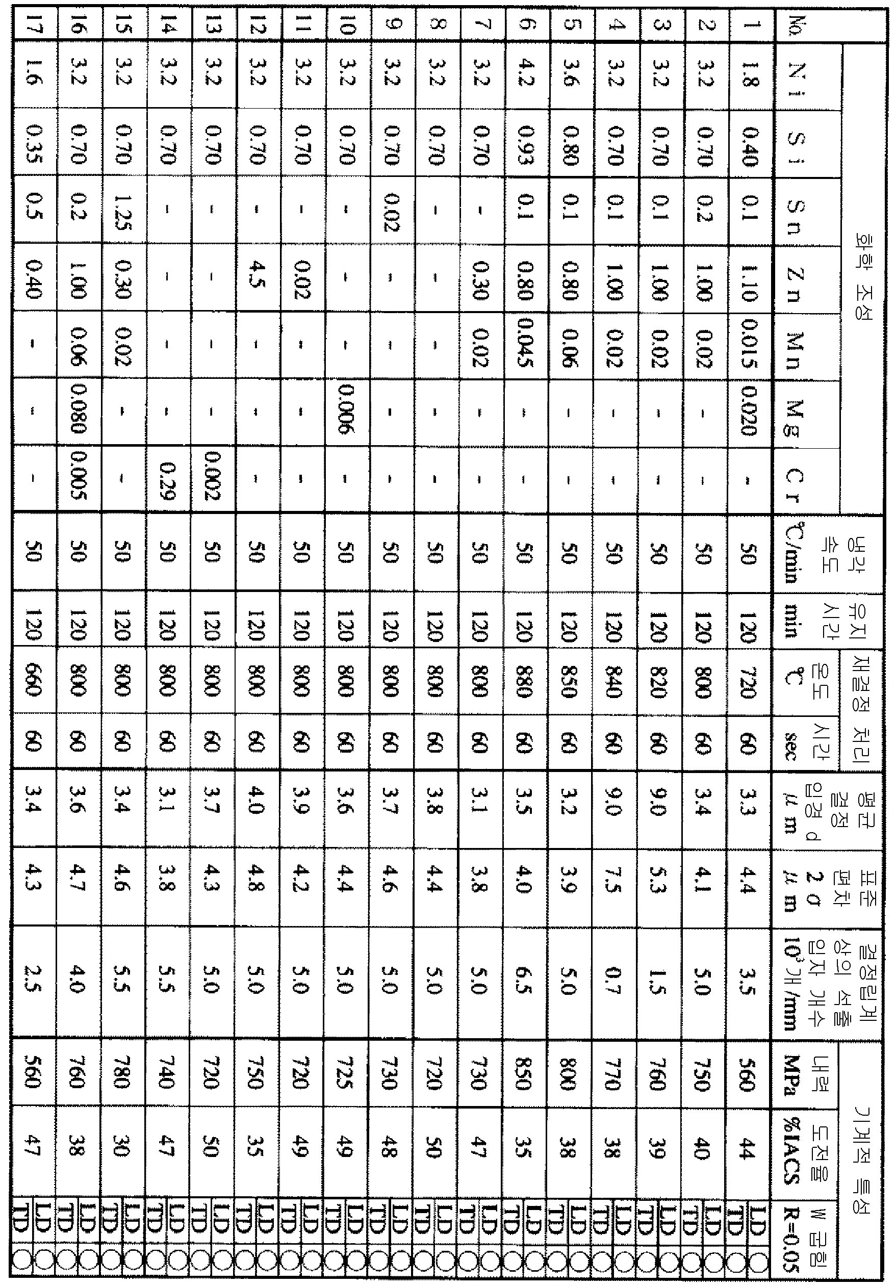
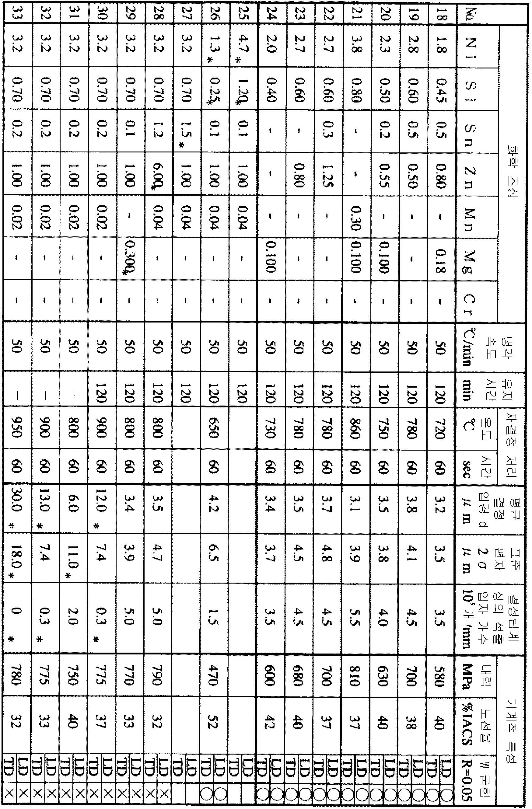
다음으로, 판의 양면을 1mm씩 면삭(面削)한 후, 두께 0.25mm까지 냉간 압연(가공률 98.6%)하고, 표 1, 2에 나타내는 조건에서 용체화를 수반하는 재결정 처리를 행하고, 이어서 수냉하였다. 단, No. 25는 Ni, Si 함유량이 과잉, No. 27은 Sn 함유량이 과잉이어서, 열간 압연에서 균열이 생겼기 때문에, 이 냉간 압연을 포함하여 이후의 공정은 수행하지 않았다.Next, after both surfaces of the plate are faced by 1 mm, they are cold rolled to a thickness of 0.25 mm (processing rate of 98.6%), and recrystallization treatment with solution is performed under the conditions shown in Tables 1 and 2, and then Water-cooled. However, No. 25 is excessive Ni, Si content, and No. Since 27 had excessive Sn content and cracked in hot rolling, subsequent processes including this cold rolling were not performed.
계속해서, 두께 0.2mm까지 냉간 압연(가공률 20%)한 후, 500℃×2시간의 석출 처리를 행하였다.Subsequently, after cold rolling (processing rate 20%) to thickness 0.2mm, the precipitation process of 500 degreeC x 2 hours was performed.
No. 1?24, 26, 28?33에 대하여, 얻어진 구리 합금판으로부터 잘라낸 시험편을 이용하고, 인장 시험에 의한 강도(0.2% 내력) 측정, 도전율 측정, W 굽힘 시험, 결정 입경의 측정, 및 결정립계 상의 분산 입자의 측정을 하기 요령으로 행하였다. 그 결과를 표 1, 2에 나타낸다.No. Using the test piece cut out from the obtained copper alloy plate about 1-24, 26, 28-33, the intensity | strength (0.2% proof strength) measurement by a tension test, electrical conductivity measurement, W bending test, the measurement of a crystal grain size, and a grain boundary phase The measurement of the dispersed particles was carried out in the following manner. The results are shown in Tables 1 and 2.
(인장 시험)(Tension test)
압연 방향을 긴 방향으로 한 JIS 5호 시험편을 이용하여, JISZ2241의 규정에 준거하여 인장 시험을 행하여 0.2% 내력을 구하였다. 내력은 500MPa 이상을 합격으로 한다.Using the JIS No. 5 test piece which made the rolling direction the long direction, the tensile test was done based on the specification of JISZ2241, and 0.2% yield strength was calculated | required. A proof strength makes 500 MPa or more pass.
(도전율 측정)(Measurement of conductivity)
압연 방향을 긴 방향으로 한 폭 10mm×길이 300mm의 시험편을 이용하여, JISH0505에 나타내진 비철 금속 재료 도전율 측정법에 준거하여, 더블 브리지(double bridge)식 전기저항 측정 장치에 의해 전기저항을 측정하고, 평균 단면적법(average cross section method)에 의해 도전율을 산출하였다.Using the test piece of width 10mm x length 300mm which made the rolling direction the longitudinal direction, based on the nonferrous metal material conductivity measuring method shown to JISH0505, electrical resistance is measured by the double bridge type electrical resistance measuring apparatus, The conductivity was calculated by the average cross section method.
(W 굽힘 시험)(W bending test)
JCBA T307에 나타내진 W 굽힘 시험에 준거하여, 압연 방향에 대하여 평행(longitudinal to rolling direction, 이하 생략하여 L.D.) 및 압연 방향에 대하여 수직(transverse to rolling direction, 이하 생략하여 T.D.)의 각 방향을 긴 방향으로 하는 폭 10mm×길이 30mm의 시험편을 이용하여, 굽힘 반경 R=0.05mm로 하여 W 굽힘 시험을 행하였다. W 굽힘 시험 후, 50배의 배율로 광학 현미경으로 굽힘 외측을 외관 관찰하여, 균열의 유무를 판정하였다. 균열 없는 경우는 ○(합격), 균열 있는 경우는 ×(불합격)로 하였다.Based on the W bending test shown in JCBA T307, each direction in parallel with the rolling direction (longitudinal to rolling direction (hereinafter abbreviated LD)) and transverse to rolling direction (hereinafter abbreviated TD) is long. W bending test was done by setting the bending radius R = 0.05mm using the test piece of width 10mm x length 30mm made into the direction. After the W bend test, the outer side of the bend was observed with an optical microscope at a magnification of 50 times to determine the presence or absence of cracks. (1) When there was no crack, it was set as X (failure) when there was a crack.
(결정 입경의 측정)(Measurement of crystal grain size)
TSL사제 후방 산란 전자 회절상 시스템(back scatter electron diffraction pattern system)을 탑재한 전계방출형 주사 전자 현미경(field-emission electron microscope)을 이용하여 결정 방위 해석법(crystal orientation analytic method)에 의해 측정하였다. 측정 영역 125×125㎛에 대하여 0.4㎛ 스텝으로 전자선을 조사하여, 결정 방위차가 15° 이상을 결정립계라고 간주하였다. 측정 영역 내의 각 결정립의 면적을 측정하고, 결정 입경(원 상당 직경)을 구하였다. 측정된 결정립의 수를 n, 각 결정립의 면적을 an, 각 결정 입경을 dn, 전체 면적을 A로 했을 때, 각 결정립의 전체 면적에 대한 점유율을 Fn(=an/A)으로 하면, 평균 결정 입경은 Σ(dn?Fn)으로 표시된다. 결정 입경 dn과 결정립의 전체 면적에 대한 점유율 Fn으로부터 결정 입경의 표준 편차 σ를 구하였다.It was measured by a crystal orientation analytic method using a field-emission electron microscope equipped with a back scatter electron diffraction pattern system manufactured by TSL. The electron beam was irradiated in 0.4 micrometer step with respect to the measurement area 125x125 micrometers, and it considered that the crystal orientation difference was 15 degree or more as a grain boundary. The area of each crystal grain in the measurement region was measured, and the crystal grain size (circle equivalent diameter) was obtained. When the number of measured grains is n, the area of each grain is an, each grain size is dn, and the total area is A, the share of the total area of each grain is Fn (= an / A). The particle diameter is represented by Σ (dn? Fn). The standard deviation σ of the grain size was determined from the grain size dn and the occupancy rate Fn of the total area of the grains.
(결정립계 상의 분산 입자의 측정)(Measurement of Dispersed Particles on Grain Boundaries)
전해 연마에 의해 박막 샘플을 작성하고, 전계방출형 전자 현미경을 이용하여 배율 50000배로 얻어진 명시야(明視野) 상(像)을 이용하여, 입계 상에 존재하는 30?300nm의 입자의 개수를 측정하였다.A thin film sample was prepared by electropolishing, and the number of particles of 30 to 300 nm present in the grain boundary was measured using a bright field image obtained at a magnification of 50000x using a field emission electron microscope. It was.
표 1, 2에 나타내는 바와 같이, No. 1?24는 본 발명에서 규정하는 조성을 갖고, 평균 결정 입경이 10㎛ 이하, 및 결정 입경의 표준 편차 σ가 2σ<10㎛라는 본 발명의 요건도 만족시킨다. 또한, 결정립계 상에 존재하는 입경 30?300nm의 분산 입자의 존재량은 어느 것이나 500개/mm 이상으로 되어 있다. 특히 No. 1, 2, 5?24는 분산 입자의 존재량이 많고, 평균 결정 입경이 5㎛ 이하로 작으며, 또한 d≤2σ를 만족시킨다. 그 특성을 보면, No. 1?24는 어느 것이나 강도 및 W 굽힘 가공성(L.D.와 T.D.의 쌍방)이 우수하다.As shown in Tables 1 and 2, No. 1-24 has the composition prescribed | regulated by this invention, and also satisfy | fills the requirements of this invention that an average crystal grain diameter is 10 micrometers or less, and the standard deviation (sigma) of a crystal grain diameter is 2 (sigma) <10 micrometers. In addition, any amount of dispersed particles having a particle size of 30 to 300 nm present on the grain boundary is 500 pieces / mm or more. Especially No. 1, 2, and 5 to 24 have a large amount of dispersed particles, a small average grain size of 5 µm or less, and satisfy d≤2σ. In view of its characteristics, Both 1 and 24 are excellent in strength and W bendability (both L.D. and T.D.).
한편, No. 26, 28, 29는 평균 결정 입경과 결정 입경의 표준 편차, 및 결정립계 상에 존재하는 입경 30?300nm의 분산 입자의 존재량이 본 발명의 규정을 만족시키지만, No. 26은 Ni 및 Si 함유량이 적기 때문에 강도가 뒤떨어지고, No. 28은 Zn 함유량이 과잉, No. 29는 Mg 함유량이 과잉이기 때문에 각각 굽힘 가공성이 뒤떨어진다.On the other hand, 26, 28, and 29 are standard deviations between the average grain size and the grain size, and the amount of dispersed particles having a particle size of 30 to 300 nm present on the grain boundaries satisfies the provisions of the present invention. 26 is inferior in strength because of its low content of Ni and Si; 28, Zn content is excessive and No. 29 is inferior to bending workability because Mg content is excessive.
No. 30은 평균 결정 입경이 규정을 초과하고, 또한 입계 상의 분산 입자의 수가 적어, 굽힘 가공성이 뒤떨어진다. Ni, Si 함유량에 비해서 재결정 처리 온도가 높아, 석출 입자가 재고용하고 입계 상의 분산 입자가 부족하여, 재결정 처리에 있어서 결정립이 조대화된 것으로 생각된다.No. The average crystal grain size of 30 exceeds the specified value, the number of dispersed particles on the grain boundary is small, and the bending workability is inferior. It is considered that the recrystallization temperature is higher than the Ni and Si content, the precipitated particles are reclaimed, the dispersed particles are insufficient in the grain boundary, and the grains are coarsened in the recrystallization treatment.
No. 31은 결정 입경의 표준 편차가 규정을 초과하여, 굽힘 가공성이 뒤떨어진다. 최종 제품에 있어서 분산 입자의 조건이 만족시켜져 있더라도 재결정 처리에 있어서 결정 입경의 표준 편차가 커진 것은, 열간 압연 후의 석출 처리를 행하지 않은 것이 영향을 준 것으로 생각된다.No. 31, the standard deviation of the crystal grain size exceeds the specification, and the bending workability is inferior. Even if the conditions of the dispersed particles are satisfied in the final product, the increase in the standard deviation of the crystal grain size in the recrystallization treatment is considered to have influenced the non-precipitation treatment after hot rolling.
No. 32는 평균 결정 입경이 규정을 초과하고, 또한 입계 상의 분산 입자의 수가 적어, 굽힘 가공성이 뒤떨어진다. 열간 압연 후의 석출 처리가 행해지지 않고, 더욱이 Ni, Si 함유량에 비해서 재결정 처리 온도가 높기 때문에 용체화가 진행하고, 입계 상의 분산 입자가 부족하여, 재결정 처리에 있어서 결정립이 조대화된 것으로 생각된다.No. The average crystal grain size of 32 exceeds the prescribed value, the number of dispersed particles on the grain boundary is small, and the bending workability is inferior. Precipitation treatment after hot rolling is not performed. Furthermore, since recrystallization temperature is higher than Ni and Si content, solution formation advances, dispersion particle | grains in a grain boundary are lacking, and it is thought that a crystal grain coarsened in recrystallization processing.
No. 33은 평균 결정 입경과 결정 입경의 표준 편차가 규정을 초과하고, 또한 입계 상에 소정 입경의 분산 입자의 수가 없어, 굽힘 가공성이 뒤떨어진다. 열간 압연 후의 석출 처리가 행해지지 않고, 더욱이 Ni, Si 함유량에 비해서 재결정 처리 온도가 높아 용체화가 진행하고, 입계 상에 핀고정 입자가 존재하지 않게 되어, 재결정 처리에 있어서 결정립이 조대화되고 또한 입경의 표준 편차가 커진 것으로 생각된다.No. The standard deviation between the average grain size and the grain size exceeds 33, and the number of dispersed particles having a predetermined grain size on the grain boundary is inferior to bending workability. Precipitation treatment after hot rolling is not performed, and further, recrystallization temperature is higher than Ni and Si content, so that solution formation proceeds and pinned particles do not exist on grain boundaries, and grains are coarsened in recrystallization treatment. It is considered that the standard deviation of the particle size is increased.
Claims (1)
Applications Claiming Priority (2)
| Application Number | Priority Date | Filing Date | Title |
|---|---|---|---|
| JP2007035726A JP4357536B2 (en) | 2007-02-16 | 2007-02-16 | Copper alloy sheet for electrical and electronic parts with excellent strength and formability |
| JPJP-P-2007-035726 | 2007-02-16 |
Related Parent Applications (1)
| Application Number | Title | Priority Date | Filing Date |
|---|---|---|---|
| KR1020097016823A Division KR101159404B1 (en) | 2007-02-16 | 2008-02-14 | Copper alloy sheet for electrical and electronic parts excelling in strength and formability |
Publications (1)
| Publication Number | Publication Date |
|---|---|
| KR20120043773A true KR20120043773A (en) | 2012-05-04 |
Family
ID=39690119
Family Applications (2)
| Application Number | Title | Priority Date | Filing Date |
|---|---|---|---|
| KR1020127008954A KR20120043773A (en) | 2007-02-16 | 2008-02-14 | Copper alloy sheet for electrical and electronic parts excelling in strength and formability |
| KR1020097016823A KR101159404B1 (en) | 2007-02-16 | 2008-02-14 | Copper alloy sheet for electrical and electronic parts excelling in strength and formability |
Family Applications After (1)
| Application Number | Title | Priority Date | Filing Date |
|---|---|---|---|
| KR1020097016823A KR101159404B1 (en) | 2007-02-16 | 2008-02-14 | Copper alloy sheet for electrical and electronic parts excelling in strength and formability |
Country Status (6)
| Country | Link |
|---|---|
| US (1) | US8784580B2 (en) |
| EP (1) | EP2128282B1 (en) |
| JP (1) | JP4357536B2 (en) |
| KR (2) | KR20120043773A (en) |
| CN (1) | CN101605917B (en) |
| WO (1) | WO2008099892A1 (en) |
Families Citing this family (60)
| Publication number | Priority date | Publication date | Assignee | Title |
|---|---|---|---|---|
| DE60324711D1 (en) * | 2003-03-03 | 2008-12-24 | Mitsubishi Shindo Kk | |
| WO2006028189A1 (en) | 2004-09-10 | 2006-03-16 | Kabushiki Kaisha Kobe Seiko Sho | Conductive material for connecting part and method for manufacturing the conductive material |
| JP5170881B2 (en) * | 2007-03-26 | 2013-03-27 | 古河電気工業株式会社 | Copper alloy material for electrical and electronic equipment and method for producing the same |
| WO2009081664A1 (en) * | 2007-12-21 | 2009-07-02 | Mitsubishi Shindoh Co., Ltd. | High-strength highly heat-conductive copper alloy pipe and process for producing the same |
| JP5394250B2 (en) | 2008-02-26 | 2014-01-22 | 三菱伸銅株式会社 | High-strength, high-conductivity copper rod |
| JP5051927B2 (en) | 2008-03-28 | 2012-10-17 | 三菱伸銅株式会社 | High-strength, high-conductivity copper alloy tube, rod, wire |
| JP4653240B2 (en) * | 2008-03-31 | 2011-03-16 | 古河電気工業株式会社 | Copper alloy materials and electrical / electronic parts for electrical / electronic equipment |
| EP2267173A4 (en) * | 2008-03-31 | 2013-09-25 | Furukawa Electric Co Ltd | Copper alloy material for electric and electronic apparatuses, and electric and electronic components |
| CN102165080B (en) | 2009-01-09 | 2013-08-21 | 三菱伸铜株式会社 | High-strength high-conductivity copper alloy rolled sheet and method for producing same |
| WO2010079708A1 (en) | 2009-01-09 | 2010-07-15 | 三菱伸銅株式会社 | High-strength high-conductivity copper alloy rolled sheet and method for producing same |
| JP2011021225A (en) * | 2009-07-15 | 2011-02-03 | Hitachi Cable Ltd | Copper alloy material for terminal/connector and method for producing the same |
| JP5400877B2 (en) * | 2009-12-02 | 2014-01-29 | 古河電気工業株式会社 | Copper alloy sheet and manufacturing method thereof |
| JP5690169B2 (en) * | 2011-02-25 | 2015-03-25 | 株式会社神戸製鋼所 | Copper alloy |
| US9845521B2 (en) * | 2010-12-13 | 2017-12-19 | Kobe Steel, Ltd. | Copper alloy |
| JP2012144789A (en) * | 2011-01-13 | 2012-08-02 | Jx Nippon Mining & Metals Corp | Cu-Co-Si-Zr ALLOY MATERIAL |
| JP5522692B2 (en) | 2011-02-16 | 2014-06-18 | 株式会社日本製鋼所 | High strength copper alloy forging |
| KR20140025607A (en) * | 2011-08-04 | 2014-03-04 | 가부시키가이샤 고베 세이코쇼 | Copper alloy |
| AU2012309363B2 (en) * | 2011-09-16 | 2015-05-28 | Mitsubishi Materials Corporation | Copper alloy sheet and production method for copper alloy sheet |
| CN103748244B (en) | 2011-09-16 | 2015-04-22 | 三菱伸铜株式会社 | Copper alloy sheet and production method for copper alloy sheet |
| JP6246454B2 (en) * | 2011-11-02 | 2017-12-13 | Jx金属株式会社 | Cu-Ni-Si alloy and method for producing the same |
| CN102418004A (en) * | 2011-11-24 | 2012-04-18 | 中铝洛阳铜业有限公司 | Nickel-chromium-silicon-bronze alloy material |
| JP6029296B2 (en) * | 2012-03-08 | 2016-11-24 | Jx金属株式会社 | Cu-Zn-Sn-Ca alloy for electrical and electronic equipment |
| JP5773929B2 (en) | 2012-03-28 | 2015-09-02 | 株式会社神戸製鋼所 | Copper alloy sheet for electrical and electronic parts with excellent bending workability and stress relaxation resistance |
| JP6154997B2 (en) * | 2012-07-13 | 2017-06-28 | 古河電気工業株式会社 | Copper alloy material excellent in strength and plating property and method for producing the same |
| JP6154996B2 (en) * | 2012-07-13 | 2017-06-28 | 古河電気工業株式会社 | High-strength copper alloy material and manufacturing method thereof |
| JP5988745B2 (en) * | 2012-07-18 | 2016-09-07 | 三菱伸銅株式会社 | Cu-Ni-Si based copper alloy plate with Sn plating and method for producing the same |
| WO2014016934A1 (en) | 2012-07-26 | 2014-01-30 | 三菱電機株式会社 | Copper alloy and production method thereof |
| CN102925746B (en) * | 2012-11-29 | 2014-09-17 | 宁波兴业鑫泰新型电子材料有限公司 | High-performance Cu-Ni-Si system copper alloy, and preparation method and processing method thereof |
| CN103146950A (en) * | 2013-01-11 | 2013-06-12 | 中南大学 | CuNiSi series elastic copper alloy and preparation method thereof |
| WO2014115307A1 (en) * | 2013-01-25 | 2014-07-31 | 三菱伸銅株式会社 | Copper-alloy plate for terminal/connector material, and method for producing copper-alloy plate for terminal/connector material |
| DE102013005158A1 (en) * | 2013-03-26 | 2014-10-02 | Kme Germany Gmbh & Co. Kg | copper alloy |
| JP6210887B2 (en) * | 2014-01-18 | 2017-10-11 | 株式会社神戸製鋼所 | Fe-P copper alloy sheet with excellent strength, heat resistance and bending workability |
| JP6173943B2 (en) * | 2014-02-20 | 2017-08-02 | 株式会社神戸製鋼所 | Copper alloy strip with surface coating layer with excellent heat resistance |
| CN106795643B (en) * | 2014-08-25 | 2019-03-05 | 株式会社神户制钢所 | The excellent connecting component conductive material of resistance to micro- skimming wear |
| CN104152742B (en) * | 2014-09-04 | 2016-04-20 | 安徽鑫科新材料股份有限公司 | A kind of high-performance tin-phosphor bronze line and production method thereof |
| CN104451250A (en) * | 2014-11-14 | 2015-03-25 | 无锡阳工机械制造有限公司 | Preparation method of brine-corrosion resistant alloy |
| CN104480346A (en) * | 2014-12-25 | 2015-04-01 | 春焱电子科技(苏州)有限公司 | Tantalum contained copper alloy for electronic material |
| CN104630556B (en) * | 2015-02-06 | 2016-08-17 | 中南大学 | High anti-corrosion CuNiSiNbSn series elastic copper alloy of a kind of ultra-high-strength/tenacity and preparation method thereof |
| JP6821290B2 (en) * | 2015-03-19 | 2021-01-27 | Jx金属株式会社 | Cu-Ni-Co-Si alloy for electronic components |
| CN104745860A (en) * | 2015-04-10 | 2015-07-01 | 苏州靖羽新材料有限公司 | Copper alloy for electronic and electrical equipment |
| CN108076645A (en) * | 2015-07-17 | 2018-05-25 | 霍尼韦尔国际公司 | The heat treatment method of metal and metal alloy articles |
| CN105420534A (en) * | 2015-11-06 | 2016-03-23 | 广西南宁智翠科技咨询有限公司 | Alloy conducting wire with ultrahigh electric conductivity |
| CN105349819B (en) * | 2015-11-26 | 2017-11-28 | 山西春雷铜材有限责任公司 | A kind of preparation method of copper alloy with high strength and high conductivity strip |
| KR101627696B1 (en) | 2015-12-28 | 2016-06-07 | 주식회사 풍산 | Copper alloy material for car and electrical and electronic components and process for producing same |
| CN105695797A (en) * | 2016-04-20 | 2016-06-22 | 苏州市相城区明达复合材料厂 | Bronze alloy for casting parts |
| CN106191725B (en) * | 2016-06-24 | 2018-01-26 | 河南江河机械有限责任公司 | High-intensity high-conductivity copper alloy nanometer phase precipitation technique method |
| CN106636736A (en) * | 2016-12-19 | 2017-05-10 | 昆山哈利法塔金属有限公司 | Copper alloy material |
| DE102017001846A1 (en) | 2017-02-25 | 2018-08-30 | Wieland-Werke Ag | Sliding element made of a copper alloy |
| CN107267806A (en) * | 2017-06-06 | 2017-10-20 | 深圳天珑无线科技有限公司 | Shell fragment and preparation method thereof, electronic installation |
| CN107586992A (en) * | 2017-09-07 | 2018-01-16 | 苏州浩焱精密模具有限公司 | A kind of copper alloy die material and preparation method thereof |
| CN108411150B (en) * | 2018-01-22 | 2019-04-05 | 公牛集团股份有限公司 | Sleeve high-performance copper alloy material and manufacturing method |
| CN108285988B (en) * | 2018-01-31 | 2019-10-18 | 宁波博威合金材料股份有限公司 | Precipitation strength type copper alloy and its application |
| CN110205515B (en) * | 2019-04-15 | 2020-07-10 | 南阳裕泰隆粉体材料有限公司 | Preparation method of corrosion-resistant Cu-Ni alloy |
| CN110860855A (en) * | 2019-10-30 | 2020-03-06 | 富威科技(吴江)有限公司 | High-surface short-flow copper strip production process |
| CN111636011A (en) * | 2020-04-26 | 2020-09-08 | 宁夏中色新材料有限公司 | High-strength high-conductivity copper-nickel-silicon alloy with good formability and preparation method thereof |
| KR102210703B1 (en) * | 2020-06-18 | 2021-02-02 | 주식회사 풍산 | Method for manufacturing copper alloy sheet for automobile or electrical and electronic parts with excellent strength and bending workability and copper alloy sheet manufactured therefrom |
| CN112877565B (en) * | 2021-01-12 | 2022-05-20 | 鞍钢股份有限公司 | Copper-steel solid-liquid bimetal composite material and preparation method thereof |
| CN113249613B (en) * | 2021-07-12 | 2021-12-14 | 江西萨瑞微电子技术有限公司 | Conductor lead for protection circuit and protection circuit comprising same |
| CN115961173A (en) * | 2021-10-08 | 2023-04-14 | 刘耀武 | Connector material, manufacturing process and connector |
| CN115652136B (en) * | 2022-10-31 | 2023-12-15 | 宁波金田铜业(集团)股份有限公司 | Free-cutting copper-nickel-silicon bar and preparation method thereof |
Family Cites Families (21)
| Publication number | Priority date | Publication date | Assignee | Title |
|---|---|---|---|---|
| JPH03162553A (en) * | 1989-11-22 | 1991-07-12 | Nippon Mining Co Ltd | Manufacture of high strength and high conductivity copper alloy having good bendability |
| JPH03188247A (en) | 1989-12-14 | 1991-08-16 | Nippon Mining Co Ltd | Production of high strength and high conductivity copper alloy excellent in bendability |
| JP2597773B2 (en) | 1991-08-30 | 1997-04-09 | 株式会社神戸製鋼所 | Method for producing high-strength copper alloy with low anisotropy |
| JP3049137B2 (en) | 1991-12-27 | 2000-06-05 | 株式会社神戸製鋼所 | High strength copper alloy excellent in bending workability and method for producing the same |
| JP3162553B2 (en) | 1993-09-13 | 2001-05-08 | 本田技研工業株式会社 | Air-fuel ratio feedback control device for internal combustion engine |
| JPH10110228A (en) | 1996-08-14 | 1998-04-28 | Furukawa Electric Co Ltd:The | Copper alloy for electronic equipment and its production |
| JP3739214B2 (en) * | 1998-03-26 | 2006-01-25 | 株式会社神戸製鋼所 | Copper alloy sheet for electronic parts |
| JP2000080428A (en) | 1998-08-31 | 2000-03-21 | Kobe Steel Ltd | Copper alloy sheet excellent in bendability |
| JP3188247B2 (en) | 1999-04-16 | 2001-07-16 | 株式会社 武田吾慎商店 | Single pipe hoop scaffold and its temporary construction method |
| JP3797882B2 (en) | 2001-03-09 | 2006-07-19 | 株式会社神戸製鋼所 | Copper alloy sheet with excellent bending workability |
| US7182823B2 (en) | 2002-07-05 | 2007-02-27 | Olin Corporation | Copper alloy containing cobalt, nickel and silicon |
| JP4166197B2 (en) | 2004-06-30 | 2008-10-15 | 日鉱金属株式会社 | Cu-Ni-Si-based copper alloy strips with excellent BadWay bending workability |
| WO2006028189A1 (en) | 2004-09-10 | 2006-03-16 | Kabushiki Kaisha Kobe Seiko Sho | Conductive material for connecting part and method for manufacturing the conductive material |
| JP4566020B2 (en) | 2005-02-14 | 2010-10-20 | 株式会社神戸製鋼所 | Copper alloy sheet for electrical and electronic parts with low anisotropy |
| CN101166840B (en) * | 2005-02-28 | 2012-07-18 | 古河电气工业株式会社 | Copper alloy |
| US20090116996A1 (en) | 2005-06-08 | 2009-05-07 | Kabushiki Kaisha Kobe Seiko Sho (Kobe Steel Ltd.) | Copper alloy, copper alloy plate, and process for producing the same |
| US20070270781A1 (en) | 2006-01-06 | 2007-11-22 | Robert Burgermeister | Medical delivery system and method for delivery of a medically useful payload |
| US8268098B2 (en) | 2006-05-26 | 2012-09-18 | Kobe Steel, Ltd. | Copper alloy having high strength, high electric conductivity and excellent bending workability |
| JP5025387B2 (en) | 2007-08-24 | 2012-09-12 | 株式会社神戸製鋼所 | Conductive material for connecting parts and method for manufacturing the same |
| FR3043069B1 (en) | 2015-10-28 | 2017-12-22 | Georges Sireix | PACKAGING |
| KR20170080320A (en) | 2015-12-31 | 2017-07-10 | 엘지디스플레이 주식회사 | Thin film transistor, display with the same, and method of fabricating the same |
-
2007
- 2007-02-16 JP JP2007035726A patent/JP4357536B2/en not_active Expired - Fee Related
-
2008
- 2008-02-14 EP EP08711294A patent/EP2128282B1/en not_active Not-in-force
- 2008-02-14 WO PCT/JP2008/052455 patent/WO2008099892A1/en active Application Filing
- 2008-02-14 KR KR1020127008954A patent/KR20120043773A/en not_active Application Discontinuation
- 2008-02-14 US US12/523,070 patent/US8784580B2/en not_active Expired - Fee Related
- 2008-02-14 CN CN2008800047301A patent/CN101605917B/en not_active Expired - Fee Related
- 2008-02-14 KR KR1020097016823A patent/KR101159404B1/en active IP Right Grant
Also Published As
| Publication number | Publication date |
|---|---|
| WO2008099892A1 (en) | 2008-08-21 |
| KR20090102849A (en) | 2009-09-30 |
| JP2008196042A (en) | 2008-08-28 |
| EP2128282A1 (en) | 2009-12-02 |
| JP4357536B2 (en) | 2009-11-04 |
| US20100047112A1 (en) | 2010-02-25 |
| EP2128282B1 (en) | 2012-08-29 |
| CN101605917A (en) | 2009-12-16 |
| EP2128282A4 (en) | 2011-06-29 |
| CN101605917B (en) | 2011-10-05 |
| KR101159404B1 (en) | 2012-06-28 |
| US8784580B2 (en) | 2014-07-22 |
Similar Documents
| Publication | Publication Date | Title |
|---|---|---|
| KR101159404B1 (en) | Copper alloy sheet for electrical and electronic parts excelling in strength and formability | |
| US8992702B2 (en) | Copper alloy sheet, manufacturing method of copper alloy sheet, and electric/electronic component | |
| KR101419147B1 (en) | Copper alloy sheet and process for producing same | |
| EP2371976B1 (en) | Cu-ni-si-co based copper ally for electronic materials and manufacturing method therefor | |
| EP2957646B1 (en) | High-strength cu-ni-co-si base copper alloy sheet, process for producing same, and current-carrying component | |
| TWI381398B (en) | Cu-Ni-Si alloy for electronic materials | |
| EP3040430B1 (en) | Copper alloy sheet material and method for producing same, and current-carrying component | |
| JP4913902B2 (en) | Method for producing copper alloy material for electric / electronic parts | |
| JP5773929B2 (en) | Copper alloy sheet for electrical and electronic parts with excellent bending workability and stress relaxation resistance | |
| KR101297485B1 (en) | Cu-ni-si-co-cr alloy for electronic material | |
| US20130056116A1 (en) | Copper alloy for electronic device, method of producing copper alloy for electronic device, and copper alloy rolled material for electronic device | |
| US9005521B2 (en) | Cu—Ni—Si alloy for electronic material | |
| WO2010126046A1 (en) | Cu-Ni-Si-Mg-BASED ALLOY HAVING IMPROVED ELECTRICAL CONDUCTIVITY AND BENDABILITY | |
| JP5657311B2 (en) | Copper alloy sheet and manufacturing method thereof | |
| KR20140056003A (en) | Cu-ni-co-si based copper alloy sheet materal and method for producing the same | |
| JP2011117034A (en) | Copper-alloy material | |
| KR20090094458A (en) | Cu-ni-si-co-base copper alloy for electronic material and process for producing the copper alloy | |
| EP2940166B1 (en) | Copper alloy for electrical and electronic equipment, copper alloy thin sheet for electrical and electronic equipment, and conductive part and terminal for electrical and electronic equipment | |
| KR102421870B1 (en) | Cu-Ni-Si-Mn-Sn based Copper alloy material with excellent strength, electrical conductivity and bendability, and method for preparing the same | |
| JP4664584B2 (en) | High strength copper alloy plate and method for producing high strength copper alloy plate | |
| JP2006037237A (en) | High strength/high conductivity copper alloy sheet and production method therefor | |
| JPH10265873A (en) | Copper alloy for electrical/electronic parts and its production | |
| KR20230030578A (en) | Copper alloys, plastically processed copper alloys, parts for electronic and electrical devices, terminals, bus bars, lead frames, and heat dissipation boards | |
| TW201714185A (en) | Cu-Co-Ni-Si Alloy for Electronic Components | |
| TWI411693B (en) | Cu-Ni-Si alloy for electronic materials |
Legal Events
| Date | Code | Title | Description |
|---|---|---|---|
| A107 | Divisional application of patent | ||
| A201 | Request for examination | ||
| E902 | Notification of reason for refusal | ||
| E601 | Decision to refuse application | ||
| J201 | Request for trial against refusal decision | ||
| J301 | Trial decision |
Free format text: TRIAL DECISION FOR APPEAL AGAINST DECISION TO DECLINE REFUSAL REQUESTED 20130123 Effective date: 20140129 |