KR20120006936A - Soft program of a non-volatile memory block - Google Patents
Soft program of a non-volatile memory block Download PDFInfo
- Publication number
- KR20120006936A KR20120006936A KR1020110068760A KR20110068760A KR20120006936A KR 20120006936 A KR20120006936 A KR 20120006936A KR 1020110068760 A KR1020110068760 A KR 1020110068760A KR 20110068760 A KR20110068760 A KR 20110068760A KR 20120006936 A KR20120006936 A KR 20120006936A
- Authority
- KR
- South Korea
- Prior art keywords
- bits
- threshold voltage
- voltage
- erased
- subset
- Prior art date
Links
Images


Classifications
-
- G—PHYSICS
- G11—INFORMATION STORAGE
- G11C—STATIC STORES
- G11C16/00—Erasable programmable read-only memories
- G11C16/02—Erasable programmable read-only memories electrically programmable
- G11C16/06—Auxiliary circuits, e.g. for writing into memory
- G11C16/34—Determination of programming status, e.g. threshold voltage, overprogramming or underprogramming, retention
- G11C16/3436—Arrangements for verifying correct programming or erasure
- G11C16/3468—Prevention of overerasure or overprogramming, e.g. by verifying whilst erasing or writing
-
- G—PHYSICS
- G11—INFORMATION STORAGE
- G11C—STATIC STORES
- G11C16/00—Erasable programmable read-only memories
- G11C16/02—Erasable programmable read-only memories electrically programmable
- G11C16/06—Auxiliary circuits, e.g. for writing into memory
- G11C16/34—Determination of programming status, e.g. threshold voltage, overprogramming or underprogramming, retention
-
- G—PHYSICS
- G11—INFORMATION STORAGE
- G11C—STATIC STORES
- G11C16/00—Erasable programmable read-only memories
- G11C16/02—Erasable programmable read-only memories electrically programmable
- G11C16/04—Erasable programmable read-only memories electrically programmable using variable threshold transistors, e.g. FAMOS
- G11C16/0483—Erasable programmable read-only memories electrically programmable using variable threshold transistors, e.g. FAMOS comprising cells having several storage transistors connected in series
-
- G—PHYSICS
- G11—INFORMATION STORAGE
- G11C—STATIC STORES
- G11C16/00—Erasable programmable read-only memories
- G11C16/02—Erasable programmable read-only memories electrically programmable
- G11C16/06—Auxiliary circuits, e.g. for writing into memory
- G11C16/10—Programming or data input circuits
- G11C16/14—Circuits for erasing electrically, e.g. erase voltage switching circuits
- G11C16/16—Circuits for erasing electrically, e.g. erase voltage switching circuits for erasing blocks, e.g. arrays, words, groups
Abstract
Description
본 출원은 일반적으로 비휘발성 메모리들에 관한 것으로서, 특히, 비휘발성 메모리 블록(non-volatile memory block)의 소프트 프로그래밍(soft programming)에 관한 것이다.The present application relates generally to nonvolatile memories, and more particularly to soft programming of non-volatile memory blocks.
비휘발성 메모리 블록(예를 들어, 플래시 또는 EEPROM)의 전형적인 소거 동작 중에, 프리-프로그램(pre-program)이 실행되어 메모리 블록의 비트들의 문턱 전압(threshold voltage)들을 프로그램 검증 전압의 레벨 또는 그 이상의 레벨로 상승시킨다. 소거 동작의 경우, 프리-프로그램 후에 Fowler-Nordheim(FN) 소거가 행해져서 메모리 블록의 비트들의 문턱 전압들을 소거 검증 전압 또는 그 이하로 낮춘다. 그러나, FN 소거 동안, 그 결과에 따른 분포는 과도하게 소거되었던 비트 셀들을 포함하고, 이로 인해 결과적으로 컬럼 누설(column leakage)이 증가하게 된다. 더욱이, 이 컬럼 누설의 문제는 비트셀들이 더욱 스케일링(scaling)됨에 따라 증가함으로써, 예를 들어 후의 프로그램 동작이 낮아진 드레인 바이어스로 인해 작동하지 않게 되거나, 또는 과소거(over-erase)된 비트들이 감지 증폭기들로 하여금 소거 및 프로그래밍된 비트를 구별하지 못하도록 할 수 있기 때문에 판독 동작이 작동하지 않게 된다. 그러므로, 컬럼 누설을 감소시키기 위해 소거된 셀들의 분포를 소프트 프로그램하거나 압축할 필요가 있다. 더욱이, 비트셀들이 더 작아지면, 총 소거 시간은 소프트 프로그램에 의해 조절된다.During a typical erase operation of a nonvolatile memory block (eg, flash or EEPROM), a pre-program is executed to set threshold voltages of bits in the memory block at or above the program verify voltage level. Raise to level. In the case of an erase operation, a Fowler-Nordheim (FN) erase is performed after the pre-program to lower the threshold voltages of the bits of the memory block to or below the erase verify voltage. However, during FN erase, the resulting distribution includes bit cells that have been over erased, resulting in increased column leakage. Moreover, the problem of column leakage increases as bitcells are more scaled, such that subsequent program operations become inoperable due to lower drain bias, or over-erased bits are detected. The read operation will not work because the amplifiers can be indistinguishable between the erased and programmed bits. Therefore, there is a need to soft program or compress the distribution of erased cells to reduce column leakage. Moreover, as bitcells become smaller, the total erase time is adjusted by the soft program.
본 발명의 목적은 컬럼 누설을 감소시키기 위해 소거된 셀들의 분포를 소프트 프로그램하거나 압축하는 것이다.It is an object of the present invention to soft program or compress the distribution of erased cells to reduce column leakage.
본 발명은 메모리 블록 내의 비트들을 소거하는 단계; 과소거된(over-erased) 비트들을 식별하는 단계; 과소거된 상기 비트들의 제 1 서브세트를 소프트 프로그래밍(soft programming)하는 단계; 상기 비트들의 제 1 서브세트를 소프트 프로그래밍한 결과들을 측정하는 단계; 상기 비트들의 제 1 서브세트를 소프트 프로그래밍한 결과들에 기초하여 복수의 가능한 전압 상태들로부터 초기 전압 상태를 선택하는 단계; 및 상기 초기 전압 상태를 비트들의 제 2 서브세트 내의 비트들에 적용하는 동안 과소거된 비트들의 제 2 서브세트를 소프트 프로그래밍하는 단계로서, 상기 제 2 서브세트는 상기 선택하는 단계가 발생할 때 여전히 과소거되어 있는 비트들을 포함하는, 상기 제 2 서브세트 소프트 프로그래밍 단계를 포함하는, 방법을 제안한다. The present invention comprises the steps of erasing bits in a memory block; Identifying over-erased bits; Soft programming a first subset of the erased bits; Measuring results of soft programming the first subset of bits; Selecting an initial voltage state from a plurality of possible voltage states based on results of soft programming the first subset of bits; And soft programming a second subset of erased bits while applying the initial voltage state to the bits in the second subset of bits, wherein the second subset is still underestimated when the selecting occurs. And a second subset soft programming step comprising the missing bits.
또한, 본 발명은 제 1의 복수의 메모리 셀들이 제 1 문턱 전압 및 제 1 문턱 전압보다 작은 제 2 문턱 전압 사이의 문턱 전압을 갖도록 소거되고, 제 2의 복수의 메모리 셀들이 제 2 문턱 전압 및 제 2 문턱 전압보다 작은 제 3 문턱 전압 사이의 문턱 전압을 갖도록 소거되고, 제 3의 복수의 메모리 셀들이 상기 제 3 문턱 전압보다 작은 문턱 전압을 갖는, 메모리 셀들의 블록을 소거하는 단계; 소프트 프로그래밍에 대한 상기 제 2의 복수의 메모리 셀들의 부분의 응답을 결정하는 단계; 상기 소프트 프로그래밍에 대한 상기 제 2의 복수의 메모리 셀들의 부분의 응답에 기초하여 소프트 프로그래밍 상태를 선택하는 단계; 및 선택 단계에서 선택되었던 프로그래밍 상태를 여전히 상기 제 2 문턱 전압 및 상기 제 3 문턱 전압 사이에서 문턱 전압을 가지는 상기 제 2 서브세트 내의 메모리 셀에, 그리고 상기 제 3의 복수의 메모리 셀에 적용하는 단계를 포함하는, 방법을 제안한다.In addition, the present invention is erased such that the first plurality of memory cells have a threshold voltage between the first threshold voltage and the second threshold voltage less than the first threshold voltage, and the second plurality of memory cells are separated from the second threshold voltage and the second threshold voltage. Erasing the block of memory cells erased to have a threshold voltage between a third threshold voltage less than a second threshold voltage, and wherein the third plurality of memory cells have a threshold voltage less than the third threshold voltage; Determining a response of the portion of the second plurality of memory cells to soft programming; Selecting a soft programming state based on a response of the portion of the second plurality of memory cells to the soft programming; And applying a programming state that was selected in the selecting step to a memory cell in the second subset that still has a threshold voltage between the second threshold voltage and the third threshold voltage, and to the third plurality of memory cells. Proposing a method, including.
또한, 본 발명은 메모리 블록 내의 모든 비트들을 소거하는 단계; 상기 소거하는 단계에 의해 상기 메모리 블록 내의 어떤 비트들이 과소거되었는지를 식별하는 단계; 소프트 프로그래밍 동안 인가되는 바람직한 게이트 전압을 결정하기 위해 상기 소거하는 단계에 의해 과소거된 메모리 블록 내의 비트들의 부분을 테스트하는 단계로서, 바람직한 게이트 전압에서 소프트 프로그래밍하여 테스트되는 비트들의 적어도 미리 결정된 퍼센티지의 문턱 전압을, 가장 낮은 바람직한 문턱 전압 및 최대의 바람직한 문턱 전압 사이의 적어도 중간 문턱 전압으로 증가하도록 하는, 상기 테스트 단계; 및 나머지 과소거된 비트들 모두를 소프트 프로그래밍하기 위하여 상기 비트들의 게이트들에 인가되는 바람직한 게이트 전압을 이용하는 단계를 포함하는, 방법을 제안한다.The present invention also provides a method of erasing all bits in a memory block; Identifying which bits in the memory block have been erased by the erasing step; Testing a portion of bits in a memory block that are erased by said erasing to determine a desired gate voltage applied during soft programming, said threshold of at least a predetermined percentage of bits tested by soft programming at the desired gate voltage. The testing step of causing the voltage to increase to at least an intermediate threshold voltage between the lowest desired threshold voltage and the maximum desired threshold voltage; And using the desired gate voltage applied to the gates of the bits to soft program all of the remaining erased bits.
도 1은 하나의 실시예에 따른 집적 회로를 블록도 형태로 도시한 도면.
도 2는 하나의 실시예에 따른 도 1의 플래시 메모리의 일부를 부분 개략도 및 부분 블록도 형태로 도시한 도면.
도 3은 플래시 메모리의 블록 내의 비트셀들의 예시적인 비트 분포들을 그래픽 형태로 도시한 도면.
도 4는 하나의 실시예에 따른 소거 동작을 흐름도 형태로 도시한 도면.
도 5는 하나의 실시예에 따라, 후속 소프트 프로그래밍에 대한 초기 전압을결정하기 위한 프로세스를 흐름도 형태로 도시한 도면.1 is a block diagram of an integrated circuit in accordance with one embodiment;
2 illustrates, in partial schematic and partial block diagram form, a portion of the flash memory of FIG. 1 in accordance with one embodiment;
3 is a graphical illustration of example bit distributions of bitcells in a block of flash memory;
4 is a flowchart illustrating an erase operation according to an exemplary embodiment.
FIG. 5 illustrates, in flow diagram form, a process for determining an initial voltage for subsequent soft programming, in accordance with an embodiment.
본 발명은 예를 통해 설명되지만 첨부 도면들에 의해 제한되지 않고, 첨부 도면들에서 동일한 참조번호들은 유사한 요소들을 표시한다. 도면들에서의 요소들은 간소화 및 명료하게 도시되므로 반드시 축적대로 도시되지 않는다.The invention is illustrated by way of example but not limitation by the accompanying drawings, in which like reference numerals designate like elements. Elements in the figures are simplified and clearly shown and are not necessarily drawn to scale.
하나의 실시예에서, 비휘발성 메모리 블록의 소거 동작은 메모리 블록을 프리프로그래밍하는 단계, 메모리 블록을 FN 소거하는 단계, 후속 소프트 프로그래밍을 위한 초기 전압을 결정하기 위해 적응성 프로세스를 이용하는 단계, 및 그 후에 메모리 블록 내의 소거된 비트들의 분포를 압축하기 위해 결정된 초기 전압을 이용하여 메모리 블록을 소프트 프로그래밍하는 단계를 포함한다. 메모리 블록들의 소거 동안, 메모리 블록 내의 비트들은 과소거될 수 있다. 비트는 자체의 문턱 전압이 소거된 비트에 대하여 허용 가능한 최소 문턱 전압 이하일 때 과소거된 것으로 간주될 수 있다. 그러므로, 메모리 블록의 소프트 프로그래밍 동안, 컬럼 누설을 감소하는데 일조하는 허용 가능한 레벨로 비트들의 문턱 전압들을 증가시키기 위해 과도하게 소거되었던 비트들에 프로그래밍 펄스들이 반복해서 적용된다. 하나의 실시예에서, 적응성 프로세스 동안 결정되는 초기 전압은 소프트 프로그래밍 동안 프로그래밍 펄스로서 초기에 인가되는 게이트 전압이다. 이 실시예에서, 적응성 프로세스는 메모리 블록 내의 비트들의 서브세트를 이용하여 초기 게이트 전압을 결정하며, 결과적으로 후속하는 소프트 프로그래밍에 대한 반복들이, 더욱 보존성인(conservative) 게이트 전압으로 시작하는 현재의 방법들과 비교해서, 더욱 감소한다. 대안으로, 적응성 프로세스는 소프트 프로그래밍 동안 이용될 초기 게이트 전압(예를 들어 드레인 전압과 같은) 외에 또는 대신에, 다른 초기 전압을 또는 상태들을 결정하는데 이용될 수 있다. 그러므로, 시간을 내어 적응성 프로세스를 실행하여 소프트 프로그래밍에 대한 개선된 초기 전압을 결정함으로써, 후속 소프트 프로그래밍 동안 반복들의 횟수(및 그에 따른 시간)이 감소할 수 있다.In one embodiment, the erase operation of the nonvolatile memory block comprises preprogramming the memory block, FN erasing the memory block, using an adaptive process to determine an initial voltage for subsequent soft programming, and thereafter. Soft programming the memory block using the determined initial voltage to compress the distribution of erased bits in the memory block. During erase of the memory blocks, the bits in the memory block may be overwritten. A bit can be considered over-erased when its threshold voltage is below the minimum allowable threshold voltage for the erased bit. Therefore, during soft programming of the memory block, programming pulses are repeatedly applied to bits that have been excessively erased to increase the threshold voltages of the bits to an acceptable level, which helps to reduce column leakage. In one embodiment, the initial voltage determined during the adaptive process is the gate voltage initially applied as a programming pulse during soft programming. In this embodiment, the adaptive process uses the subset of bits in the memory block to determine the initial gate voltage, with the result that current iterations for subsequent soft programming begin with a more conservative gate voltage. In comparison with these. Alternatively, the adaptive process can be used to determine other initial voltages or states in addition to or instead of the initial gate voltage (such as, for example, the drain voltage) to be used during soft programming. Therefore, by taking the time to execute the adaptive process to determine the improved initial voltage for soft programming, the number of iterations (and thus time) during subsequent soft programming can be reduced.
도 1은 하나의 실시예에 따른 집적 회로(10)를 블록도 형태로 도시한다. 도시된 실시예에서, 집적 회로(IC)(10)는 하나 이상의 프로세서들(12), 하나 이상의 플래시 메모리들(14), 하나 이상의 다른 메모리들(16), 하나 이상의 다른 모듈들(18), 및 버스(22)를 통해 양방향으로 결합될 수 있는 외부 버스 인터페이스(20)를 포함한다. 대안의 실시예들은 프로세서(12)를 가지지 않을 수 있고, 다른 메모리(16)를 가지지 않을 수 있고, 다른 모듈들(18)을 가지지 않을 수 있고, 그리고/또는 외부 버스 인터페이스(20)를 가지지 않을 수 있다. 도시된 실시예에서, 외부 버스 인터페이스(20)는 정보를 IC(10)로 그리고 IC(10)로부터 통신하는데 이용될 수 있는 외부 버스(24)에 결합된다. 하나의 실시예에서, 모듈들(12, 14, 16 및 18) 중 하나 이상은 IC(10)의 외부에 있는 하나 이상의 집적 회로 단자들(도시되지 않음)을 가질 수 있다. 일부 실시예들에서, IC(10)는 하나 이상의 플래시 메모리들(14)만을 가질 수 있음을 주목하라.1 illustrates, in block diagram form, an
도 2는 일 실시예에 따른 플래시 메모리(14)의 일부를 부분 개략도 및 부분 블록도 형태로 도시한다. 플래시 메모리(14)는 메모리 셀들(예를 들어 비트셀들)의 메모리 어레이(memory array)(103)를 포함한다. 도시된 실시예에서, 메모리 어레이(103)는 네 비트셀들(105, 107, 109, 및 111)을 포함한다. 하나의 실시예에서, 다른 유형들의 플래시 메모리 셀들(예를 들어, 나노크리스탈(nanocrystal)들, 스플릿 게이트 플래시(split gate flash), 질화물계 메모리들)이 구현될 수 있을지라도 셀들은 부동 게이트 플래시 메모리 셀(floating gate flash memory cell)들이다. 또한 다른 유형들의 비트셀들(예를 들어, EEPROM 셀들)이 어레이(103)에서 구현될 수 있다. 어레이(103)는 메모리(14)의 하나의 메모리 블록을 나타내고, 여기서 메모리(14)는 임의의 수효의 메모리 블록들을 포함할 수 있다. 메모리 블록의 소거 중에, 메모리 블록의 각각의 비트셀은 대량으로 소거된다. 예를 들어, 어레이(103)의 소거 동안, 비트셀들(105, 107, 109, 및 111)의 각각은 대량으로 소거된다. 도시된 실시예에서, 어레이(103)는 설명을 위해 4개의 메모리 셀들(2개의 로우(row)들 및 2개의 컬럼들을 포함한다)을 포함하지만, 다른 실시예들에서 더 많은 수의 로우들 및 컬럼들을 포함할 수 있다. 예를 들어, 어레이(103)의 각각의 로우는 약 4096 비트들을 포함할 수 있고, 여기서 각각의 로우는 페이지(page)들로 추가로 세그먼트될 수 있다. 하나의 실시예에서, 하나의 페이지는 256비트들을 포함하고 페이지의 모든 비트는 고정된 수의 비트들로 분리된다. 예를 들어, 각각의 로우가 16 페이지들로 세그먼트되면, 로우의 매 16번째 비트는 동일한 페이지에 속한다.2 illustrates a portion of a
메모리(14)는 메모리 동작들 중에 게이트 전압들(Vw)을 워드 라인(word line) 전압 제어 회로(117)로부터 워드 라인들(WL0 및 WL1)로 선택적으로 제공하기 위한 로우 디코더(row decoder)(115)를 포함한다. 이 워드 라인들은 어레이(103)의 메모리 셀들의 게이트들에 접속된다. 메모리(14)는 또한 메모리 동작들 중에 어레이(103)의 셀들을 판독하기 위하여 비트 라인들(BL0 및 BL1)에 결합하는 감지 증폭기들 및 Vdrain 전압을 드레인 전압 제어 회로(125)로부터 비트 라인들(BL0 및 BL1)로 인가하기 위한 회로 소자를 포함하는 컬럼 디코더 및 감지 증폭기 회로(121)를 포함한다. 메모리(14)는 또한 비트셀들의 소스들에 공통 소스 전압을 인가하는 소스 제어기(127)를 포함한다. 회로(121)는 데이터 라인들 상의 셀들로부터 판독되는 데이터를 출력한다. 메모리(14)는 또한 셀들의 전압 판독들을 위해 회로(121)의 기준 감지 증폭기에 기준 전류(Iref)를 공급하는 전류 기준 회로(123)를 포함한다.The
메모리(14)는 동작 중에 메모리(14)의 동작들을 제어하기 위한 메모리 제어기(113)를 포함한다. 제어기(113)는 워드라인 전압 제어기(117), 기준 회로(123), 드레인 전압 제어기(125), 및 소스 제어기(127)를 제어하여 메모리 동작 동안 상기 회로들에 의해 제공되는 전압 및 전류 값들을 제어한다. 메모리 제어기(113)는 또한 제어 정보를 제공하여 메모리 동작 동안 로우 디코드 회로(115) 및 회로(121)의 동작들을 제어한다. 제어기(113)는 메모리 동작들을 실행하기 위해, 외부 소스(예를 들어, 프로세서(12))로부터 어드레스, 데이터, 및 제어 정보를 수신하는 어드레스, 데이터, 및 제어 라인들을 포함한다. 제어기(113)는 또한 하나 이상의 카운터(counter)들(138) 및 저장 회로소자(130)를 포함한다. 저장 회로소자(130)는 예를 들어 목표 전압(target voltage(TV): 130), 드레인 전압, 및/또는 게이트 전압(후술되는 바와 같이, 소프트 프로그래밍동안 이용될 수 있다)을 저장할 수 있다. 예를 들어, 저장 회로소자(130)는 TV를 저장하기 위한 레지스터(register)(132), 드레인 전압을 저장하기 위한 레지스터(134), 및/또는 게이트 전압을 저장하기 위한 레지스터(136)를 포함할 수 있다. 후술되는 바와 같이, TV는 초기 게이트 전압 및/또는 어레이(103)의 소프트 프로그래밍 동안 이용될 드레인 전압을 결정하는데 이용될 수 있다. 다른 메모리 회로들은 다른 실시예들에서 다른 구성들을 가질 수 있음을 주목하라. 메모리(14)의 동작은 소거 동작에 관해서처럼, 도 3 내지 도 5를 참조하여 더 자세하게 후술될 것이다. 로우 디코더(115) 및 컬럼 디코더 및 감지 증폭기(121)는 당업계에 공지되어 있는 바와 같이 동작할 수 있음을 주목하라.The
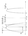
도 3은 하나의 실시예에 따른 소거된 비트셀들 및 프로그래밍된 비트셀들에 대한 비트셀 문턱 전압 분포들을 그래픽 형태로 도시한다. 수직 축은 로그 스케일을 이용한다. 도시된 그래프에서, 곡선(202)은 플래시 메모리(14)의 메모리 블록 내의 비트셀들이 소거 동작 중에 그러나 소프트 프로그래밍 전에 소거될 때 특정 문턱 전압(수평 축에 의해 표시된다)을 갖는 비트셀들의 수(수직 축에 의해 표시된다)를 도시한다. 도시된 그래프에서, 곡선(204)은 플래시 메모리(14)의 메모리 블록 내의 비트셀들이 소거 동작 동안 그리고 소프트 프로그래밍 후에 소거될 때 특정 문턱 전압(수평 축에 의해 표시된다)을 갖는 비트셀들의 수(수직 축에 의해 표시된다)를 도시한다. 소프트 프로그래밍은 소거된 비트들 분포를 압축하여 분포 중 가장 많이 소거된 측(분포의 최좌측의 부분)이 화살표(200)에 의해 도시되는 바와 같이, 소프트 프로그램 검증 전압(soft program verify voltage: SPV)에 의해 표현되는 최소 허용 가능 문턱 전압까지 이동하게 된다.(SPV는 또한 소거된 메모리 셀에 대한 가장 낮은 바람직한 문턱 전압으로 칭해질 수 있음을 주목하라) 예를 들어, 자신의 문턱 전압이 SPV 또는 그 이하인 상기 소거된 비트들은 과소거된 것으로 간주될 수 있다. 그러므로, 소프트 프로그래밍 동안, 모든 소거된 비트들이 적어도 SPV의 문턱 전압을 가지도록 분포를 압축하기 위해서 단지 상기 과소거된 비트들만이 소프트 프로그래밍된다. 이 방식에서, 곡선(202)의 분포와 비교해서, 감소한 컬럼 누설이 달성된다. 도시된 그래프에서, 모든 소거된 비트들은 기껏해야 소거 검증 전압(EV)의 문턱 전압을 갖는다.(EV는 또한 소거된 메모리 셀에 대한 최대의 바람직한 문턱 전압으로 칭해질 수 있다.) 또한, 하나의 실시예에서, 분포의 최대 소거 측만이 화살표(200)에 의해 도시되는 바와 같이, 소프트 프로그래밍 동안 시프트되고, 반면에, 분포의 최소 소거 측(분포의 가장 우측의 부분)은 시프트되지 않고 EV 또는 그 이하에서 유지된다.3 illustrates, in graphical form, bitcell threshold voltage distributions for erased bitcells and programmed bitcells, according to one embodiment. The vertical axis uses log scale. In the graph shown, curve 202 shows the number of bitcells having a certain threshold voltage (indicated by the horizontal axis) when the bitcells in the memory block of
또한 도시된 그래프에서, 곡선(206)은 플래시 메모리(14)의 메모리 블록 내의 비트 셀들이 프로그래밍될 때 특정 전압(수평 축에 의해 표시된다)을 갖는 비트 셀들의 수(수직 축에 의해 표시된다)를 도시한다. 도시된 그래프에서, 모든 프로그래밍된 비트들은 프로그램 검증 전압(PV) 또는 그 이상의 문턱 전압을 갖는다. 도 3에서 판독 전압 및 EV 사이의 수평 갭은 비트셀들의 판독된 하나의 마진(margin)의 양을 나타내고, 반면에 도 3에서 판독 전압 및 PV 사이의 수평 갭은 비트셀들의 판독된 영 마진의 양의 나타낸다.Also in the graph shown,
하나의 실시예에서, 목표 전압(TV)은 SPV 및 EV 사이에 있도록 선택되고, 후술되는 바와 같이, 소프트 프로그래밍을 위한 초기 게이트 전압을 결정하는데 이용될 것이다. 하나의 실시예에서, TV는 SPV 및 EV 사이의 중간에 있다. 또한, 하나의 실시예에서, 저 전압(LV)은 최대로 소거된 비트(most erased bit : MEB)의 문턱 전압 및 SPV 사이에서 선택되고, 이는 또한, 후술되는 바와 같이, 소프트 프로그래밍을 위한 초기 게이트 전압을 결정하는데 이용될 수 있다.In one embodiment, the target voltage TV is chosen to be between SPV and EV and will be used to determine the initial gate voltage for soft programming, as described below. In one embodiment, the TV is in between the SPV and the EV. Further, in one embodiment, the low voltage LV is selected between the threshold voltage and SPV of the most erased bit (MEB), which is also an initial gate for soft programming, as described below. It can be used to determine the voltage.
도 4는 본 발명의 실시예에 따른 소거 동작(250)을 흐름도 형태로 도시한다. 소거 동작(250)는 메모리(14)의 블록 단위로(per block basis) 기초하여 실행된다. 예를 들어, 소거 동작(250)은 어레이(103) 전부에 대해 실행될 수 있다. 소거 동작은 메모리(14)의 블록이 프리-프로그래밍되는 단계 252로 시작한다. 하나의 실시예에서, 프리-프로그래밍하는 동안, 각각의 비트셀은 PV를 이용하여 검증되고, 비트셀의 문턱 전압이 PV 이하인 경우, 프로그램 펄스가 인가된다. 그 후에, 각각의 비트셀은 PV를 이용하여 다시 검증되고, 비트셀의 문턱 전압이 여전히 PV 이하라면, 후속 프로그램 펄스가 인가된다. 블록을 미리 프로그램한 후에, 프로그래밍된 비트 분포는 도 3의 곡선(206)에 의해 도시되는 바와 같이, PV 또는 그 이상이어야만 한다.4 illustrates, in flow chart form, an erase
그리고나서 플로우는 단계 254로 진행하고 여기서 프리-프로그래밍되었던 메모리(14)의 블록이 FN 소거된다. 하나의 실시예에서, 이 FN 소거 동안, 각각의 비트셀은 EV를 이용하여 검증되고, 비트셀의 문턱 전압이 EV 이상인 경우, FN 소거 펄스가 인가된다. 그후에, 각각의 비트셀이 EV를 이용하여 다시 검증되고, 비트셀의 문턱 전압이 여전히 EV 이상이면, 후속 펄스가 인가된다. FN 소거 펄스를 인가하는 각각의 반복 동안, 더 강한 FN 소거 펄스가 인가될 수 있다. 블록을 FN 소거한 후에, 소거된 비트 분포는 도 3에서 곡선(202)에 의해 도시된 바와 같이, EV 또는 그 이하여야만 하는데, 왜냐하면 EV는 소거되기 위한 최대의 바람직한 문턱 전압이기 때문이다.The flow then proceeds to step 254 where the block of
그리고나서 플로우는 단계 256으로 진행하고 여기서 적응성 프로세스가 실행되어 블록의 후속 소프트 프로그래밍에서 이용하기 위한 초기 게이트 전압이 결정된다. 이 초기 게이트 전압을 결정하기 위한 프로세스는 도 5를 참조하여 더욱 상세하게 기술될 것이다.The flow then proceeds to step 256 where an adaptive process is executed to determine the initial gate voltage for use in subsequent soft programming of the block. The process for determining this initial gate voltage will be described in more detail with reference to FIG.
그리고나서 플로우는 단계 258 및 단계 260으로 진행하고 여기서 블록은 소프트 프로그래밍된다. 예를 들어, 단계 256 후에, 플로우는 단계 258로 진행하고, 여기서 단계 256에서의 적응성 프로세스에 의해 결정된 초기 게이트 전압은 블록의 소프트 프로그래밍 동안 인가된다. 예를 들어, SPV에서 검증되지 않은 블록 내의 각각의 비트셀의 경우(이미 SPV 또는 그 이상에 있지 않다), 단계 256에서 초기 소프트 프로그래밍 펄스는 결정된 초기 게이트 전압으로 인가된다. 그리고나서 플로우는 단계 260으로 진행하고 여기서 블록 내의 모든 비트들이 SPV 또는 그 이상이 될 때까지 게이트 전압을 반복해서 증가하는데 왜냐하면 SPV는 소거되기 위한 최소의 바람직한 문턱 전압이기 때문이다. 예를 들어, 초기 소프트 프로그래밍 펄스가 SPV에서 검증되지 않은 과소거된 비트셀들에 인가된 후에, 다른 검증이 실행되어 어느 비트셀들이 SPV에서 아직 검증되지 않은지가(즉, 여전히 과소거되어 있는지)가 결정된다. 이 비트셀들의 경우, 증가된 게이트 전압이 인가된다. 증가하고 있는 게이트 전압의 검증 및 인가는 블록 내의 모든 비트들이 SPV 또는 그 이상이 될 때까지 교대로 실행된다. 이 지점에서, 소거 동작이 완료된다. 하나의 실시예에서, 소거 동작(250)은 이용자 모드 임베디드 소거 동작(user mode embedded erase operation)으로 칭해진다.The flow then proceeds to step 258 and step 260 where the block is soft programmed. For example, after
도 5는 하나의 실시예에 따른 도 4의 단계 256의 적응식 프로세스의 더욱 상세한 버전을 흐름도 형식으로 도시한다. 도 4의 단계 254로부터, 플로우는 도 5의 단계 270으로 진행하고 여기서 초기 보존성 게이트 전압은 소프트 프로그래밍에 인가될 현재의 게이트 전압으로 선택되고 소거 동작이 실행되고 있는 블록의 초기 테스트 페이지는 현재의 테스트 페이지로 선택된다. 보존성 게이트 전압은, 예를 들어 과소거된 비트들이 과 소프트 프로그래밍되지 않는(즉, EV보다 높은 레벨로 프로그래밍되지 않는) 것을 보장하도록 선택된다. 그리고나서 플로우는 단계 272로 진행하고, 현재의 테스트 페이지 내에서 미리 결정된 양만큼 과소거된 비트들을 결정하기 위해 하나 이상의 판독들이 실행된다.(단계 272를 통한 제 1 시간에서 테스트 페이지는 단계 270에서 선택된 초기 테스트 페이지로 칭해짐을 주의하라.) 예를 들어, 하나의 실시예에서, 어느 비트들이 SPV 또는 그 이하인지 결정하기 위해 현재의 테스트 페이지의 제 1 검증 판독이 SPV에서 실행될 수 있고, 어느 비트들이 LV 또는 그 이상인지 결정하기 위해 현재의 테스트 페이지의 제 2 검증 판독이 LV에서 실행될 수 있다. 이 정보에 있어서, 문턱 접압들이 LV 및 SPV 사이에 해당하는 비트들은, 전체를 포함하여 결정될 수 있다. 그러므로, 이 예에서, 미리 결정된 양만큼 과소거되는 비트들은 문턱 전압들이 SPV 또는 그 이하이지만 LV 또는 그 이상인 비트들이다. 다른 실시예에서, 미리 결정된 양은 상이할 수 있고, 예를 들어, LV와 같은 더 작은 문턱 전압을 이용하지 않고 과소거되는 임의의 비트(즉, 문턱 전압이 SPV 또는 그 이하인 임의의 비트)를 포함할 수 있다. 하나의 실시예에서, 현재의 테스트 페이지에서 미리 결정된 양에 의해 얼마나 많은 비트들이 과소거되는지에 대한 카운트가 결정되고 예를 들어 제어기(113)에 저장될 수 있다. 또한, 컬럼 디코더 및 감지 증폭기(121)로부터 출력된 데이터 라인들을 이용하는 카운터(138)는 과소거된 비트들의 수를 결정할 수 있다.FIG. 5 illustrates, in flow chart form, a more detailed version of the adaptive process of
그리고나서 플로우는 단계 274로 진행하고 여기서 현재의 게이트 전압은 단계 272에서 결정되었던 비트들을 소프트 프로그래밍하기 위해 펄스 인가 동안 인가된다. 예를 들어, 미리 결정된 양만큼 과소거된 것으로 결정되었던 현재의 테스트 페이지 내에서의 상기 비트들의 경우, 현재의 게이트 전압을 이용하는 소프트 프로그램 펄스가 인가된다. 단계 274를 통한 제 1 시간에서, 현재의 게이트 전압은 초기 보존성 게이트 전압이고 현재의 테스트 페이지는 초기 테스트 페이지이다.The flow then proceeds to step 274 where the current gate voltage is applied during pulse application to soft program the bits that were determined in
그리고나서 플로우는 결정 단계 276으로 진행하고 여기서 소프트 프로그래밍된 결정된 비트들(즉, 단계 274에서 소프트 프로그래밍된 상기 비트들)의 적어도 미리 결정된 퍼센티지가 미리 결정된 목표 전압(TV)에서 검증되는지가 결정된다. 하나의 실시예에서, 미리 결정된 퍼센티지는 50퍼센트이다. 그러므로, 이 예의 경우, 단계 274에서 소프트 프로그램 펄스를 수신하였던 상기 비트들의 적어도 50%가 TV 또는 그 이상의(하나의 실시예에서, 제어기(113) 내에 저장되는) 문턱 전압을 갖는지가 결정된다. 만일 그렇지 않다면, 플로우는 단계 278로 진행하고 여기서 현재의 게이트 전압을 점진적으로 증가시키고 새로운 테스트 페이지가 현재의 테스트 페이지로 선택된다. 이 새로운 페이지는 전에 이용된 테스트 페이지와 상이하다. 하나의 실시예에서, 블록 278에서 선택된 각각의 새로운 테스트 페이지는 현재의 소거 동작 중에 테스트 페이지로 선택되는 임의의 이전 페이지와는 상이하다. 또한, 하나의 실시예에서, 게이트 전압 증가는 조정 가능하다. 결정 단계 276에서, 단계 274에서 소프트 프로그램 펄스를 수신했던 상기 비트들의 적어도 50%가 TV 또는 그 이상의 문턱 전압을 가지는 경우, 플로우는 단계 280으로 진행하고 여기서 현재의 게이트 전압은 단계 258 및 260에서 실행될 후속 소프트 프로그램을 위한 초기 게이트 전압으로 이용하기 위해 저장된다(예를 들어, 레지스터(136)와 같은, 제어기(113)에). 즉, 저장된 현재의 게이트 전압은, 소프트 프로그래밍된 결정된 비트들(즉, 단계 272에서 결정되고 단계 274에서 소프트 프로그래밍된 상기 비트들)의 적어도 미리 결정된 퍼센티지의 문턱 전압을 적어도 TV로까지 증가시키므로, 후에 후속 소프트 프로그래밍을 위한 초기 게이트 전압으로 이용된다. 그리고나서 플로우는 도 4의 단계 258로 계속된다.The flow then proceeds to
그러므로, 도 5의 적응성 프로세스는 메모리 블록의 선택된 서브세트의 이용을 가능하게 하여 전체 메모리 블록의 소프트 프로그래밍을 시작할 수 있는 가장 양호한 초기 게이트 전압을 인지하고 결정한다. 이 방식에서, 후속 소프트 프로그래밍은 보존성이 더 큰 게이트 전압으로 시작하는 것과 비교하여 반복들을 더 적게 이용할 수 있다. 도 5에서 실행된 초기 게이트 전압의 결정이 완료되는데 시간을 필요로 할지라도, 소거 동작의 총 소거 시간을 지배하는 전체 블록을 소프트 프로그래밍하는 동안 요구되는 반복들의 수를 감소시킴으로써 전체 시간이 절약된다. 대안의 실시예들에서, 페이지 이외의 메모리 블록의 다른 서브세트들은 후속 소프트 프로그램을 위한 초기 게이트 전압을 결정하는데 이용될 수 있음을 주목하라. 또한, 대안의 실시예들에서, 메모리 블록의 소프트 프로그래밍을 시작할 최선의 드레인 전압을 반복해서 결정하기 위해 도 5의 프로세스와 유사한 프로세스가 이용될 수 있다. 즉, 초기 게이트 전압을 결정하기 보다는 오히려, 초기 드레인 전압이 대신 결정되어 소프트 프로그래밍하기 위한 시작 지점으로 이용될 수 있고, 여기서 드레인 전압은 단계 260에서 소프트 프로그래밍 동안 반속해서 증가한다. 또 다른 대안의 실시예에서, 도 5의 프로세스는 후속 소프트 프로그램을 위하여 초기의 게이트 전압 및 초기의 드레인 전압 이 둘 모두를 결정하기 위해 이용될 수 있다. 대안의 실시예들은 메모리 블록의 선택된 서브세트를 이용하여 다른 파라미터들 또는 초기 소프트 프로그래밍 상태들을 결정하거나 또는 후속 소프트 프로그램 동안 이용될 수 있는 다른 결과들을 측정할 수 있다. 즉, 후속 소프트 프로그램 동안 이용될 수 있는 게이트 전압 및/또는 드레인 전압은 단지, 메모리의 선택된 서브세트의 응답 또는 결과들에 기초하여 결정되거나 선택될 수 있는 초기 소프트 프로그래밍 상태들의 예들이다.Therefore, the adaptive process of FIG. 5 enables the use of a selected subset of memory blocks to recognize and determine the best initial gate voltage at which to begin soft programming of the entire memory block. In this way, subsequent soft programming can use fewer iterations as compared to starting with a higher gate voltage. Although it takes time for the determination of the initial gate voltage performed in FIG. 5 to complete, the overall time is saved by reducing the number of iterations required during soft programming of the entire block that governs the total erase time of the erase operation. Note that in alternative embodiments, other subsets of the memory block other than the page may be used to determine the initial gate voltage for subsequent soft programs. Also, in alternative embodiments, a process similar to the process of FIG. 5 may be used to repeatedly determine the best drain voltage to begin soft programming of the memory block. That is, rather than determining the initial gate voltage, the initial drain voltage may instead be determined and used as a starting point for soft programming, where the drain voltage is increased at a constant rate during soft programming in
본 발명을 구현하는 장치들이, 대부분, 당업계에 공지되어 있는 구성요소들 및 회로들로 구성되므로, 본 발명의 기본 개념들의 이해 및 인식을 위해 그리고 본 발명의 내용들을 애매하게 하거나 본 발명의 내용들을 벗어나지 않도록 하기 위해, 회로 세부사항들은 상술한 바와 같이 필요한 것으로 간주되는 범위보다 넓게 설명되지 않을 것이다.Apparatuses for implementing the present invention, for the most part, are composed of components and circuits known in the art, for the purpose of understanding and recognizing the basic concepts of the present invention and for obscuring the contents of the present invention or In order not to deviate, the circuit details will not be described broadly beyond the extent deemed necessary as described above.
본 발명이 특정 전도 유형들 또는 전위들의 극성들에 대해 설명되었을지라도, 당업자들은 전도 유형들 및 전위들의 극성들이 반전될 수 있음을 인식하였다.Although the present invention has been described with respect to the polarities of specific conduction types or potentials, those skilled in the art have recognized that the polarities of conduction types and potentials may be reversed.
더욱이, 명세서 및 청구항들에서의 용어들 "전방", "후방", "상부", "하부", "위", "아래" 등이, 만일 있다면, 설명의 목적을 위해 이용되므로 반드시 영구적인 상대 위치들을 기술하는 것은 아니다. 그렇게 이용되는 용어들은 적절한 환경들 하에서 상호 교환 가능하므로 본원에 기술되는 발명의 실시예들은 예를 들어 상기 도시되거나 또는 다른 방식으로 본원에 기술된 것과는 다른 배향(orientation)들로의 동작이 가능하다는 것이 이해된다.Moreover, the terms "front", "rear", "upper", "lower", "up", "down", and the like in the specification and claims, if any, are used only for the purpose of explanation and are therefore necessarily permanent counterparts. It does not describe the locations. It is understood that the terms so used are interchangeable under appropriate circumstances so that embodiments of the invention described herein are capable of operating in orientations other than, for example, those shown above or described herein in other ways. .
본원에서 기술되는 아키텍처들은 단지 예시이고, 실제로 동일한 기능을 성취하는 많은 다른 아키텍처들이 구현될 수 있음이 이해될 것이다. 더욱이, 당업자는 상술한 동작들의 기능 사이의 경계들이 단지 예시임을 인식할 것이다. 다수의 동작들의 기능은 단일 동작으로 결합될 수 있고, 그리고/또는 단일 동작의 기능은 추가 동작들로 분배될 수 있다. 더욱이, 대안의 실시예들은 특정 동작의 다수의 경우들을 포함할 수 있고, 동작들의 순서는 다양한 다른 실시예들에서 변경될 수 있다.It will be appreciated that the architectures described herein are merely examples and that many other architectures may be implemented that actually achieve the same functionality. Moreover, those skilled in the art will recognize that the boundaries between the functions of the above described operations are merely examples. The functions of multiple operations may be combined into a single operation, and / or the function of a single operation may be divided into additional operations. Moreover, alternative embodiments may include multiple instances of a particular operation, and the order of the operations may be changed in various other embodiments.
본 발명이 본원에서 특정한 실시예들을 참고하여 설명될지라도, 이하 청구항들에서 진술된 본 발명의 범위를 범위를 벗어나지 않고 다양한 수정들 및 변경들이 행해질 수 있다. 예를 들어, 적응성 프로세스는 소프트 프로그램을 위한 게이트 전압과는 다른, 또는 상기 게이트 전압 외의 여러 파라미터들에 대한 초기 값들을 결정하는데 이용될 수 있다. 따라서, 명세서 및 도면들은 제한의 의미라기보다는 설명의 의미로 간주되어야만 하고, 모든 그와 같은 수정들은 본 발명의 범위 내에 포함되도록 의도된다. 특정한 실시예들에 대하여 본원에 기술되는 문제점들에 대한 이점들, 장점들 및 해법들은 임의의 또는 모든 청구항들의 결정적이거나, 필수적이거나, 본질적인 특성 또는 요소로 해석되도록 의도되지 않는다.Although the invention has been described herein with reference to specific embodiments, various modifications and changes can be made without departing from the scope of the invention as set forth in the claims below. For example, an adaptive process can be used to determine initial values for various parameters other than, or other than the gate voltage for, the soft program. Accordingly, the specification and figures are to be regarded in an illustrative rather than a restrictive sense, and all such modifications are intended to be included within the scope of present invention. The advantages, advantages and solutions to the problems described herein for specific embodiments are not intended to be construed as critical, essential, or essential features or elements of any or all of the claims.
본원에서 이용되는 용어 "결합되다"는 직접적인 결합 또는 기계적 결합으로 제한되도록 의도되지 않는다.As used herein, the term “coupled” is not intended to be limited to direct bonding or mechanical bonding.
본원에서 이용되는 용어들 "a", 또는 "an"은 하나 또는 하나 이상으로 규정된다. 또한, 심지어 동일한 청구항이 도입 어구들 "하나 이상의" 또는 "적어도 하나" 및 "a" 또는 "an"과 같은 부정 관사들을 포함할 때에도, 청구항들에서 "적어도 하나" 및 "하나 이상의"와 같은 도입 어구들을 이용하는 경우, 부정 관사들 "a", 또는 "an"에 의해 다른 청구항 요소들이 도입되면, 그와 같이 도입된 청구항 요소들을 포함하는 임의의 특정한 청구항이, 발명들을 그러한 요소를 단 하나 포함하는것으로 제한하는 것을 의미하는 것으로 해석되어서는 안 된다. 정관사의 이용에 있어서도 마찬가지로 유지된다.As used herein, the terms "a" or "an" are defined as one or more than one. Also, even when the same claim includes indefinite articles such as "one or more" or "at least one" and "a" or "an", introductions such as "at least one" and "one or more" in the claims. When using the phrases, if other claim elements are introduced by the indefinite articles "a", or "an", then any particular claim, including the claim elements so introduced, includes the invention with only one such element. It should not be construed as meaning limited to. The same holds true for the use of definite articles.
달리 진술되지 않으면, "제 1" 및 "제 2"와 같은 용어들은 그와 같은 용어들이 기술하는 요소들 사이를 임의로 구분하는데 이용된다. 그러므로, 이 용어들은 반드시 그와 같은 요소들의 임시 또는 다른 우선순위를 표시하도록 의도된 것은 아니다.Unless stated otherwise, terms such as "first" and "second" are used to arbitrarily distinguish between the elements that such terms describe. Therefore, these terms are not necessarily intended to indicate a temporary or other priority of such elements.
다음은 본 발명의 다양한 실시예들이다.The following are various embodiments of the present invention.
아이템 1은 메모리 블록 내의 비트들을 소거하는 단계; 과소거된 비트들을 식별하는 단계; 과소거된 비트들의 제 1 서브세트를 소프트 프로그래밍하는 단계; 비트들의 제 1 서브세트를 소프트 프로그래밍한 결과들을 측정하는 단계; 비트들의 제 1 서브세트를 소프트 프로그래밍한 결과들에 기초하여 복수의 가능한 전압 상태들로부터 초기 전압 상태를 선택하는 단계; 및 초기 전압 상태를 비트들의 제 2 서브세트 내의 비트들에 적용하는 동안 과소거된 비트들의 제 2 서브세트를 소프트 프로그래밍하는 단계를 포함하는 방법을 포함하고, 여기서 제 2 서브세트는 선택 단계가 발생할 때 여전히 과소거되어 있는 비트들을 포함한다. 아이템 2는 아이템 1의 방법을 포함하고, 추가 소프트 프로그래밍을 필요로 하는 비트들의 제 2 서브세트 내에 비트들의 제 3 서브세트가 존재하는지를 결정하는 단계; 및 비트들의 제 3 서브세트가 존재하는 경우, 초기 전압 상태보다 높은 전압을 포함하는 비트들의 제 3 서브세트의 비트들에 인가되는 전압 상태를 이용하여 비트들의 제 3 서브세트를 소프트 프로그래밍하는 단계를 추가로 포함한다. 아이템 3은 아이템 1의 방법을 포함하고, 여기서 비트들은 게이트들을 갖고 비트들의 제 1 서브세트를 소프트 프로그래밍하는 단계는 제 1 페이지의 과소거된 비트들의 게이트들에 인가되는 초기 보존성 게이트 전압을 이용하는 단계를 포함하고, 여기서 제 1 페이지의 과소거된 비트들은 비트들의 제 1 서브세트 내에 있다. 아이템 4는 아이템 3의 방법을 포함하고, 여기서 측정하는 단계가 제 1 페이지의 과소거된 비트들이 충분히 소프트 프로그래밍되지 않는다고 결정하면, 비트들의 제 1 서브세트를 소프트 프로그래밍하는 단계는 제 2 페이지의 과소거된 비트들의 게이트들에 인가되는 제 1 증가 전압을 이용하는 단계를 추가로 포함하고, 여기서 제 2 페이지의 과소거된 비트들은 비트들의 제 1 서브세트 내에 있다. 아이템 5는 아이템 4의 방법을 포함하고, 여기서 측정하는 단계가 제 2 페이지의 과소거된 비트들이 충분히 소프트 프로그래밍되지 않는다고 결정하면, 비트들의 제 1 서브세트를 소프트 프로그래밍하는 단계는 제 3 페이지의 과소거된 비트들의 게이트들에 인가되는 제 1 증가 전압보다 큰 제 2 증가 전압을 이용하는 단계를 추가로 포함하고, 여기서 제 3 페이지의 과소거된 비트들은 비트들의 제 1 서브세트 내에 있다. 아이템 6은 아이템 5의 방법을 포함하고, 선택하는 단계는 소프트 프로그래밍 단계 동안 이용되는 게이트 전압을 초기 전압 상태로서 선택하는 단계를 포함하며, 소프트 프로그래밍 단계는 소거되기 위한 최소의 바람직한 문턱 전압 이상 소거되기 위한 최대의 바람직한 문턱 전압보다 작은 적어도 제 1 문턱 전압까지 증가되는 비트들의 적어도 미리 결정된 퍼센티지를 발생시킨다. 아이템 7은 아이템 1의 방법을 포함하고, 과소거된 비트들을 식별하는 단계는 미리결정된 양보다 적게 과소거된 비트들을 식별하는 것을 추가로 특징으로 한다. 아이템 8은 아이템 7의 방법을 포함하고, 여기서 비트들의 제 1 서브세트를 소프트 프로그래밍하는 단계는 미리 결정된 양보다 적게 과소거된 비트들만을 포함하는 것을 추가로 특징으로 하는 비트들의 제 1 서브세트를 특징으로 한다. 아이템 9는 아이템 1의 방법을 포함하고, 제 2 서브세트를 소프트 프로그래밍하는 단계에 의해 비트들 모두가 제 1 문턱 전압 및 제 1 문턱 전압보다 큰 제 2 문턱 전압 사이의 문턱 전압을 갖게 되는지를 결정하는 단계를 추가로 포함하고, 여기서 비트가 제 1 문턱 전압 이하의 문턱 전압을 갖는 경우, 비트 내에 과소거 상태가 존재한다. 아이템 10은 아이템 9의 방법을 포함하고, 비트들 모두가 제 1 문턱 전압 및 제 2 문턱 전압 사이의 문턱 전압을 가질 때까지 증가하는 전압 상태들을 이용하여 소프트 프로그래밍을 계속하는 단계를 추가로 포함한다.Item 1 includes erasing bits in the memory block; Identifying the over-erased bits; Soft programming a first subset of erased bits; Measuring results of soft programming the first subset of bits; Selecting an initial voltage state from the plurality of possible voltage states based on results of soft programming the first subset of bits; And soft programming a second subset of erased bits while applying an initial voltage state to the bits in the second subset of bits, wherein the second subset is to cause a selection step to occur. Contains bits that are still over-erased. Item 2 includes the method of item 1, and determining whether there is a third subset of bits in the second subset of bits that require additional soft programming; And if there is a third subset of bits, soft programming the third subset of bits using a voltage state applied to the bits of the third subset of bits that includes a voltage higher than the initial voltage state. Additionally included. Item 3 includes the method of item 1, wherein the bits have gates and soft programming the first subset of bits using an initial conservative gate voltage applied to the gates of the erased bits of the first page. Wherein the over-erased bits of the first page are in a first subset of bits. Item 4 includes the method of item 3, wherein if the measuring determines that the erased bits of the first page are not sufficiently soft programmed, then soft programming the first subset of bits is underestimated on the second page. Using the first increasing voltage applied to the gates of the erased bits, wherein the over-erased bits of the second page are in a first subset of bits. Item 5 includes the method of item 4, wherein if the measuring determines that the erased bits of the second page are not sufficiently soft programmed, then soft programming the first subset of bits is underestimated on the third page. Using a second increase voltage greater than a first increase voltage applied to the gates of the erased bits, wherein the over-erased bits of the third page are in a first subset of bits. Item 6 includes the method of item 5, wherein the selecting comprises selecting as an initial voltage state the gate voltage used during the soft programming step, wherein the soft programming step is erased above a minimum desired threshold voltage to be erased. Generate at least a predetermined percentage of bits that are increased to at least a first threshold voltage less than the maximum desired threshold voltage. Item 7 includes the method of item 1, and wherein identifying the over-erased bits is further characterized by identifying over-erased bits less than a predetermined amount. Item 8 includes the method of item 7, wherein the soft programming of the first subset of bits further comprises a first subset of bits, further comprising only bits that are less than a predetermined amount. It features. Item 9 includes the method of item 1, wherein soft programming the second subset determines whether all of the bits have a threshold voltage between the first threshold voltage and a second threshold voltage greater than the first threshold voltage. Further comprising the step of: wherein if the bit has a threshold voltage less than or equal to the first threshold voltage, there is an over erased state in the bit.
아이템 11은 제 1의 복수의 메모리 셀들이 제 1 문턱 전압 및 제 1 문턱 전압보다 작은 제 2 문턱 전압 사이의 문턱 전압을 갖도록 소거되고, 제 2의 복수의 메모리 셀들이 제 2 문턱 전압 및 제 2 문턱 전압보다 작은 제 3 문턱 전압 사이의 문턱 전압을 갖도록 소거되고, 제 3의 복수의 메모리 셀들이 제 3 문턱 전압보다 작은 문턱 전압을 갖는 메모리 셀들의 블록을 소거하는 단계; 소프트 프로그래밍에 대한 제 2의 복수의 메모리 셀들의 부분의 응답을 결정하는 단계; 소프트 프로그래밍에 대한 제 2의 복수의 메모리 셀들의 부분의 응답에 기초하여 소프트 프로그래밍 상태를 선택하는 단계; 및 선택 단계에서 선택되었던 프로그래밍 상태를 여전히 제 2 문턱 전압 및 제 3 문턱 전압 사이에서 문턱 전압을 가지는 제 2 서브세트 내의 메모리 셀에, 그리고 제 3의 복수의 메모리 셀에 적용하는 단계를 포함하는 방법을 포함한다. 아이템 12는 아이템 11의 방법을 포함하고, 여기서 선택되었던 프로그래밍 상태는 초기 게이트 전압이었다. 아이템 13은 아이템 11의 방법을 포함하고, 메모리 셀들 모두가 제 1 문턱 전압 및 제 2 문턱 전압 사이에 있을 때까지 소프트 프로그래밍을 실행하는 단계를 추가로 포함한다. 아이템 14는 아이템 11의 방법을 포함하고, 여기서 응답을 결정하는 단계는 제 2의 복수의 메모리 셀들의 샘플이 제 4 문턱 전압 및 제 1 문턱 전압 사이의 문턱 전압을 갖는 샘플 내의 메모리 셀들의 적어도 미리 결정된 프랙션(fraction)의 결과로 응답할 때까지 소프트 프로그래밍을 실행하는 단계를 포함하고, 여기서 제 4 문턱 전압은 제 1 문턱 전압보다 작고 제 2 문턱 전압보다 크다. 아이템 15는 아이템 14의 방법을 포함하고, 소프트 프로그래밍 상태를 선택하는 단계는 제 4 문턱 전압 및 제 1 문턱 전압 사이의 문턱 전압을 갖는 샘플들 내의 메모리 셀들의 적어도 절반을 발생시켰던 소프트 프로그래밍 동안 이용되는, 샘플들 내의 메모리 셀들의 게이트들에 인가되었던 게이트 전압을 선택하는 단계를 포함한다. 아이템 16은 아이템 15의 방법을 포함하고, 여기서 제 4 문턱 전압은 제 1 문턱 전압 및 제 2 문턱 전압의 중간이다. 아이템 17은 아이템 16의 방법을 포함하고, 여기서 미리 결정된 프랙션은 절반이다.Item 11 is erased such that the first plurality of memory cells has a threshold voltage between the first threshold voltage and the second threshold voltage less than the first threshold voltage, and the second plurality of memory cells is the second threshold voltage and the second threshold voltage. Erasing the block of memory cells erased to have a threshold voltage between the third threshold voltage less than the threshold voltage and the third plurality of memory cells having a threshold voltage less than the third threshold voltage; Determining a response of the portion of the second plurality of memory cells to soft programming; Selecting a soft programming state based on a response of the portion of the second plurality of memory cells to soft programming; And applying the programming state that was selected in the selecting step to a memory cell in the second subset that still has a threshold voltage between the second and third threshold voltages, and to the third plurality of memory cells. It includes.
아이템 18은 메모리 블록 내의 모든 비트들을 소거하는 단계; 소거 단계에 의해 메모리 블록 내의 어떤 비트들이 과소거되었는지를 식별하는 단계; 소프트 프로그래밍 동안 인가되는 바람직한 게이트 전압을 결정하기 위해 소거 단계에 의해 과소거된 메모리 블록 내의 비트들의 부분을 테스트하는 단계로서, 바람직한 게이트 전압에서 소프트 프로그래밍하여 테스트되는 비트들의 적어도 미리 결정된 퍼센티지의 문턱 전압을, 가장 낮은 바람직한 문턱 전압 및 최대의 바람직한 문턱 전압 사이의 적어도 중간 문턱 전압으로 증가하도록 하는, 상기 테스트 단계; 및 나머지 과소거된 비트들 모두를 소프트 프로그래밍하기 위하여 비트들의 게이트들에 인가되는 바람직한 게이트 전압을 이용하는 단계를 포함한다. 아이템 19는 아이템 18의 방법을 포함하고, 여기서 테스트하는 단계는 바람직한 게이트 전압이 비트들의 샘플에 도달할 때까지 비트들의 샘플들을 소프트 프로그래밍하기 위해 증가하는 게이트 전압들을 인가하는 단계를 포함한다. 아이템 20은 아이템 19의 방법을 포함하고, 여기서 소프트 프로그래밍은 적어도 최소 문턱 전압을 갖는 과소거된 비트들의 샘플들에 적용된다.
10 : 집적 회로 12 : 프로세서 14 : 플래시 메모리
20 : 외부 버스 인터페이스 10
20: external bus interface
Claims (20)
과소거된(over-erased) 비트들을 식별하는 단계;
과소거된 상기 비트들의 제 1 서브세트를 소프트 프로그래밍(soft programming)하는 단계;
상기 비트들의 제 1 서브세트를 소프트 프로그래밍한 결과들을 측정하는 단계;
상기 비트들의 제 1 서브세트를 소프트 프로그래밍한 결과들에 기초하여 복수의 가능한 전압 상태들로부터 초기 전압 상태를 선택하는 단계; 및
상기 초기 전압 상태를 비트들의 제 2 서브세트 내의 비트들에 적용하는 동안 과소거된 비트들의 제 2 서브세트를 소프트 프로그래밍하는 단계로서, 상기 제 2 서브세트는 상기 선택하는 단계가 발생할 때 여전히 과소거되어 있는 비트들을 포함하는, 상기 제 2 서브세트 소프트 프로그래밍 단계를 포함하는, 방법.Erasing bits in the memory block;
Identifying over-erased bits;
Soft programming a first subset of the erased bits;
Measuring results of soft programming the first subset of bits;
Selecting an initial voltage state from a plurality of possible voltage states based on results of soft programming the first subset of bits; And
Soft programming a second subset of over-erased bits while applying the initial voltage state to the bits in the second subset of bits, wherein the second subset is still over-erased when the selecting occurs. And a second subset soft programming step comprising bits that are reserved.
추가 소프트 프로그래밍을 필요로 하는 상기 비트들의 제 2 서브세트 내에 비트들의 제 3 서브세트가 존재하는지를 결정하는 단계; 및
비트들의 제 3 서브세트가 존재하는 경우, 상기 초기 전압 상태보다 높은 전압을 포함하는 비트들의 제 3 서브세트의 비트들에 인가되는 전압 상태를 이용하여 상기 비트들의 제 3 서브세트를 소프트 프로그래밍하는 단계를 추가로 포함하는, 방법.The method of claim 1,
Determining if there is a third subset of bits in the second subset of bits that require additional soft programming; And
If there is a third subset of bits, soft programming the third subset of bits using a voltage state applied to the bits of the third subset of bits that includes a voltage higher than the initial voltage state. Further comprising.
소프트 프로그래밍에 대한 상기 제 2의 복수의 메모리 셀들의 부분의 응답을 결정하는 단계;
상기 소프트 프로그래밍에 대한 상기 제 2의 복수의 메모리 셀들의 부분의 응답에 기초하여 소프트 프로그래밍 상태를 선택하는 단계; 및
선택 단계에서 선택되었던 프로그래밍 상태를 여전히 상기 제 2 문턱 전압 및 상기 제 3 문턱 전압 사이에서 문턱 전압을 가지는 상기 제 2 서브세트 내의 메모리 셀에, 그리고 상기 제 3의 복수의 메모리 셀에 적용하는 단계를 포함하는, 방법. The first plurality of memory cells are erased to have a threshold voltage between the first threshold voltage and the second threshold voltage less than the first threshold voltage, and the second plurality of memory cells is less than the second threshold voltage and the second threshold voltage. Erasing a block of memory cells, wherein the third plurality of memory cells have a threshold voltage less than the third threshold voltage and are erased to have a threshold voltage between the small third threshold voltage;
Determining a response of the portion of the second plurality of memory cells to soft programming;
Selecting a soft programming state based on a response of the portion of the second plurality of memory cells to the soft programming; And
Applying a programming state that was selected in the selecting step to a memory cell in the second subset that still has a threshold voltage between the second threshold voltage and the third threshold voltage, and to the third plurality of memory cells; Including, method.
상기 소거하는 단계에 의해 상기 메모리 블록 내의 어떤 비트들이 과소거되었는지를 식별하는 단계;
소프트 프로그래밍 동안 인가되는 바람직한 게이트 전압을 결정하기 위해 상기 소거하는 단계에 의해 과소거된 메모리 블록 내의 비트들의 부분을 테스트하는 단계로서, 바람직한 게이트 전압에서 소프트 프로그래밍하여 테스트되는 비트들의 적어도 미리 결정된 퍼센티지의 문턱 전압을, 가장 낮은 바람직한 문턱 전압 및 최대의 바람직한 문턱 전압 사이의 적어도 중간 문턱 전압으로 증가하도록 하는, 상기 테스트 단계; 및
나머지 과소거된 비트들 모두를 소프트 프로그래밍하기 위하여 상기 비트들의 게이트들에 인가되는 바람직한 게이트 전압을 이용하는 단계를 포함하는, 방법.Erasing all the bits in the memory block;
Identifying which bits in the memory block have been erased by the erasing step;
Testing a portion of bits in a memory block that are erased by said erasing to determine a desired gate voltage applied during soft programming, said threshold of at least a predetermined percentage of bits tested by soft programming at the desired gate voltage. The testing step of causing the voltage to increase to at least an intermediate threshold voltage between the lowest desired threshold voltage and the maximum desired threshold voltage; And
Using a desired gate voltage applied to the gates of the bits to soft program all of the remaining erased bits.
Applications Claiming Priority (2)
| Application Number | Priority Date | Filing Date | Title |
|---|---|---|---|
| US12/835,309 US8351276B2 (en) | 2010-07-13 | 2010-07-13 | Soft program of a non-volatile memory block |
| US12/835,309 | 2010-07-13 |
Publications (1)
| Publication Number | Publication Date |
|---|---|
| KR20120006936A true KR20120006936A (en) | 2012-01-19 |
Family
ID=45466890
Family Applications (1)
| Application Number | Title | Priority Date | Filing Date |
|---|---|---|---|
| KR1020110068760A KR20120006936A (en) | 2010-07-13 | 2011-07-12 | Soft program of a non-volatile memory block |
Country Status (3)
| Country | Link |
|---|---|
| US (1) | US8351276B2 (en) |
| JP (1) | JP2012022767A (en) |
| KR (1) | KR20120006936A (en) |
Cited By (2)
| Publication number | Priority date | Publication date | Assignee | Title |
|---|---|---|---|---|
| KR20190079305A (en) * | 2017-12-27 | 2019-07-05 | 삼성전자주식회사 | Method of erasing data in nonvolatile memory device and nonvolatile memory device performing the same |
| KR20200040021A (en) * | 2018-10-08 | 2020-04-17 | 에스케이하이닉스 주식회사 | Memory device and operating method thereof |
Families Citing this family (7)
| Publication number | Priority date | Publication date | Assignee | Title |
|---|---|---|---|---|
| US8391068B2 (en) * | 2010-12-20 | 2013-03-05 | Texas Instruments Incorporated | Adaptive programming for flash memories |
| US9009547B2 (en) | 2011-01-27 | 2015-04-14 | Apple Inc. | Advanced programming verification schemes for analog memory cells |
| US9129700B2 (en) * | 2013-01-22 | 2015-09-08 | Freescale Semiconductor, Inc. | Systems and methods for adaptive soft programming for non-volatile memory using temperature sensor |
| KR102309841B1 (en) | 2015-08-24 | 2021-10-12 | 삼성전자주식회사 | Data storage including recovery function for threshold voltage distribution change of memory cells according to applying surface mounting technology and operating method thereof |
| KR102491134B1 (en) * | 2018-09-21 | 2023-01-25 | 에스케이하이닉스 주식회사 | Memory system, operating method thereof and non-volatile memory device |
| KR102569820B1 (en) * | 2018-10-25 | 2023-08-24 | 에스케이하이닉스 주식회사 | Memory controller and operating method thereof |
| JP2021047961A (en) * | 2019-09-19 | 2021-03-25 | キオクシア株式会社 | Memory system |
Family Cites Families (8)
| Publication number | Priority date | Publication date | Assignee | Title |
|---|---|---|---|---|
| US6496417B1 (en) * | 1999-06-08 | 2002-12-17 | Macronix International Co., Ltd. | Method and integrated circuit for bit line soft programming (BLISP) |
| US7177199B2 (en) | 2003-10-20 | 2007-02-13 | Sandisk Corporation | Behavior based programming of non-volatile memory |
| US7092290B2 (en) | 2004-11-16 | 2006-08-15 | Sandisk Corporation | High speed programming system with reduced over programming |
| US7023737B1 (en) | 2005-08-01 | 2006-04-04 | Sandisk Corporation | System for programming non-volatile memory with self-adjusting maximum program loop |
| US7616500B2 (en) | 2007-02-20 | 2009-11-10 | Sandisk Corporation | Non-volatile storage apparatus with multiple pass write sequence |
| EP2348511B1 (en) * | 2007-02-20 | 2014-08-13 | SanDisk Technologies, Inc. | Variable program for non-volatile storage |
| KR100953045B1 (en) * | 2008-05-23 | 2010-04-14 | 주식회사 하이닉스반도체 | Programming method of non volatile memory device |
| US7839690B2 (en) * | 2008-12-11 | 2010-11-23 | Sandisk Corporation | Adaptive erase and soft programming for memory |
-
2010
- 2010-07-13 US US12/835,309 patent/US8351276B2/en not_active Expired - Fee Related
-
2011
- 2011-07-12 KR KR1020110068760A patent/KR20120006936A/en not_active Application Discontinuation
- 2011-07-12 JP JP2011153682A patent/JP2012022767A/en active Pending
Cited By (2)
| Publication number | Priority date | Publication date | Assignee | Title |
|---|---|---|---|---|
| KR20190079305A (en) * | 2017-12-27 | 2019-07-05 | 삼성전자주식회사 | Method of erasing data in nonvolatile memory device and nonvolatile memory device performing the same |
| KR20200040021A (en) * | 2018-10-08 | 2020-04-17 | 에스케이하이닉스 주식회사 | Memory device and operating method thereof |
Also Published As
| Publication number | Publication date |
|---|---|
| JP2012022767A (en) | 2012-02-02 |
| US20120014179A1 (en) | 2012-01-19 |
| US8351276B2 (en) | 2013-01-08 |
| CN102376370A (en) | 2012-03-14 |
Similar Documents
| Publication | Publication Date | Title |
|---|---|---|
| JP4360736B2 (en) | Nonvolatile semiconductor memory device and data erasing method of nonvolatile semiconductor memory device | |
| KR100890016B1 (en) | Nonvolatile memory device, memory system having its and program method thereof | |
| KR20120006936A (en) | Soft program of a non-volatile memory block | |
| KR100875538B1 (en) | Nonvolatile memory device and its program and erase method | |
| US7453731B2 (en) | Method for non-volatile memory with linear estimation of initial programming voltage | |
| US8018769B2 (en) | Non-volatile memory with linear estimation of initial programming voltage | |
| US6975538B2 (en) | Memory block erasing in a flash memory device | |
| KR101463967B1 (en) | Non-volatile semiconductor memory, erasing method and programming method | |
| JP4646534B2 (en) | Programming based on the behavior of non-volatile memory | |
| KR102098266B1 (en) | Semiconductor memory device | |
| US6515908B2 (en) | Nonvolatile semiconductor memory device having reduced erase time and method of erasing data of the same | |
| CN102422362B (en) | Multiple level program verify in a memory device | |
| JP4593159B2 (en) | Semiconductor device | |
| KR100672172B1 (en) | Programming method of flash memory device for improving program speed of the flash memory device using incremental step pulse programming | |
| US7639533B2 (en) | Multi-level memory cell programming methods | |
| US7606077B2 (en) | Non-volatile memory with reduced erase/write cycling during trimming of initial programming voltage | |
| JP2005506653A (en) | Method for erasing a memory cell | |
| US20030206435A1 (en) | Nonvolatile semiconductor storage device and data erasing method | |
| JP2007035214A (en) | Nonvolatile semiconductor storage device | |
| KR20100043935A (en) | Non-volatile memory device and program method thereof | |
| KR20090032246A (en) | Non volatile memory device and method for operating thereof | |
| JP2013125576A (en) | Nonvolatile semiconductor storage device | |
| KR20130139598A (en) | Semiconductor memory device and method of operating the same | |
| KR20120030818A (en) | Non-volatile memory device and erase method thereof | |
| JP2014044786A (en) | Non-volatile memory (nvm) that uses soft programming |
Legal Events
| Date | Code | Title | Description |
|---|---|---|---|
| WITN | Application deemed withdrawn, e.g. because no request for examination was filed or no examination fee was paid |