KR20110000695A - Method for improving pv aesthetics and efficiency - Google Patents
Method for improving pv aesthetics and efficiency Download PDFInfo
- Publication number
- KR20110000695A KR20110000695A KR1020107025055A KR20107025055A KR20110000695A KR 20110000695 A KR20110000695 A KR 20110000695A KR 1020107025055 A KR1020107025055 A KR 1020107025055A KR 20107025055 A KR20107025055 A KR 20107025055A KR 20110000695 A KR20110000695 A KR 20110000695A
- Authority
- KR
- South Korea
- Prior art keywords
- photovoltaic
- conductor
- light
- photovoltaic device
- incident
- Prior art date
Links
- 238000000034 method Methods 0.000 title claims description 34
- 239000004020 conductor Substances 0.000 claims abstract description 141
- 239000000463 material Substances 0.000 claims abstract description 80
- 230000008859 change Effects 0.000 claims abstract description 20
- 238000004519 manufacturing process Methods 0.000 claims abstract description 12
- 230000003287 optical effect Effects 0.000 claims description 18
- 230000005611 electricity Effects 0.000 claims description 14
- 230000008569 process Effects 0.000 claims description 11
- 238000010248 power generation Methods 0.000 claims description 8
- 238000009792 diffusion process Methods 0.000 claims description 5
- 238000011084 recovery Methods 0.000 claims description 5
- 238000001020 plasma etching Methods 0.000 claims description 4
- 239000003973 paint Substances 0.000 claims description 3
- 238000000059 patterning Methods 0.000 claims description 2
- 238000001093 holography Methods 0.000 claims 1
- 239000002245 particle Substances 0.000 claims 1
- 239000010410 layer Substances 0.000 description 43
- 239000011149 active material Substances 0.000 description 25
- 239000010409 thin film Substances 0.000 description 22
- 239000004065 semiconductor Substances 0.000 description 13
- 230000008901 benefit Effects 0.000 description 12
- 239000005038 ethylene vinyl acetate Substances 0.000 description 8
- 239000011521 glass Substances 0.000 description 8
- 229920001200 poly(ethylene-vinyl acetate) Polymers 0.000 description 8
- 239000000758 substrate Substances 0.000 description 8
- 239000006059 cover glass Substances 0.000 description 7
- 239000000969 carrier Substances 0.000 description 6
- 230000006872 improvement Effects 0.000 description 6
- 238000007789 sealing Methods 0.000 description 5
- 238000010521 absorption reaction Methods 0.000 description 4
- 239000002803 fossil fuel Substances 0.000 description 4
- 229910052710 silicon Inorganic materials 0.000 description 4
- 239000010703 silicon Substances 0.000 description 4
- 235000012431 wafers Nutrition 0.000 description 4
- MARUHZGHZWCEQU-UHFFFAOYSA-N 5-phenyl-2h-tetrazole Chemical compound C1=CC=CC=C1C1=NNN=N1 MARUHZGHZWCEQU-UHFFFAOYSA-N 0.000 description 3
- KTSFMFGEAAANTF-UHFFFAOYSA-N [Cu].[Se].[Se].[In] Chemical compound [Cu].[Se].[Se].[In] KTSFMFGEAAANTF-UHFFFAOYSA-N 0.000 description 3
- 229910052782 aluminium Inorganic materials 0.000 description 3
- XAGFODPZIPBFFR-UHFFFAOYSA-N aluminium Chemical compound [Al] XAGFODPZIPBFFR-UHFFFAOYSA-N 0.000 description 3
- 230000003667 anti-reflective effect Effects 0.000 description 3
- 239000011248 coating agent Substances 0.000 description 3
- 238000000576 coating method Methods 0.000 description 3
- 238000005457 optimization Methods 0.000 description 3
- 229920002620 polyvinyl fluoride Polymers 0.000 description 3
- 239000003566 sealing material Substances 0.000 description 3
- 238000010792 warming Methods 0.000 description 3
- 239000004820 Pressure-sensitive adhesive Substances 0.000 description 2
- XUIMIQQOPSSXEZ-UHFFFAOYSA-N Silicon Chemical compound [Si] XUIMIQQOPSSXEZ-UHFFFAOYSA-N 0.000 description 2
- 238000003491 array Methods 0.000 description 2
- 230000015572 biosynthetic process Effects 0.000 description 2
- 238000006243 chemical reaction Methods 0.000 description 2
- 238000005229 chemical vapour deposition Methods 0.000 description 2
- 239000011247 coating layer Substances 0.000 description 2
- 229910021419 crystalline silicon Inorganic materials 0.000 description 2
- 230000005684 electric field Effects 0.000 description 2
- 238000005516 engineering process Methods 0.000 description 2
- 239000000446 fuel Substances 0.000 description 2
- AMGQUBHHOARCQH-UHFFFAOYSA-N indium;oxotin Chemical compound [In].[Sn]=O AMGQUBHHOARCQH-UHFFFAOYSA-N 0.000 description 2
- VNWKTOKETHGBQD-UHFFFAOYSA-N methane Chemical compound C VNWKTOKETHGBQD-UHFFFAOYSA-N 0.000 description 2
- 238000004806 packaging method and process Methods 0.000 description 2
- 238000005240 physical vapour deposition Methods 0.000 description 2
- 229920000642 polymer Polymers 0.000 description 2
- 230000009467 reduction Effects 0.000 description 2
- 238000005476 soldering Methods 0.000 description 2
- 238000002834 transmittance Methods 0.000 description 2
- QTBSBXVTEAMEQO-UHFFFAOYSA-M Acetate Chemical compound CC([O-])=O QTBSBXVTEAMEQO-UHFFFAOYSA-M 0.000 description 1
- OKTJSMMVPCPJKN-UHFFFAOYSA-N Carbon Chemical compound [C] OKTJSMMVPCPJKN-UHFFFAOYSA-N 0.000 description 1
- 239000004215 Carbon black (E152) Substances 0.000 description 1
- RYGMFSIKBFXOCR-UHFFFAOYSA-N Copper Chemical compound [Cu] RYGMFSIKBFXOCR-UHFFFAOYSA-N 0.000 description 1
- GYHNNYVSQQEPJS-UHFFFAOYSA-N Gallium Chemical compound [Ga] GYHNNYVSQQEPJS-UHFFFAOYSA-N 0.000 description 1
- 229910001218 Gallium arsenide Inorganic materials 0.000 description 1
- ZOKXTWBITQBERF-UHFFFAOYSA-N Molybdenum Chemical compound [Mo] ZOKXTWBITQBERF-UHFFFAOYSA-N 0.000 description 1
- VYPSYNLAJGMNEJ-UHFFFAOYSA-N Silicium dioxide Chemical compound O=[Si]=O VYPSYNLAJGMNEJ-UHFFFAOYSA-N 0.000 description 1
- BQCADISMDOOEFD-UHFFFAOYSA-N Silver Chemical compound [Ag] BQCADISMDOOEFD-UHFFFAOYSA-N 0.000 description 1
- 229910006404 SnO 2 Inorganic materials 0.000 description 1
- 239000011358 absorbing material Substances 0.000 description 1
- 239000003570 air Substances 0.000 description 1
- 239000012080 ambient air Substances 0.000 description 1
- 229910021417 amorphous silicon Inorganic materials 0.000 description 1
- DQXBYHZEEUGOBF-UHFFFAOYSA-N but-3-enoic acid;ethene Chemical compound C=C.OC(=O)CC=C DQXBYHZEEUGOBF-UHFFFAOYSA-N 0.000 description 1
- 229910052799 carbon Inorganic materials 0.000 description 1
- 239000003245 coal Substances 0.000 description 1
- 230000003750 conditioning effect Effects 0.000 description 1
- 229910052802 copper Inorganic materials 0.000 description 1
- 239000010949 copper Substances 0.000 description 1
- HVMJUDPAXRRVQO-UHFFFAOYSA-N copper indium Chemical compound [Cu].[In] HVMJUDPAXRRVQO-UHFFFAOYSA-N 0.000 description 1
- 230000007423 decrease Effects 0.000 description 1
- 230000007547 defect Effects 0.000 description 1
- 230000000779 depleting effect Effects 0.000 description 1
- 238000000151 deposition Methods 0.000 description 1
- 238000010586 diagram Methods 0.000 description 1
- 239000007772 electrode material Substances 0.000 description 1
- 238000004049 embossing Methods 0.000 description 1
- 230000007613 environmental effect Effects 0.000 description 1
- 238000005530 etching Methods 0.000 description 1
- 229910052733 gallium Inorganic materials 0.000 description 1
- 229930195733 hydrocarbon Natural products 0.000 description 1
- 150000002430 hydrocarbons Chemical class 0.000 description 1
- 238000005286 illumination Methods 0.000 description 1
- 229910052751 metal Inorganic materials 0.000 description 1
- 239000002184 metal Substances 0.000 description 1
- 238000002156 mixing Methods 0.000 description 1
- 229910052750 molybdenum Inorganic materials 0.000 description 1
- 239000011733 molybdenum Substances 0.000 description 1
- 239000002105 nanoparticle Substances 0.000 description 1
- 239000003345 natural gas Substances 0.000 description 1
- 230000007935 neutral effect Effects 0.000 description 1
- 239000003921 oil Substances 0.000 description 1
- 230000000737 periodic effect Effects 0.000 description 1
- 230000002093 peripheral effect Effects 0.000 description 1
- 239000000049 pigment Substances 0.000 description 1
- 238000007788 roughening Methods 0.000 description 1
- 229910052709 silver Inorganic materials 0.000 description 1
- 239000004332 silver Substances 0.000 description 1
- 239000000126 substance Substances 0.000 description 1
- XOLBLPGZBRYERU-UHFFFAOYSA-N tin dioxide Chemical compound O=[Sn]=O XOLBLPGZBRYERU-UHFFFAOYSA-N 0.000 description 1
- 229910001887 tin oxide Inorganic materials 0.000 description 1
- 239000012780 transparent material Substances 0.000 description 1
- 238000011282 treatment Methods 0.000 description 1
Images


Classifications
-
- H—ELECTRICITY
- H01—ELECTRIC ELEMENTS
- H01L—SEMICONDUCTOR DEVICES NOT COVERED BY CLASS H10
- H01L31/00—Semiconductor devices sensitive to infrared radiation, light, electromagnetic radiation of shorter wavelength or corpuscular radiation and specially adapted either for the conversion of the energy of such radiation into electrical energy or for the control of electrical energy by such radiation; Processes or apparatus specially adapted for the manufacture or treatment thereof or of parts thereof; Details thereof
- H01L31/02—Details
- H01L31/0224—Electrodes
- H01L31/022408—Electrodes for devices characterised by at least one potential jump barrier or surface barrier
- H01L31/022425—Electrodes for devices characterised by at least one potential jump barrier or surface barrier for solar cells
-
- H—ELECTRICITY
- H01—ELECTRIC ELEMENTS
- H01L—SEMICONDUCTOR DEVICES NOT COVERED BY CLASS H10
- H01L31/00—Semiconductor devices sensitive to infrared radiation, light, electromagnetic radiation of shorter wavelength or corpuscular radiation and specially adapted either for the conversion of the energy of such radiation into electrical energy or for the control of electrical energy by such radiation; Processes or apparatus specially adapted for the manufacture or treatment thereof or of parts thereof; Details thereof
- H01L31/04—Semiconductor devices sensitive to infrared radiation, light, electromagnetic radiation of shorter wavelength or corpuscular radiation and specially adapted either for the conversion of the energy of such radiation into electrical energy or for the control of electrical energy by such radiation; Processes or apparatus specially adapted for the manufacture or treatment thereof or of parts thereof; Details thereof adapted as photovoltaic [PV] conversion devices
- H01L31/054—Optical elements directly associated or integrated with the PV cell, e.g. light-reflecting means or light-concentrating means
- H01L31/0547—Optical elements directly associated or integrated with the PV cell, e.g. light-reflecting means or light-concentrating means comprising light concentrating means of the reflecting type, e.g. parabolic mirrors, concentrators using total internal reflection
-
- Y—GENERAL TAGGING OF NEW TECHNOLOGICAL DEVELOPMENTS; GENERAL TAGGING OF CROSS-SECTIONAL TECHNOLOGIES SPANNING OVER SEVERAL SECTIONS OF THE IPC; TECHNICAL SUBJECTS COVERED BY FORMER USPC CROSS-REFERENCE ART COLLECTIONS [XRACs] AND DIGESTS
- Y02—TECHNOLOGIES OR APPLICATIONS FOR MITIGATION OR ADAPTATION AGAINST CLIMATE CHANGE
- Y02E—REDUCTION OF GREENHOUSE GAS [GHG] EMISSIONS, RELATED TO ENERGY GENERATION, TRANSMISSION OR DISTRIBUTION
- Y02E10/00—Energy generation through renewable energy sources
- Y02E10/50—Photovoltaic [PV] energy
- Y02E10/52—PV systems with concentrators
Abstract
본 명세서에 개시된 각종 실시형태는 효율이 향상된 광기전력 장치를 포함한다. 해당 광기전력 장치는 광기전력 재료(203), 반사성 도체(602), 전내부반사면(606) 및 미세구조체(601)를 포함한다. 상기 미세구조체(601)는, 반사된 광의 일부가 임계각보다 큰 각도에서 상기 전내부반사면(606)에 입사되도록 광을 반사시킨다. 몇몇 실시형태에서, 상기 광기전력 장치는 광기전력 재료(203), 반사성 도체(602) 및 상기 도체(602)의 전방에 위치되어, 방향이 변화된 광이 해당 도체 대신에 상기 광기전력 재료(203)에 입사되게끔 상기 도체(602) 쪽으로 향하는 광선의 방향을 변화시키도록 구성된 표면(701)을 포함한다. 각종 실시형태는 효율이 향상된 광기전력 장치를 제조하는 방법을 포함한다. 기타 실시형태도 기재되어 있다.Various embodiments disclosed herein include photovoltaic devices with improved efficiency. The photovoltaic device includes a photovoltaic material 203, a reflective conductor 602, a total internal reflecting surface 606, and a microstructure 601. The microstructure 601 reflects light such that a portion of the reflected light is incident on the total internal reflection surface 606 at an angle greater than a critical angle. In some embodiments, the photovoltaic device is positioned in front of the photovoltaic material 203, the reflective conductor 602 and the conductor 602 so that the redirected light replaces the photovoltaic material 203 instead of the conductor. And a surface 701 configured to change the direction of light rays directed towards the conductor 602 to be incident on it. Various embodiments include a method of manufacturing a photovoltaic device having improved efficiency. Other embodiments are also described.
Description
관련 출원에 대한 교차 참조Cross Reference to Related Applications
본 출원은 미국 가출원 제61/044,443호(출원일: 2008년 4월 11일, 발명의 명칭: "METHOD TO IMPROVE PV AESTHETICS AND EFFICIENCY"(대리인 문서번호 No. QCO.253PR)에 대해 35 U.S.C. § 119(e) 하에 우선권을 주장하며, 이 기초 출원은 그의 전문이 참조로 본원에 명백히 원용된다.This application claims 35 USC § 119 (US Patent Application No. 61 / 044,443, filed April 11, 2008, titled “METHOD TO IMPROVE PV AESTHETICS AND EFFICIENCY” (Rep. Priority is claimed under e), which is hereby expressly incorporated by reference in its entirety.
발명의 기술분야Technical Field of the Invention
본 발명은 일반적으로 예를 들어 광을 회수함으로써(그렇지 않을 경우 광기전력을 발생하지 못할 수도 있음) 광기전력 장치(photovoltaic device: PV 장치) 및 태양 전지의 효율을 향상시키는 PV 장치에 관한 것이다.The present invention relates generally to photovoltaic devices (PV devices) and to photovoltaic devices that improve the efficiency of solar cells, for example by recovering light (otherwise it may not generate photovoltaic power).
100년간, 석탄, 오일 및 천연 가스 등의 화석 연료가 미국에서 에너지의 주공급원으로서 제공되어왔다. 대체용 에너지 공급원에 대한 필요성은 증가하고 있다. 화석 연료는 신속하게 고갈 중에 있는 비재생가능한 에너지공급원이다. 인도 및 중국 등지의 개발 도상국의 대규모 산업화는 이용가능한 화석 연료에 대한 상당한 부담을 지고 있다. 또한, 지정학적 쟁점은 이러한 연료의 공급에 빠르게 영향을 미칠 수 있다. 지구 온난화는 또한 근년에 보다 큰 중대사이다. 지구 온난화에 기여하는 인자는 많은 것이 고려되고 있지만, 화석 연료의 광범위한 이용은 지구 온난화의 주된 원인으로 추정되고 있다. 따라서, 환경적으로도 안전한 재생가능하고 경제적으로 실용적인 에너지 공급원을 찾는 것이 긴급히 요구되고 있다. 태양 에너지는 열 및 전기 등과 같은 다른 형태의 에너지로 변환될 수 있는 환경적으로 안전하고 재생가능한 에너지 공급원이다.For 100 years, fossil fuels such as coal, oil and natural gas have been provided as a major source of energy in the United States. The need for alternative energy sources is increasing. Fossil fuels are a non-renewable energy source that is rapidly depleting. Large-scale industrialization in developing countries in India and China places a significant burden on the available fossil fuels. In addition, geopolitical issues can quickly affect the supply of these fuels. Global warming is also a major event in recent years. Many factors contribute to global warming, but widespread use of fossil fuels is presumed to be a major cause of global warming. Therefore, there is an urgent need to find renewable sources of energy that are also environmentally safe and economically viable. Solar energy is an environmentally safe and renewable energy source that can be converted into other forms of energy such as heat and electricity.
광기전력 장치는 탄화수소 연료에 대한 의존성을 저감시키는 잠재성을 지니고 있지만, 광기전력 장치의 광범위한 이용은 비효율성 및 심미적 관점에 의해 문제로 되고 있었다. 따라서, 이들 측면에서의 개선은 광기전력 장치의 이용성을 증대시킬 수 있었다.While photovoltaic devices have the potential to reduce their dependence on hydrocarbon fuels, the widespread use of photovoltaic devices has been problematic due to inefficiencies and aesthetics. Thus, improvements in these aspects could increase the usability of photovoltaic devices.
각종 실시형태는 향상된 효율을 지니는 광기전력 장치 혹은 어레이를 포함한다. 몇몇 실시형태에서, 광기전력 장치는 광이 입사하는 전방 측 및 해당 전방 측과는 반대쪽의 후방 측을 지닌다. 상기 광기전력 장치는 광기전력 재료; 상기 광기전력 재료와 전기 접촉하여 일부의 입사광을 반사시키는 도체; 상기 도체 및 상기 광기전력 재료의 전방에 배치된 전내부반사면(total-internal-reflection surface); 및 상기 전내부반사면의 후방에 있는 미세구조체(microstructure)를 포함한다. 상기 미세구조체는, 적어도 일부의 반사된 광이 상기 전내부반사면의 임계각보다 큰 각도에서 해당 전내부반사면에 입사되게끔, 광을 반사시키도록 구성되어 있다.Various embodiments include photovoltaic devices or arrays with improved efficiency. In some embodiments, the photovoltaic device has a front side on which light enters and a back side opposite the front side. The photovoltaic device comprises a photovoltaic material; A conductor in electrical contact with the photovoltaic material to reflect some incident light; A total-internal-reflection surface disposed in front of the conductor and the photovoltaic material; And a microstructure behind the total internal reflection surface. The microstructure is configured to reflect light such that at least some of the reflected light is incident on the totally internal reflective surface at an angle greater than a critical angle of the totally internal reflective surface.
다른 실시형태에서, 광기전력 장치는 광이 입사하는 전방 측 및 해당 전방 측과는 반대쪽의 후방 측을 지닌다. 상기 광기전력 장치는 입사광으로부터 전기를 발전시키는 발전수단(electricity generating means); 전도수단(conducting means), 전내부반사수단 및 반사수단을 포함한다. 상기 전도수단은 상기 발전수단과 전기 접촉하여 입사광을 반사시킨다. 상기 전내부반사수단은 상기 전도수단 및 상기 발전수단의 전방에 배치되어 있다. 상기 반사수단은 상기 전내부반사수단의 후방에 있고, 또한, 적어도 일부의 반사된 광이 상기 전내부반사수단의 임계각보다 큰 각도에서 해당 전내부반사수단에 입사되게끔, 광을 반사시키도록 구성되어 있다.In another embodiment, the photovoltaic device has a front side on which light is incident and a back side opposite the front side. The photovoltaic device comprises electricity generating means for generating electricity from incident light; Conducting means, total internal reflecting means and reflecting means. The conducting means is in electrical contact with the power generating means to reflect incident light. The total internal reflection means is disposed in front of the conducting means and the power generating means. The reflecting means is behind the total internal reflecting means and is configured to reflect light such that at least some of the reflected light is incident on the total internal reflecting means at an angle greater than a critical angle of the total internal reflecting means. It is.
다른 실시형태에서, 광기전력 장치는 광이 입사하는 전방 측 및 해당 전방 측과는 반대쪽의 후방 측을 지닌다. 상기 광기전력 장치는 광기전력 재료, 해당 광기전력 재료의 전방에 있고 해당 광기전력 재료와 전기적으로 접촉하는 도체; 및 방향이 변화된 광이 상기 도체 대신에 상기 광기전력 재료로 입사되게끔 상기 도체 쪽으로 향하는 광선의 방향을 변화시키도록 구성된, 상기 도체의 전방에 있는 표면을 포함한다.In another embodiment, the photovoltaic device has a front side on which light is incident and a back side opposite the front side. The photovoltaic device comprises a photovoltaic material, a conductor in front of the photovoltaic material and in electrical contact with the photovoltaic material; And a surface in front of the conductor configured to change the direction of the light beam directed towards the conductor such that the redirected light is incident on the photovoltaic material instead of the conductor.
다른 실시형태에서, 광기전력 장치는 광이 입사하는 전방 측 및 해당 전방 측과는 반대쪽의 후방 측을 지닌다. 상기 광기전력 장치는 입사광으로부터 전기를 발전시키는 발전수단; 전도수단 및 방향변화수단(redirecting means)을 포함한다. 상기 전도수단은 상기 발전수단의 전방에 있고, 해당 발전수단과 전기 접촉한다. 상기 방향변화수단은 상기 전도수단의 전방에 있으며, 또한, 방향이 변화된 광이 상기 전도수단 대신에 상기 발전수단에 입사되게끔, 상기 전도수단 쪽으로 향하는 입사광선의 방향을 변화시키도록 구성되어 있다.In another embodiment, the photovoltaic device has a front side on which light is incident and a back side opposite the front side. The photovoltaic device includes power generation means for generating electricity from incident light; And conducting means and redirecting means. The conducting means is in front of the generating means and is in electrical contact with the generating means. The direction changing means is in front of the conducting means, and is configured to change the direction of the incident light directed toward the conducting means so that the changed light is incident on the power generating means instead of the conducting means.
다른 실시형태에서, 광기전력 장치를 제조하는 방법은 광기전력 재료와 전기접촉하도록 해당 광기전력 재료에 대해서 배치된 도체를 제공하는 단계; 상기 도체와 상기 광기전력 재료의 전방에 전내부반사면을 배치하는 단계; 및 상기 전내부반사면의 후방에 미세구조체를 배치하는 단계를 포함한다. 상기 도체는 광을 반사시킨다. 상기 전내부반사면의 후방에 배치된 상기 미세구조체는, 적어도 일부의 반사된 광이 상기 전내부반사면의 임계각보다 큰 각도에서 상기 전내부반사면에 입사되게끔, 광을 반사시키도록 구성되어 있다.In another embodiment, a method of manufacturing a photovoltaic device includes providing a conductor disposed for a photovoltaic material in electrical contact with the photovoltaic material; Disposing a total internal reflecting surface in front of the conductor and the photovoltaic material; And disposing a microstructure behind the entire internal reflection surface. The conductor reflects light. The microstructure disposed behind the total internal reflecting surface is configured to reflect light such that at least some of the reflected light is incident on the total internal reflecting surface at an angle greater than a critical angle of the total internal reflecting surface. have.
다른 실시형태에서, 광기전력 장치를 제조하는 방법은 광기전력 재료와 전기 접촉하도록 해당 광기전력 재료에 대해서 배치된 도체를 제공하는 단계; 및 상기 도체의 전방에 표면을 배치하는 단계를 포함한다. 상기 도체는 광을 반사시킨다. 상기 표면은, 방향이 변화된 광이 상기 도체 대신에 상기 광기전력 재료에 입사되게끔, 상기 도체 쪽으로 향하는 입사광선의 방향을 변화시키도록 구성되어 있다.In another embodiment, a method of manufacturing a photovoltaic device includes providing a conductor disposed for a photovoltaic material in electrical contact with the photovoltaic material; And disposing a surface in front of the conductor. The conductor reflects light. The surface is configured to change the direction of incident light directed towards the conductor such that the redirected light is incident on the photovoltaic material instead of the conductor.
다른 실시형태에서, 광기전력 장치는 광이 입사되는 전방 측 및 해당 전방 측과는 반대쪽인 후방 측을 지닌다. 상기 광기전력 장치는 간극 및 해당 간극의 전방에 있는 표면을 포함한다. 상기 간극은 두 부분으로 이간된 광기전력 재료 사이에 있다. 상기 간극의 전방에 있는 표면은, 방향이 변화된 광이 상기 간극 대신에 상기 광기전력 재료 상에 입사되게끔, 상기 간극 쪽으로 향하는 입사광선의 방향을 변화 혹은 편향시키도록 구성되어 있다. 상기 표면은 반사, 굴절, 회절 혹은 기타 방식으로 광의 방향을 변화시킬 수 있다.In another embodiment, the photovoltaic device has a front side on which light is incident and a back side opposite the front side. The photovoltaic device includes a gap and a surface in front of the gap. The gap is between the photovoltaic material separated into two parts. The surface in front of the gap is configured to change or deflect the direction of incident light directed towards the gap such that the changed light is incident on the photovoltaic material instead of the gap. The surface can change the direction of light in reflection, refraction, diffraction or other ways.
다른 실시형태에서, 광기전력 장치는 광이 입사되는 전방 측 및 해당 전방 측과는 반대쪽인 후방 측을 지닌다. 상기 광기전력 장치는 간극 및 광의 방향을 변화시키는 방향변화수단을 포함한다. 상기 간극은 2개의 발전수단 사이에 있다. 상기 방향변화수단은 상기 간극의 전방에 있고, 또한 방향이 변화된 광이 상기 간극 대신에 상기 발전수단 상에 입사되게끔, 상기 간극 쪽으로 향하는 입사광선의 방향을 변화시키도록 구성되어 있다.In another embodiment, the photovoltaic device has a front side on which light is incident and a back side opposite the front side. The photovoltaic device includes direction changing means for changing the gap and the direction of light. The gap is between two power generation means. The direction changing means is arranged in front of the gap and is configured to change the direction of the incident light directed toward the gap so that light whose direction is changed is incident on the power generating means instead of the gap.
다른 실시형태에서, 광기전력 장치를 제조하는 방법은, 이간된 광기전력 재료 사이에 있는 간극의 전방에 표면을 배치하는 단계를 포함한다. 상기 이간된 부분은 어레이를 포함할 수 있다. 상기 표면은, 방향이 변화된 광이 상기 간극 대신에 상기 광기전력 재료 상에 입사되게끔, 상기 간극 쪽으로 향하는 입사광선의 방향을 변화시키도록 구성되어 있다. 상기 표면은 반사, 굴절, 회절 혹은 기타 방식으로 광을 편향시키거나 방향 변화시킬 수 있다.In another embodiment, a method of manufacturing a photovoltaic device includes disposing a surface in front of a gap between spaced apart photovoltaic materials. The separated portion may comprise an array. The surface is configured to change the direction of incident light directed towards the gap such that the redirected light is incident on the photovoltaic material instead of the gap. The surface can deflect or redirect light in reflection, refraction, diffraction or other ways.
도 1 및 도 2는 전방 측 상에 가시성(visible) 반사 전극을 지니는 태양 광기전력 장치의 일례를 도시한 개략 평면도 및 등각투영 단면도;
도 3은 탭(tab) 혹은 리본에 의해 접속된 2개의 광기전력 전지(photovoltaic cell)를 개략적으로 도시한 도면;
도 4는 광기전력 전지의 모듈의 개략 평면도;
도 5는 박막 광기전력 모듈의 개략 평면도;
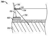
도 6은 광이 광기전력 활성 재료의 전방 혹은 앞쪽에 있는 전내부반사면으로부터 주로 전내부반사되게끔 광을 반사시키도록 구성된 도체 상에 미세구조체를 지닌 광기전력 장치의 일 실시형태의 개략 단면도;
도 7은 방향이 변화된 광이 광기전력 재료에 주로 입사되게끔 광선의 방향을 변화시키도록 구성된 도체의 전방에 표면을 지닌 광기전력 장치의 일 실시형태의 개략 단면도;
도 8은 모듈에서의 광기전력 전지의 모듈 내의 광기전력 전지의 도체 상에 혹은 해당 도체 전방에 형성된 확산체(diffuser)를 지닌 광기전력 장치의 일 실시형태의 개략 단면도;
도 9는 미세구조체로부터 반사된 일부의 광이 이어서 광기전력 재료 쪽으로 다시 향하게끔 미세구조체의 전방 및 전내부반사면의 후방에 산란체 표면 혹은 요소를 지닌 광기전력 장치의 일 실시형태의 개략 단면도;
도 10은 광기전력 전지의 어레이 내의 광기전력 전지 사이의 간극의 전방에 형성된 확산체를 지닌 광기전력 모듈의 일 실시형태의 개략 단면도;
도 11은 효율이 향상된 광기전력 모듈을 제조하기 위한 공정 흐름도.1 and 2 are schematic plan and isometric cross-sectional views illustrating one example of a solar photovoltaic device having visible reflective electrodes on the front side;
3 is a schematic illustration of two photovoltaic cells connected by tabs or ribbons;
4 is a schematic plan view of a module of a photovoltaic cell;
5 is a schematic plan view of a thin film photovoltaic module;
FIG. 6 is a schematic cross-sectional view of an embodiment of a photovoltaic device having a microstructure on a conductor configured to reflect light such that the light is primarily reflected internally from the total internal reflection surface in front of or in front of the photovoltaic active material.
7 is a schematic cross-sectional view of one embodiment of a photovoltaic device having a surface in front of a conductor configured to change the direction of the light beam such that the redirected light is primarily incident on the photovoltaic material;
8 is a schematic cross-sectional view of one embodiment of a photovoltaic device having a diffuser formed on or in front of a conductor of a photovoltaic cell in the module of the photovoltaic cell in the module;
9 is a schematic cross-sectional view of one embodiment of a photovoltaic device having scatterer surfaces or elements at the front of the microstructure and behind the total internal reflecting surface such that some light reflected from the microstructure is then directed back towards the photovoltaic material.
10 is a schematic cross-sectional view of one embodiment of a photovoltaic module with a diffuser formed in front of the gap between the photovoltaic cells in the array of photovoltaic cells.
11 is a process flow diagram for manufacturing a photovoltaic module having improved efficiency.
전형적인 광기전력 장치는 광 에너지를 전기 에너지 혹은 전류로 변환시킬 수 있다. 광기전력 장치는 적은 탄소 발자국(carbon footprint)을 지니는 동시에 환경에 대한 영향이 낮은 재생가능한 에너지원의 일례이다. 광기전력 장치를 이용하는 것은 에너지 발전 비용을 저감할 수 있어, 가능한 비용 혜택을 제공할 수 있다. 광기전력 장치는 예를 들어 우표보다 작은 크기에서부터 수 인치에 이르는 많은 상이한 크기와 형상을 지닐 수 있다. 수개의 광기전력 장치는 경우에 따라 함께 접속되어 수 피트 길이 및 수 피트 폭까지에 이를 수 있는 광기전력 모듈을 형성할 수 있다. 모듈은 또한 조합되고 접속되어 상이한 크기 및 전력 출력을 지니는 광기전력 어레이를 형성할 수 있다.Typical photovoltaic devices can convert light energy into electrical energy or current. Photovoltaic devices are an example of a renewable energy source that has a low carbon footprint and low environmental impact. Using photovoltaic devices can reduce energy generation costs, providing possible cost benefits. Photovoltaic devices can have many different sizes and shapes, for example, from smaller than a stamp to several inches. Several photovoltaic devices may optionally be connected together to form a photovoltaic module that can be up to several feet long and several feet wide. The modules can also be combined and connected to form photovoltaic arrays having different sizes and power outputs.
특정 상황에 적용되는 어레이의 크기는, 특정 위치에 이용가능한 태양광의 양 및 소비자의 요구 등과 같은 수개의 인자에 따라 조정될 수 있다. 어레이의 모듈은 전기 접속부, 장착 하드웨어, 전력 조정 장비 및 태양이 비치지 않을 때 이용하기 위한 태양 에너지를 축적하고 있는 배터리를 포함할 수 있다. 광기전력 장치는 그의 수반하는 전기접속부와 주변부를 지닌 단일의 전지, 혹은 광기전력 모듈 혹은 광기전력 어레이일 수 있다. 광기전력 장치는 또한 기능적으로 연관이 없는 전기 부품, 예컨대, 광기전력 장치(들)에 의해 통전되는 부품도 포함할 수 있다.The size of the array that applies to a particular situation can be adjusted depending on several factors, such as the amount of sunlight available at a particular location and the needs of the consumer. Modules in the array may include electrical connections, mounting hardware, power conditioning equipment, and a battery that accumulates solar energy for use when the sun is not shining. The photovoltaic device may be a single cell, or photovoltaic module or photovoltaic array, with its accompanying electrical connections and peripherals. Photovoltaic devices may also include functionally unrelated electrical components, such as components energized by photovoltaic device (s).
결정성 실리콘 웨이퍼에 의거한 현행의 태양 전지(및 보다 작은 정도의 비정질 박막 태양 전지)는 해당 전지의 전면(front surface) 상에 물리적으로 배치되어 광전류-발생 기판 재료에 전기적으로 접속된 도체의 네트워크를 이용한다. 상기 도체는 광기전력 장치(박막 광기전력 장치를 포함함)의 광기전력 재료 위에 형성된 전극일 수 있거나 혹은 도체는 모듈 및/또는 어레이 내에서 개별의 소자들을 함께 접속하는 탭(리본)일 수 있다. 광기전력 활성 재료에 유입되는 광자는 해당 재료의 전체에 걸쳐서(위에 놓인 도체 밑의 가려진 영역을 제외) 캐리어(carrier)를 발생시킨다. 음 및 양으로 하전된 캐리어(각각 전자 및 정공)는, 일단 발생되면, 캐리어가 기판 내의 결함부에 의해 포획되기 전에 광기전력 활성 재료를 통해서 제한된 거리만 주행할 수 있거나, 재결합되어 비하전된 중성 상태로 되돌아갈 수 있다. 따라서, 광-발생 전류가 광기전력 장치의 가장자리부에서만 모인 경우, 매우 작은 전류가 수집되게 된다. 위에 놓인 전도성 캐리어의 네트워크는 광기전력 장치의 실질적으로 전체 표면에 걸쳐서 전류를 수집함으로써 이 문제를 해소한다. 대부분의 캐리어는 광기전력 장치의 표면 전체에 걸쳐서 상대적으로 밀접한 간격에서 비교적 얇은 라인으로 수집될 것이고, 이들 얇은 라인으로부터 조합된 전류는 소수의 드문드문 이간된 보다 넓은 폭의 버스 라인을 통해서 광기전력 장치의 가장자리부로 흐른다.Current solar cells (and smaller degrees of amorphous thin film solar cells) based on crystalline silicon wafers are networks of conductors physically disposed on the front surface of the cell and electrically connected to the photocurrent-generating substrate material. Use The conductor may be an electrode formed on the photovoltaic material of a photovoltaic device (including thin film photovoltaic devices) or the conductor may be a tab (ribbon) that connects the individual elements together in a module and / or array. Photons entering the photovoltaic active material generate carriers throughout the material (except for the masked area underneath the underlying conductor). Negative and positively charged carriers (electrons and holes, respectively), once generated, may only travel a limited distance through the photovoltaic active material before the carrier is trapped by defects in the substrate, or may be recombined and uncharged neutral You can return to the state. Thus, if the photo-generated current is only collected at the edge of the photovoltaic device, very small currents will be collected. Overlying networks of conductive carriers solve this problem by collecting current over substantially the entire surface of the photovoltaic device. Most carriers will be collected in relatively thin lines at relatively close intervals throughout the surface of the photovoltaic device, and the combined current from these thin lines will pass through a few sparse, wider, wider bus lines. Flows to the edge of the
공교롭게도, 전도성 라인의 크기와 발생될 수 있는 광전류의 양 간에 고유의 트레이드-오프(trade-off)가 있다. 라인이 보다 작아짐에 따라, 옴 손실(ohmic losse)이 증가하고, 광기전력 장치의 출력 전압이 감소한다. 라인이 보다 커짐에 따라, 더 큰 장치 표면적이 커버되고, 더 많은 입사광이 광기전력 장치로부터 멀리 반사되어, 발생된 캐리어의 전체 수가 감소되어서, 전류 출력이 떨어진다. 최종 형태는 최적화를 통해서 결정될 수 있고, 이때 얻어지는 광전류 퍼센트는 위에 놓인 도체 어레이로 인해 손실된다.Unfortunately, there is an inherent trade-off between the size of the conductive line and the amount of photocurrent that can be generated. As the line gets smaller, the ohmic losse increases and the output voltage of the photovoltaic device decreases. As the line gets larger, the larger device surface area is covered, and more incident light is reflected away from the photovoltaic device, reducing the total number of carriers generated, resulting in a drop in current output. The final shape can be determined through optimization, and the resulting photocurrent percentage is lost due to the overlying conductor array.
도체로 인한 비교적 작은 퍼센트의 표면 손실은 중요하지 않은 것처럼 보일 수도 있지만, 이 손실은 적어도 두 가지 이유로 태양 전지 맥락에서 중요해진다. 첫번째로, 태양 전지 사업 모델은 장기간에 걸쳐 감가 상각되는 태양 전지 비용에 의존한다. 전지 효율의 비교적 작은 증가는 감가상각 시간에 커다란 영향을 미칠 수 있다. 두번째로, 태양 전지 제조라인은 매우 비용이 많이 들고, 커다란 성능 향상은 매우 값비싼 업그레이드를 불러일으킨다. 현행 공장에서 구현될 수 있는 (전도성 리드와 연관된 손실 정도에 대한) 작은 향상은 고도로 가치가 있다. 따라서, 도체로 인한 반사/흡수 손실을 제거 혹은 저감시키는 것은 태양 전지 성능에 대한 중요한 향상일 수 있다. 반사의 저감은 또한 광기전력 장치, 광기전력 전지 및 광기전력 모듈의 심미성을 향상시킬 수 있다.A relatively small percentage of surface loss due to the conductor may seem insignificant, but this loss becomes important in the solar cell context for at least two reasons. First, the solar cell business model relies on solar cell costs that are depreciated over time. A relatively small increase in cell efficiency can have a significant impact on depreciation time. Secondly, solar cell manufacturing lines are very expensive, and large performance improvements result in very expensive upgrades. Small improvements (to the extent of losses associated with conductive leads) that can be implemented in current plants are highly valuable. Thus, eliminating or reducing reflection / absorption losses due to conductors can be a significant improvement on solar cell performance. Reduction of reflection can also improve the aesthetics of photovoltaic devices, photovoltaic cells and photovoltaic modules.
광기전력(PV) 장치의 광범위한 채용 및 광 에너지를 전기 에너지로 변환시키기 위한 구조적 표면 상에 이들 장치의 배치를 저해하는 하나의 쟁점은 광기전력 장치의 전방 도체 혹은 전극의 바람직하지 않은 심미적 외관이다. 통상의 전방 전극 재료의 높은 반사율은 활성 광기전력 재료 자체의 보다 어두운 외관과 대조되고, 또한 광기전력 장치의 주변 재료와의 배합을 저해한다. 전방 전극 혹은 도체로부터의 반사는 또한 태양 전지를 비롯한 광기전력 장치의 효율을 20%까지 저감시키거나, 또는 더 많은 광기전력 장치가 반사성 전극으로 덮일 수 있다. 예를 들어, 도체는 어떤 경우에는 광기전력 장치 표면적(전면, 광입사측 상)의 10% 내지 20% 사이의 어디든지 구성할 수 있다. 본 명세서에 기재된 실시형태는, 본 명세서에 기재된 바와 같이, 다양한 방식으로 광의 방향을 변화시키기 위하여 각종 표면 상에 형성되거나 부피 내에 형성되는 미세구조체를 포함하는 확산체, 홀로그램 및 회절광학소자 등과 같은 광학 요소를 이용한다. 이러한 광학 요소는, 그렇지 않으면 수개의 광기전력 전지를 접속하여 모듈을 형성하는데 이용되는 그리드라인(gridline) 혹은 버스 전극 혹은 탭 혹은 리본 등과 같은 반사성 도체에 의해 반사될 수도 있는 광기전력 장치에 입사하는 광을 포획함으로써 광기전력 장치의 효율을 향상시킬 수 있다. 각종 기재된 실시형태는 광기전력 장치에 의한 광의 포획을 증가시킬 수 있고, 이에 따라 반사성 도체로부터 반사되는 광의 저감으로 인해 효율 및 심미성을 증가시킬 수 있다.One issue that hinders the widespread adoption of photovoltaic (PV) devices and the placement of these devices on structural surfaces for converting light energy into electrical energy is the undesirable aesthetic appearance of the front conductors or electrodes of the photovoltaic device. The high reflectance of conventional front electrode materials contrasts with the darker appearance of the active photovoltaic material itself and also hinders blending with the surrounding materials of the photovoltaic device. Reflections from the front electrode or conductor may also reduce the efficiency of photovoltaic devices, including solar cells, by 20%, or more photovoltaic devices may be covered with reflective electrodes. For example, the conductor may in some cases constitute anywhere between 10% and 20% of the surface area of the photovoltaic device (front, on the light incident side). Embodiments described herein are optical, such as diffusers, holograms and diffractive optics, including microstructures formed on various surfaces or formed in volume to vary the direction of light in various ways, as described herein. Use elements Such optical elements are light incident on photovoltaic devices that may otherwise be reflected by gridlines or bus electrodes or reflective conductors such as tabs or ribbons used to connect several photovoltaic cells to form a module. By trapping the efficiency of the photovoltaic device can be improved. Various described embodiments can increase the capture of light by the photovoltaic device, thereby increasing efficiency and aesthetics due to the reduction of light reflected from the reflective conductor.
소정의 바람직한 실시형태 및 실시예가 여기에 개시되어 있지만, 본 발명의 주제는 구체적으로 개시된 실시형태를 넘어 본 발명의 다른 대안적인 실시형태 및/또는 용도와 그의 명백한 변형과 등가물까지도 확대하여 해석할 수 있는 것으로 이해된다. 본 명세서에 개시된 발명의 범위는 특별히 개시된 실시형태로 제한되지 않도록 의도되어 있다. 이와 같이 해서, 예를 들어, 본 명세서에 개시된 소정의 방법 혹은 공정에 있어서, 당해 방법/공정을 구성하는 행위 혹은 동작은 임의의 적절한 수순으로 수행될 수 있고, 반드시 임의의 특별히 개시된 수순으로 제한될 필요는 없다. 각 실시형태의 각종 측면과 이점은 필요한 경우 기술되어 있다. 그러나 임의의 특정 실시형태에 따라서 이러한 모든 측면이나 이점들이 반드시 달성될 필요가 없는 것임을 이해할 필요가 있다. 따라서, 예를 들어, 각종 실시형태는 본 명세서에서 교시되거나 제시될 수 있는 바와 같은 기타 측면이나 이점들을 반드시 달성하지 않더라도 여기에 교시된 하나의 이점 혹은 이점군을 달성하거나 최적화하는 방식으로 수행될 수 있다는 것을 인식할 필요가 있다. 이하의 상세한 설명은 본 발명의 소정의 구체적인 실시형태에 관한 것이다. 그러나, 본 발명은 많은 다양한 방법으로 구체화될 수 있다. 본 명세서에 기재된 실시형태는 광의 대역 광자 에너지의 수집 및 그의 전기로의 변환을 위한 광기전력 장치를 포함하는 광범위한 장치에서 구현될 수 있다.While certain preferred embodiments and examples are disclosed herein, the subject matter of the present invention may be extended beyond the specifically disclosed embodiments to other alternative embodiments and / or uses of the present invention and obvious variations and equivalents thereof. It is understood that there is. It is intended that the scope of the inventions disclosed herein is not limited to the specifically disclosed embodiments. In this manner, for example, in any method or process disclosed herein, the acts or operations constituting the method / process may be performed in any suitable order and must necessarily be limited to any specially disclosed procedure. There is no need. Various aspects and advantages of each embodiment are described where necessary. However, it is to be understood that all these aspects or advantages need not necessarily be achieved, in accordance with any particular embodiment. Thus, for example, various embodiments may be performed in a manner that achieves or optimizes one advantage or group of advantages taught herein without necessarily achieving other aspects or advantages as taught or suggested herein. It is necessary to recognize that there is. The following detailed description relates to certain specific embodiments of the present invention. However, the present invention can be embodied in many different ways. Embodiments described herein can be implemented in a wide variety of devices, including photovoltaic devices for the collection of band photon energy of light and its conversion to electricity.
이 설명에서는, 전체에 걸쳐서 마찬가지 부분이 마찬가지 부호로 표기되어 있는 도면을 참조하고 있지만, 이하의 설명으로부터 명백한 바와 같이, 각 실시형태는 광기전력 활성 재료를 포함하는 다양한 장치에서 구현될 수 있다.In this description, reference is made to the drawings in which like parts are designated by like reference numerals throughout, but as is apparent from the following description, each embodiment can be implemented in various devices including photovoltaic active materials.
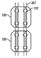
도 1 및 도 2는 전면 측 상에 가시성 반사 전극을 구비한 광기전력 장치의 일례를 도시한 개략도 및 등각투영 단면도이다. 도 1 및 도 2에 예시된 바와 같이, 많은 광기전력 장치(100)가 해당 광기전력 장치의 배면 측뿐만 아니라 해당 장치의 전면 측(201)(광이 입사되는 측) 상에 거울같은 반사성 도체(101), (102), (103)를 이용한다. 광입사 혹은 전면 측(201) 상의 도체는 보다 큰 버스 전극(102) 및/또는 보다 작은 그리드라인 전극(102)을 포함할 수 있다. 버스 전극(101)은 또한 리본(301) 혹은 탭을 땜납하거나 혹은 전기적으로 접속하기 위한 보다 큰 패드(103)를 포함할 수 있다. 리본(301)은 다수의 광기전력 장치 혹은 전지를 전기적으로 접속하여 어레이 혹은 모듈(도 3 및 도 4 참조)을 형성하는데 이용될 수 있다. 광기전력 활성 재료(203)의 전면이 조명되면, 광자는 활성 영역에서 에너지를 전자로 이행시킨다. 광자에 의해 이행된 에너지가 반도체 재료의 밴드갭보다 크다면, 전자는 그 전도대에 유입되기에 충분한 에너지를 지닐 수 있어, 결과적으로 전도대에 전자가 유입되고 전자 대신에 "정공"이 남게 된다. 내부 전계는 p-n 접합부의 형성에 의해 형성된다. 내부 전계는 에너지화된 전자(및 정공)에 작용하여 이들 전자(및 정공)가 이동함으로써 외부 회로에의 전류 흐름을 발생한다. 얻어지는 전류 흐름은 각종 전기 장치를 통전시키거나 그리드에 대해서 분포시키기 위한 전기를 발생시키는데 이용될 수 있다. 이들 전자와 정공은 도 2에 도시된 바와 같이 전면 전극(예를 들어 버스 전극(101) 혹은 그리드라인 전극(102)) 혹은 배면 전극(202)의 한쪽 혹은 다른쪽으로 이동함으로써 전류를 발생할 수 있다. 전극(101), (102)은 전극에 도달하는 전자 혹은 정공의 주행 거리를 저감하는 한편 광이 광기전력 활성층(들)으로 통과하기에 충분하도록 패턴화되어 있다. 그러나, 전면 전극(101), (102)은 광을 반사할 수 있어, 해당 광은 광전류 혹은 광전압을 발생시키는데 이용되지 않게 되고, 따라서, 광기전력 장치의 효율을 저감시킨다. 마찬가지로, 전면 도체는 종종 매력이 없는 것으로 여겨지는 밝은 반사 라인을 초래할 수 있으므로, 광기전력 장치는 종종 가시적인 위치에서 이용되지 않는다.1 and 2 are schematic and isometric cross-sectional views illustrating one example of a photovoltaic device with visible reflective electrodes on its front side. As illustrated in FIGS. 1 and 2, many
도 2에 예시된 바와 같이, 광기전력 장치는 전면 전극(101), (102)과 배면 전극(202) 사이에 배치된 광기전력 활성 영역 혹은 광기전력 활성 재료(203)를 포함할 수 있다. 몇몇 실시형태에서, 광기전력 장치(100)는 층들의 적층부가 상부에 형성되는 기판을 포함할 수 있다. 광기전력 장치(100)의 광기전력 활성 재료(203)는 실리콘 등과 같은 반도체 재료를 포함할 수 있다. 몇몇 실시형태에서, 광기전력 활성 재료(203)는 도 2에 도시된 바와 같이 n-형 반도체 재료(204)와 p-형 반도체 재료(205)를 접촉시킴으로써 형성된 p-n 접합부를 포함할 수 있다. 이러한 p-n 접합부는 다이오드 형상 특성을 지닐 수 있고 따라서 포도다이오드 구조체라고도 지칭될 수 있다.As illustrated in FIG. 2, the photovoltaic device may include a photovoltaic active region or photovoltaic
광기전력 활성층(들)(n-형 반도체 재료(204)와 p-형 반도체 재료(205)를 포함하는 바와 같이 예시됨)은 전면 전극(101), (102)과 배면 전극(202) 사이에 샌드위치되어 있다. 도 2는 전면 전극(101), (102)으로의 전자의 흐름과 배면 전극(202)으로의 "정공"의 흐름을 예시하는 한편, p-n 접합부는 전자 및 정공의 흐름이 또한 역으로 되도록 역전될 수 있었다는 것을 이해할 수 있다. 또, 재료가 n-형 반도체인지 p-형 반도체인지는 이용되는 재료 및 이들 재료의 특성에 의존하는 것도 이해할 수 있다. 전면 전극(101), (102)과 배면 전극(202)은 알루미늄, 은 혹은 몰리브덴, 또는 기타 몇몇 전도성 재료로 형성될 수 있다. 전면 전극(101), (102)은 접촉 저항을 낮추고 수집 효율을 증대시키도록 p-n 접합부의 전면의 상당한 부분을 덮도록 설계되어 있다. 전면 전극(101), (102)이 불투명한 재료로 형성되어 있는 실시형태에서, 전면 전극(101), (102)은 광기전력 활성 재료(203)의 전면에 대해서 개구부를 남겨 조명이 광기전력 활성 재료(203)에 충돌할 수 있도록 구성되어 있다. 몇몇 실시형태에서, 전면 전극(101), (102)은 투명한 도체, 예를 들어, 주석 산화물(SnO2) 또는 인듐 주석 산화물(ITO) 등의 투명 전도성 산화물(TCO: transparent conducting oxide)을 포함할 수 있다. TCO는 양호한 전기 접촉 및 전도도를 제공하는 동시에 입력광에 대해서 비교적 투명할 수 있다. TCO는 결코 완전히 투명하지 않고, TCO에 대한 전도도 대 투과율의 설계 최적화는 반사성 전극의 경우에 마치 면적 커버리지 대 전도도의 트레이드오프가 실행되는 것처럼 수행될 필요가 있음을 이해할 수 있을 것이다. 몇몇 실시형태에서, 상기 광기전력 장치는 또한 전면 전극(101), (102)에 대해서 배치된 반사방지(AR) 코팅층을 포함할 수 있다. AR 코팅층은 광기전력 장치의 전면으로부터 반사되는 광량을 저감시킬 수 있다.The photovoltaic active layer (s) (illustrated as including n-
몇몇 실시형태에서, 도 2에 도시된 p-n 접합부는 p-형 반도체와 n-형 반도체 사이에 진성 혹은 미도핑된 반도체층이 샌드위치되어 있는 p-i-n 접합부에 의해 대체될 수 있다. p-i-n 접합부는 p-n 접합부보다 높은 효율을 지닐 수 있다. 몇몇 기타 실시형태에 있어서, 광기전력 장치는 다수의 접합부를 포함할 수 있다.In some embodiments, the p-n junction shown in FIG. 2 may be replaced by a p-i-n junction in which an intrinsic or undoped semiconductor layer is sandwiched between the p-type semiconductor and the n-type semiconductor. The p-i-n junction may have higher efficiency than the p-n junction. In some other embodiments, the photovoltaic device can include multiple junctions.
광기전력 활성층(들)은 다양한 흡광성의 광기전력 활성 재료, 예컨대, 결정성 실리콘(c-실리콘), 비정질 실리콘(α-실리콘), 카드뮴 텔루르화물(CdTe), 구리 인듐 이셀렌화물(CIS), 구리 인듐 갈륨 이셀렌화물(CIGS), 흡광성 안료 및 폴리머, 흡광성 나노입자가 분산된 폴리머, GaAs 등의 III-V 반도체의 어느 것으로도 형성될 수 있지만, 기타 재료도 이용될 수 있다. 광자가 흡수되어 에너지를 전기 캐리어(정공 및 전자)로 수송하는 흡광성 재료(들)는 여기서는 광기전력 장치(100)의 광기전력 활성 재료(203)라 지칭되고, 이 용어는 다수의 활성 서브층(active sublayer)을 망라하는 것을 의미한다. 광기전력 활성층(들)의 재료는 광기전력 장치(100)의 소망의 성능과 용도에 따라 채택될 수 있다.The photovoltaic active layer (s) can be a variety of light absorbing photovoltaic active materials, such as crystalline silicon (c-silicon), amorphous silicon (α-silicon), cadmium telluride (CdTe), copper indium selenide (CIS), Copper indium gallium iselenide (CIGS), light absorbing pigments and polymers, polymers in which the light absorbing nanoparticles are dispersed, GaAs and the like can be formed of any of III-V semiconductors, but other materials may also be used. The light absorbing material (s) that absorb photons and transport energy to electrical carriers (holes and electrons) is referred to herein as the photovoltaic
몇몇 실시형태에서, 광기전력 장치(100)는 박막 기술(예시 생략)을 이용해서 형성될 수 있다. 예를 들어, 일 실시형태에서, 광 에너지가 투명한 기판을 통과할 경우, 광기전력 장치(100)는 투명 기판의 배면 위에 제1 혹은 전면 전극층(예컨대, TCO)을 증착시킴으로써 형성될 수 있다. 즉, 전면 전극은 투명한 기판 뒤쪽에, 즉, 광입사측과는 반대쪽에 있는 투명 기판의 표면 상에 형성되는 것을 의미한다. 광기전력 활성 재료(203)는 이어서 제1전극층 위에(뒤쪽에) 적층된다. 제2전극층은 광기전력 활성 재료의 층 위에(뒤쪽에) 적층될 수 있다. 이들 층은 물리적 기상 증착기술, 화학적 기상 증착기술, 전기-화학적 기상 증착기술 등을 이용해서 증착될 수 있다. 박막 광기전력 장치는 박막 실리콘, CIS, CdTe 혹은 CIGS 등의 비정질 혹은 다결정성 재료를 포함할 수 있지만, 기타 재료가 이용될 수도 있다. 박막 광기전력 장치의 몇몇 이점은 특히 제조 공정의 규모가변성(scalability) 및 작은 장치 공간(small device footprint)이다.In some embodiments,
도 3은 탭 혹은 리본(301)에 의해 접속된 2개의 광기전력 장치(100)를 개략적으로 도시하고 있다. 리본(301)은 다수의 광기전력 장치(100), 전지, 다이 혹은 웨이퍼에 대해서 버스 전극(101) 혹은 기타 전극을 접속하여 광기전력 모듈(도 4 참조)을 형성하고, 이것은 용도에 따라 요망될 수 있는 바와 같이 다수의 광기전력 장치(100)의 전압 기여를 부가함으로써 출력 전압을 증가시킬 수 있다. 리본(301)은 구리 혹은 기타 고도의 전도성 재료로 제조될 수 있다. 이 리본(301)은 버스 전극(101) 혹은 그리드라인 전극(102)과 마찬가지로, 광을 반사할 수 있고, 따라서 광기전력 장치(100)의 효율을 저감시킬 수 있다. 그러므로, 이하에 개시된 실시형태는 광기전력 장치(100)의 전방 측(201) 상에 리본(301) 혹은 소정의 도체에 적용될 수 있어, 광이 광기전력 활성 재료(203)에 도달하여 에너지 손실을 일으키는 것을 방지할 수 있다.3 schematically depicts two
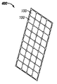
도 4는 광기전력 모듈(400)을 형성하도록 배열된 다수의 광기전력 전지의 개략 평면도이다. 상기 모듈을 구성하는 광기전력 전지는 도 1 내지 도 3에 도시된 것과 마찬가지의 광기전력 장치(100)를 포함할 수 있다. 앞서 언급된 바와 같이, 버스 전극(101), 그리드라인 전극(102), 패드(103) 및 리본(301)은 광을 반사시켜 전기로 변환하는데 이용되지 않게 할 수 있다. 그러므로, 광기전력 모듈(400)의 전체 성능이 이들 반사로 인해 저감될 수 있다.4 is a schematic top view of a plurality of photovoltaic cells arranged to form a
광기전력 모듈(400)은 해당 모듈(400)에 포함되는 다수의 광기전력 전지의 패키징에 있어서 다수의 층을 포함할 수 있다. 이들 층은 광기전력 장치(100)의 전방에 있는 커버글라스를 포함할 수 있다. 이 글라스 뒤쪽에는 광기전력 장치(100) 혹은 전지용의 봉합 재료로서 에틸렌 비닐 아세테이트(EVA 혹은 아세테이트로도 공지됨)를 포함할 수 있다. 따라서, EVA는, 몇몇 실시형태에서, 광기전력 장치(100) 뒤쪽뿐만 아니라 앞쪽에도 층을 형성할 수 있다. 폴리불화비닐(테들라; Tedlar) 백시트(backsheet)가 EVA-봉합된 광기전력 장치(100) 뒤쪽에 형성되어 광기전력 모듈(400)을 형성할 수 있다. 몇몇 실시형태에서, 커버 글라스, EVA-봉합된 광기전력 장치(100)(리본과 함께 전기적으로 접속됨) 및 테들라 시트는 알루미늄 프레임 등과 같은 금속성 프레임에 의해 가장자리부 상에 형성될 수 있다. 광기전력 모듈(400)의 패키징의 기타 방법도 가능하다.The
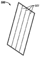
도 5는 박막 광기전력 모듈(500)의 개략 평면도이다. 몇몇 실시형태에서, 박막 광기전력 모듈(500)은 단일 모듈로서 모놀리식으로 집적될 수 있고, 따라서, 전기적으로 접속된 광기전력 전지(100)의 어레이(도 4에 예시됨)를 포함하지 않을 수 있다. 이러한 실시형태에서, 박막 광기전력 모듈(500)은 광기전력 전지보다 표면 상에 보다 적은 수의 도체를 이용할 수 있고, 따라서 보다 적은 광이 도체로부터의 반사로 인해 손실될 수 있다. 박막 광기전력 모듈(500)은 박막 광기전력 모듈(500)을 구성하는 박막 광기전력 재료 위에 형성된, 투명한 전도성 재료, 예컨대 투명한 전도성 산화물(TCO)층의 이용으로 인해 비교적 적은 수의 반사성 도체를 지닐 수 있다. 통상의 TCO로는 인듐 주석 산화물(ITO)을 들 수 있고, TCO층은 박막 광기전력 모듈(500)의 전면 전체에 걸쳐 형성된 그리드라인 전극(102)의 필요성을 저감시킬 수 있다. 그러나, 도 5에 도시된 바와 같이, 박막 광기전력 모듈(500)도 박막 광기전력 모듈(500)의 효율 및 심미성을 저감시킬 수 있는 반사성 버스 도체라인(501)을 포함할 수 있다. 실제로, 본 명세서에 개시된 효율의 향상으로 인해, 박막 광기전력 모듈(500)의 최적화는 이제 박막 광기전력 모듈(500)의 전방에 더 많은 도체(예컨대, 버스 전극)를 형성하게 되어 옴 손실을 저감하면서 반사로 인한 손실도 저감시킬 수 있게 된다.5 is a schematic top view of a thin film
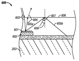
도 6은 미세구조체(601)에 충돌하는 광의 실질적인 부분이 이어서 전내부반사되는 방식으로 광을 반사하도록 구성된 미세구조체(601)를 지니는 광기전력 장치(600)의 일 실시형태의 개략 단면도이다. 각종 실시형태에서, 미세구조체(601)는 확산체의 확산 구성부, 광 산란체, 혹은 회절광학소자의 회절 구성부, 예컨대 회절 격자 혹은 홀로그램의 확산 구성부를 포함할 수 있다. 미세구조체(601)는, 몇몇 실시형태에서, 평면 혹은 입체 홀로그램을 포함할 수 있다. 몇몇 실시형태에서, 미세구조체(601)는 블레이즈 회절 격자(blazed diffraction grating)를 포함한다. 블레이즈 격자는 1차 회절이 소정 각도에서 회절되고 이어서 해당 1차 회절이 전내부반사되도록 설계되어 있다. 블레이즈 격자는, 밀접하게 이간된 지붕형상 구조체 혹은 톱니형상 격자 등과 같이, 밀접하게 이간되어 주기적인 경사를 이루는 다우의 구조체로 형성될 수 있다. 몇몇 실시형태에서, 미세구조체(601)는 도체(602) 상에 형성될 수 있거나, 혹은 도체(602) 위에 혹은 앞쪽에 형성되는 광학층 상에 형성되어 있을 수 있다. 도체(602)는 그렇지 않을 경우 광기전력 장치(100)의 광기전력 활성 재료(203)에 의해 흡수되어 버릴 수도 있었던 광을 반사시키는 광기전력 장치(100)와 연관된 도체이면 어느 것이라도 가능하다. 예를 들어, 도체(602)는 버스 전극(101), 그리드라인 전극(102), 패드(103), 리본(301) , 버스 도체라인(501) 혹은 TCO 전극을 포함할 수 있다. TCO 전극은, 박막 용도에서 특히 유용할 수 있지만, 해당 전극은 특별히 TCO 재료의 전도성이 계속해서 향상되는 바와 같은 기타 광기전력 용도에서 그 이용을 발견할 수 있다. 예시적인 실시형태에서, 미세구조체(601)는 도체(602)에 적용되거나 해당 도체 상에 형성되는 광학 매체에서 홀로그래픽 방식으로 형성될 수 있다. 다른 실시형태에서, 미세구조체(601)는, 예를 들어, 반사성 도체의 마이크로 엠보싱, 마이크로 에칭 및 플라즈마 에칭 등과 같은 처리를 이용해서 형성될 수 있다. 대안적인 실시형태에서, 감광성 재료가 도체(602) 위에 형성되고 이어서 본 명세서에 개시된 바와 같은 소망의 특성을 지니는 미세구조체(601)를 형성하도록 홀로그래픽 방식으로 노출될 수 있다. 몇몇 실시형태에서, 확산성 코팅은 양극화성 방식으로, 혹은 PVD 방식에 의해 성장되어 비평탄한 확산성 코팅을 형성할 수도 있다. 몇몇 실시형태에서, 감압식 접착제(pressure sensitive adhesive)가 산란형 미세구조체(601) 내에 형성될 수 있었다. 몇몇 실시형태에서, 각종 스핀 온 글라스(spin on glass) 재료가 실리카 입자와 혼합되어 확산성 미세구조체(601)를 형성할 수 있지만, 기타 처리도 이용될 수 있다.FIG. 6 is a schematic cross-sectional view of one embodiment of a
도 6에서 점선 화살표로 표시된 바와 같이, 도체(602)(미세구조체(601) 없음)는 광기전력 장치(100) 밖으로 유입되는 광(603)을 반사시켜, 광 에너지로 변환되어 소실되어버리는 벗어나는 광(604)을 초래한다. 그러나, 각종 실시형태에서, 미세구조체(601)는 광(605a)이 임계각(608)보다 큰 각도(607)에서 전내부반사면(606)에 충돌할 수 있도록 유입되는 광(603)을 산란, 확산 및/또는 반사시킬 수 있다. 그러므로, 광(605a)은 광기전력 활성 재료(203)로 향하여 도로 전내부반사시켜, 광선(605b) 내의 에너지의 포획 및 전기로의 변환을 허용하게 한다.As indicated by the dashed arrows in FIG. 6, the conductor 602 (without the microstructure 601) reflects the light 603 flowing out of the
도체(602)가 리본(301)을 포함하는 실시형태에서, 미세구조체(601)는 전술한 것과 마찬가지 방식으로 리본(301) 상에 형성되어 있을 수 있다. 대안적으로, 리본(301)은 반사성 도체의 마이크로 엠보싱, 마이크로 에칭 및 플라즈마 에칭 등과 같은 처리를 이용해서 수행하거나 혹은 시트 위에 감광성 재료를 형성하면서(이어서 감광성 재료에 회절광학소자, 예컨대, 홀로그램을 형성하면서) 도체의 시트를 하나의 롤에서 풀어서 다른 롤에 감음으로써 형성될 수 있다. 상기 시트는 절단되어 리본(301)을 형성할 수 있고 해당 리본은 이어서 다수의 광기전력 전지를 함께 전기적으로 접속하는데 이용될 수 있다. 상기 리본(301)은 전형적으로는 0.08㎜ 내지 0.3㎜의 두께와 1.5㎜ 내지 15㎜의 폭을 지닐 수 있다. 도체층의 가장자리부는 각지거나 라운드처리되어 있을 수 있다. 리본(301)의 길이는 원하는 개수의 광기전력 장치(100)를 접속할 필요가 있는 한 제조될 수 있다.In embodiments in which the
미리 제작된 리본(301)은 이어서 다수의 광기전력 장치(100)의 도체(101, 102, 103, 501)와 상호 접속되어 모듈 혹은 태양 패널 혹은 어레이를 형성할 수 있다. 당업자라면 리본(301) 상의 미세구조체(601)가 또한 예를 들어 해당 리본(301)을 플라즈마 에칭한 후에 해당 리본(301)을 땝납하여 다수의 광기전력 장치(100)를 전기적으로 접속함으로써 얻어질 수 있다는 것도 이해할 수 있을 것이다. 대안적으로, 미세구조체(601)는 임의선택적으로 이형층(도시 생략)을 지니는 테이프 기판 혹은 기타 층(도시 생략) 상에 형성되어 있을 수 있다. 미세구조체(601)는 이어서 광기전력 장치(100)에 땜납되거나 혹은 다르게는 전기적으로 접속되기 전 혹은 후에 감압식 접착제 혹은 기타 적절한 수단을 이용해서 리본(301) 상에 적층될 수 있다.The
전내부반사면(606)은 고굴절률 재료와 저굴절률 재료 사이의 임의의 계면에 형성될 수 있다. 예를 들어, 전내부반사면(606)은 임의의 광기전력 장치(100) 또는 광기전력 모듈(광기전력 모듈(400) 혹은 박막 광기전력 모듈(500) 등)의 커버 글라스와 주변 공기(혹은 기타 저굴절률 재료) 사이의 계면에 형성될 수 있다. 도 6은 도체(602) 및 광기전력 활성층(203) 위에 오직 하나의 층(예컨대, EVA 등과 같은 컨포멀 코팅(conformal coating))을 예시하고 있지만, 다수의 층이 도체(602)와 광기전력 활성층(203)의 앞쪽에 형성될 수 있다는 것을 이해할 수 있을 것이다. 예를 들어, 도체(602), 미세구조체(601) 및 광기전력 활성층(203)은 EVA 위에 커버글라스를 지니는 상태의 광기전력 장치(100) 혹은 전지용의 봉합용 재료로서 EVA 층 내에 봉합되어 있을 수 있다. 이 경우 표면(606)은, EVA와 커버 글라스의 굴절률이 유사할 수 있으므로 커버 글라스의 외표면에 위치되어 있는 것처럼 보일 것이다. 기타 봉합 재료도 이용될 수 있다. 봉합층이 그 앞에 있는 층의 굴절률보다 높은 굴절률을 지니는 경우에, 전내부반사면(606)은 해당 봉합층과 그 앞에 있는 층 사이의 계면에 형성될 것이다. 봉합층이 그 앞에 있는 층의 굴절률보다 낮은 굴절률을 지니는 경우, 전내부반사면(606)은 봉합층의 앞쪽에 있는 층의 공기 계면에 형성될 것이다. 광기전력 장치(600)는 또한 광기전력 활성 재료(203)와 도체(602) 사이의 기타 층, 예컨대, 투명한 전도성 재료층(609)을 포함할 수도 있다.The total internal reflecting
도 7은 도체(602)의 전방에 표면(701)을 지니는 광기전력 장치(700)의 일 실시형태의 개략 단면도로, 상기 표면(701)은 방향이 변화된 광(703)의 일부가 광기전력 활성 재료(203)에 입사되게끔 입사광선(702)의 방향을 변화시키도록 구성되어 있다. 각종 실시형태에서, 상기 표면(701)은 확산체 혹은 홀로그램을 포함할 수 있다. "표면"이란 용어가 이용되지만, 표면(701)은, 또한 부피, 예컨대, 입체 홀로그램 혹은 주어진 두께를 지닌 층을 포함할 수도 있다는 것을 이해할 수 있을 것이다. 더욱 일반적으로, 표면(701)은 평면 혹은 입체 홀로그램, 회절광학소자, 회절 구성부, 확산체, 확산 구성부, 또는 본 명세서에 기재된 바와 같이 광을 편향 및/또는 광의 방향을 변화시키는 능력을 지니는 기타 광학 요소를 포함할 수 있다. 표면(701)은 도체(602)의 앞쪽에 형성되거나 배치되는 층(704) 상에 형성되어 있을 수 있다. 몇몇 실시형태에서, 상기 층(704)은 광기전력 장치(100)의 표면 위에 도체(602)에 의해 형성된 패턴과 실질적으로 일치 및/또는 정렬하도록 패턴화되어 있을 수 있다. 몇몇 실시형태에서, 표면(701)은 광(705)을 편향 및/또는 당해 광의 방향을 변화시켜 도체(602)에 충돌시킴으로써 재차 광기전력 활성 재료(203) 쪽으로 향하게 하므로 해당 광기전력 활성 재료(203)에 의해 흡수될 수 있게 된다. 표면(701)은, 그렇지 않다면 도체(602)에 충돌하게 될 수도 있지만, 당해 충돌하기 전에 광을 방향 변화시킴으로써, 도체(602)와 연관된 손실(반사 등)을 저감시킨다. 몇몇 실시형태에서, 도체(602)는 흡수 등과 같이, 반사 이외의 수법에 의해 손실을 일으킬 수 있다. 따라서, 도체(602)는 반사에 의해서뿐만 아니라, 흡수에 의해서도(일부의 광 에너지가 흡수에 의해 소실될 수 있는 투명 혹은 반투명한 도체에서처럼) 광 에너지의 손실을 초래할 수 있다.FIG. 7 is a schematic cross-sectional view of one embodiment of a
도 8은 광기전력 장치(100)의 도체(101 , 102, 103) 상에 혹은 당해 도체의 전방에 형성된 확산체(801)를 지닌 광기전력 모듈(800)의 일 실시형태의 개략 단면도이다. 예시된 바와 같이, 광기전력 장치(100)는 광기전력 모듈(800)(도 4의 것과 마찬가지임) 내의 광기전력 장치(100)의 어레이 내에 있다. 그러나, 확산체(801)는 광기전력 모듈 내의 전지 상에, 혹은 박막 광기전력 모듈(500) 등과 같은 모놀리식으로 일체화된 모듈 내에, 개별적인 광기전력 전지 등과 같은 임의의 광기전력 장치(100)의 도체(602) 상에 형성될 수 있다. 상기 확산체(801)는 예를 들어 홀로그램(예컨대, 홀로그래픽 확산체) 등과 같은 소망의 광학 기능을 지닌 임의의 구조체로부터 혹은 도체(602)의 표면을 조면화(roughening)함으로써 형성될 수 있다. 대안적으로, 회절 격자 등의 회절광학소자가 이용될 수 있다. 확산체(801)는 도체(602) 상에 부착될 수 있는 확산 테이프일 수도 있다. 대안적으로, 확산체(801)는 도체에 미세구조체를 부여하는 것에 부가해서 도체 상에 백색 도료 등과 같은 스프레이-온 디퓨저를 포함할 수도 있다. 기타 유형의 확산체가 이용될 수도 있다. 확산체(801)는 다수의 상이한 방향으로 광을 확산시킬 수 있다. 몇몇 실시형태에서, 확산체(801)는 180°(즉, 도체(602)의 전면에 대해서 수직으로부터 ±90°)에 걸쳐서 광을 확산시킬 수 있다. 몇몇 이러한 실시형태에서, 확산체(801)는 람베르트 확산체(Lambertian diffuser)일 수 있고, 180°에 걸쳐서 균등하게 광을 확산시킬 수 있다. 이러한 실시형태에서, 람베르트 확산체로부터 확산된 일부의 광은 전내부반사각보다 큰 각도에서 전내부반사면(606) 상에 입사하지 않을 것이며, 따라서 광기전력 장치로 도로 향하지 않게 될 것이다. 그러나, 람베르트 확산체는 전내부반사각도보다 큰 각도에서 전내부반사면(606)에 입사하도록 충분한 광을 확산시켜, 광기전력 장치의 효율을 적절하게 향상시킬 수 있다. 순수한 람베르트 표면을 제조하는 것은 주어진 현행 기술에서 어려울 수 있으므로, 다른 실시형태에서, 확산체(801)는 0°와 90°혹은 90°와 180°사이의 각도 범위에 걸쳐서 광을 확산시킬 수 있다. 많은 범위가 달성될 수 있지만, 실제의 확산체는 완벽하지 않다는 것을 이해할 수 있을 것이다. 따라서, 예를 들어 직각으로부터 ±45°보다 큰 각도에서 입사광을 확산시키도록 구성된 실제의 확산체는 이들 각도에서 모든 광을 확산시키지 않을 것이다. 각종 범위는 50% 미만의 피크 투과율이 주어진 범위 밖의 각도에서 확산(반사)되는 것을 나타내는 것을 의미하는 것임을 이해할 수 있을 것이다. 몇몇 실시형태에서, 확산체(801)는 수직으로부터 50°에서 수직으로부터 85°이상까지 적절한 광을 확산시킬 수 있다. 몇몇 실시형태에서, 전내부반사각보다 큰 각도의 소정의 범위에서 확산체(801)로부터 반사된 광의 강도는 피크 강도 각(즉, 최대 반사된 강도를 지니는 각도)에서 반사된 광 강도의 70%보다 크다. 예를 들어, 확산체(801)는 (광기전력 장치 표면의) 수직으로부터 42° 내지 55°의 범위 내의 피크 강도 각에서 반사된 광 강도의 70%보다 크거나 같은 강도에서 반사될 수 있다. 몇몇 실시형태에서, 전내부반사각보다 큰 각도의 소정의 범위에서 확산체(801)로부터 반사된 광의 강도는 피크 강도 각에서 반사된 광 강도의 50%보다 크다.8 is a schematic cross-sectional view of one embodiment of a
도 8에 예시된 바와 같이, 확산체(801)는 도체로부터 반사된 광의 일부가 전내부반사면(606)에서 전내부반사되는 것을 허용할 수 있다. 예시된 바와 같이, 전내부반사면(606)은 도체(101), (102), (103)의 전방에 형성된 커버 글라스(802)(유리판) 혹은 기타 고굴절률 판의 공기-유리 계면에 형성된다. 그러나, 상기 장치는 다른 방식으로 패키지되어 있을 수도 있다. 예시된 바와 같이, 광의 일부분은 전내부반사면(606)과 수직 혹은 거의 수직으로 반사되어 빠져나갈 수 있다. 바람직하게는, 확산체(801)는 확산된 광이 임계각보다 큰 각도에서 전내부반사면(606)에 입사되도록 실질적인 양의 광을 확산시킨다. 어느 경우에도, 순수한 람베르트 확산도 상당한 효율 향상을 가져올 수 있다. 그러므로, 확산이 비람베르트 방식(non-Lambertian)이고, 확산체(801)가 광의 보다 많은 부분이 임계각보다 큰 각도에서 전내부반사면(606)에 입사되도록 광을 확산시킬 수 있는 실시형태에서, 보다 큰 효율의 향상이 가능하다. 예를 들어, 몇몇 실시형태에서, 10% 미만의 광이 수직의 ±10° 이내에서 반사된다.As illustrated in FIG. 8, the
예시된 바와 같이, 광기전력 모듈(800)은 종종 EVA로 제조된 봉합층(803) 내에 봉합된 광기전력 장치(100)를 포함한다. 상기 광기전력 모듈(800)은 또한 백시트(804)를 포함한다. 전형적으로, 상기 층은 종종 알루미늄 등과 같은 금속으로 이루어진 프레임(805)으로 둘러싸일 것이다. 그러나, 각종 기타 실시형태에서는, 보다 많거나 적은 수의 층이 이용될 수 있고, 기타 적절한 재료가 위에서 언급된 것 대신에 교체될 수 있다.As illustrated, the
도 9는 광선(902) 등과 같이 전내부반사될 수 없는 광이 이어서 광기전력 활성 재료(203) 쪽으로 재차 향하도록 미세구조체(601)의 전방에 그리고 전내부반사면(606)의 후방에 산란체(901)를 지니는 광기전력 장치(100)의 일 실시형태의 개략 단면도이다. 예시된 바와 같이, 광기전력 장치(100)는 광기전력 모듈(900)(도 4의 것과 마찬가지임)의 광기전력 장치(100)의 어레이 내에 있다. 그러나, 산란체(901)는 광기전력 모듈 내의 전지 상에, 혹은 박막 광기전력 모듈(500) 등과 같은 모놀리식으로 일체화된 모듈 내에, 개별적인 광기전력 전지 등과 같은 임의의 광기전력 장치(100)의 전방에 형성될 수 있다. 도 8과 관련하여 위에서 언급된 바와 같이, 일부의 광은 전내부반사면에 직교하여 혹은 거의 직교하여 미세구조체(601)로부터 반사되어 빠져나갈 수 있다. 몇몇 실시형태에서, 산란체(901)는 광기전력 활성 재료(203)를 향하여 도로 거의 수직 각도로 미세구조체(601)로부터 반사된 광을 산란시키거나 재차 향하도록 미세구조체(601)의 전방에 배치된 홀로그램, 회절 격자 혹은 확산체를 포함할 수 있다. 다른 실시형태에서, 도체(602)는 미세구조체(601)를 포함하지 않을 수 있고, 반사성 도체로서 광을 반사할 수 있다. 이러한 실시형태에서, 산란체(901)는 해당 산란체(901)에 의해 반사된 광이 전기로 변환하기 위하여 광기전력 활성 재료(203)에 의해 이어서 흡수되게끔 소정 각도에서 도로 광을 반사하도록 구성되어 있을 수 있다. 산란체(901)는 또한 광기전력 활성 재료(203) 쪽으로 장치 상에 입사하는 광을 굴절, 산란 및/또는 회절하는 작용을 할 수 있다. 따라서, 산란체(901)는 투명한 재료를 포함할 수 있고, 다양한 포토그래피를 지닌 표면 혹은 굴절률의 변화를 포함할 수 있다.9 shows the scatterers in front of the
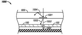
도 10은 광기전력 전지의 어레이 내의 광기전력 장치(100) 사이의 간극(1002)의 전방에 형성된 확산체(1001)를 지닌 광기전력 모듈(1000)의 일 실시형태의 개략적 단면도이다. (대시선의) 광선(1003)으로 예시된 바와 같이, 광은 간극이 어레이 내의 인접한 전지 사이에 있을 때 광기전력 장치(100) 사이의 간극 내에서 소실될 수 있다. 확산체(1001)는, 광선(1004)이 임계각보다 큰 각도에서 전내부반사면(606)에 입사하도록 광을 반사시킴으로써 그렇지 않을 경우 광 에너지를 소실할 수도 있는 그 일부를 재포획하는 것을 도울 수 있고, 그러므로 모듈(100) 내의 광기전력 장치(100) 쪽으로 도로 전내부반사될 수 있다. 확산체(1001)는 도 8과 관련하여 개시된 확산체(801)와 같은 특성을 실질적으로 지닐 수 있다. 확산체(1001)는 소망의 광학 기능, 예를 들어, 홀로그램(예컨대, 홀로그래픽 확산체) 등을 구비한 임의의 구조체로부터 형성될 수 있다. 대안적으로, 회절 격자 등과 같은 회절광학소자가 이용될 수 있다. 다른 실시형태에서, 확산체(1001)는 전내부반사를 지니지 않은 광기전력 장치(100) 쪽으로 광선(1005) 등과 같은 투과광을 편향(예컨대, 굴절)시킴으로써 그렇지 않을 경우 광 에너지를 소실할 수도 있는 그 일부를 재포획하는 것을 도울 수 있다.FIG. 10 is a schematic cross-sectional view of one embodiment of a
본 명세서에 개시된 각종 실시형태에서, 광기전력 장치의 효율이 향상될 수 있다. 예를 들어, (예컨대, 10% 내지 20%의 도체 개구를 지닌 광기전력 장치에 있어서) 도체 개구의 30% 내지 65%가 복원된다. 본 명세서에서 이용되는 바와 같이, 도체 개구는 도체에 의해 커버되는 표면적이다. 도체 개구 복원율(conductor aperture recovery)은, 그렇지 않을 경우 도체에 의해 차단되었을 광이 확산체로부터의 편향 및 노출된 활성 영역으로 도로 다시 향하게 되는 결과로서 활성 영역에 도달하기 때문에 효율적으로 회복되는 태양전지의 활성 영역의 양에 상당한다. 그러므로, 20% 도체 개구란 대신에 도체에 의해 커버되는 광에 그렇지 않을 경우 노출되게 되는 표면적의 20%를 지니는 광기전력 장치를 의미한다. 이 범위(예컨대, 6 내지 12%)에서의 도체 개구 복원율은 개구 복원율을 지니지 않은 장치에 비해서 약 6% 내지 12%의 광기전력 장치 효율의 향상을 초래할 수 있다. 몇몇 실시형태에서, 30 내지 65%의 도체 개구 복원율이 달성될 수 있다.In various embodiments disclosed herein, the efficiency of the photovoltaic device can be improved. For example, 30% to 65% of the conductor opening is restored (eg for a photovoltaic device with 10% to 20% of the conductor opening). As used herein, the conductor opening is the surface area covered by the conductor. Conductor aperture recovery is the efficiency of solar cells that recover efficiently because light that otherwise would have been blocked by the conductor would reach the active region as a result of deflection from the diffuser and back to the exposed active region. It corresponds to the amount of active area. Thus, a 20% conductor opening means instead a photovoltaic device having 20% of the surface area that would otherwise be exposed to light covered by the conductor. Conductor aperture recovery in this range (eg, 6-12%) can result in an improvement in photovoltaic device efficiency of about 6% to 12% compared to devices that do not have aperture recovery. In some embodiments, 30 to 65% conductor aperture recovery can be achieved.
도 11은 효율이 향상된 광기전력 모듈을 제조하기 위한 공정 흐름을 도시하고 있다. 도 11에 도시된 바와 같이, 스텝 1110은 광기전력 전지를 제조하는 공정을 포함한다. 이것은 필요에 따라 반도체 웨이퍼의 각종 영역을 도핑하는 단계, 해당 웨이퍼의 전면 혹은 배면에 도체와 전극을 도포하는 단계, 본 명세서의 어느 부분에선가 개시되어 있는 바와 같이 도체 및 전극 상에 미세구조체를 형성하는 단계 및 당업계에 공지된 기타 공정을 수행하는 단계를 포함할 수 있다. 스텝 1120에서, 상기 광기전력 전지에 전도성 탭이 부착된다(도 3 참조). 스텝 1130(임의선택사양)에서, 상기 전도성 탭에 광학 요소가 부착 혹은 도포된다. 해당 광학 요소는 미세구조체 및/또는 확산체(확산형 백색 도료 등과 같은 스프레이-온 디퓨저) 등과 같이 본 명세서에 개시된 요소의 어느 것이라도 포함할 수 있다. 스텝 1140에서, 상기 전지는 이어서 광기전력 모듈 내로 적층 및 조립된다. 스텝 1130은, 예시된 바와 같이, 전도성 탭을 상기 전지에 부착한 후에 수행될 수 있다. 대안적으로, 상기 전도성 탭은 미리 적용된 광학 요소를 지닐 수 있거나 혹은 해당 탭은 전처리되어 있을 수 있다. 예를 들어, 상기 전도성 탭은 당해 전도성 탭의 광 입사측 상에 미리 부착된 확산 테이프를 지닐 수 있다. 대안적으로, 상기 전도성 탭은 미세구조체로 전처리되어 있을 수 있다. 그러므로, 상기 탭이 미리 부착된 광학 요소에 딸려 있거나 혹은 다르게는 전처리되어 있을 경우, 스텝 1120은 스텝 1140을 개재하는 일없이 스텝 1140으로 이어질 수 있다. 다른 실시형태에서, 표면이 도체의 전방에 배치되어 있고, 여기서 표면은 방향이 변화된 광이 상기 도체 대신에 광기전력 재료 상에 입사되도록 상기 도체 쪽으로 향하던 입사광의 방향을 변화시키도록 구성되어 있다. 도체의 전방의 표면은, 방향이 변화된 광의 일부가 도체 대신에 예를 들어 광기전력 전지 내의 광기전력 활성 재료 상에 입사되도록 입사광선의 방향을 변화시키도록 구성되어 있다. "표면"(surface)은 평면 혹은 입체 홀로그램, 또는 상기 도 7을 참조하여 설명된 바와 같이 광을 편향시키고/시키거나 광의 방향을 변화시킬 수 있는 기타 광학 요소를 포함할 수 있다. 상기 표면은 도체의 전방에 배치되거나 형성된 층 상에 형성되어 있을 수 있고, 예를 들어, 상기 표면은 스텝 1140의 광기전력 모듈 내에 전지를 적층시키는데 이용되는 유리 및/또는 기타 재료의 일부일 수 있거나 그 위에 형성될 수 있다. 몇몇 실시형태는 광기전력 전지 혹은 모듈에서의 도체의 패턴과 실질적으로 일치, 당해 패턴과 정렬 및/또는 당해 패턴과 대응하도록 상기 표면을 패턴화하는 단계를 포함할 수 있다. 상기 표면은 전술한 바와 같은 홀로그램 혹은 기타 광학 요소를 포함하는 테이프 혹은 적층체를 포함할 수 있다. 상기 테이프 혹은 층은 전술한 바와 같이 도체의 전방(입사 측)에 놓인 유리 및/또는 기타 재료 위에 전술한 바와 같이 패턴으로 도포 혹은 적층되어 있을 수 있다. 기타 실시형태는 기계적 혹은 화학적 수단에 의해 도체의 전방에 놓인 유리 및/또는 기타 재료에 직접 표면을 형성하는 단계를 포함할 수 있다. 각종 실시형태에서, 상기 표면은, 도체의 전방에 놓인 유리 및/또는 기타 재료 상에 직접 형성되거나 테이프이거나 적층체이거나에 따라, 도체에 충돌할 광을 편향 및/또는 방향변화시켜, 광기전력 활성 재료 쪽으로 방향변화시키므로, 해당 광은 광기전력 활성 재료에 의해 흡수될 수 있다. 이와 같이 해서, 상기 표면은 도체와 연관된 손실을 저감시킨다.11 shows a process flow for manufacturing the photovoltaic module with improved efficiency. As shown in FIG. 11,
이상에서는 특정의 바람직한 실시형태 및 실시형태를 개시하였지만, 본 발명의 주제는 구체적으로 개시된 실시형태를 넘어 본 발명의 다른 대안적인 실시형태 및/또는 용도와 그의 명백한 변형과 등가물까지도 확대하여 해석할 수 있는 것으로 이해된다. 본 명세서에 개시된 발명의 범위는 특별히 개시된 실시형태로 제한되지 않도록 의도되어 있다. 이와 같이 해서, 예를 들어, 본 명세서에 개시된 소정의 방법 혹은 공정에 있어서, 당해 방법/공정을 구성하는 행위 혹은 동작은 임의의 적절한 수순으로 수행될 수 있고, 반드시 임의의 특별히 개시된 수순으로 제한될 필요는 없다. 각 실시형태의 각종 측면과 이점은 필요한 경우 기술되어 있다. 그러나 임의의 특정 실시형태에 따라서 이러한 모든 측면이나 이점들이 반드시 달성될 필요가 없는 것임을 이해할 필요가 있다. 따라서, 예를 들어, 각종 실시형태는 본 명세서에서 교시되거나 제시될 수 있는 바와 같은 기타 측면이나 이점들을 반드시 달성하지 않더라도 여기에 교시된 하나의 이점 혹은 이점군을 달성하거나 최적화하는 방식으로 수행될 수 있다는 것을 인식할 필요가 있다.While specific preferred embodiments and embodiments have been disclosed above, the subject matter of the present invention may be extended beyond the specifically disclosed embodiments to other alternative embodiments and / or uses of the present invention and obvious variations and equivalents thereof. It is understood that there is. It is intended that the scope of the inventions disclosed herein is not limited to the specifically disclosed embodiments. In this manner, for example, in any method or process disclosed herein, the acts or operations constituting the method / process may be performed in any suitable order and must necessarily be limited to any specially disclosed procedure. There is no need. Various aspects and advantages of each embodiment are described where necessary. However, it is to be understood that all these aspects or advantages need not necessarily be achieved, in accordance with any particular embodiment. Thus, for example, various embodiments may be performed in a manner that achieves or optimizes one advantage or group of advantages taught herein without necessarily achieving other aspects or advantages as taught or suggested herein. It is necessary to recognize that there is.
Claims (39)
광기전력 재료;
상기 광기전력 재료와 전기 접촉하는 도체;
상기 도체 및 상기 광기전력 재료의 전방에 배치된 전내부반사면(total-internal-reflection surface); 및
상기 전내부반사면의 후방에 있는 미세구조체(microstructure)를 포함하되,
상기 도체는 입사광을 반사시키고,
상기 미세구조체는, 적어도 일부의 반사된 광이 상기 전내부반사면의 임계각보다 큰 각도에서 해당 전내부반사면에 입사되게끔, 광을 반사시키도록 구성된 것인 광기전력 장치(photovoltaic device).A photovoltaic device having a front side on which light is incident and a rear side opposite to the front side,
Photovoltaic materials;
A conductor in electrical contact with the photovoltaic material;
A total-internal-reflection surface disposed in front of the conductor and the photovoltaic material; And
Including a microstructure behind the total internal reflection surface,
The conductor reflects incident light,
Wherein the microstructure is configured to reflect light such that at least some of the reflected light is incident on the total internal reflecting surface at an angle greater than a critical angle of the total internal reflecting surface.
입사광으로부터 전기를 발전시키는 발전수단(electricity generating means);
상기 발전수단과 전기 접촉하는, 전기를 전도하는 전도수단;
상기 전도수단 및 상기 발전수단의 전방에 배치된, 광을 전내부반사시키는 전내부반사수단; 및
상기 전내부반사수단의 후방에 있는, 광을 반사시키는 반사수단을 포함하되.
상기 전도수단은 입사광을 반사시키고,
상기 반사수단은, 적어도 일부의 반사된 광이 상기 전내부반사수단의 임계각보다 큰 각도에서 해당 전내부반사수단에 입사되게끔, 광을 반사시키도록 구성된 것인 광기전력 장치.A photovoltaic device having a front side to which light is incident and a rear side opposite to the front side,
Electricity generating means for generating electricity from incident light;
Conductive means for conducting electricity in electrical contact with the power generation means;
Total internal reflecting means for reflecting the light internally disposed in front of the conducting means and the power generating means; And
And reflecting means for reflecting light at the rear of the total internal reflecting means.
The conducting means reflects incident light,
And the reflecting means is configured to reflect light such that at least some of the reflected light is incident on the total internal reflecting means at an angle greater than a critical angle of the total internal reflecting means.
상기 전도수단이 도체를 포함하거나;
상기 전내부반사수단이 전내부반사면을 포함하거나; 또는
상기 반사수단이 미세구조체를 포함하는 것인 광기전력 장치.12. The apparatus of claim 11, wherein said power generation means comprises a photovoltaic material;
The conducting means comprises a conductor;
The total internal reflecting means comprises a total internal reflecting surface; or
Photovoltaic device wherein the reflecting means comprises a microstructure.
광기전력 재료;
상기 광기전력 재료의 전방에 있고 또한 해당 광기전력 재료와 전기 접촉하는 도체; 및
방향이 변화된 광이 상기 도체 대신에 상기 광기전력 재료로 입사되게끔 상기 도체 쪽으로 향하는 입사광선의 방향을 변화시키도록 구성된, 상기 도체의 전방에 있는 표면을 포함하는 광기전력 장치.A photovoltaic device having a front side on which light is incident and a rear side opposite to the front side,
Photovoltaic materials;
A conductor in front of the photovoltaic material and in electrical contact with the photovoltaic material; And
And a surface in front of the conductor configured to change the direction of incident light directed towards the conductor such that redirected light is incident on the photovoltaic material instead of the conductor.
입사광으로부터 전기를 발전시키는 발전수단;
상기 발전수단의 전방에 있고, 해당 발전수단과 전기 접촉하는, 전기를 전도하는 전도수단;
방향이 변화된 광이 상기 전도수단 대신에 상기 발전수단에 입사되게끔 상기 전도수단 쪽으로 향하는 입사광선의 방향을 변화시키도록 구성된 것인 광의 방향을 변화시키는 방향변화수단(redirecting means)을 포함하는 광기전력 장치.A photovoltaic device having a front side to which light is incident and a rear side opposite to the front side,
Power generation means for generating electricity from incident light;
Conducting means for conducting electricity in front of the power generating means and in electrical contact with the power generating means;
Photovoltaic power comprising redirecting means for changing the direction of light which is configured to change the direction of incident light directed toward the conducting means such that the redirected light is incident on the power generating means instead of the conducting means. Device.
상기 전도수단이 도체를 포함하거나; 또는
상기 방향변화수단이 표면을 포함하는 것인 광기전력 장치.18. The apparatus of claim 17, wherein the power generation means comprises a photovoltaic material;
The conducting means comprises a conductor; or
The photovoltaic device wherein said direction changing means comprises a surface.
광기전력 재료와 전기접촉하도록 해당 광기전력 재료에 대해서 배치된 도체를 제공하는 단계;
상기 도체와 상기 광기전력 재료의 전방에 전내부반사면을 배치하는 단계; 및
상기 전내부반사면의 후방에 미세구조체를 배치하는 단계를 포함하되,
상기 도체는 입사광을 반사시키고,
상기 미세구조체는, 적어도 일부의 반사된 광이 상기 전내부반사면의 임계각보다 큰 각도에서 상기 전내부반사면에 입사되게끔, 광을 반사시키도록 구성되어 있는 것인, 광기전력 장치의 제조방법.A method of manufacturing a photovoltaic device,
Providing a conductor disposed for the photovoltaic material in electrical contact with the photovoltaic material;
Disposing a total internal reflecting surface in front of the conductor and the photovoltaic material; And
Disposing a microstructure behind the front internal reflection surface,
The conductor reflects incident light,
Wherein the microstructure is configured to reflect light such that at least some of the reflected light is incident on the total internal reflecting surface at an angle greater than a critical angle of the total internal reflecting surface. .
광기전력 재료와 전기 접촉하도록 해당 광기전력 재료에 대해서 배치된 도체를 제공하는 단계; 및
상기 도체의 전방에 표면을 배치하는 단계를 포함하되,
상기 도체는 입사광을 반사시키고,
상기 표면은, 방향이 변화된 광이 상기 도체 대신에 상기 광기전력 재료에 입사되게끔, 상기 도체 쪽으로 향하는 입사광선의 방향을 변화시키도록 구성된 것인, 광기전력 장치의 제조방법.A method of manufacturing a photovoltaic device,
Providing a conductor disposed for the photovoltaic material in electrical contact with the photovoltaic material; And
Disposing a surface in front of the conductor,
The conductor reflects incident light,
And the surface is configured to change the direction of incident light directed towards the conductor such that the redirected light is incident on the photovoltaic material instead of the conductor.
두 부분으로 이간된 광기전력 재료 사이에 있는 간극; 및
방향이 변화된 광이 상기 간극 대신에 상기 광기전력 재료 상에 입사되게끔 상기 간극 쪽으로 향하는 입사광선의 방향을 변화시키도록 구성된 표면을 포함하는 광기전력 어레이.A photovoltaic array having a front side to which light is incident and a rear side opposite to the front side,
A gap between the photovoltaic material spaced into two parts; And
And a surface configured to change the direction of incident light directed towards the gap such that redirected light is incident on the photovoltaic material instead of the gap.
두 부분으로 이간된 발전수단 사이에 있는 간극; 및
방향이 변화된 광이 상기 간극 대신에 상기 발전수단 상에 입사되게끔, 상기 간극 쪽으로 향하는 입사광선의 방향을 변화시키도록 구성된, 상기 간극의 전방에 위치된 방향변화수단을 포함하는 광기전력 장치.A photovoltaic device having a front side to which light is incident and a rear side opposite to the front side,
A gap between the power generation means separated into two parts; And
And a direction changing means positioned in front of the gap, the direction changing means being configured to change the direction of the incident light directed toward the gap such that the changed light is incident on the power generating means instead of the gap.
상기 방향변화수단이 반사요소를 포함하거나; 또는
상기 방향변화수단이 굴절요소를 포함하는 것인 광 기전력 장치.37. The apparatus of claim 36, wherein said power generation means comprises a photovoltaic material;
The direction changing means comprises a reflecting element; or
The photovoltaic device wherein said direction change means comprises a refractive element.
이간된 광기전력 재료 사이에 있는 간극의 전방에 표면을 배치하는 단계를 포함하되,
상기 표면은 방향이 변화된 광이 상기 간극 대신에 상기 광기전력 재료 상에 입사되게끔 상기 간극 쪽으로 향하는 입사광선의 방향을 변화시키도록 구성된 것인, 광기전력 장치의 제조방법.A method of manufacturing a photovoltaic device,
Disposing a surface in front of the gap between the spaced apart photovoltaic materials,
And the surface is configured to change the direction of incident light directed towards the gap such that the redirected light is incident on the photovoltaic material instead of the gap.
Applications Claiming Priority (2)
| Application Number | Priority Date | Filing Date | Title |
|---|---|---|---|
| US4444308P | 2008-04-11 | 2008-04-11 | |
| US61/044,443 | 2008-04-11 |
Publications (1)
| Publication Number | Publication Date |
|---|---|
| KR20110000695A true KR20110000695A (en) | 2011-01-04 |
Family
ID=41162584
Family Applications (1)
| Application Number | Title | Priority Date | Filing Date |
|---|---|---|---|
| KR1020107025055A KR20110000695A (en) | 2008-04-11 | 2009-04-08 | Method for improving pv aesthetics and efficiency |
Country Status (6)
| Country | Link |
|---|---|
| US (1) | US20090255569A1 (en) |
| EP (1) | EP2279530B1 (en) |
| JP (1) | JP2011517118A (en) |
| KR (1) | KR20110000695A (en) |
| CN (1) | CN102017166A (en) |
| WO (1) | WO2009126745A2 (en) |
Cited By (3)
| Publication number | Priority date | Publication date | Assignee | Title |
|---|---|---|---|---|
| KR20140080834A (en) * | 2012-12-20 | 2014-07-01 | 엘에스전선 주식회사 | Electrode wire and solar cell module having the same |
| KR20140146620A (en) * | 2012-03-27 | 2014-12-26 | 쓰리엠 이노베이티브 프로퍼티즈 컴파니 | Photovoltaic modules comprising light directing mediums and methods of making the same |
| KR20180081349A (en) * | 2017-01-06 | 2018-07-16 | 엘지전자 주식회사 | Solar cell module |
Families Citing this family (50)
| Publication number | Priority date | Publication date | Assignee | Title |
|---|---|---|---|---|
| TWI289708B (en) | 2002-12-25 | 2007-11-11 | Qualcomm Mems Technologies Inc | Optical interference type color display |
| US7342705B2 (en) | 2004-02-03 | 2008-03-11 | Idc, Llc | Spatial light modulator with integrated optical compensation structure |
| US7750886B2 (en) * | 2004-09-27 | 2010-07-06 | Qualcomm Mems Technologies, Inc. | Methods and devices for lighting displays |
| US7561323B2 (en) | 2004-09-27 | 2009-07-14 | Idc, Llc | Optical films for directing light towards active areas of displays |
| US7603001B2 (en) | 2006-02-17 | 2009-10-13 | Qualcomm Mems Technologies, Inc. | Method and apparatus for providing back-lighting in an interferometric modulator display device |
| EP1943551A2 (en) | 2006-10-06 | 2008-07-16 | Qualcomm Mems Technologies, Inc. | Light guide |
| JP2010510530A (en) | 2006-10-06 | 2010-04-02 | クォルコム・メムズ・テクノロジーズ・インコーポレーテッド | Optical loss structure integrated into lighting equipment |
| EP1958010A2 (en) | 2006-10-10 | 2008-08-20 | Qualcomm Mems Technologies, Inc | Display device with diffractive optics |
| WO2009052324A2 (en) | 2007-10-19 | 2009-04-23 | Qualcomm Mems Technologies, Inc. | Display with integrated photovoltaic device |
| US8068710B2 (en) | 2007-12-07 | 2011-11-29 | Qualcomm Mems Technologies, Inc. | Decoupled holographic film and diffuser |
| US7949213B2 (en) | 2007-12-07 | 2011-05-24 | Qualcomm Mems Technologies, Inc. | Light illumination of displays with front light guide and coupling elements |
| WO2009102733A2 (en) | 2008-02-12 | 2009-08-20 | Qualcomm Mems Technologies, Inc. | Integrated front light diffuser for reflective displays |
| WO2009129264A1 (en) * | 2008-04-15 | 2009-10-22 | Qualcomm Mems Technologies, Inc. | Light with bi-directional propagation |
| KR20120090771A (en) | 2009-05-29 | 2012-08-17 | 퀄컴 엠이엠에스 테크놀로지스, 인크. | Illumination devices and methods of fabrication thereof |
| EP2319813B1 (en) | 2009-10-26 | 2012-12-26 | Saint-Gobain Glass France | Structured glass pane and a photovoltaic module with such a glass pane |
| US20110168240A1 (en) * | 2010-01-14 | 2011-07-14 | Earl David Forrest | Translucent cover for solar cells |
| DE102010016771B4 (en) | 2010-05-04 | 2017-08-24 | Solarworld Innovations Gmbh | A method of fixing a photovoltaic cell connector on a surface of a photovoltaic cell |
| US20110308573A1 (en) * | 2010-06-21 | 2011-12-22 | Fraunhofer USA, Inc. Center for Sustainable Energy Systems | Devices and methods to create a diffuse reflection surface |
| JP5842166B2 (en) * | 2010-06-25 | 2016-01-13 | パナソニックIpマネジメント株式会社 | Solar cell module and method for manufacturing solar cell module |
| CN102347375A (en) * | 2010-07-30 | 2012-02-08 | E·I·内穆尔杜邦公司 | Solar battery module comprising conductive bands covering reflection strips |
| CN101980372A (en) * | 2010-09-26 | 2011-02-23 | 常州天合光能有限公司 | Solar battery with high-light reflection grid line |
| CN102184973B (en) * | 2010-11-11 | 2013-02-13 | 浚鑫科技股份有限公司 | Positive electrode structure of solar battery plate |
| US8829360B2 (en) | 2010-11-26 | 2014-09-09 | Schlenk Metallfolien Gmbh & Co. Kg | Connector for PV cells and method for its production |
| DE102011009006A1 (en) | 2011-01-20 | 2012-07-26 | Schlenk Metallfolien Gmbh & Co. Kg | Method for producing pre-tinned connectors for PV cells |
| JP5857237B2 (en) * | 2010-11-29 | 2016-02-10 | パナソニックIpマネジメント株式会社 | Solar cell and solar cell module |
| CN102184974B (en) * | 2010-12-02 | 2013-01-02 | 浚鑫科技股份有限公司 | Positive electrode of solar cell |
| US8902484B2 (en) | 2010-12-15 | 2014-12-02 | Qualcomm Mems Technologies, Inc. | Holographic brightness enhancement film |
| CN102130196A (en) * | 2010-12-31 | 2011-07-20 | 常州天合光能有限公司 | Low-resistance crystalline silicon solar cell component |
| CN102142477B (en) * | 2010-12-31 | 2013-04-24 | 常州天合光能有限公司 | Reflective crystalline silicon solar cell module |
| CN102130197A (en) * | 2010-12-31 | 2011-07-20 | 常州天合光能有限公司 | Light-reflecting low-resistance crystalline silicon solar cell assembly and connection welding belt thereof |
| WO2012103096A2 (en) * | 2011-01-25 | 2012-08-02 | Solartrack, Llc | Apparatus, systems and methods for collecting solar energy |
| DE102011002293B4 (en) * | 2011-04-27 | 2022-11-10 | Hanwha Q Cells Gmbh | Solar cell connecting method, solar module manufacturing method and solar cell connecting device |
| WO2012159664A1 (en) | 2011-05-24 | 2012-11-29 | Luvata Espoo Oy | A new coated electrical conductor for solar cells interconnections in photovoltaic modules |
| DE102011053238A1 (en) * | 2011-09-02 | 2013-03-07 | Schott Solar Ag | Method for connecting solar cells and solar cell module |
| US20130118548A1 (en) * | 2011-11-11 | 2013-05-16 | Qualcomm Mems Technologies, Inc. | Apparatus and methods for enhancing photovoltaic efficiency |
| US20130160850A1 (en) * | 2011-12-09 | 2013-06-27 | Prism Solar Technologies Incorporated | Blazed grating for solar energy concentration |
| WO2014114708A2 (en) * | 2013-01-23 | 2014-07-31 | Dsm Ip Assets B.V. | A photovoltaic device with a highly conductive front electrode |
| US10546968B2 (en) * | 2013-02-21 | 2020-01-28 | HolFocus, LLC | Solar concentration system using volume holograms |
| US20140311573A1 (en) | 2013-03-12 | 2014-10-23 | Ppg Industries Ohio, Inc. | Solar Cell With Selectively Doped Conductive Oxide Layer And Method Of Making The Same |
| US20140291792A1 (en) * | 2013-03-27 | 2014-10-02 | University Of Central Florida Research Foundation, Inc. | Transparent electrode apparatus, method, and applications |
| US20150007868A1 (en) * | 2013-07-08 | 2015-01-08 | Tsmc Solar Ltd. | Enhanced photovoltaic performance with modified bus bar region |
| JP6425945B2 (en) * | 2014-08-21 | 2018-11-21 | 東洋アルミニウム株式会社 | Light diffusing member for interconnector, interconnector for solar cell including the same, and solar cell module |
| KR101772542B1 (en) * | 2015-04-30 | 2017-08-29 | 엘지전자 주식회사 | Solar cell and solar cell panel including the same |
| US11532765B2 (en) | 2015-04-30 | 2022-12-20 | Shangrao Jinko Solar Technology Development Co., Ltd | Solar cell and solar cell panel including the same |
| CN105006492A (en) * | 2015-07-24 | 2015-10-28 | 苏州宇邦新型材料股份有限公司 | Segmented serrated solder strip and photovoltaic module and preparation method thereof |
| US11195966B2 (en) * | 2015-09-11 | 2021-12-07 | Sunpower Corporation | Bifacial solar cells with reflective back contacts |
| CN113906651A (en) * | 2019-03-20 | 2022-01-07 | Wi-电荷有限公司 | Photovoltaic cell for laser beam power detection |
| US20220293806A1 (en) * | 2019-05-02 | 2022-09-15 | Newsouth Innovations Pty Limited | A structured connector for interconnecting device components |
| US11686097B2 (en) * | 2019-11-22 | 2023-06-27 | Arizona Board Of Regents On Behalf Of Arizona State University | Skylights with integrated photovoltaics and refractive light-steering |
| CN110854212B (en) * | 2019-11-05 | 2022-03-22 | 泰州隆基乐叶光伏科技有限公司 | Photovoltaic cell and preparation method thereof |
Family Cites Families (107)
| Publication number | Priority date | Publication date | Assignee | Title |
|---|---|---|---|---|
| US2677714A (en) * | 1951-09-21 | 1954-05-04 | Alois Vogt Dr | Optical-electrical conversion device comprising a light-permeable metal electrode |
| US3247392A (en) * | 1961-05-17 | 1966-04-19 | Optical Coating Laboratory Inc | Optical coating and assembly used as a band pass interference filter reflecting in the ultraviolet and infrared |
| US3359137A (en) * | 1964-03-19 | 1967-12-19 | Electro Optical Systems Inc | Solar cell configuration |
| US4140142A (en) * | 1977-04-06 | 1979-02-20 | Dormidontov Anatoly A | Semiconductor photoelectric generator |
| US4116718A (en) * | 1978-03-09 | 1978-09-26 | Atlantic Richfield Company | Photovoltaic array including light diffuser |
| US4200472A (en) * | 1978-06-05 | 1980-04-29 | The Regents Of The University Of California | Solar power system and high efficiency photovoltaic cells used therein |
| JPS5870581A (en) * | 1981-10-21 | 1983-04-27 | Sharp Corp | Solar battery device |
| US4497974A (en) * | 1982-11-22 | 1985-02-05 | Exxon Research & Engineering Co. | Realization of a thin film solar cell with a detached reflector |
| US4830038A (en) * | 1988-01-20 | 1989-05-16 | Atlantic Richfield Company | Photovoltaic module |
| US5110370A (en) * | 1990-09-20 | 1992-05-05 | United Solar Systems Corporation | Photovoltaic device with decreased gridline shading and method for its manufacture |
| US5515184A (en) * | 1991-11-12 | 1996-05-07 | The University Of Alabama In Huntsville | Waveguide hologram illuminators |
| US5656098A (en) * | 1992-03-03 | 1997-08-12 | Canon Kabushiki Kaisha | Photovoltaic conversion device and method for producing same |
| US5261970A (en) * | 1992-04-08 | 1993-11-16 | Sverdrup Technology, Inc. | Optoelectronic and photovoltaic devices with low-reflectance surfaces |
| US6674562B1 (en) * | 1994-05-05 | 2004-01-06 | Iridigm Display Corporation | Interferometric modulation of radiation |
| EP0727823B1 (en) * | 1993-11-05 | 2007-03-21 | Citizen Watch Co. Ltd. | Solar battery device and its manufacture |
| NL9302091A (en) * | 1993-12-02 | 1995-07-03 | R & S Renewable Energy Systems | Photovoltaic solar panel and method for its manufacture. |
| US6040937A (en) * | 1994-05-05 | 2000-03-21 | Etalon, Inc. | Interferometric modulation |
| US5886688A (en) * | 1995-06-02 | 1999-03-23 | National Semiconductor Corporation | Integrated solar panel and liquid crystal display for portable computer or the like |
| JP4063896B2 (en) * | 1995-06-20 | 2008-03-19 | 株式会社半導体エネルギー研究所 | Colored see-through photovoltaic device |
| US5726805A (en) * | 1996-06-25 | 1998-03-10 | Sandia Corporation | Optical filter including a sub-wavelength periodic structure and method of making |
| FR2751398B1 (en) * | 1996-07-16 | 1998-08-28 | Thomson Csf | LIGHTING DEVICE AND APPLICATION TO THE LIGHTING OF A TRANSMISSION SCREEN |
| US5720827A (en) * | 1996-07-19 | 1998-02-24 | University Of Florida | Design for the fabrication of high efficiency solar cells |
| US5913594A (en) * | 1997-02-25 | 1999-06-22 | Iimura; Keiji | Flat panel light source device and passive display device utilizing the light source device |
| US6879354B1 (en) * | 1997-03-28 | 2005-04-12 | Sharp Kabushiki Kaisha | Front-illuminating device and a reflection-type liquid crystal display using such a device |
| US5883684A (en) * | 1997-06-19 | 1999-03-16 | Three-Five Systems, Inc. | Diffusively reflecting shield optically, coupled to backlit lightguide, containing LED's completely surrounded by the shield |
| US6008449A (en) * | 1997-08-19 | 1999-12-28 | Cole; Eric D. | Reflective concentrating solar cell assembly |
| US6021007A (en) * | 1997-10-18 | 2000-02-01 | Murtha; R. Michael | Side-collecting lightguide |
| EP0986109A4 (en) * | 1998-03-25 | 2005-01-12 | Tdk Corp | SOLAR battery module |
| TW386175B (en) * | 1998-05-19 | 2000-04-01 | Dainippon Printing Co Ltd | Light reflective panel for reflective liquid crystal panel |
| US6700054B2 (en) * | 1998-07-27 | 2004-03-02 | Sunbear Technologies, Llc | Solar collector for solar energy systems |
| JP3259692B2 (en) * | 1998-09-18 | 2002-02-25 | 株式会社日立製作所 | Concentrating photovoltaic module, method of manufacturing the same, and concentrating photovoltaic system |
| EP0992837B1 (en) * | 1998-10-05 | 2010-06-16 | Semiconductor Energy Laboratory Co, Ltd. | Reflection type semiconductor display device |
| US6199989B1 (en) * | 1998-10-29 | 2001-03-13 | Sumitomo Chemical Company, Limited | Optical plate having reflecting function and transmitting function |
| WO2000077861A1 (en) * | 1999-06-14 | 2000-12-21 | Augusto Carlos J R P | Stacked wavelength-selective opto-electronic device |
| WO2003007049A1 (en) * | 1999-10-05 | 2003-01-23 | Iridigm Display Corporation | Photonic mems and structures |
| US6518944B1 (en) * | 1999-10-25 | 2003-02-11 | Kent Displays, Inc. | Combined cholesteric liquid crystal display and solar cell assembly device |
| US6398389B1 (en) * | 1999-12-03 | 2002-06-04 | Texas Instruments Incorporated | Solid state light source augmentation for SLM display systems |
| JP4006918B2 (en) * | 2000-02-28 | 2007-11-14 | オムロン株式会社 | Surface light source device and manufacturing method thereof |
| US6864882B2 (en) * | 2000-05-24 | 2005-03-08 | Next Holdings Limited | Protected touch panel display system |
| EP1293532B1 (en) * | 2000-06-15 | 2007-05-09 | Teijin Limited | Biaxially oriented polyester film for light diffuser plate and light diffuser plate |
| KR20020001594A (en) * | 2000-06-26 | 2002-01-09 | 가마이 고로 | Light pipe, plane light source unit and reflection type liquid-crystal display device |
| JP2002023155A (en) * | 2000-07-05 | 2002-01-23 | Nitto Denko Corp | Reflective liquid crystal display device |
| JP2002333618A (en) * | 2001-05-07 | 2002-11-22 | Nitto Denko Corp | Reflection type liquid crystal display device |
| JP3909812B2 (en) * | 2001-07-19 | 2007-04-25 | 富士フイルム株式会社 | Display element and exposure element |
| US7263268B2 (en) * | 2001-07-23 | 2007-08-28 | Ben-Zion Inditsky | Ultra thin radiation management and distribution systems with hybrid optical waveguide |
| US6802614B2 (en) * | 2001-11-28 | 2004-10-12 | Robert C. Haldiman | System, method and apparatus for ambient video projection |
| JP2003167132A (en) * | 2001-11-30 | 2003-06-13 | Toyota Industries Corp | Wedge-shaped light guide plate for front light |
| US7203002B2 (en) * | 2002-02-12 | 2007-04-10 | Nitto Denko Corporation | Polarizer, polarizing plate, liquid crystal display, and image display, and a method for producing the polarizer |
| US7369735B2 (en) * | 2002-02-15 | 2008-05-06 | Biosynergetics, Inc. | Apparatus for the collection and transmission of electromagnetic radiation |
| JP2003255338A (en) * | 2002-02-28 | 2003-09-10 | Mitsubishi Electric Corp | Liquid crystal display |
| EP1482770A4 (en) * | 2002-03-01 | 2007-01-03 | Sharp Kk | Light emitting device and display unit using the light emitting device and reading device |
| JP4123415B2 (en) * | 2002-05-20 | 2008-07-23 | ソニー株式会社 | Solid-state imaging device |
| JP4048844B2 (en) * | 2002-06-17 | 2008-02-20 | カシオ計算機株式会社 | Surface light source and display device using the same |
| US7019734B2 (en) * | 2002-07-17 | 2006-03-28 | 3M Innovative Properties Company | Resistive touch sensor having microstructured conductive layer |
| TWI266106B (en) * | 2002-08-09 | 2006-11-11 | Sanyo Electric Co | Display device with a plurality of display panels |
| TW573170B (en) * | 2002-10-11 | 2004-01-21 | Toppoly Optoelectronics Corp | Dual-sided display liquid crystal panel |
| US7929214B2 (en) * | 2002-11-07 | 2011-04-19 | Sony Deutschland Gmbh | Illumination arrangement for a projection system |
| US7042444B2 (en) * | 2003-01-17 | 2006-05-09 | Eastman Kodak Company | OLED display and touch screen |
| JP4397394B2 (en) * | 2003-01-24 | 2010-01-13 | ディジタル・オプティクス・インターナショナル・コーポレイション | High density lighting system |
| JP4294992B2 (en) * | 2003-03-31 | 2009-07-15 | シャープ株式会社 | Reflective liquid crystal display |
| US20050120553A1 (en) * | 2003-12-08 | 2005-06-09 | Brown Dirk D. | Method for forming MEMS grid array connector |
| JP4368151B2 (en) * | 2003-06-27 | 2009-11-18 | 三洋電機株式会社 | Solar cell module |
| GB0322681D0 (en) * | 2003-09-27 | 2003-10-29 | Koninkl Philips Electronics Nv | Multi-view display |
| ATE552521T1 (en) * | 2003-12-19 | 2012-04-15 | Barco Nv | BROADBAND REFLECTIVE DISPLAY DEVICE |
| JP4079143B2 (en) * | 2003-12-22 | 2008-04-23 | セイコーエプソン株式会社 | LIGHTING DEVICE, ELECTRO-OPTICAL DEVICE, AND ELECTRONIC DEVICE |
| JP4646558B2 (en) * | 2004-06-29 | 2011-03-09 | 三洋電機株式会社 | Solar cell module |
| US7256922B2 (en) * | 2004-07-02 | 2007-08-14 | Idc, Llc | Interferometric modulators with thin film transistors |
| JPWO2006019016A1 (en) * | 2004-08-18 | 2008-05-08 | ソニー株式会社 | Backlight device and color liquid crystal display device |
| US20060042681A1 (en) * | 2004-08-24 | 2006-03-02 | General Electric Company | Pv laminate backplane with optical concentrator |
| US7911428B2 (en) * | 2004-09-27 | 2011-03-22 | Qualcomm Mems Technologies, Inc. | Method and device for manipulating color in a display |
| US7508571B2 (en) * | 2004-09-27 | 2009-03-24 | Idc, Llc | Optical films for controlling angular characteristics of displays |
| US7561323B2 (en) * | 2004-09-27 | 2009-07-14 | Idc, Llc | Optical films for directing light towards active areas of displays |
| US20060066586A1 (en) * | 2004-09-27 | 2006-03-30 | Gally Brian J | Touchscreens for displays |
| US20060132383A1 (en) * | 2004-09-27 | 2006-06-22 | Idc, Llc | System and method for illuminating interferometric modulator display |
| US7327510B2 (en) * | 2004-09-27 | 2008-02-05 | Idc, Llc | Process for modifying offset voltage characteristics of an interferometric modulator |
| US8031133B2 (en) * | 2004-09-27 | 2011-10-04 | Qualcomm Mems Technologies, Inc. | Method and device for manipulating color in a display |
| JP4728688B2 (en) * | 2004-10-13 | 2011-07-20 | Nec液晶テクノロジー株式会社 | Light source device, display device, terminal device, and optical unit |
| US8130210B2 (en) * | 2004-11-30 | 2012-03-06 | Avago Technologies Ecbu Ip (Singapore) Pte. Ltd. | Touch input system using light guides |
| KR100682907B1 (en) * | 2004-12-14 | 2007-02-15 | 삼성전자주식회사 | Illumination apparatus for a display device using light guide plate |
| US20060130889A1 (en) * | 2004-12-22 | 2006-06-22 | Motorola, Inc. | Solar panel with optical films |
| US7224512B2 (en) * | 2005-03-15 | 2007-05-29 | Motorola, Inc. | Microelectromechanical system optical apparatus and method |
| US7233722B2 (en) * | 2005-08-15 | 2007-06-19 | General Display, Ltd. | System and method for fiber optics based direct view giant screen flat panel display |
| TW200712653A (en) * | 2005-09-28 | 2007-04-01 | Jemitek Electronics Corp | Liquid crystal having function of micro-reflection |
| TWI312895B (en) * | 2005-11-11 | 2009-08-01 | Chunghwa Picture Tubes Ltd | Backlight module structure for led chip holder |
| US20070113887A1 (en) * | 2005-11-18 | 2007-05-24 | Lih-Hong Laih | Material system of photovoltaic cell with micro-cavity |
| KR100666828B1 (en) * | 2005-11-30 | 2007-01-10 | 주식회사 케이디에스인텍 | Structure of dieboard for attaching part of space collecting scrape |
| US20070125415A1 (en) * | 2005-12-05 | 2007-06-07 | Massachusetts Institute Of Technology | Light capture with patterned solar cell bus wires |
| WO2007073203A1 (en) * | 2005-12-19 | 2007-06-28 | Renewable Energy Corporation Asa | Solar cell module |
| GB0615854D0 (en) * | 2006-08-10 | 2006-09-20 | 3M Innovative Properties Co | Light guide for a lighting device |
| US7679610B2 (en) * | 2006-09-28 | 2010-03-16 | Honeywell International Inc. | LCD touchscreen panel with external optical path |
| US8107155B2 (en) * | 2006-10-06 | 2012-01-31 | Qualcomm Mems Technologies, Inc. | System and method for reducing visual artifacts in displays |
| US20080105298A1 (en) * | 2006-11-02 | 2008-05-08 | Guardian Industries Corp. | Front electrode for use in photovoltaic device and method of making same |
| US7403180B1 (en) * | 2007-01-29 | 2008-07-22 | Qualcomm Mems Technologies, Inc. | Hybrid color synthesis for multistate reflective modulator displays |
| US7733439B2 (en) * | 2007-04-30 | 2010-06-08 | Qualcomm Mems Technologies, Inc. | Dual film light guide for illuminating displays |
| CN201062453Y (en) * | 2007-07-19 | 2008-05-21 | 闵浩 | Link-rod driven door lock mechanism for fingerprint safe deposit box |
| US7477809B1 (en) * | 2007-07-31 | 2009-01-13 | Hewlett-Packard Development Company, L.P. | Photonic guiding device |
| US20090078316A1 (en) * | 2007-09-24 | 2009-03-26 | Qualcomm Incorporated | Interferometric photovoltaic cell |
| JP4384214B2 (en) * | 2007-09-27 | 2009-12-16 | 株式会社 日立ディスプレイズ | Surface light emitting device, image display device, and image display device using the same |
| US8058549B2 (en) * | 2007-10-19 | 2011-11-15 | Qualcomm Mems Technologies, Inc. | Photovoltaic devices with integrated color interferometric film stacks |
| WO2009052324A2 (en) * | 2007-10-19 | 2009-04-23 | Qualcomm Mems Technologies, Inc. | Display with integrated photovoltaic device |
| US7741144B2 (en) * | 2007-11-02 | 2010-06-22 | Applied Materials, Inc. | Plasma treatment between deposition processes |
| US20090126792A1 (en) * | 2007-11-16 | 2009-05-21 | Qualcomm Incorporated | Thin film solar concentrator/collector |
| US7949213B2 (en) * | 2007-12-07 | 2011-05-24 | Qualcomm Mems Technologies, Inc. | Light illumination of displays with front light guide and coupling elements |
| WO2009076382A2 (en) * | 2007-12-11 | 2009-06-18 | Evergreen Solar, Inc. | Shaped tab conductors for a photovoltaic cell |
| KR20100093590A (en) * | 2007-12-17 | 2010-08-25 | 퀄컴 엠이엠스 테크놀로지스, 인크. | Photovoltaics with interferometric back side masks |
| KR20100109924A (en) * | 2007-12-21 | 2010-10-11 | 퀄컴 엠이엠스 테크놀로지스, 인크. | Multijunction photovoltaic cells |
| TWI381536B (en) * | 2008-08-29 | 2013-01-01 | Univ Nat Taiwan | Nano or micro-structured pn junction diode arrays thin-film solar cell |
-
2009
- 2009-04-08 CN CN200980116662.2A patent/CN102017166A/en active Pending
- 2009-04-08 KR KR1020107025055A patent/KR20110000695A/en not_active Application Discontinuation
- 2009-04-08 JP JP2011504160A patent/JP2011517118A/en active Pending
- 2009-04-08 EP EP09731395.1A patent/EP2279530B1/en not_active Not-in-force
- 2009-04-08 WO PCT/US2009/039965 patent/WO2009126745A2/en active Application Filing
- 2009-04-09 US US12/421,400 patent/US20090255569A1/en not_active Abandoned
Cited By (4)
| Publication number | Priority date | Publication date | Assignee | Title |
|---|---|---|---|---|
| KR20140146620A (en) * | 2012-03-27 | 2014-12-26 | 쓰리엠 이노베이티브 프로퍼티즈 컴파니 | Photovoltaic modules comprising light directing mediums and methods of making the same |
| KR20140080834A (en) * | 2012-12-20 | 2014-07-01 | 엘에스전선 주식회사 | Electrode wire and solar cell module having the same |
| KR20180081349A (en) * | 2017-01-06 | 2018-07-16 | 엘지전자 주식회사 | Solar cell module |
| US11538950B2 (en) | 2017-01-06 | 2022-12-27 | Lg Electronics Inc. | Solar cell panel |
Also Published As
| Publication number | Publication date |
|---|---|
| EP2279530B1 (en) | 2013-06-26 |
| CN102017166A (en) | 2011-04-13 |
| EP2279530A2 (en) | 2011-02-02 |
| US20090255569A1 (en) | 2009-10-15 |
| JP2011517118A (en) | 2011-05-26 |
| WO2009126745A2 (en) | 2009-10-15 |
| WO2009126745A3 (en) | 2010-05-14 |
Similar Documents
| Publication | Publication Date | Title |
|---|---|---|
| EP2279530B1 (en) | Method for improving pv aesthetics and efficiency | |
| US9947822B2 (en) | Bifacial photovoltaic module using heterojunction solar cells | |
| JP5147818B2 (en) | Substrate for photoelectric conversion device | |
| KR100990114B1 (en) | Solar cell module having interconnector and fabricating method the same | |
| WO2010021204A1 (en) | Solar cell module, solar cell, and solar cell module manufacturing method | |
| US8872295B2 (en) | Thin film photovoltaic device with enhanced light trapping scheme | |
| US20130306130A1 (en) | Solar module apparatus with edge reflection enhancement and method of making the same | |
| EP2351097A2 (en) | Photovoltaic device | |
| JP2009283940A (en) | Solar cell and solar cell module using the same | |
| US20130000695A1 (en) | Light harvesting in photovoltaic systems | |
| US20130118548A1 (en) | Apparatus and methods for enhancing photovoltaic efficiency | |
| US20120152346A1 (en) | Light absorption-enhancing substrate stacks | |
| KR101411996B1 (en) | High efficiency solar cells | |
| TW201725744A (en) | High power solar cell module | |
| KR101562191B1 (en) | High efficiency solar cells | |
| US20130118547A1 (en) | Photovoltaic window with light-turning features | |
| KR20100066928A (en) | Solar cell and method of fabricating the same | |
| US20110259421A1 (en) | Photovoltaic module having concentrator | |
| US20110308609A1 (en) | Optical features for solar cells | |
| KR101490519B1 (en) | Solar Cell with Back-Side Buffer Layer and its Fabrication Method. | |
| KR20120082542A (en) | Thin film solar cell and manufacturing method thereof | |
| US20140174501A1 (en) | Enegry conversion device and method | |
| TWM523192U (en) | High power solar cell module | |
| TW201729428A (en) | High power solar cell module | |
| TWM523193U (en) | High power solar cell module |
Legal Events
| Date | Code | Title | Description |
|---|---|---|---|
| WITN | Application deemed withdrawn, e.g. because no request for examination was filed or no examination fee was paid |