KR20100103517A - Manufacturing system of optical display device and manufacturing method of optical display device - Google Patents
Manufacturing system of optical display device and manufacturing method of optical display device Download PDFInfo
- Publication number
- KR20100103517A KR20100103517A KR1020107013230A KR20107013230A KR20100103517A KR 20100103517 A KR20100103517 A KR 20100103517A KR 1020107013230 A KR1020107013230 A KR 1020107013230A KR 20107013230 A KR20107013230 A KR 20107013230A KR 20100103517 A KR20100103517 A KR 20100103517A
- Authority
- KR
- South Korea
- Prior art keywords
- optical member
- exclusion
- release film
- optical
- removal
- Prior art date
Links
Images


Classifications
-
- G—PHYSICS
- G02—OPTICS
- G02F—OPTICAL DEVICES OR ARRANGEMENTS FOR THE CONTROL OF LIGHT BY MODIFICATION OF THE OPTICAL PROPERTIES OF THE MEDIA OF THE ELEMENTS INVOLVED THEREIN; NON-LINEAR OPTICS; FREQUENCY-CHANGING OF LIGHT; OPTICAL LOGIC ELEMENTS; OPTICAL ANALOGUE/DIGITAL CONVERTERS
- G02F1/00—Devices or arrangements for the control of the intensity, colour, phase, polarisation or direction of light arriving from an independent light source, e.g. switching, gating or modulating; Non-linear optics
- G02F1/01—Devices or arrangements for the control of the intensity, colour, phase, polarisation or direction of light arriving from an independent light source, e.g. switching, gating or modulating; Non-linear optics for the control of the intensity, phase, polarisation or colour
- G02F1/13—Devices or arrangements for the control of the intensity, colour, phase, polarisation or direction of light arriving from an independent light source, e.g. switching, gating or modulating; Non-linear optics for the control of the intensity, phase, polarisation or colour based on liquid crystals, e.g. single liquid crystal display cells
- G02F1/133—Constructional arrangements; Operation of liquid crystal cells; Circuit arrangements
- G02F1/1333—Constructional arrangements; Manufacturing methods
- G02F1/1335—Structural association of cells with optical devices, e.g. polarisers or reflectors
- G02F1/133528—Polarisers
-
- G—PHYSICS
- G02—OPTICS
- G02F—OPTICAL DEVICES OR ARRANGEMENTS FOR THE CONTROL OF LIGHT BY MODIFICATION OF THE OPTICAL PROPERTIES OF THE MEDIA OF THE ELEMENTS INVOLVED THEREIN; NON-LINEAR OPTICS; FREQUENCY-CHANGING OF LIGHT; OPTICAL LOGIC ELEMENTS; OPTICAL ANALOGUE/DIGITAL CONVERTERS
- G02F1/00—Devices or arrangements for the control of the intensity, colour, phase, polarisation or direction of light arriving from an independent light source, e.g. switching, gating or modulating; Non-linear optics
- G02F1/01—Devices or arrangements for the control of the intensity, colour, phase, polarisation or direction of light arriving from an independent light source, e.g. switching, gating or modulating; Non-linear optics for the control of the intensity, phase, polarisation or colour
- G02F1/13—Devices or arrangements for the control of the intensity, colour, phase, polarisation or direction of light arriving from an independent light source, e.g. switching, gating or modulating; Non-linear optics for the control of the intensity, phase, polarisation or colour based on liquid crystals, e.g. single liquid crystal display cells
-
- B—PERFORMING OPERATIONS; TRANSPORTING
- B32—LAYERED PRODUCTS
- B32B—LAYERED PRODUCTS, i.e. PRODUCTS BUILT-UP OF STRATA OF FLAT OR NON-FLAT, e.g. CELLULAR OR HONEYCOMB, FORM
- B32B37/00—Methods or apparatus for laminating, e.g. by curing or by ultrasonic bonding
- B32B37/14—Methods or apparatus for laminating, e.g. by curing or by ultrasonic bonding characterised by the properties of the layers
- B32B37/16—Methods or apparatus for laminating, e.g. by curing or by ultrasonic bonding characterised by the properties of the layers with all layers existing as coherent layers before laminating
- B32B37/18—Methods or apparatus for laminating, e.g. by curing or by ultrasonic bonding characterised by the properties of the layers with all layers existing as coherent layers before laminating involving the assembly of discrete sheets or panels only
- B32B37/182—Methods or apparatus for laminating, e.g. by curing or by ultrasonic bonding characterised by the properties of the layers with all layers existing as coherent layers before laminating involving the assembly of discrete sheets or panels only one or more of the layers being plastic
-
- B—PERFORMING OPERATIONS; TRANSPORTING
- B32—LAYERED PRODUCTS
- B32B—LAYERED PRODUCTS, i.e. PRODUCTS BUILT-UP OF STRATA OF FLAT OR NON-FLAT, e.g. CELLULAR OR HONEYCOMB, FORM
- B32B38/00—Ancillary operations in connection with laminating processes
- B32B38/0004—Cutting, tearing or severing, e.g. bursting; Cutter details
-
- B—PERFORMING OPERATIONS; TRANSPORTING
- B32—LAYERED PRODUCTS
- B32B—LAYERED PRODUCTS, i.e. PRODUCTS BUILT-UP OF STRATA OF FLAT OR NON-FLAT, e.g. CELLULAR OR HONEYCOMB, FORM
- B32B38/00—Ancillary operations in connection with laminating processes
- B32B38/10—Removing layers, or parts of layers, mechanically or chemically
-
- G—PHYSICS
- G02—OPTICS
- G02F—OPTICAL DEVICES OR ARRANGEMENTS FOR THE CONTROL OF LIGHT BY MODIFICATION OF THE OPTICAL PROPERTIES OF THE MEDIA OF THE ELEMENTS INVOLVED THEREIN; NON-LINEAR OPTICS; FREQUENCY-CHANGING OF LIGHT; OPTICAL LOGIC ELEMENTS; OPTICAL ANALOGUE/DIGITAL CONVERTERS
- G02F1/00—Devices or arrangements for the control of the intensity, colour, phase, polarisation or direction of light arriving from an independent light source, e.g. switching, gating or modulating; Non-linear optics
- G02F1/01—Devices or arrangements for the control of the intensity, colour, phase, polarisation or direction of light arriving from an independent light source, e.g. switching, gating or modulating; Non-linear optics for the control of the intensity, phase, polarisation or colour
- G02F1/13—Devices or arrangements for the control of the intensity, colour, phase, polarisation or direction of light arriving from an independent light source, e.g. switching, gating or modulating; Non-linear optics for the control of the intensity, phase, polarisation or colour based on liquid crystals, e.g. single liquid crystal display cells
- G02F1/1303—Apparatus specially adapted to the manufacture of LCDs
-
- G—PHYSICS
- G02—OPTICS
- G02F—OPTICAL DEVICES OR ARRANGEMENTS FOR THE CONTROL OF LIGHT BY MODIFICATION OF THE OPTICAL PROPERTIES OF THE MEDIA OF THE ELEMENTS INVOLVED THEREIN; NON-LINEAR OPTICS; FREQUENCY-CHANGING OF LIGHT; OPTICAL LOGIC ELEMENTS; OPTICAL ANALOGUE/DIGITAL CONVERTERS
- G02F1/00—Devices or arrangements for the control of the intensity, colour, phase, polarisation or direction of light arriving from an independent light source, e.g. switching, gating or modulating; Non-linear optics
- G02F1/01—Devices or arrangements for the control of the intensity, colour, phase, polarisation or direction of light arriving from an independent light source, e.g. switching, gating or modulating; Non-linear optics for the control of the intensity, phase, polarisation or colour
- G02F1/13—Devices or arrangements for the control of the intensity, colour, phase, polarisation or direction of light arriving from an independent light source, e.g. switching, gating or modulating; Non-linear optics for the control of the intensity, phase, polarisation or colour based on liquid crystals, e.g. single liquid crystal display cells
- G02F1/133—Constructional arrangements; Operation of liquid crystal cells; Circuit arrangements
- G02F1/1333—Constructional arrangements; Manufacturing methods
- G02F1/1335—Structural association of cells with optical devices, e.g. polarisers or reflectors
-
- B—PERFORMING OPERATIONS; TRANSPORTING
- B32—LAYERED PRODUCTS
- B32B—LAYERED PRODUCTS, i.e. PRODUCTS BUILT-UP OF STRATA OF FLAT OR NON-FLAT, e.g. CELLULAR OR HONEYCOMB, FORM
- B32B2309/00—Parameters for the laminating or treatment process; Apparatus details
- B32B2309/60—In a particular environment
- B32B2309/65—Dust free, e.g. clean room
-
- B—PERFORMING OPERATIONS; TRANSPORTING
- B32—LAYERED PRODUCTS
- B32B—LAYERED PRODUCTS, i.e. PRODUCTS BUILT-UP OF STRATA OF FLAT OR NON-FLAT, e.g. CELLULAR OR HONEYCOMB, FORM
- B32B2457/00—Electrical equipment
- B32B2457/20—Displays, e.g. liquid crystal displays, plasma displays
- B32B2457/202—LCD, i.e. liquid crystal displays
-
- B—PERFORMING OPERATIONS; TRANSPORTING
- B32—LAYERED PRODUCTS
- B32B—LAYERED PRODUCTS, i.e. PRODUCTS BUILT-UP OF STRATA OF FLAT OR NON-FLAT, e.g. CELLULAR OR HONEYCOMB, FORM
- B32B37/00—Methods or apparatus for laminating, e.g. by curing or by ultrasonic bonding
- B32B37/12—Methods or apparatus for laminating, e.g. by curing or by ultrasonic bonding characterised by using adhesives
-
- B—PERFORMING OPERATIONS; TRANSPORTING
- B32—LAYERED PRODUCTS
- B32B—LAYERED PRODUCTS, i.e. PRODUCTS BUILT-UP OF STRATA OF FLAT OR NON-FLAT, e.g. CELLULAR OR HONEYCOMB, FORM
- B32B41/00—Arrangements for controlling or monitoring lamination processes; Safety arrangements
-
- G—PHYSICS
- G02—OPTICS
- G02B—OPTICAL ELEMENTS, SYSTEMS OR APPARATUS
- G02B5/00—Optical elements other than lenses
- G02B5/30—Polarising elements
- G02B5/3025—Polarisers, i.e. arrangements capable of producing a definite output polarisation state from an unpolarised input state
- G02B5/3033—Polarisers, i.e. arrangements capable of producing a definite output polarisation state from an unpolarised input state in the form of a thin sheet or foil, e.g. Polaroid
-
- G—PHYSICS
- G02—OPTICS
- G02F—OPTICAL DEVICES OR ARRANGEMENTS FOR THE CONTROL OF LIGHT BY MODIFICATION OF THE OPTICAL PROPERTIES OF THE MEDIA OF THE ELEMENTS INVOLVED THEREIN; NON-LINEAR OPTICS; FREQUENCY-CHANGING OF LIGHT; OPTICAL LOGIC ELEMENTS; OPTICAL ANALOGUE/DIGITAL CONVERTERS
- G02F1/00—Devices or arrangements for the control of the intensity, colour, phase, polarisation or direction of light arriving from an independent light source, e.g. switching, gating or modulating; Non-linear optics
- G02F1/01—Devices or arrangements for the control of the intensity, colour, phase, polarisation or direction of light arriving from an independent light source, e.g. switching, gating or modulating; Non-linear optics for the control of the intensity, phase, polarisation or colour
- G02F1/13—Devices or arrangements for the control of the intensity, colour, phase, polarisation or direction of light arriving from an independent light source, e.g. switching, gating or modulating; Non-linear optics for the control of the intensity, phase, polarisation or colour based on liquid crystals, e.g. single liquid crystal display cells
- G02F1/1306—Details
- G02F1/1309—Repairing; Testing
-
- Y—GENERAL TAGGING OF NEW TECHNOLOGICAL DEVELOPMENTS; GENERAL TAGGING OF CROSS-SECTIONAL TECHNOLOGIES SPANNING OVER SEVERAL SECTIONS OF THE IPC; TECHNICAL SUBJECTS COVERED BY FORMER USPC CROSS-REFERENCE ART COLLECTIONS [XRACs] AND DIGESTS
- Y10—TECHNICAL SUBJECTS COVERED BY FORMER USPC
- Y10T—TECHNICAL SUBJECTS COVERED BY FORMER US CLASSIFICATION
- Y10T156/00—Adhesive bonding and miscellaneous chemical manufacture
- Y10T156/10—Methods of surface bonding and/or assembly therefor
- Y10T156/1089—Methods of surface bonding and/or assembly therefor of discrete laminae to single face of additional lamina
-
- Y—GENERAL TAGGING OF NEW TECHNOLOGICAL DEVELOPMENTS; GENERAL TAGGING OF CROSS-SECTIONAL TECHNOLOGIES SPANNING OVER SEVERAL SECTIONS OF THE IPC; TECHNICAL SUBJECTS COVERED BY FORMER USPC CROSS-REFERENCE ART COLLECTIONS [XRACs] AND DIGESTS
- Y10—TECHNICAL SUBJECTS COVERED BY FORMER USPC
- Y10T—TECHNICAL SUBJECTS COVERED BY FORMER US CLASSIFICATION
- Y10T156/00—Adhesive bonding and miscellaneous chemical manufacture
- Y10T156/11—Methods of delaminating, per se; i.e., separating at bonding face
- Y10T156/1168—Gripping and pulling work apart during delaminating
- Y10T156/1195—Delaminating from release surface
-
- Y—GENERAL TAGGING OF NEW TECHNOLOGICAL DEVELOPMENTS; GENERAL TAGGING OF CROSS-SECTIONAL TECHNOLOGIES SPANNING OVER SEVERAL SECTIONS OF THE IPC; TECHNICAL SUBJECTS COVERED BY FORMER USPC CROSS-REFERENCE ART COLLECTIONS [XRACs] AND DIGESTS
- Y10—TECHNICAL SUBJECTS COVERED BY FORMER USPC
- Y10T—TECHNICAL SUBJECTS COVERED BY FORMER US CLASSIFICATION
- Y10T156/00—Adhesive bonding and miscellaneous chemical manufacture
- Y10T156/12—Surface bonding means and/or assembly means with cutting, punching, piercing, severing or tearing
-
- Y—GENERAL TAGGING OF NEW TECHNOLOGICAL DEVELOPMENTS; GENERAL TAGGING OF CROSS-SECTIONAL TECHNOLOGIES SPANNING OVER SEVERAL SECTIONS OF THE IPC; TECHNICAL SUBJECTS COVERED BY FORMER USPC CROSS-REFERENCE ART COLLECTIONS [XRACs] AND DIGESTS
- Y10—TECHNICAL SUBJECTS COVERED BY FORMER USPC
- Y10T—TECHNICAL SUBJECTS COVERED BY FORMER US CLASSIFICATION
- Y10T156/00—Adhesive bonding and miscellaneous chemical manufacture
- Y10T156/19—Delaminating means
- Y10T156/195—Delaminating roller means
-
- Y—GENERAL TAGGING OF NEW TECHNOLOGICAL DEVELOPMENTS; GENERAL TAGGING OF CROSS-SECTIONAL TECHNOLOGIES SPANNING OVER SEVERAL SECTIONS OF THE IPC; TECHNICAL SUBJECTS COVERED BY FORMER USPC CROSS-REFERENCE ART COLLECTIONS [XRACs] AND DIGESTS
- Y10—TECHNICAL SUBJECTS COVERED BY FORMER USPC
- Y10T—TECHNICAL SUBJECTS COVERED BY FORMER US CLASSIFICATION
- Y10T156/00—Adhesive bonding and miscellaneous chemical manufacture
- Y10T156/19—Delaminating means
- Y10T156/1994—Means for delaminating from release surface
Abstract
광학 부재를 광학 표시 유닛에 접합하는 경우에 있어서, 예를 들어 불량품 판정된 배제에 관련된 광학 부재를 광학 표시 유닛에 접합하지 않도록, 적절하게 당해 배제에 관련된 광학 부재를 배제할 수 있는 광학 표시 장치의 제조 시스템 및 제조 방법을 제공하는 것에 있다. 광학 부재와 당해 광학 부재에 설치된 이형 필름을 갖는 긴 적층 광학 제품 중, 당해 이형 필름을 남기고 당해 적층 광학 제품을 절단하고, 광학 표시 유닛에 접합되는 소정 크기의 광학 부재, 및 배제에 관련된 광학 부재를 당해 이형 필름 상에 형성하는 절단 장치(16)와, 소정 크기의 광학 부재로부터 이형 필름을 박리하면서, 또는 박리한 후에, 당해 소정 크기의 광학 부재를 광학 표시 유닛(W)에 접합하는 접합 장치(18)와, 점착 표면을 구비하고, 당해 점착 표면에 광학 부재를 접합하여 배제하는 배제 장치(19)를 갖는 구성이다.In the case where the optical member is bonded to the optical display unit, for example, the optical member according to the exclusion can be appropriately excluded so as not to bond the optical member related to the rejected defective item to the optical display unit. A manufacturing system and a manufacturing method are provided. Of the long laminated optical articles which have an optical member and a release film provided in the said optical member, the said laminated optical article is cut | disconnected leaving the said release film, and the optical member of the predetermined magnitude | size bonded to an optical display unit, and the optical member concerning exclusion Bonding apparatus which bonds the optical member of the predetermined magnitude | size to the optical display unit W after peeling off or peeling off the release film from the cutting device 16 formed on the said release film, and the optical member of a predetermined | prescribed size ( 18) and an exclusion apparatus 19 provided with an adhesive surface, and which removes an optical member by bonding to the adhesive surface.
Description
본 발명은 광학 표시 유닛과, 당해 광학 표시 유닛에 접합된 소정 크기의 광학 부재를 갖는 광학 표시 장치의 제조 시스템 및 그 제조 방법에 관한 것이다.The present invention relates to a manufacturing system of an optical display device having an optical display unit, an optical member having a predetermined size bonded to the optical display unit, and a manufacturing method thereof.
종래부터, 일본 특허 공개 제2007-140046호 공보(특허문헌 1)의 제조 방법이 알려져 있다. 이 제조 방법은, 광학 부재를 갖는 시트 제품이 권회된 롤 원재료로부터 시트 제품을 풀어내어, 시트 제품의 결함을 검출하고, 이 검출 결과에 기초하여 시트 제품을 절단하여 낱장의 시트 제품으로 가공한다. 계속해서 이형 필름이 박리된 후에 광학 부재를 액정 셀에 접합한다.Conventionally, the manufacturing method of Unexamined-Japanese-Patent No. 2007-140046 (patent document 1) is known. This manufacturing method removes a sheet product from the roll raw material by which the sheet product with an optical member was wound, detects the defect of a sheet product, and cuts a sheet product based on this detection result, and processes it into a sheet product. Then, after a release film is peeled off, an optical member is bonded to a liquid crystal cell.
또한, 일본 특허 공개 제2005-37416호 공보(특허문헌 2)의 제조 방법이 알려져 있다. 이 제조 방법은 시트 제품 중 이형 필름을 남기고 다른 광학 부재(예를 들어, 편광판)를 절단하고, 이 이형 필름에 의해 시트 제품의 연속성을 유지시켜 둔다. 그리고, 이 이형 필름을 박리하면서, 점착제를 통해 광학 부재를 광학 표시 유닛(액정 셀)에 접합하는 방법이다.Moreover, the manufacturing method of Unexamined-Japanese-Patent No. 2005-37416 (patent document 2) is known. This manufacturing method cut | disconnects another optical member (for example, a polarizing plate), leaving a release film in a sheet product, and maintains the continuity of a sheet product by this release film. And it is a method of bonding an optical member to an optical display unit (liquid crystal cell) via an adhesive, peeling this release film.
광학 부재에 흠집이나 오염 등의 결점이 있는 경우에, 그대로 액정 셀에 접합하는 것은 광학 표시 장치의 표시 품질상 문제이다. 그로 인해, 액정 셀에 접합하기 전에 광학 부재의 결점을 검사하는 것이 행해지고 있다.When the optical member has defects such as scratches and stains, bonding to the liquid crystal cell as it is is a problem in the display quality of the optical display device. Therefore, the test | inspection of the fault of an optical member is performed before bonding to a liquid crystal cell.
특허문헌 1의 경우, 긴 시트 제품의 모든 부재를 절단한 낱장 상태이기 때문에, 결점 검사를 용이하게 행할 수 있고, 또한 결점 검사에서 불량품 판정된 것은 용이하게 배제할 수 있다. 한편, 특허문헌 2와 같이, 시트 제품의 일부 부재(예를 들어, 이형 필름)를 남기고 다른 부재를 절단하는 방법(이하, 하프컷이라 칭하는 경우가 있음)의 경우, 불량품 판정된 광학 부재를 배제하는 것은 용이하지 않다. 즉, 절단된 광학 부재가 점착제를 통해 이형 필름 상에 존재하고, 또한 양품 판정된 광학 부재가 불량품 판정된 광학 부재와 서로 인접하여 존재하고 있기 때문에, 불량품 판정된 광학 부재만을 제거하여 액정 셀에 접합하지 않도록 하는 것은 매우 곤란하다.In the case of
본 발명은, 상기의 실정을 감안하여 이루어진 것이며, 그 목적은, 광학 부재를 광학 표시 유닛에 접합하는 경우에 있어서, 예를 들어 불량품 판정된 바와 같은 배제에 관련된 광학 부재를 광학 표시 유닛에 접합하지 않도록, 적절하게 당해 배제에 관련된 광학 부재를 배제할 수 있는 광학 표시 장치의 제조 시스템 및 광학 표시 장치의 제조 방법을 제공하는 것에 있다.This invention is made | formed in view of the said situation, The objective is, when bonding an optical member to an optical display unit, for example, does not join the optical member which concerns on exclusion as a defective article was determined to an optical display unit. It is an object of the present invention to provide an optical display device manufacturing system and an optical display device manufacturing method capable of appropriately eliminating the optical member related to the removal.
상기 과제를 해결하기 위해 예의 연구를 거듭한 결과, 이하의 본 발명을 완성하는 데 이른 것이다.As a result of intensive studies to solve the above problems, the present invention has been completed.
본 발명은, 광학 표시 유닛과, 당해 광학 표시 유닛에 접합한 소정 크기의 광학 부재를 갖는 광학 표시 장치의 제조 시스템이며, This invention is a manufacturing system of the optical display apparatus which has an optical display unit and the optical member of the predetermined magnitude | size bonded to the said optical display unit,
상기 광학 부재와 당해 광학 부재에 마련된 이형 필름을 갖는 긴 적층 광학 제품 중, 당해 이형 필름을 남기고 당해 광학 부재를 절단하여, 상기 광학 표시 유닛에 접합되는 소정 크기의 광학 부재, 및 배제에 관련된 광학 부재를 당해 이형 필름 상에 형성하는 절단 장치와, Of the long laminated optical articles which have the said optical member and the release film provided in the said optical member, the said optical member is cut | disconnected leaving the said release film, and the optical member of the predetermined magnitude | size bonded to the said optical display unit, and the optical member related to exclusion Cutting device to form on the release film,
상기 절단 장치에 의해 형성된 상기 소정 크기의 광학 부재로부터 이형 필름을 박리하는 박리 장치와, A peeling apparatus for separating a release film from the optical member of the predetermined size formed by the cutting device;
상기 박리 장치에 의해 상기 소정 크기의 광학 부재로부터 이형 필름을 박리하면서, 또는 박리한 후에, 당해 소정 크기의 광학 부재를 상기 광학 표시 유닛에 접합하는 접합 장치와, A bonding apparatus for bonding the optical member of the predetermined size to the optical display unit after peeling or peeling the release film from the optical member of the predetermined size by the peeling apparatus;
점착 표면을 구비하고, 당해 점착 표면에 상기 절단 장치에 의해 형성된 배제에 관련된 광학 부재를 접합함으로써, 당해 배제에 관련된 광학 부재를 이형 필름으로부터 배제하는 배제 장치를 갖는 구성이다.It is a structure which has an exclusion apparatus which has an adhesion surface and bonds the optical member which concerns on the exclusion formed by the said cutting device to the said adhesion surface, and excludes the optical member which concerns on the said exclusion from a release film.
이 구성에 따르면, 절단 장치에 의해 형성된 배제에 관련된 광학 부재를 이형 필름으로부터 적절하게 배제하여, 광학 표시 유닛에 접합하는 일 없이, 소정 크기의 광학 부재만을 적절하게 광학 표시 유닛에 접합할 수 있다. 배제시에, 광학 부재 또는 이형 필름의 단부에 부여된 결점 정보(결점 위치 좌표)를 판독하고(판독 장치의 기능), 이를 해석하여, 결점의 위치를 판별하고, 결점을 포함하는 광학 부재를 배제 처리하도록 구성할 수 있다. 또한, 광학 부재의 단부에 부여된 결점 마크(마크가 부여된 위치로부터 필름의 폭 방향에 결점이 존재하고 있는 것을 의미하고 있음)를 판독하고, 이 마크를 포함하는 광학 부재를 배제 처리하도록 구성할 수 있다. 「점착 표면」은, 예를 들어 롤, 테이프, 평면판, 활 형상의 판 등의 각각의 표면에 형성된 점착제 또는 점착제층을 들 수 있다.According to this configuration, only the optical member of a predetermined size can be appropriately bonded to the optical display unit without appropriately removing the optical member related to the exclusion formed by the cutting device from the release film and bonding to the optical display unit. Upon exclusion, the defect information (defect position coordinates) given to the end of the optical member or the release film is read (function of the reading device), and analyzed to determine the position of the defect and exclude the optical member including the defect. Can be configured to process. In addition, a defect mark (which means that a defect is present in the width direction of the film from the position at which the mark is given) applied to the end of the optical member is read, and the optical member including the mark is configured to be excluded. Can be. The "adhesive surface" includes the pressure-sensitive adhesive or pressure-sensitive adhesive layer formed on each surface such as a roll, a tape, a flat plate, a bow-shaped plate, or the like.
또한, 본 발명에 있어서, 배제 장치는 점착 테이프가 걸쳐진 회전 가능한 배제용 롤러를 구비하고, 당해 점착 테이프의 점착 표면에, 상기 절단 장치에 의해 형성된 배제에 관련된 광학 부재를 접합하여, 당해 배제에 관련된 광학 부재를 상기 이형 필름으로부터 배제하는 것이 바람직하다.Moreover, in this invention, the exclusion apparatus is equipped with the rotatable exclusion roller which the adhesive tape spread | stretched, and bonded the optical member which concerns on the exclusion formed by the said cutting device to the adhesive surface of the said adhesive tape, It is preferable to exclude an optical member from the said release film.
또한, 본 발명에 있어서, 상기 적층 광학 제품의 결점 검사를 하는 검사 장치를 더 갖고, 상기 소정 크기의 광학 부재는 상기 검사 장치에 의한 결점 검사에서 양품 판정된 것이며, 상기 배제에 관련된 광학 부재는 상기 검사 장치에 의한 결점 검사에서 불량품 판정된 것인 것이 바람직하다.Furthermore, in this invention, it further has an inspection apparatus which carries out the defect inspection of the said laminated optical product, The said optical member of the predetermined | prescribed size is the good quality determination by the defect inspection by the said inspection apparatus, and the optical member concerning the said exclusion is said It is preferable that a defective item was judged by the fault inspection by a test | inspection apparatus.
예를 들어, 적층 광학 제품으로부터 이형 필름을 박리한 광학 부재의 결점 검사를 행한 경우에는, 이형 필름에 내재하는 위상차 및, 이형 필름에 부착 또는 내재하는 이물질이나 흠집 등의 결점을 고려할 필요 없이, 광학 부재의 결점 검사를 행할 수 있으므로 바람직하다. 또한, 적층 광학 제품으로부터 이형 필름을 박리하지 않고 광학 부재의 결점 검사를 행해도 된다. 이 결점 검사에서는, 결점 정보로서 결점의 종류, 좌표가 검출되고, 이 결점 정보에 기초하여, 양품인지 불량품인지의 판정이 이루어진다.For example, when the defect inspection of the optical member which peeled the release film from the laminated optical product was carried out, it is not necessary to consider the defects, such as the phase difference inherent in a release film, and the foreign material and a flaw which affix or inherent in a release film, etc. It is preferable because defect inspection of a member can be performed. In addition, you may perform the fault test of an optical member, without peeling a release film from a laminated optical product. In this defect inspection, the kind and coordinate of a defect are detected as defect information, and based on this defect information, it is determined whether it is a good product or a defective product.
절단 장치는 미리 설정된 소정 크기로, 긴 적층 광학 제품을 절단하는 구성이며, 불량품 판정된 결점이 당해 소정 크기 내에 포함되는 경우에는, 결점을 포함하고 또한 결점 위치보다 소정 거리(예를 들어, 50㎜ 정도로 하고, 절단 위치에 여유를 갖게 하고 있음) 떨어진 위치에서 광학 부재를 절단한다. 즉, 결점을 포함하는 광학 부재를 피하도록, 소정 크기로 절단한다. 이 절단 방법을「스킵컷」이라고 칭한다. 그리고, 불량품 판정된 결점을 포함하는 광학 부재는 배제 장치에 의해 배제된다. 이에 의해, 광학 표시 장치의 수율이 대폭 향상된다.A cutting device is a structure which cuts a long laminated optical product by the predetermined predetermined size, and when the defect determined by defect is contained in the said predetermined size, it contains a fault and has a predetermined distance (for example, 50 mm from a defect position). The optical member is cut at a position apart from each other. That is, it cuts to predetermined size so that the optical member containing a fault may be avoided. This cutting method is called a "skip cut." And the optical member containing the defect judged defective is excluded by the exclusion apparatus. As a result, the yield of the optical display device is greatly improved.
또한, 본 발명에 있어서, 상기 배제 장치는 상기 배제에 관련된 광학 부재의 이형 필름 접합면과는 반대측 면을 상기 점착 테이프의 점착 표면에 접합하여, 당해 배제에 관련된 광학 부재를 상기 이형 필름으로부터 배제하는 것이 바람직하다.Moreover, in this invention, the said exclusion apparatus joins the surface opposite to the release film bonding surface of the optical member which concerns on the said exclusion to the adhesive surface of the said adhesive tape, and excludes the optical member concerning the said exclusion from the said release film. It is preferable.
이 구성에 따르면, 점착 테이프(예를 들어, 광학 부재와 이형 필름의 박리력보다도 강한 점착력의 점착 테이프)의 점착 표면에, 배제에 관련된 광학 부재의 이형 필름 접합면과는 반대측 면을 접합함으로써, 당해 배제에 관련된 광학 부재를 배제하면, 접합 장치에 의한 광학 표시 유닛과 광학 부재와의 접합 처리를 중단시키거나, 배제 장치와 접합 장치 사이에 어큐뮬레이트 기구 등을 설치하지 않고, 당해 배제에 관련된 부재를 적절하게 배제할 수 있다.According to this structure, by bonding the surface opposite to the release film bonding surface of the optical member concerning an exclusion to the adhesive surface of an adhesive tape (for example, the adhesive tape of adhesive force stronger than the peeling force of an optical member and a release film), When the optical member related to the exclusion is excluded, the bonding process between the optical display unit and the optical member by the bonding apparatus is interrupted or an accumulating mechanism or the like is not provided between the exclusion apparatus and the bonding apparatus, The member can be appropriately excluded.
또한, 본 발명에 있어서, 상기 배제 장치는 상기 적층 광학 제품의 반송 과정에 있어서, 상기 접합 장치보다 상류의 반송 위치에서 상기 배제에 관련된 광학 부재를 배제하는 것이 바람직하다.Moreover, in this invention, in the conveyance process of the said laminated optical product, it is preferable that the said exclusion apparatus excludes the optical member related to the said exclusion from the conveyance position upstream than the said bonding apparatus.
이 구성에 따르면, 접합 장치에 의한 접합 처리를 중단시키지 않아도 되고, 배제 처리가 많은 경우에는 특히 생산성이 향상되므로 바람직하다. 배제 장치에 의한 배제 처리와 접합 장치에 의한 접합 처리가, 동일 공간 내에서 행하여지는 것에 의한 시간적 손실이 생산성에 크게 영향을 미치기 때문에, 이를 없앰으로써 대폭 개선된다.According to this structure, it is not necessary to interrupt the joining process by a joining apparatus, and especially when many exclusion processes are carried out, since productivity improves, it is preferable. The exclusion treatment by the exclusion apparatus and the bonding treatment by the bonding apparatus are greatly improved by eliminating this, because the time loss caused by being performed in the same space greatly affects productivity.
또한, 본 발명에 있어서, 상기 배제 장치는 상기 적층 광학 제품을 반송하는 반송 수단의 롤 부재에 위치하는 상기 배제에 관련된 광학 부재에, 상기 배제용 롤러에 걸쳐진 점착 테이프의 점착 표면을 가압하고, 당해 배제에 관련된 광학 부재를 당해 점착 테이프에 접합하여 배제하는 것이 바람직하다.Moreover, in this invention, the said exclusion apparatus presses the adhesive surface of the adhesive tape which spanned the said exclusion roller to the optical member which concerns on the said exclusion located in the roll member of the conveying means which conveys the said laminated optical product, It is preferable to bond and remove the optical member which concerns on removal with the said adhesive tape.
이 구성에 따르면, 반송 수단의 롤 부재에 위치하는 배제에 관련된 광학 부재에, 배제용 롤러에 걸쳐진 점착 테이프의 점착 표면을 가압하고, 당해 배제에 관련된 광학 부재를 당해 점착 테이프에 접합하여 적절하게 배제할 수 있다. 이형 필름을 박리하는 박리 수단을 사용하지 않고 배제에 관련된 광학 부재를 적절하게 배제할 수 있으므로 바람직하다. 롤 부재는 1개이어도 되고 복수개로 구성되어 있어도 된다. 반송 수단의 당해 롤 부재와 그 상류 부재 및 하류 부재에 의해, 당해 롤 부재에 걸쳐진 적층 광학 부재의 반송 방향이 적층 광학 제품의 이형 필름을 내측으로 하여 180°미만으로 변화하고 있는 것이 바람직하고, 120°이하로 변화하고 있는 것이 보다 바람직하고, 90°이하 60°이상으로 변화되어 있는 것이 더욱 바람직하다.According to this structure, the adhesive surface of the adhesive tape which spread | covered the removal roller was pressed to the optical member which concerns on the removal located in the roll member of a conveying means, and the optical member which concerns on this removal was bonded to the said adhesive tape, and was excluded suitably. can do. Since the optical member related to exclusion can be appropriately excluded without using the peeling means which peels a release film, it is preferable. One roll member may be sufficient and it may be comprised by multiple pieces. By the said roll member of the conveyance means, its upstream member, and the downstream member, it is preferable that the conveyance direction of the laminated optical member spreading over the said roll member is changing to less than 180 degrees with the mold release film of laminated optical product inside, 120 It is more preferable that it changes below °, and it is still more preferable that it changes to 90 degrees or less and 60 degrees or more.
또한, 다른 본 발명의 광학 표시 장치의 제조 방법은, In addition, another manufacturing method of the optical display device of the present invention,
광학 표시 유닛과, 당해 광학 표시 유닛에 접합한 소정 크기의 광학 부재를 갖는 광학 표시 장치의 제조 방법이며, It is a manufacturing method of the optical display apparatus which has an optical display unit and the optical member of the predetermined magnitude | size bonded to the said optical display unit,
상기 광학 부재와 당해 광학 부재에 설치된 이형 필름을 갖는 긴 적층 광학 제품 중, 당해 이형 필름을 남기고 당해 적층 광학 제품을 절단하여, 상기 광학 표시 유닛에 접합되는 소정 크기의 광학 부재 또는 배제에 관련된 광학 부재를 당해 이형 필름 상에 형성하는 절단 공정과, Of the long laminated optical articles which have the said optical member and the release film provided in the said optical member, the said laminated optical article is cut | disconnected leaving the said release film, and the optical member of the predetermined | prescribed optical member or exclusion bonded to the said optical display unit Cutting process of forming on the release film,
상기 절단 공정에 의해 형성된 상기 소정 크기의 광학 부재로부터 이형 필름을 박리하는 박리 공정과, A peeling step of peeling a release film from the optical member of the predetermined size formed by the cutting step;
상기 박리 공정에 의해 상기 소정 크기의 광학 부재로부터 이형 필름을 박리하면서, 또는 박리한 후에, 당해 소정 크기의 광학 부재를 상기 광학 표시 유닛에 접합하는 접합 공정과, A bonding step of bonding the optical member of the predetermined size to the optical display unit after peeling or peeling the release film from the optical member of the predetermined size by the peeling step;
점착 표면에 상기 절단 공정에 의해 형성된 배제에 관련된 광학 부재를 접합함으로써, 당해 배제에 관련된 광학 부재를 이형 필름으로부터 배제하는 배제 공정을 갖는 구성이다.It is a structure which has an exclusion process which excludes the optical member which concerns on the said exclusion from a release film by bonding the optical member which concerns on the exclusion formed by the said cutting process to the adhesive surface.
이 구성의 작용 효과는 상술한 바와 같다.The effects of this configuration are as described above.
또한, 그 밖의 실시 형태로서, 상기 접합 장치는 상기 광학 부재를 상기 광학 유닛측으로 가압하는, 회전 가능한 누름 롤러를 갖고, 상기 누름 롤러로 상기 이형 필름이 박리된 상기 배제에 관련된 광학 부재를 상기 배제용 롤러에 걸쳐진 테이프 부재의 표면에 가압하고, 당해 배제에 관련된 광학 부재를 당해 테이프 부재에 접합하여 배제하는 구성을 들 수 있다. 테이프 부재는 점착제가 형성된 테이프이어도 되고, 단순한 테이프이어도 된다. 테이프의 크기, 두께, 재료 등은 특별히 한정되지 않지만, 예를 들어 각종 플라스틱 필름을 들 수 있다. 테이프는 광학 부제와 이형 필름 사이의 점착제와 적절하게 접합할 수 있는 재료가 바람직하다.Moreover, as another embodiment, the said bonding apparatus has a rotatable press roller which presses the said optical member toward the said optical unit side, and the said optical member for the exclusion of the said exclusion in which the said release film was peeled off with the said press roller was carried out. The structure which presses on the surface of the tape member over a roller, and joins and removes the optical member which concerns on the said removal to the said tape member is mentioned. The tape member may be a tape on which an adhesive is formed, or may be a simple tape. Although the size, thickness, material, etc. of a tape are not specifically limited, For example, various plastic films are mentioned. The tape is preferably a material capable of properly bonding the adhesive between the optical subsidiary and the release film.
이 구성에 따르면, 접합 장치의 누름 롤러로, 이형 필름이 박리된 배제에 관련된 광학 부재의 점착제층을 배제용 롤러에 걸쳐진 테이프 부재의 표면에 가압하고, 당해 배제에 관련된 광학 부재의 점착제층을 통해 당해 테이프 부재에 접합하여 적절하게 배제할 수 있다. 배제 장치를 접합 장치의 부근에 설치하여, 접합 장치의 일부 기능을 이용하고 있으므로, 배제 장치의 콤팩트화의 점에서 바람직하다.According to this structure, with the pressing roller of a bonding apparatus, the adhesive layer of the optical member which concerns on the removal with which the release film peeled was pressed to the surface of the tape member which spanned the removal roller, and through the adhesive layer of the optical member which concerns on this removal It can be appropriately excluded by bonding to the tape member. Since the exclusion apparatus is provided in the vicinity of the bonding apparatus and some functions of the bonding apparatus are used, it is preferable from the point of compacting the exclusion apparatus.
테이프 부재는 점착제가 형성된 테이프이어도 되고, 단순한 테이프이어도 된다. 테이프의 크기, 두께, 재료 등은, 특별히 한정되지 않지만, 예를 들어 각종 플라스틱 필름을 들 수 있다. 테이프는 광학 부제와 이형 필름 사이의 점착제와 적절하게 접합할 수 있는 재료가 바람직하다. 테이프 부재로서 테이프를 사용하는 경우, 점착 테이프에 비해 비용을 대폭 저감시킬 수 있음과 함께, 사용상의 취급도 간단해서 좋아 바람직하다.The tape member may be a tape on which an adhesive is formed, or may be a simple tape. Although the size, thickness, material, etc. of a tape are not specifically limited, For example, various plastic films are mentioned. The tape is preferably a material capable of properly bonding the adhesive between the optical subsidiary and the release film. When using a tape as a tape member, while being able to reduce a cost significantly compared with an adhesive tape, handling is preferable because it is easy to use.
또한, 다른 실시 형태로서, 상기 배제 장치는, Moreover, as another embodiment, the said exclusion apparatus is
상기 배제에 관련된 광학 부재로부터 이형 필름을 박리하는 박리 수단과, Peeling means for peeling off a release film from the optical member related to the removal;
상기 박리 수단에 의해 이형 필름이 박리된 배제에 관련된 광학 부재를, 상기 배제용 롤러측으로 가압하는 배제용 누름 롤러를 갖고, It has an exclusion press roller which presses the optical member which concerns on exclusion which the release film peeled by the said peeling means to the said exclusion roller side,
상기 배제용 누름 롤러로, 상기 이형 필름이 박리된 상기 배제에 관련된 광학 부재의 점착제층을 상기 배제용 롤러에 걸쳐진 테이프 부재의 표면으로 가압하여, 당해 배제에 관련된 광학 부재를 당해 테이프 부재에 접합하여 배제하는 구성을 예로 들 수 있다.With the exclusion press roller, the pressure-sensitive adhesive layer of the optical member related to the exclusion in which the release film is peeled is pressed onto the surface of the tape member spanned by the exclusion roller, and the optical member related to the exclusion is bonded to the tape member. A configuration to exclude may be mentioned.
이 구성에 따르면, 배제용 누름 롤러로 이형 필름이 박리된 배제에 관련된 광학 부재의 점착제층을 배제용 롤러에 걸쳐진 테이프 부재의 표면으로 가압하여, 당해 배제에 관련된 광학 부재를 당해 테이프 부재에 접합하여 적절하게 배제할 수 있다.According to this configuration, the pressure-sensitive adhesive layer of the optical member related to the exclusion with the release film peeled off by the exclusion press roller is pressed against the surface of the tape member over the exclusion roller, and the optical member related to the exclusion is bonded to the tape member. May be appropriately excluded.
본 발명의 광학 표시 장치는, 예를 들어 액정 표시 장치, 유기 EL 표시 장치를 들 수 있다. 액정 표시 장치는 광학 표시 유닛으로서 액정 셀을 갖는다. 또한, 유기 EL 표시 장치는 광학 표시 유닛으로서, 유기 EL 셀을 갖는다.Examples of the optical display device of the present invention include a liquid crystal display device and an organic EL display device. The liquid crystal display device has a liquid crystal cell as an optical display unit. In addition, the organic EL display device has an organic EL cell as an optical display unit.
본 발명에 있어서「결점」은, 예를 들어 표면 또는 내부의 오염, 흠집, 이물질이 혼입된 타격 흠집 모양의 비틀린 특수형 결점(크닉이라 칭해지는 경우가 있음), 기포, 이물질 등을 의미하고 있다.In the present invention, "defect" means, for example, a warped scratch-like twisted special type defect (sometimes referred to as a clinic), bubbles, foreign matters, etc. on the surface or inside, such as contamination, scratches, and foreign matters.
도 1은 광학 표시 장치의 제조 방법의 흐름도.
도 2는 광학 부재, 적층 광학 부재, 광학 표시 유닛의 적층 구조의 일례를 나타내는 도면.
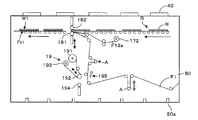
도 3은 제조 시스템을 설명하기 위한 도면.
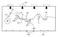
도 4는 제조 시스템의 장치 구성에 대하여 설명하기 위한 도면.
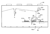
도 5a는 제조 시스템의 장치 구성에 대하여 설명하기 위한 도면.
도 5b는 제조 시스템의 장치 구성에 대하여 설명하기 위한 도면.
도 5c는 제조 시스템의 장치 구성에 대하여 설명하기 위한 도면.
도 6은 제조 시스템의 장치 구성에 대하여 설명하기 위한 도면.
도 7은 제조 시스템의 장치 구성에 대하여 설명하기 위한 도면.
도 8은 제조 시스템의 장치 구성에 대하여 설명하기 위한 도면.
도 9는 제조 시스템의 장치 구성에 대하여 설명하기 위한 도면.
도 10a는 제조 시스템의 장치 구성에 대하여 설명하기 위한 도면.
도 10b는 제조 시스템의 장치 구성에 대하여 설명하기 위한 도면.
도 10c는 제조 시스템의 장치 구성에 대하여 설명하기 위한 도면.
도 11은 제조 시스템의 장치 구성에 대하여 설명하기 위한 도면.
도 12a는 제조 시스템의 장치 구성에 대하여 설명하기 위한 도면.
도 12b는 제조 시스템의 장치 구성에 대하여 설명하기 위한 도면.
도 12c는 제조 시스템의 장치 구성에 대하여 설명하기 위한 도면.
도 13은 다른 제조 시스템의 장치 구성에 대하여 설명하기 위한 도면.
도 14a는 다른 제조 시스템의 장치 구성에 대하여 설명하기 위한 도면.
도 14b는 다른 제조 시스템의 장치 구성에 대하여 설명하기 위한 도면.
도 14c는 다른 제조 시스템의 장치 구성에 대하여 설명하기 위한 도면.1 is a flowchart of a manufacturing method of an optical display device;
2 is a diagram illustrating an example of a laminated structure of an optical member, a laminated optical member, and an optical display unit.
3 is a view for explaining a manufacturing system.
4 is a diagram for explaining an apparatus configuration of a manufacturing system.
5A is a diagram for explaining an apparatus configuration of a manufacturing system.
5B is a diagram for explaining an apparatus configuration of a manufacturing system.
5C is a diagram for explaining an apparatus configuration of a manufacturing system.
6 is a diagram for explaining an apparatus configuration of a manufacturing system.
7 is a diagram for explaining an apparatus configuration of a manufacturing system.
8 is a diagram for explaining an apparatus configuration of a manufacturing system.
9 is a diagram for explaining an apparatus configuration of a manufacturing system.
It is a figure for demonstrating the apparatus structure of a manufacturing system.
It is a figure for demonstrating the apparatus structure of a manufacturing system.
It is a figure for demonstrating the apparatus structure of a manufacturing system.
The figure for demonstrating the apparatus structure of a manufacturing system.
It is a figure for demonstrating the apparatus structure of a manufacturing system.
It is a figure for demonstrating the apparatus structure of a manufacturing system.
It is a figure for demonstrating the apparatus structure of a manufacturing system.
It is a figure for demonstrating the apparatus structure of another manufacturing system.
It is a figure for demonstrating the apparatus structure of another manufacturing system.
14B is an explanatory diagram illustrating the device configuration of another manufacturing system.
It is a figure for demonstrating the apparatus structure of another manufacturing system.
(제1 실시 형태) (1st embodiment)
본 발명의 제1 실시 형태에 대하여 이하에 설명한다. 도 1에 광학 표시 장치의 제조 방법의 일례의 흐름도를 나타낸다. 도 2에 제1, 제2 적층 광학 제품(F1, F2), 제1, 제2 광학 부재(F11, F22), 액정 셀(W)(광학 표시 유닛) 단면 구성의 모식도를 도시한다. 도 3에 도 1의 제1 실시 형태에 있어서의 광학 표시 장치의 제조 시스템의 평면 배치도의 일례를 나타낸다. 도 4 내지 도 10c는 제1 실시 형태에 있어서의 광학 표시 장치의 제조 시스템의 일례에 대하여 설명하기 위한 도면이다. 이 제1 실시 형태는 광학 부재를 광학 표시 유닛에 접합하는 위치에서, 결점이 포함되어 있다고 판정된 광학 부재를 배제하는 구성이어도 되고, 당해 접합 위치의 상류측에서 배제하는 구성이어도 된다. 또한, 결점이 포함된다고 판정된 광학 부재를 배제하는 경우에 한정되지 않고, 예를 들어 공정 검사의 샘플링, 품질 검사의 샘플링 등을 하기 위해 배제하는 경우도 예시된다.EMBODIMENT OF THE INVENTION The 1st Embodiment of this invention is described below. The flowchart of an example of the manufacturing method of an optical display apparatus is shown in FIG. The schematic diagram of the cross-sectional structure of 1st, 2nd laminated optical product F1, F2, 1st, 2nd optical member F11, F22, and liquid crystal cell W (optical display unit) is shown in FIG. FIG. 3 shows an example of a planar layout view of the manufacturing system of the optical display device in the first embodiment of FIG. 1. 4-10C is a figure for demonstrating an example of the manufacturing system of the optical display apparatus in 1st Embodiment. This 1st Embodiment may be a structure which excludes the optical member judged that the fault was included in the position which bonds an optical member to an optical display unit, and may be a structure which removes in the upstream of the said bonding position. Moreover, it is not limited to the case where the optical member judged to contain a fault is excluded, and the case where it excludes for sampling of a process inspection, sampling of a quality inspection, etc. is also illustrated, for example.
(광학 부재 및 적층 광학 제품) (Optical member and laminated optical product)
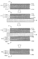
광학 표시 유닛에 접합되는 광학 부재는 편광자 필름, 위상차 필름, 시각 보상 필름, 휘도 향상 필름 등, 또는 그들 필름의 2종 이상의 조합 적층 필름이 예시된다. 이들 광학 부재의 한쪽 표면 또는 양 표면에는 보호용 투명 필름이 적층되는 경우가 있다. 이하에 있어서 제1 적층 광학 제품(F1)의 구성에 대하여 설명하지만, 제2 적층 광학 제품(F2)도 마찬가지의 구성이다. 또한, 제1 적층 광학 제품(F1)의 구성과 제2 적층 광학 제품(F2)의 구성은 달라도 된다.Examples of the optical member bonded to the optical display unit include a polarizer film, a retardation film, a vision compensation film, a brightness enhancement film, and the like, or a combination laminated film of two or more of these films. The protective transparent film may be laminated | stacked on one surface or both surfaces of these optical members. Although the structure of the 1st laminated optical product F1 is demonstrated below, the 2nd laminated optical product F2 is also the same structure. In addition, the structure of 1st laminated optical product F1 may differ from the structure of 2nd laminated optical product F2.
도 2에 도시하는 바와 같이, 제1 적층 광학 제품(F1)은 제1 광학 부재(F11)와, 이형 필름(F12)과, 표면 보호 부재(F13)를 갖는 적층 구성이다. 제1 광학 부재(F11)는 제1 편광자(F11a)와, 그 한쪽면에 접착제층(도시하지 않음)을 개재한 제1 편광자 보호 필름(F11b)과, 그 다른 쪽면에 접착제층(도시하지 않음)을 개재한 제2 편광자 보호 필름(F11c)으로 구성되어 있다. 또한, 이하에 있어서, 편광자와 편광자 보호 필름의 적층 구조를 편광판이라 칭하는 경우가 있다.As shown in FIG. 2, the 1st laminated optical product F1 is a laminated structure which has the 1st optical member F11, the release film F12, and the surface protection member F13. The first optical member F11 includes a first polarizer F11a, a first polarizer protective film F11b having an adhesive layer (not shown) on one side thereof, and an adhesive layer (not shown) on the other side thereof. It is comprised by the 2nd polarizer protective film F11c through (). In addition, below, the laminated structure of a polarizer and a polarizer protective film may be called a polarizing plate.
제1, 제2 편광자 보호 필름(F11b, F11c)은, 예를 들어 트리아세틸셀룰로오스(TAC) 필름, 폴리에틸렌테레프탈레이트(PET) 필름을 들 수 있다. 또한, 표면 보호 부재(F13)는 제1 편광자 보호 필름(F11b)과 약점착제층(F15)을 통해 설치되어 있다. 또한, 이형 필름(F12)은 제2 편광자 보호 필름(F11c)과 점착제층(F14)을 통해 설치되어 있다. 제1, 제2 편광자 보호 필름(F11b, F11c)은 특별히 한정되지 않고, 예를 들어 투명성, 기계적 강도, 열안정성, 수분 차단성, 등방성 등이 우수한 열가소성 수지를 재료로 하는 필름으로 구성된다. 이러한 열가소성 수지의 구체예로서는, 트리아세틸셀룰로오스 등의 셀룰로오스 수지, 폴리에스테르 수지, 폴리에테르술폰 수지, 폴리술폰 수지, 폴리카르보네이트 수지, 폴리아미드 수지, 폴리이미드 수지, 폴리올레핀 수지, (메트)아크릴 수지, 환상 폴리올레핀 수지(노르보르넨계 수지), 폴리아릴레이트 수지, 폴리스티렌 수지, 폴리비닐알코올 수지, 및 이들의 혼합물을 들 수 있다.Examples of the first and second polarizer protective films F11b and F11c include triacetyl cellulose (TAC) films and polyethylene terephthalate (PET) films. In addition, surface protection member F13 is provided through 1st polarizer protective film F11b and weak adhesive layer F15. In addition, the release film F12 is provided through the 2nd polarizer protective film F11c and the adhesive layer F14. The 1st, 2nd polarizer protective films F11b and F11c are not specifically limited, For example, it is comprised from the film which uses thermoplastic resin excellent in transparency, mechanical strength, thermal stability, moisture barrier property, isotropy, etc. Specific examples of such thermoplastic resins include cellulose resins such as triacetyl cellulose, polyester resins, polyether sulfone resins, polysulfone resins, polycarbonate resins, polyamide resins, polyimide resins, polyolefin resins, and (meth) acrylic resins. , Cyclic polyolefin resin (norbornene-based resin), polyarylate resin, polystyrene resin, polyvinyl alcohol resin, and mixtures thereof.
또한, 제1 광학 부재(F11)는 실용시에 각종 광학층을 적층한 다층 적층 구조의 광학 필름을 예시할 수 있다. 그 광학층에 대해서는 특별히 한정되는 것은 아니지만, 예를 들어 편광자 보호 필름의 편광자를 접착시키지 않는 면(접착제 도포층을 형성하지 않는 면)에 대하여, 하드 코트 처리나 반사 방지 처리, 스티킹 방지나, 확산 또는 안티글레어를 목적으로 한 표면 처리를 실시하거나, 시각 보상 등을 목적으로 한 배향 액정층을 적층하는 방법을 들 수 있다. 또한, 반사판이나 반투과판, 위상차판[1/2이나 1/4 등의 파장판(λ판)을 포함함], 시각 보상 필름 등의 액정 표시 장치 등의 형성에 사용되는 광학 필름을 1층 또는 2층 이상 접합한 것도 예로 들 수 있다.In addition, the 1st optical member F11 can illustrate the optical film of the multilayer laminated structure which laminated | stacked various optical layers at the time of practical use. Although it does not specifically limit about the optical layer, For example, with respect to the surface which does not adhere the polarizer of a polarizer protective film (surface which does not form an adhesive application layer), a hard-coat process, an antireflection process, sticking prevention, And a method of performing surface treatment for the purpose of diffusion or antiglare, or laminating an alignment liquid crystal layer for the purpose of visual compensation or the like. Moreover, one layer of optical film used for formation of liquid crystal display devices, such as a reflecting plate, a semi-transmissive plate, a retardation plate (including wavelength plates (lambda plate), such as 1/2 or 1/4), and a visual compensation film, etc. Or what joined two or more layers is mentioned, for example.
제1 편광자(F11a)는, 예를 들어 폴리비닐알코올계 필름에 의해 구성된다.The first polarizer F11a is made of, for example, a polyvinyl alcohol film.
이형 필름(F12)은 제1 점착제층(F14)의 노출면에 대하여, 그 오염 방지 등을 목적으로 임시 부착되어 있다. 이에 의해, 통례의 취급 상태로 점착제층(F14)에 접촉하는 것을 방지할 수 있다. 이형 필름(F12)으로서는, 예를 들어 플라스틱 필름, 고무 시트, 종이, 천, 부직포, 네트, 발포 시트나 금속박, 그들의 라미네이트체 등의 적절한 박엽체를, 필요에 따라서 실리콘계나 장쇄 알킬계, 불소계나 황화몰리브덴 등이 적절한 박리제로 코트 처리한 것 등의, 종래에 준한 적절한 것을 사용할 수 있다.The release film F12 is temporarily attached to the exposed surface of the 1st adhesive layer F14 in order to prevent the contamination. Thereby, contact with adhesive layer F14 can be prevented in a usual handling state. As the release film (F12), suitable thin films such as plastic films, rubber sheets, paper, cloth, nonwoven fabrics, nets, foam sheets, metal foils, and laminates thereof may be, for example, silicone type, long chain alkyl type, fluorine type, or the like. Suitable ones according to the prior art, such as molybdenum sulfide etc. which were coat-treated with a suitable release agent, can be used.
표면 보호 부재(F13)는 약점착제층(F15)을 통해 형성된다. 그 목적은, 흠집 방지, 오염 방지 등이 주 목적이다. 표면 보호 부재로서는, 예를 들어 플라스틱 필름, 고무 시트, 종이, 천, 부직포, 네트, 발포 시트나 금속박, 그들의 라미네이트체 등의 적절한 박엽체를, 필요에 따라서 실리콘계나 장쇄 알킬계, 불소계나 황화몰리브덴 등이 적절한 박리제로 코트 처리한 것 등의, 종래에 준한 적절한 것을 사용할 수 있다.Surface protection member F13 is formed through weak adhesive layer F15. The main purpose is to prevent scratches, to prevent contamination. As a surface protection member, suitable thin bodies, such as a plastic film, a rubber sheet, paper, a cloth, a nonwoven fabric, a net, a foam sheet, a metal foil, and those laminates, are silicone type | system | group, long-chain alkyl type, fluorine type, and molybdenum sulfide as needed, for example. The appropriate thing according to the past, such as what coat-treated with the appropriate peeling agent, etc. can be used.
점착제층(F14), 약점착제층(F15)은 액정 셀 등의 다른 부재와 접착하기 위해 형성되어 있다. 점착제층(F14), 약점착제층(F15)을 구성하는 점착제로서는, 특별히 한정되는 것은 아니지만, 아크릴계 등의 종래에 준한 적절한 점착제로 각각 형성할 수 있다.The adhesive layer F14 and the weak adhesive layer F15 are formed in order to adhere | attach with other members, such as a liquid crystal cell. Although it does not specifically limit as an adhesive which comprises the adhesive layer F14 and the weak adhesive layer F15, It can form each with the appropriate adhesive according to the prior art, such as an acryl type.
(광학 표시 장치의 제조 방법 및 그 제조 시스템) (Manufacturing method of optical display device and manufacturing system thereof)
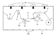
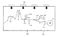
이하의 각 공정 및 각 장치 처리 동작은 공장 내로부터 격리된 격리 구조(50) 내에 있어서 행해진다. 격리 구조(50)는 투명 재료의 벽과 골조 구조로 구성된다. 격리 구조(50)의 천장에는 송풍 장치(40)가 설치된다. 송풍 장치(40)는 HEPA 필터를 구비하고, 청정도가 높은 공기를 격벽 구조(50) 내부에 송풍하여 청정 공기의 기류를 발생시킨다. 격벽 구조(50)의 벽면 하부에는 내부 공기를 외부로 배출시키기 위한 공기 배출 개구부(50a)가 형성되어 있다. 또한, 외부로부터의 침입물을 방지하기 위해 개구면에는 필터를 설치할 수도 있다. 이 격벽 구조(50), 송풍 장치(40)에 의해 제조 시스템 전체를 청정 환경으로 유지할 수 있고, 외부로부터의 이물질 혼입을 적절하게 방지할 수 있다. 또한, 제조 시스템만을 격벽 구조(50)로 외부로부터 격리하고 있기 때문에, 공장 전체를 소위 클린룸으로 할 필요가 없다.Each process and each apparatus treatment operation described below are performed in an
(제조 흐름) (Production flow)
(1) 제1 롤 원재료 준비 공정(S1). 긴 제1 적층 광학 제품(F1)을 제1 롤 원재료로서 준비한다. 제1 롤 원재료의 폭은 광학 표시 유닛의 접합 크기에 의존하고 있다.(1) First roll raw material preparation step (S1). The long first laminated optical product F1 is prepared as a first roll raw material. The width of the first roll raw material depends on the bonding size of the optical display unit.
(2) 반송 공정(S2). 준비되어 설치된 제1 롤 원재료로부터 제1 적층 광학 제품(F1)을 풀어내어, 하류측으로 반송한다. 제1 적층 광학 제품(F1)을 반송하는 제1 반송 장치(12)는, 예를 들어 닙 롤러쌍, 텐션 롤러, 회전 구동 장치, 어큐뮬레이트 장치(A), 센서 장치, 제어 장치 등으로 구성되어 있다(도 4 참조).(2) conveyance process (S2). The first laminated optical product F1 is removed from the prepared first roll raw material and conveyed to the downstream side. The
(3) 이형 필름 제거 공정(S3). 도 4에 도시하는 제1 검사 전 박리 장치(13)는 반송되고 있는 제1 적층 광학 제품(F1)으로부터 이형 필름(F12)을 박리한다. 제1 검사 전 박리 장치(13)는 박리 기구(131)의 나이프 에지부로, 반송되어 온 제1 적층 광학 제품(F1)으로부터 이형 필름(F12)을 감아 걸어 박리하고, 이 박리된 이형 필름(F12)을 롤(132)에 권취하는 구성이다.(3) Release film removal process (S3). The 1st
(4) 결점 검사 공정(S4). 도 4에 도시하는 제1 결점 검사 장치(14)는 이형 필름 제거 공정(S3) 후에, 제1 적층 광학 제품(F1)의 결점을 검사한다. 이형 필름(F12)에 내재하는 위상차를 고려할 필요 없이, 제1 광학 부재(F11)의 결점 검사를 행할 수 있다. 여기서의 결점 검사 방법으로서는, 제1 적층 광학 제품(F1)의 양면에 대하여, 투과광, 반사광에 의한 화상 촬영ㆍ화상 처리하는 방법, 검사용 편광 필름을 CCD 카메라와 검사 대상물 사이에, 검사 대상인 편광판의 편광축과 크로스니콜이 되도록 배치(0도 크로스라 칭하는 경우가 있음)하여 화상 촬영ㆍ화상 처리하는 방법, 검사용 편광 필름을 CCD 카메라와 검사 대상물 사이에, 검사 대상인 편광판의 편광축과 소정 각도(예를 들어, 0도보다 크고 10도 이내의 범위)가 되도록 배치(x도 크로스라 칭하는 경우가 있음)하여 화상 촬영ㆍ화상 처리하는 방법을 예로 들 수 있다.(4) Defect inspection step (S4). The 1st
제1 결점 검사 장치(14)에서 얻어진 결점의 정보는, 그 위치 정보(예를 들어, 위치 좌표)와 함께 결부되어 제어 장치에 송신되고, 후술하는 제1 절단 장치(16)에 의한 절단 방법에 기여시킬 수 있다.The defect information obtained by the 1st
결점을 포함하는 제1 적층 광학 제품(F1)은, 후술하는 제1 배제 장치(19)에 의해 배제되어, 광학 표시 유닛(W)에는 부착되지 않도록 구성된다.The 1st laminated optical article F1 containing a fault is excluded by the
(5) 이형 필름 접합 공정(S5). 도 4에 도시하는 제1 이형 필름 접합 장치(15)는 결점 검사 공정(S4) 후에, 이형 필름(F12a)을 제1 점착제층(F14)을 통해 제1 광학 부재(F11)에 접합한다.(5) Release film bonding process (S5). The 1st release film bonding apparatus 15 shown in FIG. 4 bonds release film F12a to 1st optical member F11 via 1st adhesive layer F14 after a defect inspection process S4.
제1 이형 필름 접합 장치(15)는 결점 검사 공정(S4) 후에, 이형 필름(F12a)을 제1 점착제층(F14)을 통해 제1 광학 부재(F11)에 접합한다. 도 4에 도시한 바와 같이, 이형 필름(F12a)의 롤 원재료(151)로부터 이형 필름(F12a)을 풀어내고, 하나 또는 복수의 롤러쌍(152)으로 이형 필름(F12a)과 제1 적층 광학 제품(F1)을 협지하여, 당해 롤러쌍(152)으로 소정의 압력을 작용시켜, 이형 필름(F12a)을 제1 점착제층(F14)을 통해 제1 광학 부재(F11)에 접합한다.The 1st release film bonding apparatus 15 bonds the release film F12a to the 1st optical member F11 via the 1st adhesive layer F14 after a defect inspection process S4. As shown in FIG. 4, the release film F12a is released from the roll
(6) 절단 공정(S6). 계속해서, 이형 필름 접합 공정(S5) 후에, 도 4에 도시하는 제1 절단 장치(16)는 이형 필름(12a)을 남기고, 표면 보호 부재(13), 약점착제층(15), 제1 광학 부재(11) 및 제1 점착제층(F14)을 절단한다. 제1 결점 검사 처리에서 검출된 결점의 위치 좌표에 기초하여, 제1 절단 장치(16)는 결점 부분을 피하도록 소정 크기로 절단하는 것이 바람직하다. 절단 방법으로서는, 예를 들어 레이저 절단, 커터 절단, 그 밖의 공지의 절단 방법을 들 수 있다. 제1 결점 검사 장치(14)에서 얻어진 결점의 정보에 기초하여, 결점을 피하도록 절단하도록 구성된다. 이에 의해, 제1 적층 광학 제품(F1)의 수율이 대폭 향상된다. 결점을 포함하는 제1 적층 광학 제품(F1)은, 후술하는 제1 배제 장치(19)에 의해 배제되어 광학 표시 유닛(W)에는 부착되지 않도록 구성된다.(6) Cutting process (S6). Subsequently, after the release film bonding step (S5), the
(7) 양품 판정(도 1, S7). 제1 결점 검사 장치(14)에 의한 결점 검사의 결과, 양품인지 여부가 판정된다. 양품 판정의 판정 기준은 미리 설정되고, 예를 들어 소정 면적당의 결점수, 결점 크기, 결점의 종류에 의해 설정된다. 고정밀도의 표시 성능이 요구될수록, 양품 판정은 엄격한 것으로 된다.(7) Good quality judgment (FIG. 1, S7). As a result of the defect inspection by the 1st
(7-1) 배제 공정(도 1, S7-1). 결점 검사에서 양품 판정된 제1 광학 부재(F11)의 배제 처리가 행해진다(도 5a 내지 도 5c). 배제 처리의 구성예는 후술한다.(7-1) Exclusion process (FIG. 1, S7-1). Exclusion processing of the first optical member F11 determined as good in the defect inspection is performed (FIGS. 5A to 5C). The structural example of an exclusion process is mentioned later.
(8) 접합 공정(S8). 배제에 관련된 광학 부재가 아니면 접합 처리가 행해진다. 제1 박리 장치(17)에 의해 이형 필름(F12a)을 박리하면서, 제1 접합 장치(18)에 의해 이형 필름(F12a)이 박리된 제1 광학 부재(F11)를 제1 점착제층(F14)을 통해 광학 표시 유닛(W)에 접합한다(도 5a 참조).(8) Bonding process (S8). If it is not the optical member which concerns on removal, the bonding process is performed. While peeling off the release film F12a by the 1st peeling apparatus 17, the 1st adhesive layer F14 made the 1st optical member F11 with which the release film F12a was peeled off by the 1st bonding apparatus 18. FIG. It bonds to the optical display unit W via (FIG. 5A).
제1 박리 장치의 박리 기구(171)로서는, 선단이 뾰족한 나이프 에지부를 갖고, 이 나이프 에지부에 이형 필름(F12a)을 감아 걸어 반전 이송함으로써, 이형 필름(F12a)을 박리함과 함께, 이형 필름(F12a)을 박리한 후의 제1 적층 광학 제품(F1)을 광학 표시 유닛(W)면에 송출하도록 구성된다. 박리된 이형 필름(F12a)은 롤(172)에 권취된다.As the
도 5a에 도시한 바와 같이, 접합 처리의 경우에, 누름 롤러(181)를 표면 보호 부재(F13)면에 접촉하고, 광학 표시 유닛(W)의 하면을 안내 롤러(182)로 접촉하여, 제1 적층 광학 제품(F1)을 광학 표시 유닛(W)면에 가압하여, 이형 필름(F12a)이 박리되어 노출된 제1 광학 부재(F11)의 접합면[제1 점착제층(F14)의 면]을 광학 표시 유닛(W)면에 접합한다. 누름 롤러(181) 및 안내 롤러(182)는 탄성 롤러(예를 들어, 실리콘 고무제)이어도 되고, 금속제 롤러이어도 된다.As shown in FIG. 5A, in the case of the bonding process, the
(9) 광학 표시 유닛의 세정 공정(S9). 광학 표시 유닛(W)은 연마 세정 장치 및 물 세정 장치에 의해 그 표면이 미리 세정된다. 세정된 광학 표시 유닛(W)은 반송 수단(R)에 의해 제1 접합 장치까지 반송된다. 반송 수단(R)은, 예를 들어 복수의 반송 굴림대, 반송 방향 전환 기구, 회전 구동 장치, 센서 장치, 제어 장치 등으로 구성된다.(9) Cleaning process of optical display unit (S9). The surface of the optical display unit W is cleaned in advance by an abrasive cleaning device and a water cleaning device. The washed optical display unit W is conveyed by the conveyance means R to a 1st bonding apparatus. The conveying means R is comprised, for example with a some conveyance roller, a conveying direction switching mechanism, a rotation drive apparatus, a sensor apparatus, a control apparatus, etc.
이상의 공정에 의해, 광학 표시 유닛(W)의 한쪽면에 제1 광학 부재(F11)가 접합된다. 이하에서는, 그 다른 면에 제2 광학 부재(F21)를 접합하는 제조 공정에 대하여 도 9, 도 10a 내지 도 10c를 이용하여 설명한다. 또한, 상술한 제조 공정과 같은 공정에 대해서는 간단하게 설명하는 경우가 있다.By the above process, the 1st optical member F11 is bonded by one surface of the optical display unit W. As shown in FIG. Hereinafter, the manufacturing process of bonding the 2nd optical member F21 to the other surface is demonstrated using FIG. 9, FIG. 10A-FIG. 10C. In addition, the process similar to the manufacturing process mentioned above may be demonstrated briefly.
(10) 제2 롤 원재료 준비 공정(S10). 긴 제2 적층 광학 제품(F2)을 제2 롤 원재료로서 준비한다. 제2 적층 광학 제품(F2)의 적층 구조는 도 2에 도시하는 구성이다. 제2 적층 광학 제품(F2)은 제2 광학 부재(F21)와, 이형 필름(F22)과, 표면 보호 부재(F23)를 갖는다. 제2 광학 부재(F21)는 제2 편광자(F21a)와, 그 한쪽면에 접착제층(도시하지 않음)을 개재한 제3 편광자 보호 필름(F21b)과, 그 다른 쪽면에 접착제층(도시하지 않음)을 개재한 제4 편광자 보호 필름(F21c)으로 구성되어 있다.(10) 2nd roll raw material preparation process (S10). The long second laminated optical product F2 is prepared as a second roll raw material. The laminated structure of the 2nd laminated optical product F2 is the structure shown in FIG. The second laminated optical product F2 has a second optical member F21, a release film F22, and a surface protective member F23. The second optical member F21 includes a second polarizer F21a, a third polarizer protective film F21b having an adhesive layer (not shown) on one side thereof, and an adhesive layer (not shown) on the other side thereof. It is comprised by the 4th polarizer protective film F21c through ().
(11) 반송 공정(S11). 준비되어 설치된 제2 롤 원재료로부터 제2 적층 광학 제품(F2)을 풀어내어, 하류측으로 반송한다. 도 9에 도시하는, 제2 적층 광학 제품(F2)을 반송하는 제2 반송 장치(22)는 제1 반송 장치(12)와 마찬가지의 구성을 갖고 있지만, 제2 적층 광학 제품(F2)의 반송 방향은 제1 적층 광학 제품(F1)의 반송 방향과 반대이며, 또한 이형 필름(F22)면을 상방을 향하여 반송시키는 구성이다.(11) conveyance process (S11). The second laminated optical product F2 is removed from the prepared second roll raw material and conveyed to the downstream side. Although the 2nd conveying
(12) 이형 필름 제거 공정(S12). 도 9에 도시하는 제2 검사 전 박리 장치는 반송되고 있는 제2 적층 광학 제품(F2)으로부터 이형 필름(F22)을 박리한다. 박리 기구는 상술한 박리 기구와 마찬가지이며, 제2 검사 전 박리 장치는 박리 기구(231)의 나이프 에지부에 이형 필름(F22)을 감아 걸어 박리하고, 이 박리된 이형 필름(F22)을 롤(232)에 권취하는 구성이다.(12) Release film removal process (S12). The peeling apparatus before the 2nd inspection shown in FIG. 9 peels the release film F22 from the 2nd laminated optical product F2 conveyed. The peeling mechanism is the same as the peeling mechanism described above, and the peeling device before the second inspection wound the release film F22 around the knife edge portion of the
(13) 결점 검사 공정(S13). 도 9에 도시하는 제2 결점 검사 장치(24)는 이형 필름 제거 공정(S11) 후에, 제2 적층 광학 제품(F2)의 결점을 검사한다. 제2 결점 검사 장치(24)의 구성은, 상술한 제1 결점 검사 장치(14)의 구성과 마찬가지이다.(13) Defect inspection step (S13). The 2nd
(14) 이형 필름 접합 공정(S14). 도 9에 도시하는 제2 이형 필름 접합 장치(25)는 제2 결점 검사 공정(S12) 후에, 이형 필름(F22a)을, 제2 점착제층(F24)을 통해 제2 광학 부재(F21)에 접합한다. 제2 이형 필름 접합 장치(25)는, 도 4에 도시한 바와 같이, 이형 필름(F22a)의 롤 원재료(251)로부터 이형 필름(F22a)을 풀어내고, 하나 또는 복수의 롤러쌍(252)으로 이형 필름(F22a)과 제2 적층 광학 제품(F2)을 협지하여, 이형 필름(F22a)을 제2 점착제층(F24)을 통해 제2 광학 부재(F21)에 접합한다.(14) Release film bonding process (S14). In the second release film bonding apparatus 25 illustrated in FIG. 9, the release film F22a is bonded to the second optical member F21 through the second pressure sensitive adhesive layer F24 after the second defect inspection step S12. do. As shown in FIG. 4, the second release film bonding apparatus 25 releases the release film F22a from the roll
(15) 절단 공정(S15). 이형 필름 접합 공정(S14) 후에, 도 9에 도시하는 제2 절단 장치(26)는 이형 필름(22a)을 남기고, 표면 보호 부재(F23), 약점착제층(F25), 제2 광학 부재(F21) 및 제2 점착제층(F24)을 절단한다. 제2 절단 장치(26)는 상술한 제1 절단 장치(16)와 마찬가지의 구성이다.(15) Cutting process (S15). After the release film bonding step S14, the
(16) 양품 판정(S16). 제2 결점 검사 장치(24)에 의한 결점 검사의 결과, 양품인지 여부가 판정된다. 양품 판정의 판정 기준은 미리 설정되고, 예를 들어 소정 면적당의 결점수, 결점 크기, 결점의 종류에 의해 설정된다. 고정밀도의 표시 성능이 요구될수록, 양품 판정은 엄격한 것으로 된다.(16) Good judgment (S16). As a result of the defect inspection by the 2nd
(16-1) 제2 광학 필름 배제 공정(S16-2). 결점 검사에서 양품 판정된 제2 광학 부재(F21)의 배제 처리가 행해진다. 배제 처리의 구성예는 후술한다.(16-1) 2nd optical film removal process (S16-2). The exclusion process of the 2nd optical member F21 judged good quality by the fault inspection is performed. The structural example of an exclusion process is mentioned later.
(17) 접합 공정(S17). 결점 검사에서 양품 판정된 제2 광학 부재의 접합 처리가 행해진다. 도 10a에 도시한 바와 같이, 제2 박리 장치(27)를 사용하여 제2 이형 필름(F22)을 제거하면서(박리 공정), 제2 접합 장치(28)를 사용하여 당해 제2 이형 필름(F22)이 제거된 제2 광학 부재(F21)를, 제2 점착제층(F24)을 통해 광학 표시 유닛(W1)에 접합한다. 또한, 제2 광학 부재(F21)를 광학 표시 유닛(W1)에 접합하기 전에, 반송 기구(R)의 반송 방향 전환 기구에 의해 광학 표시 유닛(W1)을 90도 회전시켜, 제1 광학 부재(F11)의 편광자와 제2 광학 부재(F21)의 편광자를 크로스니콜의 관계로 하는 경우가 있다.(17) Bonding step (S17). The bonding process of the 2nd optical member whose quality was determined by defect inspection is performed. As shown in FIG. 10A, while removing the 2nd release film F22 using the 2nd peeling apparatus 27 (peeling process), the 2nd release film F22 using the
제2 박리 장치의 박리 기구(271)로서는, 선단이 날카로운 나이프 에지부를 갖고, 이 나이프 에지부에 이형 필름(F22a)을 감아 걸어 반전 이송함으로써, 이형 필름(F22a)을 박리함과 함께, 이형 필름(F22a)을 박리한 후의 제2 적층 광학 제품(F2)을 광학 표시 유닛(W1)면에 송출하도록 구성된다. 박리된 이형 필름(F22a)은 롤(272)에 권취된다.As the
도 10a에 도시한 바와 같이, 접합 처리의 경우에, 누름 롤러(281)를 표면 보호 부재(F23)면에 접촉하고, 광학 표시 유닛(W1)의 상면을 안내 롤러(282)로 접촉하여, 제2 적층 광학 제품(F2)을 광학 표시 유닛(W1)면에 가압하여, 이형 필름이 박리되어 노출된 제2 광학 부재(F21)의 접합면[제2 점착제층(F24)의 면]을 광학 표시 유닛(W1)면에 접합한다.As shown in Fig. 10A, in the case of the bonding process, the
광학 표시 장치(W12)의 검사 공정. 검사 장치(30)는 광학 부재가 양면에 부착된 광학 표시 장치(W12)를 검사한다. 검사 방법으로서는, 광학 표시 장치(W12)의 양면에 대하여, 반사광에 의한 화상 촬영ㆍ화상 처리하는 방법이 예시된다. 또한 다른 방법으로서, 검사용 편광 필름을 CCD 카메라와 검사 대상물 사이에 설치하는 방법도 예시된다. 또한, 화상 처리의 알고리즘은 공지의 방법을 적용할 수 있고, 예를 들어 2치화 처리에 의한 농담 판정에 의해 결점을 검출할 수 있다.Inspection process of the optical display device W12. The inspection apparatus 30 inspects the optical display device W12 having the optical members attached to both surfaces. As the inspection method, a method of image capturing and image processing by reflected light is exemplified for both surfaces of the optical display device W12. Moreover, as another method, the method of providing an inspection polarizing film between a CCD camera and an inspection object is also illustrated. In addition, the algorithm of an image process can apply a well-known method, for example, can detect a fault by the light and shade determination by a binarization process.
검사 장치(30)에서 얻어진 결점의 정보에 기초하여, 광학 표시 장치(W12)의 양품 판정이 이루어진다. 양품 판정된 광학 표시 장치(W12)는 다음 실장 공정으로 반송된다. 불량품 판정된 경우, 리워크 처리가 실시되어, 새롭게 광학 필름이 부착되고, 계속해서 검사되어, 양품 판정의 경우, 실장 공정으로 이행하고, 불량품 판정의 경우, 다시 리워크 처리로 이행하거나 혹은 폐기 처분된다.On the basis of the defect information obtained by the inspection apparatus 30, the quality judgment of the optical display device W12 is made. The quality-determined optical display device W12 is conveyed to the next mounting process. In the case of a defective product determination, a rework process is performed, and an optical film is newly attached and subsequently inspected, and in the case of a good product determination, the process proceeds to a mounting process, and in the case of a defective product determination, the process is reworked or discarded. do.
이상의 일련의 제조 공정에 있어서, 제1 광학 부재(F11)의 접합 공정과 제2 광학 부재(F21)의 접합 공정을 연속된 제조 라인으로 실행함으로써, 광학 표시 장치를 적절하게 제조할 수 있다. 특히, 상기 각 공정을 공장 내로부터 격리한 격리 구조 내부에서 행함으로써, 청정도가 확보된 환경에서 광학 부재를 광학 표시 유닛에 접합할 수 있고, 고품질의 광학 표시 장치를 제조할 수 있다.In the above series of manufacturing processes, the optical display device can be appropriately manufactured by performing the bonding process of the first optical member F11 and the bonding process of the second optical member F21 in a continuous production line. In particular, by performing the above steps inside an isolation structure isolated from the factory, the optical member can be bonded to the optical display unit in an environment where cleanliness is ensured, and a high quality optical display device can be manufactured.
(배제 장치) (Exclusion device)
도 5a 내지 도 5c 및 도 7 내지 도 9는 배제 장치의 구성예에 대하여 설명하기 위한 도면이다. 제1 배제 장치(19)의 구성은, 여기서 예시하는 구성에 제한되지 않고, 이들 구성의 각종 변형예도 적용할 수 있고, 이 변형예는 본 발명의 기술적 사상의 범위에 포함된다.5A to 5C and 7 to 9 are diagrams for explaining a configuration example of the exclusion apparatus. The structure of the
(배제 장치의 실시예 1) (Example 1 of an exclusion apparatus)
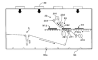
제1 적층 광학 제품(F1)을 배제하는 제1 배제 장치(19)에 대하여 설명한다. 도 5a에 도시하는 제1 배제 장치(19)의 동작을 도 6을 이용하여 설명한다. 이 실시예 1의 제1 배제 장치(19)는 광학 표시 유닛(W)과 광학 부재(F11)의 접합 위치에서, 배제에 관련된 광학 부재(F11)를 배제하는 구성이다. 배제용 롤러(192)는 탄성 롤러(예를 들어, 실리콘 고무제)이어도 되고, 금속제 롤러이어도 된다.The
(1) 배제에 관련된 광학 부재(F11)가 접합 위치로 반송되어 오면, 광학 표시 유닛(W)의 반송이 정지한다[반송 기구(R)에 어큐뮬레이트 기구가 구비되어 있음]. 그리고, 안내 롤러(182)는 수직 하방으로 이동한다.(1) When the optical member F11 concerning removal is conveyed to the bonding position, conveyance of the optical display unit W will stop (the accumulating mechanism is provided in the conveyance mechanism R). And the
(2) 계속해서, 테이프(191)가 걸쳐진 배제용 롤러(192)는 안내 롤러(182)의 정위치인 접합 위치로 이동한다.(2) Subsequently, the
(3) 누름 롤러(181)는 수직 하방으로 이동한다.(3) The
(4) 누름 롤러(181)는 박리 기구(171)에 의해 이형 필름(F12a)이 박리된 배제에 관련된 광학 부재(F11)의 점착제층(F14)면을 배제용 롤러(192)측으로 가압하여, 배제에 관련된 광학 부재(F11)를 테이프(191)에 부착한다. 테이프(191)와 함께 배제에 관련된 광학 부재(F11)를 권취 롤러(193)에 권취한다.(4) The
(5) 배제 후, 누름 롤러(181)는 상승하고, 배제용 롤러(192)는 원위치로 복귀하고, 안내 롤러(182)는 원위치로 복귀한다. 이상의 동작은 제어 장치(1)에 의해 제어된다.(5) After the exclusion, the
(배제 장치의 실시예 2) (Example 2 of the exclusion apparatus)
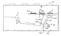
도 5b에 도시하는 실시예 2의 제1 배제 장치(19)는 광학 표시 유닛(W)과 광학 부재(F11)의 접합 위치보다 상류측에서, 배제에 관련된 광학 부재(F11)를 배제하는 구성이다. 이 구성의 경우, 광학 표시 유닛(W)과 광학 부재(F11)의 접합 처리를 장시간 중단시키는 일이 없기 때문에, 실시예 1의 구성보다도 생산성이 높다. 도 5b에 나타내는 실시예 2의 제1 배제 장치(19)의 동작을 도 7을 이용하여 설명한다.The
제1 배제 장치(19)는 제1 적층 광학 제품(F1)으로부터 이형 필름(F12a)을 박리하는 박리 기구(195)와, 테이프(191)와, 테이프(191)가 걸쳐진 배제용 롤러(192)와, 이형 필름(F12a)이 박리된 배제에 관련된 제1 광학 부재(F11)를 배제용 롤러(192)측으로 가압하는 배제용 누름 롤러(194)와, 배제에 관련된 제1 광학 부재(F11)가 부착된 테이프(191)를 권취하는 권취 롤러(193)와, 당해 장치의 하류측에 배치되는 어큐뮬레이트 장치(A)로 구성된다. 배제용 롤러(192) 및 배제용 누름 롤러(194)는 탄성 롤러(예를 들어, 실리콘 고무제)이어도 되고, 금속제 롤러이어도 된다. 그 동작은 이하와 같다.The
(1) 배제에 관련된 제1 광학 부재(F11)가 배제 위치로 반송되어 오면, 박리 기구(195)가 작동하여 배제 위치로 이동한다. 박리 기구(195)는 상기에서 설명한 나이프 에지부를 갖는 박리 기구와 마찬가지의 구성이지만, 이 박리 기구(195)는 배제 처리시에 배제 위치로 이동하는 기구를 구비하고 있다. 이동한 박리 기구(195)의 나이프 에지부 선단은 테이프(191)가 걸쳐진 배제용 롤러(192)측에 위치하고, 이형 필름(F12a)이 박리된 제1 광학 부재(F11)가 배제용 롤러(192)에 적재되는 구성이다. 또한, 어큐뮬레이트 장치(A)는 구동 상태이며, 배제 처리 중에 광학 표시 유닛(W)과 제1 광학 부재(F11)의 접합 처리가 중단되지 않도록 동작한다.(1) When the 1st optical member F11 concerning removal is conveyed to an exclusion position, the
(2) 배제용 누름 롤러(194)가 배제 위치인 접합 위치로 이동한다.(2) The
(3) 배제용 누름 롤러(194)는 배제에 관련된 제1 광학 부재(F11)의 점착제층(F14)면을 배제용 롤러(192)측으로 가압하여, 제1 광학 부재(F11)를 테이프(191)에 부착한다. 테이프(191)와 함께 제1 광학 부재(F11)를 권취 롤러(193)에 권취한다.(3) The
(4) 배제 후, 배출용 누름 롤러(194)는 상승하고, 박리 기구(195)는 원위치로 복귀한다. 이상의 동작은 제어 장치(1)에 의해 제어된다.(4) After removal, the
(배제 장치의 실시예 3) (Example 3 of an exclusion apparatus)
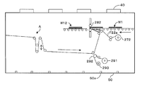
도 5c에 도시하는 실시예 3의 제1 배제 장치(19)는 광학 표시 유닛(W)과 광학 부재(F11)의 접합 위치보다 상류측에서, 배제에 관련된 광학 부재(F11)를 배제하는 구성이다. 이 구성의 경우, 광학 표시 유닛(W)과 광학 부재의 접합 처리를 장시간 중단시키는 일이 없으므로, 실시예 1의 구성보다도 생산성이 높다. 도 5c에 도시하는 실시예 3의 제1 배제 장치(19)의 동작을 도 8을 이용하여 설명한다. 제1 배제 장치(19)는 점착 테이프(191)와, 점착 테이프(191)가 걸쳐진 배제용 롤러(192)와, 점착 테이프(191)를 권취하는 권취 롤러(193)로 구성된다. 실시예 3은, 실시예 2와 같이 박리 기구(195), 누름 롤러(194), 어큐뮬레이트 장치(A)를 구비하고 있지 않기 때문에, 장치를 간단하게 구성할 수 있다. 그 동작은 이하와 같다.The
(1) 배제에 관련된 제1 광학 부재(F11)가 배제 위치로 반송되어 오면, 점착 테이프(191)가 걸쳐진 배제용 롤러(192)는 배제 위치의 롤러(121)측으로 이동한다. 배제 위치는, 예를 들어 반송 장치(12)의 롤러(121)이다.(1) When the 1st optical member F11 concerning removal is conveyed to an exclusion position, the
(2) 배제용 롤러(192)는 제1 광학 부재(F11)를 롤러(121)측으로 가압하여, 배제에 관련된 제1 광학 부재(F11)를 점착 테이프(191)에 부착한다. 그리고, 점착 테이프(191)와 함께 제1 광학 부재(F11)를 권취 롤러(193)에 권취한다.(2) The
(3) 배제 후, 배제용 롤러(192)는 원위치로 복귀한다. 이상의 배제 처리 중에 광학 표시 유닛(W)과 제1 광학 부재(F11)의 접합 처리는 중단되지 않도록 동작되고 있다. 이상의 동작은 제어 장치(1)에 의해 제어된다.(3) After removal, the
이하에 있어서, 배제에 관련된 제2 광학 부재(F21)를 배제하는 제2 배제 장치(29)에 대하여 설명한다. 도 10a에 도시하는 제2 배제 장치(29)의 구성은 상술한 도 5a의 구성과 마찬가지이며, 그 동작도 마찬가지이다. 예를 들어 결점을 포함하는 제2 광학 부재(F21)가 접합 위치로 반송되어 오면, 안내 롤러(282)가 수직 상방으로 이동한다. 계속해서, 테이프(291)가 걸쳐진 배제용 롤러(292)가 안내 롤러(282)의 정위치인 접합 위치로 이동한다. 누름 롤러(281)를 수직 상방으로 이동시키고, 결점을 포함하는 제2 광학 부재(F21)의 점착제층(F24)면을 테이프(291)에 가압하여, 제2 광학 부재(F21)를 테이프(291)에 부착하고, 테이프(291)와 함께 결점을 포함하는 제2 광학 부재(F21)를 롤러(293)에 권취한다.Below, the
또한, 도 10b에 도시하는 제2 배제 장치(29)의 구성은, 상술한 도 5b의 구성과 마찬가지의 작용 구성이다. 또한, 도 10c에 도시하는 제2 배제 장치(29)의 구성은 상술한 도 5c의 구성과 마찬가지이고 배치 위치가 상이하지만, 그 동작은 동일하다.In addition, the structure of the
(다른 실시 형태의 제조 시스템) (Manufacturing System of Another Embodiment)
이하에는, 다른 제조 시스템에 대하여 도 11 내지 도 14c를 이용하여 설명한다. 도 11의 제1 적층 광학 제품(F1)은 이형 필름(F12)을 상면으로 하여 반송되고 있다. 제1 검사 전 박리 장치(13), 제1 결점 검사 장치(14), 제1 이형 필름 접합 장치(15), 및 제1 절단 장치(16)의 각각의 구성 및 기능은 상기와 마찬가지이지만, 이형 필름(F12, F12a)의 위치에 따라 그들의 배치가 상이하다.Below, another manufacturing system is demonstrated using FIGS. 11-14C. The 1st laminated optical product F1 of FIG. 11 is carrying out the release film F12 as an upper surface. Although the structure and function of each of the 1st
도 12a 내지 도 12c의 제1 박리 장치(17), 제1 접합 장치(18), 제1 배제 장치(19)도 마찬가지로, 각각의 구성 및 기능은 상기와 마찬가지이지만, 이형 필름(F12a)의 위치에 따라 그들의 배치가 상이하다.Similarly to the 1st peeling apparatus 17, the 1st bonding apparatus 18, and the
도 13의 제2 적층 광학 제품(F2)은 이형 필름(F22)을 하면으로 하여 반송되고 있다. 제2 검사 전 박리 장치(23), 제2 결점 검사 장치(24), 제2 이형 필름 접합 장치(25), 제2 절단 장치(26)는 각각의 구성 및 기능은 상기와 마찬가지이지만, 이형 필름(F22, F22a)의 위치에 따라 그들의 배치가 상이하다.The 2nd laminated optical product F2 of FIG. 13 is conveyed with the release film F22 as a lower surface. Although the structure and function of the 2nd test | inspection peeling apparatus 23, the 2nd
도 14a 내지 도 14c의 제2 박리 장치(27), 제2 접합 장치(28), 제2 배제 장치(29)도 마찬가지로, 각각의 구성 및 기능은 상기와 마찬가지이지만, 이형 필름(F22, F22a)의 위치에 따라 그들의 배치가 상이하다.Similarly to the 2nd peeling apparatus 27, the
F1: 제1 시트 제품
F2: 제2 시트 제품
F11: 제1 광학 부재
F11a: 제1 편광자
F11b: 제1 편광자 보호 필름
F11c: 제2 편광자 보호 필름
F12: 제1 이형 필름
F13: 표면 보호 부재
F14: 제1 약점착제층
F15: 제1 점착제층
F21: 제2 광학 부재
F21a: 제2 편광자
F21b: 제3 편광자 보호 필름
F21c: 제4 편광자 보호 필름
F22: 제2 이형 필름
F23: 표면 보호 부재
F24: 제2 약점착제층
F25: 제2 점착제층
R: 반송 수단
W: 광학 표시 유닛
W12: 광학 표시 장치
1: 제어 장치
10: 연마 세정 장치
11: 물 세정 장치
12: 제1 반송 장치
13: 제1 검사 전 박리 장치
14: 제1 결점 검사 장치
15: 제1 이형 필름 접합 장치
16: 제1 절단 장치
17: 제1 박리 장치
18: 제1 접합 장치
19: 제1 배제 장치
192: 배제용 롤러
194: 배제용 누름 롤러
22: 제2 반송 장치
23: 제2 검사 전 박리 장치
24: 제2 결점 검사 장치
25: 제2 이형 필름 접합 장치
26: 제2 절단 장치
27: 제2 박리 장치
28: 제2 접합 장치
29: 제2 배제 장치
292: 배제용 롤러
294: 배제용 누름 롤러F1: first sheet product
F2: second sheet product
F11: first optical member
F11a: first polarizer
F11b: first polarizer protective film
F11c: 2nd polarizer protective film
F12: first release film
F13: Surface Protection Member
F14: first weak adhesive layer
F15: 1st adhesive layer
F21: second optical member
F21a: second polarizer
F21b: third polarizer protective film
F21c: fourth polarizer protective film
F22: second release film
F23: surface protection member
F24: second weak adhesive layer
F25: 2nd adhesive layer
R: conveying means
W: optical display unit
W12: optical display
1: control device
10: abrasive cleaning device
11: water washing device
12: first conveying device
13: peeling device before the first inspection
14: first defect inspection device
15: first release film bonding apparatus
16: first cutting device
17: first peeling apparatus
18: first bonding device
19: first exclusion device
192: exclusion roller
194: exclusion press roller
22: second conveying device
23: peeling device before the second inspection
24: second defect inspection device
25: second release film bonding apparatus
26: second cutting device
27: second peeling apparatus
28: second bonding device
29: second exclusion device
292: exclusion roller
294: Exclusion push roller
Claims (10)
이형 필름 상에 형성된 소정 크기의 광학 부재 및 배제에 관련된 광학 부재로부터 당해 배제에 관련된 광학 부재를 배제하는 배제 장치와,
상기 배제 장치보다도 반송 하류측에 배치되고, 상기 이형 필름 상에 형성된 상기 소정 크기의 광학 부재로부터 당해 이형 필름을 박리하는 박리 장치와,
상기 박리 장치에 의해 이형 필름이 박리된 상기 소정 크기의 광학 부재를 상기 광학 표시 유닛에 접합하는 접합 장치를 갖고,
상기 배제 장치는, 상기 이형 필름을 내측으로 하여 되접음으로써 상기 배제에 관련된 광학 부재로부터 이형 필름을 박리하는 박리 수단과, 상기 배제에 관련된 광학 부재가 부착되는 테이프 부재가 걸쳐진 회전 가능한 배제용 롤러를 갖는 광학 표시 장치의 제조 시스템. It is a manufacturing system of the optical display apparatus which has an optical display unit and the optical member of the predetermined magnitude | size bonded to the said optical display unit,
An exclusion apparatus for excluding an optical member of a predetermined size formed on a release film and an optical member related to the exclusion from the optical member related to the exclusion;
Peeling apparatus which is arrange | positioned rather than the said exclusion apparatus in the conveyance downstream, and peels the said release film from the said optical member of the said predetermined size formed on the said release film,
It has a bonding apparatus which bonds the said optical member of the said predetermined magnitude | size with which the release film was peeled off by the said peeling apparatus to the said optical display unit,
The said exclusion apparatus is a rotatable exclusion roller in which the peeling means which peels a release film from the optical member which concerns on the said exclusion by returning the said release film inward, and the tape member to which the optical member which concerns on the said exclusion is adhered. The manufacturing system of the optical display device which has.
상기 이형 필름의 되접기 반송에 의해, 당해 이형 필름이 박리된 당해 배제에 관련된 광학 부재가 당해 배제용 롤러에 걸쳐진 테이프 부재로 송출되는 구성인 광학 표시 장치의 제조 시스템. The said peeling means of the said removal apparatus moves to the said removal roller side so that the said release film may be folded inward, when the optical member concerning the removal formed on the said release film has been conveyed,
The manufacturing system of the optical display apparatus which is a structure by which the optical member concerning the said exclusion by which the said release film was peeled off was sent out to the tape member over the said exclusion roller by refolding conveyance of the said release film.
상기 배제 장치의 박리 수단이 상기 배제에 관련된 광학 부재에 상기 점착제층을 형성한 상태로 상기 이형 필름을 박리하고,
상기 배제에 관련된 광학 부재가 상기 점착제층을 통하여 테이프 부재에 부착되는 광학 표시 장치의 제조 시스템. The optical member according to claim 1 or 2 is formed on the release film via an adhesive layer,
The peeling means of the said removal apparatus peels the said release film in the state which provided the said adhesive layer in the optical member which concerns on the said removal,
And the optical member related to the exclusion is attached to the tape member through the pressure-sensitive adhesive layer.
이형 필름 상에 형성된 소정 크기의 광학 부재 및 배제에 관련된 광학 부재로부터 당해 배제에 관련된 광학 부재를 배제하는 배제 공정과,
상기 배제 공정보다도 반송 하류측에 배치되고, 상기 이형 필름 상에 형성된 소정 크기의 광학 부재로부터 당해 이형 필름을 박리하는 박리 공정과,
상기 박리 공정에 의해 이형 필름이 박리된 상기 소정 크기의 광학 부재를 상기 광학 표시 유닛에 접합하는 접합 공정을 갖고,
상기 배제 공정은, 박리 수단을 사용하여 상기 이형 필름을 내측으로 하여 되접음으로써 상기 배제에 관련된 광학 부재로부터 이형 필름을 박리하는 처리와, 회전 가능한 배제용 롤러에 걸쳐진 테이프 부재에, 상기 박리 수단에 의해 이형 필름이 박리된 배제에 관련된 광학 부재를 부착하는 처리를 갖는 광학 표시 장치의 제조 방법. It is a manufacturing method of the optical display apparatus which has an optical display unit and the optical member of the predetermined magnitude | size bonded to the said optical display unit,
An exclusion process of excluding an optical member of a predetermined size formed on a release film and an optical member related to the exclusion from the optical member related to the exclusion;
A peeling step of disposing the release film from an optical member having a predetermined size, disposed on the transport downstream side than the removal step, and formed on the release film;
It has a bonding process of bonding the said optical member of the said predetermined size to which the release film was peeled off by the said peeling process to the said optical display unit,
The said removal process is a process of peeling a release film from the optical member which concerns on the said removal by returning the said release film inwardly using a peeling means, and the tape member spread over the rotatable removal roller to the said peeling means. The manufacturing method of the optical display apparatus which has the process of sticking the optical member which concerns on the exclusion which the release film peeled by.
상기 배제 공정의 박리 수단이 상기 배제에 관련된 광학 부재에 상기 점착제층을 형성한 상태로 상기 이형 필름을 박리하고,
상기 부착하는 처리에 있어서, 상기 배제에 관련된 광학 부재가 상기 점착제층을 통하여 테이프 부재에 부착되는 광학 표시 장치의 제조 방법.The optical member according to claim 6 or 7 is formed on the release film via an adhesive layer,
The peeling means of the said removal process peels the said release film in the state which provided the said adhesive layer in the optical member which concerns on the said removal,
In the attaching process, the optical member related to the removal is attached to a tape member through the pressure-sensitive adhesive layer.
Applications Claiming Priority (4)
| Application Number | Priority Date | Filing Date | Title |
|---|---|---|---|
| JPJP-P-2008-002428 | 2008-01-09 | ||
| JP2008002428 | 2008-01-09 | ||
| JPJP-P-2008-324290 | 2008-12-19 | ||
| JP2008324290A JP4724742B2 (en) | 2008-01-09 | 2008-12-19 | Optical display device manufacturing system and optical display device manufacturing method |
Related Child Applications (2)
| Application Number | Title | Priority Date | Filing Date |
|---|---|---|---|
| KR1020117015297A Division KR101529757B1 (en) | 2008-01-09 | 2008-12-24 | Manufacturing system of optical display device and manufacturing method of optical display device |
| KR1020107016459A Division KR101099944B1 (en) | 2008-01-09 | 2008-12-24 | Manufacturing system of optical display device and manufacturing method of optical display device |
Publications (1)
| Publication Number | Publication Date |
|---|---|
| KR20100103517A true KR20100103517A (en) | 2010-09-27 |
Family
ID=41070245
Family Applications (3)
| Application Number | Title | Priority Date | Filing Date |
|---|---|---|---|
| KR1020107013230A KR20100103517A (en) | 2008-01-09 | 2008-12-24 | Manufacturing system of optical display device and manufacturing method of optical display device |
| KR1020107016459A KR101099944B1 (en) | 2008-01-09 | 2008-12-24 | Manufacturing system of optical display device and manufacturing method of optical display device |
| KR1020117015297A KR101529757B1 (en) | 2008-01-09 | 2008-12-24 | Manufacturing system of optical display device and manufacturing method of optical display device |
Family Applications After (2)
| Application Number | Title | Priority Date | Filing Date |
|---|---|---|---|
| KR1020107016459A KR101099944B1 (en) | 2008-01-09 | 2008-12-24 | Manufacturing system of optical display device and manufacturing method of optical display device |
| KR1020117015297A KR101529757B1 (en) | 2008-01-09 | 2008-12-24 | Manufacturing system of optical display device and manufacturing method of optical display device |
Country Status (7)
| Country | Link |
|---|---|
| US (2) | US20100288432A1 (en) |
| EP (2) | EP2237249A1 (en) |
| JP (2) | JP4724742B2 (en) |
| KR (3) | KR20100103517A (en) |
| CN (2) | CN101893782B (en) |
| TW (2) | TW201037651A (en) |
| WO (1) | WO2009087895A1 (en) |
Cited By (3)
| Publication number | Priority date | Publication date | Assignee | Title |
|---|---|---|---|---|
| KR101239531B1 (en) * | 2010-10-21 | 2013-03-06 | 닛토덴코 가부시키가이샤 | Continuous manufacturing system of liquid crystal display device and continuous manufacturing method of liquid crystal display device |
| KR20140128325A (en) * | 2012-02-29 | 2014-11-05 | 수미토모 케미칼 컴퍼니 리미티드 | Optical display device production system, and optical display device production method |
| CN107444725A (en) * | 2017-08-07 | 2017-12-08 | 杨美玲 | A kind of full-automatic coat peeling unit and its dyestripping method |
Families Citing this family (26)
| Publication number | Priority date | Publication date | Assignee | Title |
|---|---|---|---|---|
| JP4588783B2 (en) | 2007-12-11 | 2010-12-01 | 日東電工株式会社 | Optical display device manufacturing method and optical display device manufacturing system |
| PL2246835T3 (en) | 2008-04-08 | 2014-06-30 | Nitto Denko Corp | Manufacturing system for an optical display device, manufacturing method for an optical display device, removal device, and removal method |
| WO2009128115A1 (en) | 2008-04-15 | 2009-10-22 | 日東電工株式会社 | Optical film layered roll and method and device for manufacturing the same |
| WO2011078253A1 (en) * | 2009-12-25 | 2011-06-30 | 日東電工株式会社 | Method for continuous fabrication of liquid crystal display elements and apparatus therefor |
| JP4657378B1 (en) * | 2010-08-05 | 2011-03-23 | 日東電工株式会社 | Roll roll and optical display device manufacturing system and method |
| JP5474869B2 (en) | 2010-09-03 | 2014-04-16 | 日東電工株式会社 | Method for producing laminate strip roll having polarizing film |
| JP5701679B2 (en) * | 2010-09-03 | 2015-04-15 | 日東電工株式会社 | Method and apparatus for sequentially attaching optical films having polarizing films on rectangular panels |
| JP5461371B2 (en) * | 2010-11-25 | 2014-04-02 | 日東電工株式会社 | Liquid crystal display element manufacturing method and liquid crystal display element manufacturing system |
| JP5243665B2 (en) * | 2011-02-01 | 2013-07-24 | シャープ株式会社 | Manufacturing method of display device |
| JP4844857B1 (en) * | 2011-02-23 | 2011-12-28 | 住友化学株式会社 | Collection device, bonding system, and collection method |
| TWI432838B (en) * | 2011-02-25 | 2014-04-01 | Innolux Corp | Display and method for manufacturing the same |
| WO2013002187A1 (en) * | 2011-06-29 | 2013-01-03 | 住友化学株式会社 | Knife edge and liquid-crystal display device manufacturing system including same |
| JP5068879B1 (en) | 2011-07-19 | 2012-11-07 | 日東電工株式会社 | Method and apparatus for continuous production of liquid crystal display elements |
| TW201343526A (en) * | 2012-04-24 | 2013-11-01 | Hon Hai Prec Ind Co Ltd | Feeder |
| KR102031401B1 (en) * | 2012-08-08 | 2019-10-11 | 스미또모 가가꾸 가부시키가이샤 | Method for producing and system for producing optical display device |
| JP5804399B2 (en) * | 2012-08-08 | 2015-11-04 | 住友化学株式会社 | Optical display device production method and optical display device production system |
| JP5733547B2 (en) * | 2012-09-07 | 2015-06-10 | 住友化学株式会社 | Equipment for manufacturing optical member laminate |
| KR101932562B1 (en) * | 2012-09-18 | 2018-12-28 | 삼성디스플레이 주식회사 | Film attaching apparatus and film attaching method using the same |
| JP5724147B2 (en) * | 2013-02-27 | 2015-05-27 | 住友化学株式会社 | Optical display device production system |
| CN103223765B (en) * | 2013-03-07 | 2015-12-09 | 京东方科技集团股份有限公司 | Membrane stripping device |
| JP6223439B2 (en) * | 2013-05-17 | 2017-11-01 | 住友化学株式会社 | Optical display device production system |
| KR102182888B1 (en) * | 2013-10-11 | 2020-11-26 | 삼성디스플레이 주식회사 | Polarizing film cutting knife and method of manufacturing polarizing plate using the same |
| US9498943B2 (en) * | 2014-01-08 | 2016-11-22 | Lg Chem, Ltd. | System for laminating optical film and method for manufacturing display unit using the same |
| KR102184993B1 (en) * | 2015-04-24 | 2020-12-01 | 엘지전자 주식회사 | System for attaching Polarizing film and Method for attaching Polarizing film |
| JP2018072689A (en) * | 2016-11-01 | 2018-05-10 | 日東電工株式会社 | Method for manufacturing optical display unit |
| CN114080149A (en) * | 2020-08-20 | 2022-02-22 | 三赢科技(深圳)有限公司 | Stripping device |
Family Cites Families (18)
| Publication number | Priority date | Publication date | Assignee | Title |
|---|---|---|---|---|
| JPS5752017A (en) * | 1980-08-08 | 1982-03-27 | Sharp Corp | Tacky-polarizing-plate defective removing device automatic tacky-polarizing-plate sticking machine |
| JP3156419B2 (en) * | 1993-02-15 | 2001-04-16 | 松下電器産業株式会社 | Method of removing separator for protecting anisotropic conductive film |
| JPH07270742A (en) * | 1994-03-30 | 1995-10-20 | Matsushita Electric Ind Co Ltd | Tape press-bonding device |
| KR100513653B1 (en) * | 1998-08-24 | 2005-11-25 | 비오이 하이디스 테크놀로지 주식회사 | Polarizer Attachment Device for LCD |
| JP3562468B2 (en) * | 1998-09-11 | 2004-09-08 | 日立化成工業株式会社 | Laminating apparatus and laminating method |
| US6383321B2 (en) * | 1999-05-14 | 2002-05-07 | Profold, Inc. | Apparatus and method for applying labels to mail |
| JP4166920B2 (en) * | 2000-02-24 | 2008-10-15 | リンテック株式会社 | Sheet peeling apparatus and method |
| WO2003046647A1 (en) | 2001-11-27 | 2003-06-05 | Sharp Kabushiki Kaisha | Liquid crystal panel, method and device for manufacturing liquid crystal panel, and polarizing plate stamping device |
| US7202923B2 (en) * | 2001-11-27 | 2007-04-10 | Sharp Kabushiki Kaisha | Liquid crystal display with polarizer with inclined edge portion |
| KR20040002796A (en) * | 2002-06-28 | 2004-01-07 | 후지 샤신 필름 가부시기가이샤 | Method and apparatus for bonding polarizing plate |
| KR100512192B1 (en) * | 2003-03-19 | 2005-09-21 | 주식회사 엘지에스 | Optical film inspection and packed equipment |
| JP4346971B2 (en) * | 2003-05-16 | 2009-10-21 | 富士フイルム株式会社 | Polarizing plate bonding method and apparatus |
| JP2005321582A (en) * | 2004-05-10 | 2005-11-17 | Hitachi Industries Co Ltd | Film pasting method and film pasting device |
| US8040469B2 (en) * | 2004-09-10 | 2011-10-18 | Semiconductor Energy Laboratory Co., Ltd. | Display device, method for manufacturing the same and apparatus for manufacturing the same |
| US20090050261A1 (en) * | 2005-03-23 | 2009-02-26 | Fujifilm Corporation | Apparatus for and Method of Manufacturing Photosensitive Laminated Body |
| JP4736717B2 (en) | 2005-10-28 | 2011-07-27 | ソニー株式会社 | Wiring board manufacturing method and display device manufacturing method |
| JP4775948B2 (en) | 2005-11-17 | 2011-09-21 | 日東電工株式会社 | Optical display device manufacturing system and manufacturing method thereof |
| JP2008026631A (en) | 2006-07-21 | 2008-02-07 | Sharp Corp | Method for manufacturing display panel and inspection device for display panel |
-
2008
- 2008-12-19 JP JP2008324290A patent/JP4724742B2/en active Active
- 2008-12-24 CN CN2010102289268A patent/CN101893782B/en active Active
- 2008-12-24 KR KR1020107013230A patent/KR20100103517A/en not_active Application Discontinuation
- 2008-12-24 EP EP08869545A patent/EP2237249A1/en not_active Withdrawn
- 2008-12-24 WO PCT/JP2008/073420 patent/WO2009087895A1/en active Application Filing
- 2008-12-24 US US12/811,640 patent/US20100288432A1/en not_active Abandoned
- 2008-12-24 EP EP11153124A patent/EP2319689A2/en not_active Withdrawn
- 2008-12-24 CN CN2008801244152A patent/CN101911156B/en not_active Expired - Fee Related
- 2008-12-24 KR KR1020107016459A patent/KR101099944B1/en active IP Right Grant
- 2008-12-24 KR KR1020117015297A patent/KR101529757B1/en active IP Right Grant
- 2008-12-26 TW TW099120888A patent/TW201037651A/en unknown
- 2008-12-26 TW TW097151097A patent/TW200951903A/en unknown
-
2010
- 2010-06-11 JP JP2010134190A patent/JP4759091B2/en active Active
- 2010-11-22 US US12/951,452 patent/US8500937B2/en not_active Expired - Fee Related
Cited By (4)
| Publication number | Priority date | Publication date | Assignee | Title |
|---|---|---|---|---|
| KR101239531B1 (en) * | 2010-10-21 | 2013-03-06 | 닛토덴코 가부시키가이샤 | Continuous manufacturing system of liquid crystal display device and continuous manufacturing method of liquid crystal display device |
| KR20140128325A (en) * | 2012-02-29 | 2014-11-05 | 수미토모 케미칼 컴퍼니 리미티드 | Optical display device production system, and optical display device production method |
| CN107444725A (en) * | 2017-08-07 | 2017-12-08 | 杨美玲 | A kind of full-automatic coat peeling unit and its dyestripping method |
| CN107444725B (en) * | 2017-08-07 | 2019-10-25 | 台州市黄岩康亿丰塑业有限公司 | A kind of full-automatic coat peeling unit and its dyestripping method |
Also Published As
| Publication number | Publication date |
|---|---|
| JP2010191479A (en) | 2010-09-02 |
| WO2009087895A1 (en) | 2009-07-16 |
| US20100288432A1 (en) | 2010-11-18 |
| JP4724742B2 (en) | 2011-07-13 |
| CN101911156A (en) | 2010-12-08 |
| JP4759091B2 (en) | 2011-08-31 |
| KR101099944B1 (en) | 2011-12-28 |
| TW201037651A (en) | 2010-10-16 |
| CN101911156B (en) | 2012-10-03 |
| JP2009186994A (en) | 2009-08-20 |
| CN101893782A (en) | 2010-11-24 |
| KR20100103638A (en) | 2010-09-27 |
| US8500937B2 (en) | 2013-08-06 |
| EP2237249A1 (en) | 2010-10-06 |
| KR101529757B1 (en) | 2015-06-17 |
| TW200951903A (en) | 2009-12-16 |
| CN101893782B (en) | 2013-04-03 |
| KR20110086189A (en) | 2011-07-27 |
| TWI358687B (en) | 2012-02-21 |
| EP2319689A2 (en) | 2011-05-11 |
| US20110061801A1 (en) | 2011-03-17 |
Similar Documents
| Publication | Publication Date | Title |
|---|---|---|
| KR101099944B1 (en) | Manufacturing system of optical display device and manufacturing method of optical display device | |
| KR101583101B1 (en) | Optical display device manufacturing method | |
| JP4551477B2 (en) | Optical display device manufacturing system, optical display device manufacturing method, exclusion device, and exclusion method | |
| JP4307510B1 (en) | Optical display device manufacturing system and method | |
| KR101497843B1 (en) | Method for manufacturing optical display device and system for manufacturing optical display device | |
| JP4339396B2 (en) | Optical display unit manufacturing system and transport mechanism | |
| US8398806B2 (en) | Method for manufacturing joined sheet material, joined sheet material and method for manufacturing optical display unit | |
| US20100215884A1 (en) | Method for manufacturing connected sheet material, connected sheet material and method for manufacturing optical display unit | |
| JP2009282385A (en) | Method of manufacturing optical display device | |
| KR101774623B1 (en) | Method for manufacturing liquid-crystal display element and system for manufacturing liquid-crystal display element | |
| JP5244014B2 (en) | Manufacturing method of optical display device | |
| JP2010026314A (en) | Method of manufacturing optical display unit |
Legal Events
| Date | Code | Title | Description |
|---|---|---|---|
| A107 | Divisional application of patent | ||
| A107 | Divisional application of patent | ||
| WITN | Application deemed withdrawn, e.g. because no request for examination was filed or no examination fee was paid |