KR20070102623A - Plasma generation and control using dual frequency rf signals - Google Patents
Plasma generation and control using dual frequency rf signals Download PDFInfo
- Publication number
- KR20070102623A KR20070102623A KR1020077021009A KR20077021009A KR20070102623A KR 20070102623 A KR20070102623 A KR 20070102623A KR 1020077021009 A KR1020077021009 A KR 1020077021009A KR 20077021009 A KR20077021009 A KR 20077021009A KR 20070102623 A KR20070102623 A KR 20070102623A
- Authority
- KR
- South Korea
- Prior art keywords
- frequency
- plasma
- mhz
- processing chamber
- frequencies
- Prior art date
Links
- 230000009977 dual effect Effects 0.000 title description 22
- 238000000034 method Methods 0.000 claims abstract description 40
- 239000004065 semiconductor Substances 0.000 claims abstract description 18
- 239000000758 substrate Substances 0.000 claims abstract description 18
- 230000010355 oscillation Effects 0.000 claims abstract description 5
- 150000002500 ions Chemical class 0.000 claims description 38
- 238000005315 distribution function Methods 0.000 claims description 12
- NJPPVKZQTLUDBO-UHFFFAOYSA-N novaluron Chemical compound C1=C(Cl)C(OC(F)(F)C(OC(F)(F)F)F)=CC=C1NC(=O)NC(=O)C1=C(F)C=CC=C1F NJPPVKZQTLUDBO-UHFFFAOYSA-N 0.000 claims description 9
- 230000007704 transition Effects 0.000 claims description 7
- 230000015572 biosynthetic process Effects 0.000 claims description 3
- 230000004044 response Effects 0.000 claims description 3
- 230000008878 coupling Effects 0.000 claims 1
- 238000010168 coupling process Methods 0.000 claims 1
- 238000005859 coupling reaction Methods 0.000 claims 1
- 239000007789 gas Substances 0.000 description 8
- 230000008569 process Effects 0.000 description 8
- 230000008901 benefit Effects 0.000 description 7
- 230000005284 excitation Effects 0.000 description 7
- 238000010586 diagram Methods 0.000 description 6
- 238000010494 dissociation reaction Methods 0.000 description 5
- 230000005593 dissociations Effects 0.000 description 5
- 230000000694 effects Effects 0.000 description 5
- 230000015654 memory Effects 0.000 description 5
- 230000001939 inductive effect Effects 0.000 description 4
- 239000000203 mixture Substances 0.000 description 4
- 238000005530 etching Methods 0.000 description 3
- 238000001228 spectrum Methods 0.000 description 3
- 230000006870 function Effects 0.000 description 2
- 239000007788 liquid Substances 0.000 description 2
- 230000001133 acceleration Effects 0.000 description 1
- 238000009825 accumulation Methods 0.000 description 1
- 238000000137 annealing Methods 0.000 description 1
- 230000008859 change Effects 0.000 description 1
- 230000003750 conditioning effect Effects 0.000 description 1
- 230000008021 deposition Effects 0.000 description 1
- 238000000151 deposition Methods 0.000 description 1
- 238000005516 engineering process Methods 0.000 description 1
- 238000002513 implantation Methods 0.000 description 1
- 239000000463 material Substances 0.000 description 1
- 238000005121 nitriding Methods 0.000 description 1
- 238000004886 process control Methods 0.000 description 1
- 238000007789 sealing Methods 0.000 description 1
Images


Classifications
-
- H—ELECTRICITY
- H01—ELECTRIC ELEMENTS
- H01J—ELECTRIC DISCHARGE TUBES OR DISCHARGE LAMPS
- H01J37/00—Discharge tubes with provision for introducing objects or material to be exposed to the discharge, e.g. for the purpose of examination or processing thereof
- H01J37/32—Gas-filled discharge tubes
- H01J37/32009—Arrangements for generation of plasma specially adapted for examination or treatment of objects, e.g. plasma sources
- H01J37/32082—Radio frequency generated discharge
- H01J37/32137—Radio frequency generated discharge controlling of the discharge by modulation of energy
- H01J37/32155—Frequency modulation
- H01J37/32165—Plural frequencies
-
- H—ELECTRICITY
- H01—ELECTRIC ELEMENTS
- H01J—ELECTRIC DISCHARGE TUBES OR DISCHARGE LAMPS
- H01J37/00—Discharge tubes with provision for introducing objects or material to be exposed to the discharge, e.g. for the purpose of examination or processing thereof
- H01J37/32—Gas-filled discharge tubes
- H01J37/32009—Arrangements for generation of plasma specially adapted for examination or treatment of objects, e.g. plasma sources
- H01J37/32082—Radio frequency generated discharge
-
- H—ELECTRICITY
- H01—ELECTRIC ELEMENTS
- H01J—ELECTRIC DISCHARGE TUBES OR DISCHARGE LAMPS
- H01J37/00—Discharge tubes with provision for introducing objects or material to be exposed to the discharge, e.g. for the purpose of examination or processing thereof
- H01J37/32—Gas-filled discharge tubes
- H01J37/32431—Constructional details of the reactor
-
- H—ELECTRICITY
- H01—ELECTRIC ELEMENTS
- H01L—SEMICONDUCTOR DEVICES NOT COVERED BY CLASS H10
- H01L21/00—Processes or apparatus adapted for the manufacture or treatment of semiconductor or solid state devices or of parts thereof
- H01L21/67—Apparatus specially adapted for handling semiconductor or electric solid state devices during manufacture or treatment thereof; Apparatus specially adapted for handling wafers during manufacture or treatment of semiconductor or electric solid state devices or components ; Apparatus not specifically provided for elsewhere
- H01L21/67005—Apparatus not specifically provided for elsewhere
- H01L21/67011—Apparatus for manufacture or treatment
- H01L21/67017—Apparatus for fluid treatment
- H01L21/67063—Apparatus for fluid treatment for etching
- H01L21/67069—Apparatus for fluid treatment for etching for drying etching
Abstract
Description
본 출원은 2005년 5월 9일자로 제출된 미국 가특허출원 일련번호 60/679,042호의 장점을 청구한다. 본 출원은 또한 S. Shannon 외에 의해 2006년 5월 2일자로 제출된 "PLASMA GENERATION AND CONTROL USING DUAL FREQUENCY RF SIGNALS"란 발명의 명칭의 미국 특허출원 일련번호 11/416,468호의 장점을 청구하며, 상기 미국특허출원은 2003년 8월 15일자 제출된 미국 가특허출원 일련번호 60/495,523호의 장점을 청구하는 2004년 5월 12일자 제출된 미국 특허출원 일련번호 10/843,914호의 일부 연속출원이다. 전술한 특허 출원들은 각각 본 발명에 참조로 포함된다.This application claims the benefit of US Provisional Patent Application Serial No. 60 / 679,042, filed May 9, 2005. This application also claims the benefit of US Patent Application Serial No. 11 / 416,468, entitled "PLASMA GENERATION AND CONTROL USING DUAL FREQUENCY RF SIGNALS," filed May 2, 2006 by S. Shannon et al., Supra. The patent application is part of a serial application of US Patent Application Serial No. 10 / 843,914, filed May 12, 2004, claiming the advantages of US Provisional Patent Application Serial No. 60 / 495,523, filed August 15, 2003. The foregoing patent applications are each incorporated herein by reference.
본 발명은 일반적으로 반도체 기판 처리 시스템들에 관한 것으로서, 특히 이중 주파수 RF 소스를 이용한 플라즈마 생성 및 제어에 관한 것이다.FIELD OF THE INVENTION The present invention relates generally to semiconductor substrate processing systems, and more particularly, to plasma generation and control using dual frequency RF sources.
플라즈마 강화 반도체 처리 챔버들은 집적회로 소자들을 제조하는데 널리 사용된다. 대부분의 플라즈마 강화 챔버들에서, 다중 무선 주파수(RF) 소스들이 플라즈마를 형성 및 제어하기 위해 사용된다. 예를 들어, 고주파수를 갖는 RF 소스는 통상적으로 플라즈마 형성 및 이온 해리(dissociation)를 위해 사용된다. 부가적으로, 저주파수를 갖는 RF 소스는 기판 상의 DC 전압(즉, 바이어스 전압)의 축적 을 제어하기 위해 플라즈마 외피(sheath)를 조절하는데 종종 사용된다. 다양한 소스들과 이들의 관련 정합 회로들의 비용은 상당히 크고, 집적회로들을 제조하는데 요구되는 고비용의 설비를 초래한다. 임의의 프로세스 장점을 훼손시키지 않으면서 RF 기반설비(infrastructure)를 감소시키면 상당한 비용이 절감된다.Plasma enhanced semiconductor processing chambers are widely used to fabricate integrated circuit devices. In most plasma enrichment chambers, multiple radio frequency (RF) sources are used to form and control the plasma. For example, RF sources with high frequencies are typically used for plasma formation and ion dissociation. In addition, RF sources with low frequencies are often used to adjust the plasma sheath to control the accumulation of DC voltage (ie, bias voltage) on the substrate. The cost of the various sources and their associated matching circuits is quite large, resulting in the expensive equipment required to fabricate integrated circuits. Reducing the RF infrastructure without compromising any process advantage saves significant costs.
따라서, 플라즈마 강화 반도체 기판 처리에서 플라즈마 생성 및 제어를 위한 개선된 방법 및 장치가 필요하다.Accordingly, what is needed is an improved method and apparatus for plasma generation and control in plasma enhanced semiconductor substrate processing.
반도체 처리 챔버의 플라즈마를 제어하기 위한 방법이 제공된다. 방법은 제 1 주파수에서 플라즈마 외피 진동(oscillation)을 유도하도록 선택된 제 1 주파수에서 처리 챔버내의 제 1 전극에 제 1 RF 신호를 공급하는 단계; 및 제 2 주파수에서 플라즈마 외피 진동을 유도하도록 선택된 제 2 주파수에서 RF 소스로부터 상기 제 1 전극으로 제 2 RF 신호를 공급하는 단계를 포함하고, 상기 제 2 주파수는 목표된 주파수에서 플라즈마 외피 진동을 유도하도록 선택된 목표된 주파수와 동일한 차이(differential)만큼 상기 제 1 주파수와 상이하다. A method is provided for controlling a plasma of a semiconductor processing chamber. The method includes supplying a first RF signal to a first electrode in a processing chamber at a first frequency selected to induce plasma envelope oscillation at a first frequency; And supplying a second RF signal from the RF source to the first electrode at a second frequency selected to induce plasma envelope vibration at a second frequency, the second frequency inducing plasma envelope vibration at a desired frequency. Is different from the first frequency by the same difference as the desired frequency selected to be.
다른 실시예에서, 플라즈마 강화 반도체 기판 처리 챔버에서 플라즈마를 제어하기 위한 방법은, 플라즈마의 벌크(bulk)로부터 가속될 때 플라즈마의 외피를 통과하는 이온에 대한 전이 시간 보다 훨씬 더 빠른 응답을 유도하도록 선택된, 제 1 및 제 2 주파수의 제 1 및 제 2 RF 신호를 처리 챔버내의 제 1 전극으로 각각 공급하는 단계; 및 플라즈마 내의 이온 에너지 분포를 제어하도록 선택된 목표된 주파수와 동일한 제 1 및 제 2 주파수 간의 주파수 차이를 제어하는 단계를 포함한다.In another embodiment, a method for controlling a plasma in a plasma enhanced semiconductor substrate processing chamber is selected to induce a response that is much faster than the transition time for ions passing through the shell of the plasma when accelerated from the bulk of the plasma. Supplying first and second RF signals of the first and second frequencies to the first electrode in the processing chamber, respectively; And controlling the frequency difference between the first and second frequencies equal to the desired frequency selected to control the ion energy distribution in the plasma.
상기에서 간단히 요약된 본 발명의 전술한 특징들, 장점들 및 목적들이 달성되고 상세히 이해될 수 있는 방식으로, 본 발명의 보다 특정한 설명은 첨부된 도면들에 도시된 그 실시예들을 참조할 수 있다. 그러나, 첨부된 도면들은 단지 본 발명의 실시예들만을 도시하므로, 그 범주를 제한하는 것으로 고려되어서는 안되며, 본 발명은 다른 동일한 효과적인 실시예들에 적용될 수 있다는 것을 유의한다.In a manner in which the foregoing features, advantages and objects of the present invention briefly summarized above can be achieved and understood in detail, a more specific description of the present invention may refer to the embodiments shown in the accompanying drawings. . It is noted, however, that the appended drawings illustrate only embodiments of the invention and are therefore not to be considered limiting of its scope, for the invention may be applicable to other equally effective embodiments.
도 1은 이중 주파수 RF 소스를 갖는 플라즈마 강화 반도체 처리 챔버의 예시적인 블록도를 도시한다.1 shows an exemplary block diagram of a plasma enhanced semiconductor processing chamber having a dual frequency RF source.
도 2는 전극 상의 입력 파형의 주파수 스펙트럼의 그래프이다.2 is a graph of the frequency spectrum of an input waveform on an electrode.
도 3은 외피 전압의 주파수 스펙트럼의 그래프이다.3 is a graph of the frequency spectrum of the envelope voltage.
도 4A는 주파수에 대한 반사 계수 크기의 그래프이다.4A is a graph of reflection coefficient magnitude versus frequency.
도 4B는 정합 엘리먼트 모델에 대한 Smith 차트이다.4B is a Smith chart for a matching element model.
도 5는 이중 주파수 RF 소스를 갖는 처리 챔버의 일 실시예의 간략화된 개념도이다.5 is a simplified conceptual diagram of one embodiment of a processing chamber having a dual frequency RF source.
도 6은 이중 주파수 RF 소스를 갖는 처리 챔버의 다른 실시예의 간략화된 개념도이다.6 is a simplified conceptual diagram of another embodiment of a processing chamber having a dual frequency RF source.
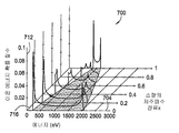
도 7A 및 도 7B는 챔버의 개별 전극들에 결합된 개별 주파수 소스들을 갖는 다른 처리 챔버와 이중 주파수 소스를 갖는 처리 챔버의 일 실시예의 이온 에너지 분포를 비교하는 그래프들이다.7A and 7B are graphs comparing the ion energy distribution of one embodiment of a processing chamber with a dual frequency source and another processing chamber with separate frequency sources coupled to the individual electrodes of the chamber.
이해를 돕기 위해, 도면들에 공통인 동일 엘리먼트들을 지칭하도록, 가능한 동일한 참조 부호들이 사용되었다.For ease of understanding, the same reference numerals have been used where possible to refer to the same elements that are common to the figures.
본 발명은 이중 주파수 RF 소스를 이용한 플라즈마 강화 반도체 처리 챔버의 플라즈마 특성들을 형성 및 제어하기 위한 방법 및 장치이다. 플라즈마 강화 반도체 처리 챔버들은 일반적으로 2개의 주파수들에서 공급되는 전력을 사용한다: 플라즈마 여기(excitation) 및 이온 해리를 위한 고주파수; 및 플라즈마 외피 변조를 위한 저주파수. 일 실시예에서, 본 발명은 플라즈마를 생성하기 위해 단일 RF 소스로부터 생성된 2개의 고주파수 입력들을 이용한다. 예를 들어, 외피 조절과 같은 플라즈마의 하나 이상의 특성들은 2개의 입력 신호들 간의 주파수 차이와 동일한 플라즈마 외피의 저주파수 성분을 생성하는 웨이브 패킷(wave packet) 현상의 이용에 의해 제어된다. The present invention is a method and apparatus for forming and controlling plasma characteristics of a plasma enhanced semiconductor processing chamber using a dual frequency RF source. Plasma enhanced semiconductor processing chambers generally use power supplied at two frequencies: high frequency for plasma excitation and ion dissociation; And low frequency for plasma envelope modulation. In one embodiment, the present invention uses two high frequency inputs generated from a single RF source to generate a plasma. For example, one or more characteristics of the plasma, such as skin conditioning, are controlled by the use of a wave packet phenomenon that produces a low frequency component of the plasma skin that is equal to the frequency difference between the two input signals.
도 1은 이중 주파수 RF 소스를 갖는 플라즈마 강화 반도체 처리 챔버의 간략화된 블록도를 도시한다. 본 발명에 따른 플라즈마 강화 반도체 처리 챔버(100)는 챔버(102), 이중 주파수 RF 전원(104), 및 단일 정합 회로(106)를 포함한다. 챔버(102)는 정합 회로(106) 및 접지된 전극(110)을 통해 RF 전원(104)에 결합된 전력공급되는 전극(108)을 포함한다. 챔버(102)는 감소된 RF 기반설비인 것을 제외하고는 종래의 플라즈마 강화 처리 챔버와 유사하다.1 shows a simplified block diagram of a plasma enhanced semiconductor processing chamber having a dual frequency RF source. The plasma enhanced
RF 전원(104)은 이중 주파수 여기를 통한 RF 생성기이다. RF 전원(104)은 일반적으로 약 100KHz 내지 약 200MHz 범위의 2개의 주파수들을 생성할 수 있다. RF 전원(104)은 또한 일반적으로 5000W까지의 연속적인 또는 펄스화된 전력을 생성할 수 있다. 특정한 일 실시예에서, RF 전원은 약 13MHz 및 약 14MHz를 생성하고, 약 3KW에서 각각의 주파수를 생성한다.
동작시, RF 전원(104)에 의해 생성되는 2개의 주파수들은 일반적으로 RF 전원(104)의 출력에서 대략 동일한 크기를 갖고, 각각의 개별 주파수들이 고주파수 플라즈마 여기, 이온 해리, 이온 에너지 분포 함수 등과 같은 규정된 서브세트의 플라즈마 특성들을 제어하도록, 선택된다. 또한, 주파수들은 이하에서 추가로 논의되는 것처럼, 정합 회로(106)를 통한 공통 정합을 허용하도록 서로 인접하도록 선택된다. 선택된 2개의 주파수들 간의 차이는 저주파수 플라즈마 여기, 외피 전압 변조 등과 같은 제 2 서브세트의 플라즈마 특성들을 제어하는데 사용될 수 있는 웨이브 패킷 효과를 형성한다. 이러한 웨이브 패킷 효과는 도 2 및 도 3에 도시된다. 선택적으로, RF 전원(104)에 의해 생성되는 2개의 주파수 신호들의 크기 사이의 비율은 2개의 주파수들 간에 차이에 의해 생성되는 웨이브 패킷 효과의 크기를 제어하기 위해 가변될 수 있다. In operation, the two frequencies generated by the
이중 주파수들 및 이들의 차이로 생성되는 웨이브 패킷 효과에 의해 제어되는 플라즈마 특성들은 중첩될 수 있다(즉, 플라즈마 여기, 이온 에너지 분포 함수, 외피 변조 등과 같이, 제어되는 특성들의 일부 또는 전부는 RF 전원(104)에 의해 제공되는 이중 주파수들, 및 2개의 주파수들간의 차이에 의해 생성되는 결과적인 웨이브 패킷 효과에 의해, 적어도 부분적으로 제어될 수 있다). 더욱이, 동일하거나 다른 플라즈마 특성들 또는 플라즈마 특성들의 서브세트들은 플라즈마에 결합된 부가적인 RF 신호들에 의해 제어될 수 있다. 예를 들어, 플라즈마 특성들의 제 3 서브세트는 이하에서 도 6을 참조로 논의되는 것처럼, 챔버에 배치된 다른 전극에 결합된 다른 RF 전원에 의해 제공되는 RF 신호에 의해 제어될 수 있다.Plasma properties controlled by the wave packet effect generated by the dual frequencies and their differences may overlap (ie, plasma power, ion energy distribution function, envelope modulation, etc.), some or all of the controlled properties may be RF power supplies. Can be at least partially controlled by the dual frequencies provided by 104 and the resulting wave packet effect generated by the difference between the two frequencies). Moreover, the same or different plasma characteristics or subsets of plasma characteristics may be controlled by additional RF signals coupled to the plasma. For example, the third subset of plasma characteristics may be controlled by an RF signal provided by another RF power source coupled to another electrode disposed in the chamber, as discussed below with reference to FIG. 6.
도 2는 주파수(220)의 함수로서 플라즈마 챔버(102)의 전력공급되는 전극(108)상에 입사하는 입력 파형에 대한 푸리에(Fourier) 성분의 크기(210)를 도시하고, 도 3은 주파수(320)의 함수로서 외피의 결과적인 주파수 성분들의 진폭(310)을 나타내는, 외피 전압 파형(300)의 주파수 분석을 도시한다. 도 2에서 알 수 있는 것처럼, 입력 파형(200)의 주파수 스펙트럼은 RF 전원(104)에 의해 생성되는 주파수 1 및 주파수 2에 해당하는, 2개의 기대 피크들(expected peaks)(202, 204)을 포함한다. 그러나, 도 3에서 알 수 있는 것처럼, 저주파수 한계선(term)(피크 306)은 RF 전원(104)으로부터의 제 1 구동 주파수들(피크 302 및 304) 및 이들의 기대 고조파들(expected harmonics)과 함께 외피에 생성된다. 외피는 RF 믹서(mixer) 다이오드가 입력 RF 신호들에 영향을 주는 것과 동일한 방식으로 RF 신호들에 영향을 주는 비선형 특성 곡선을 갖고, 즉 내부 변조 주파수 성분은 2개의 입력 주파수들 간의 차이와 동일하게 형성된다. 따라서, 저주파수 한계선(피크 306)은 RF 전원(104)에 의해 생성되는 2개의 주파수들 간의 차이와 동일하다.FIG. 2 shows the
RF 전원(104)에 의해 생성되는 구동 주파수들의 최대 차이는 정합 회로(106)의 특성들에 의해 결정된다. 특히, 정합 회로(106)의 공진 대역폭은 구동 주파수들 사이의 중심에 있다. 정합 회로(106)는 두 주파수들을 전극(108) 및 플라즈마에 효율적으로 결합시키는 대역폭을 규정하는 Q를 가져야 한다. 2개의 구동 주파 수들이 정합 회로의 대역폭내에 실질적으로 포함된다면, RF 기반설비는 2개의 개별 주파수들을 지원할 수 있다. 그러한 프로세스 향상을 위해 전형적으로 사용되는 저주파수 범위의 크기의 주파수 차이들은 전류 정합 기술과 함께 이용가능하다.The maximum difference in driving frequencies generated by the
도 4A는 전형적인 L-타입 정합을 위한 크기 면에서 반사 계수의 그래프(400)를 나타내고, 축 404에 따른 데시벨(dB)들의 반사 계수 크기에 대한 축 402에 따른 MHz의 주파수를 도시한다. 주파수들은 반사 계수 크기가 작고 점들(406, 408)로 도시된 것처럼, RF 전원(104)에 의해 생성되는 주파수 1 및 주파수 2에 대해 실질적으로 동일하도록, 선택되어야 한다. 4A shows a
도 4B는 전형적인 L-타입 정합을 위한 실제/가상 공간에서 주파수들의 위치를 도시한다. 도 4B에 도시된 예시적인 Smith 차트(450)는 표준 RF 전원들에 일반적으로 존재하는 바와 같은 50Ω 부하를 도시한다. 주파수들은 도 4B의 예시적인 주파수들(454, 456)에 의해 도시된 것처럼, 상당히 낮은 반사 전력을 제공하기 위해, 가능한 Smith 차트(450)의 중심(452)에 근접하게 감소하도록 선택되어야 한다.4B shows the location of frequencies in real / virtual space for a typical L-type match. The example Smith chart 450 shown in FIG. 4B shows a 50 kV load as is generally present in standard RF power supplies. The frequencies should be chosen to decrease as close to the
예를 들어, 60MHz 및 2MHz에서 플라즈마를 여기시키기 위해, 이들 주파수들을 위한 2개의 개별 전원들 및 정합들이 표준 플라즈마 강화 반도체 처리 챔버에 일반적으로 요구된다. 그러나, 본 발명에서는, 선택된 2개의 주파수들이 고주파수 값 주위에 중심을 두고, 즉 2개의 주파수들의 평균은 고주파수 성분이며, 2개의 주파수들은 목표된 보다 낮은 주파수와 동일한 길이(span)만큼 차이가 있다. 59MHz 및 61MHz에서의 주파수들은 공통의 정합 회로(106)를 통해 공통 RF 소스(104)로부터 공급되고, 이에 따라 플라즈마 여기(59MHz 및 61MHz 신호들) 및 2MHz 변조 신호 를 플라즈마 외피에 대해 인가한다. 이러한 구성은 2개의 소스들, 및 2개의 독립적인 정합 엘리먼트들 또는 단일 소스에 대한 단일 이중 주파수 정합 엘리먼트, 및 하나의 단일 주파수 정합 엘리먼트를 갖는 현재의 이중 주파수 기술의 RF 기반설비를 감소시키고, 프로세스 장점을 훼손함이 없이 시스템의 비용을 현저히 감소시킨다.For example, to excite the plasma at 60 MHz and 2 MHz, two separate power supplies and matching for these frequencies are generally required in a standard plasma enhanced semiconductor processing chamber. However, in the present invention, the two selected frequencies are centered around the high frequency value, ie the average of the two frequencies is a high frequency component, and the two frequencies differ by the same span as the desired lower frequency. The frequencies at 59 MHz and 61 MHz are supplied from a
다른 예에서, RF 전원(104)으로부터 전력공급된 전극(108)으로 공급되는 2개의 주파수들은 내부 변조 주파수 성분에 의해 제어되는 것과 동일한 플라즈마 특성을 제어하도록 선택될 수 있다(즉, 2개의 제 1 주파수들간의 차이는 RF 전원(104)에 의해 생성되는 제 1 주파수들과 동일한 플라즈마 파라미터를 조정한다).In another example, the two frequencies supplied from the
일 실시예에서, 이온 에너지 분포 함수는 제 1 주파수들 및 내부 변조 주파수 성분에 의해 제어될 수 있다. 즉, 이온 에너지 분포 함수는 제 1 주파수들의 선택 및 제 1 주파수들간의 차이의 제어에 의해 제어될 수 있다. 구체적으로는, RF 전원(104)으로부터 전극(108)으로 공급되는 2개의 주파수들은 외피가 2개의 주파수들에서 각각 진동하도록 한다. 또한, 외피 진동은 2개의 주파수들간의 차이에서 특성 주파수를 갖는다(즉, 내부 변조 주파수 성분으로 인해).In one embodiment, the ion energy distribution function may be controlled by the first frequencies and the internal modulation frequency component. That is, the ion energy distribution function can be controlled by selection of the first frequencies and control of the difference between the first frequencies. Specifically, the two frequencies supplied from the
플라즈마 외피가 이온이 응답할 수 있는 것보다 더 빨리 진동하면, 이온은 시간 평균, 또는 외피의 DC 성분에 대해 반응하고, RF 진동으로 인한 외피의 전위 변화 때문에 이온이 경험하는 궤도에서 편향(deflection)의 양은 역 외피 주파수와 동일하다(예, 외피 진동 주파수가 높아지면, 외피를 통과하는 이온 속도의 변조가 적어진다). 주파수 차이의 역수가 플라즈마 벌크로부터 가속될 때 이온이 외피를 통과하는데 걸리는 시간보다 더 작도록 주파수들을 선택함으로써, 주파수 차이의 외피 진동은 이온의 최종 에너지에 시간 가변성을 부가할 수 있다. 따라서, 이온 에너지 분포 함수는 외피에서 이온 전이 시간에 걸치는 외피의 진동 주파수들을 제어함으로써 제어될 수 있다(예, 외피의 진동 주파수들은 외피에서 이온 전이 시간의 역수 초과 및 미만이다).If the plasma envelope vibrates faster than the ions can respond, the ions respond to a time average, or to the DC component of the envelope, and deflection in the orbit experienced by the ions due to the potential change of the envelope due to RF vibration. The amount of is equal to the inverse skin frequency (e.g., the higher the skin vibration frequency, the less the modulation of ion velocity through the skin). By selecting the frequencies so that the reciprocal of the frequency difference is less than the time it takes for the ions to pass through the envelope when the acceleration from the plasma bulk, the envelope vibration of the frequency difference can add time variability to the final energy of the ion. Thus, the ion energy distribution function can be controlled by controlling the vibration frequencies of the skin over the ion transition time in the skin (eg, the vibration frequencies of the skin are above and below the inverse of the ion transition time in the skin).
일 실시예에서, 제 1 주파수들은 이온 전이 시간의 역수 보다 더 크게 선택될 수 있다. 또한, 제 1 주파수들간의 차이는 이온 전이 시간의 역수 미만으로 선택될 수 있다. 제 1 주파수들 및 제 1 주파수들간의 차이를 제어하면, 이온 에너지 분포 함수를 제어할 수 있다.In one embodiment, the first frequencies may be selected to be greater than the inverse of the ion transition time. In addition, the difference between the first frequencies may be selected to be less than the inverse of the ion transition time. By controlling the difference between the first frequencies and the first frequencies, the ion energy distribution function can be controlled.
예를 들어, 일 실시예에서, RF 전원(104)은 약 13.56MHz 및 약 13.86MHz의 제 1 주파수들을 갖는 2개의 신호들을 전극(108)에 생성할 수 있다. 이는 플라즈마 외피가 각각 13.56MHz 및 13.86MHz에서 진동하도록 한다. 또한, 외피는 2개의 제 1 주파수들간의 차이에서 발생되는 내부 변조 주파수 성분으로 인해 300KHz에서 특성 진동을 갖는다.For example, in one embodiment,
도 7A 및 도 7B에 도시된 그래프들의 비교를 통해 알 수 있는 것처럼, 전술한 바와 같이, 약 13.56MHz 및 약 13.86MHz의 제 1 주파수들을 제공하는 이중 주파수 소스를 갖는 처리 챔버에 대한 이온 에너지 분포 함수(700)(도 7A에 도시됨)는 2개의 개별 RF 전원들을 갖는 처리 챔버로부터 발생되는 이온 에너지 분포 함수(710)(도 7B에 도시됨)와 매우 유사하다. 따라서, 본 발명의 이중 주파수 소스 구성은 바람직하게도, 처리 챔버의 상부 및 하부 전극에 결합된 개별 RF 전원들을 갖는 챔버들과 비교하여 이온 에너지 분포 함수의 유사한 제어를 허용할 수 있고, 이에 따라 처리 챔버와 연관된 복잡성 및 하드웨어 비용을 현저히 감소시킬 수 있다.As can be seen from the comparison of the graphs shown in FIGS. 7A and 7B, as described above, the ion energy distribution function for a processing chamber having a dual frequency source providing first frequencies of about 13.56 MHz and about 13.86 MHz 700 (shown in FIG. 7A) is very similar to the ion energy distribution function 710 (shown in FIG. 7B) generated from the processing chamber with two separate RF power sources. Thus, the dual frequency source configuration of the present invention preferably allows similar control of the ion energy distribution function as compared to chambers with separate RF power supplies coupled to the upper and lower electrodes of the processing chamber, thus The complexity and hardware costs associated with this can be significantly reduced.
또한, 제 1 주파수들 및 내부 변조 주파수 성분의 상대적 크기가 이온 에너지 분포 함수를 제어하는데 추가적으로 사용될 수 있다. 예를 들어, 2개의 제 1 주파수들의 상대적 전류 또는 상대적 전력은 내부 변조 주파수 성분의 크기를 제어하도록 선택적으로 제공될 수 있다. 구체적으로는, 2개의 제 1 주파수들이 동일한 전류로 인가될 때, 내부 변조 주파수 성분의 크기가 최대가 된다. 2개의 제 1 주파수들 중 하나의 전류를 다른 것에 대해 감소시키면, 인가되는 제로 전류에서(즉, 제 2 주파수가 없음), 내부 변조 주파수 성분이 사라질 때까지, 내부 변조 주파수 성분의 크기가 감소된다.In addition, the relative magnitude of the first frequencies and the internal modulation frequency component can additionally be used to control the ion energy distribution function. For example, the relative current or relative power of the two first frequencies may optionally be provided to control the magnitude of the internal modulation frequency component. Specifically, when the two first frequencies are applied with the same current, the magnitude of the internal modulation frequency component is maximized. Reducing the current of one of the two first frequencies relative to the other, reduces the magnitude of the internal modulation frequency component until the internal modulation frequency component disappears at the applied zero current (ie no second frequency). .
제 1 주파수들의 전류 또는 전력의 크기와 비교하여, 내부 변조 주파수 성분의 상대적 크기는 이온 에너지 분포에 추가적인 가변성을 부가하기 때문에, 상대적 크기들의 범위에 대한 이온 에너지 분포 함수의 제어를 허용한다.Compared with the magnitude of the current or power of the first frequencies, the relative magnitude of the internal modulation frequency component adds additional variability to the ion energy distribution, thus allowing control of the ion energy distribution function over a range of relative magnitudes.
본 발명의 장점에 적용될 수 있는 플라즈마 강화 반도체 처리 챔버들의 예들은 이에 제한됨이 없이, 캘리포니아 산타클레라의 어플라이드 머티어리얼스 사로부터 모두 이용가능한, Decoupled Plasma Source(DPS®, DPS® Ⅱ), EMAX™, MXP®, 및 ENABLER™ 처리 챔버들을 포함한다. EMAX™ 처리 챔버는 Shan 외에게 2000년 9월 5일자로 특허된 미국특허번호 제6,113,731호에 기술된다. MXP® 처리 챔버는 Qian 외에게 1999년 7월 9일자로 특허된 미국특허번호 제5,534,108호, 및 Pu 외에 게 1997년 10월 7일자로 특허된 미국특허번호 제5,674,321호에 기술된다. ENABLER™ 처리 챔버는 Hoffman 외에게 2003년 3월 4일자로 특허된 미국특허번호 제6,528,751호에 기술된다. 전술한 각각의 특허들은 그 전체가 본 발명에 참조로 포함된다.Examples of plasma enhanced semiconductor processing chambers that may be applied to the advantages of the present invention include, but are not limited to, Decoupled Plasma Source (DPS®, DPS® II), EMAX, all available from Applied Materials, Inc. of Santa Clara, California. ™, MXP®, and ENABLER ™ processing chambers. The EMAX ™ process chamber is described in US Pat. No. 6,113,731, issued September 5, 2000 to Shan et al. MXP® processing chambers are described in US Pat. No. 5,534,108, issued July 9, 1999 to Qian et al., And US Pat. No. 5,674,321, issued October 7, 1997 to Pu et al. The ENABLER ™ process chamber is described in US Pat. No. 6,528,751, issued March 4, 2003 to Hoffman et al. Each of the foregoing patents is incorporated herein by reference in their entirety.
도 5는 본 발명에 사용하기 적합한 에칭 반응기(500)의 예시적인 일 실시예의 개념도를 도시한다. 일 실시예에서, 에칭 반응기(500)는 전도성 몸체(벽)(534) 내에 기판 지지 페디스털(pedestal)(512)을 갖는 처리 챔버(502), 및 제어기(536)를 포함한다. 지지 페디스털(512)은 정합 회로(106)를 통해 이중 주파수 RF 전원(104)에 결합된다. (RF 전원(104) 및 정합 회로(106)는 도 1에 대하여 기술된다.)5 shows a conceptual diagram of one exemplary embodiment of an
제어기(536)는 중앙 처리 유닛(CPU)(540), 메모리(542), 및 CPU(540)를 위한 지원 회로들(544)을 포함하고, 처리 챔버(502)의 컴포넌트들의 제어 및 이에 따라 이하에서 추가적으로 상세히 논의되는 바와 같은, 에칭 프로세스의 제어를 용이하게 한다. 제어기(536)는 다양한 챔버들과 서브-프로세서들을 제어하기 위해 설정되는 산업상 이용될 수 있는 임의의 형태의 범용 컴퓨터 프로세서 중 하나일 수 있다. CPU(540)의 메모리, 또는 컴퓨터-판독가능한 매체(542)는 랜덤 액세스 메모리(RAM), 리드 온리 메모리(ROM), 플로피 디스크, 하드 디스크, 또는 로컬이나 원격의 임의의 다른 형태의 디지털 스토리지와 같은 하나 이상의 용이하게 이용가능한 메모리일 수 있다. 지원 회로들(544)은 종래의 방식으로 프로세서를 지원하기 위해 CPU(540)에 결합된다. 이러한 회로들은 캐쉬, 전원들, 클록 회로들, 입력/출 력 회로 및 서브시스템들 등을 포함한다. 진보적인 본 발명의 방법은 일반적으로 소프트웨어 루틴으로서 메모리(542)에 저장된다. 소프트웨어 루틴은 또한 CPU(540)에 의해 제어되는 하드웨어로부터 떨어져 위치된 제 2 CPU(미도시)에 의해 저장 및/또는 실행될 수도 있다.The
기본적인 에칭 동작에서, 기판(514)은 페디스털(512)상에 배치되고, 처리 가스들은 입구 포트들(516)을 통해 가스 패널(518)로부터 공급되며, 가스 혼합물(546)을 형성한다. 가스 혼합물(546)은 이중 RF 전원(104)으로부터 기판 지지 페디스털(512)로 전력을 인가함으로써 챔버(502)의 플라즈마(548)로 점화된다. RF 전원(104)에 의해 생성되는 2개의 주파수들은 플라즈마 여기 및 이온 해리를 촉진시키기 위해 고주파수 범위에서 일반적으로 선택된다. RF 전원(104)에 의해 생성되는 2개의 주파수들은 예를 들어, 플라즈마 외피를 변조시키기 위해 바람직한, 특정한 저주파수와 동일한 미리 결정된 길이(span)만큼 추가로 차이가 있다.In a basic etch operation,
전형적으로, 챔버 벽(534)은 전기적 접지(552)에 결합된다. 챔버(502)의 내부의 압력은 스로틀 밸브(550) 및 진공 펌프(520)를 이용하여 제어된다. 챔버 벽(534)의 온도는 챔버 벽(534)을 관통하는 액체-함유 도관들(미도시)을 이용하여 제어된다.Typically,
에칭 챔버들의 다른 형태들은 원격 플라즈마 소스들을 갖는 챔버들, 마이크로파 플라즈마 챔버들, 전자 사이클로트론 공명(ECR) 플라즈마 챔버들 등을 포함하여, 본 발명을 실시하는데 사용될 수 있다. 이러한 기술은 에칭으로 제한되는 것이 아니라, 증착, 어닐링, 질화, 주입 등을 포함하는 임의의 다른 플라즈마 보조 프로세스일 수 있다.Other forms of etch chambers can be used to practice the invention, including chambers with remote plasma sources, microwave plasma chambers, electron cyclotron resonance (ECR) plasma chambers, and the like. This technique is not limited to etching, but may be any other plasma assisted process including deposition, annealing, nitriding, implantation, and the like.
예를 들어, 도 6은 본 발명에 사용하기 적합한 에칭 반응기(600)의 예시적인 다른 실시예의 개념도를 도시한다. 일 실시예에서, 에칭 반응기(600)는 전도성 몸체(벽)(634)내에 기판 지지 페디스털(612)을 갖는 처리 챔버(602), 및 제어기(636)를 포함한다. 제어기(636)는 도 5를 참조로 전술한 제어기(536)와 유사하다. 지지 페디스털(612)은 정합 회로(106)를 통해 이중 주파수 RF 전원(104)에 결합된다. (RF 전원(104) 및 정합 회로(106)는 도 1에 대하여 기술된다.) 챔버(602)는 그 상부에 배치된 적어도 하나의 유도성 코일(638)을 갖는 유전체 실링(ceiling)(610)을 추가로 포함한다(2개의 코일들(638)은 도 6의 실시예에 도시된다). 유도성 코일들(638)은 제 2 정합 엘리먼트(660)를 통해 제 2 전원(662)에 결합된다. 제 2 전원(662)은 일반적으로 약 50KHz 약 13.56MHz 범위의 조정가능한 주파수에서 3000W까지의 전력을 생성할 수 있는 단일 RF 생성기이다. RF 전원(662)에 대한 주파수 범위는 유도성 결합된 상부 소스를 갖는 처리 챔버들에 일반적으로 사용되는 범위이다. 다른 범위들이 적절할 수 있고, 다른 타입들의 처리 챔버들에 본 발명과 함께 사용될 수 있다. 예를 들어, 용량성 결합된 상부 소스를 갖는 챔버에서, RF 전원은 일반적으로 200MHz만큼 높은 주파수들을 갖는 신호들을 생성한다. 선택적으로, 마이크로파 소스들은 5GHz만큼 높은 주파수들을 생성할 수 있다.For example, FIG. 6 shows a conceptual diagram of another exemplary embodiment of an
기본 에칭 동작에서, 기판(614)은 페디스털(612)상에 배치되고, 처리 가스들은 입구 포트들(616)을 통해 가스 패널(618)로부터 공급되며, 가스 혼합물(646)을 형성한다. 가스 혼합물(646)은 RF 전원(662)으로부터의 전력을 유도성 코일 들(638)로 인가하고 이중 RF 전원(104)으로부터의 전력을 기판 지지 페디스털(612)로 인가함으로써, 챔버(602)의 플라즈마(648)로 점화된다. RF 전원(104)에 의해 생성되는 2개의 주파수들은 플라즈마 여기 및 이온 해리를 촉진시키기 위해, 높은 주파수 범위에서 일반적으로 선택된다. 그러나, 전력은 이를 달성하기에 충분히 높지 않을 수 있고, RF 전원(104)은 기판(614)을 바이어스시키기 위해 주로 사용될 수 있다. RF 전원(104)에 의해 생성되는 2개의 주파수들은 예를 들어, 플라즈마 외피를 변조시키기 위해 바람직한, 특정한 저주파수와 동일한 미리 결정된 길이(span)만큼 추가로 차이가 있다. RF 전원(662)과 조합되는 이중 주파수 RF 전원(104)의 사용은 챔버(602)의 반도체 기판(614)의 처리를 제어하기 위한 보다 많은 프로세스 제어 변수들을 제공한다.In a basic etch operation,
전형적으로, 챔버 벽(634)은 전기적 접지(652)에 결합된다. 챔버(602)의 내부의 압력은 스로틀 밸브(650) 및 진공 펌프(620)를 이용하여 제어된다. 챔버 벽(634)의 온도는 챔버 벽(634)을 관통하는 액체-함유 도관들(미도시)을 이용하여 제어된다.Typically,
전술한 상세한 설명은 본 발명의 예시적인 실시예에 관한 것이지만, 본 발명의 다른 실시예들 및 추가적인 실시예들이 그 기본 범주를 벗어남이 없이 안출될 수 있다.While the foregoing detailed description is directed to exemplary embodiments of the invention, other and further embodiments of the invention may be devised without departing from its basic scope.
Claims (20)
Applications Claiming Priority (4)
| Application Number | Priority Date | Filing Date | Title |
|---|---|---|---|
| US67904205P | 2005-05-09 | 2005-05-09 | |
| US60/679,042 | 2005-05-09 | ||
| US11/416,468 US7510665B2 (en) | 2003-08-15 | 2006-05-02 | Plasma generation and control using dual frequency RF signals |
| US11/416,468 | 2006-05-02 |
Publications (1)
| Publication Number | Publication Date |
|---|---|
| KR20070102623A true KR20070102623A (en) | 2007-10-18 |
Family
ID=37396865
Family Applications (1)
| Application Number | Title | Priority Date | Filing Date |
|---|---|---|---|
| KR1020077021009A KR20070102623A (en) | 2005-05-09 | 2006-05-04 | Plasma generation and control using dual frequency rf signals |
Country Status (5)
| Country | Link |
|---|---|
| US (1) | US7510665B2 (en) |
| JP (1) | JP2008544480A (en) |
| KR (1) | KR20070102623A (en) |
| TW (1) | TWI344321B (en) |
| WO (1) | WO2006121744A1 (en) |
Families Citing this family (17)
| Publication number | Priority date | Publication date | Assignee | Title |
|---|---|---|---|---|
| CN100362619C (en) | 2005-08-05 | 2008-01-16 | 中微半导体设备(上海)有限公司 | RF matching coupling network for vacuum reaction chamber and its configuration method |
| US7758763B2 (en) * | 2006-10-31 | 2010-07-20 | Applied Materials, Inc. | Plasma for resist removal and facet control of underlying features |
| US8994270B2 (en) | 2008-05-30 | 2015-03-31 | Colorado State University Research Foundation | System and methods for plasma application |
| WO2011123124A1 (en) | 2010-03-31 | 2011-10-06 | Colorado State University Research Foundation | Liquid-gas interface plasma device |
| JP2011521735A (en) | 2008-05-30 | 2011-07-28 | コロラド ステート ユニバーシティ リサーチ ファンデーション | System, method and apparatus for generating plasma |
| JP2011522381A (en) | 2008-05-30 | 2011-07-28 | コロラド ステート ユニバーシティ リサーチ ファンデーション | Plasma-based chemical source apparatus and method of use thereof |
| JP5398058B2 (en) * | 2008-10-31 | 2014-01-29 | 株式会社ダイヘン | High frequency power supply |
| US20100326602A1 (en) * | 2009-06-30 | 2010-12-30 | Intevac, Inc. | Electrostatic chuck |
| US8222822B2 (en) * | 2009-10-27 | 2012-07-17 | Tyco Healthcare Group Lp | Inductively-coupled plasma device |
| CA2794902A1 (en) | 2010-03-31 | 2011-10-06 | Colorado State University Research Foundation | Liquid-gas interface plasma device |
| JP5916056B2 (en) * | 2010-08-23 | 2016-05-11 | 東京エレクトロン株式会社 | Plasma processing method and plasma processing apparatus |
| US9532826B2 (en) | 2013-03-06 | 2017-01-03 | Covidien Lp | System and method for sinus surgery |
| US9555145B2 (en) | 2013-03-13 | 2017-01-31 | Covidien Lp | System and method for biofilm remediation |
| US9284210B2 (en) * | 2014-03-31 | 2016-03-15 | Corning Incorporated | Methods and apparatus for material processing using dual source cyclonic plasma reactor |
| US10312048B2 (en) * | 2016-12-12 | 2019-06-04 | Applied Materials, Inc. | Creating ion energy distribution functions (IEDF) |
| US10395896B2 (en) | 2017-03-03 | 2019-08-27 | Applied Materials, Inc. | Method and apparatus for ion energy distribution manipulation for plasma processing chambers that allows ion energy boosting through amplitude modulation |
| WO2022047227A2 (en) * | 2020-08-28 | 2022-03-03 | Plasma Surgical Investments Limited | Systems, methods, and devices for generating predominantly radially expanded plasma flow |
Family Cites Families (37)
| Publication number | Priority date | Publication date | Assignee | Title |
|---|---|---|---|---|
| US4579618A (en) | 1984-01-06 | 1986-04-01 | Tegal Corporation | Plasma reactor apparatus |
| US4585516A (en) | 1985-03-04 | 1986-04-29 | Tegal Corporation | Variable duty cycle, multiple frequency, plasma reactor |
| DE3733135C1 (en) | 1987-10-01 | 1988-09-22 | Leybold Ag | Device for coating or etching using a plasma |
| US5556501A (en) | 1989-10-03 | 1996-09-17 | Applied Materials, Inc. | Silicon scavenger in an inductively coupled RF plasma reactor |
| JPH04901A (en) | 1990-04-18 | 1992-01-06 | Mitsubishi Electric Corp | Method and device for feeding high frequency power for plasma apparatus |
| US5065118A (en) | 1990-07-26 | 1991-11-12 | Applied Materials, Inc. | Electronically tuned VHF/UHF matching network |
| US5280154A (en) | 1992-01-30 | 1994-01-18 | International Business Machines Corporation | Radio frequency induction plasma processing system utilizing a uniform field coil |
| KR100324792B1 (en) | 1993-03-31 | 2002-06-20 | 히가시 데쓰로 | Plasma processing apparatus |
| KR100302167B1 (en) | 1993-11-05 | 2001-11-22 | 히가시 데쓰로 | Plasma Treatment Equipment and Plasma Treatment Methods |
| JP2654340B2 (en) | 1993-11-11 | 1997-09-17 | 株式会社フロンテック | Substrate surface potential measuring method and plasma apparatus |
| US5512130A (en) | 1994-03-09 | 1996-04-30 | Texas Instruments Incorporated | Method and apparatus of etching a clean trench in a semiconductor material |
| EP0715334B1 (en) | 1994-11-30 | 1999-04-14 | Applied Materials, Inc. | Plasma reactors for processing semiconductor wafers |
| US5534751A (en) | 1995-07-10 | 1996-07-09 | Lam Research Corporation | Plasma etching apparatus utilizing plasma confinement |
| JP3119172B2 (en) | 1995-09-13 | 2000-12-18 | 日新電機株式会社 | Plasma CVD method and apparatus |
| JPH0982495A (en) * | 1995-09-18 | 1997-03-28 | Toshiba Corp | Plasma producing device and method |
| US5817534A (en) | 1995-12-04 | 1998-10-06 | Applied Materials, Inc. | RF plasma reactor with cleaning electrode for cleaning during processing of semiconductor wafers |
| JP3808973B2 (en) | 1996-05-15 | 2006-08-16 | 株式会社ダイヘン | Plasma processing equipment |
| US6500314B1 (en) | 1996-07-03 | 2002-12-31 | Tegal Corporation | Plasma etch reactor and method |
| US6048435A (en) | 1996-07-03 | 2000-04-11 | Tegal Corporation | Plasma etch reactor and method for emerging films |
| JP3220383B2 (en) | 1996-07-23 | 2001-10-22 | 東京エレクトロン株式会社 | Plasma processing apparatus and method |
| US6113731A (en) | 1997-01-02 | 2000-09-05 | Applied Materials, Inc. | Magnetically-enhanced plasma chamber with non-uniform magnetic field |
| US6126778A (en) | 1998-07-22 | 2000-10-03 | Micron Technology, Inc. | Beat frequency modulation for plasma generation |
| US5985375A (en) | 1998-09-03 | 1999-11-16 | Micron Technology, Inc. | Method for pulsed-plasma enhanced vapor deposition |
| US6642149B2 (en) | 1998-09-16 | 2003-11-04 | Tokyo Electron Limited | Plasma processing method |
| US6222718B1 (en) | 1998-11-12 | 2001-04-24 | Lam Research Corporation | Integrated power modules for plasma processing systems |
| US6196855B1 (en) * | 1999-08-13 | 2001-03-06 | Umax Data Systems Inc. | Guiding mechanism for guiding flat cable between two traveling modules |
| US6193855B1 (en) | 1999-10-19 | 2001-02-27 | Applied Materials, Inc. | Use of modulated inductive power and bias power to reduce overhang and improve bottom coverage |
| US7030335B2 (en) | 2000-03-17 | 2006-04-18 | Applied Materials, Inc. | Plasma reactor with overhead RF electrode tuned to the plasma with arcing suppression |
| US6507155B1 (en) | 2000-04-06 | 2003-01-14 | Applied Materials Inc. | Inductively coupled plasma source with controllable power deposition |
| US6506289B2 (en) | 2000-08-07 | 2003-01-14 | Symmorphix, Inc. | Planar optical devices and methods for their manufacture |
| JP2002246368A (en) | 2001-02-14 | 2002-08-30 | Anelva Corp | System for processing a wafer using radially uniform plasma over wafer surface |
| JP2003073836A (en) | 2001-08-28 | 2003-03-12 | Canon Inc | Method and apparatus for vacuum treatment |
| US6887340B2 (en) | 2001-11-13 | 2005-05-03 | Lam Research Corporation | Etch rate uniformity |
| TWI241868B (en) | 2002-02-06 | 2005-10-11 | Matsushita Electric Ind Co Ltd | Plasma processing method and apparatus |
| US7431857B2 (en) | 2003-08-15 | 2008-10-07 | Applied Materials, Inc. | Plasma generation and control using a dual frequency RF source |
| US7838430B2 (en) | 2003-10-28 | 2010-11-23 | Applied Materials, Inc. | Plasma control using dual cathode frequency mixing |
| US20050241762A1 (en) | 2004-04-30 | 2005-11-03 | Applied Materials, Inc. | Alternating asymmetrical plasma generation in a process chamber |
-
2006
- 2006-05-02 US US11/416,468 patent/US7510665B2/en active Active
- 2006-05-04 JP JP2008511180A patent/JP2008544480A/en active Pending
- 2006-05-04 KR KR1020077021009A patent/KR20070102623A/en not_active Application Discontinuation
- 2006-05-04 WO PCT/US2006/017075 patent/WO2006121744A1/en active Application Filing
- 2006-05-05 TW TW095116153A patent/TWI344321B/en not_active IP Right Cessation
Also Published As
| Publication number | Publication date |
|---|---|
| US7510665B2 (en) | 2009-03-31 |
| TWI344321B (en) | 2011-06-21 |
| TW200704289A (en) | 2007-01-16 |
| JP2008544480A (en) | 2008-12-04 |
| US20060266735A1 (en) | 2006-11-30 |
| WO2006121744A1 (en) | 2006-11-16 |
Similar Documents
| Publication | Publication Date | Title |
|---|---|---|
| KR20070102623A (en) | Plasma generation and control using dual frequency rf signals | |
| US7431857B2 (en) | Plasma generation and control using a dual frequency RF source | |
| US6726804B2 (en) | RF power delivery for plasma processing using modulated power signal | |
| KR102038617B1 (en) | Plasma treatment method and plasma treatment device | |
| US5900699A (en) | Plasma generator with a shield interposing the antenna | |
| KR100255703B1 (en) | Device of plasma using electromagnetic rf | |
| KR101929675B1 (en) | Plasma processing apparatus | |
| US20040050495A1 (en) | Plasma processing apparatus and plasma processing method | |
| KR101938151B1 (en) | Plasma processing apparatus and plasma processing method | |
| JPH04354867A (en) | Plasma treating device | |
| KR100333220B1 (en) | Magnetically reinforced medium-capacity plasma generators and related methods | |
| US11056316B2 (en) | Radio frequency pulse matching method and device thereof and pulsing plasma generation system | |
| TW201435964A (en) | Method for matching radio frequency pulse power in vacuum processing chamber and its device | |
| JP4051209B2 (en) | High frequency plasma processing apparatus and high frequency plasma processing method | |
| US5470426A (en) | Plasma processing apparatus | |
| JP4653395B2 (en) | Plasma processing equipment | |
| JP3599670B2 (en) | Plasma processing method and apparatus | |
| JP3563054B2 (en) | Plasma processing apparatus and method | |
| CN101147237A (en) | Plasma generation and control using dual frequency RF signals | |
| KR102467966B1 (en) | Hybrid plasma generator and control method of hybrid plasma generator | |
| JPH07135096A (en) | Plasma processing device | |
| JP2001267296A (en) | Plasma treatment system | |
| KR20050087138A (en) | Hybrid antenna for plasma | |
| KR20220031988A (en) | Plasma treatment apparatus and plasma treatment method | |
| JPH0774160A (en) | Microwave plasma treating equipment |
Legal Events
| Date | Code | Title | Description |
|---|---|---|---|
| A201 | Request for examination | ||
| E902 | Notification of reason for refusal | ||
| E601 | Decision to refuse application |