KR101541505B1 - Multilayer ceramic electronic component - Google Patents
Multilayer ceramic electronic component Download PDFInfo
- Publication number
- KR101541505B1 KR101541505B1 KR1020137014554A KR20137014554A KR101541505B1 KR 101541505 B1 KR101541505 B1 KR 101541505B1 KR 1020137014554 A KR1020137014554 A KR 1020137014554A KR 20137014554 A KR20137014554 A KR 20137014554A KR 101541505 B1 KR101541505 B1 KR 101541505B1
- Authority
- KR
- South Korea
- Prior art keywords
- pair
- thickness
- multilayer ceramic
- width direction
- internal electrodes
- Prior art date
Links
Images


Classifications
-
- H—ELECTRICITY
- H01—ELECTRIC ELEMENTS
- H01G—CAPACITORS; CAPACITORS, RECTIFIERS, DETECTORS, SWITCHING DEVICES OR LIGHT-SENSITIVE DEVICES, OF THE ELECTROLYTIC TYPE
- H01G4/00—Fixed capacitors; Processes of their manufacture
- H01G4/002—Details
- H01G4/018—Dielectrics
- H01G4/06—Solid dielectrics
- H01G4/08—Inorganic dielectrics
- H01G4/12—Ceramic dielectrics
- H01G4/1209—Ceramic dielectrics characterised by the ceramic dielectric material
-
- H—ELECTRICITY
- H01—ELECTRIC ELEMENTS
- H01G—CAPACITORS; CAPACITORS, RECTIFIERS, DETECTORS, SWITCHING DEVICES OR LIGHT-SENSITIVE DEVICES, OF THE ELECTROLYTIC TYPE
- H01G4/00—Fixed capacitors; Processes of their manufacture
- H01G4/002—Details
- H01G4/258—Temperature compensation means
-
- H—ELECTRICITY
- H01—ELECTRIC ELEMENTS
- H01G—CAPACITORS; CAPACITORS, RECTIFIERS, DETECTORS, SWITCHING DEVICES OR LIGHT-SENSITIVE DEVICES, OF THE ELECTROLYTIC TYPE
- H01G4/00—Fixed capacitors; Processes of their manufacture
- H01G4/002—Details
- H01G4/005—Electrodes
-
- H—ELECTRICITY
- H01—ELECTRIC ELEMENTS
- H01G—CAPACITORS; CAPACITORS, RECTIFIERS, DETECTORS, SWITCHING DEVICES OR LIGHT-SENSITIVE DEVICES, OF THE ELECTROLYTIC TYPE
- H01G4/00—Fixed capacitors; Processes of their manufacture
- H01G4/002—Details
- H01G4/005—Electrodes
- H01G4/012—Form of non-self-supporting electrodes
-
- H—ELECTRICITY
- H01—ELECTRIC ELEMENTS
- H01G—CAPACITORS; CAPACITORS, RECTIFIERS, DETECTORS, SWITCHING DEVICES OR LIGHT-SENSITIVE DEVICES, OF THE ELECTROLYTIC TYPE
- H01G4/00—Fixed capacitors; Processes of their manufacture
- H01G4/002—Details
- H01G4/018—Dielectrics
- H01G4/06—Solid dielectrics
- H01G4/08—Inorganic dielectrics
- H01G4/12—Ceramic dielectrics
-
- H—ELECTRICITY
- H01—ELECTRIC ELEMENTS
- H01G—CAPACITORS; CAPACITORS, RECTIFIERS, DETECTORS, SWITCHING DEVICES OR LIGHT-SENSITIVE DEVICES, OF THE ELECTROLYTIC TYPE
- H01G4/00—Fixed capacitors; Processes of their manufacture
- H01G4/30—Stacked capacitors
-
- H—ELECTRICITY
- H05—ELECTRIC TECHNIQUES NOT OTHERWISE PROVIDED FOR
- H05K—PRINTED CIRCUITS; CASINGS OR CONSTRUCTIONAL DETAILS OF ELECTRIC APPARATUS; MANUFACTURE OF ASSEMBLAGES OF ELECTRICAL COMPONENTS
- H05K3/00—Apparatus or processes for manufacturing printed circuits
- H05K3/10—Apparatus or processes for manufacturing printed circuits in which conductive material is applied to the insulating support in such a manner as to form the desired conductive pattern
- H05K3/12—Apparatus or processes for manufacturing printed circuits in which conductive material is applied to the insulating support in such a manner as to form the desired conductive pattern using thick film techniques, e.g. printing techniques to apply the conductive material or similar techniques for applying conductive paste or ink patterns
- H05K3/1283—After-treatment of the printed patterns, e.g. sintering or curing methods
- H05K3/1291—Firing or sintering at relative high temperatures for patterns on inorganic boards, e.g. co-firing of circuits on green ceramic sheets
-
- H—ELECTRICITY
- H05—ELECTRIC TECHNIQUES NOT OTHERWISE PROVIDED FOR
- H05K—PRINTED CIRCUITS; CASINGS OR CONSTRUCTIONAL DETAILS OF ELECTRIC APPARATUS; MANUFACTURE OF ASSEMBLAGES OF ELECTRICAL COMPONENTS
- H05K3/00—Apparatus or processes for manufacturing printed circuits
- H05K3/46—Manufacturing multilayer circuits
- H05K3/4611—Manufacturing multilayer circuits by laminating two or more circuit boards
- H05K3/4626—Manufacturing multilayer circuits by laminating two or more circuit boards characterised by the insulating layers or materials
- H05K3/4629—Manufacturing multilayer circuits by laminating two or more circuit boards characterised by the insulating layers or materials laminating inorganic sheets comprising printed circuits, e.g. green ceramic sheets
-
- H—ELECTRICITY
- H05—ELECTRIC TECHNIQUES NOT OTHERWISE PROVIDED FOR
- H05K—PRINTED CIRCUITS; CASINGS OR CONSTRUCTIONAL DETAILS OF ELECTRIC APPARATUS; MANUFACTURE OF ASSEMBLAGES OF ELECTRICAL COMPONENTS
- H05K3/00—Apparatus or processes for manufacturing printed circuits
- H05K3/46—Manufacturing multilayer circuits
- H05K3/4644—Manufacturing multilayer circuits by building the multilayer layer by layer, i.e. build-up multilayer circuits
- H05K3/4664—Adding a circuit layer by thick film methods, e.g. printing techniques or by other techniques for making conductive patterns by using pastes, inks or powders
-
- H—ELECTRICITY
- H05—ELECTRIC TECHNIQUES NOT OTHERWISE PROVIDED FOR
- H05K—PRINTED CIRCUITS; CASINGS OR CONSTRUCTIONAL DETAILS OF ELECTRIC APPARATUS; MANUFACTURE OF ASSEMBLAGES OF ELECTRICAL COMPONENTS
- H05K1/00—Printed circuits
- H05K1/16—Printed circuits incorporating printed electric components, e.g. printed resistor, capacitor, inductor
- H05K1/162—Printed circuits incorporating printed electric components, e.g. printed resistor, capacitor, inductor incorporating printed capacitors
-
- H—ELECTRICITY
- H05—ELECTRIC TECHNIQUES NOT OTHERWISE PROVIDED FOR
- H05K—PRINTED CIRCUITS; CASINGS OR CONSTRUCTIONAL DETAILS OF ELECTRIC APPARATUS; MANUFACTURE OF ASSEMBLAGES OF ELECTRICAL COMPONENTS
- H05K3/00—Apparatus or processes for manufacturing printed circuits
- H05K3/10—Apparatus or processes for manufacturing printed circuits in which conductive material is applied to the insulating support in such a manner as to form the desired conductive pattern
- H05K3/12—Apparatus or processes for manufacturing printed circuits in which conductive material is applied to the insulating support in such a manner as to form the desired conductive pattern using thick film techniques, e.g. printing techniques to apply the conductive material or similar techniques for applying conductive paste or ink patterns
- H05K3/1216—Apparatus or processes for manufacturing printed circuits in which conductive material is applied to the insulating support in such a manner as to form the desired conductive pattern using thick film techniques, e.g. printing techniques to apply the conductive material or similar techniques for applying conductive paste or ink patterns by screen printing or stencil printing
Abstract
예를 들면 500℃라고 하는 높은 온도에 의한 열충격에도 견딜 수 있는 적층 세라믹 콘덴서를 제공한다.
적층된 복수의 세라믹층(3)과 세라믹층(3)간에 위치하는 내부전극(4,5)을 포함하는 적층체(2)를 포함하고, 적층체(2)는, 세라믹층(3)이 연장되는 방향으로 연장되면서 서로 대향하는 1쌍의 주면(6,7), 및 주면(6,7)에 대하여 직교하는 방향으로 각각 연장되는, 서로 대향하는 1쌍의 측면(8,9) 및 서로 대향하는 1쌍의 단면을 가진다. 내부전극(4,5)은 그 두께(C)가 0.4㎛이하이며, 1쌍의 측면(8,9)의 각각에 대하여 30㎛이하의 폭방향 갭(A)을 통해 위치하고 있으면서, 1쌍의 주면(6,7)의 각각에 대하여 35㎛이하의 외층 두께(B)를 통해 위치하는 영역에 분포하고 있다.The present invention provides a multilayer ceramic capacitor capable of withstanding a thermal shock due to a high temperature of, for example, 500 占 폚.
(2) including internal electrodes (4, 5) positioned between a plurality of stacked ceramic layers (3) and ceramic layers (3), wherein the multilayer body (2) A pair of main surfaces 6 and 7 extending in the extending direction and facing each other and a pair of side surfaces 8 and 9 facing each other extending in a direction orthogonal to the main surfaces 6 and 7, And has a pair of opposed cross-sections. The internal electrodes 4 and 5 have a thickness C of 0.4 μm or less and are positioned through a width direction gap A of 30 μm or less with respect to each of the pair of side faces 8 and 9, Are distributed in regions located through the outer layer thickness B of 35 mu m or less with respect to each of the main faces 6,
Description
이 발명은 적층 세라믹 전자부품에 관한 것으로서, 특히 적층 세라믹 전자부품의 내(耐)열충격성의 향상을 도모하기 위한 개량에 관한 것이다.TECHNICAL FIELD The present invention relates to a multilayer ceramic electronic component, and more particularly to an improvement for improving the thermal shock resistance of a multilayer ceramic electronic component.
예를 들면 일본국 공개특허공보 2005-136132호(특허문헌 1)에 적층 세라믹 콘덴서를 열스트레스에 강하게 하기 위한 기술이 기재되어 있다.For example, Japanese Patent Application Laid-Open No. 2005-136132 (Patent Document 1) discloses a technique for making multilayer ceramic capacitors more resistant to thermal stress.
보다 상세하게는, 특허문헌 1에는, 복수의 내부전극간에 층상으로 유전체층이 각각 배치되어 이들이 적층방향을 따라 적층되는 동시에 복수의 내부전극의 외주(外周)측에 유전체가 배치됨으로써 형성된 적층체가, 본체 부분이 된 적층 세라믹 콘덴서로서, 적층체의 적층방향에 위치하는 단면(端面)(주면)과 이들 적층방향에 위치하는 단면(주면)에 가장 가까운 내부전극 사이에, 내부전극이 존재하지 않는 1쌍의 상하 마진부(margin section)(외층부)가 각각 배치되고, 적층체의 적층방향에 대하여 교차하는 방향에 위치하는 단면(측면)과 내부전극의 단부(端部) 사이에, 내부전극이 존재하지 않는 1쌍의 좌우 마진부(폭방향 갭부)가 각각 배치되며, 이들 상하 마진부(외층부)의 치수 및 좌우 마진부(폭방향 갭부)의 치수가 각각 50~200㎛가 되고, 상하 마진부(외층부)의 치수와 좌우 마진부(폭방향 갭부)의 치수간의 차가, 상하 마진부(외층부)의 치수의 20%이내가 되는 것을 특징으로 하는 적층 세라믹 콘덴서가 기재되어 있다.More specifically, in
상기 특허문헌 1에 의하면, 내부전극을 다수 적층해도 열스트레스에 강한 적층 세라믹 콘덴서가 얻어진다고 되어 있다. 적층 세라믹 콘덴서에는, 예를 들면 솔더 리플로우 실장시 등에 있어서 열충격이 가해지는데, 특허문헌 1에 기재된 실시예에서는, 280℃에서의 열스트레스 시험을 실시하고 있고, 따라서, 이 열스트레스 시험에 견딜 수 있으면, 솔더 리플로우 실장시의 열충격에 견딜 수 있다.According to the
그러나 최근 더욱 고수준의 내열충격성이 요구되고 있다. 예를 들면, 적층 세라믹 콘덴서가, 자동차의 엔진 룸 부근에 있어서 사용되는 경우나, 적층 세라믹 콘덴서를 실장한 후의 기판을, 또한 용접 등에서 어떠한 기재와 접합하는 경우 등에 있어서는, 더욱 고수준의 내열충격성이 요구된다. 이러한 경우에는, 특허문헌 1에 기재된 기술로는 대응할 수 없을 경우가 있고, 열충격의 결과, 적층 세라믹 콘덴서에 크랙 등의 구조 결함이 초래되는 경우가 있다.However, recently, a higher level of thermal shock resistance is required. For example, in the case where the multilayer ceramic capacitor is used in the vicinity of the engine room of an automobile, or when the substrate after mounting the multilayer ceramic capacitor is bonded to any substrate by welding or the like, a higher level of thermal shock resistance is required do. In such a case, the technique described in
이상, 적층 세라믹 콘덴서에 대하여 설명했는데, 이러한 문제는 적층 세라믹 콘덴서 이외의 적층 세라믹 전자부품에 대해서도 조우할 수 있다.Although the multilayer ceramic capacitor has been described above, such a problem can also be encountered in multilayer ceramic electronic components other than multilayer ceramic capacitors.
그리하여, 이 발명의 목적은 보다 고수준의 내열충격성을 실현할 수 있는 적층 세라믹 전자부품을 제공하고자 하는 것이다.Therefore, an object of the present invention is to provide a multilayer ceramic electronic device capable of realizing a higher level of thermal shock resistance.
이 발명은 적층된 복수의 세라믹층과 세라믹층간에 위치하는 복수의 내부전극을 포함하는 적층체를 포함하고, 적층체는, 세라믹층이 연장되는 방향으로 연장되면서 서로 대향하는 1쌍의 주면, 및 적층체의 폭방향에서 서로 대향하는 1쌍의 측면 및 적층체의 길이방향에서 서로 대향하는 1쌍의 단면(端面)을 가지며, 1쌍의 측면 및 1쌍의 단면은 주면에 대하여 직교하는 방향으로 각각 연장되고, 내부전극은, 1쌍의 단면의 어느 한쪽으로까지 인출되고, 1쌍의 측면의 각각에 대하여 폭방향 갭만큼 이격된 영역에 분포하고 있으면서, 1쌍의 주면의 각각에 대하여 외층 두께만큼 이격된 영역에 분포하고 있는 적층 세라믹 전자부품에 적합하다.The present invention includes a laminated body including a plurality of laminated ceramic layers and a plurality of internal electrodes positioned between the ceramic layers, wherein the laminated body includes a pair of main faces extending in a direction in which the ceramic layers extend and facing each other, A pair of side faces opposed to each other in the width direction of the laminate, and a pair of end faces facing each other in the longitudinal direction of the laminate, wherein the pair of side faces and the pair of end faces are oriented in a direction orthogonal to the main face And the internal electrodes extend to any one of the pair of end faces and are distributed in a region spaced apart by a width direction gap with respect to each of the pair of side faces, And is distributed in an area spaced by a predetermined distance.
상기와 같은 적층 세라믹 전자부품에 있어서, 이 발명은, 상술한 기술적 과제를 해결하기 위해, 제1의 국면에서는, 내부전극의 두께가 0.4㎛이하라고 하는 제1의 조건과, 폭방향 갭이 30㎛이하이거나, 또는 외층 두께가 35㎛이하라고 하는 제2의 조건을 만족하는 것을 특징으로 하고 있다.In order to solve the above technical problem, the present invention provides a multilayer ceramic electronic component as described above, wherein, in the first aspect, the first condition that the thickness of the internal electrode is 0.4 탆 or less and the first condition that the width direction gap is 30 Mu m or less, or the outer layer thickness is 35 mu m or less.
이 발명은, 제2의 국면에서는 상기 제1의 국면의 경우보다도 엄격한 조건이 요구된다. 즉, 내부전극의 두께가 0.4㎛이하라고 하는 제1의 조건에 대해서는, 제1의 국면의 경우와 동일하지만, 제2의 조건은 폭방향 갭이 30㎛이하인 것과, 외층 두께가 35㎛이하인 것의 쌍방이 된다.The second aspect of the present invention requires a stricter condition than that of the first aspect. That is, the first condition that the thickness of the internal electrode is 0.4 占 퐉 or less is the same as that of the first aspect, but the second condition is that the width direction gap is 30 占 퐉 or less and the thickness of the outer electrode is 35 占 퐉 or less It becomes both sides.
이 발명은, 제3의 국면에서는, 상기 제1 또는 제2의 국면에 있어서의 제1 및 제2의 조건과 더불어, 또한 내부전극의 커버리지가 75%이상이라고 하는 제3의 조건을 만족하게 된다.According to the third aspect of the present invention, in addition to the first and second conditions in the first or second aspect, the third condition that the coverage of the internal electrode is 75% or more is satisfied .
이 발명에 의하면, 후술하는 실험예로부터 명백하듯이, 예를 들면 500℃라고 하는 고부하의 열충격에 견디는 것이 가능해진다. 따라서, 이 발명에 따른 적층 세라믹 전자부품은, 예를 들면 자동차의 엔진 룸 부근에 있어서 사용되는 경우나, 이것을 실장한 후의 기판을, 또한 용접 등에서 어떠한 기재와 접합하는 경우 등에 있어서도 충분히 견딜 수 있다.According to the present invention, it becomes possible to withstand a heat load of, for example, 500 占 폚 at a high load, as is apparent from experimental examples to be described later. Therefore, the multilayer ceramic electronic component according to the present invention can withstand, for example, a case where it is used in the vicinity of an engine room of an automobile, or a case where a substrate after the mounting is bonded to any substrate by welding or the like.
상술한 제2의 국면에 의한 조건을 만족할 경우에는, 제1의 국면에 의한 조건을 만족하는 경우에 비해, 보다 고부하의 열충격에 견디도록 할 수 있고, 또한 상술한 제3의 국면에 의한 조건을 만족할 경우에는, 제2의 국면에 의한 조건을 만족하는 경우에 비해, 보다 고부하의 열충격에 견디도록 할 수 있다.When the condition according to the second aspect described above is satisfied, it is possible to withstand the thermal shock of higher load as compared with the case where the condition according to the first aspect is satisfied, and the condition according to the third aspect When satisfied, it is possible to withstand the thermal shock of higher load as compared with the case of satisfying the condition according to the second aspect.
일반적으로, 적층 세라믹 전자부품에 대하여 열충격이 가해지면, 세라믹 부분과 내부전극의 금속 부분의 열팽창 계수의 차이에 의해 응력이 생기고, 크랙 등의 구조 결함이 생길 수 있다. 그리고, 구조 결함이 특정 기점(起点)으로부터 신장되어, 내부전극이 존재하는 내층부에까지 달하면 쇼트 불량이나 내습성 악화를 일으킨다.Generally, when a thermal shock is applied to a multilayer ceramic electronic component, stress is generated due to a difference in thermal expansion coefficient between the ceramic portion and the metal portion of the internal electrode, and structural defects such as cracks may occur. Then, when the structural defect extends from a specific origin (starting point) and reaches the inner layer portion where the internal electrode is present, the short-circuit failure and the moisture resistance deteriorate.
상술한 특허문헌 1에 기재된 기술에는, 개략적으로 말하면, 상하 마진부(외층부)의 치수 및 좌우 마진부(폭방향 갭부)의 치수를 50㎛이상과 같이, 보다 크게 함으로써, 열스트레스에 의한 크랙이 발생해도, 용량 형성부에 도달하지 않도록 하는 사상이 나타나 있다.In the technique described in the above-mentioned
이에 대하여, 이 발명에서는 내부전극의 두께를 0.4㎛이하로 얇게 함으로써, 상술한 열팽창 계수의 차이에 의한 응력의 발생을 억제하면서, 폭방향 갭 및/또는 외층 두께를, 특허문헌 1의 경우와는 반대로 작게 함으로써, 열충격시의 크랙 등의 구조 결함의 발생을 억제하고 있다. 즉, 열스트레스에 기인하여 발생하는 응력 자체를 감소시켜, 크랙의 발생을 가능한 한 억제한다고 하는 사상이다.On the other hand, in the present invention, by making the thickness of the internal electrode thinner to 0.4 m or less, the width direction gap and / or the thickness of the outer layer can be made smaller than that of the case of
도 1은 이 발명의 한 실시형태에 의한 적층 세라믹 전자부품의 일례로서의 적층 세라믹 콘덴서를 나타내는 단면도이다.
도 2는 도 1의 선 II-II에 따른 확대 단면도이다.
도 3은 실험예 1에 있어서 제작된 시료 중, 내부전극의 두께가 0.4㎛인 것에 대한 폭방향 갭 및 외층 두께의 분포 상태를 나타내면서, 각 시료에 대한 결함 발생의 평가 결과를 ● 및 ○의 기호로 표시한 도면이다.
도 4는 실험예 1에 있어서 제작된 시료 중, 내부전극의 두께가 0.2㎛인 것에 대한 폭방향 갭 및 외층 두께의 분포 상태를 나타내면서, 각 시료에 대한 결함 발생의 평가 결과를 ● 및 ○의 기호로 표시한 도면이다.1 is a cross-sectional view showing a multilayer ceramic capacitor as an example of a multilayer ceramic electronic device according to an embodiment of the present invention.
2 is an enlarged cross-sectional view taken along the line II-II in Fig.
3 shows the distribution of the width direction gap and the outer layer thickness of the samples manufactured in Experimental Example 1 with respect to the thickness of the inner electrode of 0.4 mu m and the evaluation results of the occurrence of defects for each sample are shown by the symbols & cir & Fig.
4 shows the results of evaluation of the occurrence of defects for each sample in the samples produced in Experimental Example 1 while showing the distribution of the width direction gap and outer layer thickness with respect to the thickness of the internal electrode of 0.2 mu m, Fig.
도 1 및 도 2를 참조하여, 이 발명이 적용되는 적층 세라믹 전자부품의 일례로서의 적층 세라믹 콘덴서(1)의 구조에 대하여 설명한다.The structure of the multilayer
적층 세라믹 콘덴서(1)는 부품 본체로서의 적층체(2)를 포함하고 있다. 적층체(2)는, 적층된 복수의 세라믹층(3)과 세라믹층(3) 사이에 위치하는 복수의 내부전극(4 및 5)을 포함하고 있다. 내부전극(4)과 내부전극(5)은 적층방향으로 교대로 배치되어 있다.The multilayer
적층체(2)는, 세라믹층(3)이 연장되는 방향으로 연장되면서 서로 대향하는 1쌍의 주면(6 및 7), 및 주면(6 및 7)에 대하여 직교하는 방향으로 각각 연장되는, 서로 대향하는 1쌍의 측면(8 및 9) 및 서로 대향하는 1쌍의 단면(端面; 10 및 11)을 가지는 직방체상 또는 거의 직방체상을 이루고 있다.The
적층체(2)의 단면(10 및 11)에는 각각 복수의 내부전극(4 및 5)이 인출되고, 각각의 단부가 노출되어 있으며, 이들 내부전극(4)의 각 단부 및 내부전극(5)의 각 단부를 각각 서로 전기적으로 접속하도록, 외부전극(12 및 13)이 형성되어 있다.A plurality of
내부전극(4 및 5)은, 도 2에 나타내는 바와 같이, 1쌍의 측면(8 및 9)의 각각에 대하여 소정의 폭방향 갭(A)만큼 이격된 영역에 분포하고 있으면서, 1쌍의 주면(6 및 7)의 각각에 대하여 소정의 외층 두께(B)만큼 이격된 영역에 분포하고 있다.As shown in Fig. 2, the
이러한 적층 세라믹 콘덴서(1)에 있어서, 이 발명에서는 내부전극(4 및 5)의 각각의 두께(C)가 0.4㎛이하라고 하는 제1의 조건과, 폭방향 갭(A)이 30㎛이하이거나, 또는 외층 두께(B)가 35㎛이하라고 하는 제2의 조건이 만족된다.In the multilayer
보다 바람직하게는, 상기 제2의 조건에 관하여, 폭방향 갭(A)이 30㎛이하인 것과, 외층 두께(B)가 35㎛이하인 것의 쌍방을 만족하게 된다. 이 바람직한 실시 양태에 있어서, 더욱 바람직하게는 내부전극(4 및 5)의 커버리지가 75%이상이라고 하는 제3의 조건을 만족하게 된다.More preferably, both of the width direction gap (A) of 30 mu m or less and the thickness of the outer layer (B) of 35 mu m or less satisfy the second condition. In this preferred embodiment, the third condition that the coverage of the
또한 현실의 제조상의 문제로부터, 내부전극(4 및 5)의 각 두께(C)는 0.05㎛정도가 하한이고, 외층 두께(B)는 5㎛정도가 하한이며, 폭방향 갭(A)은 5㎛정도가 하한이라고 예상할 수 있다.The thickness C of each of the
이러한 적층 세라믹 콘덴서(1)를 제조할 시에는, 우선, 세라믹층(3)이 될 세라믹 그린시트가 준비되고, 세라믹 그린시트상에, 내부전극(4 및 5)이 될 도전성 페이스트막이 인쇄에 의해 형성된다. 다음으로, 복수의 세라믹 그린시트가 적층됨으로써, 복수의 미소성 세라믹층과 미소성 세라믹층간에 위치하는 도전성 페이스트막을 포함하는 적층체(2)가 될 미소성 적층체가 제작된다.In producing such a multilayer
이어서, 미소성 적층체를 소결시키기 위한 소성 공정이 실시된다. 이어서, 소결한 적층체(2)의 단면(10 및 11)상에 각각 외부전극(12 및 13)이 형성되고, 적층 세라믹 콘덴서(1)가 완성된다.Subsequently, a sintering step for sintering the unbaked laminate is carried out. Subsequently,
상술한 제1의 조건을 만족하도록 하기 위해, 내부전극(4 및 5)의 두께(C)를 0.4㎛이하로 얇게 하면, 커버리지를 75%이상으로 유지한다는 제3의 조건을 만족하는 것이 용이하지 않다. 예를 들면 소성 온도를 낮게 하면, 커버리지를 75%이상으로 유지하기 쉽지만, 한편 세라믹의 소결이 부족 기미가 된다.It is easy to satisfy the third condition that the coverage is maintained at 75% or more when the thickness C of the
이 문제를 해결하기 위해서는, 소성 공정에 있어서, 최고 온도까지의 평균 승온 속도를 40℃/초 이상, 바람직하게는 100℃/초 이상으로 하는 온도 프로파일이 적용된 열처리 공정이 실시되고, 더욱 바람직하게는, 열량을 적게 하기 위해, 최고 온도 도달 후, 온도 유지하지 않고 냉각하는 것이 유효하다. 이러한 조건으로 소성 공정을 실시하면, 세라믹을 충분히 소결시키면서 내부전극(4 및 5)의 커버리지를 높게 유지할 수 있다.In order to solve this problem, in the firing step, a heat treatment process is applied in which a temperature raising rate is set to 40 DEG C / sec or more, preferably 100 DEG C / sec or more, , It is effective to cool down the temperature without reaching the maximum temperature to reduce the amount of heat. When the sintering process is performed under these conditions, the coverage of the
또한 소성 공정에 있어서, 상술의 열처리 공정 전에 미소성 적층체는 탈지 처리되는 것이 바람직하다.Further, in the firing step, it is preferable that the unbaked laminate is subjected to degreasing treatment before the above-mentioned heat treatment step.
내부전극(4 및 5)이 도전 성분으로서 Ni와 같은 비금속을 포함할 때, 열처리 공정은, 비금속의 평형 산소 분압에 대하여 산화측의 분위기 가스를 공급한 분위기 중에서 실시되어도 된다.When the
이 발명이, 상술한 바와 같이, 도 1에 나타낸 적층 세라믹 콘덴서(1)에 적용될 때, 세라믹층(3)은 유전체 세라믹으로 구성된다. 그러나 이 발명이 적용되는 것은 적층 세라믹 콘덴서에 한정되지 않고, 그 외에 인덕터, 서미스터, 압전 부품 등이어도 된다. 따라서, 적층 세라믹 전자부품의 기능에 따라, 세라믹층은 유전체 세라믹 외에 자성체 세라믹, 반도체 세라믹, 압전체 세라믹 등으로 구성되어도 된다.As described above, when the present invention is applied to the multilayer
또한 도 1에 나타낸 적층 세라믹 콘덴서(1)는 2개의 외부단자(12 및 13)를 포함하는 2단자형의 것이었는데, 다단자형의 적층 세라믹 전자부품에도 이 발명을 적용할 수 있다.Further, the multilayer
이하에 이 발명에 의한 효과를 확인하기 위해 실시한 실험예에 대하여 설명한다.Hereinafter, an experimental example for confirming the effect of the present invention will be described.
[실험예 1][Experimental Example 1]
(1)시료의 제작(1) Preparation of sample
티탄산바륨을 주성분으로 하는 세라믹 분말과 유기 바인더를 포함하는 세라믹 그린시트를, 소성 후의 두께가 1㎛가 되도록 베이스 필름상에 성형하였다. 이어서, 상기 세라믹 그린시트상에, 표 1 및 표 2의 "내부전극의 두께"의 란에 나타내는 두께가 소성 후에 얻어지도록, 내부전극이 될 도전성 페이스트막을 스크린 인쇄에 의해 형성하였다. 여기서, 도전성 페이스트막의 인쇄 패턴에 대해서는, 후의 컷트 공정 및 소성 공정을 거쳐 얻어진 적층체에 있어서, 내부전극이 표 1 및 표 2의 "폭방향 갭"의 란에 나타내는 바와 같은 폭방향 갭만큼 이격된 영역에 분포하도록, 그 치수를 조정하였다.A ceramic green sheet containing a ceramic powder containing barium titanate as a main component and an organic binder was formed on the base film so as to have a thickness of 1 mu m after firing. Subsequently, a conductive paste film to be an internal electrode was formed on the ceramic green sheet by screen printing so that the thickness shown in the column of "thickness of the internal electrode" in Table 1 and Table 2 was obtained after firing. Here, as for the print pattern of the conductive paste film, in the laminate obtained by the subsequent cut process and the firing process, the internal electrodes are spaced apart from each other by a widthwise gap as shown in the column of "width direction gap" And the dimensions thereof were adjusted so as to be distributed in the area.
다음으로, 도전성 페이스트막이 형성된 그린시트를, 도전성 페이스트막이 인출되어 있는 측이 서로 엇갈리도록 소정의 매수 적층하고, 또한 이들을 끼우도록, 도전성 페이스트막이 형성되어 있지 않은 외층부용 그린시트를 소정의 매수 겹치고, 가열·가압함으로써 적층체 블록을 제작하였다. 여기서, 외층부용 그린시트의 적층 매수에 대해서는, 표 1 및 표 2의 "외층 두께"가 소성 후에 있어서 얻어지도록 조정하였다.Next, a predetermined number of green sheets on which the conductive paste films are formed are stacked so as to be offset from each other, and a predetermined number of green sheets for the outer layer portions on which no conductive paste film is formed are stacked, Followed by heating and pressing to produce a laminate block. Here, the number of laminates of the green sheet for the outer layer portion was adjusted so that the "outer layer thickness" in Table 1 and Table 2 was obtained after firing.
다음으로, 적층체 블록을 다이싱 소우(dicing saw)로 컷트하여 미소성 적층체를 얻었다.Next, the laminate block was cut with a dicing saw to obtain an unbaked laminate.
다음으로, 얻어진 미소성 적층체를 N2 기류 중에 있어서, 최고 온도 240℃로 열처리함으로써 탈지하였다. 계속해서, N2-H2O-H2 기류 중 산소 분압 10-9.5MPa의 분위기하에 있어서, 최고 온도 1180℃로 소성하였다.Next, in the unbaked laminate obtained in the N 2 stream, it was degreased by heat treatment at a maximum temperature of 240 ℃. Subsequently, in an atmosphere of an oxygen partial pressure of 10 -9.5 MPa in a flow of N 2 -H 2 OH 2 gas, it was fired at a maximum temperature of 1180 ° C.
이와 같이 하여 얻어진 소결 후의 적층체에 대하여, 내부전극이 인출된 단면부에 외부전극을 형성하였다. 보다 상세하게는, 구리를 주성분으로 하는 도전성 페이스트를 도포하고, 800℃로 베이킹함으로써 하지층을 형성하여, 그 위에 습식 도금에 의해 Ni 도금막 및 Sn 도금막을 형성하였다.External electrodes were formed on the cross-section where the internal electrodes were drawn out of the laminate thus obtained after sintering. More specifically, a conductive paste containing copper as a main component was applied, baked at 800 占 폚 to form a ground layer, and a Ni plated film and a Sn plated film were formed thereon by wet plating.
이상과 같이 하여, 각 시료에 따른 적층 세라믹 콘덴서를 얻었다. 얻어진 적층 세라믹 콘덴서의 외부전극을 포함하는 외형 치수는, 표 1 및 표 2의 "길이방향 치수", "폭방향 치수" 및 "두께방향 치수"에 나타내는 바와 같이 되었다.Thus, a multilayer ceramic capacitor according to each sample was obtained. The external dimensions of the obtained multilayer ceramic capacitor including the external electrodes were as shown in Tables 1 and 2 in the "longitudinal dimension", "width dimension" and "thickness dimension".
다음으로, 얻어진 적층 세라믹 콘덴서에 대하여, 표 1 및 표 2에 나타낸 "내부전극의 두께", "외층 두께", "폭방향 갭"의 값이 되는 것을 이하와 같이 하여 확인하였다.Next, the multilayer ceramic capacitor obtained was found to have the values of "thickness of the inner electrode", "thickness of the outer layer" and "width direction gap" shown in Tables 1 and 2 as follows.
(1)내부전극의 두께(1) Thickness of internal electrode
각 시료에 있어서, 3개의 적층 세라믹 콘덴서를 준비하였다. 이들 적층 세라믹 콘덴서의 단면이 서도록 수지 굳힘을 행하고, 단면을 적층 세라믹 콘덴서의 길이방향을 따라 연마하여, 길이방향의 1/2의 시점에 있어서의 연마 단면(硏磨 斷面)을 얻었다. 다음으로, 이 연마 단면에 대하여 이온 밀링을 행하고, 연마에 의한 드롭(drops)을 제거하였다. 이와 같이 하여 관찰용의 단면을 얻었다.In each sample, three multilayer ceramic capacitors were prepared. Resin hardening was performed so that the cross section of these multilayer ceramic capacitors was maintained, and the cross section was polished along the longitudinal direction of the multilayer ceramic capacitor to obtain a polished cross section at a time point of 1/2 of the longitudinal direction. Next, ion milling was performed on this polished section to remove drops caused by polishing. Thus, a cross section for observation was obtained.
다음으로, 내부전극의 군을 시료의 두께방향에 대하여 3등분하고, 상영역, 중영역 및 하영역의 3영역으로 분류하였다. 또한 단면에 있어서, 내부전극에 직교하면서 내부전극을 폭방향으로 2분할하는 수선(垂線)을 그었다. 그리고, 상기 3영역의 각각 중앙부로부터 25층의 내부전극을 선택하고, 이들 내부전극의 상기 수선상에 있어서의 두께를 측정하였다.Next, the group of the internal electrodes was divided into three regions with respect to the thickness direction of the sample, and classified into three regions of the upper region, the middle region and the lower region. Further, in the cross section, a perpendicular line perpendicular to the internal electrode and dividing the internal electrode into two in the width direction was drawn. Then, internal electrodes of 25 layers were selected from the central portions of the three regions, and the thickness of the internal electrodes on the secondary surface was measured.
이상으로부터, 하나의 시료에 대하여 75군데에서 내부전극의 두께를 측정하고, 계 3개의 시료의 합계 225군데에서 내부전극의 두께를 구하여, 이들의 평균치를 구하였다. 단, 내부전극이 결손되어 있는 부분에 대해서는 카운트하지 않았다.From the above, the thickness of the internal electrode was measured at 75 points for one sample, and the thicknesses of the internal electrodes were obtained at a total of 225 samples of the three samples, and their average values were obtained. However, the portion where the internal electrode is missing was not counted.
결과적으로, 각 시료의 내부전극의 두께의 평균치는, 거의 목표한 대로인 표 1 및 표 2의 "내부전극의 두께"의 란에 나타내는 바와 같은 값이 되는 것을 확인하였다.As a result, it was confirmed that the average value of the thicknesses of the internal electrodes of the respective samples was as shown in the column of "thickness of the internal electrodes"
(2)폭방향 갭(2) The width direction gap
폭방향 갭을 구하기 위해, 상기 (1)에서 얻은 관찰용의 단면을 사용하였다. 내부전극이 존재하는 영역을 시료의 두께방향에 대하여 6등분으로 분할하는 위치에 있는 7층의 내부전극을 특정하였다. 이들 7층의 내부전극 중, 최상층의 내부전극과 최하층의 내부전극을 제외한 5층의 내부전극이 위치하는 부분에 있어서, 폭방향 갭을 우측 및 좌측의 양쪽에 있어서 계 10군데 측정하였다. 그리고, 계 3개의 시료의 합계 30군데의 폭방향 갭의 값을 구하여, 이들의 평균치를 구하였다.In order to obtain the width direction gap, the cross section for observation obtained in the above (1) was used. Seven layers of internal electrodes at positions where the region where the internal electrode exists are divided into six equal parts with respect to the thickness direction of the sample. Of the seven internal electrodes, the width direction gap was measured at 10 places in the right and left sides in the portion where the five internal electrodes except the uppermost internal electrode and the lowermost internal electrode were located. Then, the values of the widthwise gaps of 30 samples in total of three samples in the system were obtained, and the average values of these gaps were obtained.
결과적으로, 각 시료의 폭방향 갭의 평균치는, 거의 목표한 대로인 표 1 및 표 2의 "폭방향 갭"의 란에 나타내는 바와 같은 값이 되는 것을 확인하였다.As a result, it was confirmed that the average values of the width direction gaps of the respective samples were as shown in the column of "width direction gap"
(3)외층 두께(3) Outer layer thickness
외층 두께를 구하기 위해, 첫번째로, 상기 (1)에서 얻은 관찰용의 단면을 사용하였다. 내부전극에 직교하면서 내부전극을 폭방향으로 6등분하는 7개의 수선을 그었다. 이들 7개의 수선 중 양측 2개의 수선을 제외한 5개의 수선상에 있어서, 외층 두께를 상측과 하측의 양측에 있어서 계 10군데 측정하였다. 그리고, 계 3개의 시료의 합계 30군데의 외층 두께를 우선 구하였다.In order to obtain the outer layer thickness, first, the cross section for observation obtained in the above (1) was used. Seven water lines perpendicular to the internal electrodes and dividing the internal electrodes into six equal parts in the width direction were drawn. In five of the seven waterlines, except for the two waterlines on both sides, the thickness of the outer layer was measured at 10 places on both the upper and lower sides. Then, the total thickness of the outer layers of 30 samples in total of three samples in total was first obtained.
두번째로, 각 시료에 있어서 3개의 적층 세라믹 콘덴서를 더 준비하였다. 이들 적층 세라믹 콘덴서에 대해서는, 측면이 서도록 수지 굳힘을 행하고, 측면을 적층 세라믹 콘덴서의 폭방향을 따라 연마하여, 폭방향의 1/2의 시점에 있어서의 연마 단면(硏磨 斷面)을 얻었다. 다음으로, 이 연마 단면에 대하여 이온 밀링을 행하고, 연마에 의한 드롭을 제거하였다. 이와 같이 하여 관찰용의 제2의 단면을 얻었다.Secondly, three multilayer ceramic capacitors were prepared for each sample. These multilayer ceramic capacitors were subjected to resin hardening such that the side faces were formed and the side faces were polished along the width direction of the multilayer ceramic capacitor to obtain a polished face at a time point of 1/2 of the width direction. Next, ion milling was performed on the polished cross section to remove a drop caused by polishing. Thus, a second cross section for observation was obtained.
이 제2의 단면에 있어서, 내부전극에 직교하면서 내부전극의 겹침 영역(길이방향 갭을 제외한 영역)을 길이방향으로 6등분하는 수선을 그었다. 이 7개의 수선 중 양측 2개의 수선을 제외한 5개의 수선상에 있어서, 외층 두께를 상측과 하측의 양측에 있어서, 계 10군데 측정하였다. 그리고, 계 3개의 시료의 합계 30군데의 외층 두께를 더 구하였다.In this second section, a water line perpendicular to the internal electrode and dividing the overlapping region (region excluding the longitudinal gap) of the internal electrode into six equal parts in the longitudinal direction was drawn. On each of the five strands except for the two waterlines on both sides, the thickness of the outer layer was measured at 10 positions on both upper and lower sides. Further, the total thickness of the outer layer of 30 samples of three samples in the system was obtained.
이상, 합계 6개의 시료의 계 60군데의 외층 두께의 평균치를 구하였다. 결과적으로, 각 시료의 외층 두께는 거의 목표한 대로인 표 1 및 표 2의 "외층 두께"의 란에 나타내는 바와 같은 값이 되는 것을 확인하였다.Thus, the average value of the outer layer thicknesses of 60 samples in total of six samples was obtained. As a result, it was confirmed that the thickness of the outer layer of each sample was almost the value shown in the column of "outer layer thickness"
또한 표 1 및 표 2에 나타낸 시료 1~74에서는, 모두 내부전극의 커버리지는 약 80%였다. 커버리지는 적층체를 박리한 후, 박리면에 있어서의 내부전극 패턴의 중앙 부근의 표면을 광학 현미경으로 관찰하고, 내부전극이 존재하고 있는 면적율을 구하여, 이것을 커버리지로 하였다.In the
(2)평가(2) Evaluation
각 시료에 따른 적층 세라믹 콘덴서에 대하여, 이하와 같이 열충격 시험을 실시하였다.A multilayer ceramic capacitor according to each sample was subjected to a thermal shock test as follows.
온도 500℃의 솔더조에, 각 시료에 따른 적층 세라믹 콘덴서를 2초간 침지하는 열충격 시험을 실시하고, 광학 현미경 관찰에 의해 구조 결함 발생의 유무를 평가하였다. 이 평가를 100개의 시료에 대하여 실시하고, 구조 결함이 발생한 시료수의 비율을 구하였다. 그 결과가 표 1 및 표 2의 "결함 발생율"의 란에 나타나 있다.A thermal shock test in which a multilayer ceramic capacitor according to each sample was immersed in a solder bath having a temperature of 500 캜 for 2 seconds was carried out and the occurrence of structural defects was evaluated by optical microscope observation. This evaluation was carried out on 100 samples, and the ratio of the number of samples in which structural defects occurred was obtained. The results are shown in the column of "defect occurrence rate" in Tables 1 and 2.


도 3 및 도 4에는, 특정 시료에 대하여, 폭방향 갭 및 외층 두께의 분포 상태가 나타나고, 더불어 결함 발생의 평가 결과가 ● 및 ○의 기호로 나타나 있다. 여기서, 도 3은 표 2에 나타난 내부전극의 두께가 0.4㎛의 시료 37~55에 대하여 나타낸 것이다. 도 4는 표 2에 나타난 내부전극의 두께가 0.2㎛인 시료 56~65에 대하여 나타낸 것이다.In Figs. 3 and 4, distribution states of the width direction gap and the outer layer thickness are shown for a specific sample, and the evaluation results of the occurrence of defects are indicated by the symbols & cir & Here, FIG. 3 shows samples 37 to 55 in which the thickness of the internal electrode shown in Table 2 is 0.4 μm. Fig. 4 shows Samples 56 to 65 in which the thickness of the internal electrode shown in Table 2 is 0.2 mu m.
도 3 및 도 4에서는, 결함 발생율이 0%가 아닐 때(특히 도 3에서는 결함 발생율이 100%일 때) ●로 표시되고, 0%일 때 ○로 표시되어 있다. 도 3과 도 4를 대비하면, 내부전극의 두께가 0.4㎛인 경우도, 내부전극의 두께가 0.2㎛인 경우와 동일한 경향이 나타나 있는 것을 알 수 있다.In FIGS. 3 and 4, when the defect occurrence rate is not 0% (in particular, when the defect occurrence rate is 100% in FIG. 3), it is indicated by. 3 and 4, it can be seen that the same tendency as in the case where the thickness of the internal electrode is 0.4 mu m is also the same as that in the case where the thickness of the internal electrode is 0.2 mu m.
표 1 및 도 3 및 도 4로부터, 내부전극의 두께가 0.4㎛이하이면서, 외층 두께가 35㎛이하이거나, 폭방향 갭이 30㎛이하인 조건을 만족하면, 결함 발생율을 0%로 할 수 있는 것을 알 수 있다.From Table 1 and FIGS. 3 and 4 it can be seen that if the thickness of the internal electrode is 0.4 m or less and the thickness of the outer layer is 35 m or less or the width direction gap is 30 m or less, the defect occurrence rate can be 0% Able to know.
[실험예 2][Experimental Example 2]
실험예 2에서는 내부전극의 커버리지와 열충격 시험에 의한 결함 발생율의 관계를 평가하였다.In Experimental Example 2, the relationship between the coverage of the internal electrode and the defect occurrence rate by the thermal shock test was evaluated.
실험예 1의 경우와 기본적으로 동일한 공정을 거쳐, 표 3의 "길이방향 치수", "폭방향 치수" 및 "두께방향 치수"에 나타내는 외형 치수를 가지는, 각 시료에 따른 적층 세라믹 콘덴서를 얻었다. 각 시료에 따른 적층 세라믹 콘덴서는 모두 내부전극의 두께를 0.4㎛, 폭방향 갭을 30㎛, 외층 두께를 35㎛로 하였다. 그리고, 소성 공정에 있어서의 최고 온도를 1100℃~1300℃의 사이에서 제어함으로써, 내부전극의 커버리지를 표 3의 "커버리지"의 란에 나타내는 바와 같이 변화시켰다.A multilayer ceramic capacitor according to each sample having outer dimensions shown in Table 3 as " lengthwise dimension ", "width dimension ", and" thickness dimension " In each of the multilayer ceramic capacitors according to each sample, the thickness of the inner electrode was 0.4 mu m, the width gap was 30 mu m, and the thickness of the outer layer was 35 mu m. Then, the maximum temperature in the firing process was controlled between 1100 DEG C and 1300 DEG C, so that the coverage of the internal electrodes was changed as shown in the column of "coverage"
얻어진 각 시료에 있어서, 실험예 1과 동일한 방법으로 "내부전극의 두께", "폭방향 갭", "외층 두께"를 측정한 바, 상술과 같이 거의 목표한 대로의 값이 되는 것을 확인하였다.The "thickness of the inner electrode", the "width direction gap" and the "outer layer thickness" were measured in the same manner as in Experimental Example 1, and it was confirmed that the values were almost the same as described above.
또한 내부전극의 커버리지도 거의 목표한 대로의 값이 되었다.Also, the coverage of the internal electrode was almost the same as the target value.
얻어진 각 시료에 대하여, 솔더조의 온도를, 표 3의 "솔더조 온도"의 란에 나타내는 바와 같이 설정한 것을 제외하고, 실험예 1의 경우와 동일한 요령으로 열충격 시험을 실시하여, 구조 결함이 발생한 시료수의 비율을 구하였다. 그 결과가 표 3의 "결함 발생율"의 란에 나타나 있다.The obtained samples were subjected to a thermal shock test in the same manner as in Experimental Example 1 except that the temperature of the solder bath was set as shown in the column of "Solder bath temperature" in Table 3, And the ratio of the number of samples was obtained. The results are shown in the column of "defect occurrence rate" in Table 3.
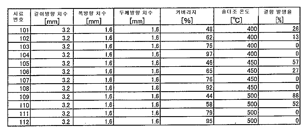
표 3으로부터, 내부전극의 커버리지가 75%이상인 조건을 만족하는 쪽이 결함 발생율의 저감에 보다 효과가 있는 것을 확인할 수 있다.It can be seen from Table 3 that the condition that the coverage of the internal electrode is 75% or more is more effective in reducing the defect occurrence rate.
즉, 표 3에 있어서, "결함 발생율"이 0%가 된 시료에 대하여, "커버리지"에 주목하면, "솔더조 온도"가 400℃일 때, "커버리지"가 75%이상이며, "결함 발생율"이 0%가 되고 있다. 이 점에서, 우선, 적어도 400℃의 열충격에 대해서는 "커버리지"가 75%이상인 것이 바람직한 것을 알 수 있다.That is, when the "solder bath temperature" is 400 ° C., the "coverage" is 75% or more, and the "defect occurrence rate" "Is 0%. From this point of view, it can be understood that the "coverage" is preferably 75% or more for a thermal shock of at least 400 ° C.
보다 고온의 열충격에 대해서는 "커버리지"가 보다 높은 것이 바람직하고, 보다 구체적으로는 "솔더조 온도"가 450℃일 때, "커버리지"가 76%이상이며, "결함 발생율"이 0%가 되고, "솔더조 온도"가 500℃일 때, "커버리지"가 79%이상이며, "결함 발생율"이 0%가 되고 있다.More specifically, when the "solder bath temperature" is 450 ° C, the "coverage" is 76% or more and the "defect occurrence rate" is 0% When the "solder bath temperature" is 500 ° C, the "coverage" is more than 79% and the "defect occurrence rate" is 0%.
1: 적층 세라믹 콘덴서 2: 적층체
3: 세라믹층 4, 5: 내부전극
6, 7: 주면 8, 9: 측면
10, 11: 단면1: Multilayer Ceramic Capacitor 2: Laminate
3: ceramic layer 4, 5: internal electrode
6, 7: Main surface 8, 9: Side
10, 11: Cross section
Claims (3)
상기 적층체는, 상기 세라믹층이 연장되는 방향으로 연장되면서 서로 대향하는 1쌍의 주면, 및 상기 적층체의 폭방향에서 서로 대향하는 1쌍의 측면 및 상기 적층체의 길이방향에서 서로 대향하는 1쌍의 단면을 가지며,
1쌍의 상기 측면 및 1쌍의 상기 단면은 상기 주면에 대하여 직교하는 방향으로 각각 연장되고,
상기 내부전극은, 1쌍의 상기 단면의 어느 한쪽으로까지 인출되고, 1쌍의 상기 측면의 각각에 대하여 폭방향 갭만큼 이격된 영역에 분포하고 있으면서, 1쌍의 상기 주면의 각각에 대하여 외층 두께만큼 이격된 영역에 분포하고 있는 적층 세라믹 전자부품으로서,
상기 내부전극의 두께가 0.4㎛이하라고 하는 제1의 조건과,
상기 폭방향 갭이 30㎛이하이며, 및 상기 외층 두께가 35㎛이하라고 하는 제2의 조건을 만족하는 것을 특징으로 하는 적층 세라믹 전자부품.And a laminate including a plurality of laminated ceramic layers and internal electrodes disposed between the ceramic layers,
Wherein the laminate includes a pair of main surfaces opposed to each other while extending in a direction in which the ceramic layer extends, a pair of side surfaces facing each other in the width direction of the laminate, and a pair of side surfaces facing each other in the longitudinal direction of the laminate A pair of cross-
A pair of the side surfaces and a pair of the end surfaces extend in a direction orthogonal to the main surface,
Wherein the internal electrode is extended to one of the pair of end faces and is distributed in a region spaced apart by a width direction gap with respect to each of the pair of side faces, Wherein the first and second ceramic electronic components are arranged in a region spaced apart from each other by a predetermined distance,
The first condition that the thickness of the internal electrode is 0.4 mu m or less,
The width direction gap is 30 占 퐉 or less, and the thickness of the outer layer is 35 占 퐉 or less.
또한 상기 내부전극의 커버리지가 75%이상이라고 하는 제3의 조건을 만족하는 것을 특징으로 하는 적층 세라믹 전자부품.3. The method of claim 2,
And a third condition that the coverage of the internal electrode is 75% or more.
Applications Claiming Priority (3)
| Application Number | Priority Date | Filing Date | Title |
|---|---|---|---|
| JP2010271097 | 2010-12-06 | ||
| JPJP-P-2010-271097 | 2010-12-06 | ||
| PCT/JP2011/077887 WO2012077585A1 (en) | 2010-12-06 | 2011-12-02 | Multilayer ceramic electronic component |
Related Child Applications (1)
| Application Number | Title | Priority Date | Filing Date |
|---|---|---|---|
| KR1020157001868A Division KR101589567B1 (en) | 2010-12-06 | 2011-12-02 | Multilayer ceramic electronic component, and method for manufacturing a multilayer ceramic electronic component |
Publications (2)
| Publication Number | Publication Date |
|---|---|
| KR20130087032A KR20130087032A (en) | 2013-08-05 |
| KR101541505B1 true KR101541505B1 (en) | 2015-08-03 |
Family
ID=46207074
Family Applications (2)
| Application Number | Title | Priority Date | Filing Date |
|---|---|---|---|
| KR1020157001868A KR101589567B1 (en) | 2010-12-06 | 2011-12-02 | Multilayer ceramic electronic component, and method for manufacturing a multilayer ceramic electronic component |
| KR1020137014554A KR101541505B1 (en) | 2010-12-06 | 2011-12-02 | Multilayer ceramic electronic component |
Family Applications Before (1)
| Application Number | Title | Priority Date | Filing Date |
|---|---|---|---|
| KR1020157001868A KR101589567B1 (en) | 2010-12-06 | 2011-12-02 | Multilayer ceramic electronic component, and method for manufacturing a multilayer ceramic electronic component |
Country Status (6)
| Country | Link |
|---|---|
| US (2) | US20130222972A1 (en) |
| JP (1) | JP5477479B2 (en) |
| KR (2) | KR101589567B1 (en) |
| CN (1) | CN103250217B (en) |
| TW (1) | TWI528392B (en) |
| WO (1) | WO2012077585A1 (en) |
Families Citing this family (22)
| Publication number | Priority date | Publication date | Assignee | Title |
|---|---|---|---|---|
| KR101771728B1 (en) * | 2012-07-20 | 2017-08-25 | 삼성전기주식회사 | Laminated ceramic electronic parts and fabricating method thereof |
| KR101922867B1 (en) * | 2012-10-12 | 2018-11-28 | 삼성전기 주식회사 | Multi-layered ceramic electronic component and method for manufacturing the same |
| KR101422938B1 (en) * | 2012-12-04 | 2014-07-23 | 삼성전기주식회사 | Embedded multilayer capacitor and method of manufacturing thereof, print circuit board having embedded multilayer capacitor |
| KR101462758B1 (en) * | 2013-01-29 | 2014-11-20 | 삼성전기주식회사 | Multilayer capacitor, method of manufacturing thereof and print circuit board having multilayer capacitor |
| KR101462785B1 (en) * | 2013-06-05 | 2014-11-20 | 삼성전기주식회사 | Multi-layered ceramic electronic component and method of manufacturing the same |
| KR101477405B1 (en) * | 2013-07-05 | 2014-12-29 | 삼성전기주식회사 | Multi-layered ceramic capacitor and mounting circuit board thereof |
| JP6015860B2 (en) * | 2013-07-17 | 2016-10-26 | 株式会社村田製作所 | Internal electrode paste |
| KR102078012B1 (en) * | 2014-01-10 | 2020-02-17 | 삼성전기주식회사 | Multi-layered ceramic capacitor and board having the same mounted thereon |
| JP2016040816A (en) * | 2014-08-13 | 2016-03-24 | 株式会社村田製作所 | Multilayer ceramic capacitor, multilayer ceramic capacitor couple including the same, and multilayer ceramic capacitor assembly |
| JP2016181597A (en) * | 2015-03-24 | 2016-10-13 | 太陽誘電株式会社 | Multilayer ceramic capacitor |
| JP6632808B2 (en) * | 2015-03-30 | 2020-01-22 | 太陽誘電株式会社 | Multilayer ceramic capacitors |
| CN106571229B (en) * | 2015-10-09 | 2018-11-09 | 株式会社村田制作所 | Electronic unit |
| JP2019102752A (en) | 2017-12-07 | 2019-06-24 | 太陽誘電株式会社 | Multilayer ceramic capacitor |
| JP7262181B2 (en) * | 2018-05-17 | 2023-04-21 | 太陽誘電株式会社 | Multilayer ceramic capacitor and manufacturing method thereof |
| US10971308B2 (en) * | 2018-07-20 | 2021-04-06 | Samsung Electro-Mechanics Co., Ltd | Multilayer capacitor |
| US11276526B2 (en) | 2018-08-29 | 2022-03-15 | Samsung Electro-Mechanics Co., Ltd. | Multilayer capacitor |
| JP7435947B2 (en) | 2018-08-29 | 2024-02-21 | サムソン エレクトロ-メカニックス カンパニーリミテッド. | stacked capacitor |
| KR102118495B1 (en) * | 2018-08-29 | 2020-06-09 | 삼성전기주식회사 | Multilayer capacitor |
| KR102126415B1 (en) * | 2018-08-29 | 2020-06-25 | 삼성전기주식회사 | Multilayer capacitor |
| KR20190116164A (en) * | 2019-09-02 | 2019-10-14 | 삼성전기주식회사 | Multi-layer ceramic electronic component |
| JP7432391B2 (en) * | 2020-02-28 | 2024-02-16 | 太陽誘電株式会社 | Ceramic electronic components and their manufacturing method |
| KR20220084603A (en) * | 2020-12-14 | 2022-06-21 | 삼성전기주식회사 | Multilayered capacitor and board for mounting the same |
Citations (3)
| Publication number | Priority date | Publication date | Assignee | Title |
|---|---|---|---|---|
| JP2000353636A (en) * | 1999-04-06 | 2000-12-19 | Matsushita Electric Ind Co Ltd | Laminated ceramic part |
| JP2003234242A (en) * | 2002-02-08 | 2003-08-22 | Murata Mfg Co Ltd | Laminated ceramic capacitor |
| US20070211404A1 (en) | 2006-03-10 | 2007-09-13 | Tdk Corporation | Laminated ceramic electronic component |
Family Cites Families (12)
| Publication number | Priority date | Publication date | Assignee | Title |
|---|---|---|---|---|
| JP3391268B2 (en) * | 1998-01-20 | 2003-03-31 | 株式会社村田製作所 | Dielectric ceramic and its manufacturing method, and multilayer ceramic electronic component and its manufacturing method |
| JP2000315621A (en) * | 1999-05-06 | 2000-11-14 | Murata Mfg Co Ltd | Laminated ceramic electronic parts |
| JP2001006971A (en) * | 1999-06-23 | 2001-01-12 | Philips Japan Ltd | Multilayered dielectric element |
| JP2001023852A (en) * | 1999-07-06 | 2001-01-26 | Murata Mfg Co Ltd | Laminated ceramic electronic component |
| CN1251259C (en) * | 1999-11-02 | 2006-04-12 | Tdk株式会社 | Multilayer capacitor |
| JP2005136132A (en) * | 2003-10-30 | 2005-05-26 | Tdk Corp | Laminated capacitor |
| JP2005259772A (en) * | 2004-03-09 | 2005-09-22 | Tdk Corp | Laminated ceramic capacitor |
| JP2005167290A (en) * | 2005-03-11 | 2005-06-23 | Murata Mfg Co Ltd | Method of manufacturing laminated ceramic electronic component |
| CN101517672B (en) * | 2006-09-27 | 2012-05-16 | 京瓷株式会社 | Multilayer ceramic capacitor and method for production thereof |
| JP2008091400A (en) * | 2006-09-29 | 2008-04-17 | Tdk Corp | Laminated ceramic capacitor and its manufacturing method |
| WO2010013414A1 (en) * | 2008-07-29 | 2010-02-04 | 株式会社村田製作所 | Laminated ceramic capacitor |
| CN103443050B (en) * | 2011-03-16 | 2016-09-28 | 株式会社村田制作所 | Dielectric ceramics and laminated ceramic capacitor |
-
2011
- 2011-12-02 WO PCT/JP2011/077887 patent/WO2012077585A1/en active Application Filing
- 2011-12-02 CN CN201180058768.9A patent/CN103250217B/en active Active
- 2011-12-02 KR KR1020157001868A patent/KR101589567B1/en active IP Right Grant
- 2011-12-02 JP JP2012547817A patent/JP5477479B2/en active Active
- 2011-12-02 KR KR1020137014554A patent/KR101541505B1/en active IP Right Grant
- 2011-12-06 TW TW100144931A patent/TWI528392B/en active
-
2013
- 2013-04-04 US US13/856,475 patent/US20130222972A1/en not_active Abandoned
-
2016
- 2016-06-03 US US15/172,199 patent/US9972438B2/en active Active
Patent Citations (3)
| Publication number | Priority date | Publication date | Assignee | Title |
|---|---|---|---|---|
| JP2000353636A (en) * | 1999-04-06 | 2000-12-19 | Matsushita Electric Ind Co Ltd | Laminated ceramic part |
| JP2003234242A (en) * | 2002-02-08 | 2003-08-22 | Murata Mfg Co Ltd | Laminated ceramic capacitor |
| US20070211404A1 (en) | 2006-03-10 | 2007-09-13 | Tdk Corporation | Laminated ceramic electronic component |
Also Published As
| Publication number | Publication date |
|---|---|
| JPWO2012077585A1 (en) | 2014-05-19 |
| CN103250217A (en) | 2013-08-14 |
| US20130222972A1 (en) | 2013-08-29 |
| WO2012077585A1 (en) | 2012-06-14 |
| US20160284474A1 (en) | 2016-09-29 |
| TW201232576A (en) | 2012-08-01 |
| CN103250217B (en) | 2017-07-18 |
| KR20150027244A (en) | 2015-03-11 |
| JP5477479B2 (en) | 2014-04-23 |
| TWI528392B (en) | 2016-04-01 |
| KR101589567B1 (en) | 2016-01-29 |
| KR20130087032A (en) | 2013-08-05 |
| US9972438B2 (en) | 2018-05-15 |
Similar Documents
| Publication | Publication Date | Title |
|---|---|---|
| KR101541505B1 (en) | Multilayer ceramic electronic component | |
| JP5271377B2 (en) | Multilayer ceramic capacitor | |
| JP6812477B2 (en) | Multilayer ceramic capacitors, manufacturing methods for multilayer ceramic capacitors, and mounting boards for multilayer ceramic capacitors | |
| JP5313289B2 (en) | Multilayer ceramic capacitor | |
| JP5206440B2 (en) | Ceramic electronic components | |
| JP2008091400A (en) | Laminated ceramic capacitor and its manufacturing method | |
| WO2006126562A1 (en) | Multilayer ceramic electronic component | |
| JP2006186316A (en) | Ceramic electronic component and laminated ceramic capacitor | |
| US10418180B2 (en) | Electronic component and manufacturing method for the same | |
| KR20120133716A (en) | Multilayer ceramic capacitor | |
| JP2018067568A (en) | Method of manufacturing multilayer ceramic capacitor | |
| JP5852321B2 (en) | Multilayer ceramic capacitor | |
| US10504652B2 (en) | Electronic component | |
| KR101950715B1 (en) | Multilayer ceramic capacitor | |
| JP2012151175A (en) | Ceramic electronic component, ceramic electronic component mounting structure, and ceramic electronic component manufacturing method | |
| JP2007123389A (en) | Laminated electronic component | |
| JP2005159121A (en) | Laminated ceramic electronic component | |
| JP6110927B2 (en) | Multilayer ceramic capacitor | |
| JP4175284B2 (en) | Manufacturing method of multilayer ceramic electronic component | |
| JP2022073617A (en) | Multilayer ceramic capacitor | |
| JP2011165935A (en) | Laminated electronic component | |
| JP2006128282A (en) | Laminated electronic component and its manufacturing method | |
| JP2013021010A (en) | Multilayer ceramic capacitor | |
| JP2005032807A (en) | Lamination ceramic electronic component and its method for manufacturing | |
| KR20150105690A (en) | Multilayered ceramic electronic component |
Legal Events
| Date | Code | Title | Description |
|---|---|---|---|
| A201 | Request for examination | ||
| E902 | Notification of reason for refusal | ||
| AMND | Amendment | ||
| E601 | Decision to refuse application | ||
| A107 | Divisional application of patent | ||
| AMND | Amendment | ||
| E902 | Notification of reason for refusal | ||
| X701 | Decision to grant (after re-examination) | ||
| GRNT | Written decision to grant | ||
| FPAY | Annual fee payment |
Payment date: 20180719 Year of fee payment: 4 |