KR101148918B1 - Porous underlayer film and underlayer film forming composition used for forming the same - Google Patents
Porous underlayer film and underlayer film forming composition used for forming the same Download PDFInfo
- Publication number
- KR101148918B1 KR101148918B1 KR1020057019677A KR20057019677A KR101148918B1 KR 101148918 B1 KR101148918 B1 KR 101148918B1 KR 1020057019677 A KR1020057019677 A KR 1020057019677A KR 20057019677 A KR20057019677 A KR 20057019677A KR 101148918 B1 KR101148918 B1 KR 101148918B1
- Authority
- KR
- South Korea
- Prior art keywords
- underlayer film
- photoresist
- porous
- polymer
- forming composition
- Prior art date
Links
Images

Classifications
-
- G—PHYSICS
- G03—PHOTOGRAPHY; CINEMATOGRAPHY; ANALOGOUS TECHNIQUES USING WAVES OTHER THAN OPTICAL WAVES; ELECTROGRAPHY; HOLOGRAPHY
- G03F—PHOTOMECHANICAL PRODUCTION OF TEXTURED OR PATTERNED SURFACES, e.g. FOR PRINTING, FOR PROCESSING OF SEMICONDUCTOR DEVICES; MATERIALS THEREFOR; ORIGINALS THEREFOR; APPARATUS SPECIALLY ADAPTED THEREFOR
- G03F7/00—Photomechanical, e.g. photolithographic, production of textured or patterned surfaces, e.g. printing surfaces; Materials therefor, e.g. comprising photoresists; Apparatus specially adapted therefor
- G03F7/004—Photosensitive materials
- G03F7/09—Photosensitive materials characterised by structural details, e.g. supports, auxiliary layers
- G03F7/11—Photosensitive materials characterised by structural details, e.g. supports, auxiliary layers having cover layers or intermediate layers, e.g. subbing layers
Abstract
포토 레지스트 층과 인터믹싱이 일어나지 않고, 포토 레지스트에 비교하여 큰 드라이에칭 속도를 가지는, 반도체장치 제조의 리소그라피 프로세스에 사용되는 하층막을 제공한다. 구체적으로는, 발포제, 유기재료 및 용제를 포함하거나, 또는, 발포성기를 가지는 폴리머 및 용제를 포함하는, 반도체장치의 제조에 사용되는 다공질 하층막을 형성하기 위한 하층막 형성 조성물. 이 조성물로 형성되는 하층막은, 그 내부에 공공을 가지는 다공질 구조로 이루어지고, 큰 드라이에칭 속도의 달성이 가능하다.Provided is an underlayer film used in the lithography process of semiconductor device manufacture, which does not intermix with the photoresist layer and has a large dry etching rate compared to the photoresist. Specifically, an underlayer film-forming composition for forming a porous underlayer film for use in the manufacture of a semiconductor device containing a foaming agent, an organic material and a solvent, or a polymer and a solvent having a foamable group. The underlayer film formed of this composition consists of a porous structure which has a cavity inside, and can achieve a large dry etching rate.
포토 레지스트, 리소그라피, 다공질 하층막, 발포제, 발포성기 Photoresist, Lithography, Porous Underlayer, Foaming Agent, Foaming Machine
Description
본 발명은, 반도체 기판과 포토 지스트의 사이에 다공질 하층막을 형성하는 것을 포함하는, 반도체 장치의 제조에 이용되는 포토 레지스트 패턴의 형성방법에 관한 것이다.This invention relates to the formation method of the photoresist pattern used for manufacture of a semiconductor device including forming a porous underlayer film between a semiconductor substrate and a photoresist.
또한, 본 발명은, 반도체 장치의 제조에 이용되는 포토 레지스트 패턴의 형성에 사용되는 다공질 하층막을 형성하기 위한 하층막 형성 조성물에 관한 것이고, 그리고, 이 하층막 형성 조성물을 이용한 다공질 하층막의 형성방법, 및 이 하층막 형성조성물로 형성되는 다공질 하층막에 관한 것이다.Moreover, this invention relates to the underlayer film forming composition for forming the porous underlayer film used for formation of the photoresist pattern used for manufacture of a semiconductor device, and the formation method of the porous underlayer film using this underlayer film forming composition, And a porous underlayer film formed from the underlayer film formation composition.
종래부터 반도체 장치의 제조에 있어서, 포토 레지스트를 이용한 리소그라피에 의한 미세가공이 행해지고 있다. 이 미세가공은 실리콘 웨이퍼 등의 반도체 기판상에 포토 레지스트의 박막을 형성하고, 그 위에 반도체 디바이스의 패턴이 그려진 마스크 패턴을 통하여 자외선 등의 활성광선을 조사하고, 현상하여, 얻어진 포토 레지스트 패턴을 보호막으로 하여 기판을 에칭처리 함으로써, 기판 표면에 상기 패턴에 대응하는 미세 요철을 형성하는 가공법이다. 그런데, 근년, 반도체 디바이스의 고집적도화가 진행하고, 사용되는 활성광선도 KrF 액시머 레이저(248nm)로부터 ArF 액시머 레이저(193nm)로 단파장화 되는 경향이다. 이것에 수반한 활성광선의 기판으로부터의 난반사나 정상파의 영향이 큰 문제로 되었다. 여기서, 이 문제를 해결하기 위하여, 포토 레지스트와 기판 사이에 반사방지막(Bottom Anti-Reflective Coating, BARC)를 설치하는 방법이 널리 검토되고 있다. 이러한 반사방지막으로는, 그 사용의 용이함 등으로 인하여, 흡광성 물질과 고분자 화합물 등으로 이루어진 유기 반사 방지막에 관하여 수많은 검토가 행해지고 있고, 예를 들면, 가교반응기인 히드록실기와 흡광기를 동일분자내에 가지는 아크릴 수지형 반사 방지막이나 가교반응기인 히드록실기와 흡광기를 동일 분자내에 가지는 노보락 수지형 반사 방지막 등을 들 수 있다(예를 들면, 특허문헌 1, 특허문헌 2 참조).Background Art Conventionally, in manufacturing semiconductor devices, fine processing by lithography using photoresist has been performed. This microfabrication forms a thin film of photoresist on a semiconductor substrate such as a silicon wafer, irradiates active light such as ultraviolet rays through a mask pattern on which a pattern of a semiconductor device is drawn thereon, and develops the photoresist pattern thus obtained. It is a processing method of forming the fine unevenness | corrugation corresponding to the said pattern on the surface of a board | substrate by etching a board | substrate. By the way, in recent years, the high density of semiconductor devices advances, and the actinic light used also tends to become short wavelength from KrF aximmer laser (248 nm) to ArF aximmer laser (193 nm). The influence of diffuse reflection and standing waves of the actinic light accompanying this became a big problem. In order to solve this problem, a method of providing a bottom anti-reflective coating (BARC) between the photoresist and the substrate has been widely studied. As such an antireflection film, due to its ease of use and the like, a number of studies have been conducted on an organic antireflection film made of a light absorbing substance, a polymer compound, and the like. For example, a hydroxyl group and a light absorber, which are crosslinking reaction groups, are formed in the same molecule. Examples thereof include an acrylic resin antireflection film and a novolak resin antireflection film having a hydroxyl group and a light absorber in the same molecule as the crosslinking reaction group (see, for example,
유기 반사 방지막에 요구되는 특성으로는, 빛이나 방사선에 대하여 큰 흡광도를 가지는 것, 포토 레지스트 층과 인터 믹싱이 일어나지 않는 것(포토 레지스트 용제에 불용(不溶)인 것), 가열 소성시에 반사 방지막으로부터 상층 포토 레지스트로의 저분자 물질의 확산이 일어나지 않는 것, 포토 레지스트에 비하여 큰 드라이 에칭 속도를 가지는 것 등이 있다(예를 들면, 비특허문헌 1, 비특허문헌 2, 비특허문헌 3 참조).The characteristics required for the organic antireflection film include those having a large absorbance with respect to light or radiation, no intermixing with the photoresist layer (insoluble in photoresist solvent), and an antireflection film during heating and baking. Diffusion of a low molecular weight material from the photoresist to the upper photoresist, and a larger dry etching rate than the photoresist (for example, see Non-Patent
또한, 근년, 반도체장치의 패턴 룰의 미세화에 따라 밝혀진 배선지연의 문제를 해결하기 위해, 배선재료로서 구리를 사용하는 검토가 행해지고 있다. 그리고, 그것과 함께 반도체기판으로의 배선형성 방법으로서 듀얼 다마신 프로세스의 검토가 행해지고 있다. 듀얼 다마신 프로세스는 비어 홀이 형성되고, 큰 아스팩트 (aspect) 비를 가지는 기판에 대하여 반사 방지막이 형성되는 것으로 이루어진다. 그 때문에, 이 프로세스에 사용되는 반사 방지막에 대해서는, 홀을 극간(隙間) 없이 충전할 수 있는 매입특성이나, 기판 표면에 평탄한 막이 형성되도록 되는 평탄화 특성이 요구되고 있다.Moreover, in recent years, in order to solve the problem of the wiring delay discovered by the refinement | miniaturization of the pattern rule of a semiconductor device, the examination which uses copper as a wiring material is performed. In addition, the dual damascene process is examined as a wiring formation method to a semiconductor substrate. The dual damascene process consists of a via hole being formed and an antireflective film formed on the substrate having a large aspect ratio. Therefore, for the anti-reflection film used in this process, embedding characteristics in which holes can be filled without gaps, and planarization characteristics such that a flat film is formed on the substrate surface are required.
그러나, 유기계 반사 방지막용 재료를 큰 아스팩트 비를 가지는 기판에 적용하는 것은 어렵고, 근년, 매립특성이나 평탄화특성에 중점을 둔 재료가 개발되어 오고 있었다(예를 들면, 특허문헌 3, 특허문헌 4, 특허문헌 5, 특허문헌 6 참조).However, it is difficult to apply the organic antireflection film material to a substrate having a large aspect ratio, and in recent years, materials have been developed that focus on embedding characteristics and planarization characteristics (for example, Patent Documents 3 and 4). , Patent Document 5, Patent Document 6).
또한, 반도체 등의 디바이스 제조에 있어서, 유전체층에 의한 포토 레지스트 층의 포이즈닝 효과를 감소시키기 위해, 가교가능한 폴리머 등을 포함하는 조성물로 형성되는 배리어 층을, 유전체층과 포토레지스트 층의 사이에 설치한다고 하는 방법이 개시되어 있다(예를 들면, 특허문헌 7 참조).In addition, in the manufacture of devices such as semiconductors, in order to reduce the poisoning effect of the photoresist layer by the dielectric layer, a barrier layer formed of a composition containing a crosslinkable polymer or the like is provided between the dielectric layer and the photoresist layer. The method of making is disclosed (for example, refer patent document 7).
이러하듯이, 근년의 반도체 장치의 제조에는, 반사 방지 효과를 시작으로, 여러가지 효과를 달성하기 위해, 반도체 기판과 포토 레지스트의 사이, 즉 포토레지스트의 하층으로, 유기화합물을 포함하는 조성물로 형성된 유기계의 하층막이 배치되도록 되어 왔다.As described above, in recent years, in the manufacture of semiconductor devices, in order to achieve various effects, including an antireflection effect, an organic system formed of a composition containing an organic compound between a semiconductor substrate and a photoresist, that is, a lower layer of the photoresist, is achieved. Underlayer films have been arranged.
그런데, 그러한 하층막은, 포토 레지스트와 비교하여 큰 드라이 에칭 속도를 가질 필요가 있다. 반도체 기판의 가공은, 패턴이 형성된 포토 레지스트를 보호막으로 드라이 에칭에 의해 이루어지지만, 그 때, 기판에 앞서, 우선, 포토 레지스트를 보호막으로 드라이 에칭에 의한 하층막의 제거가 행해진다. 그 때문에, 하층막의 제거시에도 포토 레지스트 막두께의 감소가 일어난다. 그리고, 하층막의 제거 에 긴 시간을 요하는 것이라면, 포토 레지스트 막두께의 감소량이 크게 되고, 기판의 가공에 필요한 막두께를 확보할 수 없게 된다고 하는 문제가 발생한다. 특히, 근년, 포토 레지스트 패턴의 선폭의 미세화에 수반하여, 포토 레지스트의 도괴(倒壞) 등을 방지하기 위해 포토 레지스트의 박막화가 요망되어 지고 있다. 그 때문에, 종래보다도 많이, 단시간으로 제거가능한 하층막, 즉, 큰 드라이 에칭 속도를 가지는 하층막이 요구되어지고 있다.By the way, such an underlayer film needs to have a large dry etching rate compared with a photoresist. Although processing of a semiconductor substrate is performed by dry etching the photoresist in which the pattern was formed by the protective film, at that time, prior to a board | substrate, the underlayer film | membrane is removed by dry etching first with a photoresist as a protective film. Therefore, the thickness of the photoresist film also occurs when the underlayer film is removed. If the removal of the underlayer film requires a long time, the amount of reduction in the photoresist film thickness becomes large, resulting in a problem that the film thickness necessary for processing the substrate cannot be secured. In particular, in recent years, with the miniaturization of the line width of a photoresist pattern, in order to prevent collapse of a photoresist, etc., the thinning of the photoresist is desired. For this reason, there is a demand for a lower layer film that can be removed in a shorter time than conventionally, that is, a lower layer film having a large dry etching rate.
특허문헌 1 : 미국특허 제5919599호 명세서Patent Document 1: US Patent No. 5919599
특허문헌 2 : 미국특허 제5693691호 명세서Patent Document 2: US Patent No. 5693691
특허문헌 3 : 특개 2000-294504호 공보Patent Document 3: Japanese Patent Application Laid-Open No. 2000-294504
특허문헌 4 : 특개 2002-47430호 공보Patent Document 4: Japanese Patent Application Laid-Open No. 2002-47430
특허문헌 5 : 특개 2002-190519호 공보Patent Document 5: Japanese Patent Application Laid-Open No. 2002-190519
특허문헌 6 : 국제공개 제02/05035호 팜플렛Patent Document 6: International Publication No. 02/05035 Pamphlet
특허문헌 7 : 특개 2002-128847호 공보Patent Document 7: Japanese Patent Application Laid-Open No. 2002-128847
비특허문헌 1 : 톰?린치(Tom Lynch)외 3명, 「프로퍼티 앤드 퍼포먼스 오브 니어 UV 리플렉티비티 콘트롤 레이어(Properties and Performance of Near UV Reflectivity Control Layers)」, (미국), 인 어드밴스 인 레지스트 테크놀로지 앤드 프로세싱 XI(in Advances in Resist Technology and Processing XI), 옴카람?나라마스(Omkaram Nalamasu) 편, 프로시딩즈 오브 에스피아이이(Proceedings of SPIE), 1994년, 제2195권(Vol. 2195), p. 225-229[Non-Patent Document 1] Tom Lynch et al., 3, `` Properties and Performance of Near UV Reflectivity Control Layers, '' (US), In Advance In resist In Advances in Resist Technology and Processing XI, by Omkaram Nalamasu, Proceedings of SPIE, 1994, Vol. 2195, Vol. 2195, p. . 225-229
비특허문헌 2 : 지?테일러(G. Taylor)외 13명, 「메타크릴레이트 레지스트 앤드 안티리플렉티브 코팅 포 193nm 리소그라피(Methacrylate Resist and Antireflective Coatings for 193nm Lithography)」, (미국), 인 마이크로리소그라피 1999 : 어드밴스 인 레지스트 테크놀로지 앤드 프로세싱 XVI(in Microlithography 1999 : Advances in Resist Technology and Processing XVI), 윌?콘레이(Will Conley) 편, 프로시딩즈 오브 에스피아이이(Proceedings of SPIE), 1999년, 제3678권(Vol. 3678), p. 174-185[Non-Patent Document 2] G. Taylor et al., 13, `` Methacrylate Resist and Antireflective Coatings for 193nm Lithography '', (US), Phosphorus Microlithography 1999: In Microlithography 1999: Advances in Resist Technology and Processing XVI, Will Conley, Proceedings of SPIE, 1999, vol. 3678 (Vol. 3678), p. 174-185
비특허문헌 3 : 짐?디?메더(Jim D. Meador) 외 6명, 「리선트 프로그레스 인 193nm 안티리플렉티브 코팅스(Recent Progress in 193nm Antireflective Coatings)」, (미국), 인 마이크로리소그라피 1999 : 어드밴스 인 레지스트 테크놀로지 앤드 프로세싱 XVI(in Microlithography 1999 : Advances in Resist Technology and Processing XVI), 윌?콘레이(Will Conley) 편, 프로시딩즈 오브 에스피아이이(Proceedings of SPIE), 1999년, 제3678권(Vol. 3678), p. 800-809[Non-Patent Document 3] Jim D. Meador, et al., 6, `` Recent Progress in 193nm Antireflective Coatings, '' (US), In Microlithography 1999: In Microlithography 1999: Advances in Resist Technology and Processing XVI, Will Conley, Proceedings of SPIE, 1999, vol. 3678 (Vol. 3678), p. 800-809
이러한 현상에 착안하여 본발명자등은 예의 연구를 행한 결과, 하층막을 공공(空孔)을 가진 막, 즉, 다공질 하층막으로 함으로써, 그, 드라이 에칭에 의한 제거 속도를 높일 수가 있다는 것을 도출하고, 본발명을 완성한 것이다.In light of these phenomena, the present inventors have made a thorough study. As a result, the lower layer film is made of a hollow layer, that is, a porous lower layer film, and thus, the removal rate by dry etching can be derived. The present invention has been completed.
즉, 본 발명의 목적은, 큰 드라이 에칭 속도를 가지는 다공질 하층막을 반도체 기판상에 형성하는 것을 포함하는, 반도체 장치의 제조에 이용되는 포토 레지스트 패턴의 형성방법을 제공하는 것이다.That is, an object of the present invention is to provide a method of forming a photoresist pattern used in the manufacture of a semiconductor device, comprising forming a porous underlayer film having a large dry etching rate on a semiconductor substrate.
또한, 본 발명의 목적은, 다공질 하층막의 형성에 사용되는 하층막형성 조성물을 제공하는 것에 있고, 또한, 이 조성물로 형성되는 다공질 하층막, 및 이 조성물을 이용한 다공질 하층막의 형성방법을 제공하는 것에 있다.Moreover, the objective of this invention is providing the underlayer film forming composition used for formation of a porous underlayer film, and providing the porous underlayer film formed from this composition, and the method of forming a porous underlayer film using this composition. have.
본 발명은, 제 1 관점으로서, 반도체 기판상에 다공질 하층막을 형성하는 공정, 이 다공질 하층막 위에 포토 레지스트 층을 형성하는 공정, 상기 다공질 하층막과 상기 포토 레지스트 피복된 반도체 기판을 노광하는 공정, 상기 노광후에 상기 포토 레지스트를 현상하는 공정, 및 상기 포토 레지스트가 현상 제거된 부분의 다공질 하층막을 에칭에 의해 제거하는 공정, 을 포함하는, 반도체 장치의 제조에 이용되는 포토 레지스트 패턴의 형성방법,According to a first aspect of the present invention, there is provided a process for forming a porous underlayer film on a semiconductor substrate, a step of forming a photoresist layer on the porous underlayer film, a step of exposing the porous underlayer film and the photoresist coated semiconductor substrate, Developing the photoresist after the exposure; and removing the porous underlayer film of the portion from which the photoresist has been removed by etching, the method of forming a photoresist pattern used in the manufacture of a semiconductor device;
제 2 관점으로, 상기 반도체 기판상에 다공질 하층막을 형성하는 공정의 앞 또는 뒤에, 반사 방지막 또는 평탄화 막을 형성하는 공정을 추가로 포함하는, 제 1 관점에 기재된 포토 레지스트 패턴의 형성방법,In a second aspect, the method of forming the photoresist pattern according to the first aspect, further comprising a step of forming an antireflection film or a planarization film before or after the step of forming the porous underlayer film on the semiconductor substrate,
제 3 관점으로서, 상기 다공질 하층막이, 반도체 기판상에 발포제 또는 발포성 기를 가지는 폴리머를 포함하는 하층막 형성 조성물을 도포하고, 가열함으로써 형성된 것인 제 1 관점에 기재된 포토 레지스트 패턴의 형성방법,As a 3rd viewpoint, the said porous underlayer film is formed by apply | coating the underlayer film forming composition containing a foaming agent or a polymer which has a foamable group, and heating it on the semiconductor substrate, The formation method of the photoresist pattern as described in a 1st viewpoint.
제 4 관점으로서, 발포제, 유기재료 및 용제를 포함하는, 반도체 장치의 제조에 사용되는 다공질 하층막을 형성하기 위한 하층막 형성 조성물,As a 4th viewpoint, the underlayer film forming composition for forming the porous underlayer film used for manufacture of a semiconductor device containing a foaming agent, an organic material, and a solvent,
제 5 관점으로서, 발포성 기를 가지는 폴리머 및 용제를 포함하는, 반도체 장치의 제조에 사용되는 다공질 하층막을 형성하기 위한 하층막 형성 조성물,As a 5th viewpoint, the underlayer film formation composition for forming the porous underlayer film used for manufacture of a semiconductor device containing the polymer and solvent which have a foamable group,
제 6 관점으로서, 발포성 기를 가지는 폴리머, 유기재료 및 용제를 포함하는, 반도체 장치의 제조에 사용되는 다공질 하층막을 형성하기 위한 하층막 형성 조성물,As a sixth aspect, an underlayer film forming composition for forming a porous underlayer film for use in the manufacture of a semiconductor device, comprising a polymer having an expandable group, an organic material, and a solvent,
제 7 관점으로서, 상기 발포제가, 가열에 의해 분해하여 질소, 이산화탄소 또는 수증기를 발생하는 것인 제 4 관점에 기재된 하층막 형성 조성물,As a seventh aspect, the underlayer film forming composition according to the fourth aspect, wherein the blowing agent is decomposed by heating to generate nitrogen, carbon dioxide, or water vapor;
제 8 관점으로서, 상기 발포성 기를 가지는 폴리머가, 가열에 의해 분해하여 질소, 이산화탄소 또는 수증기를 발생하는 것인 제 5 관점 또는 제 6 관점에 기재된 하층막 형성 조성물,As an eighth aspect, the underlayer film forming composition according to the fifth or sixth aspect, wherein the polymer having the expandable group decomposes by heating to generate nitrogen, carbon dioxide, or water vapor;
제 9 관점으로서, 상기 유기재료가, 폴리머, 가교성 화합물 및 흡광성 화합물로 이루어진 군에서 선택된 적어도 1개의 성분을 포함하는 것인 제 4 관점 또는 제 6관점에 기재된 하층막 형성 조성물,As a ninth aspect, the underlayer film forming composition according to the fourth aspect or the sixth aspect, wherein the organic material includes at least one component selected from the group consisting of a polymer, a crosslinkable compound, and a light absorbing compound,
제 10 관점으로서, 상기 폴리머가, 벤젠 고리, 나프탈렌 고리, 안트라센 고리 및 트리아진 고리로 이루어진 군에서 선택된 적어도 1개의 방향 고리 구조를 가지는 것인 제 9 관점에 기재된 하층막 형성 조성물,As a tenth aspect, the underlayer film forming composition according to the ninth aspect, wherein the polymer has at least one aromatic ring structure selected from the group consisting of a benzene ring, a naphthalene ring, an anthracene ring, and a triazine ring,
제 11 관점으로서, 상기 가교성 화합물이, 적어도 2개의 가교 형성 치환기를 가지는 것인 제 9 관점에 기재된 하층막 형성 조성물,As an eleventh aspect, the underlayer film forming composition according to the ninth aspect, wherein the crosslinkable compound has at least two crosslinking substituents,
제 12 관점으로서, 상기 흡광성 화합물이, 벤젠 고리, 나프탈렌 고리, 안트라센 고리 및 트리아진 트리온 고리로 이루어진 그룹에서 선택된 적어도 1개의 고리 구조를 가지는 것인 제 9 관점에 기재된 하층막 형성 조성물,As a twelfth aspect, the underlayer film forming composition according to the ninth aspect, wherein the light absorbing compound has at least one ring structure selected from the group consisting of a benzene ring, a naphthalene ring, an anthracene ring, and a triazine trion ring,
제 13 관점으로서, 제 4 관점 내지 제 12 관점 중 어느 하나에 기재된 하층막 형성 조성물을 기판 위에 도포하고, 가열하여 다공질 하층막을 형성하는 공정, 이 다공질 하층막에 포토 레지스트 층을 형성하는 공정, 상기 다공질 하층막과 상기 포토 레지스트로 피복된 반도체 기판을 노광하는 공정, 상기 노광후에 상기 포토 레지스트를 현상하는 공정, 및 상기 포토 레지스트가 현상제거된 부분의 다공질 하층막을 에칭에 의해 제거하는 공정,을 포함하는 반도체 장치의 제조에 이용되는 포토 레지스트 패턴의 형성방법, 이다.13th viewpoint WHEREIN: The process of apply | coating the underlayer film forming composition in any one of a 4th viewpoint thru | or a 12th viewpoint on a board | substrate, and heating to form a porous underlayer film, The process of forming a photoresist layer in this porous underlayer film, The said Exposing the porous underlayer film and the semiconductor substrate coated with the photoresist, developing the photoresist after the exposure, and removing the porous underlayer film of the portion where the photoresist has been removed by etching; And a method of forming a photoresist pattern used in the manufacture of a semiconductor device.
본 발명은, 이러한 구성에 의해, 포토 레지스트와 인터 믹싱을 일으키지 않고, 큰 드라이 에칭 속도를 가지는 다공질 하층막을 제공할 수 있다.The present invention can provide a porous underlayer film having a large dry etching rate without causing intermixing with the photoresist.
얻어진 다공질 하층막은, 드라이 에칭 프로세스에서 신속한 제거가 가능하기 때문에, 반도체 기판 가공시에 보호막으로 기능하는 포토 레지스트의 막두께의 감소량을 저감하는 것이 가능하게 된다.Since the obtained porous underlayer film can be removed quickly by a dry etching process, it becomes possible to reduce the amount of reduction of the film thickness of the photoresist which functions as a protective film at the time of processing a semiconductor substrate.
또한, 본 발명의 방법에 의해, 초기의 포토 레지스트의 막두께가 적은 경우에도, 반도체 기판의 가공에 필요한, 패턴화된 포토 레지스트 및 하층막으로 이루어진 보호막의 확보가 가능하게 된다.In addition, according to the method of the present invention, even if the film thickness of the initial photoresist is small, it is possible to secure a protective film made of a patterned photoresist and an underlayer film required for processing the semiconductor substrate.
도 1은, 본 발명의 다공질 하층막을 사용한 제조 프로세스에서의 반도체 기판의 포토 레지스트 패턴의 단면구조를 나타내는 그림이고, 도면 중의 부호 (11)은 반도체 기판을 나타내고, (12)는 다공질 하층막을 나타내며, (13)은 포토 레지스트 를 나타내고, (14)는 다공질이 아닌 하층막을 나타내며, (15), (16)은 포토 레지스트의 막두께의 감소부분을 나타낸다.1 is a diagram showing a cross-sectional structure of a photoresist pattern of a semiconductor substrate in a manufacturing process using the porous underlayer film of the present invention,
본 발명은, 공공(空孔)을 가지는 하층막, 즉, 다공질 하층막이 큰 에칭 속도를 가지는 것을 발견한 것에 기초하고 있다.The present invention is based on the finding that an underlayer film having a void, that is, a porous underlayer film has a large etching rate.
본 발명은, 다공질 하층막을 사용한 반도체 장치의 제조에 사용되는 포토 레지스트 패턴의 형성방법, 다공질 하층막의 형성에 사용되는 하층막 형성 조성물, 및, 이 하층막 형성 조성물을 이용한 다공질 하층막의 형성방법을 제공하는 것에 관한 것이다.This invention provides the formation method of the photoresist pattern used for manufacture of the semiconductor device using a porous underlayer film, the underlayer film forming composition used for formation of a porous underlayer film, and the formation method of the porous underlayer film using this underlayer film forming composition. It's about doing.
본 발명의 포토 레지스트 패턴의 형성방법에 있어서는, 반도체 기판상에 다공질 하층막이 형성된 후, 그 다공질 하층막 상에 포토 레지스트 칭이 형성된다. 여기서 다공질 하층막의 막두께로서는, 예를 들면 30~2000nm 이고, 또는 30~1500nm 이며, 또한, 예를 들면, 50~1500nm 이다. 포토 레지스트 층의 막두께로서는, 예를 들면 50~10000nm 이고, 또는 50~8000nm 이며, 또한, 예를 들면, 100~5000nm 이다.In the method of forming the photoresist pattern of the present invention, after the porous underlayer film is formed on the semiconductor substrate, photoresisting is formed on the porous underlayer film. Here, as a film thickness of a porous underlayer film, it is 30-2000 nm, or 30-1500 nm, for example, 50-1500 nm. As a film thickness of a photoresist layer, it is 50-10000 nm, or 50-8000 nm, for example, and is 100-5000 nm, for example.
다공질 하층막에 있어서, 그 막에 점하는 공공의 비율로서는, 그 체적으로서, 예를 들면, 5~80% 이고, 또는, 10~50% 이며, 또한, 10~30% 이다. 공공의 비율이 이것보다 크게 되면, 균일한 막의 형성이 곤란하게 된다. 또한, 공공의 크기로서는, 공공 직경으로, 예를 들면 1~500nm 이고, 또는, 1~50nm이다. 공공이 이것보다 크게 되면, 상층의 포토 레지스트의 패턴 형성에 악영향을 미치게 된다.In the porous underlayer film, the proportion of the pores occupying the film is, for example, 5 to 80%, or 10 to 50%, and 10 to 30% as the volume. If the proportion of the pores is larger than this, formation of a uniform film becomes difficult. In addition, as a pore size, it is 1-500 nm or 1-50 nm in a pore diameter, for example. If the void becomes larger than this, it will adversely affect the pattern formation of the upper photoresist.
다음으로, 다공질 하층막과 포토 레지스트 층으로 피복된 반도체 기판이, 미 리 설정된 마스크를 통하여, i선, KrF 액시머 레이저, ArF 액시머 레이저 등의 빛으로 노광된다. 노광후, 필요에 띠라 노광후 가열(PEB, post exposure bake)을 행한다. 그리고, 알칼리성 수용액 등을 사용한 현상에 의해, 설정된 패턴에 따른 포토 레지스트가 부분적으로 제거된다(도 1의 (A)). 도 1의 (A)에서 (11)은 반도체 기판, (12)는 다공질 하층막, (13)은 패턴화된 포토 레지스트,이다. 또한, 도 1의 (B)는 다공질이 아닌 하층막 (14)를 사용하여, 동일한 공정에 의해 형성된 포토 레지스트를 나타내는 도면이다.Next, the semiconductor substrate coated with the porous underlayer film and the photoresist layer is exposed to light such as an i-line, a KrF aximmer laser, an ArF aximmer laser, or the like through a preset mask. After exposure, post-exposure bake (PEB) is performed as needed. And the photoresist according to the set pattern is partially removed by image development using alkaline aqueous solution etc. (FIG.1 (A)). 1A to 11A are semiconductor substrates, 12 is a porous underlayer film, and 13 is a patterned photoresist. 1B is a diagram showing a photoresist formed by the same process using the
이어서, 포토 레지스트가 제거된 부분의 하층막을 에칭에 의해 제거하고, 반도체 기판을 노출시킨다(도 1의 (C) 및 (D)는, (A) 및 (B)에 대응하여, 반도체 기판이 부분적으로 노출한 상태를 각각 나타낸다). 그 후, 패턴화된 포토 레지스트 및 하층막을 보호막으로 하여, 에칭에 의해 반도체 기판이 가공된다. 그 때문에, 반도체 기판의 가공을 행하기에 충분한 보호막, 즉, 포토 레지스트의 두께가 필요하게 된다.Subsequently, the underlayer film of the portion where the photoresist has been removed is removed by etching to expose the semiconductor substrate ((C) and (D) of FIG. 1 correspond to (A) and (B), and the semiconductor substrate is partially Each exposed state). Thereafter, the semiconductor substrate is processed by etching using the patterned photoresist and the underlayer film as protective films. Therefore, the protective film sufficient to process a semiconductor substrate, ie, the thickness of a photoresist, is needed.
그런데, 하층막을 제거할 때, 하층막만이 아니고 포토 레지스트도 에칭되고, 그 막두께가 감소한다. 그 때문에, 하층막의 에칭에 의한 제거에 긴 시간을 필요로 하면, 포토 레지스트의 막두께 감소량이 크게 되고, 기판가공에 필요한 포토 레지스트의 막두께의 확보가 곤란하게 된다.By the way, when removing the underlayer film, not only the underlayer film but also the photoresist is etched, and the film thickness thereof decreases. Therefore, when a long time is required for the removal by etching of the underlayer film, the film thickness reduction amount of the photoresist becomes large, and securing the film thickness of the photoresist necessary for substrate processing becomes difficult.
본 발명에서 사용되는 하층막은 공공을 가지는 막, 즉 다공질 하층막이기 때문에, 에칭에 의해 제거되는 속도가, 다공질이 아닌 하층막에 비하여 큰 것이다. 그 때문에, 하층막 제거에 소요되는 시간이 단시간으로 되고, 그 결과, 포토 레지 스트의 막두께 감소량을 억제할 수 있다. 도 1의 (A)에서 (C)로의 공정에서의 포토 레지스트의 막두께 감소량 (15)는, (B)에서 (D)로의 공정에서의 포토 레지스트의 막두께 감소량 (16)에 비하여 적게 된다. Since the underlayer film used in the present invention is a film having a pore, that is, a porous underlayer film, the rate of removal by etching is larger than that of the underlayer film which is not porous. Therefore, the time required for removing the underlayer film becomes short, and as a result, the film thickness reduction amount of the photoresist can be suppressed. The film
본 발명에 의하면, 하층막 제거에 수반한 포토 레지스트 막두께의 감소량이 적게 되기 때문에, 반도체 기판의 가공에 필요한 막두께를 가지는 패턴화된 포토 레지스트의 형성이 용이하게 된다.According to the present invention, since the amount of reduction in the photoresist film thickness accompanying the underlayer film removal is small, the formation of the patterned photoresist having the film thickness necessary for processing the semiconductor substrate becomes easy.
포토 레지스트의 초기의 막두께를 큰 것으로 하는 것은, 애스팩트 비(높이(막두께)/폭(선폭))을 크게 하게 된다. 그러나, 애스팩트 비가 크게 됨으로써, 포토 레지스트 현상시의 패턴 무너짐의 증가를 초래하는 등, 불리한 점이 많아, 초기의 포토 레지스트의 막두께를 크게 하는 것은 한계가 있다. 특히, 패턴 사이즈의 미세화에 수반하여, 포토 레지스트의 초기의 막두께는 작게 되는 경향이 있다. 본 발명의 방법에 의하면, 이러한 상황에서도, 반도체 기판의 가공에 필요한 패턴화된 포토 레지스트 막두께의 확보가 용이하게 된다.Making the initial film thickness of the photoresist large will increase the aspect ratio (height (film thickness) / width (line width)). However, since the aspect ratio is large, there are many disadvantages such as an increase in pattern collapse during the photoresist development, and there is a limit to increasing the film thickness of the initial photoresist. In particular, with the miniaturization of the pattern size, the initial film thickness of the photoresist tends to be small. According to the method of the present invention, even in such a situation, it is easy to secure the patterned photoresist film thickness required for processing the semiconductor substrate.
본 발명에서 사용되는 반도체 기판에는 특히 제한은 없고, 범용되는 것을 사용할 수 있다. 예를 들면, 실리콘/이산화실리콘 피복기판, 실리콘 나이트라이드 기판, 저유전율 재료(low-k 재료) 피복기판 등이 사용된다. There is no restriction | limiting in particular in the semiconductor substrate used by this invention, A general purpose thing can be used. For example, a silicon / silicon dioxide coated substrate, a silicon nitride substrate, a low dielectric material (low-k material) coated substrate, or the like is used.
본 발명에서, 다공질 하층막 층의 상층에 도포, 형성되는 포토 레지스트로서는 특별한 제한은 없고, 범용되고 있는 네가티브형 포토 레지스트, 포지티브형 포토 레지스트중 어느 것도 사용할 수 있다. 예를 들면, 노보락 수지와 1,2-나프토퀴논디아지드술폰산 에스테르로 이루어진 포지티브형 포토 레지스트, 산에 의해 분 해하여 알칼리 용해속도를 상승시키는 기를 가지는 바인더와 광산 발생제로 이루어진 화학 증폭형 포토 레지스트, 산에 의해 분해하여 포토 레지스트의 알칼리 용해속도를 상승시키는 저분자 화합물과 알칼리 가용성 바인더와 광산 발생제로 이루어진 화학증폭형 포토 레지스트, 산에 의해 분해하여 알칼리 용해속도를 상승시키는 기를 가지는 바인더와 산에 의해 분해하여 포토 레지스트의 알칼리 용해속도를 상승시키는 저분자화합물과 광산발생제로 이루어진 화학증폭형 포토 레지스트 등이 있고, 예를 들면, 시프레-사 제조 상품명 APEX-E, 스미토모화학공업(주) 제조 상품명 PAR710, 신-에쓰 화학공업(주) 제조 상품명 SEPR430 등을 들 수 있다.In this invention, there is no restriction | limiting in particular as a photoresist apply | coated and formed in the upper layer of a porous underlayer film layer, Any of the general-purpose negative type photoresist and positive type photoresist can be used. For example, a positive type photoresist composed of a novolak resin and 1,2-naphthoquinone diazide sulfonic acid ester, a chemically amplified photo consisting of a binder and a photoacid generator having a group which is decomposed by an acid to increase the alkali dissolution rate. Chemically amplified photoresist consisting of a low molecular weight compound that decomposes with a resist and an acid to increase the alkali dissolution rate of the photoresist, an alkali-soluble binder and a photoacid generator, and a binder and an acid having a group that decomposes with an acid to increase the alkali dissolution rate. Chemically amplified photoresist comprising a low molecular weight compound and a photoacid generator that decomposes to increase the alkali dissolving rate of the photoresist; and the like, for example, the product name of APEX-E manufactured by Sipure-Co., Ltd. and the name of PAR710 manufactured by Sumitomo Chemical Co., Ltd. , Shin-S Chemicals Co., Ltd. product name SEPR430 Can be.
포토 레지스트의 현상액으로서는, 범용되는 현상액을 사용할 수 있다. 예를 들면, 테트라메틸암모늄히드록시드 수용액 등의 2.0%~3.0%의 알칼리 수용액이 사용된다.As a developing solution of the photoresist, a general developing solution can be used. For example, 2.0%-3.0% of alkaline aqueous solution, such as tetramethylammonium hydroxide aqueous solution, is used.
본 발명에서, 다공질 하층막은 에칭에 의해 제거된다. 에칭은 테트라플루오로메탄, 퍼플루오로시클로부탄(C4F8), 퍼플루오로프로판(C3F8), 트리플루오로메탄, 일산화탄소, 아르곤, 산소, 질소, 육불화유황, 디플루오로메탄, 삼불화질소, 삼불화염소 등의 가스를 이용하여 행해진다.In the present invention, the porous underlayer film is removed by etching. Etching includes tetrafluoromethane, perfluorocyclobutane (C 4 F 8 ), perfluoropropane (C 3 F 8 ), trifluoromethane, carbon monoxide, argon, oxygen, nitrogen, sulfur hexafluoride, difluoro It is performed using gas, such as methane, nitrogen trifluoride, and chlorine trifluoride.
본 발명에서, 기판상에 다공질 하층막을 형성하기 전에, 또는 후에, 반사 방지막, 평탄화 막을 형성할 수 있다. 이것에 의해, 기판으로부터의 반사광의 저감, 포토 레지스트 막두께의 균일화 등이 이루어지고, 포토 레지스트 패턴을 정도 좋게 형성하는 것이 가능하게 된다.In the present invention, an antireflection film and a planarization film can be formed before or after the porous underlayer film is formed on the substrate. As a result, reduction of reflected light from the substrate, uniformization of the thickness of the photoresist film, and the like can be achieved, and the photoresist pattern can be formed to a high degree.
본 발명에서, 다공질 하층막은, 반도체 기판상에 발포제 또는 발포성 기를 가지는 폴리머를 포함하는 하층막 형성 조성물을 도포하고, 가열함으로써 형성할 수 있다.In this invention, a porous underlayer film can be formed by apply | coating and heating an underlayer film formation composition containing a polymer which has a foaming agent or a foamable group on a semiconductor substrate.
하층막 형성 조성물에 포함되는 상기 발포제로서는, 예를 들면, 가열에 의해 분해하고, 질소, 이산화탄소, 수증기 등의 기체를 발생하는 것을 사용할 수 있다. 120~230℃로 가열함으로써 분해하고, 질소를 발생하는 발포제가 바람직하게 사용된다.As said foaming agent contained in an underlayer film forming composition, what decomposes | disassembles by heating and generate | occur | produces gases, such as nitrogen, a carbon dioxide, and steam, can be used, for example. A blowing agent which decomposes by heating to 120 to 230 ° C and generates nitrogen is preferably used.
이러한 발포제로서는, 아조카본산 화합물, 디아조아세트아미드 화합물, 아조니트릴 화합물, 벤젠 술포 히드라진 화합물, 및 니트로소 화합물 등이 있다. 구체적으로는, 아조디카본아미드, 아조디카본산 바륨, 2,2'-아조비스이소부티로니트릴, N,N'-디니트로소펜탄메틸렌테트라민, 4,4-옥시비스벤젠술포닐히드라지드, 4,4'-아조비스(4-시아노발레릭 산), 1,1'-아조비스(시클로헥산카르보니트릴), 1,1'-아조비스(N,N'-디메틸포름아미드), 1,1'-(아조디카르보닐)디피페리딘, 1,3-디페닐트리아젠, 및 4-니트로소레졸신모노메틸에테르 등을 들 수 있다.Examples of such blowing agents include azocarboxylic acid compounds, diazoacetamide compounds, azonitrile compounds, benzene sulfohydrazine compounds, nitroso compounds and the like. Specifically, azodicarbonamide, azodicarboxylic acid barium, 2,2'- azobisisobutyronitrile, N, N'- dinitrosopentane methylenetetramine, 4, 4-oxybisbenzenesulfonyl hydrazide , 4,4'-azobis (4-cyanovaleric acid), 1,1'-azobis (cyclohexanecarbonitrile), 1,1'-azobis (N, N'-dimethylformamide), 1,1 '-(azodicarbonyl) dipiperidine, 1,3-diphenyltriazene, 4-nitrosoresolcin monomethyl ether, etc. are mentioned.
하층막 형성 조성물에 포함된 상기 발포성 기를 가지는 폴리머로서는, 가열에 의해 분해하고, 질소, 이산화탄소, 수증기 등의 기체를 발생하는 것이 바람직하게 사용된다. 예를 들면, 아조카본산 구조, 디아조아세트아미드 구조, 아조 니트릴 구조, 벤젠술포히드라진 구조, 및 니트로소 구조 등으로 이루어지는 적어도 하나의 발포성 기를 측쇄(側鎖)에 가지는 폴리에스테르, 폴리에틸렌, 폴리이미드, 아크릴폴리머, 메타크릴폴리머, 폴리비닐에테르, 페놀노보락, 나프톨노보락, 폴리에테르, 폴리아미드, 폴리카보네이트 등의 부가중합계 폴리머, 축중합계 폴리머를 사용할 수 있다. 여기서, 발포성기를 가지는 폴리머에서의 발포기의 비율로서는, 예를 들면, 0.1~30 질량%이고, 또한, 예를 들면 0.1~20 질량%이며, 또한 0.2~10 질량%이다. 또한, 발포성기를 가지는 폴리머의 분자량은, 중량평균분자량으로서 500이상이고, 예를 들면, 500~1000000이고, 또는, 1000~500000이고, 또한, 예를 들면 3000~500000이고, 또는 5000~300000이다.As a polymer which has the said foamable group contained in an underlayer film forming composition, what decomposes by heating and produces | generates gases, such as nitrogen, a carbon dioxide, and steam, is used preferably. For example, polyester, polyethylene, polyimide which has at least one foamable group in a side chain which consists of an azocarboxylic acid structure, a diazoacetamide structure, an azonitrile structure, a benzenesulfohydrazine structure, a nitroso structure, etc. , Acrylic polymers, methacryl polymers, polyvinyl ethers, phenol novolaks, naphthol novolaks, polyethers, polyamides, polycarbonates and the like, and addition polymers may be used. Here, as a ratio of the foaming group in the polymer which has a foamable group, it is 0.1-30 mass%, For example, it is 0.1-20 mass%, and is 0.2-10 mass%. Moreover, the molecular weight of the polymer which has a foamable group is 500 or more as a weight average molecular weight, for example, 500-1 million, or 1000-50000, Furthermore, it is 3000-500000, or 5000-30000.
본 발명의 하층막 형성 조성물 중 하나는, 기본적 발포제, 유기재료 및 용제로 이루어진 것이다. 또한, 임의성분으로서 가교촉매, 계면활성제 등을 포함하는 것이다. 본 발명의 하층막 형성 조성물에서의 고형분은, 예를 들면, 0.1~50 질량%이고, 또한, 예를 들면 5~40 질량%이고, 또는 10~35 질량%이다. 여기서 고형분은, 하층막 형성 조성물의 전성분으로부터 용제성분을 제외한 것이다.One of the underlayer film forming compositions of this invention consists of a basic foaming agent, an organic material, and a solvent. Moreover, a crosslinking catalyst, surfactant, etc. are contained as an optional component. Solid content in the underlayer film forming composition of this invention is 0.1-50 mass%, for example, 5-40 mass%, or 10-35 mass%. Solid content remove | excludes a solvent component from all the components of an underlayer film forming composition here.
여기서, 발포제는 필수적인 성분이고, 하층막을 다공질로 하기 위한 것이다. 즉, 하층막 형성시의 가열에 의해 발포제가 분해하고, 질소, 이산화탄소, 수증기 등의 기체를 발생하고, 이것에 의해 하층막을 다공질로 한다. 유기재료는, 하층막을 형성하는 성분이다. 또한, 본 발명의 하층막 형성 조성물은, 스핀 코팅법 등에 의해 반도체 기판상에 도포하는 태양으로 사용되기 때문에, 용액이다.Here, a blowing agent is an essential component and it is for making an underlayer film porous. That is, a foaming agent decomposes | disassembles by heating at the time of formation of an underlayer film | membrane, and generate | occur | produces gases, such as nitrogen, a carbon dioxide, and water vapor, and makes an underlayer film porous by this. An organic material is a component which forms an underlayer film. In addition, since the underlayer film forming composition of this invention is used by the aspect apply | coated on a semiconductor substrate by a spin coating method etc., it is a solution.
본 발명의 하층막 형성 조성물의 고형분에서의 발포제의 비율로서는, 예를 들면, 0.1~30 질량%이고, 또한, 예를 들면 0.1~20 질량%이며, 또한, 0.2~10 질량%이다. 발포제의 비율이 이것보다 작은 경우는, 형성되는 하층막의 다공질성이 충분하지 않고, 또한, 이것보다 큰 경우는, 균일한 하층막을 형성하는 것이 곤란하게 된다. 고형분에서의 유기재료 비율은, 예를 들면, 70~99.9 질량%이고, 또한, 예를 들면 80~99.9 질량%이며, 또한 90~99.8 질량%이다.As a ratio of the foaming agent in solid content of the underlayer film forming composition of this invention, it is 0.1-30 mass%, For example, it is 0.1-20 mass%, and is 0.2-10 mass%. When the ratio of the blowing agent is smaller than this, the porous property of the underlayer film formed is not sufficient, and when it is larger than this, it becomes difficult to form a uniform underlayer film. The organic material ratio in solid content is 70-99.9 mass%, for example, 80-99.9 mass%, and is 90-99.8 mass%, for example.
본 발명의 하층막 형성 조성물에서, 유기재료는, 특별히 한정되는 것은 아니다. 이것까지 포토 레지스트의 하층에 마련되는 막을 형성하기 위해 사용되었던 유기재료를 사용할 수 있다. 즉, 반사 방지막용의 유기재료나, 평탄화용의 유기재료, 배리어층 용의 유기재료 등을 사용할 수 있다.In the underlayer film forming composition of the present invention, the organic material is not particularly limited. Up to this, the organic material used to form the film | membrane provided in the lower layer of a photoresist can be used. That is, an organic material for an antireflection film, an organic material for planarization, an organic material for a barrier layer, or the like can be used.
유기재료로서는, 예를 들면, 폴리머, 가교성 화합물, 흡광성 화합물 등의 성분이 사용가능하다. 그리고, 유기재료로서는, 폴리머, 가교성 화합물 및 흡광성 화합물의 각 성분을 각각 단독으로 사용할 수 있지만, 2개 이상의 성분을 조합시켜 이용할 수도 있다.As an organic material, components, such as a polymer, a crosslinkable compound, and a light absorbing compound, can be used, for example. And as an organic material, although each component of a polymer, a crosslinkable compound, and a light absorbing compound can be used independently, it can also use combining two or more components.
유기재료를 조합시킨 것으로는, 폴리머와 가교성 화합물로 이루어진 경우, 가교성 화합물과 흡광성 화합물로 이루어진 경우, 폴리머와 흡광성 화합물로 이루어진 경우, 그리고 폴리머, 가교성 화합물 및 흡광성 화합물에 의해 이루어진 경우가 있다. 유기재료가 그러한 성분을 조합시킨 경우, 각 성분이 유기재료에서 점유하는 비율은, 특별히 한정되는 것은 아니다. 필요에 따라, 각종, 변화가 가능하다. 유기재료가 2개의 성분으로 이루어진 경우, 각 성분이 유기재료에서 점유하는 비율은, 예를 들면 각각 1~99 질량%이고, 또는 각각 10~90 질량%이며, 또한, 각각 20~80 질량%이다. 유기재료가 폴리머, 가교성 화합물 및 흡광성 화합물의 3개의 성분으로 이루어진 경우, 폴리머가 유기재료에서 점유하는 비율은, 예를 들면, 30~99 질량%이고, 또는 50~95 질량% 이며, 또한, 60~90 질량% 이다. 가교성 화합물 및 흡광성 화합물이 유기재료에서 점하는 비율은, 예를 들면, 각각 0.1~69 질량%이고, 또는 각각 0.1~49 질량%이며, 또한 각각 0.5~39 질량% 이다.The combination of organic materials includes a polymer and a crosslinkable compound, a crosslinkable compound and a light absorbent compound, a polymer and a light absorbent compound, and a polymer, a crosslinkable compound and a light absorbent compound. There is a case. When an organic material combines such components, the ratio which each component occupies in an organic material is not specifically limited. Various changes are possible as needed. When an organic material consists of two components, the ratio which each component occupies in an organic material is 1-99 mass%, respectively, or 10-90 mass%, respectively, and is 20-80 mass%, respectively. . When the organic material consists of three components of a polymer, a crosslinkable compound and a light absorbing compound, the proportion of the polymer occupying the organic material is, for example, 30 to 99 mass%, or 50 to 95 mass%, and , 60 to 90 mass%. The proportion of the crosslinkable compound and the light absorbing compound in the organic material is, for example, 0.1 to 69 mass%, or 0.1 to 49 mass%, respectively, and 0.5 to 39 mass%, respectively.
본 발명의 하층막 형성 조성물의 유기재료로서 사용되는 폴리머로서는, 특히 그 종류가 한정되는 것은 아니다. 폴리에스테르, 폴리스티렌, 폴리이미드, 아크릴폴리머, 메타크릴폴리머,폴리비닐에테르, 페놀노보락, 나프톨노보락, 폴리에테르, 폴리아미드, 폴리카보네이트 등의 부가 중합계 폴리머, 축중합계 폴리머를 사용할 수 있다.As a polymer used as an organic material of the underlayer film forming composition of this invention, the kind in particular is not limited. Addition polymers, polycondensation polymers, such as polyester, polystyrene, polyimide, acrylic polymer, methacryl polymer, polyvinyl ether, phenol novolak, naphthol novolak, polyether, polyamide, and polycarbonate can be used.
본 발명의 하층막 형성 조성물로 형성되는 하층막에 반사 방지 기능을 부여하는 경우에는, 하층막 중에, 노광에 사용되는 빛을 흡수하는 성분이 포함되는 것이 필요하다.When providing an antireflection function to the underlayer film formed from the underlayer film forming composition of this invention, it is necessary for the underlayer film to contain the component which absorbs the light used for exposure.
이러한 경우, 흡광부위로서 기능하는, 벤젠 고리, 나프탈렌 고리, 안트라센 고리, 트리아진 고리, 키노린 고리, 키녹사린 고리 등의 방향 고리 구조를 가지는 폴리머가 바람직하게 사용된다.In this case, the polymer which has an aromatic ring structure, such as a benzene ring, a naphthalene ring, anthracene ring, a triazine ring, a quinoline ring, a quinoxarine ring, which functions as a light absorption site is used preferably.
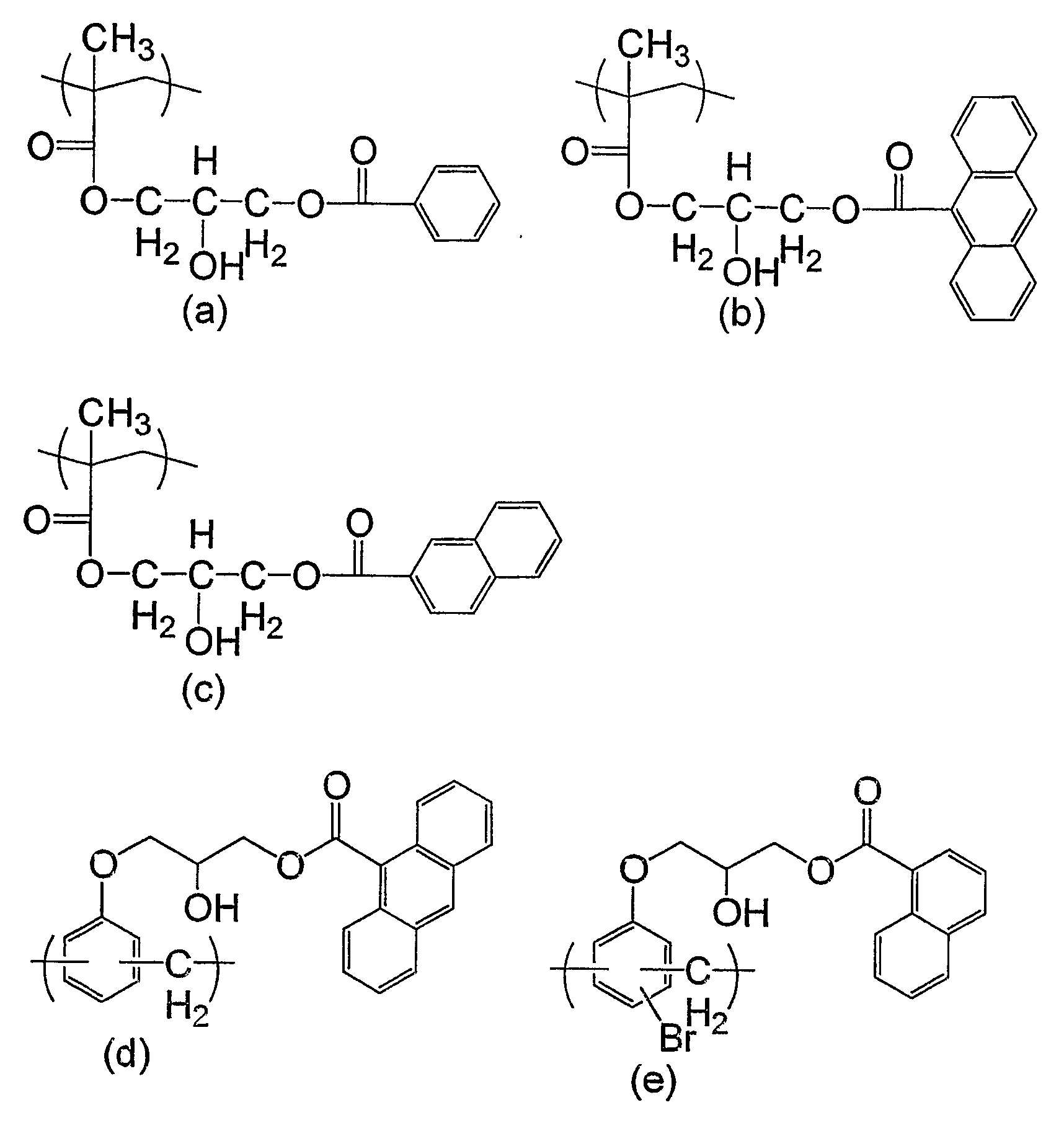
이러한 폴리머로서는, 예를 들면, 벤질 아크릴레이트, 벤질 메타크릴레이트, 페닐 아크릴레이트, 나프틸 아크릴레이트, 안트릴 메타크릴레이트, 안트릴 메틸메타크릴레이트, 스티렌, 히드록시스티렌, 벤질 비닐에테르, N-페닐 말레이미드 등의 부가 중합성 모노머를 그 구조단위로 함유하는 부가 중합계 폴리머나, 페놀노보락, 나프톨노보락 등의 축중합계 폴리머를 들 수 있다. 또한, 미국특허 제6323310호 명세서에 기재되어 있는, 트리아진 화합물(상품명 Cyme 1303, Cyme 11123)로부터 제조되는 폴리머를 들 수 있다. 또한, 하기 (a)~(e)의 구조단위를 가지는 폴러미도 들 수 있다.As such a polymer, for example, benzyl acrylate, benzyl methacrylate, phenyl acrylate, naphthyl acrylate, anthryl methacrylate, anthryl methyl methacrylate, styrene, hydroxy styrene, benzyl vinyl ether, N Addition polymerization type polymers containing addition polymerizable monomers, such as -phenyl maleimide, as the structural unit, and polycondensation type polymers, such as a phenol novolak and a naphthol novolak, are mentioned. Furthermore, the polymer manufactured from the triazine compound (brand name Cyme 1303, Cyme 11123) described in US Pat. No. 6,332,10 can be mentioned. Moreover, the pollen which has a structural unit of the following (a)-(e) is also mentioned.
본 발명의 하층막 형성 조성물로 형성되는 다공질 하층막에 반사 방지 기능이 요구되지 않는 경우에는, 흡광부위로서 기능하는 방향 고리 구조를 가지지 않는 폴리머를 사용할 수 있다. 이러한 폴리머로서는 예를 들면 아크릴 산, 메타크릴 산, 알킬 아크릴레이트, 알킬 메타크릴레이트, 비닐 알콜, 알킬 비닐 에테르, 아크릴로니트릴, 말레이미드, N-알킬 말레이미드, 말레인산 무수물 등의 방향 고리 구조를 가지지 않는 부가 중합성 모노머만 그 구조단위로서 포함하는 부가 중합계 폴리머를 들 수 있다.When the antireflection function is not required for the porous underlayer film formed from the underlayer film-forming composition of the present invention, a polymer having no aromatic ring structure functioning as the light absorption site can be used. Examples of such a polymer include aromatic ring structures such as acrylic acid, methacrylic acid, alkyl acrylate, alkyl methacrylate, vinyl alcohol, alkyl vinyl ether, acrylonitrile, maleimide, N-alkyl maleimide, maleic anhydride, and the like. The addition polymerization type polymer which contains only the addition polymerizable monomer which does not have as a structural unit is mentioned.
본 발명에서, 상기 유기재료로서 부가중합계 폴리머가 사용되는 경우, 그 폴리머는 단독 중합체로도 좋고 공중합체로도 좋다. 부가중합계 폴리머의 제조에는 부가 중합성 모노머가 사용된다. 이러한 부가 중합성 모노머로서는 아크릴산, 메타크릴산, 아크릴산 에스테르 화합물, 메타크릴산 에스테르 화합물, 아크릴아미드 화합물, 메타크릴아미드 화합물, 비닐 화합물, 스티렌 화합물, 말레이미드 화합물, 말레인산 무수물, 아크릴로니트릴 등을 들 수 있다.In the present invention, when an addition polymer-based polymer is used as the organic material, the polymer may be either a homopolymer or a copolymer. An addition polymerizable monomer is used for manufacture of an addition polymerization type polymer. Examples of such an addition polymerizable monomer include acrylic acid, methacrylic acid, acrylic acid ester compound, methacrylic acid ester compound, acrylamide compound, methacrylamide compound, vinyl compound, styrene compound, maleimide compound, maleic anhydride, acrylonitrile, and the like. Can be.
아크릴산 에스테르 화합물로는, 메틸 아크릴레이트, 에틸 아크릴레이트, 노말 헥실 아크릴레이트, 이소 프로필 아크릴레이트, 시클로 헥실 아크릴레이트, 벤질 아크릴레이트, 페닐 아크릴레이트, 안트릴 메틸아크릴레이트, 2-히드록시 에틸 아크릴레이트, 3-클로로-2-히드록시 프로필 아크릴레이트, 2-히드록시 프로필 아크릴레이트, 2,2,2-트리 플루오로 에틸 아크릴레이트, 2,2,2-트리클로로에틸 아크릴레이트, 2-브로모 에틸 아크릴레이트, 4-히드록시 부틸 아크릴레이트, 2-메톡시 에틸 아크릴레이트, 테트라 히드로 푸르푸릴 아크릴레이트, 2-메틸-2-아다만틸 아크릴레이트, 5-아크릴로일옥시-6-히드록시노보넨-2-카르복실릭-6-락톤, 3-아크릴록시 프로필 트리에톡시 실란, 글리시딜 아크릴레이트 등을 들 수 있다.As the acrylic ester compound, methyl acrylate, ethyl acrylate, normal hexyl acrylate, isopropyl acrylate, cyclohexyl acrylate, benzyl acrylate, phenyl acrylate, anthryl methyl acrylate, 2-hydroxy ethyl acrylate , 3-chloro-2-hydroxy propyl acrylate, 2-hydroxy propyl acrylate, 2,2,2-trifluoroethyl acrylate, 2,2,2-trichloroethyl acrylate, 2-bromo Ethyl acrylate, 4-hydroxy butyl acrylate, 2-methoxy ethyl acrylate, tetra hydrofurfuryl acrylate, 2-methyl-2-adamantyl acrylate, 5-acryloyloxy-6-hydroxy Norbornene-2-carboxylic-6-lactone, 3-acryloxy propyl triethoxy silane, glycidyl acrylate and the like.
메타크릴산 에스테르 화합물로는, 메틸 메타크릴레이트, 에틸 메타크릴레이트, 노말 헥실 메타크릴레이트, 이소 프로필 메타크릴레이트, 시클로헥실 메타크릴레이트, 벤질 메타크릴레이트, 페닐 메타크릴레이트, 안트릴 메틸메타크릴레이트, 2-히드록시 에틸 메타크릴레이트, 2-히드록시 프로필 메타크릴레이트, 2,2,2-트리플루오로 에틸 메타크릴레이트, 2,2,2-트리클로로 에틸 메타크릴레이트, 2-브로모 에틸 메타크릴레이트, 4-히드록시 부틸 메타크릴레이트, 2-메톡시 에틸 메타크릴레이트, 테트라 히드로 푸르푸릴 메타크릴레이트, 2-메틸-2-아다만틸 메타크릴레이트, 5-메타크릴로일옥시-6-히드록시노보넨-2-카르복실릭-6-락톤, 3-메타크릴옥시프로필트리에톡시실란 글리시딜 메타크릴레이트, 2-페닐에틸 메타크릴레이트, 히드록시 페닐 메타크릴레이트, 브로모 페닐 메타크릴레이트 등을 들 수 있다.As methacrylic acid ester compound, methyl methacrylate, ethyl methacrylate, normal hexyl methacrylate, isopropyl methacrylate, cyclohexyl methacrylate, benzyl methacrylate, phenyl methacrylate, anthryl methyl meth Acrylate, 2-hydroxy ethyl methacrylate, 2-hydroxy propyl methacrylate, 2,2,2-trifluoro ethyl methacrylate, 2,2,2-trichloro ethyl methacrylate, 2- Bromo ethyl methacrylate, 4-hydroxy butyl methacrylate, 2-methoxy ethyl methacrylate, tetra hydrofurfuryl methacrylate, 2-methyl-2-adamantyl methacrylate, 5-methacryl Royloxy-6-hydroxynorbornene-2-carboxylic-6-lactone, 3-methacryloxypropyltriethoxysilane glycidyl methacrylate, 2-phenylethyl methacrylate, hydroxy phenyl meta Acrylate, Bromo phenyl methacrylate etc. are mentioned.
아크릴아미드 화합물로는, 아크릴아미드, N-메틸아크릴아미드, N-에틸아크릴아미드, N-벤질 아크릴아미드, N-페닐 아크릴아미드, N,N-디메틸 아크릴아미드, N-안트릴 아크릴아미드 등을 들 수 있다.As acrylamide compound, acrylamide, N-methyl acrylamide, N-ethyl acrylamide, N-benzyl acrylamide, N-phenyl acrylamide, N, N- dimethyl acrylamide, N- anthryl acrylamide, etc. are mentioned. Can be.
메타크릴아미드 화합물로는, 메타크릴아미드, N-메틸 메타크릴아미드, N-에틸 메타크릴아미드, N-벤질 메타크릴아미드, N-페닐 메타크릴아미드, N,N-디메틸 메타크릴아미드, N-안트릴 메타크릴아미드 등을 들 수 있다.As a methacrylamide compound, methacrylamide, N-methyl methacrylamide, N-ethyl methacrylamide, N-benzyl methacrylamide, N-phenyl methacrylamide, N, N-dimethyl methacrylamide, N- Anthryl methacrylamide etc. are mentioned.
비닐 화합물로는, 비닐 알콜, 2-히드록시 에틸 비닐 에테르, 메틸 비닐 에테르, 에틸 비닐 에테르, 벤질 비닐 에테르, 비닐 초산(酢酸), 비닐 트리메톡시 실란, 2-클로로 에틸 비닐 에테르, 2-메톡시 에틸 비닐 에테르, 비닐 나프탈렌, 비닐 안트라센 등을 들 수 있다.Examples of the vinyl compound include vinyl alcohol, 2-hydroxy ethyl vinyl ether, methyl vinyl ether, ethyl vinyl ether, benzyl vinyl ether, vinyl acetate, vinyl trimethoxy silane, 2-chloroethyl vinyl ether, and 2-methion. Methoxy ethyl vinyl ether, vinyl naphthalene, vinyl anthracene and the like.
스티렌 화합물로는, 스티렌, 히드록시 스티렌, 클로로 스티렌, 브로모 스티렌, 메톡시 스티렌, 시아노 스티렌, 아세틸 스티렌 등을 들 수 있다.As a styrene compound, styrene, hydroxy styrene, chloro styrene, bromo styrene, methoxy styrene, cyano styrene, acetyl styrene, etc. are mentioned.
말레이미드 화합물로는, 말레이미드, N-메틸 말레이미드, N-페닐 말레이미드, N-시클로헥실 말레이미드, N-벤질 말레이미드, N-히드록시 에틸 말레이미드 등을 들 수 있다.As a maleimide compound, maleimide, N-methyl maleimide, N-phenyl maleimide, N-cyclohexyl maleimide, N-benzyl maleimide, N-hydroxy ethyl maleimide, etc. are mentioned.
본 발명에서, 상기 유기재료로 사용되는 축중합계 폴리머로는, 예를 들면, 글리콜 화합물과 디카본산 화합물의 축중합 폴리머를 들 수 있다. 글리콜 화합물로는 디에틸렌 글리콜, 헥사 메틸렌 글리콜, 부틸렌 글리콜 등을 들 수 있다. 디카본산 화합물로는, 호박산, 아디프산, 테레프탈산, 무수 말레인산 등을 들 수 있다. 또한, 예를 들면, 폴리피로메리트 이미드, 폴리(p-페닐렌테레프탈 아미드), 폴리부틸렌 테레프탈레이트, 폴리에틸렌 테레프탈레이트 등의 폴리에스테르, 폴리아미드, 폴리이미드를 들 수 있다.In the present invention, examples of the polycondensation polymer used as the organic material include a polycondensation polymer of a glycol compound and a dicarboxylic acid compound. Diethylene glycol, hexa methylene glycol, butylene glycol, etc. are mentioned as a glycol compound. Succinic acid, adipic acid, terephthalic acid, maleic anhydride, etc. are mentioned as a dicarboxylic acid compound. Further examples thereof include polyesters such as polypyromerite imide, poly (p-phenylene terephthalamide), polybutylene terephthalate, polyethylene terephthalate, polyamide, and polyimide.
본 발명의 하층막 형성 조성물의 유기재료로 사용되는 폴리머의 분자량으로는, 중량평균 분자량으로, 예를 들면, 1000~1000000이고, 또는 3000~300000이며, 또한, 예를 들면 5000~200000이고, 또는 8000~100000이다.As a molecular weight of the polymer used as the organic material of the underlayer film forming composition of this invention, it is 1000-1 million, or 3000-30000, and is 5000-20000, for example by weight average molecular weight, or 8000 to 100000.
본 발명의 하층막 형성 조성물의 유기재료로 사용되는 가교성 화합물로는, 특별히 그 종류가 한정되지는 않는다.As a crosslinking | crosslinked compound used as the organic material of the underlayer film forming composition of this invention, the kind in particular is not limited.
가교성 화합물로는, 멜라민 화합물, 치환 요소 화합물, 에폭시기를 함유하는 폴리머계 가교성 화합물 등을 들 수 있다. 바람직하게는, 적어도 2개의 가교형성 치환기를 가지는 가교성 화합물이며, 메톡시 메틸화 글리콜 우릴, 또는 메톡시 메틸화 멜라민 등의 화합물이다. 예를 들면, 테트라 메톡시 메틸 글리콜 우릴, 헥사 메톡시 메틸 멜라민, 테트라 메톡시 벤조 구아나민 등이다. 또한, 테트라 메톡시 메틸 요소, 테트라 부톡시 메틸 요소 등의 화합물도 들 수 있다.As a crosslinkable compound, a melamine compound, a substituted element compound, the polymer type crosslinking compound containing an epoxy group, etc. are mentioned. Preferably, it is a crosslinkable compound which has at least 2 crosslinkable substituents, and is a compound, such as methoxy methylated glycol uril or methoxy methylated melamine. For example, tetramethoxy methyl glycol uril, hexa methoxy methyl melamine, tetramethoxy benzoguanamine and the like. Moreover, compounds, such as tetramethoxy methyl urea and tetra butoxy methyl urea, are also mentioned.
이들 가교성 화합물은 자기 축합에 의한 가교반응을 일으킬 수 있다. 또한, 폴리머나 흡광성 화합물과 조합시켜 사용되는 경우, 폴리머나 흡광성 화합물 중에 수산기나 카르복실기 등의 가교성 치환기가 존재하는 경우는, 이들 가교성 치환기 와 가교반응을 일으킬 수 있다.These crosslinkable compounds can cause crosslinking reaction by self-condensation. Moreover, when used in combination with a polymer or a light absorbing compound, when crosslinkable substituents, such as a hydroxyl group and a carboxyl group, exist in a polymer or a light absorbing compound, a crosslinking reaction may be caused with these crosslinkable substituents.
본 발명의 하층막 형성 조성물이 가교성 화합물을 포함하고 있는 경우, 가교반응으로 인하여, 그 조성물로 형성되는 다공질 하층막은 강고한 막으로 된다. 즉, 반도체 기판상에 도포되는 하층막 형성 조성물의 가열에 의한 하층막 형성중에 가교반응이 일어난다. 그 결과, 형성되는 다공질 하층막은 포토레지스트에 사용되는 유기용제, 예를 들면, 에틸렌 글리콜 모노메틸 에테르, 에틸 세로솔브 아세테이트, 디에틸렌 글리콜 모노에틸 에테르, 프로필렌 글리콜, 프로필렌 글리콜 모노메틸 에테르, 프로필렌 글리콜 모노메틸 에테르 아세테이트, 프로필렌 글리콜 프로필 에테르 아세테이트, 톨루엔, 시클로헥사논, 2-히드록시 프로피온산 에틸, 에톡시 초산(酢酸) 에틸, 젖산 에틸, 젖산 부틸 등에 대한 용해성이 낮은 것으로 된다.When the underlayer film-forming composition of the present invention contains a crosslinkable compound, the porous underlayer film formed of the composition becomes a firm film due to the crosslinking reaction. That is, crosslinking reaction occurs during the underlayer film formation by heating of the underlayer film forming composition apply | coated on a semiconductor substrate. As a result, the formed porous underlayer film is an organic solvent used for photoresist, for example, ethylene glycol monomethyl ether, ethyl longitudinal solve acetate, diethylene glycol monoethyl ether, propylene glycol, propylene glycol monomethyl ether, propylene glycol mono The solubility in methyl ether acetate, propylene glycol propyl ether acetate, toluene, cyclohexanone, ethyl 2-hydroxy propionate, ethyl ethoxy acetate, ethyl lactate, butyl lactate, and the like is low.
본 발명의 하층막 형성 조성물의 유기재료로 사용되는 흡광성 화합물은, 특별히 그 종류가 한정되는 것은 아니다.The kind in particular for the light absorbing compound used as the organic material of the underlayer film forming composition of this invention is not limited.
흡광성 화합물의 종류, 첨가량을 선택함으로써, 본 발명의 하층막 형성 조성물로 형성되는 다공질 하층막의 굴절율, 감쇠(減衰)계수 등의 특성을 조절하는 것이 가능하다. 이러한 흡광성 화합물로는, 다공질 하층막의 위에 놓여진 포토 레지스트 층 중의 감광성분의 감광 특성 파장 영역에서의 빛에 대하여 높은 흡수능을 가지는 화합물이 바람직하게 이용된다. 흡광성 화합물은 1종만을 이용할 수도 있지만, 2종이상을 조합시켜 이용할 수도 있다.By selecting the kind and addition amount of a light absorbing compound, it is possible to adjust characteristics, such as refractive index and attenuation coefficient, of the porous underlayer film formed from the underlayer film forming composition of this invention. As such a light absorbing compound, the compound which has a high absorption ability with respect to the light in the photosensitive characteristic wavelength range of the photosensitive component in the photoresist layer put on the porous underlayer film is used preferably. Although only 1 type may be used for a light absorbing compound, it can also be used in combination of 2 or more type.
흡광성 화합물로는, 예를 들면, 페닐 화합물, 벤조페논 화합물, 벤조트리아졸 화합물, 아조 화합물, 나프탈렌 화합물, 안트라센 화합물, 안트라키논 화합물, 트리아진 화합물, 트리아진 트리온 화합물, 키노린 화합물 등을 사용할 수 있다. 페닐 화합물, 나프탈렌 화합물, 안트라센 화합물, 트리아진 화합물, 트리아진 트리온 화합물 등을 이용할 수 있다.As a light absorbing compound, a phenyl compound, a benzophenone compound, a benzotriazole compound, an azo compound, a naphthalene compound, an anthracene compound, an anthraquinone compound, a triazine compound, a triazine trione compound, a quinoline compound etc. are mentioned, for example. Can be used. A phenyl compound, a naphthalene compound, an anthracene compound, a triazine compound, a triazine trione compound, etc. can be used.
흡광성 화합물로는, 적어도 하나의 수산기, 아미노기 또는 카르복실기를 가지는 페닐 화합물, 적어도 하나의 수산기, 아미노기 또는 카르복실기를 가지는 나프탈렌 화합물, 적어도 하나의 수산기, 아미노기 또는 카르복실기를 가지는 안트라센 화합물이 바람직하게 사용된다.As the light absorbing compound, a phenyl compound having at least one hydroxyl group, an amino group or a carboxyl group, a naphthalene compound having at least one hydroxyl group, an amino group or a carboxyl group, an anthracene compound having at least one hydroxyl group, an amino group or a carboxyl group is preferably used.
적어도 하나의 수산기, 아미노기 또는 카르복실기를 가지는 페닐 화합물로는, 페놀, 브로모 페놀, 4,4'-술포닐 디페놀, tert-부틸 페놀, 비페놀, 안식향산, 살리틸산, 히드록시 이소프탈산, 페닐 초산(酢酸), 아닐린, 벤질 아민, 벤질 알콜, 신나밀 알콜, 페닐 아라닌, 페녹시 브로판올, 4-브로모 안식향산, 3-요드 안식향산, 2,4,6-트리브로모 페놀, 2,4,6-트리브로모 레졸시놀, 3,4,5-트리요드 안식향산, 2,4,6-트리요드-3-아미노 안식향산, 2,4,6-트리요드-3-히드록시 안식향산, 2,4,6-트리브로모-3-히드록시 안식향산 등을 들 수 있다.Examples of the phenyl compound having at least one hydroxyl group, amino group or carboxyl group include phenol, bromo phenol, 4,4'-sulfonyl diphenol, tert-butyl phenol, biphenol, benzoic acid, salicylic acid, hydroxy isophthalic acid and phenyl Acetic acid, aniline, benzyl amine, benzyl alcohol, cinnamil alcohol, phenyl alanine, phenoxy bropanol, 4-bromo benzoic acid, 3-iodine benzoic acid, 2,4,6-tribromo phenol, 2, 4,6-tribromo resorcinol, 3,4,5-triiodine benzoic acid, 2,4,6-triiod-3-amino benzoic acid, 2,4,6-triiod-3-hydroxy benzoic acid, 2,4,6-tribromo-3-hydroxy benzoic acid etc. are mentioned.
적어도 하나의 수산기, 아미노기, 또는 카르복실기를 가지는 나프탈렌 화합물로는, 1-나프탈렌 카본산, 2-나프탈렌 카본산, 1-나프톨, 2-나프톨, 1-아미노 나프탈렌, 나프틸 초산(酢酸), 1-히드록시-2-나프탈렌 카본산, 3-히드록시-2-나프탈렌 카본산, 3,7-디히드록시-2-나프탈렌 카본산, 6-브로모-2-히드록시 나프탈렌, 2,6-나프탈렌 디카본산, 등을 들 수 있다. As a naphthalene compound which has at least 1 hydroxyl group, an amino group, or a carboxyl group, 1-naphthalene carboxylic acid, 2-naphthalene carboxylic acid, 1-naphthol, 2-naphthol, 1-amino naphthalene, naphthyl acetate, 1- Hydroxy-2-naphthalene carboxylic acid, 3-hydroxy-2-naphthalene carboxylic acid, 3,7-dihydroxy-2-naphthalene carboxylic acid, 6-bromo-2-hydroxy naphthalene, 2,6-naphthalene Dicarboxylic acid, etc. are mentioned.
적어도 하나의 수산기, 아미노기, 또는 카르복실기를 가지는 안트라센 화합 물로는, 9-안트라센 카본산, 9-히드록시 메틸 안트라센, 1-아미노 안트라센, 등을 들 수 있다.As an anthracene compound which has at least 1 hydroxyl group, an amino group, or a carboxyl group, 9-anthracene carboxylic acid, 9-hydroxy methyl anthracene, 1-amino anthracene, etc. are mentioned.
또한, 흡광성 화합물로는 트리아진 트리온 화합물도 바람직하게 이용된다. 트리아진 트리온 화합물로는, 식 (1) :Moreover, a triazine trione compound is also used suitably as a light absorbing compound. As a triazine trione compound, Formula (1):

의 화합물을 들 수 있다. 여기서, 식 중, X는 (f)~(l)의 기를 나타낸다. The compound of the is mentioned. Here, in formula, X represents the group of (f)-(l).
본 발명의 하층막 형성 조성물에서는, 각종의 용제를 사용할 수 있다. 그러한 용제로서는, 에틸렌 글리콜 모노 메틸 에테르, 에틸렌 글리콜 모노 에틸 에테르, 메틸 세로솔브 아세테이트, 에틸 세로솔브 아세테이트, 디에틸렌 글리콜 모노 메틸 에테르, 디에틸렌 글리콜 모노 에틸 에테르, 프로필렌 글리콜, 프로필렌 글리 콜 모노 메틸 에테르, 프로필렌 글리콜 모노 메틸 에테르 아세테이트, 프로필렌 글리콜 프로필 에테르 아세테이트, 톨루엔, 크실렌, 메틸 에틸 케톤, 시클로 펜타논, 시클로 헥사논, 2-히드록시 프로피온산 에틸, 2-히드록시-2-메틸 프로피온산 에틸, 에톡시 초산(酢酸) 에틸, 히드록시 초산(酢酸) 에틸, 2-히드록시-3-메틸 부탄산 메틸, 3-메톡시 프로피온산 메틸, 3-메톡시 프로피온산 에틸, 3-에톡시 프로피온산 에틸, 3-에톡시 프로피온산 메틸, 피르빈산 메틸, 피르빈산 에틸, 초산(酢酸) 에틸, 초산(酢酸) 부틸, 젖산 에틸, 젖산 부틸, 디메틸 포름 아미드, 디메틸 아세트 아미드, 디메틸 술폭시드, N-메틸피로리돈 등을 이용할 수 있다. 이들 용제는 단독으로, 또는 2종이상을 조합하여 사용된다.In the underlayer film forming composition of the present invention, various solvents can be used. As such a solvent, ethylene glycol mono methyl ether, ethylene glycol mono ethyl ether, methyl serosolve acetate, ethyl serosolve acetate, diethylene glycol mono methyl ether, diethylene glycol mono ethyl ether, propylene glycol, propylene glycol mono methyl ether, Propylene Glycol Monomethyl Ether Acetate, Propylene Glycol Propyl Ether Acetate, Toluene, Xylene, Methyl Ethyl Ketone, Cyclopentanone, Cyclohexanone, Ethyl 2-hydroxy Propionate, Ethyl 2-hydroxy-2-methyl Propionate, Ethoxy Acetic Acid (Iii) ethyl, hydroxy ethyl acetate, methyl 2-hydroxy-3-methyl butanoate, methyl 3-methoxy propionate, ethyl 3-methoxy propionate, ethyl 3-ethoxy propionate, 3-ethoxy Methyl Propionate, Methyl Pyrate, Ethyl Pyrate, Ethyl Acetate, Butyl Acetate, Ethyl lactate, butyl lactate, dimethyl formamide, dimethyl acetamide, dimethyl sulfoxide, N-methylpyrrolidone and the like can be used. These solvents are used individually or in combination of 2 or more types.
본 발명에서 하층막 형성조성물의 다른 하나는, 발포성기를 가지는 폴리머 및 용제로 이루어진 것, 또는, 발포성 기를 가지는 폴리머, 유기재료 및 용재로 이루어진 것이다. 또한, 임의성분으로서 가교촉매, 계면활성제 등을 포함하는 것이다. 하층막 형성조성물에서 고형분은, 예를 들면 0.1~50 질량%이고, 또한, 예를 들면 5~40 질량%이며, 또는, 10~35 질량%이다. 여기서 고형분은, 하층막 형성 조성물의 전성분으로부터 용제성분을 제외한 것이다.Another one of the underlayer film-forming compositions in the present invention is composed of a polymer having a foamable group and a solvent, or a polymer having a foamable group, an organic material and a solvent. Moreover, a crosslinking catalyst, surfactant, etc. are contained as an optional component. Solid content in an underlayer film formation composition is 0.1-50 mass%, for example, 5-40 mass%, or 10-35 mass%. Solid content remove | excludes a solvent component from all the components of an underlayer film forming composition here.
여기서, 발포성기를 가지는 폴리머는 필수성분이고, 하층막을 형성하는 성분인 동시에, 하층막을 다공질로 하는 것이다. 유기재료는, 하층막을 형성하는 성분이다. 또한, 본 발명의 하층막 형성 조성물은, 스핀코팅법 등에 의해 반도체 기판상에 도포하는 태양으로 사용되기 때문에, 용액이다.Herein, the polymer having an expandable group is an essential component, a component for forming the underlayer film, and the underlayer film is made porous. An organic material is a component which forms an underlayer film. Moreover, since the underlayer film forming composition of this invention is used by the aspect apply | coated on a semiconductor substrate by a spin coating method etc., it is a solution.
본 발명의 하층막 형성 조성물이 발포성기를 가지는 폴리머, 유기재료 및 용제로 이루어진 경우, 그 고형분에서의 발포성기를 가지는 폴리머의 비율은, 예를 들면 50~95 질량%이고, 또한, 예를 들면 60~90 질량% 이며, 또한, 65~85 질량%이다. 그리고, 고형분에서의 유기재료의 비율은, 예를 들면, 5~50 질량%이고, 또한, 예를 들면 10~40 질량%이고, 또한, 15~35 질량% 이다. 발포성기를 가지는 폴리머의 비율이 이것보다도 작은 경우는, 형성되는 하층막의 다공질성이 충분하지 않게 된다. 그리고, 유기재료 및 용제로서는 상기와 동일한 것을 사용할 수 있다.When the underlayer film forming composition of this invention consists of a polymer which has a foamable group, an organic material, and a solvent, the ratio of the polymer which has a foamable group in the solid content is 50-95 mass%, for example, 60- It is 90 mass% and is 65-85 mass%. And the ratio of the organic material in solid content is 5-50 mass%, for example, 10-40 mass%, and is 15-35 mass%. When the ratio of the polymer which has a foamable group is smaller than this, the porous property of the underlayer film formed will become insufficient. And the same thing as the above can be used as an organic material and a solvent.
본 발명의 하층막 형성 조성물에는, 산 화합물 또는 산 발생제를 첨가할 수 있다. 산 화합물 또는 산발생제는, 상기 가교반응의 촉매로서의 역할을 가지는 것이다.An acid compound or an acid generator can be added to the underlayer film forming composition of this invention. An acid compound or an acid generator has a role as a catalyst of the said crosslinking reaction.
그러한 산 화합물 또는 산 발생제로서는, p-톨루엔 술폰산, 트리 플루오로 메탄 술폰산, 피리디늄-p-톨루엔 술폰산, 살리틸산, 술포 살리틸산, 구연산, 안식향산, 히드록시 안식향산 등의 산 화합물, 또는, 2,4,4,6-테트라 브로모 시클로 헥사 디에논, 2-니트로 벤질 토실레이트, 비스(4-t-부틸페닐)요드늄 트리플루오로 메탄 술포네이트, 트리 페닐 술포늄 트리 플루오로 메탄 술포네이트, 페닐 비스(트리클로로메틸)-s-트리아진, 벤조인 토실레이트, N-히드록시 숙신 이미드 트리플루오로 메탄 술포네이트 등의 산 발생제를 들 수 있다.Examples of such acid compounds or acid generators include acid compounds such as p-toluene sulfonic acid, trifluoromethane sulfonic acid, pyridinium-p-toluene sulfonic acid, salicylic acid, sulfosaltylic acid, citric acid, benzoic acid, and hydroxy benzoic acid, or 2 , 4,4,6-tetrabromocyclohexahexaenone, 2-nitrobenzyl tosylate, bis (4-t-butylphenyl) iodium trifluoro methane sulfonate, triphenyl sulfonium trifluoro methane sulfonate And acid generators such as phenyl bis (trichloromethyl) -s-triazine, benzoin tosylate and N-hydroxy succinimide trifluoro methane sulfonate.
이들 산 화합물 또는 산 발생제 화합물의 첨가량은, 고형분 중에서 10 질량% 이하이고, 예를 들면, 0.02~10 질량%이며, 또한, 예를 들면 0.04~5 질량%이다.The addition amount of these acid compounds or acid generator compounds is 10 mass% or less in solid content, for example, 0.02-10 mass%, and is 0.04-5 mass%, for example.
또한, 본 발명의 하층막 형성 조성물에는, 상기 이외에 필요에 따라 레올로지 조정제, 접착보조제, 계면활성제 등을 첨가할 수 있다.Moreover, a rheology modifier, an adhesion | attachment adjuvant, surfactant, etc. can be added to the underlayer film forming composition of this invention as needed other than the above.
레올로지 조정제는, 주로 하층막 형성 조성물의 유동성을 향상시키고, 특히 가열공정에서, 홀 내부로의 하층막 형성 조성물의 충진성을 높일 목적으로 첨가된다. 구체예로서는, 예를 들면, 디메틸 프탈레이트, 디에틸 프탈레이트, 디이소부틸 프탈레이트, 부틸 이소데실 프탈레이트 등의 프탈산 유도체, 디노말부틸 아디페이트, 디이소옥틸 아디페이트, 옥틸데실 아디페이트 등의 아디핀산 유도체, 디노말 부틸 말레이트, 디에틸 말레이트, 디노닐 말레이트 등의 말레인산 유도체, 메틸 올레이트, 부틸 올레이트, 테트라 히드로 푸르푸릴 올레이트 등의 올레인산 유도체, 및 노말부틸 스테아레이트, 글리세릴 스테아레이트 등의 스테아린산 유도체를 들 수 있다. 이들 레올로지 조정제는, 하층막 형성 조성물의 고형분 중에서, 20 질량% 미만의 비율로 첨가된다.The rheology modifier is mainly added for the purpose of improving the fluidity of the underlayer film-forming composition, and particularly in the heating step, to increase the filling property of the underlayer film-forming composition into the hole. As a specific example, For example, phthalic acid derivatives, such as dimethyl phthalate, diethyl phthalate, diisobutyl phthalate, butyl isodecyl phthalate, dinormalyl adipate, diisooctyl adipate, and adipic acid derivatives, such as octyldecyl adipate, Maleic acid derivatives such as di-normal butyl maleate, diethyl maleate, and dinonyl maleate, oleic acid derivatives such as methyl oleate, butyl oleate and tetrahydrofurfuryl oleate, and normal butyl stearate and glyceryl stearate And stearic acid derivatives thereof. These rheology modifiers are added in the ratio of less than 20 mass% in solid content of an underlayer film forming composition.
접착 보조제는, 주로 반도체 기판 혹은 반사 방지막 또는 포토 레지스트층과 하층막의 밀착성을 향상시키고, 특히 현상(現像)에서 박리하지 않도록 하는 목적으로 첨가된다. 구체예로서는, 예를 들면, 트리메틸 클로로 실란, 디메틸 비닐 클로로 실란, 클로로 메틸 디메틸 클로로 실란 등의 클로로 실란류, 트리메틸 메톡시 실란, 디메틸 디에톡시 실란, 디메틸 비닐 에톡시 실란, γ-메타크릴옥시 프로필 트리메톡시 실란, 디페닐 디메톡시 실란 등의 알콕시 실란류, 헥사메틸 디실라잔, N,N'-비스(트리메틸시릴)우레아, 디메틸 트리메틸 시릴 아민, 트리메틸 시릴 이미다졸 등의 실라잔류, γ-클로로 프로필 트리메톡시 실란, γ-아미노 프로필 트리에톡시 실란, γ-글리시독시 프로필 트리메톡시 실란, γ-메타크릴옥시 프로필 트리메톡시 실란 등의 실란류, 벤조 트리아졸, 벤즈 이미다졸, 인다졸, 이미다졸, 2-메캅토 벤즈 이미다졸, 2-메캅토 벤조 옥사졸, 우라졸, 티오우라실, 메캅토 피리미딘 등의 복소고리식 화합물(複素環式 化合物), 1,1-디메틸 우레아, 1,3-디메틸우레아 등의 요소화합물,을 들 수 있다. 이들 접착 보조제는, 하층막 형성 조성물의 고형분 중에서, 통상 10 질량% 미만, 바람직하게는 5 질량% 미만의 비율로 첨가된다.An adhesion aid is mainly added in order to improve the adhesiveness of a semiconductor substrate, an antireflection film, or a photoresist layer, and an underlayer film, and to prevent it from peeling especially in image development. As specific examples, for example, chlorosilanes such as trimethyl chlorosilane, dimethyl vinyl chlorosilane, chloromethyl dimethyl chloro silane, trimethyl methoxy silane, dimethyl diethoxy silane, dimethyl vinyl ethoxy silane, γ-methacryloxy propyl tree Alkoxy silanes, such as methoxy silane and diphenyl dimethoxy silane, Silazanes, such as hexamethyl disilazane, N, N'-bis (trimethylsilyl) urea, dimethyl trimethylsilyl amine, and trimethyl cyryl imidazole, (gamma) -chloro Silanes such as propyl trimethoxy silane, γ-amino propyl triethoxy silane, γ-glycidoxy propyl trimethoxy silane, γ-methacryloxy propyl trimethoxy silane, benzotriazole, benzimazole, and Heterocyclic compounds such as sol, imidazole, 2-mercapto benz imidazole, 2-mercapto benzoxazole, urasol, thiouracil, and mecapto pyrimidine (複 素 環 式 化合) ) It includes a urea compound such as 1,1-dimethyl urea, 1,3-dimethyl urea. These adhesion aids are normally added in the ratio of less than 10 mass%, Preferably it is less than 5 mass% in solid content of an underlayer film forming composition.
본 발명의 하층막 형성 조성물에는, 핀홀이나 스트레이션등의 발생을 억제하고, 또한, 도포성을 향상시키기 위하여, 계면활성제를 첨가할 수 있다. 계면활성제로서는, 예를 들면 폴리 옥시 에틸렌 라우릴 에테르, 폴리 옥시 에틸렌 스테아릴 에테르, 폴리 옥시 에틸렌 올레일 에테르 등의 폴리 옥시 에틸렌 알킬 에테르류, 폴리옥시 에틸렌 옥틸 페놀 에테르, 폴리 옥시 에틸렌 노닐 페놀 에테르 등의 폴리 옥시 에틸렌 알킬 알릴 에테르류, 폴리 옥시 에틸렌?폴리 옥시 프로필렌 블록 코폴리머류, 솔비탄 모노 라우레이트, 솔비탄 모노 팔미테이트, 솔비탄 모노 스테아레이트, 솔비탄 트리 올레이트, 솔비탄 트리 스테아레이트 등의 솔비탄 지방산 에스테르류, 폴리 옥시 에틸렌 솔비탄 모노 라우레이트, 폴리 옥시 에틸렌 솔비탄 모노 팔미테이트, 폴리 옥시 에틸렌 솔비탄 모노 스테아레이트, 폴리 옥시 에틸렌 솔비탄 트리 스테아레이트 등의 폴리 옥시 에틸렌 솔비탄 지방산 에스테르류 등의 논이온계 계면활성제, 상품명 에프탑 EF301, EF303, EF352((주) 토켐 프로닥츠 제품), 상품명 메가팩 F171, F173, R-08, R-30 (다이닛뽄 잉키 (주) 제품), 후로라도 FC430, FC431 (스미토모 스리엠 (주) 제품), 상품명 아사히가드 AG710, 사프론 S-382, SC101, SC102, SC103, SC104, SC105, SC106(욱초자(旭硝子) (주) 제품) 등의 불소계 계면활성제, 오르가노 실록산 폴리머 KP-341(신에츠 화학공업 (주) 제품) 등을 들 수 있다. 이들 계면활성제의 첨가량은, 하층막 형성조성물의 고형분 중에, 통상 0.5 질량% 이하, 바람직하게는 0.2 질량% 이하이다. 이들 계면활성제는 단독으로 첨가하여도 좋고, 또한 2종이상을 조합시켜 첨가할 수도 있다.Surfactant can be added to the underlayer film forming composition of this invention in order to suppress generation | occurrence | production of a pinhole, a straightening, etc., and to improve applicability | paintability. As surfactant, For example, polyoxyethylene alkyl ethers, such as polyoxyethylene lauryl ether, polyoxyethylene stearyl ether, polyoxyethylene oleyl ether, polyoxyethylene octyl phenol ether, polyoxyethylene nonyl phenol ether, etc. Polyoxyethylene alkyl allyl ethers, polyoxyethylene-polyoxypropylene block copolymers, sorbitan monolaurate, sorbitan mono palmitate, sorbitan monostearate, sorbitan trioleate, sorbitan tristearate Polyoxyethylene sorbitan, such as sorbitan fatty acid esters, polyoxyethylene sorbitan monolaurate, polyoxyethylene sorbitan mono palmitate, polyoxyethylene sorbitan monostearate, polyoxyethylene sorbitan tristearate Nonionic systems, such as fatty acid esters Surfactant, brand name F-top EF301, EF303, EF352 (made by Tochem Prof. Co., Ltd.), brand name Megapack F171, F173, R-08, R-30 (made by Dainippon Inky Co., Ltd.), Furorado FC430, FC431 Fluorine-based surfactants such as (Sumitomo Srim Co., Ltd.), trade names Asahigard AG710, Saffron S-382, SC101, SC102, SC103, SC104, SC105, SC106 (manufactured by Ukcho Co., Ltd.) Kano siloxane polymer KP-341 (made by Shin-Etsu Chemical Co., Ltd.), etc. are mentioned. The addition amount of these surfactant is 0.5 mass% or less normally, Preferably it is 0.2 mass% or less in solid content of an underlayer film formation composition. These surfactants may be added alone, or may be added in combination of two or more types.
이하, 본 발명의 하층막 형성 조성물의 사용에 관하여 설명한다.Hereinafter, use of the underlayer film forming composition of this invention is demonstrated.
반도체에 사용되는 기판(예를 들면, 실리콘/이산화 실리콘 피복기판, 실리콘 나이트라이드 기판, 글래스 기판, ITO 기판, 폴리 이미드 기판, 저유전율 재료(low-k 재료) 피복 기판등)의 위에, 스피너, 코터 등의 적당한 도포 방법에 의해 본 발명의 하층막 형성 조성물이 도포되고, 그 후, 가열함으로써 다공질 하층막이 형성된다. 가열하는 조건으로는, 가열온도 60℃~250℃, 가열시간 0.5~60분사이 중에서 적의, 선택된다. 이것에 의해, 균일한 공공을 가지는 다공질 하층막이 형성된다.Spinners on substrates (e.g., silicon / silicon dioxide coated substrates, silicon nitride substrates, glass substrates, ITO substrates, polyimide substrates, low-k materials coated substrates, etc.) used for semiconductors The underlayer film forming composition of this invention is apply | coated by suitable coating methods, such as a coater, and a porous underlayer film is formed by heating after that. As conditions to heat, it is suitably selected from heating temperature of 60 degreeC-250 degreeC, and heating time of 0.5 to 60 minutes. As a result, a porous underlayer film having uniform pores is formed.
이어서, 그 다공질 하층막 위에, 포토 레지스트 층이 형성되고, 그 후, 미리 설정된 마스크를 통하여 노광시키고, 알칼리성 수용액 등의 현상액에 의해 현상되어, 패턴화된 포토 레지스트가 형성된다. 또한, 필요에 따라 노광후 가열(PEB : Post Exposure Bake)을 행할 수도 있다. 다공질 하층막 위에 형성된 포토 레지스트로서는 특별한 제한은 없고, 범용되고 있는 네가티브형 포토레지스트, 포지티브형 포토레지스트 중 어느것도 사용가능하다.Subsequently, a photoresist layer is formed on the porous underlayer film, and then exposed through a preset mask, and developed with a developing solution such as an alkaline aqueous solution to form a patterned photoresist. In addition, a post exposure bake (PEB) may be performed as necessary. There is no restriction | limiting in particular as a photoresist formed on a porous underlayer film, Any of the general-purpose negative type photoresist and positive type photoresist can be used.
그 후, 포토레지스트가 제거된 부분의 다공질 하층막이 에칭에 의해 제거되고, 반도체 기판을 부분적으로 노출시킨다. 에칭은, 상기 테트라 플루오로 메탄, 퍼 플루오로 시클로 부탄 등을 이용하여 행해진다.Thereafter, the porous underlayer film of the portion where the photoresist has been removed is removed by etching, and partially exposes the semiconductor substrate. Etching is performed using the said tetrafluoromethane, perfluoro cyclobutane, etc.
본 발명에서는, 하층막이 다공질 하층막이기 때문에, 그 에칭에 의한 제거는 다공질이 아닌 하층막에 비하여, 단시간에 완료할 수 있다. 그 결과, 포토 레지스트의 막두께 감소량을 억제할 수 있다. 이것에 의해, 반도체 기판의 가공시에 보호막으로 사용되는 패턴화된 포토 레지스트 및 하층막을 형성할 수 있다.In the present invention, since the underlayer film is a porous underlayer film, removal by etching can be completed in a short time as compared with the underlayer film which is not porous. As a result, the film thickness reduction amount of a photoresist can be suppressed. Thereby, the patterned photoresist and underlayer film used as a protective film at the time of processing a semiconductor substrate can be formed.
드라이 에칭에 의한 제거는, 그 제거되는 층에 포함되는 방향 고리 구조의 비율이 커질수록 그 속도가 작게 된다고 알려져 있다. 그 때문에, 본 발명의 다공질 하층막에서는, 그 드라이 에칭에 의한 제거 속도를 보다 크게 하고 싶은 경우에는, 사용되는 하층막 형성 조성물에 포함되는 방향 고리 구조의 양을 적게 하면 좋다. 특히, 그 조성물 중의 발포성기를 가지는 폴리머 성분 또는 폴리머 성분에 포함되는 방향 고리 구조의 양을 적게 하면 좋다. 따라서, 드라이 에칭에 의한 제거속도가 큰 다공질 하층막이 요구되는 경우에는, 그 구조내에 방향 고리 구조를 가지지 않는 발포성기를 가지는 폴리머 성분 또는 폴리머가 바람직하게 이용된다.It is known that the removal by dry etching becomes small as the ratio of the aromatic ring structure contained in the removed layer becomes large. Therefore, in the porous underlayer film of this invention, when the removal rate by the dry etching is to be made larger, what is necessary is just to reduce the quantity of the aromatic ring structure contained in the underlayer film forming composition used. In particular, the amount of the aromatic ring structure contained in the polymer component or polymer component having an expandable group in the composition may be reduced. Therefore, when a porous underlayer film having a high removal rate by dry etching is desired, a polymer component or a polymer having a foamable group having no aromatic ring structure in the structure is preferably used.
포지티브형 포토 레지스트의 현상액으로는, 수산화 나트륨, 수산화 칼륨, 탄산 나트륨, 규산 나트륨, 메타 규산 나트륨, 암모니아 수 등의 무기 알칼리류, 에틸 아민, n-프로필 아민 등의 제1 아민류, 디에틸 아민, 디-n-부틸 아민 등의 제2 아민류, 트리에틸 아민, 메틸 디에틸 아민 등의 제3 아민류, 디메틸 에탄올 아민, 트리에탄올 아민 등의 알콜 아민류, 테트라 메틸 암모늄 히드록시드, 테트라 에틸 암모늄 히드록시드, 콜린 등의 제4급 암모늄염, 피롤, 피페리딘 등의 환상 아민류, 등의 알칼리 류의 수용액을 사용할 수 있다. 또한, 상기 알칼리류의 수용액에 이소 프로필 알콜 등의 알콜류, 아니온계 등의 계면활성제를 적당량 첨가하여 사용할 수도 있다. 이들 중에서 바람직한 현상액은 제4급 암모늄염, 더욱 바람직하게는 테트라 메틸 암모늄 히드록시드 및 콜린이다.Examples of the developer of the positive photoresist include inorganic alkalis such as sodium hydroxide, potassium hydroxide, sodium carbonate, sodium silicate, sodium metasilicate and aqueous ammonia, first amines such as ethyl amine and n-propyl amine, diethyl amine, Second amines such as di-n-butyl amine, third amines such as triethyl amine and methyl diethyl amine, alcohol amines such as dimethyl ethanol amine and triethanol amine, tetra methyl ammonium hydroxide, tetra ethyl ammonium hydroxide And aqueous solutions of alkalis such as cyclic amines such as quaternary ammonium salts such as choline, pyrrole and piperidine, and the like can be used. Moreover, alcohols, such as isopropyl alcohol, and surfactant, such as an anionic type, can also be added and used for the said aqueous solution of alkalis. Preferred developers among these are quaternary ammonium salts, more preferably tetra methyl ammonium hydroxide and choline.
또한, 본 발명의 다공질 하층막의 상층에는, 포토 레지스트의 도포, 형성전에 반사 방지막층이 도포, 형성되는 경우가 있다. 여기서 사용되는 반사 방지막 조성물로는 특별한 제한은 없고, 지금까지 리소그라피 프로세스에서 관용되고 있는 것 중에서 임으로 선택하여 사용할 수 있으며, 또한, 관용되고 있는 방법, 예를 들면, 스피너, 코터에 의한 도포 및 소성에 의해 반사 방지막의 형성을 행할 수 있다. 반사 방지막 조성물로는, 예를 들면, 흡광성 화합물, 수지 및 용제를 주성분으로 하는 것, 화학결합에 의해 연결한 흡광성기를 가지는 수지, 가교제 및 용제를 주성분으로 하는 것, 흡광성 화합물, 가교제 및 용제를 주성분으로 하는 것, 흡광성을 가지는 고분자 가교제 및 용제를 주성분으로 하는 것, 등을 들 수 있다. 이들 반사 방지막 조성물은 또한, 필요에 따라, 산성분, 산발생제 성분, 레올로지 조정제 등을 포함할 수 있다. 흡광성 화합물로서는, 반사 방지막의 위에 설치한 포토 레지스트 중의 감광성분의 감광특성 파장 영역에서의 빛에 대하여 높은 흡수능을 가지는 것이면 이용할 수 있고, 예를 들면, 벤조 페논 화합물, 벤조 트리아졸 화합물, 아조 화합물, 나프탈렌 화합물, 안트라센 화합물, 안트라키논 화합물, 트리아진 화합물 등을 들 수 있다. 수지로서는, 폴리에스테르, 폴리이미드, 폴리스티렌, 노보락 수지, 폴리아세탈 수지, 아크릴 수지 등을 들 수 있다. 화학결합에 의해 연결한 흡광성기를 가지는 수지로서는, 안트라센 고리, 나프탈렌 고리, 벤젠 고리, 키노린 고리, 키녹사린 고리, 티아졸 고리라는 흡광성 방향 고리 구조를 가지는 수지를 들 수 있다.In addition, an antireflection film layer may be applied and formed on the upper layer of the porous underlayer film of the present invention before the application and formation of the photoresist. There is no restriction | limiting in particular as an anti-reflective film composition used here, It can select arbitrarily and can use from the thing conventionally used by the lithography process, and also it is used for the method and the method currently used, for example, the application and baking by a spinner, a coater. The antireflection film can be formed by this. Examples of the antireflection film composition include a light absorbing compound, a resin and a solvent as main components, a resin having a light absorbing group connected by chemical bonding, a crosslinking agent and a solvent as main components, a light absorbing compound, a crosslinking agent, and The solvent as a main component, the polymer crosslinking agent which has light absorbency, and a solvent as a main component are mentioned. These antireflective film compositions may also contain an acid component, an acid generator component, a rheology modifier, etc. as needed. As a light absorbing compound, it can use if it has high absorption ability with respect to the light in the photosensitive characteristic wavelength range of the photosensitive component in the photoresist provided on the anti-reflective film, For example, a benzophenone compound, a benzotriazole compound, an azo compound And naphthalene compounds, anthracene compounds, anthraquinone compounds, triazine compounds and the like. As resin, polyester, polyimide, polystyrene, a novolak resin, a polyacetal resin, an acrylic resin etc. are mentioned. As resin which has the light absorbing group connected by chemical bond, resin which has the light absorbing aromatic ring structure of an anthracene ring, a naphthalene ring, a benzene ring, a quinoline ring, a quinoxarine ring, and a thiazole ring is mentioned.
본 발명의 하층막 형성 조성물로 형성되는 다공질 하층막은, 또한, 리소그라피 프로세스에 사용되는 빛의 파장에 의해서는, 그 빛을 흡수하는 것이 있고, 그러한 경우에는, 기판부터의 반사광을 방지하는 효과를 가지는 층으로 기능할 수 있다. 또한, 본 발명의 다공질 하층막은, 기판과 포토 레지스트의 상호작용을 방지하기 위한 층, 포토 레지스트에 이용되는 재료 또는 포토 레지스트의 노광시에 생성하는 물질의 기판으로의 나쁜 작용을 방지하는 기능을 가지는 층, 가열시에 기판에서부터 생성하는 물질의 상층 포토 레지스트로의 확산, 나쁜 작용을 방지하는 기능을 가지는 층, 으로 작용하는 것도 가능하다.The porous underlayer film formed from the underlayer film forming composition of the present invention may further absorb the light depending on the wavelength of the light used in the lithography process, and in such a case, has an effect of preventing the reflected light from the substrate. Can function as a layer. In addition, the porous underlayer film of the present invention has a function of preventing a bad effect of a layer for preventing the interaction between the substrate and the photoresist, a material used for the photoresist, or a substance produced upon exposure of the photoresist to the substrate. It is also possible to act as a layer, a layer having a function of preventing diffusion of a substance produced from the substrate into the upper photoresist upon heating and a bad effect.
이하, 본 발명을 실시예에 의해 보다 구체적으로 설명하지만, 이것에 의해 본 발명이 한정되는 것은 아니다.Hereinafter, although an Example demonstrates this invention more concretely, this invention is not limited by this.
실시예Example
합성례1Synthesis Example 1
프로필렌 글리콜 모노 메틸 에테르 27.91g에, 2-히드록시 프로필렌 메타크릴레이트 20.93g과 벤질 메타크릴레이트 6.98g을 용해시키고, 반응액 중에 질소를 30분 흘린 후, 70℃로 승온하였다. 반응용액을 70℃에 유지하면서 아조 비스 이소 부틸로 니트릴 0.3g을 첨가하고, 질소분위기하, 70℃에서 24시간 교반함으로써, 2-히드록시 프로필 메타크릴레이트와 벤질 메타크릴레이트의 공중합 폴리머의 용액을 얻었다. 얻어진 폴리머의 GPC 분석을 행할 때, 중량평균분자량은 15000(표준 폴리스티렌 환산)이었다.20.93 g of 2-hydroxy propylene methacrylate and 6.98 g of benzyl methacrylate were dissolved in 27.91 g of propylene glycol monomethyl ether, and after flowing nitrogen in the reaction solution for 30 minutes, the temperature was raised to 70 ° C. A solution of the copolymer of 2-hydroxypropyl methacrylate and benzyl methacrylate is added by adding 0.3 g of azo bis isobutyl nitrile while maintaining the reaction solution at 70 ° C. and stirring the mixture at 70 ° C. for 24 hours under a nitrogen atmosphere. Got. When GPC analysis of the obtained polymer was performed, the weight average molecular weight was 15000 (standard polystyrene conversion).
합성례2Synthesis Example 2
젖산 에틸 30g에, 2-히드록시 에틸 아크릴레이트 30g을 용해시키고, 반응액 중에 질소를 30분 흘린 후, 70℃로 승온하였다. 반응용액을 70℃에 유지하면서 아조 비스 이소 부틸로 니트릴 0.3g을 첨가하고, 질소분위기하, 70℃에서 24시간 교반함으로써, 폴리(2-히드록시 에틸)아크릴레이트의 용액을 얻었다. 얻어진 폴리머의 GPC분석을 행하였을 때, 중량평균분자량은 9800(표준 폴리스티렌 환산)이었다.30 g of 2-hydroxyethyl acrylate was dissolved in 30 g of ethyl lactate, and after flowing nitrogen in the reaction solution for 30 minutes, the temperature was raised to 70 ° C. While maintaining the reaction solution at 70 ° C, 0.3 g of azo bis isobutylnitrile was added, followed by stirring at 70 ° C for 24 hours under a nitrogen atmosphere to obtain a solution of poly (2-hydroxyethyl) acrylate. When GPC analysis of the obtained polymer was performed, the weight average molecular weight was 9800 (standard polystyrene equivalent).
실시예1Example 1
합성례1에서 얻은 폴리머 5g을 포함하는 용액 10g에, 헥사 메톡시 메틸 멜라민 1.15g, 피리디늄-p-톨루엔 술폰산 0.012g, 프로필렌 글리콜 모노 메틸 에테르 0.77g 및 디메틸 술폭시드 8.66g을 첨가하고, 30.0% 용액으로 한 후, 발포제 4,4-옥시 비스 벤젠 술포닐 히드라지드 0.309g(고형분 중 5%)를 첨가하였다. 그리고, 공공 직경 0.2㎛인 폴리에틸렌제 마이크로필터를 이용하여 여과하여, 하층막 형성 조성물 용액을 제조하였다.To 10 g of the solution containing 5 g of the polymer obtained in Synthesis Example 1, 1.15 g of hexamethoxy methyl melamine, 0.012 g of pyridinium-p-toluene sulfonic acid, 0.77 g of propylene glycol mono methyl ether, and 8.66 g of dimethyl sulfoxide were added, and 30.0 was added. After making up% solution, 0.309 g (5% in solids) of blowing agent 4,4-oxy bis benzene sulfonyl hydrazide was added. And it filtered using the polyethylene microfilter with a pore diameter of 0.2 micrometer, and produced the underlayer film forming composition solution.
실시예2Example 2
합성례1에서 얻은 폴리머 5g을 포함하는 용액 10g에, 헥사 메톡시 메틸 멜라민 1.15g, 피리디늄-p-톨루엔 술폰산 0.012g, 프로필렌 글리콜 모노 메틸 에테르 0.77g, 및 디메틸 술폭시드 8.66g을 첨가하고, 30.0% 용액으로 한 후, 발포제 아조 디카본 아미드 0.124g(전고형분 중 2%)를 첨가하였다. 그리고, 공공 직경 0.2㎛인 폴리에틸렌제 마이크로필터를 이용하여 여과하여, 하층막 형성 조성물의 용액을 제조하였다.To 10 g of a solution containing 5 g of the polymer obtained in Synthesis Example 1, 1.15 g of hexamethoxy methyl melamine, 0.012 g of pyridinium-p-toluene sulfonic acid, 0.77 g of propylene glycol mono methyl ether, and 8.66 g of dimethyl sulfoxide were added. After a 30.0% solution, 0.124 g (2% in total solids) of blowing agent azo dicarbon amide was added. And it filtered using the polyethylene microfilter with a pore diameter of 0.2 micrometer, and prepared the solution of the underlayer film forming composition.
실시예3Example 3
합성례2에서 얻은 폴리머 5g을 포함하는 용액 10g에, 헥사메톡시 메틸 멜라민 1.15g, 피리디늄-p-톨루엔 술폰산 0.012g, 프로필렌 글리콜 모노 메틸 에테르 0.77g, 및 디메틸 술폭시드 8.66g을 첨가하여, 30.0% 용액으로 한 후, 발포제 아조 디카본 아미드 0.124(전고형분 중 2%)를 첨가하였다. 그리고, 공공직경 0.2㎛인 폴리에틸렌제 마이크로필터를 이용하여 여과하여, 하층막 형성 조성물의 용액을 제조하였다.To 10 g of the solution containing 5 g of the polymer obtained in Synthesis Example 2, 1.15 g of hexamethoxy methyl melamine, 0.012 g of pyridinium-p-toluene sulfonic acid, 0.77 g of propylene glycol mono methyl ether, and 8.66 g of dimethyl sulfoxide were added. After making 30.0% solution, 0.124 (2% in total solids) of blowing agent azo dicarbon amide was added. And it filtered using the polyethylene microfilter with a pore diameter of 0.2 micrometer, and prepared the solution of the underlayer film forming composition.
비교예1Comparative Example 1
합성례1에서 얻은 폴리머 5g을 포함하는 용액 10g에, 헥사 메톡시 메틸 멜라민 1.15g, 피리디늄-p-톨루엔 술폰산 0.012g, 프로필렌 글리콜 모노 메틸 에테르 0.77g, 및 디메틸 술폭시드 8.66g을 첨가하여, 30.0% 용액으로 하였다. 그리고, 공공 직경 0.05㎛인 폴리에틸렌제 마이크로필터를 이용하여 여과하여, 발포제를 포함하지 않는 하층막 형성 조성물의 용액을 제조하였다.To 10 g of a solution containing 5 g of the polymer obtained in Synthesis Example 1, 1.15 g of hexamethoxy methyl melamine, 0.012 g of pyridinium-p-toluene sulfonic acid, 0.77 g of propylene glycol mono methyl ether, and 8.66 g of dimethyl sulfoxide were added. 30.0% solution. And it filtered using the polyethylene microfilter with a pore diameter of 0.05 micrometer, and prepared the solution of the underlayer film forming composition which does not contain a foaming agent.
비교예2Comparative Example 2
합성례2에서 얻은 폴리머 5g을 포함하는 용액 10g에, 헥사 메톡시 메틸 멜라민 1.15g, 피리디늄-p-톨루엔 술폰산 0.012g, 프로필렌 글리콜 모노 메틸 에테르 0.77g, 및 디메틸 술폭시드 8.66g을 첨가하여, 30.0% 용액으로 하였다. 그리고, 공공 직경 0.05㎛인 폴리에틸렌제 마이크로필터를 이용하여 여과하여, 발포제를 포함 하지 않는 하층막 형성 조성물의 용액을 제조하였다.To 10 g of the solution containing 5 g of the polymer obtained in Synthesis Example 2, 1.15 g of hexamethoxy methyl melamine, 0.012 g of pyridinium-p-toluene sulfonic acid, 0.77 g of propylene glycol mono methyl ether, and 8.66 g of dimethyl sulfoxide were added. 30.0% solution. And it filtered using the polyethylene microfilter with a pore diameter of 0.05 micrometer, and prepared the solution of the underlayer film forming composition which does not contain a foaming agent.
포토 레지스트 용제로의 용출시험Dissolution test with photoresist solvent
실시예1~3에서 얻은 하층막 형성 조성물의 용액을 스피너에 의해, 실리콘 웨이퍼 위에 도포하였다. 핫 플레이트 위에서 205℃ 5분간 가열하여, 다공질 하층막(막두께 0.22㎛)을 형성하였다. 이 다공질 하층막을 포토 레지스트에 사용하는 용제, 예를 들면 젖산 에틸, 및 프로필렌 글리콜 모노 메틸 에테르에 침적하여, 그 용제에 녹지 않는 것을 확인하였다.The solution of the underlayer film forming composition obtained in Examples 1-3 was apply | coated on a silicon wafer with the spinner. It heated at 205 degreeC for 5 minutes on the hotplate, and formed the porous underlayer film (film thickness 0.22 micrometer). This porous underlayer film was immersed in the solvent used for a photoresist, for example, ethyl lactate, and propylene glycol monomethyl ether, and it confirmed that it was insoluble in the solvent.
포토 레지스트와의 인터믹싱 시험Intermix Test with Photoresist
실시예1~3에서 얻은 하층막 형성 조성물의 용액을 스피너에 의해, 실리콘 웨이퍼 위에 도포하였다. 핫 플레이트 위에서 205℃ 5분간 가열하여, 다공질 하층막(막두께 0.50㎛)을 형성하였다. 이 다공질 하층막의 상층에, 시판되는 포토 레지스트 용액(시프레사 제조, 상품명 APEX-E 등)을 스피너에 의해 도포하였다. 핫 플레이트 위에서 90℃ 1분간 가열하고, 포토 레지스트를 노광후, 노광후 가열을 90℃ 1.5분간 행하였다. 포토 레지스트를 현상시킨 후, 다공질 하층막의 막두께를 측정하여, 실시예 1~3에서 얻은 다공질 하층막과 포토 레지스트의 인터 믹싱이 일어나지 않는 것을 확인하였다.The solution of the underlayer film forming composition obtained in Examples 1-3 was apply | coated on a silicon wafer with the spinner. It heated on 205 degreeC for 5 minutes on the hotplate, and formed the porous underlayer film (film thickness 0.50 micrometer). A commercially available photoresist solution (such as manufactured by Cypress, trade name APEX-E, etc.) was applied to the upper layer of the porous underlayer film by a spinner. It heated at 90 degreeC for 1 minute on a hotplate, and post-exposure heating was performed for 90 minutes at 90 degreeC after exposure of a photoresist. After the photoresist was developed, the film thickness of the porous underlayer film was measured, and it was confirmed that intermixing between the porous underlayer film and the photoresist obtained in Examples 1 to 3 did not occur.
드라이 에칭 속도의 시험Test of Dry Etch Rate
실시예1~3, 및 비교예1,2에서 얻은 하층막 형성조성물의 용액을 스피너에 의해 실리콘 웨이퍼 위에 도포하였다. 핫 플레이트 위에서 205℃ 5분간 가열하고, 다공질 하층막(실시예1~3) 및 비다공질 하층막(비교예1,2)(각각 막두께 0.22㎛)을 형성하였다. 또한, 시판되는 포토 레지스트 용액(스미토모 화학공업(주) 제조, 상품명 PAR710)을 스피너에 의해 실리콘 웨이퍼 위에 도포하였다. 핫 플레이트 위에서 120℃ 1분간 가열하고, 포토 레지스트(막두께 0.35㎛)을 형성하였다. 그리고 이들을, 일본 사이언티픽제 RIE 시스템 ES401을 이용하고, 드라이에칭 가스로 CF4를 사용한 조건하에서 드라이에칭 속도를 측정하였다.The solutions of the underlayer film forming compositions obtained in Examples 1 to 3 and Comparative Examples 1 and 2 were applied onto the silicon wafer by a spinner. It heated on 205 degreeC for 5 minutes on the hotplate, and formed the porous underlayer film (Examples 1-3) and the nonporous underlayer film (Comparative Examples 1 and 2) (film thickness 0.22 micrometer, respectively). In addition, a commercially available photoresist solution (manufactured by Sumitomo Chemical Co., Ltd., trade name PAR710) was applied onto the silicon wafer with a spinner. It heated on 120 degreeC for 1 minute on a hot plate, and formed the photoresist (film thickness 0.35 micrometer). And these, Japan Scientific tea pikje the dry etching rate was measured under the condition using RIE system ES401, and using CF 4 as a dry etching gas.
결과를 표 1에 나타내었다. 드라이에칭 선택성은, 포토 레지스트의 드라이에칭 속도를 1.00으로 한 때의, 하층막의 드라이 에칭 속도를 나타낸 것이다. 또한, 표 중, A1은 2-히드록시 프로필 메타크릴레이트와 벤질 메타크릴레이트의 공중합 폴리머, A2는 폴리(2-히드록시 에틸)아크릴레이트, B1은 4,4-옥시비스벤젠술포닐 히드라지드, B2는 아조 디카본 아미드를 나타낸다.The results are shown in Table 1. The dry etching selectivity represents the dry etching rate of the underlayer film when the dry etching rate of the photoresist is set to 1.00. In the table, A1 is a copolymer of 2-hydroxypropyl methacrylate and benzyl methacrylate, A2 is poly (2-hydroxyethyl) acrylate, and B1 is 4,4-oxybisbenzenesulfonyl hydrazide , B2 represents azo dicarbon amide.
실시예2 A1 B2 1.20
실시예3 A2 B2 1.60
비교예1 A1 없음 1.00
비교예2 A2 없음 1.33Example 1 A1 B1 1.30
Example 2 A1 B2 1.20
Example 3 A2 B2 1.60
Comparative Example 1 A1 None 1.00
Comparative Example 2 A2 None 1.33
폴리머 A1의 하층막에 대해서 비교하면, 실시예1,2의 하층막 형성 조성물로부터 얻어진 다공질 하층막의 에칭 속도는, 비교예 1의 비다공질 하층막에 비하여 큰 것이 확인되었다. 또한, 폴리머 A2의 하층막에 관하여 비교하면, 실시예3의 하층막 형성조성물로부터 얻어진 다공질 하층막의 에칭 속도는, 비교예2의 비다공질 하층막에 비하여 크다는 것이 확인되었다.In comparison with the underlayer film of polymer A1, it was confirmed that the etching rate of the porous underlayer film obtained from the underlayer film forming compositions of Examples 1 and 2 was larger than that of the nonporous underlayer film of Comparative Example 1. In addition, when comparing with respect to the underlayer film of polymer A2, it was confirmed that the etching rate of the porous underlayer film obtained from the underlayer film formation composition of Example 3 is larger than the nonporous underlayer film of Comparative Example 2.
폴리머의 종류에 의존하지 않고, 발포제를 도입함으로써, 큰 에칭 속도를 가지는 다공질 하층막이 얻어짐이 명확하게 되었다. Regardless of the type of polymer, it was clarified that a porous underlayer film having a large etching rate was obtained by introducing a blowing agent.
다공질 하층막의 드라이에칭속도가 포토 레지스트의 드라이에칭 속도보다도 높은 것의 필요성은, 하층막에 형성되는 포토 레지스트를 현상하고, 그 후에 드라이 에칭에 의해 기판의 하지(下地)를 노출시키는 공정에서, 다공질 하층막의 드라이 에칭 속도 쪽이 포토 레지스트의 드라이 에칭 속도 보다도 높게 됨으로써, 포토 레지스트가 잘려 없어지기 전에 다공질 하층막이 제거되는 것으로, 현상된 포토 레지스트의 패턴을 정확하게 기판에 전사할 수 있기 때문이다.The necessity for the dry etching rate of the porous underlayer film to be higher than the dry etching rate of the photoresist is to develop the photoresist formed in the underlayer film, and then to expose the underlying substrate of the substrate by dry etching. This is because the dry etching rate of the film is higher than the dry etching rate of the photoresist, so that the porous underlayer film is removed before the photoresist is cut off, so that the pattern of the developed photoresist can be accurately transferred to the substrate.
Claims (13)
Applications Claiming Priority (3)
| Application Number | Priority Date | Filing Date | Title |
|---|---|---|---|
| JPJP-P-2003-00112667 | 2003-04-17 | ||
| JP2003112667 | 2003-04-17 | ||
| PCT/JP2004/005446 WO2004092840A1 (en) | 2003-04-17 | 2004-04-16 | Porous underlayer film and underlayer film forming composition used for forming the same |
Publications (2)
| Publication Number | Publication Date |
|---|---|
| KR20060004673A KR20060004673A (en) | 2006-01-12 |
| KR101148918B1 true KR101148918B1 (en) | 2012-05-22 |
Family
ID=33296062
Family Applications (1)
| Application Number | Title | Priority Date | Filing Date |
|---|---|---|---|
| KR1020057019677A KR101148918B1 (en) | 2003-04-17 | 2004-04-16 | Porous underlayer film and underlayer film forming composition used for forming the same |
Country Status (7)
| Country | Link |
|---|---|
| US (1) | US7365023B2 (en) |
| EP (1) | EP1619555A4 (en) |
| JP (1) | JP4471123B2 (en) |
| KR (1) | KR101148918B1 (en) |
| CN (1) | CN1774673B (en) |
| TW (1) | TWI352261B (en) |
| WO (1) | WO2004092840A1 (en) |
Families Citing this family (25)
| Publication number | Priority date | Publication date | Assignee | Title |
|---|---|---|---|---|
| WO1995035572A1 (en) | 1994-06-20 | 1995-12-28 | Neomagic Corporation | Graphics controller integrated circuit without memory interface |
| EP1780600B1 (en) * | 2004-07-02 | 2014-02-26 | Nissan Chemical Industries, Ltd. | Lower layer film forming composition for lithography including naphthalene ring having halogen atom |
| JP2006133315A (en) * | 2004-11-02 | 2006-05-25 | Matsushita Electric Ind Co Ltd | Planarization material, anti-reflection coating formation material, and method of manufacturing semiconductor device using them |
| JP4736522B2 (en) * | 2005-04-28 | 2011-07-27 | 旭硝子株式会社 | Method of manufacturing processed substrate processed by etching |
| JP4742665B2 (en) * | 2005-04-28 | 2011-08-10 | 旭硝子株式会社 | Method of manufacturing processed substrate processed by etching |
| KR100628248B1 (en) * | 2005-09-13 | 2006-09-27 | 동부일렉트로닉스 주식회사 | Method for manufacturing semiconductor device |
| JP4788415B2 (en) * | 2006-03-15 | 2011-10-05 | ソニー株式会社 | Manufacturing method of semiconductor device |
| US20070231736A1 (en) * | 2006-03-28 | 2007-10-04 | Chen Kuang-Jung J | Bottom antireflective coating composition and method for use thereof |
| US7765046B2 (en) * | 2006-12-28 | 2010-07-27 | Fujitsu Ten Limited | In-vehicle electronic apparatus and in-vehicle electronic system |
| US7684200B2 (en) | 2006-12-28 | 2010-03-23 | Fujitsu Ten Limited | Electronic apparatus and electronic system |
| US8706396B2 (en) | 2006-12-28 | 2014-04-22 | Fujitsu Ten Limited | Electronic apparatus and electronic system |
| US7860643B2 (en) | 2006-12-28 | 2010-12-28 | Fujitsu Ten Limited | In-vehicle detachably electronic apparatus and in-vehicle electronic system |
| US20080157999A1 (en) * | 2006-12-28 | 2008-07-03 | Fujitsu Ten Limited | Electronic apparatus, electronic system and method of controlling audio output |
| US7774104B2 (en) * | 2006-12-27 | 2010-08-10 | Fujitsu Ten Limited | Electronic apparatus and electronic system |
| JP4842785B2 (en) | 2006-12-04 | 2011-12-21 | 富士通テン株式会社 | In-vehicle electronic system and in-vehicle electronic device |
| US20080159557A1 (en) * | 2006-12-27 | 2008-07-03 | Fujitsu Ten Limited | Electronic apparatus, electronic system and method of controlling sound output |
| US7904236B2 (en) | 2006-12-28 | 2011-03-08 | Fujitsu Ten Limited | Electronic apparatus and electronic system |
| US20080161950A1 (en) * | 2006-12-28 | 2008-07-03 | Fujitsu Ten Limited | Electronic system, electronic apparatus and method of operating audio unit |
| DE102006059860A1 (en) * | 2006-12-15 | 2008-06-19 | Ewald Dörken Ag | Process for producing porous films and film material produced therefrom |
| US7869196B2 (en) * | 2006-12-28 | 2011-01-11 | Fujitsu Ten Limited | Electronic apparatus |
| US7960708B2 (en) * | 2007-03-13 | 2011-06-14 | University Of Houston | Device and method for manufacturing a particulate filter with regularly spaced micropores |
| JP5185312B2 (en) | 2010-03-19 | 2013-04-17 | 株式会社東芝 | Pattern formation method |
| WO2015098525A1 (en) * | 2013-12-27 | 2015-07-02 | 日産化学工業株式会社 | Resist underlayer film-forming composition containing copolymer that has triazine ring and sulfur atom in main chain |
| US9229326B2 (en) * | 2014-03-14 | 2016-01-05 | Taiwan Semiconductor Manufacturing Company, Ltd. | Method for integrated circuit patterning |
| WO2016083417A1 (en) | 2014-11-28 | 2016-06-02 | Ge Healthcare Bio-Sciences Ab | Method for determining analyte-ligand binding on a sensor surface |
Citations (2)
| Publication number | Priority date | Publication date | Assignee | Title |
|---|---|---|---|---|
| JP2001272506A (en) * | 2000-03-24 | 2001-10-05 | Japan Science & Technology Corp | Antireflection film having pore and method for producing the same |
| JP2002207295A (en) * | 2000-11-08 | 2002-07-26 | Jsr Corp | Composition for resist lower layer film, resist lower layer film and method for manufacturing the same |
Family Cites Families (27)
| Publication number | Priority date | Publication date | Assignee | Title |
|---|---|---|---|---|
| JP2913715B2 (en) * | 1989-12-28 | 1999-06-28 | 日本板硝子株式会社 | Antireflection film and method of forming the same |
| KR950007478B1 (en) * | 1992-06-17 | 1995-07-11 | 금성일렉트론주식회사 | Anti reflective method in metal mask step |
| US5443938A (en) * | 1992-09-25 | 1995-08-22 | Brother Kogyo Kabushiki Kaisha | Photosensitive printing member having ink-receptive capillary structures in the support and photosensitive layer |
| US5693691A (en) * | 1995-08-21 | 1997-12-02 | Brewer Science, Inc. | Thermosetting anti-reflective coatings compositions |
| US5994430A (en) * | 1997-04-30 | 1999-11-30 | Clariant Finance Bvi) Limited | Antireflective coating compositions for photoresist compositions and use thereof |
| TW473653B (en) * | 1997-05-27 | 2002-01-21 | Clariant Japan Kk | Composition for anti-reflective film or photo absorption film and compound used therein |
| US5989692A (en) | 1997-09-02 | 1999-11-23 | Cytonix Corporation | Porous surface for laboratory apparatus and laboratory apparatus having said surface |
| US5919599A (en) * | 1997-09-30 | 1999-07-06 | Brewer Science, Inc. | Thermosetting anti-reflective coatings at deep ultraviolet |
| US20020102483A1 (en) * | 1998-09-15 | 2002-08-01 | Timothy Adams | Antireflective coating compositions |
| US6114085A (en) | 1998-11-18 | 2000-09-05 | Clariant Finance (Bvi) Limited | Antireflective composition for a deep ultraviolet photoresist |
| US6316165B1 (en) | 1999-03-08 | 2001-11-13 | Shipley Company, L.L.C. | Planarizing antireflective coating compositions |
| KR100760405B1 (en) * | 1999-04-14 | 2007-09-19 | 알라이드시그날 인코포레이티드 | Low dielectric nano-porous material obtainable from polymer decomposition |
| US6824879B2 (en) * | 1999-06-10 | 2004-11-30 | Honeywell International Inc. | Spin-on-glass anti-reflective coatings for photolithography |
| DE60038477T2 (en) * | 1999-09-28 | 2009-06-04 | Fujifilm Corp. | Anti-reflection coating, polarizing plate provided therewith, and image display device with the anti-reflection coating or the polarizing plate |
| FR2803245B1 (en) * | 1999-12-31 | 2002-12-20 | Rollin Sa | COMPRESSIBLE PLATE FOR FLEXOGRAPHIC PRINTING AND PROCESS FOR OBTAINING |
| US6686031B2 (en) * | 2000-02-23 | 2004-02-03 | Fuji Photo Film Co., Ltd. | Hard coat film and display device having same |
| US6461717B1 (en) | 2000-04-24 | 2002-10-08 | Shipley Company, L.L.C. | Aperture fill |
| JP4654544B2 (en) | 2000-07-12 | 2011-03-23 | 日産化学工業株式会社 | Gap fill material forming composition for lithography |
| EP1172695A1 (en) | 2000-07-14 | 2002-01-16 | Shipley Company LLC | Barrier layer |
| JP2002081328A (en) * | 2000-09-06 | 2002-03-22 | Mikuni Corp | Throttle body for internal combustion engine |
| JP2002207296A (en) | 2000-11-08 | 2002-07-26 | Jsr Corp | Composition for resist lower layer film, method for manufacturing the same and resist lower film and method for manufacturing the same |
| JP3568158B2 (en) | 2000-12-20 | 2004-09-22 | 東京応化工業株式会社 | Protective film forming material |
| AU2002359387A1 (en) * | 2001-11-15 | 2003-06-10 | Honeywell International Inc. | Anti-reflective coatings for photolithography and methods of preparation thereof |
| JP3549108B2 (en) * | 2002-02-14 | 2004-08-04 | 大日本印刷株式会社 | Anti-reflective porous optical material |
| JP3813890B2 (en) * | 2002-03-22 | 2006-08-23 | 富士写真フイルム株式会社 | Intermediate layer material composition for three-layer resist process and pattern forming method using the same |
| KR20050040275A (en) * | 2003-10-28 | 2005-05-03 | 삼성전자주식회사 | Composition for forming dielectric film and method for forming dielectric film or pattern using the same |
| KR100825169B1 (en) * | 2004-03-02 | 2008-04-24 | 아사히 가세이 케미칼즈 가부시키가이샤 | Photosensitive structure for flexographic printing and process for producing the same |
-
2004
- 2004-04-16 CN CN200480010255.0A patent/CN1774673B/en not_active Expired - Fee Related
- 2004-04-16 TW TW093110826A patent/TWI352261B/en not_active IP Right Cessation
- 2004-04-16 KR KR1020057019677A patent/KR101148918B1/en not_active IP Right Cessation
- 2004-04-16 WO PCT/JP2004/005446 patent/WO2004092840A1/en active Application Filing
- 2004-04-16 EP EP04727980A patent/EP1619555A4/en not_active Withdrawn
- 2004-04-16 US US10/553,675 patent/US7365023B2/en not_active Expired - Fee Related
- 2004-04-16 JP JP2005505461A patent/JP4471123B2/en not_active Expired - Fee Related
Patent Citations (2)
| Publication number | Priority date | Publication date | Assignee | Title |
|---|---|---|---|---|
| JP2001272506A (en) * | 2000-03-24 | 2001-10-05 | Japan Science & Technology Corp | Antireflection film having pore and method for producing the same |
| JP2002207295A (en) * | 2000-11-08 | 2002-07-26 | Jsr Corp | Composition for resist lower layer film, resist lower layer film and method for manufacturing the same |
Also Published As
| Publication number | Publication date |
|---|---|
| JP4471123B2 (en) | 2010-06-02 |
| EP1619555A4 (en) | 2007-09-12 |
| CN1774673B (en) | 2010-09-29 |
| JPWO2004092840A1 (en) | 2006-07-06 |
| TWI352261B (en) | 2011-11-11 |
| US7365023B2 (en) | 2008-04-29 |
| TW200500810A (en) | 2005-01-01 |
| EP1619555A1 (en) | 2006-01-25 |
| US20060211256A1 (en) | 2006-09-21 |
| CN1774673A (en) | 2006-05-17 |
| KR20060004673A (en) | 2006-01-12 |
| WO2004092840A1 (en) | 2004-10-28 |
Similar Documents
| Publication | Publication Date | Title |
|---|---|---|
| KR101148918B1 (en) | Porous underlayer film and underlayer film forming composition used for forming the same | |
| KR101207816B1 (en) | Composition for forming lower layer film for lithography comprising compound having protected carboxyl group | |
| KR101216403B1 (en) | Lower layer film forming composition for lithography including naphthalene ring having halogen atom | |
| KR101216402B1 (en) | Composition for formation of Underlayer Film for Lithography Containing Epoxy Compound and Carboxylic Acid Compound | |
| KR101011841B1 (en) | Anti-reflective compositions comprising triazine compounds | |
| CN101506736B (en) | Composition containing liquid additive for forming resist underlayer film, underlayer film forming method and semiconductor device manufacture method | |
| TWI398733B (en) | Underlayer coating forming composition for lithography containing compound having protected carboxy group | |
| KR102115442B1 (en) | Photosensitive, developer-soluble bottom anti-reflective coating material | |
| KR101045308B1 (en) | Composition for antireflection film formation | |
| WO2005064403A1 (en) | Composition for forming nitride coating film for hard mask | |
| CN100585496C (en) | Sulfur-atom-containing composition for forming lithographic antireflection film | |
| KR101216401B1 (en) | - Acrylic Polymer Containing Gap Filler Forming Composition For Lithography | |
| JP4250939B2 (en) | Anti-reflective film forming composition | |
| JP4883286B2 (en) | Lithographic resist underlayer film with inclined structure | |
| JP4207119B2 (en) | Antireflection film-forming composition containing polycyclic alicyclic structure polymer | |
| KR20180123155A (en) | A resist underlayer film forming composition comprising a compound having a glycoluril skeleton as an additive | |
| JP2017203941A (en) | Resist underlay film forming composition containing additive for lithography | |
| JP4214385B2 (en) | Anti-reflective film forming composition containing polymer having silicon atom in side chain |
Legal Events
| Date | Code | Title | Description |
|---|---|---|---|
| A201 | Request for examination | ||
| E902 | Notification of reason for refusal | ||
| E90F | Notification of reason for final refusal | ||
| E701 | Decision to grant or registration of patent right | ||
| GRNT | Written decision to grant | ||
| LAPS | Lapse due to unpaid annual fee |