KR101096473B1 - Complex oxynitride phosphor, light-emitting device using same, image display, illuminating device, phosphor-containing composition and complex oxynitride - Google Patents
Complex oxynitride phosphor, light-emitting device using same, image display, illuminating device, phosphor-containing composition and complex oxynitride Download PDFInfo
- Publication number
- KR101096473B1 KR101096473B1 KR1020087021367A KR20087021367A KR101096473B1 KR 101096473 B1 KR101096473 B1 KR 101096473B1 KR 1020087021367 A KR1020087021367 A KR 1020087021367A KR 20087021367 A KR20087021367 A KR 20087021367A KR 101096473 B1 KR101096473 B1 KR 101096473B1
- Authority
- KR
- South Korea
- Prior art keywords
- phosphor
- light
- wavelength
- emission
- emitting device
- Prior art date
Links
Images


Classifications
-
- C—CHEMISTRY; METALLURGY
- C09—DYES; PAINTS; POLISHES; NATURAL RESINS; ADHESIVES; COMPOSITIONS NOT OTHERWISE PROVIDED FOR; APPLICATIONS OF MATERIALS NOT OTHERWISE PROVIDED FOR
- C09K—MATERIALS FOR MISCELLANEOUS APPLICATIONS, NOT PROVIDED FOR ELSEWHERE
- C09K11/00—Luminescent, e.g. electroluminescent, chemiluminescent materials
- C09K11/08—Luminescent, e.g. electroluminescent, chemiluminescent materials containing inorganic luminescent materials
- C09K11/0883—Arsenides; Nitrides; Phosphides
-
- C—CHEMISTRY; METALLURGY
- C09—DYES; PAINTS; POLISHES; NATURAL RESINS; ADHESIVES; COMPOSITIONS NOT OTHERWISE PROVIDED FOR; APPLICATIONS OF MATERIALS NOT OTHERWISE PROVIDED FOR
- C09K—MATERIALS FOR MISCELLANEOUS APPLICATIONS, NOT PROVIDED FOR ELSEWHERE
- C09K11/00—Luminescent, e.g. electroluminescent, chemiluminescent materials
- C09K11/08—Luminescent, e.g. electroluminescent, chemiluminescent materials containing inorganic luminescent materials
- C09K11/77—Luminescent, e.g. electroluminescent, chemiluminescent materials containing inorganic luminescent materials containing rare earth metals
- C09K11/7728—Luminescent, e.g. electroluminescent, chemiluminescent materials containing inorganic luminescent materials containing rare earth metals containing europium
- C09K11/77342—Silicates
-
- C—CHEMISTRY; METALLURGY
- C09—DYES; PAINTS; POLISHES; NATURAL RESINS; ADHESIVES; COMPOSITIONS NOT OTHERWISE PROVIDED FOR; APPLICATIONS OF MATERIALS NOT OTHERWISE PROVIDED FOR
- C09K—MATERIALS FOR MISCELLANEOUS APPLICATIONS, NOT PROVIDED FOR ELSEWHERE
- C09K11/00—Luminescent, e.g. electroluminescent, chemiluminescent materials
- C09K11/08—Luminescent, e.g. electroluminescent, chemiluminescent materials containing inorganic luminescent materials
- C09K11/77—Luminescent, e.g. electroluminescent, chemiluminescent materials containing inorganic luminescent materials containing rare earth metals
- C09K11/7728—Luminescent, e.g. electroluminescent, chemiluminescent materials containing inorganic luminescent materials containing rare earth metals containing europium
- C09K11/77347—Silicon Nitrides or Silicon Oxynitrides
-
- C—CHEMISTRY; METALLURGY
- C09—DYES; PAINTS; POLISHES; NATURAL RESINS; ADHESIVES; COMPOSITIONS NOT OTHERWISE PROVIDED FOR; APPLICATIONS OF MATERIALS NOT OTHERWISE PROVIDED FOR
- C09K—MATERIALS FOR MISCELLANEOUS APPLICATIONS, NOT PROVIDED FOR ELSEWHERE
- C09K11/00—Luminescent, e.g. electroluminescent, chemiluminescent materials
- C09K11/08—Luminescent, e.g. electroluminescent, chemiluminescent materials containing inorganic luminescent materials
- C09K11/77—Luminescent, e.g. electroluminescent, chemiluminescent materials containing inorganic luminescent materials containing rare earth metals
- C09K11/7728—Luminescent, e.g. electroluminescent, chemiluminescent materials containing inorganic luminescent materials containing rare earth metals containing europium
- C09K11/77348—Silicon Aluminium Nitrides or Silicon Aluminium Oxynitrides
-
- H—ELECTRICITY
- H01—ELECTRIC ELEMENTS
- H01L—SEMICONDUCTOR DEVICES NOT COVERED BY CLASS H10
- H01L2224/00—Indexing scheme for arrangements for connecting or disconnecting semiconductor or solid-state bodies and methods related thereto as covered by H01L24/00
- H01L2224/01—Means for bonding being attached to, or being formed on, the surface to be connected, e.g. chip-to-package, die-attach, "first-level" interconnects; Manufacturing methods related thereto
- H01L2224/42—Wire connectors; Manufacturing methods related thereto
- H01L2224/44—Structure, shape, material or disposition of the wire connectors prior to the connecting process
- H01L2224/45—Structure, shape, material or disposition of the wire connectors prior to the connecting process of an individual wire connector
- H01L2224/45001—Core members of the connector
- H01L2224/4501—Shape
- H01L2224/45012—Cross-sectional shape
- H01L2224/45015—Cross-sectional shape being circular
-
- H—ELECTRICITY
- H01—ELECTRIC ELEMENTS
- H01L—SEMICONDUCTOR DEVICES NOT COVERED BY CLASS H10
- H01L2224/00—Indexing scheme for arrangements for connecting or disconnecting semiconductor or solid-state bodies and methods related thereto as covered by H01L24/00
- H01L2224/01—Means for bonding being attached to, or being formed on, the surface to be connected, e.g. chip-to-package, die-attach, "first-level" interconnects; Manufacturing methods related thereto
- H01L2224/42—Wire connectors; Manufacturing methods related thereto
- H01L2224/44—Structure, shape, material or disposition of the wire connectors prior to the connecting process
- H01L2224/45—Structure, shape, material or disposition of the wire connectors prior to the connecting process of an individual wire connector
- H01L2224/45001—Core members of the connector
- H01L2224/45099—Material
- H01L2224/451—Material with a principal constituent of the material being a metal or a metalloid, e.g. boron (B), silicon (Si), germanium (Ge), arsenic (As), antimony (Sb), tellurium (Te) and polonium (Po), and alloys thereof
- H01L2224/45117—Material with a principal constituent of the material being a metal or a metalloid, e.g. boron (B), silicon (Si), germanium (Ge), arsenic (As), antimony (Sb), tellurium (Te) and polonium (Po), and alloys thereof the principal constituent melting at a temperature of greater than or equal to 400°C and less than 950°C
- H01L2224/45124—Aluminium (Al) as principal constituent
-
- H—ELECTRICITY
- H01—ELECTRIC ELEMENTS
- H01L—SEMICONDUCTOR DEVICES NOT COVERED BY CLASS H10
- H01L2224/00—Indexing scheme for arrangements for connecting or disconnecting semiconductor or solid-state bodies and methods related thereto as covered by H01L24/00
- H01L2224/01—Means for bonding being attached to, or being formed on, the surface to be connected, e.g. chip-to-package, die-attach, "first-level" interconnects; Manufacturing methods related thereto
- H01L2224/42—Wire connectors; Manufacturing methods related thereto
- H01L2224/44—Structure, shape, material or disposition of the wire connectors prior to the connecting process
- H01L2224/45—Structure, shape, material or disposition of the wire connectors prior to the connecting process of an individual wire connector
- H01L2224/45001—Core members of the connector
- H01L2224/45099—Material
- H01L2224/451—Material with a principal constituent of the material being a metal or a metalloid, e.g. boron (B), silicon (Si), germanium (Ge), arsenic (As), antimony (Sb), tellurium (Te) and polonium (Po), and alloys thereof
- H01L2224/45138—Material with a principal constituent of the material being a metal or a metalloid, e.g. boron (B), silicon (Si), germanium (Ge), arsenic (As), antimony (Sb), tellurium (Te) and polonium (Po), and alloys thereof the principal constituent melting at a temperature of greater than or equal to 950°C and less than 1550°C
- H01L2224/45144—Gold (Au) as principal constituent
-
- H—ELECTRICITY
- H01—ELECTRIC ELEMENTS
- H01L—SEMICONDUCTOR DEVICES NOT COVERED BY CLASS H10
- H01L2224/00—Indexing scheme for arrangements for connecting or disconnecting semiconductor or solid-state bodies and methods related thereto as covered by H01L24/00
- H01L2224/01—Means for bonding being attached to, or being formed on, the surface to be connected, e.g. chip-to-package, die-attach, "first-level" interconnects; Manufacturing methods related thereto
- H01L2224/42—Wire connectors; Manufacturing methods related thereto
- H01L2224/47—Structure, shape, material or disposition of the wire connectors after the connecting process
- H01L2224/48—Structure, shape, material or disposition of the wire connectors after the connecting process of an individual wire connector
- H01L2224/4805—Shape
- H01L2224/4809—Loop shape
- H01L2224/48091—Arched
-
- H—ELECTRICITY
- H01—ELECTRIC ELEMENTS
- H01L—SEMICONDUCTOR DEVICES NOT COVERED BY CLASS H10
- H01L2224/00—Indexing scheme for arrangements for connecting or disconnecting semiconductor or solid-state bodies and methods related thereto as covered by H01L24/00
- H01L2224/01—Means for bonding being attached to, or being formed on, the surface to be connected, e.g. chip-to-package, die-attach, "first-level" interconnects; Manufacturing methods related thereto
- H01L2224/42—Wire connectors; Manufacturing methods related thereto
- H01L2224/47—Structure, shape, material or disposition of the wire connectors after the connecting process
- H01L2224/48—Structure, shape, material or disposition of the wire connectors after the connecting process of an individual wire connector
- H01L2224/481—Disposition
- H01L2224/48151—Connecting between a semiconductor or solid-state body and an item not being a semiconductor or solid-state body, e.g. chip-to-substrate, chip-to-passive
- H01L2224/48221—Connecting between a semiconductor or solid-state body and an item not being a semiconductor or solid-state body, e.g. chip-to-substrate, chip-to-passive the body and the item being stacked
- H01L2224/48245—Connecting between a semiconductor or solid-state body and an item not being a semiconductor or solid-state body, e.g. chip-to-substrate, chip-to-passive the body and the item being stacked the item being metallic
- H01L2224/48247—Connecting between a semiconductor or solid-state body and an item not being a semiconductor or solid-state body, e.g. chip-to-substrate, chip-to-passive the body and the item being stacked the item being metallic connecting the wire to a bond pad of the item
-
- H—ELECTRICITY
- H01—ELECTRIC ELEMENTS
- H01L—SEMICONDUCTOR DEVICES NOT COVERED BY CLASS H10
- H01L24/00—Arrangements for connecting or disconnecting semiconductor or solid-state bodies; Methods or apparatus related thereto
- H01L24/01—Means for bonding being attached to, or being formed on, the surface to be connected, e.g. chip-to-package, die-attach, "first-level" interconnects; Manufacturing methods related thereto
- H01L24/42—Wire connectors; Manufacturing methods related thereto
- H01L24/44—Structure, shape, material or disposition of the wire connectors prior to the connecting process
- H01L24/45—Structure, shape, material or disposition of the wire connectors prior to the connecting process of an individual wire connector
-
- H—ELECTRICITY
- H01—ELECTRIC ELEMENTS
- H01L—SEMICONDUCTOR DEVICES NOT COVERED BY CLASS H10
- H01L2924/00—Indexing scheme for arrangements or methods for connecting or disconnecting semiconductor or solid-state bodies as covered by H01L24/00
- H01L2924/10—Details of semiconductor or other solid state devices to be connected
- H01L2924/11—Device type
- H01L2924/12—Passive devices, e.g. 2 terminal devices
- H01L2924/1204—Optical Diode
- H01L2924/12041—LED
-
- H—ELECTRICITY
- H01—ELECTRIC ELEMENTS
- H01L—SEMICONDUCTOR DEVICES NOT COVERED BY CLASS H10
- H01L2924/00—Indexing scheme for arrangements or methods for connecting or disconnecting semiconductor or solid-state bodies as covered by H01L24/00
- H01L2924/10—Details of semiconductor or other solid state devices to be connected
- H01L2924/11—Device type
- H01L2924/12—Passive devices, e.g. 2 terminal devices
- H01L2924/1204—Optical Diode
- H01L2924/12042—LASER
-
- H—ELECTRICITY
- H01—ELECTRIC ELEMENTS
- H01L—SEMICONDUCTOR DEVICES NOT COVERED BY CLASS H10
- H01L2924/00—Indexing scheme for arrangements or methods for connecting or disconnecting semiconductor or solid-state bodies as covered by H01L24/00
- H01L2924/10—Details of semiconductor or other solid state devices to be connected
- H01L2924/11—Device type
- H01L2924/12—Passive devices, e.g. 2 terminal devices
- H01L2924/1204—Optical Diode
- H01L2924/12044—OLED
-
- H—ELECTRICITY
- H01—ELECTRIC ELEMENTS
- H01L—SEMICONDUCTOR DEVICES NOT COVERED BY CLASS H10
- H01L2924/00—Indexing scheme for arrangements or methods for connecting or disconnecting semiconductor or solid-state bodies as covered by H01L24/00
- H01L2924/15—Details of package parts other than the semiconductor or other solid state devices to be connected
- H01L2924/181—Encapsulation
-
- H—ELECTRICITY
- H01—ELECTRIC ELEMENTS
- H01L—SEMICONDUCTOR DEVICES NOT COVERED BY CLASS H10
- H01L2924/00—Indexing scheme for arrangements or methods for connecting or disconnecting semiconductor or solid-state bodies as covered by H01L24/00
- H01L2924/30—Technical effects
- H01L2924/301—Electrical effects
- H01L2924/30107—Inductance
-
- H—ELECTRICITY
- H01—ELECTRIC ELEMENTS
- H01L—SEMICONDUCTOR DEVICES NOT COVERED BY CLASS H10
- H01L33/00—Semiconductor devices with at least one potential-jump barrier or surface barrier specially adapted for light emission; Processes or apparatus specially adapted for the manufacture or treatment thereof or of parts thereof; Details thereof
- H01L33/48—Semiconductor devices with at least one potential-jump barrier or surface barrier specially adapted for light emission; Processes or apparatus specially adapted for the manufacture or treatment thereof or of parts thereof; Details thereof characterised by the semiconductor body packages
- H01L33/50—Wavelength conversion elements
- H01L33/501—Wavelength conversion elements characterised by the materials, e.g. binder
- H01L33/502—Wavelength conversion materials
Abstract
청색 또는 근자외광에 대한 변환 효율이 높고, 색 순도가 양호한 녹색 형광체를 제공하기 위해, 일반식 [I] 로 나타내는 복합 산질화물 형광체를 제안한다.In order to provide a green phosphor having a high conversion efficiency for blue or near ultraviolet light and good color purity, a complex oxynitride phosphor represented by the general formula [I] is proposed.
M1xBayM2zLuOvNw [I]M1 x Ba y M2 z L u O v N w [I]
식 [I] 중, M1 은 Cr, Mn, Fe, Ce, Pr, Nd, Sm, Eu, Tb, Dy, Ho, Er, Tm 및 Yb 를 나타내고, M2 는 Sr, Ca, Mg 및 Zn 을 나타내고, L 은 주기율표 제 4 족 또는 14 족에 속하는 금속 원소를 나타내고, x, y, z, u, v 및 w 는, 각각 이하의 수치이다.In formula [I], M1 represents Cr, Mn, Fe, Ce, Pr, Nd, Sm, Eu, Tb, Dy, Ho, Er, Tm and Yb, M2 represents Sr, Ca, Mg and Zn, L represents a metal element belonging to group 4 or 14 of a periodic table, and x, y, z, u, v, and w are the following numerical values, respectively.
0.00001 ≤ x ≤ 30.00001 ≤ x ≤ 3
0 ≤ y ≤ 2.999990 ≤ y ≤ 2.99999
2.6 ≤ x + y + z ≤ 32.6 ≤ x + y + z ≤ 3
0 < u ≤ 110 <u ≤ 11
6 < v ≤ 256 <v ≤ 25
0 < w ≤ 17)0 <w ≤ 17)
복합 산질화물 형광체, 발광 장치, 조명 장치, 형광체 함유 조성물 Composite oxynitride phosphors, light emitting devices, lighting devices, phosphor containing compositions
Description
본 발명은, 복합 산질화물 형광체, 그것을 사용한 발광 장치, 화상 표시 장치, 조명 장치 및 형광체 함유 조성물, 그리고 복합 산질화물에 관한 것이다. 상세하게는, 제 1 발광체인 반도체 발광 소자 등의 여기 광원으로부터의 광의 조사에 의해 녹색 광을 발광하는 복합 산질화물 형광체, 그것을 사용한 고효율의 발광 장치, 화상 표시 장치 및 조명 장치, 그리고 복합 산질화물에 관한 것이다.The present invention relates to a composite oxynitride phosphor, a light emitting device using the same, an image display device, a lighting device and a phosphor-containing composition, and a composite oxynitride. Specifically, a composite oxynitride phosphor that emits green light by irradiation with light from an excitation light source such as a semiconductor light emitting element that is a first light emitter, a high-efficiency light emitting device, an image display device, an illumination device, and a composite oxynitride using the same It is about.
질화물은, 안정성이나 제조의 용이함면에서는 산화물보다 떨어지지만, 산화물이나 다른 무기 화합물에 없는 특성을 가지는 것이 적지 않은 것으로 알려져 있다. 실제로 2 원계의 질화물인 Si3N4 나 BN, AlN, GaN, TiN 등은 기판 재료나, 반도체, 발광 다이오드 (light emitting diode. 이하, 적절히「LED」라고 약칭한다.), 구조용 세라믹스, 코팅제 등 다양한 용도에 사용되고 있고, 공업적 규모에서의 생산이 실시되고 있다. 또, 최근, 3 원계 이상의 원소로 구성되는 질화물 에 대해, 많은 신규 물질이 제조되고 있고, 특히 최근에는, 질화규소를 베이스로 한 다원계 질화물이나 산질화물에 있어서, 우수한 특성을 갖는 형광체 재료가 개발되고 있다. 이들 형광체 재료는, 청색 LED 또는 근자외 LED 에 의해 여기되고, 황색 내지 적색의 발광을 나타내는 것이 알려져 있다. 이와 같은 청색 LED 또는 근자외 LED 와 이들의 형광체의 조합에 의해 백색을 발광하는 발광 장치를 구성할 수 있다.Although nitride is inferior to oxide in terms of stability and ease of manufacture, it is known that nitride does not have a characteristic which is not present in oxides or other inorganic compounds. In fact, binary nitrides Si 3 N 4 , BN, AlN, GaN, TiN and the like are used as substrate materials, semiconductors, light emitting diodes (hereinafter abbreviated as "LEDs"), structural ceramics, coating agents, etc. It is used for various uses and production on the industrial scale is performed. In recent years, many new materials have been produced for nitrides composed of ternary or higher elements. In particular, recently, phosphor materials having excellent characteristics have been developed for polynitrides and oxynitrides based on silicon nitride. have. It is known that these phosphor materials are excited by a blue LED or a near-ultraviolet LED and exhibit yellow to red light emission. A light emitting device that emits white light can be configured by such a combination of a blue LED or a near ultraviolet LED and a phosphor thereof.
조명 용도 및 디스플레이의 용도에 있어서 자주 사용되는 백색광은, 광의 가산 혼합 원리에 의해, 청색, 녹색 및 적색의 발광을 조합함으로써 얻는 것이 일반적이다. 디스플레이 용도의 한 분야인 컬러 액정 표시 장치용 백라이트에 있어서는, 색도 좌표 상의 넓은 범위의 색을 효율적으로 재현하기 위해, 청색, 녹색 및 적색의 발광체는, 각각 가능한 한 발광 강도가 높은 것, 색 순도가 양호한 것이 바람직하다. 이들의 지표로서, 예를 들어, TV 의 색 재현 범위 표준의 하나로서 NTSC 가 알려져 있다. 최근, 이 청색, 녹색 및 적색의 3 색의 발광원으로서 반도체 발광 장치를 사용하는 시도가 이루어지고 있다. 그러나, 3 색 모두에 반도체 발광 장치를 사용하면, 통상적으로는, 사용 중인 색 시프트를 보상하는 회로를 형성하게 되어 버린다. 그래서, 형광체 등의 파장 변환 재료를 사용하여 반도체 발광 소자로부터의 발광을 파장 변환하고, 원하는 청색, 녹색 및 적색의 3 색을 얻는 것이 실제적이다. 구체적으로는, 근자외 발광의 반도체 발광 소자를 광원으로서 청색, 녹색 및 적색을 발광시키는 방식과, 청색 발광의 반도체 발광 소자로부터의 발광은 그대로 청색으로서 사용하고, 녹색 및 적색은 형광체에 의한 파 장 변환으로 얻는 방법이 알려져 있다.White light, which is often used in lighting applications and displays, is generally obtained by combining blue, green, and red light emission based on the additive mixing principle of light. In a backlight for a color liquid crystal display device, which is one field of display use, in order to efficiently reproduce a wide range of colors on chromaticity coordinates, blue, green, and red light emitters have high luminous intensity and color purity as much as possible, respectively. It is preferable that it is good. As these indicators, NTSC is known as one of the color reproduction range standards of TV, for example. In recent years, attempts have been made to use semiconductor light emitting devices as light sources of three colors of blue, green and red. However, when the semiconductor light emitting device is used for all three colors, a circuit for compensating for the color shift in use is usually formed. Therefore, it is practical to wavelength convert light emitted from the semiconductor light emitting element using a wavelength converting material such as a phosphor to obtain three colors of desired blue, green, and red colors. Specifically, a method of emitting blue, green, and red light as a light source using a semiconductor light emitting device of near-ultraviolet light emission, and the light emission from the semiconductor light emitting device of blue light emission is used as blue, while green and red light are emitted by a phosphor. Known methods of conversion are known.
이들 청색, 녹색 및 적색의 3 색 중에서, 녹색은 사람의 눈에 대한 시감도가 특히 높아, 디스플레이의 전체 밝기에 크게 기여하기 때문에, 다른 2 색에 비해 특히 중요하다.Among these three colors of blue, green and red, green is particularly important compared to the other two colors because green visibility is particularly high and contributes greatly to the overall brightness of the display.
그러나, 기존의 녹색 발광하는 형광체는, 청색 또는 근자외광에 대해 변환 효율 및 색 순도면에서 불충분한 것으로, 상기 목적에 적합한 고성능의 녹색 형광을 발광하는 형광체 (이하, 적절히「녹색 형광체」라고 한다) 가 요망되고 있었다.However, the existing green-emitting phosphor is insufficient in terms of conversion efficiency and color purity for blue or near ultraviolet light, and emits high-performance green fluorescence suitable for the above purpose (hereinafter, referred to as "green phosphor" as appropriate). Was being requested.
종래, 녹색 형광체의 공지예로는, 특허 문헌 1 또는 2 에 나타나 있는 바와 같은 SrSi2O2N2:Eu, CaSi2O2N2:Eu 또는 BaSi2O2N2:Eu 형광체가 있다. 이들 형광체는 파장 400㎚ 의 여기광에 대해, 발광 피크 파장이 490㎚ 내지 580㎚ 이고, 청록색 내지 황적색을 나타내는 것이다. 그러나, 이들 형광체의 발광 스펙트럼도로부터도 알 수 있는 바와 같이, 피크의 파장이 지나치게 단파장이기 때문에, 또는, 반값폭이 넓고 색 순도가 낮기 때문에, 이들 형광체를 사용한 디스플레이의 색 재현 범위는 좁아져 있었다. 또, 휘도도 낮아 상기의 목적에 대해 불충분한 것이었다.Conventionally, as a well-known green phosphor example,
또, 특허 문헌 3 에는, 청록색 ∼ 황색계의 발광색을 갖는 옥시질화물 형광체에 대해 기재되어 있다. 그러나, 특허 문헌 3 에 구체적으로 개시되어 있는 것은, 상기 공지 문헌 1 및 2 와 동일한 조성의 형광체, 그리고, 그 금속 원소 또는 규소를 치환한 것뿐으로, 상기 서술한 것과 동일한 과제가 있다.In addition,
또한, 특허 문헌 4 에는, Al 함유 Si-O-N 계 형광체가 개시되어 있다. 그러나, 이 형광체도 발광 스펙트럼은 반값폭이 넓고 색 순도가 낮기 때문에, 상기의 목적에 대해 불충분한 것이었다.In addition,
한편, 비특허 문헌 1 에는, Ba3Si6O9N4 및 Eu3Si6O9N4 의 합성 방법과 그 X 선 구조 해석 결과가 기재되어 있다. 그러나, 이들 산질화물은 모두 형광을 발하는 것은 아니다. 또한, 본 문헌은 2005년 11월 17일에 투고되어 2006년 5월 3일자로 온라인 공개된 것인데, 본원 우선일 전에 Ba3Si6O9N4 및 Ba3Si6O9N4 와 같은 조성식이 기재된 그 타이틀만이 공개된 것이다.On the other hand, Non-Patent
특허 문헌 1 : 일본 공표특허공보 2005-530917호Patent Document 1: Japanese Patent Publication No. 2005-530917
특허 문헌 2 : 일본 공표특허공보 2006-503431호Patent Document 2: Japanese Patent Application Publication No. 2006-503431
특허 문헌 3 : 국제 공개 제2004/039915호 팜플렛Patent Document 3: International Publication No. 2004/039915 Pamphlet
특허 문헌 4 : 일본 공표특허공보 2005-529229호Patent Document 4: Japanese Patent Application Publication No. 2005-529229
비특허 문헌 1 : Z. Anorg. Allg. Chem., 2006, vol.632, p.949-954Non Patent Literature 1: Z. Anorg. Allg. Chem., 2006, vol. 632, p. 949-954
발명의 개시DISCLOSURE OF INVENTION
발명이 해결하고자 하는 과제Problems to be Solved by the Invention
조명용 및 디스플레이용의 녹색 발광체는, 발광 피크 파장이 525㎚ 부근으로서, 발광 효율이 높은 것이 바람직하다. 추가로, 발광 장치의 온도 상승에 수반하는 발광 효율의 저하나 색 편차도 작은 것이 바람직하다.As for the green light-emitting body for illumination and display, it is preferable that the light emission peak wavelength is around 525 nm, and its luminous efficiency is high. Furthermore, it is preferable that the fall of the luminous efficiency accompanying a temperature rise of a light emitting device, or the color deviation are also small.
그러나, 기존의 녹색 형광체는, 청색 또는 근자외광에 대한 변환 효율이 불충분하고, 색 순도면에서도 불충분한 것이었다. 이 때문에 상기 목적에 적합한 고성능의 녹색 형광체가 요망되고 있었다.However, the existing green phosphors have insufficient conversion efficiency for blue or near ultraviolet light and have insufficient color purity. For this reason, the high performance green fluorescent substance suitable for the said objective was desired.
과제를 해결하기 위한 수단Means to solve the problem
본 발명자들은, 지금까지 알려지지 않은 완전히 새로운 산질화물을 알아내고, 이 산질화물 결정을 모체로 하여 발광 중심 원소를 첨가함으로써, 고성능의 녹색 형광체를 제조하는 것에 성공하여, 본 발명을 완성시켰다.The present inventors have succeeded in producing a high-performance green phosphor by finding a completely new oxynitride which has not been known so far, and adding a luminescent center element using this oxynitride crystal as a matrix to complete the present invention.
즉, 본 발명의 요지는, 일반식 [I] 로 나타내는 것을 특징으로 하는 복합 산질화물 형광체에 있다.That is, the gist of the present invention resides in a composite oxynitride phosphor characterized by the general formula [I].
M1xBayM2zLuOvNw [I]M1 x Ba y M2 z L u O v N w [I]
(단, 일반식 [I] 중, M1 은 Cr, Mn, Fe, Ce, Pr, Nd, Sm, Eu, Tb, Dy, Ho, Er, Tm 및 Yb 로 이루어지는 군에서 선택되는 적어도 1 종류의 부활 (付活) 원소를 나타내고, M2 는 Sr, Ca, Mg 및 Zn 에서 선택되는 적어도 1 종류의 2 가의 금속 원소를 나타내고, L 은 주기율표 제 4 족 또는 14 족에 속하는 금속 원소에서 선택되는 금속 원소를 나타내고, x, y, z, u, v 및 w 는, 각각 이하의 범위의 수치이다.(In the general formula [I], M1 is at least one kind of revival selected from the group consisting of Cr, Mn, Fe, Ce, Pr, Nd, Sm, Eu, Tb, Dy, Ho, Er, Tm, and Yb. (付 活) an element, M2 represents at least one divalent metal element selected from Sr, Ca, Mg and Zn, L represents a metal element selected from metal elements belonging to
0.00001 ≤ x ≤ 30.00001 ≤ x ≤ 3
0 ≤ y ≤ 2.999990 ≤ y ≤ 2.99999
2.6 ≤ x + y + z ≤ 32.6 ≤ x + y + z ≤ 3
0 < u ≤ 110 <u ≤ 11
6 < v ≤ 256 <v ≤ 25
0 < w ≤ 17)0 <w ≤ 17)
이 때, 상기 일반식 [I] 중, u, v 및 w 가, 각각 5 ≤ u ≤ 7, 9 < v < 15, 0 < w < 4 인 것이 바람직하다.At this time, it is preferable in the general formula [I] that u, v and w are 5 ≦ u ≦ 7, 9 <v <15, 0 <w <4, respectively.
또, 상기 복합 산질화물 형광체의 결정은, 삼방정계의 단위 격자를 가지는 것인 것이 바람직하다.In addition, it is preferable that the crystal of the complex oxynitride phosphor has a trigonal unit cell.
또한, 상기 M1 이 적어도 Eu 또는 Ce 를 함유하는 것이 바람직하다.Moreover, it is preferable that said M1 contains at least Eu or Ce.
또, 상기 일반식 [I] 중, y 가 0 < y < 2.99999 의 범위의 수치인 것이 바람직하다.Moreover, in said general formula [I], it is preferable that y is a numerical value of the range of 0 <y <2.99999.
또한, 상기 복합 산질화물 형광체는, 이하에 정의되는 결정상인 BSON 상을 포함하는 것이 바람직하다.Moreover, it is preferable that the said composite oxynitride fluorescent substance contains the BSON phase which is a crystalline phase defined below.
BSON 상:BSON Awards :
CuKα 의 X 선원을 사용한 X 선 회절 측정에 있어서 회절각 (2θ) 26.9 ∼ 28.2˚ 의 범위 (R0) 에 회절 피크가 관측되는 결정상으로서, 당해 회절 피크 (P0) 를 기준 회절 피크로 하고, P0 의 브래그각 (θ0) 으로부터 유도되는 5 개의 회절 피크 (단, 20.9˚ ∼ 22.9˚ 의 각도 범위에 있는 회절 피크는 제외한다) 를 저각도측으로부터 순서대로 각각 P1, P2, P3, P4 및 P5 로 하고, 이들 회절 피크의 회절각의 각도 범위를, R1, R2, R3, R4 및 R5 로 하였을 때에,In the X-ray diffraction measurement using the X-ray diffraction source of CuKα, as a crystal phase in which diffraction peaks are observed in the range (R0) of diffraction angle (2θ) of 26.9 to 28.2 °, the diffraction peak (P0) is defined as a reference diffraction peak, The five diffraction peaks derived from the Bragg angle θ0 (except the diffraction peaks in the angular range of 20.9 ° to 22.9 °) are set to P1, P2, P3, P4 and P5 in order from the low angle side, respectively. When the angular ranges of the diffraction angles of these diffraction peaks are R1, R2, R3, R4, and R5,
R1, R2, R3, R4 및 R5 가, 각각R1, R2, R3, R4 and R5 are each
R1 = R1s ∼ R1e,R1 = R1s-R1e,
R2 = R2s ∼ R2e,R2 = R2s-R2e,
R3 = R3s ∼ R3e,R3 = R3s-R3e,
R4 = R4s ∼ R4e,R4 = R4s-R4e,
R5 = R5s ∼ R5e 의 각도 범위를 나타내는 것이고,R5 is an angular range of R5s to R5e,
R1, R2, R3, R4 및 R5 의 모든 범위에 회절 피크가 적어도 1 개 존재하고, 또한, P0, P1, P2, P3, P4 및 P5 중, 회절 피크 높이가 가장 높은 회절 피크의 높이에 대해, P0 의 강도가 회절 피크 높이비로 20% 이상의 강도를 갖는 것이고,At least one diffraction peak exists in all ranges of R1, R2, R3, R4, and R5, and, among the P0, P1, P2, P3, P4, and P5, with respect to the height of the diffraction peak having the highest diffraction peak height, The intensity of P0 is 20% or more in the diffraction peak height ratio,
P1, P2, P3, P4 또는 P5 의 적어도 1 이상의 피크 강도가 회절 피크 높이비로 5% 이상인 결정상.The crystal phase whose at least 1 or more peak intensity of P1, P2, P3, P4 or P5 is 5% or more by diffraction peak height ratio.
여기서, 각도 범위 R0, R1, R2, R3, R4 및 R5 의 각각의 각도 범위 내에 회절 피크가 2 개 이상 존재하는 경우에는, 이들 중 가장 피크 강도가 높은 피크를, 각각 P0, P1, P2, P3, P4 및 P5 로 한다.Here, when two or more diffraction peaks exist in each of the angular ranges of the angular ranges R0, R1, R2, R3, R4, and R5, the peaks having the highest peak intensities are respectively P0, P1, P2, and P3. , P4 and P5.
또, R1s, R2s, R3s, R4s 및 R5s 는, 각각 R1, R2, R3, R4 및 R5 의 개시 각도, R1e, R2e, R3e, R4e 및 R5e 는, 각각 R1, R2, R3, R4 및 R5 의 종료 각도를 나타내는 것으로서, 이하의 각도를 나타낸다.In addition, R1s, R2s, R3s, R4s and R5s are the starting angles of R1, R2, R3, R4 and R5, R1e, R2e, R3e, R4e and R5e are respectively the ends of R1, R2, R3, R4 and R5. As showing an angle, the following angles are shown.
R1s:2 × arcsin{sin(θ0)/(1.994 × 1.015)}R1s : 2 × arcsin {sin (θ0) / (1.994 × 1.015)}
R1e:2 × arcsin{sin(θ0)/(1.994 × 0.985)}R1e : 2 × arcsin {sin (θ0) / (1.994 × 0.985)}
R2s:2 × arcsin{sin(θ0)/(1.412 × 1.015)}R2s: 2 × arcsin {sin (θ0) / (1.412 × 1.015)}
R2e:2 × arcsin{sin(θ0)/(1.412 × 0.985)}R2e : 2 × arcsin {sin (θ0) / (1.412 × 0.985)}
R3s:2 × arcsin{sin(θ0)/(1.155 × 1.015)}R3s : 2 × arcsin {sin (θ0) / (1.155 × 1.015)}
R3e:2 × arcsin{sin(θ0)/(1.155 × 0.985)}R3e : 2 × arcsin {sin (θ0) / (1.155 × 0.985)}
R4s:2 × arcsin{sin(θ0)/(0.894 × 1.015)}R4s: 2 × arcsin {sin (θ0) / (0.894 × 1.015)}
R4e:2 × arcsin{sin(θ0)/(0.894 × 0.985)}R4e: 2 × arcsin {sin (θ0) / (0.894 × 0.985)}
R5s:2 × arcsin{sin(θ0)/(0.756 × 1.015)}R5s: 2 × arcsin {sin (θ0) / (0.756 × 1.015)}
R5e:2 × arcsin{sin(θ0)/(0.756 × 0.985)}R5e : 2 × arcsin {sin (θ0) / (0.756 × 0.985)}
또, 상기 복합 산질화물 형광체는, CuKα 의 X 선원을 사용한 X 선 회절 측정에 있어서, X 선 회절 측정 결과 중 불순물상 (不純物相) 의 최강 피크 강도가, 상기 P0, P1, P2, P3, P4 및 P5 중 최강 피크 강도에 대해 40% 이하인 것이 바람직하다.In the X-ray diffraction measurement using the X-ray source of CuKα, the composite oxynitride phosphor has the strongest peak intensity of the impurity phase in the X-ray diffraction measurement result, wherein the P0, P1, P2, P3, P4 And it is preferable that it is 40% or less with respect to the strongest peak intensity in P5.
본 발명의 다른 요지는, 상기의 복합 산질화물 형광체와, 액체 매체를 함유하는 것을 특징으로 하는 형광체 함유 조성물에 있다.According to another aspect of the present invention, there is provided a phosphor-containing composition comprising the above composite oxynitride phosphor and a liquid medium.
본 발명의 또 다른 요지는, 여기 광원과, 상기 여기 광원으로부터의 광의 조사하에서 녹색의 형광을 발하고, 또한, 하기 (1), (2) 및 (3) 의 특성을 갖는 형광체를 구비하는 것을 특징으로 하는 발광 장치에 있다.It is still another aspect of the present invention to provide a fluorescent material which emits green fluorescence under irradiation with light from the excitation light source and has the following characteristics (1), (2) and (3). A light emitting device characterized by the above-mentioned.
(1) 455㎚ 파장의 광을 조사한 경우의 20℃ 에서의 발광 스펙트럼도 중의 발광 피크 강도값에 대한 150℃ 에서의 발광 스펙트럼도 중의 발광 피크 강도값의 비율이 55% 이상이다.(1) The ratio of the emission peak intensity value in the emission spectrum diagram at 150 ° C. to the emission peak intensity value in the emission spectrum diagram at 20 ° C. when irradiated with light having a wavelength of 455 nm is 55% or more.
(2) 390㎚ 파장의 광을 조사한 경우의 발광 스펙트럼도 중의 발광 피크 강도값에 대한 410㎚ 파장의 광을 조사한 경우의 발광 스펙트럼도 중의 발광 피크 강도값의 비율이 90% 이상이다.(2) The ratio of the emission peak intensity value in the emission spectrum diagram when the light of 410 nm wavelength is irradiated with respect to the emission peak intensity value in the emission spectrum diagram when the light of 390 nm wavelength is irradiated is 90% or more.
(3) JIS Z8701 에 기초하는 형광체의 발광색의 색도 좌표값으로서 x ≤ 0.3, y ≥ 0.5 를 만족한다.(3) x≤0.3 and y≥0.5 are satisfied as chromaticity coordinate values of emission colors of phosphors based on JIS Z8701.
본 발명의 또 다른 요지는, 여기 광원과, 상기 여기 광원으로부터의 광의 조사하에서, 녹색의 형광을 발하고, 또한, 하기 (4) 그리고 상기 (2) 및 (3) 의 특성을 갖는 형광체를 구비하는 것을 특징으로 하는 발광 장치에 있다.According to another aspect of the present invention, there is provided an excitation light source and a phosphor which emits green fluorescence under irradiation of light from the excitation light source, and which has the following characteristics (4) and (2) and (3). The light emitting device characterized by the above-mentioned.
(4) 산질화물 결정이 삼방정계의 단위 격자를 가지는 것이다.(4) The oxynitride crystals have trigonal unit lattice.
이 때, 상기 발광 장치는, 기온 85℃, 상대 습도 85% 의 환경하에서, 전류 밀도 238mA/㎟ 로 200 시간 통전시킨 후의 발광의 색도 (x, y) 의 값이 통전 전의 색도 (x', y') 에 대해, 0 ≤ |x-x'| ≤ 0.035, 0 ≤ |y-y'| ≤ 0.035 를 각각 만족하는 것이 바람직하다.At this time, the light emitting device has the chromaticity (x ', y) before the energization of the chromaticity (x, y) value of the light emission after the current is energized at a current density of 238 mA /
또한, 상기 발광 장치는, 발광 효율이 30 lm/W 이상인 것이 바람직하다.In addition, the light emitting device preferably has a light emission efficiency of 30 lm / W or more.
또, 상기 발광 장치는, 상기 형광체로서, 상기 서술한 복합 산질화물 형광체를 1 종 이상 함유하여 이루어지는 것이 바람직하다.Moreover, it is preferable that the said light-emitting device contains 1 or more types of said composite oxynitride fluorescent substance as said fluorescent substance.
본 발명의 또 다른 요지는, 제 1 발광체와, 당해 제 1 발광체로부터의 광의 조사에 의해 가시광을 발하는 제 2 발광체를 갖는 발광 장치로서, 상기 제 2 발광체로서, 청구항 1 내지 7 중 어느 1 항에 기재된 복합 산질화물 형광체를 1 종 이상 포함하는 제 1 형광체를 함유하여 이루어지는 것을 특징으로 하는 발광 장치에 있다.According to still another aspect of the present invention, there is provided a light emitting device having a first light emitter and a second light emitter that emits visible light by irradiation of light from the first light emitter. 1. A light emitting device comprising a first phosphor comprising at least one complex oxynitride phosphor described.
이 때, 상기 발광 장치는, 제 2 발광체로서, 상기 제 1 형광체와는 발광 피크 파장이 상이한 1 종 이상의 형광체를 포함하는 제 2 형광체를 함유하는 것이 바람직하다.At this time, it is preferable that the said light emitting device contains a 2nd fluorescent substance which contains 1 or more types of fluorescent substance from which the emission peak wavelength differs from the said 1st fluorescent substance as a 2nd fluorescent substance.
또, 상기 발광 장치는, 상기 제 2 형광체로서, 570㎚ 이상 780㎚ 이하의 파장 범위에 발광 피크 파장을 갖는 1 종 이상의 형광체를 함유하는 것이 바람직하다.Moreover, it is preferable that the said light emitting device contains 1 or more types of fluorescent substance which has a light emission peak wavelength in the wavelength range of 570 nm or more and 780 nm or less as said 2nd fluorescent substance.
또한, 상기 발광 장치는, 상기 제 1 발광체가 420㎚ 이상 500㎚ 이하의 파장 범위에 발광 피크를 갖는 것인 것이 바람직하다.Moreover, it is preferable that the said light emitting device has a light emission peak in the said wavelength range of 420 nm or more and 500 nm or less.
또, 상기 발광 장치는, 상기 제 1 발광체가 300㎚ 이상 420㎚ 이하의 파장 범위에 발광 피크를 갖고, 상기 제 2 형광체로서, 420㎚ 이상 490㎚ 이하의 파장 범위에 발광 피크를 갖는 적어도 1 종의 형광체와, 570㎚ 이상 780㎚ 이하의 파장 범위에 발광 피크를 갖는 적어도 1 종의 형광체를 함유하는 것이 바람직하다.Moreover, the said light emitting device is at least 1 type in which the said 1st light emitting body has a light emission peak in the wavelength range of 300 nm or more and 420 nm or less, and has a light emission peak in the wavelength range of 420 nm or more and 490 nm or less as said 2nd fluorescent substance. It is preferable to contain the fluorescent substance of and at least 1 type of fluorescent substance which has an emission peak in the wavelength range of 570 nm or more and 780 nm or less.
또한, 상기 발광 장치는, 상기 제 2 형광체로서, (Ca,Sr,Ba)2Si5(N,O)8:Eu, (Ca,Sr,Ba)Si(N,O)2:Eu, (Ca,Sr,Ba)AlSi(N,O)3:Eu, (Ca,Sr,Ba)AlSi(N,O)3:Ce, (Sr,Ba)3SiO5:Eu, (Ca,Sr)S:Eu, (La,Y)2O2S:Eu 및 Eu 착물로 이루어지는 군에서 선택되는 적어도 1 종류의 형광체를 함유하는 것이 바람직하다.In addition, the light emitting device includes (Ca, Sr, Ba) 2 Si 5 (N, O) 8 : Eu, (Ca, Sr, Ba) Si (N, O) 2 : Eu, ( Ca, Sr, Ba) AlSi (N, O) 3 : Eu, (Ca, Sr, Ba) AlSi (N, O) 3 : Ce, (Sr, Ba) 3 SiO 5 : Eu, (Ca, Sr) S : Eu, (La, Y) 2 O 2 S: it is preferred to contain a phosphor at least one kind of element selected from the group consisting of Eu and Eu complexes.
또, 상기 발광 장치는, 상기 제 2 형광체로서, (Ca,Sr,Ba)MgAl10O17:Eu, (Sr,Ca,Ba,Mg)10(PO4)6(Cl,F)2:Eu 및 (Ba,Ca,Mg,Sr)2SiO4:Eu 로 이루어지는 군에서 선택되는 적어도 1 종류의 형광체를 함유하는 것이 바람직하다.In addition, the light emitting device includes (Ca, Sr, Ba) MgAl 10 O 17 : Eu, (Sr, Ca, Ba, Mg) 10 (PO 4 ) 6 (Cl, F) 2 : Eu as the second phosphor. And (Ba, Ca, Mg, Sr) 2 SiO 4 : Eu, at least one phosphor selected from the group consisting of:
또한, 상기 발광 장치는, 발광색이 JIS Z8701 에 있어서, (황색을 띤) 백색, (녹색을 띤) 백색, (청색을 띤) 백색, (보라색을 띤) 백색 및 백색으로 규정되어 있는 범위에 있는 것인 것이 바람직하다.In addition, the light emitting device has a light emission color in the range defined in (Zellow) White, (Greenish) White, (Blueish) White, (Purple) White and White in JIS Z8701. It is preferable.
본 발명의 또 다른 요지는, 상기의 발광 장치를 갖는 것을 특징으로 하는 화상 표시 장치에 있다.A still further aspect of the present invention is an image display device comprising the above light emitting device.
본 발명의 또 다른 요지는, 상기의 발광 장치를 갖는 것을 특징으로 하는 조명 장치에 있다.A still further aspect of the present invention is to provide an illuminating device comprising the above light emitting device.
본 발명의 또 다른 요지는, 일반식 [II] 로 나타내는 것을 특징으로 하는 복합 산질화물에 있다.Another gist of the present invention resides in a composite oxynitride which is represented by General Formula [II].
Bay'M2'z'Lu'Ov'Nw' [II]Ba y ' M2' z ' L u' O v ' N w' [II]
(단, 일반식 [II] 중, M2' 는 Sr, Ca, Mg, Zn, Cr, Mn, Fe, Y, La, Ce, Pr, Nd, Sm, Eu, Gd, Tb, Dy, Ho, Er, Tm, Yb 및 Lu 에서 선택되는 적어도 1 종류의 금속 원소를 나타내고, L 은 주기율표 제 4 족 또는 14 족에 속하는 금속 원소에서 선택되는 금속 원소를 나타내고, y', z', u', v' 및 w' 는, 각각 이하의 범위의 수치이다.(However, in general formula [II], M2 'is Sr, Ca, Mg, Zn, Cr, Mn, Fe, Y, La, Ce, Pr, Nd, Sm, Eu, Gd, Tb, Dy, Ho, Er). , At least one metal element selected from Tm, Yb, and Lu, L represents a metal element selected from metal elements belonging to
0 ≤ y' ≤ 30 ≤ y '≤ 3
2.6 ≤ y' + z' ≤ 32.6 ≤ y '+ z' ≤ 3
5 ≤ u' ≤ 75 ≤ u '≤ 7
9 < v' < 159 <v '<15
0 < w' < 4)0 <w '<4)
이 때, 상기 복합 산질화물의 결정이 삼방정계의 단위 격자를 가지는 것인 것이 바람직하다.At this time, it is preferable that the crystal of the complex oxynitride has a trigonal unit cell.
또, 상기 복합 산질화물은, 앞서 정의한 결정상인 BSON 상을 포함하는 것이 바람직하다.Moreover, it is preferable that the said composite oxynitride contains the BSON phase which is a crystal phase defined above.
또한, 상기 복합 산질화물은, CuKα 의 X 선원을 사용한 X 선 회절 측정에 있어서, X 선 회절 측정 결과 중 불순물상의 최강 피크 강도가, 상기 P0, P1, P2, P3, P4 및 P5 중 최강 피크 강도에 대해 40% 이하인 것이 바람직하다.In the X-ray diffraction measurement using the X-ray diffraction source of CuKα, the composite oxynitride has the strongest peak intensity among the impurity phases in the X-ray diffraction measurement results, among the above P0, P1, P2, P3, P4, and P5. It is preferable that it is 40% or less with respect to.
본 발명의 새로운 복합 산질화물 형광체의 대표적인 조성은, Ba3Si6O12N2 이고, CuKα 의 X 선원을 사용한 X 선 회절법에 의해 이 결정 구조는 신규한 것인 것이 확인되었다. 또, 본 발명자들은, 이 결정의 Ba 이온 사이트를 부활제인 Eu2 + 로 치환함으로써, 반도체 발광 소자로부터의 여기광, 예를 들어 파장 380㎚ 내지 480㎚ 의 범위의 광에 대해, 고효율로 발광하는 녹색 형광체가 얻어지는 것을 알아내고, 본 발명을 완성하였다.The typical composition of the novel composite oxynitride phosphor of the present invention is Ba 3 Si 6 O 12 N 2 , and it was confirmed that this crystal structure was novel by X-ray diffraction using an X-ray source of CuKα. The present inventors have, by substituting the Ba sites of the ion is determined to be resurrected Jane Eu + 2, excitation light from the semiconductor light emitting device, for example for a range of wavelengths to 380
발명의 효과Effects of the Invention
본 발명의 복합 산질화물 형광체는, 근자외 발광 또는 청색 발광의 반도체 발광 소자로 특히 효율적으로 여기되고, 파장 525㎚ 부근에 발광 스펙트럼의 피크를 갖는 녹색 형광체이다. 또, 본 발명의 복합 산질화물 형광체는, 통상, 종래부터 백색 발광 장치에 많이 사용되고 있는 YAG:Ce 형광체에 비해 온도 상승에 수반하는 발광 효율의 저하가 적다.The composite oxynitride phosphor of the present invention is a green phosphor which is particularly efficiently excited by a near-ultraviolet or blue light-emitting semiconductor light emitting element and has a peak in the emission spectrum near a wavelength of 525 nm. In addition, the composite oxynitride phosphor of the present invention generally has less reduction in luminous efficiency with temperature rise than the YAG: Ce phosphor, which is conventionally used in white light emitting devices.
본 발명의 복합 산질화물 형광체의 용도는 넓어, 조명, 디스플레이의 분야에서 사용할 수 있다. 그 중에서도 일반 조명용 LED 로 특히 고출력 램프, 특히 고휘도로 색 재현 범위가 넓은 백라이트용 백색 LED 를 실현하는 목적에 적합하다. 또, 본 발명의 발광 장치는, 발광 효율이 높고, 온도 상승에 수반하는 발광 효율의 저하가 적고, 고휘도로 색 재현 범위가 넓은 것이다.The use of the composite oxynitride phosphor of the present invention is broad, and can be used in the fields of lighting and display. Especially, it is suitable for the purpose of realizing a high output lamp especially a white LED for backlight which has a wide color reproduction range with high brightness. In addition, the light emitting device of the present invention has high luminous efficiency, little decrease in luminous efficiency with temperature rise, and a wide color reproduction range with high luminance.
또한, 본 발명의 복합 산질화물은, 산 안정성 및 고온 안정성을 가져, 내열 재료로서 유용하다.Moreover, the composite oxynitride of this invention has acid stability and high temperature stability, and is useful as a heat resistant material.
도 1 은 본 발명의 발광 장치의 일례에 있어서의, 여기 광원 (제 1 발광체) 과 형광체 함유부 (제 2 발광체) 의 위치 관계를 나타내는 모식적 사시도이다.1 is a schematic perspective view showing the positional relationship between an excitation light source (first light emitter) and a phosphor-containing portion (second light emitter) in an example of the light emitting device of the present invention.
도 2(a) 및 도 2(b) 는, 모두, 여기 광원 (제 1 발광체) 과 형광체 함유부 (제 2 발광체) 를 갖는 발광 장치의 일 실시예를 나타내는 모식적 단면도이다.2 (a) and 2 (b) are schematic cross-sectional views each showing an embodiment of a light emitting device having an excitation light source (first light emitter) and a phosphor containing portion (second light emitter).
도 3 은 본 발명의 조명 장치의 일 실시형태를 모식적으로 나타내는 단면도이다.3 is a cross-sectional view schematically showing one embodiment of the lighting apparatus of the present invention.
도 4 는 본 발명의 화상 표시 장치의 일 실시형태에 대해 설명하는 것으로, 화상 표시 장치의 주요부를 모식적으로 나타내는 분해 단면도이다.4 is an exploded cross-sectional view schematically illustrating an embodiment of the image display device of the present invention, which schematically shows a main part of the image display device.
도 5 는 본 발명의 화상 표시 장치의 다른 실시형태에 대해 설명하는 것으로, 화상 표시 장치의 주요부를 모식적으로 나타내는 분해 단면도이다.5 is an exploded cross-sectional view schematically showing another embodiment of the image display device of the present invention, which schematically shows a main part of the image display device.
도 6 은 제조예 1 ∼ 12 에 의해 얻어진 형광체의 X 선 회절 패턴을 나타내는 도면이다.It is a figure which shows the X-ray-diffraction pattern of the fluorescent substance obtained by the manufacture examples 1-12.
도 7 은 실시예 1 ∼ 13, 18 및 35 ∼ 38 에 의해 얻어진 형광체의 X 선 회절 패턴을 나타내는 도면이다.7 is a diagram showing X-ray diffraction patterns of the phosphors obtained in Examples 1 to 13, 18 and 35 to 38. FIG.
도 8 은 실시예 2 ∼ 7, 18, 35 및 36 에 있어서 측정한, 파장 400㎚ 여기에서의 발광 스펙트럼도이다.8 is a luminescence spectrum diagram at a wavelength of 400 nm excitation measured in Examples 2 to 7, 18, 35, and 36.
도 9 는 실시예 8 ∼ 13, 18, 37 및 38 에 있어서 측정한, 파장 400㎚ 여기에서의 발광 스펙트럼도이다.9 is a luminescence spectrum diagram at a wavelength of 400 nm excitation measured in Examples 8 to 13, 18, 37, and 38. FIG.
도 10 은 실시예 2 ∼ 7, 18, 35 및 36 에 있어서 측정한, 파장 455㎚ 여기에서의 발광 스펙트럼도이다.10 is a luminescence spectrum diagram at a wavelength of 455 nm excitation measured in Examples 2 to 7, 18, 35, and 36.
도 11 은 실시예 8 ∼ 13, 18, 37 및 38 에 있어서 측정한, 파장 455㎚ 여기에서의 발광 스펙트럼도이다.FIG. 11 is a luminescence spectrum diagram at a wavelength of 455 nm excitation measured in Examples 8 to 13, 18, 37, and 38. FIG.
도 12 는 실시예 41 ∼ 51 에 의해 얻어진 형광체의 X 선 회절 패턴을 나타내는 도면이다.12 is a diagram showing an X-ray diffraction pattern of the phosphors obtained in Examples 41 to 51. FIG.
도 13 은 실시예 41 ∼ 51 에 있어서 측정한, 파장 400㎚ 여기에서의 발광 스펙트럼도이다.FIG. 13 is a luminescence spectrum diagram at a wavelength of 400 nm excitation measured in Examples 41 to 51. FIG.
도 14 는 실시예 41 ∼ 51 에 있어서 측정한, 파장 455㎚ 여기에서의 발광 스펙트럼도이다.14 is a luminescence spectrum diagram at a wavelength of 455 nm excitation measured in Examples 41 to 51. FIG.
도 15 는 실시예 52 ∼ 62 에 의해 얻어진 형광체의 X 선 회절 패턴을 나타내는 도면이다.15 is a diagram showing an X-ray diffraction pattern of the phosphors obtained in Examples 52 to 62. FIG.
도 16 은 실시예 52 ∼ 62 에 있어서 측정한, 파장 400㎚ 여기에서의 발광 스펙트럼도이다.16 is a luminescence spectrum diagram at a wavelength of 400 nm excitation measured in Examples 52 to 62. FIG.
도 17 은 실시예 52 ∼ 62 에 있어서 측정한, 파장 455㎚ 여기에서의 발광 스펙트럼도이다.17 is a luminescence spectrum diagram at a wavelength of 455 nm excitation measured in Examples 52 to 62. FIG.
도 18 은 실시예 63 ∼ 66 에 의해 얻어진 형광체의 X 선 회절 패턴을 나타내는 도면이다.18 is a diagram showing an X-ray diffraction pattern of the phosphors obtained in Examples 63 to 66. FIG.
도 19 는 실시예 63 ∼ 66 에 있어서 측정한, 파장 400㎚ 여기에서의 발광 스펙트럼도이다.19 is a luminescence spectrum diagram at a wavelength of 400 nm excitation measured in Examples 63 to 66. FIG.
도 20 은 실시예 63 ∼ 66 에 있어서 측정한, 파장 455㎚ 여기에서의 발광 스펙트럼도이다.20 is a luminescence spectrum diagram at a wavelength of 455 nm excitation measured in Examples 63 to 66. FIG.
도 21 은 실시예 14 ∼ 25, 39 및 40 에 의해 얻어진 형광체의 X 선 회절 패턴을 나타내는 도면이다.21 is a diagram showing an X-ray diffraction pattern of the phosphors obtained in Examples 14 to 25, 39, and 40. FIG.
도 22 는 실시예 14 ∼ 25, 39 및 40 에 있어서 측정한, 파장 400㎚ 여기에서의 발광 스펙트럼도이다.22 is a luminescence spectrum diagram at a wavelength of 400 nm excitation measured in Examples 14 to 25, 39, and 40. FIG.
도 23 은 실시예 14 ∼ 25, 39 및 40 에 있어서 측정한, 파장 455㎚ 여기에서의 발광 스펙트럼도이다.FIG. 23 is a luminescence spectrum diagram at a wavelength of 455 nm excitation measured in Examples 14 to 25, 39, and 40. FIG.
도 24 는 실시예 67 ∼ 69 에 의해 얻어진 형광체의 X 선 회절 패턴을 나타내는 도면이다.24 is a diagram showing an X-ray diffraction pattern of the phosphors obtained in Examples 67 to 69. FIG.
도 25 는 실시예 67 ∼ 69 에 있어서 측정한, 파장 340㎚ 여기에서의 발광 스펙트럼도이다.25 is a luminescence spectrum diagram at a wavelength of 340 nm excitation measured in Examples 67 to 69. FIG.
도 26 은 실시예 67 ∼ 69 에 있어서 측정한, 파장 400㎚ 여기에서의 발광 스펙트럼도이다.FIG. 26 is a luminescence spectrum diagram at a wavelength of 400 nm excitation measured in Examples 67 to 69. FIG.
도 27 은 실시예 67 ∼ 69 에 있어서 측정한, 파장 455㎚ 여기에서의 발광 스펙트럼도이다.27 is a luminescence spectrum diagram at a wavelength of 455 nm excitation measured in Examples 67 to 69. FIG.
도 28 은 실시예 26 ∼ 34 에 의해 얻어진 형광체의 X 선 회절 패턴을 나타내는 도면이다.FIG. 28 is a diagram showing an X-ray diffraction pattern of the phosphors obtained in Examples 26 to 34. FIG.
도 29 는 실시예 34 에 의해 얻어진 형광체의 X 선 회절 패턴을 확대하여 나타내는 도면이다.29 is an enlarged view of an X-ray diffraction pattern of the phosphor obtained in Example 34. FIG.
도 30 은 실시예 30 에 있어서 얻어진 형광체를 SEM 으로 촬영한 도면 대용 사진이다.FIG. 30 is a photograph substituted for the drawing of the phosphor obtained in Example 30 by SEM. FIG.
도 31 은 실시예 34 에서 얻어진 형광체의 온도 특성을, P46-Y3(YAG:Ce) 와 비교하여 나타내는 도면이다.FIG. 31 is a diagram showing temperature characteristics of the phosphor obtained in Example 34 in comparison with P46-Y3 (YAG: Ce). FIG.
도 32 는 실시예 32 및 실시예 34 의 형광체에 대해 측정한 XANES 스펙트럼의 일계 미분 곡선을 나타내는 도면이다.32 is a diagram showing a daily differential curve of the XANES spectrum measured for the phosphors of Examples 32 and 34. FIG.
도 33 은 실시예 26 ∼ 34 에 있어서 측정한, 파장 400㎚ 여기에서의 발광 스펙트럼도이다.33 is a luminescence spectrum diagram at a wavelength of 400 nm excitation measured in Examples 26 to 34. FIG.
도 34 는 실시예 26 ∼ 34 에 있어서 측정한, 파장 455㎚ 여기에서의 발광 스펙트럼도이다.34 is a luminescence spectrum diagram at a wavelength of 455 nm excitation measured in Examples 26 to 34. FIG.
도 35 는 도 29 에서 사용한 분말 시료의 제한 시야 전자 회절 이미지를 나타내는 도면 대용 사진이다.FIG. 35 is a drawing substitute photograph showing a limited field of view electron diffraction image of the powder sample used in FIG. 29. FIG.
도 36 은 α-Si3N4 와 β-Si3N4 의 각각에 대해 측정한 반사 스펙트럼을 나타 내는 도면이다.Fig. 36 shows the reflection spectrum measured for each of α-Si 3 N 4 and β-Si 3 N 4 .
도 37 은 실시예 70 ∼ 74 에 의해 얻어진 형광체의 X 선 회절 패턴을 나타내는 도면이다.37 is a diagram showing an X-ray diffraction pattern of the phosphors obtained in Examples 70 to 74. FIG.
도 38 은 실시예 70 ∼ 74 에 있어서 측정한, 파장 400㎚ 여기에서의 발광 스펙트럼도이다.38 is a luminescence spectrum diagram at a wavelength of 400 nm excitation measured in Examples 70 to 74. FIG.
도 39 는 실시예 70 ∼ 74 에 있어서 측정한, 파장 455㎚ 여기에서의 발광 스펙트럼도이다.FIG. 39 is a luminescence spectrum diagram at a wavelength of 455 nm excitation measured in Examples 70 to 74. FIG.
도 40 은 실시예 75, 76 에 의해 얻어진 형광체의 X 선 회절 패턴을 나타내는 도면이다.40 shows X-ray diffraction patterns of the phosphors obtained in Examples 75 and 76. FIG.
도 41 은 실시예 75, 76 에 있어서 측정한, 파장 400㎚ 여기에서의 발광 스펙트럼도이다.41 is a luminescence spectrum diagram at a wavelength of 400 nm excitation measured in Examples 75 and 76. FIG.
도 42 는 실시예 75, 76 에 있어서 측정한, 파장 455㎚ 여기에서의 발광 스펙트럼도이다.FIG. 42 is a luminescence spectrum diagram at a wavelength of 455 nm excitation measured in Examples 75 and 76. FIG.
도 43 은 실시예 76 에서 얻어진 소성물의 여기 스펙트럼을 나타내는 도면이다.43 is a diagram showing an excitation spectrum of a fired product obtained in Example 76. FIG.
도 44 는 실시예 77 에 의해 얻어진 형광체의 X 선 회절 패턴을 나타내는 도면이다.FIG. 44 is a diagram showing an X-ray diffraction pattern of the phosphor obtained in Example 77. FIG.
도 45 는 실시예 78 ∼ 87 에 의해 얻어진 형광체의 X 선 회절 패턴을 나타내는 도면이다.45 is a diagram showing an X-ray diffraction pattern of the phosphors obtained in Examples 78 to 87. FIG.
도 46 은 실시예 88 에서 측정된 발광 장치의 발광 스펙트럼을 나타내는 도 면이다.FIG. 46 is a diagram showing an emission spectrum of the light emitting device measured in Example 88; FIG.
도 47 은 실시예 101 에서 측정된 발광 장치의 발광 스펙트럼을 나타내는 도면이다.FIG. 47 is a diagram showing an emission spectrum of a light emitting device measured in Example 101; FIG.
부호의 설명Explanation of the sign
1:제 2 발광체1: second luminous body
2:면 발광형 GaN 계 LD2: surface emitting type GaN type LD
3:기판3: Board
4:발광 장치4: light emitting device
5:마운트 리드5: Mount lead
6:이너 리드6: inner lead
7:제 1 발광체7: first luminous body
8:형광체 함유 수지부8: phosphor-containing resin part
9:도전성 와이어9: conductive wire
10:몰드 부재10: Mold member
11:면 발광 조명 장치11: surface emitting illuminating device
12:유지 케이스12: Maintenance case
13:발광 장치13: light emitting device
14:확산판14: Diffusion board
15:표시 장치15: Display device
16:광원16: light source
17R, 17G, 17B:형광체부17R, 17G, 17B : Phosphor part
17-1:투명 기판17-1: Transparent board
17-2:블랙 매트릭스층17-2 : Black matrix layer
18:프레임18: Frame
19:편광자19: Polarizer
20:광 셔터20: Light shutter
20-1:배면 전극20-1: Back electrode
20-2:액정층20-2 : Liquid crystal layer
20-3:전면 (前面) 전극20-3 : Front electrode
21:검광자21: Examiner
22:제 1 발광체22: first luminous material
23:형광체 함유 수지부23: phosphor-containing resin part
24:프레임24: Frame
25:도전성 와이어25: conductive wire
26:전극26: electrode
27:전극27: electrode
발명을 실시하기Carrying out the invention 위한 최선의 형태 Best form for
이하, 본 발명의 실시형태에 대해 상세하게 설명하는데, 본 발명은 이하의 실시형태로 한정되는 것은 아니며, 그 요지의 범위 내에서 여러 가지 변형하여 실 시할 수 있다.EMBODIMENT OF THE INVENTION Hereinafter, although embodiment of this invention is described in detail, this invention is not limited to the following embodiment, It can variously deform and implement within the range of the summary.
또, 본 명세서에 있어서의 색명과 색도 좌표의 관계는, 모두 JIS 규격에 기초한다 (JIS Z8110 및 Z8701).In addition, the relationship between a color name and chromaticity coordinates in this specification is all based on JIS standard (JIS Z8110 and Z8701).
또한, 본 명세서 중의 형광체의 조성식에 있어서, 각 조성식의 단락은 쉼표 (, ) 로 단락지어 나타낸다. 또, 콤마 (,) 로 단락지어 복수의 원소를 열기하는 경우에는, 열기된 원소 중 1 종 또는 2 종 이상을 임의의 조합 및 조성으로 함유하고 있어도 되는 것을 나타내고 있다. 예를 들어,「(Ca,Sr,Ba)Al2O4:Eu」라는 조성식은,「CaAl2O4:Eu」와,「SrAl2O4:Eu」와,「BaAl2O4:Eu」와,「Ca1 - xSrxAl2O4:Eu」와,「Sr1 - xBaxAl2O4:Eu」와,「Ca1 - xBaxAl2O4:Eu」와,「Ca1 -x- ySrxBayAl2O4:Eu」를 모두 포괄적으로 나타내고 있는 것으로 한다 (단, 상기 식 중, 0 < x < 1, 0 < y < 1, 0 < x + y < 1).In addition, in the composition formula of fluorescent substance in this specification, the paragraph of each composition formula is shown separated by a comma (,). Moreover, when opening several elements separated by commas (,), it has shown that you may contain 1 type, or 2 or more types of the elements opened by arbitrary combinations and compositions. For example, "(Ca, Sr, Ba) Al 2 O 4: Eu " formula that is, "CaAl 2 O 4: Eu" and a "SrAl 2 O 4: Eu" and a "BaAl 2 O 4: Eu and Eu ": x Ba x Al 2 O 4 - Eu " and "Ca 1:" and "Ca 1 -: - x Sr x Al 2
[1. 복합 산질화물 형광체][One. Complex oxynitride phosphors]
[1-1. 복합 산질화물 형광체의 조성 및 결정 구조][1-1. Composition and Crystal Structure of Complex Oxide Nitride Phosphor]
본 발명자들은, 신규의 형광체를 얻는 것을 목적으로 하여 BaO 와 Si3N4 와 SiO2 의 3 성분계의 탐색을 실시한 결과, PDF (Powder Diffraction File) 에 등록되지 않은 회절 패턴을 나타내는 물질이 얻어지고, 또한, 거의 단일상으로 동정할 수 있는 상기 회절 패턴을 나타내는 것을 알아내었다 (이하, 이 결정상을 BSON 상이라고 칭한다).The present inventors conducted a three-component system of BaO, Si 3 N 4, and SiO 2 for the purpose of obtaining a novel phosphor, and as a result, a substance showing a diffraction pattern not registered in a PDF (Powder Diffraction File) was obtained. In addition, it was found that the diffraction pattern can be identified as a nearly single phase (hereinafter, this crystal phase is referred to as a BSON phase).
본 발명의 복합 산질화물 형광체 (이하 적절히,「본 발명의 형광체」라고 한다) 는, 조성 범위가 하기 일반식 [I] 과 같이 나타내는 것이다.The composite oxynitride phosphor of the present invention (hereinafter, appropriately referred to as the "phosphor of the present invention") is represented by the following general formula [I].
M1xBayM2zLuOvNw [I]M1 x Ba y M2 z L u O v N w [I]
(단, 일반식 [I] 중,(However, in general formula [I],
M1 은 Cr, Mn, Fe, Ce, Pr, Nd, Sm, Eu, Tb, Dy, Ho, Er, Tm 및 Yb 로 이루어지는 군에서 선택되는 적어도 1 종류의 부활 원소를 나타내고,M1 represents at least one kind of activating element selected from the group consisting of Cr, Mn, Fe, Ce, Pr, Nd, Sm, Eu, Tb, Dy, Ho, Er, Tm and Yb,
M2 는 Sr, Ca, Mg 및 Zn 에서 선택되는 적어도 1 종류의 2 가의 금속 원소를 나타내고, L 은 주기율표 제 4 족 또는 14 족에 속하는 금속 원소에서 선택되는 금속 원소를 나타내고, x, y, z, u, v 및 w 는, 각각 이하의 범위의 수치이다.M2 represents at least one divalent metal element selected from Sr, Ca, Mg, and Zn, L represents a metal element selected from metal elements belonging to
0.00001 ≤ x ≤ 30.00001 ≤ x ≤ 3
0 ≤ y ≤ 2.999990 ≤ y ≤ 2.99999
2.6 ≤ x + y + z ≤ 32.6 ≤ x + y + z ≤ 3
0 < u ≤ 110 <u ≤ 11
6 < v ≤ 256 <v ≤ 25
0 < w ≤ 17)0 <w ≤ 17)
상기 일반식 (I) 에 있어서, M1 은 부활 원소이다.In General Formula (I), M1 is an activating element.
상기 M1 로는, Eu 이외에 Cr, Mn, Fe, Ce, Pr, Nd, Sm, Tb, Dy, Ho, Er, Tm 및 Yb 로 이루어지는 군에서 선택되는 적어도 1 종류의 전이 금속 원소 또는 희토류 원소를 들 수 있다. 또한, M1 로는, 이들 원소 중 어느 1 종을 단독으로 함 유하고 있어도 되고, 2 종 이상을 임의의 조합 및 비율로 병유하고 있어도 된다. 그 중에서도, Eu 외에, 희토류 원소인 Ce, Sm, Tm 또는 Yb 를 바람직한 원소로서 들 수 있다. 또한 그 중에서도, 상기 M1 로는, 발광 양자 효율면에서, 적어도 Eu 또는 Ce 를 함유하는 것인 것이 바람직하다. 또, 그 중에서도 특히, 발광 피크 파장면에서, 적어도 Eu 를 함유하는 것이 보다 바람직하고, Eu 만을 사용하는 것이 특히 바람직하다.Examples of M1 include at least one transition metal element or rare earth element selected from the group consisting of Cr, Mn, Fe, Ce, Pr, Nd, Sm, Tb, Dy, Ho, Er, Tm and Yb in addition to Eu. have. In addition, as M1, any 1 type of these elements may be contained independently, and 2 or more types may be used together by arbitrary combinations and a ratio. Especially, besides Eu, Ce, Sm, Tm, or Yb which is a rare earth element is mentioned as a preferable element. Especially, it is preferable that M1 contains at least Eu or Ce in light emission quantum efficiency. Moreover, especially among these, it is more preferable to contain Eu at least from the surface of light emission peak wavelength, and it is especially preferable to use only Eu.
그 부활 원소 M1 은, 본 발명의 형광체 중에 있어서, 2 가의 양이온 및/또는 3 가의 양이온으로서 존재하게 된다. 이 때, 부활 원소 M1 은, 2 가의 양이온의 존재 비율이 높은 편이 바람직하다. M1 이 Eu 인 경우, 구체적으로는, 전체 Eu 량에 대한 Eu2 + 의 비율은, 통상 20 몰% 이상, 바람직하게는 50 몰% 이상, 보다 바람직하게는 80 몰% 이상, 특히 바람직하게는 90 몰% 이상이다.The activating element M1 is present as a divalent cation and / or trivalent cation in the phosphor of the present invention. At this time, it is preferable that the activating element M1 has a higher ratio of divalent cation. If M1 is Eu, specifically, the total proportion of Eu 2 + of the Eu amount is usually 20 mole% or more, preferably 50 mol% or more, more preferably at least 80 mol%, particularly preferably 90 It is mol% or more.
또한, 본 발명의 형광체에 포함되는 전체 Eu 중의 Eu2 + 의 비율은, 예를 들어, X 선 흡수 미세 구조 (X-ray Absorption Fine Structure) 의 측정에 의해 조사할 수 있다. 즉, Eu 원자의 L3 흡수단을 측정하면, Eu2 + 와 Eu3 + 가 각각 다른 흡수 피크를 나타내므로, 그 면적으로부터 비율을 정량할 수 있다. 또, 본 발명의 형광체에 포함되는 전체 Eu 중의 Eu2 + 의 비율은, 전자 스핀 공명 (ESR) 의 측정에 의해서도 알 수 있다.In addition, the proportion of Eu 2 + of the entire Eu contained in the phosphor of the present invention may be, for example, as determined by the measurement of X-ray absorption fine structure (X-ray Absorption Fine Structure) . In other words, when measuring the L3 absorption edge of Eu atoms, since Eu 2 + and Eu 3 + is represented a different absorption peak, respectively, it may be determined from a ratio of area. In addition, the total proportion of Eu 2 + of Eu contained in the phosphor of the present invention, it can be seen by the measurement of electron spin resonance (ESR).
또, 상기 일반식 [I] 에 있어서, x 는 0.00001 ≤ x ≤ 3 의 범위의 수치이 다. 이 중 x 는, 바람직하게는 0.03 이상이고, 보다 바람직하게는 0.06 이상, 특히 바람직하게는 0.12 이상이다. 한편, 부활 원소 M1 의 함유 비율이 지나치게 크면 농도 소광이 발생하는 경우도 있기 때문에, 바람직하게는 0.9 이하, 보다 바람직하게는 0.7 이하, 특히 바람직하게는 0.45 이하이다.In General Formula [I], x is a numerical value in the range of 0.00001 ≦ x ≦ 3. Among these, x is preferably 0.03 or more, more preferably 0.06 or more, and particularly preferably 0.12 or more. On the other hand, when the content ratio of the activating element M1 is too large, concentration quenching may occur, so it is preferably 0.9 or less, more preferably 0.7 or less, and particularly preferably 0.45 or less.
또, 본 발명의 형광체는, BSON 상 결정 구조를 유지하면서, Ba 의 위치를 Sr, Ca, Mg 및/또는 Zn 으로 치환할 수 있다. 따라서, 상기 일반식 [I] 에 있어서, M2 는, Sr, Ca, Mg 및 Zn 에서 선택되는 적어도 1 종의 2 가의 금속 원소를 나타낸다. 이 때, M2 는, 바람직하게는 Sr, Ca 및/또는 Zn 이고, 보다 바람직하게는 Sr 및/또는 Ca 이고, 더욱 바람직하게는 Sr 이다. 또, Ba 및 M2 는, 또한 그 일부를 이들의 이온으로 치환해도 되는 것이다.In the phosphor of the present invention, the position of Ba can be substituted with Sr, Ca, Mg and / or Zn while maintaining the BSON phase crystal structure. Therefore, in said general formula [I], M2 represents at least 1 sort (s) of divalent metal elements chosen from Sr, Ca, Mg, and Zn. At this time, M2 is preferably Sr, Ca and / or Zn, more preferably Sr and / or Ca, still more preferably Sr. Moreover, Ba and M2 may further substitute a part thereof with these ions.
또한, 상기 M2 로는, 이들 원소 중 어느 1 종을 단독으로 함유하고 있어도 되고, 2 종 이상을 임의의 조합 및 비율로 병유하고 있어도 된다.In addition, as said M2, any 1 type of these elements may be included independently, and 2 or more types may be used together by arbitrary combinations and a ratio.
상기 Ca 이온에 의한 치환에서는, Ba 및 Ca 의 합계량에 대한 Ca 의 존재 비율이, 40 몰% 이하인 것이 바람직하다. 이것보다 Ca 량이 증가하면 발광 파장의 장파장화, 발광 강도의 저하를 초래하는 경우가 있다.In substitution by said Ca ion, it is preferable that the existence ratio of Ca with respect to the total amount of Ba and Ca is 40 mol% or less. Increasing the amount of Ca may cause longer wavelengths of emission wavelengths and lower emission intensity.
상기 Sr 이온에 의한 치환에서는, Ba 및 Sr 의 합계량에 대한 Sr 의 존재 비율이, 50 몰% 이하인 것이 바람직하다. 이것보다 Sr 량이 증가하면 발광 파장의 장파장화 및 발광 강도의 저하를 초래하는 경우가 있다.In substitution by said Sr ion, it is preferable that the existence ratio of Sr with respect to the total amount of Ba and Sr is 50 mol% or less. Increasing the amount of Sr than this may result in a longer wavelength of the emission wavelength and a decrease in the emission intensity.
상기 Zn 이온에 의한 치환에서는, Ba 및 Zn 의 합계량에 대한 Zn 의 존재 비율이, 60 몰% 이하인 것이 바람직하다. 이것보다 Zn 량이 증가하면 발광 파장 의 장파장화 및 발광 강도의 저하를 초래하는 경우가 있다.In substitution by said Zn ion, it is preferable that the existence ratio of Zn with respect to the total amount of Ba and Zn is 60 mol% or less. Increasing the amount of Zn may lead to longer wavelengths of emission wavelengths and lowered emission intensity.
따라서, 상기 일반식 [I] 에 있어서, z 의 양은, 치환하는 금속 원소 M2 의 종류와 y 의 양에 따라 설정하면 된다. 구체적으로는, 상기 일반식 [I] 에 있어서, 상기 y 로는, 0 ≤ y ≤ 2.9999 의 범위의 수치이다. 또, 일반식 [I] 에 있어서, x + y + z 는 2.6 ≤ x + y + z ≤ 3 이다.Therefore, in general formula [I], what is necessary is just to set the quantity of z according to the kind of metal element M2 to replace, and the quantity of y. Specifically, in the general formula [I], y is a numerical value in the range of 0 ≦ y ≦ 2.9999. Moreover, in general formula [I], x + y + z is 2.6 <= x + y + z <= 3.
본 발명의 형광체에 있어서는, 산소 혹은 질소와 함께, Ba 나 M2 원소가 결손되는 경우가 있다. 이 때문에, 상기 일반식 [I] 에 있어서는, x + y + z 의 값이 3 미만이 되는 경우가 있고, x + y + z 는, 통상, 2.6 ≤ x + y + z ≤ 3 의 값을 취할 수 있는데, 이상적으로는 x + y + z = 3 이다.In the phosphor of the present invention, Ba or
또, 본 발명의 형광체는, 결정 구조의 안정성의 관점에서, Ba 를 함유하는 것이 바람직하다. 따라서, 상기 일반식 [I] 에 있어서 y 는, 0 보다 큰 것이 바람직하고, 보다 바람직하게는 0.9 이상, 특히 바람직하게는 1.2 이상이고, 또, 부활제 원소의 함유 비율과의 관계면에서 2.99999 보다 작은 것이 바람직하고, 보다 바람직하게는 2.99 이하, 더욱 바람직하게는 2.98 이하, 특히 바람직하게는 2.95 이하이다.Moreover, it is preferable that the fluorescent substance of this invention contains Ba from a viewpoint of stability of a crystal structure. Therefore, in general formula [I], it is preferable that y is larger than 0, More preferably, it is 0.9 or more, Especially preferably, it is 1.2 or more, In addition, it is more than 2.99999 in the relationship with the content rate of an activator element. Small is preferable, More preferably, it is 2.99 or less, More preferably, it is 2.98 or less, Especially preferably, it is 2.95 or less.
상기 일반식 [I] 에 있어서, L 은, Ti, Zr, Hf 등의 주기율표 제 4 족의 금속 원소, 또는, Si, Ge 등의 주기율표 제 14 족의 금속 원소에서 선택되는 금속 원소를 나타낸다. 또한, L 은, 이들의 금속 원소 중 어느 1 종을 단독으로 함유하고 있어도 되고, 2 종 이상을 임의의 조합 및 비율로 병유하고 있어도 된다. 이 중 L 로서 바람직하게는 Ti, Zr, Hf, Si 또는 Ge 이고, 보다 바람직하게는 Si 또는 Ge 이고, 특히 바람직하게는 Si 이다. 여기서, 상기 L 은, 형광체의 결정의 전하 밸런스면에서 당해 형광체의 성능에 악영향을 주지 않는 한에 있어서, 그 일부에 B, Al, Ga 등의 3 가의 양이온이 될 수 있는 금속 원소가 혼입되어 있어도 된다. 그 혼입량으로는, L 에 대해, 통상 10 원자% 이하, 바람직하게는 5 원자% 이하이다.In General Formula [I], L represents a metal element selected from metal elements of
또, 상기 일반식 [I] 에 있어서, u 는, 통상 11 이하, 바람직하게는 9 이하, 보다 바람직하게는 7 이하이고, 또, 0 보다 크고, 바람직하게는 3 이상, 보다 바람직하게는 5 이상의 수치이다.In General Formula [I], u is usually 11 or less, preferably 9 or less, more preferably 7 or less, and larger than 0, preferably 3 or more, and more preferably 5 or more. It is a shame.
O 이온 및 N 이온의 양은, 일반식 [I] 에 있어서 수치 v 및 w 로 나타낸다. 구체적으로는, 상기 일반식 (I) 에 있어서, v 는 통상 6 보다 큰 수치이고, 바람직하게는 7 보다 크고, 보다 바람직하게는 8 보다 크고, 더욱 바람직하게는 9 보다 크고, 특히 바람직하게는 11 보다 큰 수치이고, 또, 통상 25 이하이고, 바람직하게는 20 보다 작고, 보다 바람직하게는 15 보다 작고, 더욱 바람직하게는 13 보다 작은 수치이다.The amounts of O ions and N ions are represented by numerical values v and w in General Formula [I]. Specifically, in the general formula (I), v is usually a number larger than 6, preferably larger than 7, more preferably larger than 8, still more preferably larger than 9, particularly preferably 11 It is a larger value, and is usually 25 or less, preferably smaller than 20, more preferably smaller than 15, still more preferably smaller than 13.
또, 본 발명의 형광체는 산질화물이므로, N 은 필수 성분이다. 이 때문에, 상기 일반식 (I) 에 있어서, w 는, 0 보다 큰 수치이다. 또, w 는 통상 17 이하의 수치이고, 바람직하게는 10 보다 작고, 보다 바람직하게는 4 보다 작고, 더욱 바람직하게는 2.4 보다 작은 수치이다.In addition, since the phosphor of the present invention is an oxynitride, N is an essential component. For this reason, in said general formula (I), w is a numerical value larger than zero. Moreover, w is a numerical value of 17 or less normally, Preferably it is smaller than 10, More preferably, it is smaller than 4, More preferably, it is smaller than 2.4.
따라서, 상기의 관점에서, 상기 일반식 [I] 에 있어서는, u, v 및 w 가, 각각 5 ≤ u ≤ 7, 9 < v < 15, 0 < w < 4 인 것이 특히 바람직하다. 이로써, 발 광 강도를 높일 수 있다.Therefore, in view of the above, in the general formula [I], it is particularly preferable that u, v, and w are 5 ≦ u ≦ 7, 9 <v <15, and 0 <w <4, respectively. As a result, the light emission intensity can be increased.
또, 본 발명의 형광체는, (M1 + Ba + M2) 나 L 과 같은 금속 원소에 대한 산소 원자의 비율이 질소 원자의 비율보다 많은 것이 바람직하고, 산소 원자의 양에 대한 질소 원자의 양 (N/O) 으로는, 70 몰% 이하, 바람직하게는 50 몰% 이하, 보다 바람직하게는 30 몰% 이하, 더욱 바람직하게는 20 몰% 미만이다. 또, 하한으로는, 통상 0 몰% 보다 크고, 바람직하게는 5 몰% 이상, 보다 바람직하게는 10 몰% 이상이다.In the phosphor of the present invention, the ratio of the oxygen atom to the metal element such as (M1 + Ba + M2) or L is preferably higher than the ratio of the nitrogen atom, and the amount of the nitrogen atom (N / O), 70 mol% or less, Preferably it is 50 mol% or less, More preferably, it is 30 mol% or less, More preferably, it is less than 20 mol%. Moreover, as a minimum, it is larger than 0 mol% normally, Preferably it is 5 mol% or more, More preferably, it is 10 mol% or more.
본 발명의 형광체의 바람직한 조성의 구체예를 이하에 드는데, 본 발명의 형광체의 조성은 이하의 예시에 제한되는 것은 아니다.Although the specific example of the preferable composition of the fluorescent substance of this invention is given to the following, the composition of the fluorescent substance of this invention is not restrict | limited to the following illustration.
본 발명의 형광체의 바람직한 구체예로는,As a preferred embodiment of the phosphor of the present invention,

등을 들 수 있다.Etc. can be mentioned.
또, 본 발명자들은, 상기 조성 범위에 추가로 특정한 결정 구조를 갖는 형광체가 특히 발광 강도가 높은 것을 알아내었다.Moreover, the present inventors found out that the phosphor which has a specific crystal structure in addition to the said composition range has especially high luminescence intensity.
즉, 본 발명의 형광체로는, X 선 회절이나 중성자선 회절과 같은 회절법에 의해 동정되는 결정이, 삼방정계의 단위 격자를 가지는 것인 것이 바람직하다 (특 성 (4)). 이로써, 발광 파장이 가시 영역, 특히 녹색의 영역이 된다.That is, as the phosphor of the present invention, it is preferable that the crystal identified by diffraction methods such as X-ray diffraction or neutron diffraction has a trigonal unit cell (characteristic (4)). As a result, the emission wavelength becomes a visible region, especially a green region.
그 격자 상수로는, 결정을 구성하는 원소의 종류에 따라 변화하지만, 격자 상수 a 는 통상 7.2 옹스트롬 이상, 바람직하게는 7.26 옹스트롬 이상, 보다 바람직하게는 7.3 옹스트롬 이상이다. 또, 격자 상수 a 는 통상 7.8 옹스트롬 이하이고, 보다 바람직하게는 7.7 옹스트롬 이하이다. 또, 격자 상수 c 는, 통상 5.8 옹스트롬 이상, 바람직하게는 6.0 옹스트롬 이상, 보다 바람직하게는 6.1 옹스트롬 이상, 더욱 바람직하게는 6.2 옹스트롬 이상이다. 또, 격자 상수 c 는 통상 6.8 옹스트롬 이하이고, 보다 바람직하게는 6.7 옹스트롬 이하이다.As the lattice constant, the lattice constant a is usually 7.2 angstroms or more, preferably 7.26 angstroms or more, and more preferably 7.3 angstroms or more, depending on the kind of elements constituting the crystal. The lattice constant a is usually 7.8 angstroms or less, and more preferably 7.7 angstroms or less. The lattice constant c is usually at least 5.8 angstroms, preferably at least 6.0 angstroms, more preferably at least 6.1 angstroms, even more preferably at least 6.2 angstroms. Moreover, the lattice constant c is usually 6.8 angstroms or less, and more preferably 6.7 angstroms or less.
또, 원자 좌표로부터 계산되는 L-N 의 화학 결합의 근접 원자간 거리 (J(L-N)) 및 L-O 의 화학 결합의 근접 원자간 거리 (J(L-O)) 는 각각, J1(L-N) × (1-0.15) ≤ J(L-N) ≤ J1(L-N) × (1 + 0.15), J1(L-O) × (1-0.15) ≤ J(L-O) ≤ J1(L-O) × (1 + 0.15) 를 각각 만족하는 것인 것이 바람직하다. 여기서, J1(L-N) = 1.7 ± 0.3 옹스트롬, J1(L-O) = 1.6 ± 0.3 옹스트롬이다.In addition, the close interatomic distance J (LN) of the chemical bond of LN calculated from the atomic coordinates, and the close interatomic distance J (LO) of the chemical bond of LO are respectively J1 (LN) x (1-0.15 ). ) ≤ J (LN) ≤ J1 (LN) × (1 + 0.15), J1 (LO) × (1-0.15) ≤ J (LO) ≤ J1 (LO) × (1 + 0.15) It is preferable. Where J1 (LN) = 1.7 ± 0.3 Angstroms, J1 (LO) = 1.6 ± 0.3 Angstroms.
또한, 그 공간군으로는,「International Tables for Crystallography (Third, revised edition), Volume A SPACE-GROUP SYMMETRY」에 기초하는 143 번 (P3) 및 147 번 (P3-) 에 속하는 것인 것이 바람직하다.In addition, the space group is preferably one belonging to No. 143 (P3) and No. 147 (P3-) based on "International Tables for Crystallography (Third, revised edition), Volume A SPACE-GROUP SYMMETRY".
여기서, 상기 격자 상수는 X 선 회절 및 중성자선 회절의 결과를 리트벨트 (Rietveld) 해석하여 구할 수 있고, 공간군은 전자선 회절에 의해 구할 수 있다.Here, the lattice constant can be obtained by Rietveld analysis of the results of X-ray diffraction and neutron diffraction, and the space group can be obtained by electron beam diffraction.
또한, 리트벨트 (Rietveld) 해석은, 나카이 이즈미, 이즈미 후지오 편저「분말 X 선 해석의 실제 리트벨트법 입문」아사쿠라 서점간 (2002년) 을 참고로 하고, 해석 프로그램 RIETAN2000 을 사용하여 실시하면 된다.The Rietveld analysis may be performed using the analysis program RIETAN2000 with reference to Nakai Izumi and Izumi Fujio, "Introduction to the Real Rietvelt Method of Powder X-ray Analysis," between Asakura Bookstore (2002).
또한, 이와 같은 결정 구조에 있어서는, 부활 원소는 Ba 및/또는 M2 의 사이트에 고용 치환되어 있는 상태가 된다. 또, N 이 일부, O 의 사이트에 존재하는 경우도 있다.In addition, in such a crystal structure, the activating element is in a state in which a solid solution is substituted at a site of Ba and / or M2. In addition, N may exist at some O sites.
또, 결정 구조의 결정에는 상기 서술한 바와 같은 결정계나 공간군 등을 사용하여 실시하는 것이 일반적이지만, 본 발명의 형광체의 결정상은, 조성의 변화에 수반하는 결정 구조의 변형 (미묘한 구조 변화) 에 의해 결정계, 공간군의 변화가 발생하기 때문에, 일의적인 구조 결정을 실시하는 것이 곤란하였다. 그래서, 발광에 기여하는 결정상을 특정하는 데에 필요한 X 선 회절 패턴에 의해, 본 발명의 형광체를 규정한다. 통상, X 선 회절 패턴에 의해, 두 개의 화합물의 결정 구조가 동일한 것을 특정하기 위해서는, 그 결정 구조에 기초하는 최강 회절 피크를 포함하여 6 개 정도의 회절 피크의 각도 (2θ) 가 일치하면 된다. 그러나 본 발명의 화합물과 같이, 구성 원소비가 상이한 경우에는 결정 구조가 동일해도 회절 피크의 각도가 시프트하기 때문에 구체적인 회절 피크의 각도를 수치로서 정의할 수 없다. 그래서 본 발명자들은 브래그의 식을 사용하여 산출되는 회절 피크의 면 간격에 주목하여, 이하의 표시 방법으로 회절 피크의 각도 범위를 특정하였다.In addition, although the crystal system, the space group, etc. which were mentioned above are generally used for determination of a crystal structure, the crystal phase of the fluorescent substance of this invention is used for the deformation | transformation (subtle structure change) of the crystal structure accompanying a change of a composition. Since a change of a crystal system and a space group arises, it is difficult to carry out unique structure determination. Thus, the phosphor of the present invention is defined by the X-ray diffraction pattern necessary for specifying the crystal phase contributing to luminescence. Usually, in order to specify that the crystal structures of the two compounds are the same by the X-ray diffraction pattern, the angles (2θ) of about six diffraction peaks, including the strongest diffraction peaks based on the crystal structure, need to coincide. However, as in the compound of the present invention, when the constituent element ratios are different, even if the crystal structures are the same, the angle of the diffraction peak shifts, so the specific diffraction peak angle cannot be defined as a numerical value. Therefore, the inventors pay attention to the plane spacing of the diffraction peaks calculated using Bragg's equation, and specified the angle range of the diffraction peaks by the following display method.
브래그의 식:Bragg's formula:
d = λ/{2 × sin(θ)} (식 1)d = λ / {2 × sin (θ)} (Equation 1)
θ = arcsin{λ/(2 × d)} (식 2)θ = arcsin {λ / (2 × d)} (Equation 2)
여기서, 식 2 는 식 1 을 변형한 것이다. 또, 식 1 및 식 2 에 있어서, d, θ 및 λ 는, 각각 이하의 것을 나타낸다.Here,
d:면 간격 (Å)d : plane spacing (Å)
θ:브래그각 (˚)θ: Bragg angle (˚)
λ:CuKα 의 X 선 파장 = 1.54184Åλ: X-ray wavelength of CuKα = 1.54184 GHz
여기서, 기준 회절 피크 (P0) 의 면 간격 범위를 3.31Å ∼ 3.16Å 으로 규정하면, 식 2 로부터 회절각 (2θ) 의 범위는 26.9˚ ∼ 28.2˚ 가 된다. 또, 관측된 기준 회절 피크 (P0) 의 각도 (θ0) 로부터 기준 회절 피크의 면 간격 (d0) 은 식 1 로부터 하기 식 3 이 된다.Here, if the plane spacing range of the reference diffraction peak P0 is defined as 3.31 kPa to 3.16 kPa, the range of the diffraction angle 2θ from the
d0 = λ/{2 × sin(θ0)} (식 3)d0 = λ / {2 × sin (θ0)} (Equation 3)
기준 회절 피크 (P0) 이외의 5 개의 회절 피크 (단, 20.9˚ ∼ 22.9˚ 의 각도 범위에 있는 회절 피크는 제외한다) 를, 저각도측으로부터 각각 P1, P2, P3, P4 및 P5 로 하고, 각각의 피크가 출현하는 각도 범위를 순서대로 R1, R2, R3, R4 및 R5 로 하면, P1 이 출현하는 각도 범위 R1 은, 다음과 같이 결정된다. 즉, 기준 회절 피크 유래의 면 간격 (d0) 의 1.994 배의 면 간격을 갖는 회절면으로 하고, 구조의 변형에 수반하는 면 간격의 편위를 1.5% 로 하면 각도 범위 R1 의 개시 각도 (R1s) 및 종료 각도 (R1e) 는 식 1 로부터 다음과 같이 유도된다.Five diffraction peaks other than the reference diffraction peak P0 (except the diffraction peaks in the angular range of 20.9 ° to 22.9 °) are set to P1, P2, P3, P4, and P5 from the low angle side, respectively, When the angular ranges in which each peak appears are set to R1, R2, R3, R4 and R5 in order, the angular range R1 in which P1 appears is determined as follows. That is, when the diffraction surface has a plane spacing of 1.994 times the plane spacing d0 derived from the reference diffraction peak, and the deviation of the plane spacing accompanying the deformation of the structure is 1.5%, the starting angle R1s of the angular range R1 and The end angle R1e is derived from the
R1s:2 × arcsin{λ/(2 × d0 × 1.994 × 1.015)}R1s : 2 × arcsin {λ / (2 × d0 × 1.994 × 1.015)}
R1e:2 × arcsin{λ/(2 × d0 × 1.994 × 0.985)}R1e : 2 × arcsin {λ / (2 × d0 × 1.994 × 0.985)}
각각에 식 3 을 대입하면,Substituting
R1s:2 × arcsin{sin(θ0)/(1.994 × 1.015)}R1s : 2 × arcsin {sin (θ0) / (1.994 × 1.015)}
R1e:2 × arcsin{sin(θ0)/(1.994 × 0.985)}R1e : 2 × arcsin {sin (θ0) / (1.994 × 0.985)}
가 된다.Becomes
이하 동일하게, P2, P3, P4 및 P5 가 출현하는 각도 범위를 기준 회절 피크 유래의 면 간격에 대해 1.412 배, 1.155 배, 0.894 배, 0.756 배로 정의하고, 구조의 변형에 수반하는 면 간격의 편위를 일률 1.5% 로 하면 각 각도 범위는 하기와 같이 된다.Similarly, the angular range in which P2, P3, P4, and P5 appear is defined as 1.412 times, 1.155 times, 0.894 times, and 0.756 times the plane spacing derived from the reference diffraction peak, and the deviation of the plane spacing accompanying the deformation of the structure. When it is set to 1.5% of uniformity, each angle range is as follows.
R2s:2 × arcsin{sin(θ0)/(1.412 × 1.015)}R2s: 2 × arcsin {sin (θ0) / (1.412 × 1.015)}
R2e:2 × arcsin{sin(θ0)/(1.412 × 0.985)}R2e : 2 × arcsin {sin (θ0) / (1.412 × 0.985)}
R3s:2 × arcsin{sin(θ0)/(1.155 × 1.015)}R3s : 2 × arcsin {sin (θ0) / (1.155 × 1.015)}
R3e:2 × arcsin{sin(θ0)/(1.155 × 0.985)}R3e : 2 × arcsin {sin (θ0) / (1.155 × 0.985)}
R4s:2 × arcsin{sin(θ0)/(0.894 × 1.015)}R4s: 2 × arcsin {sin (θ0) / (0.894 × 1.015)}
R4e:2 × arcsin{sin(θ0)/(0.894 × 0.985)}R4e: 2 × arcsin {sin (θ0) / (0.894 × 0.985)}
R5s:2 × arcsin{sin(θ0)/(0.756 × 1.015)}R5s: 2 × arcsin {sin (θ0) / (0.756 × 1.015)}
R5e:2 × arcsin{sin(θ0)/(0.756 × 0.985)}R5e : 2 × arcsin {sin (θ0) / (0.756 × 0.985)}
얻어진 X 선 회절 측정 결과에 대해 기준 피크 P0 부터 P5 까지의 각 피크가 상기의 각도 범위에 출현하는 것을 확인함으로써, 본 발명의 특정한 결정 구조 (결정상:BSON 상) 가 존재하는 것을 확인할 수 있다.By confirming that each peak from the reference peaks P0 to P5 appears in the above angular range with respect to the obtained X-ray diffraction measurement result, it can be confirmed that the specific crystal structure (crystal phase: BSON phase) of the present invention exists.
본 발명의 복합 산질화물 형광체는, BSON 상을 갖는 결정 구조를 포함하는 신규한 복합 산질화물 형광체인 것이 바람직하다. 즉, 본 발명의 복합 산질화물 형광체는, 이하에 정의되는 결정상인 BSON 상을 포함하는 것을 특징으로 하는 복합 산질화물 형광체인 것이 바람직하다.It is preferable that the composite oxynitride phosphor of the present invention is a novel composite oxynitride phosphor containing a crystal structure having a BSON phase. That is, the composite oxynitride phosphor of the present invention is preferably a complex oxynitride phosphor characterized by including a BSON phase which is a crystal phase defined below.
BSON 상:BSON Awards :
CuKα 의 X 선원을 사용한 X 선 회절 측정에 있어서 회절각 (2θ) 26.9 ∼ 28.2˚ 의 범위 (R0) 에 회절 피크가 관측되는 결정상으로서, 당해 회절 피크 (P0) 를 기준 회절 피크로 하고, P0 의 브래그각 (θ0) 으로부터 유도되는 5 개의 회절 피크 (단, 20.9˚ ∼ 22.9˚ 의 각도 범위에 있는 회절 피크는 제외한다) 를 저각도측으로부터 순서대로 각각 P1, P2, P3, P4 및 P5 로 하고, 이들 회절 피크의 회절각의 각도 범위를, R1, R2, R3, R4 및 R5 로 하였을 때에,In the X-ray diffraction measurement using the X-ray diffraction source of CuKα, as a crystal phase in which diffraction peaks are observed in the range (R0) of diffraction angle (2θ) of 26.9 to 28.2 °, the diffraction peak (P0) is defined as a reference diffraction peak, The five diffraction peaks derived from the Bragg angle θ0 (except the diffraction peaks in the angular range of 20.9 ° to 22.9 °) are set to P1, P2, P3, P4 and P5 in order from the low angle side, respectively. When the angular ranges of the diffraction angles of these diffraction peaks are R1, R2, R3, R4, and R5,
R1, R2, R3, R4 및 R5 가, 각각R1, R2, R3, R4 and R5 are each
R1 = R1s ∼ R1e,R1 = R1s-R1e,
R2 = R2s ∼ R2e,R2 = R2s-R2e,
R3 = R3s ∼ R3e,R3 = R3s-R3e,
R4 = R4s ∼ R4e,R4 = R4s-R4e,
R5 = R5s ∼ R5e 의 각도 범위를 나타내는 것이고,R5 is an angular range of R5s to R5e,
R1, R2, R3, R4 및 R5 의 모든 범위에 회절 피크가 적어도 1 개 존재하고, 또한, P0, P1, P2, P3, P4 및 P5 중, 회절 피크 높이가 가장 높은 회절 피크의 높이에 대해, P0 의 강도가 회절 피크 높이비로 20% 이상의 강도를 갖는 것이고,At least one diffraction peak exists in all ranges of R1, R2, R3, R4, and R5, and, among the P0, P1, P2, P3, P4, and P5, with respect to the height of the diffraction peak having the highest diffraction peak height, The intensity of P0 is 20% or more in the diffraction peak height ratio,
P1, P2, P3, P4 또는 P5 의 적어도 1 이상의 피크 강도가 회절 피크 높이비로 5% 이상, 바람직하게는 9% 이상인 결정상.The crystal phase whose at least one or more peak intensities of P1, P2, P3, P4 or P5 are 5% or more, preferably 9% or more by diffraction peak height ratio.
여기서, 각도 범위 R0, R1, R2, R3, R4 및 R5 의 각각의 각도 범위 내에 회절 피크가 2 개 이상 존재하는 경우에는, 이들 중 가장 피크 강도가 높은 피크를, 각각 P0, P1, P2, P3, P4 및 P5 로 한다.Here, when two or more diffraction peaks exist in each of the angular ranges of the angular ranges R0, R1, R2, R3, R4, and R5, the peaks having the highest peak intensities are respectively P0, P1, P2, and P3. , P4 and P5.
또, R1s, R2s, R3s, R4s 및 R5s 는, 각각 R1, R2, R3, R4 및 R5 의 개시 각도, R1e, R2e, R3e, R4e 및 R5e 는, 각각 R1, R2, R3, R4 및 R5 의 종료 각도를 나타내는 것으로서, 이하의 각도를 나타낸다.In addition, R1s, R2s, R3s, R4s and R5s are the starting angles of R1, R2, R3, R4 and R5, R1e, R2e, R3e, R4e and R5e are respectively the ends of R1, R2, R3, R4 and R5. As showing an angle, the following angles are shown.
R1s:2 × arcsin{sin(θ0)/(1.994 × 1.015)}R1s : 2 × arcsin {sin (θ0) / (1.994 × 1.015)}
R1e:2 × arcsin{sin(θ0)/(1.994 × 0.985)}R1e : 2 × arcsin {sin (θ0) / (1.994 × 0.985)}
R2s:2 × arcsin{sin(θ0)/(1.412 × 1.015)}R2s: 2 × arcsin {sin (θ0) / (1.412 × 1.015)}
R2e:2 × arcsin{sin(θ0)/(1.412 × 0.985)}R2e : 2 × arcsin {sin (θ0) / (1.412 × 0.985)}
R3s:2 × arcsin{sin(θ0)/(1.155 × 1.015)}R3s : 2 × arcsin {sin (θ0) / (1.155 × 1.015)}
R3e:2 × arcsin{sin(θ0)/(1.155 × 0.985)}R3e : 2 × arcsin {sin (θ0) / (1.155 × 0.985)}
R4s:2 × arcsin{sin(θ0)/(0.894 × 1.015)}R4s: 2 × arcsin {sin (θ0) / (0.894 × 1.015)}
R4e:2 × arcsin{sin(θ0)/(0.894 × 0.985)}R4e: 2 × arcsin {sin (θ0) / (0.894 × 0.985)}
R5s:2 × arcsin{sin(θ0)/(0.756 × 1.015)}R5s: 2 × arcsin {sin (θ0) / (0.756 × 1.015)}
R5e:2 × arcsin{sin(θ0)/(0.756 × 0.985)}R5e : 2 × arcsin {sin (θ0) / (0.756 × 0.985)}
또한, 본 발명의 형광체는 CuKα 의 X 선원을 사용한 X 선 회절 측정에 있어서, 이산화규소의 일 결정 형태인 크리스토발석, α-질화규소, β-질화규소 등의 불순물상을 함유해도 된다. 이들 불순물의 함유량은, CuKα 의 X 선원을 사용한 X 선 회절 측정에 의해 알 수 있다. 즉, X 선 회절 측정 결과 중의 불순물상의 최강 피크 강도가, 상기 P0, P1, P2, P3, P4 및 P5 중의 최강 피크 강도에 대해, 통상 40% 이하, 바람직하게는 30% 이하, 보다 바람직하게는 20% 이하, 더욱 바람직하게는 10% 이하이고, 특히, 불순물상의 피크가 관찰되지 않고 BSON 상이 단일상으로서 존재하는 것이 바람직하다. 이로써, 발광 강도를 높일 수 있다.In the X-ray diffraction measurement using the X-ray source of CuKα, the phosphor of the present invention may also contain impurity phases such as cristobalite, α-silicon nitride, and β-silicon nitride, which are single crystal forms of silicon dioxide. The content of these impurities can be known by X-ray diffraction measurement using an X-ray source of CuKα. That is, the strongest peak intensity of the impurity phase in the X-ray diffraction measurement result is usually 40% or less, preferably 30% or less, more preferably relative to the strongest peak intensity in P0, P1, P2, P3, P4 and P5. 20% or less, More preferably, it is 10% or less, In particular, it is preferable that the peak of an impurity phase is not observed and a BSON phase exists as a single phase. As a result, the light emission intensity can be increased.
[1-2. 복합 산질화물 형광체의 특성][1-2. Characteristics of Complex Oxynitride Phosphors]
본 발명의 형광체는, 상기 서술한 특성에 추가로 이하에 설명하는 특성을 갖고 있는 것이 바람직하다.It is preferable that the fluorescent substance of this invention has the characteristic demonstrated below in addition to the characteristic mentioned above.
[1-2-1. 발광 스펙트럼에 관한 특성][1-2-1. Characteristics of Emission Spectrum]
본 발명의 형광체는, 녹색 형광체로서의 용도를 감안하여, 파장 400㎚ 의 광으로 여기한 경우에 있어서의 발광 스펙트럼을 측정한 경우에, 이하의 특성을 갖는 것이 바람직하다.It is preferable that the fluorescent substance of this invention has the following characteristics, in view of the use as a green fluorescent substance, and measuring the emission spectrum in the case of exciting with the light of wavelength 400nm.
먼저, 본 발명의 형광체는, 상기 서술한 발광 스펙트럼에 있어서의 피크 파장 λp(㎚) 가, 통상 500㎚ 보다 크고, 그 중에서도 510㎚ 이상, 나아가서는 515㎚ 이상, 또, 통상 550㎚ 이하, 그 중에서도 540㎚ 이하, 나아가서는 535㎚ 이하의 범위인 것이 바람직하다. 이 발광 피크 파장 λp 가 지나치게 짧으면 청색을 띠는 경향이 있는 한편, 지나치게 길면 황색을 띠는 경향이 있어, 어느 쪽도 녹색 광으로서의 특성이 저하될 가능성이 있다.First, in the phosphor of the present invention, the peak wavelength λ p (nm) in the above-mentioned emission spectrum is usually larger than 500 nm, and above all, 510 nm or more, further 515 nm or more, and usually 550 nm or less, Especially, it is preferable that it is the range of 540 nm or less, Furthermore, 535 nm or less. If the emission peak wavelength λ p is too short, the color tends to be blue, while if the emission peak wavelength λ p is too long, the color is yellow.
또, 본 발명의 형광체는, 상기 서술한 발광 스펙트럼에 있어서의 발광 피크의 반값폭 (full width at half maximum. 이하 적절히「FWHM」이라고 약칭한다.) 이, 통상 40㎚ 보다 크고, 그 중에서도 50㎚ 이상, 나아가서는 60㎚ 이상, 또, 통상 90㎚ 미만, 그 중에서도 80㎚ 이하, 나아가서는 75㎚ 이하의 범위인 것이 바람직하다. 이 반값폭 FWHM 이 지나치게 좁으면, 조명으로서 사용하는 경우에는 발광 휘도가 저하되기 때문에 연색성이 낮아질 가능성이 있고, 지나치게 넓으면 액정 디스플레이 등의 화상 표시 장치에 사용하는 경우에는 색 순도가 저하되기 때문에 화상 표시 장치의 색 재현 범위가 좁아질 가능성이 있다.Moreover, the fluorescent substance of this invention is full width at half maximum in the above-mentioned emission spectrum (it abbreviates to "FWHM" suitably hereafter.). Usually, it is larger than 40 nm, and especially 50 nm. As mentioned above, furthermore, it is preferable that it is the range of 60 nm or more, and usually less than 90 nm, especially 80 nm or less, and also 75 nm or less. If the half value width FWHM is too narrow, the color rendering property may be lowered because the light emission luminance is lowered when used as illumination, and when too wide, the color purity is lowered when used for an image display device such as a liquid crystal display. There is a possibility that the color reproduction range of the display device is narrowed.
또한, 본 발명의 형광체를 파장 400㎚ 의 광으로 여기하기 위해서는, 예를 들어, GaN 계 LED 를 사용할 수 있다. 또, 본 발명의 형광체의 발광 스펙트럼의 측정, 그리고 그 발광 피크 파장, 피크 상대 강도 및 피크 반값폭의 산출은, 예를 들어, 여기 광원으로서 150W 크세논 램프를, 스펙트럼 측정 장치로서 멀티 채널 CCD 검출기 C7041 (하마마츠 포토닉스사 제조) 을 구비하는 형광 측정 장치 (니혼 분광사 제조) 를 사용하여 실시할 수 있다.In addition, in order to excite the phosphor of the present invention with light having a wavelength of 400 nm, for example, a GaN-based LED can be used. In addition, the measurement of the emission spectrum of the phosphor of the present invention and the calculation of the emission peak wavelength, peak relative intensity, and peak half-value width thereof include, for example, a 150 W xenon lamp as the excitation light source and a multi-channel CCD detector C7041 as the spectrum measurement device. It can carry out using the fluorescence measuring apparatus (made by Nippon Corporation) equipped with (made by Hamamatsu Photonics).
[1-2-2. 온도 특성][1-2-2. Temperature characteristics]
또한, 본 발명의 형광체는, 온도 특성도 우수한 것이다. 구체적으로는, 455㎚ 파장의 광을 조사한 경우의 20℃ 에서의 발광 스펙트럼도 중의 발광 피크 강도값에 대한 150℃ 에서의 발광 스펙트럼도 중의 발광 피크 강도값의 비율이, 통상 55% 이상이고, 바람직하게는 60% 이상, 특히 바람직하게는 70% 이상이다 (특성 (1)).Moreover, the fluorescent substance of this invention is also excellent in temperature characteristic. Specifically, the ratio of the emission peak intensity value in the emission spectrum diagram at 150 ° C. to the emission peak intensity value in the emission spectrum diagram at 20 ° C. when irradiated with light having a wavelength of 455 nm is usually 55% or more, preferably Preferably it is 60% or more, Especially preferably, it is 70% or more (characteristic (1)).
또, 통상적인 형광체는 온도 상승과 함께 발광 강도가 저하되므로, 그 비율이 100% 를 넘는 것은 생각되기 어렵지만, 어떠한 이유에 의해 100% 를 초과하는 경우가 있어도 된다. 단 150% 를 초과한다면, 온도 변화에 의해 색 편차를 일으키는 경향이 된다.Moreover, since a luminescent intensity falls with temperature rise, a normal fluorescent substance hardly thinks that the ratio exceeds 100%, but may exceed 100% for some reason. If it exceeds 150%, however, the color variation tends to be caused by the temperature change.
본 발명의 형광체는, 상기 발광 피크 강도에 관해서 뿐만이 아니라, 휘도면에서도 우수한 것이다. 구체적으로는, 455㎚ 파장의 광을 조사한 경우의 20℃ 에서의 휘도에 대한 150℃ 에서의 휘도의 비율도, 통상 55% 이상이고, 바람직하게는 60% 이상, 특히 바람직하게는 70% 이상이다.The phosphor of the present invention is excellent not only in terms of the emission peak intensity but also in terms of luminance. Specifically, the ratio of the luminance at 150 ° C to the luminance at 20 ° C when irradiated with light of 455 nm wavelength is also usually 55% or more, preferably 60% or more, particularly preferably 70% or more. .
또한, 상기 온도 특성을 측정하는 경우에는, 예를 들어, 발광 스펙트럼 장치로서 오오츠카 전자 제조 MCPD7000 멀티 채널 스펙트럼 측정 장치, 휘도 측정 장치로서 색채 휘도계 BM5A, 펠티에 소자에 의한 냉각 기구와 히터에 의한 가열 기구를 구비한 스테이지 및 광원으로서 150W 크세논 램프를 구비하는 장치를 사용하여, 이하와 같이 측정할 수 있다. 스테이지에 형광체 샘플을 넣은 셀을 올리고, 온도를 20℃ 내지 150℃ 의 범위에서 변화시킨다. 형광체의 표면 온도가 20℃ 또는 150℃ 에서 일정해진 것을 확인한다. 이어서, 광원으로부터 회절 격자로 분광하여 취출한 파장 455㎚ 의 광으로 형광체를 여기하여 발광 스펙트럼 측정한다. 측정된 발광 스펙트럼으로부터 발광 피크 강도를 구한다. 여기서, 형광체의 여기광 조사측의 표면 온도의 측정값은, 방사 온도계와 열전대에 의한 온도 측정값을 이용하여 보정한 값을 사용한다.In addition, when measuring the said temperature characteristic, For example, Otsuka Electronics MCPD7000 multi-channel spectrum measuring apparatus as a light emission spectrum apparatus, a color luminance meter BM5A as a luminance measuring apparatus, a cooling mechanism by a Peltier element, and a heating mechanism by a heater It can measure as follows using the apparatus provided with the 150W xenon lamp as a stage provided with and the light source. The cell which put the phosphor sample on the stage is raised, and the temperature is changed in 20 degreeC-150 degreeC. It is confirmed that the surface temperature of the phosphor is constant at 20 ° C or 150 ° C. Subsequently, the phosphor is excited with light having a wavelength of 455 nm taken out by spectroscopic grating from the light source and the emission spectrum is measured. The emission peak intensity is obtained from the measured emission spectrum. Here, the measured value of the surface temperature of the excitation light irradiation side of a fluorescent substance uses the value corrected using the temperature measurement value by a radiation thermometer and a thermocouple.
[1-2-3. 여기 파장][1-2-3. Excitation wavelength]
또, 본 발명의 형광체는, 200㎚ 이상 500㎚ 이하의 파장 범위의 광으로 여기 가능한 것이 바람직한데, 반도체 소자 등을 제 1 발광체로 하고, 그 광을 형광체의 여기 광원으로서 사용하는 발광 장치에 바람직하게 사용하기 위해서는, 예를 들어, 청색 영역 (파장 범위:420㎚ 이상 500㎚ 이하) 의 광 및/또는 근자외 영역 (파장 범위:300㎚ 이상 420㎚ 이하) 의 광으로 여기 가능한 것이 바람직하다.Moreover, it is preferable that the fluorescent substance of this invention can be excited by the light of the wavelength range of 200 nm or more and 500 nm or less, but it is preferable to the light-emitting device which uses a semiconductor element etc. as a 1st light emitter and uses the light as an excitation light source of fluorescent substance. In order to use it, it is preferable that it can be excited by the light of a blue region (wavelength range: 420 nm or more and 500 nm or less), and / or the light of a near-ultraviolet region (wavelength range: 300 nm or more and 420 nm or less).
또한, 390㎚ 파장의 광을 조사한 경우의 발광 스펙트럼도 중의 발광 피크 강도값에 대한 410㎚ 파장의 광을 조사한 경우의 발광 스펙트럼도 중의 발광 피크 강도값의 비율이 90% 이상인 것이 바람직하다 (특성 (2)). 그 발광 스펙트럼은, 상기 서술과 동일하게, 광원으로부터 회절 격자로 분광하여 취출한 파장 390㎚ 또는 410㎚ 의 광으로 형광체를 여기하여 측정할 수 있다. 측정된 발광 스펙트럼으로부터 발광 피크 강도를 구한다.Moreover, it is preferable that the ratio of the emission peak intensity value in the emission spectrum figure when irradiating light of 410 nm wavelength with respect to the emission peak intensity value in the emission spectrum figure when irradiating light of 390 nm wavelength is 90% or more (characteristic ( 2)). The emission spectrum can be measured by exciting the phosphor with light having a wavelength of 390 nm or 410 nm, which is spectroscopically extracted from a light source with a diffraction grating from the light source. The emission peak intensity is obtained from the measured emission spectrum.
[1-2-4. 발광색][1-2-4. Emission color]
게다가, 본 발명의 형광체의 발광색은, JIS Z8701 에 기초하는 색도 좌표값으로서, x 가 통상 0.3 이하, 바람직하게는 0.29 이하, y 가 통상 0.5 이상, 바람직하게는 0.55 이상, 보다 바람직하게는 0.6 이상인 것이다 (특성 (3)).In addition, the emission color of the phosphor of the present invention is a chromaticity coordinate value based on JIS Z8701, wherein x is usually 0.3 or less, preferably 0.29 or less, and y is usually 0.5 or more, preferably 0.55 or more, more preferably 0.6 or more. (Characteristic (3)).
[1-2-5. 용해성][1-2-5. Solubility]
본 발명의 형광체로서 바람직하게는 물 및/또는 1N 의 염산에 불용인 것이다.The phosphor of the present invention is preferably insoluble in water and / or 1N hydrochloric acid.
[1-2-6. 내구성][1-2-6. durability]
본 발명의 형광체는, 질소 분위기하에서 2 시간 가열과 같은 내구성 시험에 있어서, 통상 1000℃ 이상, 바람직하게는 1200℃ 이상, 보다 바람직하게는 1500℃ 이상, 특히 바람직하게는 1700℃ 이상이어도 분해되지 않는 것이다.In the durability test such as heating for 2 hours in a nitrogen atmosphere, the phosphor of the present invention does not decompose even if it is usually 1000 ° C or higher, preferably 1200 ° C or higher, more preferably 1500 ° C or higher, and particularly preferably 1700 ° C or higher. will be.
또한, 본 발명의 형광체는, 기온 85℃, 상대 습도 85% 의 환경하에서의 내구성 시험에 있어서, 통상 200 시간 이상, 바람직하게는 500 시간 이상, 보다 바람직하게는 600 시간 이상, 특히 바람직하게는 800 시간 이상 안정적인 것이다. 이 경우, 안정적인 시간은 길면 길수록 바람직한데, 통상, 1000 시간이나 되면 충분하다. 또한, 여기서「안정적이다」란, 내구성 시험 전의 발광 강도에 대한 내구성 시험 후의 발광 강도의 비율이 50% 이상으로 되어 있는 것을 말한다. 그 내구성의 측정은, 야마카츠 전자 공업사의 LED 에이징 시스템을 사용하여, 기온 85℃, 상대 습도 85% 의 환경하에서 20mA 를 통전시킴으로써 실시할 수 있는데, 이 외의 동일한 장치를 사용하여 실시해도 된다.Further, the phosphor of the present invention is usually 200 hours or more, preferably 500 hours or more, more preferably 600 hours or more, particularly preferably 800 hours in an endurance test under an environment of 85 ° C. and 85% relative humidity. Will be more stable. In this case, the longer the stable time is, the more preferable it is, but usually 1000 hours is sufficient. In addition, "stable" means here that the ratio of the luminous intensity after the durability test to the luminous intensity before the durability test is 50% or more. The durability can be measured by energizing 20 mA in an environment of 85 ° C. and 85% relative humidity using an LED aging system manufactured by Yamakatsu Electronics Co., Ltd., but may be performed using other similar devices.
[1-2-7. 중량 메디안 직경][1-2-7. Weight median diameter]
본 발명의 형광체는, 그 중량 메디안 직경이, 통상 0.01㎛ 이상, 바람직하게는 1㎛ 이상, 보다 바람직하게는 5㎛ 이상, 더욱 바람직하게는 10㎛ 이상, 또, 통상 100㎛ 이하, 바람직하게는 30㎛ 이하, 보다 바람직하게는 20㎛ 이하의 범위인 것이 바람직하다. 중량 메디안 직경이 지나치게 작으면, 휘도가 저하되어, 형광체 입자가 응집되는 경향이 있다. 한편, 중량 메디안 직경이 지나치게 크면, 도포 불균일이나 디스펜서 등의 폐색이 발생하는 경향이 있다. 또한, 본 발명의 형광체의 중량 메디안 직경은, 예를 들어 레이저 회절/산란식 입도 분포 측정 장치 등의 장치를 사용하여 측정할 수 있다.The phosphor of the present invention has a weight median diameter of usually 0.01 µm or more, preferably 1 µm or more, more preferably 5 µm or more, still more preferably 10 µm or more, and usually 100 µm or less, preferably It is preferable that it is 30 micrometers or less, More preferably, it is the range of 20 micrometers or less. If the weight median diameter is too small, the luminance decreases, and the phosphor particles tend to aggregate. On the other hand, when a weight median diameter is too big | large, there exists a tendency for the coating nonuniformity, the obstruction of a dispenser, etc. to arise. In addition, the weight median diameter of the fluorescent substance of this invention can be measured using apparatuses, such as a laser diffraction / scattering particle size distribution measuring apparatus.
[1-2-8. 내부 양자 효율 등][1-2-8. Internal quantum efficiency, etc.]
본 발명의 형광체는, 그 내부 양자 효율이 높을수록 바람직하다. 그 값은, 통상 0.5 이상, 바람직하게는 0.6 이상, 더욱 바람직하게는 0.7 이상이다. 여기서, 내부 양자 효율이란, 형광체가 흡수한 여기광의 광자수에 대한 발광한 광자수의 비율을 의미한다. 내부 양자 효율이 낮으면 발광 효율이 저하되는 경향이 있다.The fluorescent substance of this invention is so preferable that its internal quantum efficiency is high. The value is 0.5 or more normally, Preferably it is 0.6 or more, More preferably, it is 0.7 or more. Here, the internal quantum efficiency means the ratio of the number of photons emitted to the number of photons of the excitation light absorbed by the phosphor. When the internal quantum efficiency is low, the light emission efficiency tends to be lowered.
본 발명의 형광체는, 그 흡수 효율도 높을수록 바람직하다. 그 값은 통상 0.5 이상, 바람직하게는 0.6 이상, 더욱 바람직하게는 0.7 이상이다. 흡수 효율이 낮으면 발광 효율이 저하되는 경향이 있다.The fluorescent substance of this invention is so preferable that its absorption efficiency is also high. The value is usually 0.5 or more, preferably 0.6 or more, and more preferably 0.7 or more. When absorption efficiency is low, there exists a tendency for luminous efficiency to fall.
또, 외부 양자 효율로는, 통상, 0.2 이상, 바람직하게는 0.3 이상, 보다 바람직하게는 0.4 이상, 특히 바람직하게는 0.5 이상인 것이다. 외부 양자 효율이 지나치게 작으면, 고발광 강도의 발광 소자를 설계하는 것이 곤란해질 가능성이 있다.The external quantum efficiency is usually 0.2 or more, preferably 0.3 or more, more preferably 0.4 or more, and particularly preferably 0.5 or more. If the external quantum efficiency is too small, it may be difficult to design a light emitting device having a high light emission intensity.
(흡수 효율, 내부 양자 효율 및 외부 양자 효율의 측정 방법)(Measurement Methods of Absorption Efficiency, Internal Quantum Efficiency, and External Quantum Efficiency)
이하에, 형광체의 흡수 효율 αq, 내부 양자 효율 ηi 및 외부 양자 효율 ηo 를 구하는 방법을 설명한다.Below, the method of obtaining the absorption efficiency (alpha) q, the internal quantum efficiency (eta) i, and the external quantum efficiency (eta) o of fluorescent substance is demonstrated.
먼저, 측정 대상이 되는 형광체 샘플 (예를 들어, 분말상 등) 을, 측정 정밀도가 유지되도록, 충분히 표면을 평활하게 하여 셀에 채우고, 적분구 등의 집광 장치에 장착한다. 적분구 등의 집광 장치를 사용하는 것은, 형광체 샘플로 반사한 포톤, 및 형광체 샘플로부터 형광 현상에 의해 방출된 포톤을 모두 계상 (計上) 할 수 있도록 하기 위해, 즉, 계상되지 않고 측정계 외로 날아가는 포톤을 없애기 위해서이다.First, the fluorescent substance sample (for example, powder form etc.) used as a measurement object is filled with a cell enough to smooth | surface smoothly so that measurement accuracy may be maintained, and it mounts in condensing devices, such as an integrating sphere. The use of a light converging device such as an integrating sphere allows photons that are reflected by a phosphor sample and photons emitted by a fluorescent phenomenon from the phosphor sample to be accumulated, that is, photons that fly out of the measurement system without being counted. To get rid of it.
이 적분구 등의 집광 장치에 형광체를 여기하기 위한 발광원을 장착한다. 이 발광원은, 예를 들어 Xe 램프 등이고, 발광 피크 파장이 예를 들어 파장이 405㎚ 나 455㎚ 의 단색광이 되도록 필터나 모노크로미터 (회절 격자 분광기) 등을 사용하여 조정이 이루어진다. 이 발광 피크 파장이 조정된 발광원으로부터의 광을, 측정 대상의 형광체 샘플에 조사하고, 발광 (형광) 및 반사광을 포함하는 스펙트럼을 분광 측정 장치, 예를 들어 오오츠카 전자 주식회사 제조 MCPD2000, MCPD7000 등을 사용하여 측정한다. 여기서 측정되는 스펙트럼에는, 실제로는, 여기 발광 광원으로부터의 광 (이하에서는 단순히 여기광이라고 기재한다) 중, 형광체에 흡수되지 않은 반사광과, 형광체가 여기광을 흡수하여 형광 현상에 의해 발하는 다른 파장의 광 (형광) 이 포함된다. 즉, 여기광 근방 영역은 반사 스펙트럼에 상당하고, 그보다 장파장 영역은 형광 스펙트럼 (여기서는, 발광 스펙트럼이라고 부르는 경우도 있다) 에 상당한다.A light emitting source for exciting the phosphor is attached to a light collecting device such as an integrating sphere. The light emitting source is, for example, an Xe lamp or the like, and is adjusted using a filter, a monochromator (diffraction grating spectrometer), or the like such that the peak emission wavelength is, for example, monochromatic light having a wavelength of 405 nm or 455 nm. Light from the light emitting source of which the emission peak wavelength is adjusted is irradiated to the fluorescent substance sample to be measured, and a spectrum including light emission (fluorescence) and reflected light is measured by a spectroscopic measuring device such as MCPD2000, MCPD7000 manufactured by Otsuka Electronics Co., Ltd. Measure using. In the spectrum measured here, among the light from the excitation light emitting source (hereinafter simply referred to as excitation light), the reflected light which is not absorbed by the phosphor and the other wavelengths emitted by the fluorescence phenomenon by absorbing the excitation light Light (fluorescence) is included. In other words, the region near the excitation light corresponds to the reflection spectrum, and the longer wavelength region corresponds to the fluorescence spectrum (sometimes referred to herein as the emission spectrum).
흡수 효율 αq 는, 형광체 샘플에 의해 흡수된 여기광의 포톤수 Nabs 를 여기광의 전체 포톤수 N 으로 나눈 값이다.The absorption efficiency αq is a value obtained by dividing the photon number N abs of the excitation light absorbed by the phosphor sample by the total photon number N of the excitation light.
먼저, 후자의 여기광의 전체 포톤수 N 을, 다음과 같이 하여 구한다. 즉, 여기광에 대해 거의 100% 의 반사율 R 을 가지는 물질, 예를 들어 Labsphere 제조「Spectralon」(파장 450㎚ 의 여기광에 대해 98% 의 반사율 R 을 가진다) 등 의 반사판을, 측정 대상으로 하여, 형광체 샘플과 동일한 배치로 상기 서술한 적분구 등의 집광 장치에 장착하고, 그 분광 측정 장치를 사용하여 반사 스펙트럼 Iref(λ) 를 측정한다. 이 반사 스펙트럼 Iref(λ) 로부터 구한 하기 (식 4) 의 수치는, N 에 비례한다.First, the total photon number N of the latter excitation light is obtained as follows. In other words, a material having a reflectance R of almost 100% with respect to the excitation light, for example, a reflector such as "Spectralon" manufactured by Labsphere (having a reflectance R of 98% with respect to the excitation light having a wavelength of 450 nm), is used as a measurement target. And the light emitting device such as the integrating sphere described above in the same arrangement as the phosphor sample, and the reflection spectrum I ref (λ) is measured using the spectroscopic measuring device. The numerical value of the following (formula 4) calculated | required from this reflection spectrum I ref ((lambda)) is proportional to N.

여기서, 적분 구간은 실질적으로 Iref(λ) 가 유의한 값을 가지는 구간만으로 실시한 것이면 된다.In this case, the integral section may be implemented only in a section in which I ref (λ) has a significant value.
형광체 샘플에 의해 흡수된 여기광의 포톤수 Nabs 는 하기 (식 5) 로 구해지는 양에 비례한다.The photon number N abs of the excitation light absorbed by the phosphor sample is proportional to the amount obtained by the following formula (5).
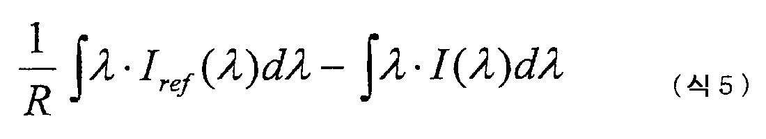
여기서, I(λ) 는, 흡수 효율 αq 를 구하는 대상으로 하고 있는 형광체 샘플을 장착하였을 때의, 반사 스펙트럼이다. (식 5) 의 적분 구간은 (식 4) 에서 정한 적분 구간과 동일하게 한다. 이와 같이 적분 구간을 한정함으로써, (식 5) 의 제 2 항은, 측정 대상으로 하고 있는 형광체 샘플이 여기광을 반사함으로써 발생한 포톤수에 대응한 것, 즉, 측정 대상으로 하고 있는 형광체 샘플로부터 발생하는 전체 포톤 중 형광 현상에서 유래되는 포톤을 제거한 것에 대응한 것이 된다. 실제의 스펙트럼 측정값은, 일반적으로는 λ 에 관한 어느 유한의 밴드폭으로 단락지은 디지털 데이터로서 얻어지기 때문에, (식 4) 및 (식 5) 의 적분은, 그 밴드폭에 기초한 합분에 의해 구해진다.Here, I (λ) is a reflection spectrum when the phosphor sample used as a target for obtaining the absorption efficiency αq is mounted. The integral section of (Equation 5) is the same as the integral section set in (Equation 4). By limiting the integration period in this manner, the second term in (Formula 5) corresponds to the number of photons generated by reflecting the excitation light of the phosphor sample to be measured, that is, generated from the phosphor sample to be measured. It corresponds to the thing which removed the photon derived from the fluorescent phenomenon among all the photons. Since actual spectral measurements are generally obtained as digital data separated by any finite bandwidth with respect to λ, the integration of (Equation 4) and (Equation 5) is determined by the sum based on the bandwidth. Become.
이상으로부터, αq = Nabs/N = (식 5)/(식 4) 로 구해진다.From the above, αq = N abs / N = (Expression 5) / (Expression 4).
다음으로, 내부 양자 효율 ηi 를 구하는 방법을 설명한다. ηi 는, 형광 현상에서 유래되는 포톤의 수 NPL 을 형광체 샘플이 흡수한 포톤의 수 Nabs 로 나눈 값이다.Next, a method of obtaining the internal quantum efficiency η i will be described. η i is a value obtained by dividing the number N PL of photons derived from the fluorescent phenomenon by the number N abs of photons absorbed by the phosphor sample.
여기서, NPL 은, 하기 (식 6) 으로 구해지는 양에 비례한다.Here, N PL is proportional to the quantity calculated | required by following (formula 6).
![]()
![]()
이 때, 적분 구간은, 형광체 샘플의 형광 현상에서 유래되는 포톤이 갖는 파장 범위로 한정한다. 형광체 샘플로부터 반사된 포톤의 기여를 I(λ) 로부터 제거하기 위함이다. 구체적으로 (식 6) 의 적분 구간의 하한은, (식 4) 의 적분 구간의 상단을 취하고, 상한은, 형광에서 유래되는 포톤을 포함하는 데에 필요 충분한 범위로 한다.At this time, the integration section is limited to the wavelength range of the photons derived from the fluorescent phenomenon of the phosphor sample. This is to remove the contribution of photons reflected from the phosphor sample from I (λ). Specifically, the lower limit of the integration section of (Equation 6) takes the upper end of the integration section of (Equation 4), and the upper limit is a sufficient range necessary to include photons derived from fluorescence.
이상에 의해, 내부 양자 효율 ηi 는, ηi = (식 6)/(식 5) 로 구해진다.By the above, internal quantum efficiency (eta) i is calculated | required by (eta) i (Formula 6) / (Formula 5).
또한, 디지털 데이터가 된 스펙트럼으로부터 적분을 실시하는 것에 관해서는, 흡수 효율 αq 를 구한 경우와 동일하다.Incidentally, the integration is performed from the spectrum of the digital data as in the case of obtaining the absorption efficiency αq.
그리고, 상기와 같이 하여 구한 흡수 효율 αq 와 내부 양자 효율 ηi 의 곱 을 취함으로써 외부 양자 효율 ηo 를 구한다. 혹은, ηo = (식 6)/(식 4) 의 관계로부터 구할 수도 있다. ηo 는, 형광에서 유래되는 포톤의 수 NPL 을 여기광의 전체 포톤수 N 으로 나눈 값이다.And the external quantum efficiency (eta) o is calculated | required by taking the product of the absorption efficiency (alpha) q calculated as mentioned above, and the internal quantum efficiency (eta) i. Or it can also be calculated | required from the relationship of (eta) = (expression 6) / (
[1-3. 복합 산질화물 형광체의 제조 방법][1-3. Method for producing complex oxynitride phosphor]
본 발명의 형광체를 얻기 위한 원료, 형광체 제조법 등에 대해서는 이하와 같다.The raw material, phosphor manufacturing method, etc. for obtaining the phosphor of this invention are as follows.
본 발명의 형광체의 제조 방법은 특별히 제한되지 않지만, 예를 들어, 상기 일반식 (I) 에 있어서의, 부활 원소인 원소 M1 의 원료 (이하 적절히「M1 원」이라고 한다), Ba 의 원료 (이하 적절히「Ba 원」이라고 한다), 금속 원소 M2 의 원료 (이하 적절히「M2 원」이라고 한다) 및 L 의 원료 (이하 적절히「L 원」이라고 한다) 를 혼합하고 (혼합 공정), 얻어진 혼합물을 소성함 (소성 공정) 으로써 제조할 수 있다.Although the manufacturing method of the fluorescent substance of this invention is not specifically limited, For example, the raw material of the element M1 which is an activating element in the said General formula (I) (henceforth "M1 member" suitably), and the raw material of Ba (hereinafter Suitably referred to as "Ba circle"), the raw material of the metal element M2 (hereinafter referred to as "M2 circle" suitably), and the raw material of L (hereinafter referred to as "L circle" suitably) are mixed (mixing process), and the obtained mixture is mixed It can manufacture by a hardening | curing (baking process).
[1-3-1. 형광체 원료][1-3-1. Phosphor raw material]
본 발명의 형광체의 제조에 사용되는 형광체 원료 (즉, M1 원, Ba 원, M2 원 및 L 원) 로는, M1, Ba, M2 및 L 의 각 원소의 금속, 합금, 이미드 화합물, 산질화물, 질화물, 산화물, 수산화물, 탄산염, 질산염, 황산염, 옥살산염, 카르복실산염, 할로겐화물 등을 들 수 있다. 이들 화합물 중에서, 복합 산질화물에 대한 반응성이나, 소성시에 있어서의 NOx, SOx 등의 발생량의 낮음 등을 고려하여, 적절히 선택하면 된다.Examples of the phosphor raw material (i.e., M1 source, Ba source, M2 source, and L source) used in the production of the phosphor of the present invention include metals, alloys, imide compounds, oxynitrides of M1, Ba, M2, and L, Nitrides, oxides, hydroxides, carbonates, nitrates, sulfates, oxalates, carboxylates, halides and the like. Among these compounds, in view of the reactivity and, NO x, low in amount of SO x, etc., such as at the time of firing of the composite oxynitride, may be suitably selected.
상기 M1 원 중, Eu 원의 구체예로는, Eu2O3, Eu2(SO4)3, Eu2(C2O4)3·10H2O, EuCl2, EuCl3, Eu(NO3)3·6H2O, EuN, EuNH 등을 들 수 있다. 그 중에서도 Eu2O3, EuCl2 등이 바람직하고, 특히 바람직하게는 Eu2O3 이다.In the M1 member, specific examples of the Eu member include Eu 2 O 3 , Eu 2 (SO 4 ) 3 , Eu 2 (C 2 O 4 ) 3 · 10H 2 O, EuCl 2 , EuCl 3 , and Eu (NO 3) ) 3 .6H 2 O, EuN, EuNH, and the like. Among them is Eu 2 O 3, EuCl 2, etc. are preferred, and particularly preferably from Eu 2 O 3.
또, Sm 원, Tm 원, Yb 원 등의 그 밖의 부활제 원소의 원료의 구체예로는, Eu 원의 구체예로서 제시한 각 화합물에 있어서, Eu 를 각각 Sm, Tm, Yb 등으로 치환한 화합물을 들 수 있다.Moreover, as a specific example of the raw material of other activator elements, such as Sm circle, Tm circle, and Yb circle, in each compound shown as a specific example of Eu circle, Eu was substituted by Sm, Tm, Yb, etc., respectively. The compound can be mentioned.
상기 Ba 원의 구체예로는, BaO, Ba(OH)2·8H2O, BaCO3, Ba(NO3)2, BaSO4, Ba(C2O4), Ba(OCOCH3)2, BaCl2, Ba3N2, BaNH 등을 들 수 있다. 이 중 바람직하게는, 탄산염, 산화물 등을 사용할 수 있지만, 산화물은 공기 중의 수분과 반응하기 쉽기 때문에, 취급면에서 탄산염이 보다 바람직하다. 그 중에서도, BaCO3 이 바람직하다. 공기 중의 안정성이 양호하고, 또, 가열에 의해 용이하게 분해되기 때문에, 목적 외의 원소가 잔류하기 어렵고, 또한, 고순도의 원료를 입수하기 쉽기 때문이다. 탄산염을 원료로 하는 경우에는, 미리 탄산염을 예비 소성하여 원료로서 사용하는 것이 바람직하다.Specific examples of the Ba source include BaO, Ba (OH) 2 · 8H 2 O, BaCO 3 , Ba (NO 3 ) 2 , BaSO 4 , Ba (C 2 O 4 ), Ba (OCOCH 3 ) 2 , BaCl 2, and the like Ba 3 N 2, BaNH. Of these, carbonates, oxides and the like can be preferably used. However, carbonates are more preferable in terms of handling because oxides are likely to react with moisture in the air. Especially, BaCO 3 is preferable. It is because stability in air is favorable and since it decompose | disassembles easily by heating, an element other than the objective is hard to remain and it is easy to obtain a high purity raw material. When using a carbonate as a raw material, it is preferable to pre-calculate the carbonate beforehand and use it as a raw material.
상기 M2 원으로서의 Sr 원의 구체예로는, SrO, Sr(OH)2·8H2O, SrCO3, Sr(NO3)2, SrSO4, Sr(C2O4)·H2O, Sr(OCOCH3)2·0.5H2O, SrCl2, Sr3N2, SrNH 등을 들 수 있다. 그 중에서도, SrCO3 이 바람직하다. 공기 중의 안정성이 양호하고, 또, 가열에 의해 용이하게 분해되어, 목적 외의 원소가 잔류하기 어렵고, 또한, 고순도의 원료를 입수하기 쉽기 때문이다.Specific examples of the Sr source as the M2 source include SrO, Sr (OH) 2 8H 2 O, SrCO 3 , Sr (NO 3 ) 2 , SrSO 4 , Sr (C 2 O 4 ) · H 2 O, Sr (OCOCH 3 ) 2 .0.5H 2 O, SrCl 2 , Sr 3 N 2 , SrNH, and the like. Especially, SrCO 3 is preferable. It is because stability in air is favorable, and it decompose | disassembles easily by heating, it is hard to remain an element other than a target, and it is easy to obtain a high purity raw material.
Mg 원의 구체예로는, MgO, Mg(OH)2, 염기성 탄산마그네슘 (mMgCO3·Mg(OH)2·nH2O), Mg(NO3)2·6H2O, MgSO4, Mg(C2O4)·2H2O, Mg(OCOCH3)2·4H2O, MgCl2, Mg3N2, MgNH 등을 들 수 있다. 그 중에서도, MgO 나 염기성 탄산마그네슘이 바람직하다.Specific examples of the Mg source include MgO, Mg (OH) 2 , basic magnesium carbonate (mMgCO 3 · Mg (OH) 2 · nH 2 O), Mg (NO 3 ) 2 .6H 2 O, MgSO 4 , Mg ( C 2 O 4) · and the like 2H 2 O, Mg (OCOCH 3 ) 2 · 4H 2 O,
Ca 원의 구체예로는, CaO, Ca(OH)2, CaCO3, Ca(NO3)2·4H2O, CaSO4·2H2O, Ca(C2O4)·H2O, Ca(OCOCH3)2·H2O, CaCl2, Ca3N2, CaNH 등을 들 수 있다. 그 중에서도, CaCO3, CaCl2 등이 바람직하다.Specific examples of Ca source include CaO, Ca (OH) 2 , CaCO 3 , Ca (NO 3 ) 2 .4H 2 O, CaSO 4 .2H 2 O, Ca (C 2 O 4 ) .H 2 O, Ca (OCOCH 3 ) 2 H 2 O, CaCl 2 , Ca 3 N 2 , CaNH and the like. Of these, such as CaCO 3, CaCl 2 is preferred.
Zn 원의 구체예로는, ZnO, ZnF2, ZnCl2, Zn(OH)2, Zn3N2, ZnNH 등의 아연 화합물 (단, 수화물이어도 된다) 을 들 수 있다. 그 중에서도, 입자 성장을 촉진시키는 효과가 높다는 관점에서 ZnF2·4H2O (단, 무수물이어도 된다) 등이 바람직하다.Specific examples of the Zn source, there may be mentioned zinc compounds such as ZnO, ZnF 2, ZnCl 2, Zn (OH) 2, Zn 3
또, M2 로서 탄산염을 원료로 하는 경우에는, 미리 탄산염을 예비 소성하여 원료로서 사용하는 것이 바람직하다.Moreover, when using carbonate as a raw material as M2, it is preferable to pre-calculate a carbonate beforehand and use it as a raw material.
상기 L 원 중, Si 원 화합물로는, SiO2 또는 Si3N4 를 사용하는 것이 바람직하다. 또, SiO2 가 되는 화합물을 사용할 수도 있다. 이와 같은 화합물로는, 구체적으로는, SiO2, H4SiO4, Si(OCOCH3)4 등을 들 수 있다. 또, Si3N4 로서 반응성면에서, 입경이 작고, 발광 효율면에서 순도가 높은 것이 바람직하다. 또한, 발광 효율면에서는 α-Si3N4 보다 β-Si3N4 가 바람직하고, 특히 불순물인 탄소 원소의 함유 비율이 적은 편이 바람직하다. 탄소 함유의 비율은, 적으면 적을수록 바람직하지만, 통상 0.01 중량% 이상 함유되고, 통상 0.3 중량% 이하, 바람직하게는 0.1 중량% 이하, 보다 바람직하게는 0.05% 이하이다.As of the L source, Si source compound, it is preferred to use SiO 2 or Si 3 N 4. In addition, it is also possible to use a compound of the SiO 2. Specific examples of such a compound include SiO 2 , H 4 SiO 4 , Si (OCOCH 3 ) 4 , and the like. Further, Si 3 N 4 preferably has a small particle size in terms of reactivity and high purity in terms of luminous efficiency. Further, in the surface-emission efficiency and the α-Si 3 N 4 than the β-Si 3 N 4 preferred, and particularly it is preferable with less impurity content of the carbon element. Although the ratio of carbon content is so small that it is small, it is preferable, but it contains 0.01 weight% or more normally, and is normally 0.3 weight% or less, Preferably it is 0.1 weight% or less, More preferably, it is 0.05% or less.
또, Ge 원 화합물로는, GeO2 또는 Ge3N4 를 사용하는 것이 바람직하다. 또, GeO2 인 화합물을 사용할 수도 있다. 이와 같은 화합물로는, 구체적으로는, GeO2, Ge(OH)4, Ge(OCOCH3)4, GeCl4 등을 들 수 있다.Further, a Ge source compound, it is preferred to use GeO 2 or Ge 3 N 4. In addition, it is also possible to use a compound of GeO 2. With such compounds, specifically, GeO 2, and the like Ge (OH) 4, Ge ( OCOCH 3) 4,
그 밖의 L 원 화합물의 구체예로는, 상기 Si 원 또는 Ge 원의 구체예로서 제시한 각 화합물에 있어서, Si 나 Ge 를 각각 Ti, Zr, Hf 등으로 치환한 화합물을 들 수 있다.As a specific example of another L source compound, the compound which substituted Si and Ge with Ti, Zr, Hf etc. in each compound shown as a specific example of the said Si source or Ge source is mentioned.
상기 각종 형광체 원료에 있어서는, 순도가 높고, 보다 백색도가 높은 형광체 원료를 사용하는 것이 얻어지는 형광체의 발광 효율을 높이기 때문에 바람직하다. 구체적으로는, 380㎚ ∼ 780㎚ 의 파장 범위에 있어서의 반사율이 60% 이상, 바람직하게는 70% 이상, 보다 바람직하게는 80% 이상인 형광체 원료를 사용하는 것이 바람직하다. 특히, 본 발명의 형광체의 발광 피크 파장에 가까운 파장인 525㎚ 에 있어서, 그 형광체 원료의 반사율은 60% 이상인 것이 바람직하고, 보다 바람직하게는 70% 이상, 더욱 바람직하게는 80% 이상, 특히 바람직하게는 90% 이상이다.In the above various phosphor raw materials, it is preferable to use a phosphor raw material having high purity and higher whiteness in order to increase the luminous efficiency of the obtained phosphor. Specifically, it is preferable to use the phosphor raw material whose reflectance in the wavelength range of 380 nm-780 nm is 60% or more, Preferably it is 70% or more, More preferably, it is 80% or more. In particular, at 525 nm, which is a wavelength close to the emission peak wavelength of the phosphor of the present invention, the reflectance of the phosphor raw material is preferably 60% or more, more preferably 70% or more, even more preferably 80% or more, particularly preferably Preferably 90% or more.
또, 복수 있는 형광체 원료 중에서도, 특히 Si3N4 는 반사율이 높은 것을 사용하는 것이 바람직하다. 또, 당해 반사율을 만족하는 Si3N4 로는, 불순물로서 함유되어 있는 탄소의 양으로서, 통상 0.2 중량% 이하, 바람직하게는 0.1 중량% 이하, 보다 바람직하게는 0.05 중량% 이하, 더욱 바람직하게는 0.03 중량% 이하인 것이 바람직하다. 그 불순물 탄소량은 적으면 적을수록 바람직하지만, 통상 0.001 중량% 이상이다.Further, among the plurality of fluorescent substance that, in particular Si 3 N 4, it is preferable to use the high reflectance. As Si 3 N 4 that satisfies the reflectance, the amount of carbon contained as an impurity is usually 0.2% by weight or less, preferably 0.1% by weight or less, more preferably 0.05% by weight or less, and further preferably It is preferable that it is 0.03 weight% or less. The smaller the amount of the impurity carbon is, the more preferable, but is usually 0.001% by weight or more.
이와 같은 반사율은, 반사 스펙트럼 측정을 실시하면 되고, 그 측정 방법으로는, 전술한 흡수 효율, 내부 양자 효율 및 외부 양자 효율의 설명의 항에서 기재한 것과 동일한 방법을 취하면 된다.Such reflectance may be performed by measuring the reflection spectrum, and the measuring method may be the same as that described in the above description of the absorption efficiency, the internal quantum efficiency, and the external quantum efficiency.
또한, 상기 서술한 M1 원, Ba 원, M2 원 및 L 원은, 각각, 1 종만을 사용해도 되고, 2 종 이상을 임의의 조합 및 비율로 병용해도 된다.In addition, only 1 type may be used for the above-mentioned M1 circle, Ba circle, M2 circle, and L circle, respectively, and may use 2 or more types together by arbitrary combinations and a ratio.
[1-3-2. 형광체의 제조 방법:혼합 공정][1-3-2. Manufacturing method of phosphor: Mixing process]
목적 조성이 얻어지도록 형광체 원료를 칭량하고, 볼 밀 등을 사용하여 충분히 혼합한 후, 도가니에 충전하고, 소정 온도, 분위기하에서 소성하고, 소성물을 분쇄, 세정함으로써, 본 발명의 형광체를 얻을 수 있다.The phosphor of the present invention can be obtained by weighing a phosphor raw material so as to obtain a desired composition, mixing it sufficiently using a ball mill or the like, filling it in a crucible, firing under a predetermined temperature and atmosphere, and pulverizing and washing the fired product. have.
상기 혼합 수법으로는, 특별히 한정은 되지 않지만, 구체적으로는, 하기 (A) 및 (B) 의 수법을 들 수 있다.Although it does not specifically limit as said mixing method, Specifically, the method of following (A) and (B) is mentioned.
(A) 예를 들어 해머 밀, 롤 밀, 볼 밀, 제트 밀 등의 건식 분쇄기, 또는, 막자사발과 막자 등을 사용하는 분쇄와, 예를 들어 리본 블렌더, V 형 블렌더, 헨셀 믹서 등의 혼합기, 또는, 막자사발과 막자를 사용하는 혼합을 조합하여, 전술한 형광체 원료를 분쇄 혼합하는 건식 혼합법.(A) For example, a dry mill such as a hammer mill, a roll mill, a ball mill, a jet mill, or a mill using a mortar and pestle, and a mixer such as a ribbon blender, a V-type blender, a Henschel mixer, or the like. Or dry mixing method which grind | mixes and mixes the above-mentioned fluorescent substance raw material by combining mixing using a mortar and pestle.
(B) 전술한 형광체 원료에 물 등의 용매 또는 분산매를 첨가하고, 예를 들어 분쇄기, 막자사발과 막자, 또는 증발 접시와 교반봉 등을 사용하여 혼합하고, 용액 또는 슬러리 상태로 한 다음, 분무 건조, 가열 건조, 또는 자연 건조 등에 의해 건조시키는 습식 혼합법.(B) A solvent or a dispersion medium such as water is added to the above-mentioned phosphor raw material, and mixed using, for example, a grinder, a mortar and pestle, an evaporating dish and a stirring rod, and brought into a solution or slurry state, and then sprayed. Wet mixing method which dries by drying, heat drying, or natural drying.
형광체 원료의 혼합은, 상기 습식 또는 건식 중 어느 것이어도 되지만, 물 또는 에탄올을 사용한 습식 혼합이 보다 바람직하다.The mixing of the phosphor raw material may be either wet or dry, but wet mixing using water or ethanol is more preferred.
[1-3-3. 형광체의 제조 방법:소성 공정][1-3-3. Manufacturing method of phosphor: firing process]
얻어진 혼합물을, 각 형광체 원료와 반응성이 낮은 재료로 이루어지는 도가니 또는 트레이 등의 내열 용기 중에 충전한다. 이와 같은 소성시에 사용하는 내열 용기의 재질로는, 예를 들어, 알루미나, 석영, 질화붕소, 질화규소, 탄화규소, 마그네슘, 멀라이트 등의 세라믹스, 백금, 몰리브덴, 텅스텐, 탄탈, 니오브, 이리듐, 로듐 등의 금속, 혹은, 그것들을 주성분으로 하는 합금, 카본 (그라파이트) 등을 들 수 있다. 여기서, 석영제의 내열 용기는, 비교적 저온, 즉, 1200℃ 이하에서의 열처리에 사용할 수 있고, 바람직한 사용 온도 범위는 1000℃ 이하이다.The obtained mixture is filled in a heat-resistant container such as a crucible or a tray made of a material having low reactivity with each phosphor raw material. As a material of the heat-resistant container used at the time of baking, for example, ceramics, such as alumina, quartz, boron nitride, silicon nitride, silicon carbide, magnesium, a mullite, platinum, molybdenum, tungsten, tantalum, niobium, iridium, Metals, such as rhodium, or the alloy which has them as a main component, carbon (graphite), etc. are mentioned. Here, the heat-resistant container made of quartz can be used for heat treatment at relatively low temperature, that is, 1200 degrees C or less, and a preferable use temperature range is 1000 degrees C or less.
이와 같은 내열 용기의 예로서, 바람직하게는 질화붕소제, 알루미나제, 질화규소제, 탄화규소제, 백금제, 몰리브덴제, 텅스텐제, 탄탈제의 내열 용기를 들 수 있다.As an example of such a heat resistant container, Preferably, the heat resistant container of a boron nitride agent, an alumina agent, a silicon nitride agent, a silicon carbide agent, a platinum agent, a molybdenum agent, a tungsten agent, and a tantalum agent is mentioned.
소성 공정에 대해서는, 통상, 1600℃ 를 초과하는 소성 온도에서는 소성분이 소결되어, 발광 강도가 낮아지는 경우가 있지만, 1400℃ 전후의 소성 온도에서는 결정성이 양호한 분체가 얻어진다. 따라서, 본 발명의 형광체를 제조하기 위한, 소성 온도로는, 통상 1000℃ 이상, 바람직하게는 1100℃ 이상, 보다 바람직하게는 1200℃ 이상의 온도이고, 또, 통상 1600℃ 이하, 바람직하게는 1500℃ 이하, 보다 바람직하게는 1450℃ 이하의 온도이다.About a baking process, a small component may sinter at the baking temperature exceeding 1600 degreeC normally, and light emission intensity may fall, but the powder with favorable crystallinity is obtained at the baking temperature around 1400 degreeC. Therefore, the firing temperature for producing the phosphor of the present invention is usually 1000 ° C or higher, preferably 1100 ° C or higher, more preferably 1200 ° C or higher, and usually 1600 ° C or lower, preferably 1500 ° C. Hereinafter, More preferably, it is the temperature of 1450 degrees C or less.
소성 분위기로는 특별히 제한되지 않지만, 통상, 불활성 가스 분위기 또는 환원 분위기하에서 실시된다. 여기서, 전술한 바와 같이, 부활 원소의 가수로는, 2 가인 것이 많은 편이 바람직하기 때문에, 환원 분위기인 것이 바람직하다. 또한, 불활성 가스 및 환원성 가스는, 1 종만을 사용해도 되고, 2 종 이상을 임의의 조합 및 비율로 병용해도 된다.Although it does not restrict | limit especially as a baking atmosphere, Usually, it is implemented in inert gas atmosphere or reducing atmosphere. Here, as mentioned above, since it is more preferable that the valence of an activation element is bivalent, it is preferable that it is a reducing atmosphere. In addition, only 1 type may be used for an inert gas and a reducing gas, and may use 2 or more types together by arbitrary combinations and a ratio.
불활성 가스 및 환원성 가스로는, 예를 들어, 일산화탄소, 수소, 질소, 아르곤 등을 들 수 있다. 이 중, 질소 가스 분위기하인 것이 바람직하고, 보다 바람직하게는 수소 가스 함유 질소 가스 분위기하이다. 상기 질소 (N2) 가스로는, 순도 99.9% 이상을 사용하는 것이 바람직하다. 수소 함유 질소를 사용하는 경우, 전기로 내의 산소 농도를 20ppm 이하로 낮추는 것이 바람직하다. 또한, 분위기 중의 수소 함유량은 1 체적% 이상이 바람직하고, 2 체적% 이상이 더욱 바람직하고, 또, 5 체적% 이하가 바람직하다. 분위기 중의 수소의 함유량은, 지나치게 높으면 안전성이 저하될 가능성이 있고, 지나치게 낮으면 충분한 환원 분위기 를 달성할 수 없을 가능성이 있기 때문이다.As inert gas and reducing gas, carbon monoxide, hydrogen, nitrogen, argon etc. are mentioned, for example. It is preferable that it is in nitrogen gas atmosphere among these, More preferably, it is in hydrogen gas containing nitrogen gas atmosphere. The nitrogen (N 2) gas, it is preferred to use a purity of 99.9%. When using hydrogen containing nitrogen, it is preferable to reduce the oxygen concentration in an electric furnace to 20 ppm or less. Moreover, 1 volume% or more is preferable, as for hydrogen content in atmosphere, 2 volume% or more is more preferable, Moreover, 5 volume% or less is preferable. This is because if the content of hydrogen in the atmosphere is too high, the safety may be lowered, and if it is too low, a sufficient reducing atmosphere may not be achieved.
또, 소성 시간은, 소성시의 온도나 압력 등에 따라서도 상이한데, 통상, 0.5 시간 이상, 바람직하게는 1 시간 이상이다. 또, 소성 시간은 긴 편이 좋지만, 통상, 100 시간 이하, 바람직하게는 50 시간 이하, 보다 바람직하게는 24 시간 이하, 더욱 바람직하게는 12 시간 이하이다.Moreover, although baking time changes also with temperature, pressure, etc. at the time of baking, it is 0.5 hours or more normally, Preferably it is 1 hour or more. In addition, the longer the firing time is, the longer it is, usually 100 hours or less, preferably 50 hours or less, more preferably 24 hours or less, and still more preferably 12 hours or less.
소성시의 압력은, 소성 온도 등에 따라서도 상이하기 때문에 특별히 한정되지 않지만, 통상 1 × 10⁻⁵Pa 이상, 바람직하게는 1 × 10⁻³Pa 이상, 보다 바람직하게는 0.01MPa 이상, 더욱 바람직하게는 0.1MPa 이상이고, 또, 상한으로는, 통상 5GPa 이하, 바람직하게는 1Gpa 이하, 보다 바람직하게는 200MPa 이하, 더욱 바람직하게는 100MPa 이하이다. 이 중, 공업적으로는 대기압 ∼ 1MPa 정도가 비용 및 수고면에서 간편하여 바람직하다.Although the pressure at the time of baking differs also according to baking temperature etc., it is not specifically limited, Usually, it is 1 * 10 <-5> Pa or more, Preferably it is 1 * 10 <-3> Pa or more, More preferably, it is 0.01 Mpa or more, More preferably, Is 0.1 MPa or more, and as an upper limit, it is usually 5 GPa or less, preferably 1 Gpa or less, more preferably 200 MPa or less, still more preferably 100 MPa or less. Among these, industrially, atmospheric pressure-about 1 MPa are preferable because they are simple in terms of cost and labor.
[1-3-4. 플럭스][1-3-4. Flux]
소성 공정에 있어서는, 양호한 결정을 성장시키는 관점에서, 반응계에 플럭스를 공존시켜도 된다. 플럭스의 종류는 특별히 제한되지 않지만, 예로는, NH4Cl, NH4F·HF 등의 할로겐화 암모늄;NaCO3, LiCO3 등의 알칼리 금속 탄산염;LiCl, NaCl, KCl, CsCl, LiF, NaF, KF, CsF 등의 알칼리 금속 할로겐화물;CaCl2, BaCl2, SrCl2, CaF2, BaF2, SrF2 등의 알칼리 토금속 할로겐화물;CaO, SrO, BaO 등의 알칼리 토금속 산화물;B2O3, H3BO3, NaB4O7 등의 붕소 산화물, 붕산 및 붕산염 화 합물;Li3PO4, NH4H2PO4 등의 인산염 화합물;AlF3 등의 할로겐화 알루미늄;ZnCl2, ZnF2 와 같은 할로겐화 아연, 산화아연, 황화아연 등의 아연 화합물;Bi2O3 등의 주기표 제 15 족 원소 화합물;Li3N, Ca3N2, Sr3N2, Ba3N2, BN 등등의 알칼리 금속, 알칼리 토금속 또는 제 13 족 원소의 질화물 등을 들 수 있다. 이 중 바람직하게는 할로겐화물이고, 이 중에서도, 알칼리 금속 할로겐화물, 알칼리 토금속 할로겐화물, Zn 의 할로겐화물이 바람직하다. 또, 이들 할로겐화물 중에서도, 불화물, 염화물이 바람직하다.In the firing step, from the viewpoint of growing good crystals, flux may coexist in the reaction system. The kind of flux is not particularly limited, but examples include ammonium halides such as NH 4 Cl and NH 4 FHF; alkali metal carbonates such as NaCO 3 and LiCO 3 ; LiCl, NaCl, KCl, CsCl, LiF, NaF, KF , an alkali metal halide such as CsF; CaCl 2, BaCl 2,
플럭스의 사용량은, 원료의 종류나 플럭스의 재료 등에 따라서도 상이한데, 통상 0.01 중량% 이상, 바람직하게는 0.1 중량% 이상, 보다 바람직하게는 1 중량% 이상, 또, 통상 20 중량% 이하, 나아가서는 10 중량% 이하의 범위가 바람직하다. 플럭스의 사용량이 지나치게 적으면, 플럭스의 효과가 나타나지 않고, 플럭스의 사용량이 지나치게 많으면, 플럭스 효과가 포화되거나, 모체 결정에 취입되어 발광색을 변화시키거나, 휘도 저하를 일으키는 경우가 있다. 이들 플럭스는 1 종을 단독으로 사용해도 되고, 2 종 이상을 임의의 조합 및 비율로 병용해도 된다.The amount of flux used varies depending on the type of raw material, the material of the flux, and the like, but is usually 0.01% by weight or more, preferably 0.1% by weight or more, more preferably 1% by weight or more, and usually 20% by weight or less. The range of 10 weight% or less is preferable. When the amount of flux used is too small, the effect of flux does not appear, and when the amount of flux is used too much, the flux effect may be saturated or may be blown into the mother crystal to change the emission color or cause a decrease in luminance. These fluxes may be used individually by 1 type, and may use 2 or more types together by arbitrary combinations and a ratio.
[1-3-5. 1 차 소성 및 2 차 소성][1-3-5. Primary firing and secondary firing]
또한, 소성 공정을 1 차 소성과 2 차 소성으로 분할하고, 혼합 공정에 의해 얻어진 원료 혼합물을 먼저 1 차 소성한 후, 볼 밀 등으로 다시 분쇄하고 나서 2 차 소성을 실시해도 된다.In addition, the firing step may be divided into primary firing and secondary firing, and the raw material mixture obtained by the mixing step may first be calcined, and then secondary firing may be performed after grinding again with a ball mill or the like.
1 차 소성의 온도는, 본 발명의 효과를 현저하게 해치지 않는 한 임의인데, 통상 800℃ 이상, 바람직하게는 1000℃ 이상, 또, 통상 1600℃ 이하, 바람직하게는 1400℃ 이하, 보다 바람직하게는 1300℃ 이하의 범위이다.Although the temperature of primary baking is arbitrary, unless the effect of this invention is remarkably impaired, it is 800 degreeC or more normally, Preferably it is 1000 degreeC or more, Moreover, it is 1600 degrees C or less normally, Preferably it is 1400 degrees C or less, More preferably, It is the range of 1300 degrees C or less.
여기서, 입도가 정돈된 형광체를 얻기 위해서는, 1 차 소성 온도를 낮게 설정하여 분체 상태에서 고상 반응을 진행시키는 것이 바람직하다. 한편, 고휘도의 형광체를 얻기 위해서는, 1 차 소성 온도를 높게 설정하여 용융 상태에서 원료가 충분히 혼합되어 반응한 후에 2 차 소성으로 결정 성장시키는 것이 바람직하다.Herein, in order to obtain a phosphor having an ordered particle size, it is preferable to set the primary firing temperature to a low level and to advance the solid phase reaction in the powder state. On the other hand, in order to obtain a high luminance phosphor, it is preferable to set the primary firing temperature high, and to crystally grow by secondary firing after the raw materials are sufficiently mixed and reacted in the molten state.
1 차 소성의 시간은, 본 발명의 효과를 현저하게 해치지 않는 한 임의인데, 통상 1 시간 이상, 바람직하게는 2 시간 이상, 또, 통상 100 시간 이하, 바람직하게는 50 시간 이하, 보다 바람직하게는 24 시간 이하, 더욱 바람직하게는 12 시간 이하이다.Although the time of primary baking is arbitrary, unless the effect of this invention is remarkably impaired, it is 1 hour or more normally, Preferably it is 2 hours or more, and also it is 100 hours or less normally, Preferably it is 50 hours or less, More preferably, 24 hours or less, More preferably, it is 12 hours or less.
2 차 소성의 온도, 시간 등의 조건은, 기본적으로 상기 서술한 소성 공정의 란에 기재한 조건과 동일하다.The conditions, such as temperature and time of secondary baking, are basically the same as the conditions described in the column of the baking process mentioned above.
또한, 플럭스는 1 차 소성 전에 혼합해도 되고, 2 차 소성 전에 혼합해도 된다. 또, 분위기 등의 소성 조건도 1 차 소성과 2 차 소성으로 변경해도 된다.In addition, the flux may be mixed before primary firing or may be mixed before secondary firing. Moreover, you may change baking conditions, such as atmosphere, to primary baking and secondary baking.
[1-3-6. 후처리][1-3-6. After treatment]
상기 서술한 소성 공정의 가열 처리 후에는, 필요에 따라, 세정, 건조, 분쇄, 분급 처리 등이 이루어진다.After heat processing of the above-mentioned baking process, washing | cleaning, drying, grinding | pulverization, classification processing, etc. are performed as needed.
분쇄 처리에는, 예를 들어, 원료의 혼합 공정에 사용할 수 있다고 하여 열거한 분쇄기를 사용할 수 있다.For the pulverization treatment, for example, a pulverizer listed as being usable for a raw material mixing step can be used.
세정은, 예를 들어, 탈이온수 등의 물, 에탄올 등의 유기 용제, 암모니아수 등의 알칼리성 수용액 등으로 실시할 수 있다. 또, 사용된 플럭스를 제거하는 등의 목적을 위해, 예를 들어, 염산, 질산, 황산 등의 무기산;또는, 아세트산 등의 유기산의 수용액을 사용할 수도 있다. 이 경우, 산성 수용액 중에서 세정 처리한 후에, 물로 다시 세정하는 것이 바람직하다.Washing can be performed, for example with water, such as deionized water, organic solvents, such as ethanol, and alkaline aqueous solutions, such as aqueous ammonia. In addition, for the purpose of removing the used flux, for example, an inorganic acid such as hydrochloric acid, nitric acid or sulfuric acid; or an aqueous solution of an organic acid such as acetic acid may be used. In this case, it is preferable to wash | clean again with water after wash | cleaning process in acidic aqueous solution.
분급 처리는, 예를 들어, 물체질을 실시하거나, 혹은, 각종 기류 분급기나 진동체 등 각종 분급기를 사용함으로써 실시할 수 있다. 그 중에서도, 나일론 메시에 의한 건식 분급을 사용하면, 중량 메디안 직경 20㎛ 정도의 분산성이 양호한 형광체를 얻을 수 있다.A classification process can be performed by performing object quality, for example, or using various classifiers, such as various airflow classifiers and a vibrating body. Especially, when dry classification by a nylon mesh is used, the fluorescent substance with favorable dispersibility about 20 micrometers in weight median diameter can be obtained.
또한, 얻어진 본 발명의 형광체를 사용하여, 후술하는 방법으로 발광 장치를 제조할 때에는, 내습성 등의 내후성을 한층 더 향상시키기 위해, 또는 후술하는 발광 장치의 형광체 함유부에 있어서의 수지에 대한 분산성을 향상시키기 위해 필요에 따라, 형광체의 표면을 상이한 물질로 피복하는 등의 표면 처리를 실시해도 된다.In addition, when manufacturing the light emitting device by the method mentioned later using the obtained fluorescent substance of this invention, in order to further improve weather resistance, such as moisture resistance, or to resin in the fluorescent substance containing part of the light emitting device mentioned later In order to improve acidity, you may surface-treat, such as coat | covering the surface of fluorescent substance with a different substance as needed.
형광체의 표면에 존재시킬 수 있는 물질 (이하, 임의로「표면 처리 물질」이라고 칭한다) 로는, 예를 들어, 유기 화합물, 무기 화합물 및 유리 재료 등을 들 수 있다.As a substance (henceforth called a "surface treatment substance") which can exist on the surface of fluorescent substance, an organic compound, an inorganic compound, a glass material, etc. are mentioned, for example.
유기 화합물로는, 예를 들어, 아크릴 수지, 폴리카보네이트, 폴리아미드, 폴리에틸렌 등의 열용융성 폴리머, 라텍스, 폴리오르가노실록산 등을 들 수 있다.As an organic compound, thermomeltable polymers, such as an acrylic resin, polycarbonate, a polyamide, polyethylene, latex, polyorganosiloxane, etc. are mentioned, for example.
무기 화합물로는, 예를 들어, 산화마그네슘, 산화알루미늄, 산화규소, 산화 티탄, 산화지르코늄, 산화주석, 산화게르마늄, 산화탄탈, 산화니오브, 산화바나듐, 산화붕소, 산화안티몬, 산화아연, 산화이트륨, 산화비스무트 등의 금속 산화물, 질화규소, 질화알루미늄 등의 금속 질화물, 인산칼슘, 인산바륨, 인산스트론튬 등의 오르토인산염, 폴리인산염을 들 수 있다.Examples of the inorganic compound include magnesium oxide, aluminum oxide, silicon oxide, titanium oxide, zirconium oxide, tin oxide, germanium oxide, tantalum oxide, niobium oxide, vanadium oxide, boron oxide, antimony oxide, zinc oxide, and yttrium oxide. And metal oxides such as bismuth oxide, metal nitrides such as silicon nitride and aluminum nitride, orthophosphates such as calcium phosphate, barium phosphate and strontium phosphate, and polyphosphates.
유리 재료로는, 예를 들어 붕규산염, 포스포규산염, 알칼리 규산염 등을 들 수 있다.As a glass material, borosilicate, phosphosilicate, an alkali silicate etc. are mentioned, for example.
이들 표면 처리 물질은, 1 종만을 사용해도 되고, 2 종 이상을 임의의 조합 및 비율로 병용해도 된다.These surface treatment substances may use only 1 type, and may use 2 or more types together by arbitrary combinations and a ratio.
상기의 표면 처리에 의해 얻어지는 본 발명의 형광체는, 표면 처리 물질의 존재가 전제이지만, 그 양태는, 예를 들어 하기의 것을 들 수 있다.Although the fluorescent substance of this invention obtained by said surface treatment presupposes presence of a surface treatment substance, the aspect is mentioned below, for example.
(i) 상기 표면 처리 물질이 연속막을 구성하여 형광체 표면을 피복하는 양태.(i) An aspect in which the surface treatment material forms a continuous film to cover the surface of the phosphor.
(ii) 상기 표면 처리 물질이 다수의 미립자가 되어, 형광체의 표면에 부착함으로써 형광체 표면을 피복하는 양태.(ii) An aspect in which the surface treatment material becomes a plurality of fine particles and covers the surface of the phosphor by adhering to the surface of the phosphor.
형광체의 표면에 대한 표면 처리 물질의 부착량 내지 피복량은, 본 발명의 효과를 현저하게 해치지 않는 한 임의인데, 형광체의 중량에 대해, 통상 0.1 중량% 이상, 바람직하게는 1 중량% 이상, 보다 바람직하게는 5 중량% 이상, 더욱 바람직하게는 10 중량% 이상이고, 통상 50 중량% 이하, 바람직하게는 30 중량% 이하, 보다 바람직하게는 20 중량% 이하이다. 형광체에 대한 표면 처리 물질량이 지나치게 많으면 형광체의 발광 특성이 저해되는 경우가 있고, 지나치게 적으면 표면 피복이 불완전해져, 내습성, 분산성의 개선이 보이지 않는 경우가 있다.The amount of coating or coating amount of the surface treatment material on the surface of the phosphor is arbitrary unless the effect of the present invention is significantly impaired, but is usually 0.1% by weight or more, preferably 1% by weight or more, based on the weight of the phosphor. Preferably it is 5 weight% or more, More preferably, it is 10 weight% or more, Usually 50 weight% or less, Preferably it is 30 weight% or less, More preferably, it is 20 weight% or less. When the amount of the surface treatment substance to the phosphor is too large, the luminescence properties of the phosphor may be impaired. When the amount of the surface treatment material is too small, the surface coating may be incomplete and improvement in moisture resistance and dispersibility may not be observed.
또, 표면 처리에 의해 형성되는 표면 처리 물질의 막두께 (층두께) 는, 본 발명의 효과를 현저하게 해치지 않는 한 임의인데, 통상 10㎚ 이상, 바람직하게는 50㎚ 이상이고, 통상 2000㎚ 이하, 바람직하게는 1000㎚ 이하이다. 이 막두께가 지나치게 두꺼우면 형광체의 발광 특성이 저해되는 경우가 있고, 지나치게 얇으면 표면 피복이 불완전해져, 내습성, 분산성의 개선이 보이지 않는 경우가 있다.In addition, the film thickness (layer thickness) of the surface treatment material formed by surface treatment is arbitrary, unless the effect of this invention is remarkably impaired, Usually it is 10 nm or more, Preferably it is 50 nm or more, and is normally 2000 nm or less Preferably it is 1000 nm or less. If the film thickness is too thick, the luminescence properties of the phosphor may be impaired. If the film thickness is too thin, surface coating may be incomplete, and improvement of moisture resistance and dispersibility may not be observed.
표면 처리의 방법에는 특별히 한정은 없지만, 예를 들어 하기와 같은 금속 산화물 (산화규소) 에 의한 피복 처리법을 들 수 있다.Although there is no limitation in particular in the method of surface treatment, For example, the coating method with the following metal oxide (silicon oxide) is mentioned.
본 발명의 형광체를 에탄올 등의 알코올 중에 혼합하여, 교반하고, 다시 암모니아수 등의 알칼리 수용액을 혼합하여, 교반한다. 다음으로, 가수분해 가능한 알킬규산에스테르, 예를 들어 테트라에틸오르토규산을 혼합하여, 교반한다. 얻어진 용액을 3 분간 ∼ 60 분간 정치 (靜置) 한 후, 스포이드 등에 의해 형광체 표면에 부착되지 않은 산화규소 입자를 포함하는 상청을 제거한다. 이어서, 알코올 혼합, 교반, 정치, 상청 제거를 수회 반복한 후, 120℃ ∼ 150℃ 에서 10 분 ∼ 5 시간, 예를 들어 2 시간의 감압 건조 공정을 거쳐, 표면 처리 형광체를 얻는다.The fluorescent substance of this invention is mixed in alcohol, such as ethanol, and stirred, Then, aqueous alkali solution, such as aqueous ammonia, is mixed and stirred. Next, a hydrolyzable alkyl silicate ester, for example, tetraethylorthosilicate, is mixed and stirred. After leaving the obtained solution for 3 minutes to 60 minutes, the supernatant containing silicon oxide particles which do not adhere to the surface of the phosphor by a dropper or the like is removed. Subsequently, after repeating alcohol mixing, stirring, standing, and removing the supernatant several times, the surface-treated fluorescent substance is obtained through the pressure reduction drying process of 10 minutes-5 hours, for example, 2 hours at 120 degreeC-150 degreeC.
형광체의 표면 처리 방법으로는, 이 외에, 예를 들어 구형의 산화규소 미분을 형광체에 부착시키는 방법 (일본 공개특허공보 평2-209989호, 일본 공개특허공보 평2-233794호), 형광체에 규소계 화합물의 피막을 부착시키는 방법 (일본 공개특허공보 평3-231987호), 형광체 미립자의 표면을 폴리머 미립자로 피복하는 방법 (일본 공개특허공보 평6-314593호), 형광체를 유기 재료, 무기 재료 및 유리 재료 등으로 코팅하는 방법 (일본 공개특허공보 2002-223008호), 형광체의 표면을 화학 기상 반응법에 의해 피복하는 방법 (일본 공개특허공보 2005-82788호), 금속 화합물의 입자를 부착시키는 방법 (일본 공개특허공보 2006-28458호) 등의 공지된 방법을 사용할 수 있다.As the surface treatment method of the phosphor, besides, for example, a method of attaching spherical silicon oxide fine powder to the phosphor (Japanese Patent Laid-Open No. 2-209989, Japanese Patent Laid-Open No. 2-233794), A method of attaching a coating of a sub-system compound (Japanese Patent Laid-Open No. 3-231987), a method of coating the surface of phosphor microparticles with polymer microparticles (Japanese Patent Laid-Open No. 6-314593), an organic material and an inorganic material And a method of coating with a glass material (Japanese Laid-Open Patent Publication No. 2002-223008), a method of coating the surface of a phosphor by a chemical vapor phase reaction method (Japanese Patent Laid-Open No. 2005-82788), and attaching particles of a metal compound. Known methods, such as the method (Unexamined-Japanese-Patent No. 2006-28458), can be used.
[1-3-7. 합금법에 의한 제조][1-3-7. Manufacture by Alloy Method]
또, 본 발명의 형광체를 얻기 위해서, 상기의 원료 및 제조법 이외에, 합금을 원료로 하는 제조법을 적용할 수 있다.Moreover, in order to obtain the fluorescent substance of this invention, the manufacturing method which uses an alloy as a raw material other than said raw material and manufacturing method can be applied.
공업적으로 널리 사용되고 있는 금속 단체의 정제 방법에는, 승화 정제, 플로우팅존법, 증류법 등이 알려져 있다. 이와 같이 금속 단체는 화합물에 비해 정제가 용이해지는 원소가 많이 존재한다. 따라서 형광체를 제조하는 데에 있어서 필요한 금속 원소 단체를 출발 원료로 하는 편이 화합물을 원료로 하는 방법보다 순도가 높은 원료를 얻기 쉬운 점에서 우수하다.Sublimation refining, the floating zone method, the distillation method, etc. are known as the refine | purification method of the single metal which is widely used industrially. As such, there are many elements in the metal single substance that are easier to be purified than the compounds. Therefore, it is excellent in the point which makes it easy to obtain a raw material with high purity rather than the method which uses a compound as a starting material as the starting material of the elemental metal element which is necessary for manufacturing a fluorescent substance.
또, 부활제 원소의 결정 격자 내에서의 균일 분산이라는 관점에 있어서도 구성 원소가 되는 원료가 금속 단체이면 이들을 융해시켜 합금으로 함으로써, 부활제 원소를 용이하게 균일 분포시킬 수 있다.Moreover, also in the viewpoint of the uniform dispersion in the crystal lattice of an activator element, if the raw material which becomes a constituent element is a metal single substance, it can melt | dissolve and make it an alloy, and can uniformly distribute an activator element easily.
이상의 관점에서 목적으로 하는 형광체를 구성하는 금속 원소를 함유하는 합금, 바람직하게는 목적으로 하는 형광체를 구성하는 금속 원소 전부를 함유하는 합금을 출발 원료로 하여, 형광체를 제조함으로써, 고성능인 형광체를 공업적으로 생산할 수 있다.In view of the above, an alloy containing a metal element constituting the target phosphor, preferably an alloy containing all the metal elements constituting the target phosphor, is prepared as a starting material, thereby producing a high performance phosphor. Can be produced as
종래부터, Si 와 알칼리 토금속을 포함하는 합금으로는, Ca7Si, Ca2Si, Ca5Si3, CaSi, Ca2Si2, Ca14Si19, Ca3Si4, SrSi, SrSi2, Sr4Si7, Sr5Si3, Sr7Si 가 알려져 있고, Si, 알루미늄, 알칼리 토금속을 포함하는 합금은, Ca(Si1 - xAlx)2, Sr(Si1 -xAlx)2, Ba(Si1 - xAlx)2, Ca1 - xSrx(Si1 - yAly)2 등이 알려져 있지만, 그 중에서도, A(B0.5Si0.5)2:(A = Ca,Sr,Ba:B = Al,Ga) 는 초전도 특성에 관해, 일본 공개특허공보 2005-54182호, M. Imai, Applied Physics Letters, 80(2002)1019-1021, M. Imai, Physical Review B, 68, (2003), 064512 등에 있어서 검토가 실시되고 있다.Conventionally, alloys containing Si and alkaline earth metals include Ca 7 Si, Ca 2 Si, Ca 5 Si 3 , CaSi, Ca 2 Si 2 , Ca 14 Si 19 , Ca 3 Si 4 , SrSi, SrSi 2 , Sr 4 Si 7 , Sr 5 Si 3 , and Sr 7 Si are known, and alloys containing Si, aluminum, and alkaline earth metals include Ca (Si 1 - x Al x ) 2 , Sr (Si 1 -x Al x ) 2 , Ba (Si 1 - x Al x ) 2 , Ca 1 - x Sr x (Si 1 - y Al y ) 2, and the like are known, but among them, A (B 0.5 Si 0.5 ) 2 : (A = Ca, Sr, Ba: B = Al, Ga) is described in Japanese Unexamined Patent Publication No. 2005-54182, M. Imai, Applied Physics Letters, 80 (2002) 1019-1021, M. Imai, Physical Review B, 68, ( 2003), 064512, etc., examination is performed.
본 발명에 있어서는, 융해 방법으로서, 상기 Si 와 알칼리 토류를 포함하는 합금에 대한 공지된 융해 방법, 예를 들어 아크 융해, 고주파 융해법을 사용할 수 있다.In the present invention, as the melting method, a known melting method for the alloy containing Si and alkaline earth, for example, arc melting and high frequency melting can be used.
또, 원료 합금은 괴상 그대로는 형광체화하는 반응이 거의 진행되지 않기 때문에, 분쇄 공정에 의해 소정의 입경으로 하는 것이 바람직하다. 바람직한 입경 범위는, 통상 1㎛ 이상 500㎛ 이하이다. 만일 합금에 불균일 부분이 있어도 이 분쇄 공정에 의해 매크로로는 균질화될 뿐이지만, 미크로로 보면 분쇄된 입자가 상이한 조성인 것은 바람직한 상태는 아니다. 따라서 합금 전체가 균질인 것이 바람직하다.In addition, since the raw material alloy hardly proceeds to phosphoratize as it is, it is preferable to set it as predetermined particle diameter by a grinding | pulverization process. Preferable particle size range is 1 micrometer or more and 500 micrometers or less normally. Even if there is a non-uniform portion in the alloy, it is only homogenized in the macro by this grinding step, but in micro, it is not a preferable state that the ground particles are of different composition. Therefore, it is preferable that the whole alloy is homogeneous.
이와 같이 하여 얻어진 합금 분말을 충전한 도가니 혹은 트레이를, 분위기 제어가 가능한 가열로에 넣은 후, 질소를 포함하는 가스를 유통시켜 계내를 충분히 이 가스로 치환한다. 필요에 따라, 계내를 진공 배기한 후, 가스를 유통시켜도 된다. 산질화물의 제조는 질소 및 산소의 혼합 가스를 사용할 수 있다.The crucible or tray filled with the alloy powder thus obtained is placed in a heating furnace capable of controlling the atmosphere, and then a gas containing nitrogen is passed through to completely replace the system with this gas. As needed, after evacuating the inside of a system, you may make gas flow. The preparation of oxynitrides may use a mixed gas of nitrogen and oxygen.
상기의 합금 분말은, 40% 이하의 체적 충전율로 유지한 상태에서 소성하는 것이 바람직하다. 또한, 체적 충전율은, (혼합 분말의 부피 밀도)/(혼합 분말의 이론 밀도) × 100[%] 에 의해 구할 수 있다. 용기로는, 금속 화합물과의 반응성이 낮은 점에서, 질화붕소 소결체가 적합하다.It is preferable to bake the said alloy powder in the state hold | maintained at 40% or less of volume filling rate. In addition, a volume filling rate can be calculated | required by (volume density of mixed powder) / (theoretical density of mixed powder) x 100 [%]. As the container, a boron nitride sintered compact is suitable in view of low reactivity with the metal compound.
금속의 질화 반응은, 통상 발열 반응이다. 원료로서 금속 합금을 사용한 경우 고려해야 할 것은, 급격하게 방출되는 반응열에 의해 원료 합금이 다시 융해되어, 표면적이 감소되기 때문에, 기체 질소와의 반응을 지연시키는 것이다. 따라서, 원료 합금이 융해되지 않는 반응 속도를 유지하는 것이, 고성능의 형광체를 안정적으로 제조할 수 있기 때문에 바람직하다.The nitriding reaction of the metal is usually an exothermic reaction. In the case of using a metal alloy as a raw material, consideration should be given to delaying the reaction with gaseous nitrogen because the raw material alloy is melted again by the rapidly released heat of reaction and the surface area is reduced. Therefore, it is preferable to maintain the reaction rate at which the raw material alloy does not melt because it is possible to stably produce high-performance phosphors.
[1-4. 복합 산질화물 형광체의 용도]1-4. Use of complex oxynitride phosphors]
본 발명의 형광체는, 형광체를 사용하는 임의의 용도에 사용할 수 있는데, 특히, 청색 광 또는 근자외광으로 여기 가능하다는 특성을 살려, 각종 발광 장치 (예를 들어, 후술하는「본 발명의 제 1, 제 2 및 제 3 발광 장치」) 에 바람직하게 사용할 수 있다. 조합하는 형광체의 종류나 사용 비율을 조정함으로써, 다양한 발광색의 발광 장치를 제조할 수 있다. 특히, 본 발명의 형광체가 녹색 형광체인 점에서, 청색 광을 발하는 여기 광원과 주황색 내지 적색의 형광을 발하는 형광체 (주황색 내지 적색 형광체) 를 조합하면, 백색 발광 장치를 제조할 수 있다. 이 경우의 발광색은, 본 발명의 형광체나 녹색 형광체의 발광 파장을 조정함으로 써, 기호의 발광색으로 할 수 있지만, 예를 들어, 이른바 의사 백색 (예를 들어, 청색 LED 와 황색의 형광을 발하는 형광체 (황색 형광체) 를 조합한 발광 장치의 발광색) 의 발광 스펙트럼과 유사한 발광 스펙트럼을 얻을 수도 있다. 또한, 이 백색 발광 장치에 적색의 형광을 발하는 형광체 (적색 형광체) 를 조합하면, 적색의 연색성이 매우 우수한 발광 장치나 전구색 (따뜻함이 있는 백색) 으로 발광하는 발광 장치를 실현할 수 있다. 또, 근자외광을 발하는 여기 광원에, 본 발명의 형광체와, 청색의 형광을 발하는 형광체 (청색 형광체) 및 적색 형광체를 조합하여도, 백색 발광 장치를 제조할 수 있다.Although the fluorescent substance of this invention can be used for arbitrary uses using a fluorescent substance, various light-emitting devices (for example, "the 1st, Second and third light emitting devices). By adjusting the type and use ratio of the phosphors to be combined, light emitting devices of various emission colors can be manufactured. In particular, since the phosphor of the present invention is a green phosphor, a white light emitting device can be manufactured by combining an excitation light source emitting blue light and a phosphor emitting orange to red fluorescence (orange to red phosphor). In this case, the emission color of the present invention can be the desired emission color by adjusting the emission wavelength of the phosphor of the present invention or the green phosphor, but is, for example, a so-called pseudo white (e.g., a phosphor emitting blue and yellow fluorescence). A light emission spectrum similar to the light emission spectrum of (light emission color of a light emitting device combining yellow phosphor) can be obtained. In addition, by combining red fluorescent material (red phosphor) with this white light emitting device, it is possible to realize a light emitting device which is excellent in red color rendering property or a light emitting device which emits light in a bulb color (warm white). In addition, a white light emitting device can be produced by combining the phosphor of the present invention with the phosphor of the present invention, the phosphor emitting blue fluorescence (blue phosphor) and the red phosphor.
발광 장치의 발광색으로는 백색에 제한되지 않고, 필요에 따라, 황색 형광체 (황색의 형광을 발하는 형광체), 청색 형광체, 주황색 내지 적색 형광체, 다른 종류의 녹색 형광체 등을 조합하여, 형광체의 종류나 사용 비율을 조정함으로써, 임의의 색으로 발광하는 발광 장치를 제조할 수 있다. 이렇게 하여 얻어진 발광 장치를, 화상 표시 장치의 발광부 (특히 액정용 백라이트 등) 나 조명 장치로서 사용할 수 있다.The light emitting color of the light emitting device is not limited to white, and if necessary, a type or use of a phosphor by combining a yellow phosphor (phosphor that emits yellow fluorescence), blue phosphor, orange to red phosphor, and other kinds of green phosphors By adjusting the ratio, a light emitting device that emits light in any color can be manufactured. The light emitting device thus obtained can be used as a light emitting portion (especially a backlight for liquid crystal) or an illuminating device of the image display device.
[2. 형광체 함유 조성물][2. Phosphor-containing composition]
본 발명의 형광체는, 액체 매체와 혼합하여 사용할 수도 있다. 특히, 본 발명의 형광체를 발광 장치 등의 용도에 사용하는 경우에는, 이것을 액체 매체 중에 분산시킨 형태로 사용하는 것이 바람직하다. 본 발명의 형광체를 액체 매체 중에 분산시킨 것을, 적절히「본 발명의 형광체 함유 조성물」이라고 부르는 것으로 한다.The fluorescent substance of this invention can also be used in mixture with a liquid medium. In particular, when the phosphor of the present invention is used in a light emitting device or the like, it is preferable to use the phosphor in a form dispersed in a liquid medium. What disperse | distributed the fluorescent substance of this invention in a liquid medium shall be called "the fluorescent substance containing composition of this invention" suitably.
[2-1. 형광체][2-1. Phosphor]
본 발명의 형광체 함유 조성물에 함유시키는 본 발명의 형광체의 종류에 제한은 없고, 상기 서술한 것으로부터 임의로 선택할 수 있다. 또, 본 발명의 형광체 함유 조성물에 함유시키는 본 발명의 형광체는, 1 종만이어도 되고, 2 종 이상을 임의의 조합 및 비율로 병용해도 된다.There is no restriction | limiting in the kind of fluorescent substance of this invention contained in the fluorescent substance containing composition of this invention, It can select arbitrarily from the above-mentioned thing. Moreover, only 1 type may be sufficient as the fluorescent substance of this invention to be contained in the fluorescent substance containing composition of this invention, and may use 2 or more types together by arbitrary combinations and a ratio.
또한, 본 발명의 형광체 함유 조성물에는, 본 발명의 효과를 현저하게 해치지 않는 한, 본 발명의 형광체 이외의 형광체를 함유시켜도 된다.The phosphor-containing composition of the present invention may contain phosphors other than the phosphor of the present invention so long as the effects of the present invention are not significantly impaired.
[2-2. 액체 매체][2-2. Liquid medium]
본 발명의 형광체 함유 조성물에 사용되는 액체 매체로는, 그 형광체의 성능을 목적의 범위에서 해치지 않는 한에 있어서 특별히 한정되지 않는다. 예를 들어, 원하는 사용 조건하에 있어서 액상의 성질을 나타내고, 본 발명의 형광체를 바람직하게 분산시킴과 함께, 바람직하지 않은 반응을 일으키지 않는 것이면, 임의의 무기계 재료 및/또는 유기계 재료를 사용할 수 있다.The liquid medium used for the phosphor-containing composition of the present invention is not particularly limited as long as the performance of the phosphor is not impaired within the intended range. For example, any inorganic material and / or organic material can be used as long as it exhibits liquid phase properties under desired use conditions, preferably disperses the phosphor of the present invention, and does not cause undesirable reactions.
무기계 재료로는, 예를 들어, 금속 알콕시드, 세라믹 전구체 폴리머 혹은 금속 알콕시드를 함유하는 용액을 졸-겔법에 의해 가수분해 중합하여 이루어지는 용액, 또는 이들의 조합을 고화한 무기계 재료 (예를 들어 실록산 결합을 갖는 무기계 재료) 등을 들 수 있다.As an inorganic material, For example, the inorganic material which solidified the solution formed by hydrolysis-polymerizing the solution containing a metal alkoxide, a ceramic precursor polymer, or a metal alkoxide by the sol-gel method, or a combination thereof (for example, Inorganic materials having a siloxane bond); and the like.
유기계 재료로는, 예를 들어, 열가소성 수지, 열경화성 수지, 광경화성 수지 등을 들 수 있다. 구체적으로는, 예를 들어, 폴리메타아크릴산메틸 등의 메타아크릴 수지;폴리스티렌, 스티렌-아크릴로니트릴 공중합체 등의 스티렌 수지;폴 리카보네이트 수지;폴리에스테르 수지;페녹시 수지;부티랄 수지;폴리비닐알코올;에틸셀룰로오스, 셀룰로오스아세테이트, 셀룰로오스아세테이트부틸레이트 등의 셀룰로오스계 수지;에폭시 수지;페놀 수지;실리콘 수지 등을 들 수 있다.As an organic type material, a thermoplastic resin, a thermosetting resin, a photocurable resin, etc. are mentioned, for example. Specifically, For example, methacryl resins, such as polymethyl methacrylate; Styrene resin, such as a polystyrene and a styrene acrylonitrile copolymer; Polycarbonate resin; Polyester resin; Phenoxy resin; Butyral resin; Poly Vinyl alcohol; cellulose resins such as ethyl cellulose, cellulose acetate and cellulose acetate butyrate; epoxy resins; phenol resins; silicone resins;
이들 중에서 특히 조명 등 대출력의 발광 장치에 형광체를 사용하는 경우에는, 내열성이나 내광성 등을 목적으로 하여 규소 함유 화합물을 사용하는 것이 바람직하다.Among them, in the case of using the phosphor in a high output light emitting device such as lighting, it is preferable to use a silicon-containing compound for the purpose of heat resistance, light resistance, and the like.
규소 함유 화합물이란 분자 중에 규소 원자를 갖는 화합물을 말하고, 예를 들어, 폴리오르가노실록산 등의 유기 재료 (실리콘계 재료), 산화규소, 질화규소, 산질화규소 등의 무기 재료 및 붕규산염, 포스포규산염, 알칼리 규산염 등의 유리 재료를 들 수 있다. 그 중에서도, 핸들링의 용이함 등의 면에서, 실리콘계 재료가 바람직하다.The silicon-containing compound refers to a compound having a silicon atom in a molecule, and for example, inorganic materials such as organic materials (silicon-based materials) such as polyorganosiloxanes, silicon oxides, silicon nitrides, and silicon oxynitrides, and borosilicates, phosphosilicates, Glass materials, such as alkali silicate, are mentioned. Among them, silicon-based materials are preferred in view of ease of handling and the like.
상기 실리콘계 재료란, 통상, 실록산 결합을 주쇄로 하는 유기 중합체를 말하고, 예를 들어 일반 조성식 (i) 로 나타내는 화합물 및/또는 그들의 혼합물을 들 수 있다.The said silicone type material means the organic polymer which has a siloxane bond as a principal chain normally, For example, the compound and / or mixture thereof represented by general composition formula (i) are mentioned.
(R1R2R3SiO1 /2)M(R4R5SiO2 /2)D(R6SiO3 /2)T(SiO4 /2)Q···식 (i) (R 1 R 2 R 3 SiO 1/2) M (R 4
일반 조성식 (i) 에 있어서, R1 내지 R6 은, 유기 관능기, 수산기, 수소 원자로 이루어지는 군에서 선택되는 것을 나타낸다. 또한, R1 내지 R6 은, 동일해도 되고, 상이해도 된다.In the general composition formula (i), R 1 to R 6 are, it indicates that the organic functional group selected from a hydroxyl group, a hydrogen atom the group consisting of. In addition, R <1> -R <6> may be the same and may differ.
또, 상기 식 (i) 에 있어서, M, D, T 및 Q 는, 각각 0 이상 1 미만이고, M + D + T + Q = 1 을 만족하는 수이다.In addition, in said formula (i), M, D, T, and Q are each 0 or more and less than 1, and are a number which satisfy | fills M + D + T + Q = 1.
그 실리콘계 재료는, 반도체 발광 소자의 밀봉에 사용하는 경우, 액상의 실리콘계 재료를 사용하여 밀봉한 후, 열이나 광에 의해 경화시켜 사용할 수 있다.When used for sealing a semiconductor light emitting element, the silicon-based material can be used by being cured by heat or light after sealing using a liquid silicon-based material.
실리콘계 재료를 경화의 메커니즘에 의해 분류하면, 통상, 부가 중합 경화 타입, 축중합 경화 타입, 자외선 경화 타입, 퍼옥사이드 가황 타입 등의 실리콘계 재료를 들 수 있다. 이들 중에서는, 부가 중합 경화 타입 (부가형 실리콘 수지), 축합 경화 타입 (축합형 실리콘 수지), 자외선 경화 타입이 바람직하다. 이하, 부가형 실리콘계 재료 및 축합형 실리콘계 재료에 대해 설명한다.When a silicone type material is classified by the mechanism of hardening, silicone type materials, such as an addition polymerization hardening type, a condensation polymerization hardening type, an ultraviolet curing type, a peroxide vulcanization type, are mentioned normally. In these, addition polymerization hardening type (addition type silicone resin), condensation hardening type (condensation type silicone resin), and ultraviolet curing type are preferable. Hereinafter, an addition type silicon type material and a condensation type silicon type material are demonstrated.
부가형 실리콘계 재료란, 폴리오르가노실록산 사슬이, 유기 부가 결합에 의해 가교된 것을 말한다. 대표적인 것으로는, 예를 들어 비닐실란과 히드로실란을 Pt 촉매 등의 부가형 촉매의 존재하 반응시켜 얻어지는 Si-C-C-Si 결합을 가교점에 갖는 화합물 등을 들 수 있다. 이들은 시판되고 있는 것을 사용할 수 있고, 예를 들어 부가 중합 경화 타입의 구체적 상품명으로는 신에츠 화학 공업사 제조「LPS-1400」「LPS-2410」「LPS-3400」등을 들 수 있다.An addition type silicone type material means that the polyorganosiloxane chain was bridge | crosslinked by the organic addition bond. As a typical example, the compound etc. which have Si-C-C-Si bond | crosslinking point obtained by making vinylsilane and hydrosilane react in presence of addition type catalysts, such as a Pt catalyst, etc. are mentioned. These can use a commercially available thing, For example, Shin-Etsu Chemical Co., Ltd. "LPS-1400", "LPS-2410", "LPS-3400", etc. are mentioned as a specific brand name of an addition polymerization hardening type.
한편, 축합형 실리콘계 재료란, 예를 들어, 알킬알콕시실란의 가수분해·중축합으로 얻어지는 Si-O-Si 결합을 가교점에 갖는 화합물을 들 수 있다.On the other hand, with a condensation type | system | group silicone material, the compound which has the Si-O-Si bond obtained by hydrolysis and polycondensation of an alkylalkoxy silane at a crosslinking point is mentioned, for example.
구체적으로는, 하기 일반식 (ii) 및/또는 (iii) 으로 나타내는 화합물 및/또는 그 올리고머를 가수분해·중축합하여 얻어지는 중축합물을 들 수 있다. 또한, 이들의 화합물 및/또는 그 올리고머는, 1 종만을 사용해도 되고, 2 종 이상을 임의의 조합 및 비율로 병용해도 된다.Specifically, the polycondensate obtained by hydrolyzing and polycondensing the compound represented by the following general formula (ii) and / or (iii) and / or its oligomer is mentioned. In addition, these compounds and / or its oligomers may use only 1 type, and may use 2 or more types together by arbitrary combinations and a ratio.
Mm +XnY1 m -n 일반식 (ii)M m + X n Y 1 m -n general formula (ii)
(일반식 (ii) 중, M 은, 규소, 알루미늄, 지르코늄 및 티탄에서 선택되는 적어도 1 종의 원소를 나타내고, X 는, 가수분해성기를 나타내고, Y1 은, 1 가의 유기 기를 나타내고, m 은, M 의 가수를 나타내는 1 이상의 정수를 나타내고, n 은, X 기의 수를 나타내는 1 이상의 정수를 나타낸다. 단, m ≥ n 이다)(In General Formula (ii), M represents at least one element selected from silicon, aluminum, zirconium and titanium, X represents a hydrolyzable group, Y 1 represents a monovalent organic group, and m is, One or more integers representing the valence of M, and n represents one or more integers representing the number of X groups, provided that m> n.)
(Ms +XtY1 s -t)uY2 일반식 (iii)(M s + X t Y 1 s -t ) u Y 2 General formula (iii)
(일반식 (iii) 중, M 은, 규소, 알루미늄, 지르코늄 및 티탄에서 선택되는 적어도 1 종의 원소를 나타내고, X 는, 가수분해성기를 나타내고, Y1 은, 1 가의 유기기를 나타내고, Y2 는, u 가의 유기기를 나타내고, s 는, M 의 가수를 나타내는 1 이상의 정수를 나타내고, t 는, 1 이상, s-1 이하의 정수를 나타내고, u 는, 2 이상의 정수를 나타낸다)(In General Formula (iii), M represents at least one element selected from silicon, aluminum, zirconium, and titanium, X represents a hydrolyzable group, Y 1 represents a monovalent organic group, and Y 2 is , u represents an organic group, s represents an integer of 1 or more indicating a valence of M, t represents an integer of 1 or more and s-1 or less, and u represents an integer of 2 or more)
또, 축합형 실리콘계 재료에는, 경화 촉매를 함유시켜도 된다. 이 경화 촉매로는, 예를 들어, 금속 킬레이트 화합물 등을 바람직한 것으로서 사용할 수 있다. 금속 킬레이트 화합물은, Ti, Ta, Zr 중 어느 1 이상을 포함하는 것이 바람직하고, Zr 을 포함하는 것이 더욱 바람직하다. 또한, 경화 촉매는, 1 종만을 사용해도 되고, 2 종 이상을 임의의 조합 및 비율로 병용해도 된다.In addition, the condensation type silicon-based material may contain a curing catalyst. As this curing catalyst, a metal chelate compound etc. can be used as a preferable thing, for example. It is preferable that a metal chelate compound contains any one or more of Ti, Ta, Zr, and it is more preferable that Zr is included. In addition, only 1 type may be used for a curing catalyst, and may use 2 or more types together by arbitrary combinations and a ratio.
이와 같은 축합형 실리콘계 재료로는, 예를 들어 일본 특허출원 2006-47274호 ∼ 47277호 명세서 및 일본 특허출원 2006-176468호 명세서에 기재된 반도체 발광 디바이스용 부재가 바람직하다.As such a condensation type | system | group silicon type material, the member for semiconductor light emitting devices described in Unexamined-Japanese-Patent No. 2006-47274-47277 specification, and Unexamined-Japanese-Patent No. 2006-176468 specification is preferable, for example.
축합형 실리콘계 재료 중에서, 특히 바람직한 재료에 대해, 이하에 설명한다.Among the condensed silicon-based materials, particularly preferred materials will be described below.
실리콘계 재료는, 일반적으로 반도체 발광 소자나 소자를 배치하는 기판, 패키지 등과의 접착성이 약한 것이 과제로 여겨지는데, 밀착성이 높은 실리콘계 재료로서, 특히, 이하의 특징 [5] ∼ [7] 중 하나 이상을 갖는 축합형 실리콘계 재료가 바람직하다.The silicon-based material is generally considered to have a weak adhesiveness with a semiconductor light emitting element, a substrate on which the element is placed, a package, and the like, and is a silicon-based material having high adhesion, and in particular, one of the following features [5] to [7] Condensed silicon-based materials having the above are preferable.
[5] 규소 함유율이 20 중량% 이상이다.[5] The silicon content is 20% by weight or more.
[6] 이후에 상세히 서술하는 방법에 의해 측정한 고체 Si-핵자기 공명 (NMR) 스펙트럼에 있어서, 하기 (a) 및/또는 (b) 의 Si 에서 유래되는 피크를 적어도 1 개 갖는다.[6] In the solid Si-nuclear magnetic resonance (NMR) spectrum measured by the method described in detail later, at least one peak derived from Si of the following (a) and / or (b) is included.
(a) 피크 탑의 위치가 테트라메톡시실란을 기준으로 하여 케미컬 시프트 -40ppm 이상, 0ppm 이하의 영역에 있고, 피크의 반값폭이 0.3ppm 이상, 3.0ppm 이하인 피크.(a) A peak whose position of the peak top is in the range of -40 ppm or more and 0 ppm or less based on tetramethoxysilane, and whose half value width of a peak is 0.3 ppm or more and 3.0 ppm or less.
(b) 피크 탑의 위치가 테트라메톡시실란을 기준으로 하여 케미컬 시프트 -80ppm 이상, -40ppm 미만의 영역에 있고, 피크의 반값폭이 0.3ppm 이상 5.0ppm 이하인 피크.(b) A peak whose position of the peak top is in the range of -80 ppm or more and less than -40 ppm of the chemical shift based on tetramethoxysilane, and the half value width of the peak is 0.3 ppm or more and 5.0 ppm or less.
[7] 실란올 함유율이 0.1 중량% 이상, 10 중량% 이하이다.[7] The silanol content is 0.1 wt% or more and 10 wt% or less.
본 발명에 있어서는, 상기의 특징 [5] ∼ [7] 중, 특징 [5] 를 갖는 실리콘계 재료가 바람직하다. 더욱 바람직하게는, 상기의 특징 [5] 및 [6] 을 갖는 실리콘계 재료가 바람직하다. 특히 바람직하게는, 상기의 특징 [5] ∼ [7] 을 모두 갖는 실리콘계 재료가 바람직하다. 이하, 상기의 특징 [5] ∼ [7] 에 대해 설명한다.In this invention, the silicone type material which has the characteristic [5] is preferable among said characteristics [5]-[7]. More preferably, a silicon-based material having the above-mentioned features [5] and [6] is preferable. Especially preferably, the silicone type material which has all said characteristics [5]-[7] is preferable. Hereinafter, the above-mentioned features [5] to [7] will be described.
[2-2-1. 특징 [5] (규소 함유율)]2-2-1. [5] (Silicone Content)]
본 발명에 바람직한 실리콘계 재료의 규소 함유율은, 통상 20 중량% 이상인데, 그 중에서도 25 중량% 이상이 바람직하고, 30 중량% 이상이 보다 바람직하다. 한편, 상한으로는, SiO2 만으로 이루어지는 유리의 규소 함유율이 47 중량% 라는 이유에서, 통상 47 중량% 이하의 범위이다.Although silicon content rate of the silicone-type material preferable for this invention is 20 weight% or more normally, 25 weight% or more is especially preferable, and 30 weight% or more is more preferable. On the other hand, the upper limit, the reason that in the silicon content of 47% by weight of a glass composed of only SiO 2, is usually the range of less than 47 wt%.
또한, 실리콘계 재료의 규소 함유율은, 예를 들어 이하의 방법을 사용하여 유도 결합 고주파 플라즈마 분광 (inductively coupled plasma spectrometry:이하 적절히「ICP」라고 약기한다) 분석을 실시하고, 그 결과에 기초하여 산출할 수 있다.In addition, the silicon content of a silicon-based material is analyzed by inductively coupled plasma spectrometry (hereinafter abbreviated as "ICP" appropriately) using the following method, and is calculated based on the result, for example. Can be.
{규소 함유율의 측정}{Measurement of silicon content rate}
실리콘계 재료를 백금 도가니 중에서 대기 중, 450℃ 에서 1 시간, 이어서 750℃ 에서 1 시간, 950℃ 에서 1.5 시간 유지하여 소성하고, 탄소 성분을 제거한 후, 얻어진 잔사 소량에 10 배량 이상의 탄산나트륨을 첨가하고 버너 가열하여 용융시키고, 이것을 냉각시켜 탈염수를 첨가하고, 다시 염산으로 pH 를 중성 정도로 조정하면서 규소로서 수 ppm 정도가 되도록 정용하여, ICP 분석을 실시한다.The silicon-based material is baked in a platinum crucible for 1 hour at 450 ° C., then 1 hour at 750 ° C. and 1.5 hours at 950 ° C., and then calcined. After removing the carbon component, 10 times or more of sodium carbonate is added to the obtained residue and burner It heats, melt | dissolves, this is cooled, demineralized water is added, and ICP analysis is performed, adjusting it to about several ppm as silicon, adjusting pH to neutrality with hydrochloric acid again.
[2-2-2. 특징 [6] (고체 Si-NMR 스펙트럼)][2-2-2. [6] (Solid Si-NMR Spectrum)
본 발명에 바람직한 실리콘계 재료의 고체 Si-NMR 스펙트럼을 측정하면, 유기기의 탄소 원자가 직접 결합된 규소 원자에서 유래되는 상기 (a) 및/또는 (b) 의 피크 영역에 적어도 1 개, 바람직하게는 복수개의 피크가 관측된다.When measuring the solid Si-NMR spectrum of a silicon-based material preferred in the present invention, at least one, preferably in the peak region of (a) and / or (b) derived from a silicon atom to which carbon atoms of an organic group are directly bonded A plurality of peaks are observed.
케미컬 시프트마다 정리하면, 본 발명에 바람직한 실리콘계 재료에 있어서, (a) 에 기재된 피크의 반값폭은, 분자 운동의 구속이 작기 때문에 전반적으로 후술하는 (b) 에 기재된 피크의 경우보다 작고, 통상 3.0ppm 이하, 바람직하게는 2.0ppm 이하, 또, 통상 0.3ppm 이상의 범위이다.In summary for each chemical shift, in the silicon-based material preferred in the present invention, the half-value width of the peak described in (a) is generally smaller than that of the peak described in (b) described later in general, because the constraint of molecular motion is small. It is a range of ppm or less, preferably 2.0 ppm or less, and usually 0.3 ppm or more.
한편, (b) 에 기재된 피크의 반값폭은, 통상 5.0ppm 이하, 바람직하게는 4.0ppm 이하, 또, 통상 0.3ppm 이상, 바람직하게는 0.4ppm 이상의 범위이다.On the other hand, the half-value width of the peak described in (b) is usually 5.0 ppm or less, preferably 4.0 ppm or less, and usually 0.3 ppm or more, preferably 0.4 ppm or more.
상기의 케미컬 시프트 영역에 있어서 관측되는 피크의 반값폭이 지나치게 크면, 분자 운동의 구속이 커 변형이 큰 상태가 되어, 크랙이 발생하기 쉽고, 내열·내후 내구성이 떨어지는 부재가 되는 경우가 있다. 예를 들어, 4 관능 실란을 다용한 경우나, 건조 공정에 있어서 급속한 건조를 실시하여 큰 내부 응력을 쌓은 상태 등에 있어서, 반값폭 범위가 상기의 범위보다 커진다.If the half-value width of the peak observed in the above chemical shift region is too large, the constraint of molecular motion is large and the deformation is large, and cracks are likely to occur, and the member may be inferior in heat resistance and weather resistance. For example, in the case where the tetrafunctional silane is used abundantly, or in a state where rapid drying is carried out in a drying step and a large internal stress is accumulated, the half-value width range is larger than the above range.
또, 피크의 반값폭이 지나치게 작으면, 그 환경에 있는 Si 원자는 실록산 가교에 관련되지 않게 되고, 3 관능 실란이 미가교 상태에서 잔류하는 예 등, 실록산 결합 주체로 형성되는 물질보다 내열·내후 내구성이 떨어지는 부재가 되는 경우가 있다.In addition, if the half width of the peak is too small, the Si atoms in the environment are not related to the siloxane crosslinking, and the heat resistance and weather resistance are higher than those of the substance formed by the siloxane bond, such as the trifunctional silane remaining in an uncrosslinked state. It may become a member with inferior durability.
단, 대량의 유기 성분 중에 소량의 Si 성분이 포함되는 실리콘계 재료에 있어서는, -80ppm 이상으로 상기 서술한 반값폭 범위의 피크가 확인되어도, 양호한 내열·내광성 및 도포 성능은 얻어지지 않는 경우가 있다.However, in the silicon-based material in which a small amount of Si component is contained in a large amount of organic components, even if the peak of the half value width range mentioned above is confirmed at -80 ppm or more, favorable heat resistance, light resistance, and application | coating performance may not be obtained.
본 발명에 바람직한 실리콘계 재료의 케미컬 시프트의 값은, 예를 들어 이하의 방법을 사용하여 고체 Si-NMR 측정을 실시하고, 그 결과에 기초하여 산출할 수 있다. 또, 측정 데이터의 해석 (반값폭이나 실란올량 해석) 은, 예를 들어 가우스 함수나 로렌츠 함수를 사용한 파형 분리 해석 등에 의해, 각 피크를 분할하여 추출하는 방법으로 실시한다.The value of the chemical shift of the silicon-based material preferred in the present invention can be calculated based on the result of performing solid Si-NMR measurement, for example, using the following method. In addition, analysis of the measurement data (half value width and silanol amount analysis) is performed by a method of dividing and extracting each peak by, for example, waveform separation analysis using a Gaussian function or Lorentz function.
{고체 Si-NMR 스펙트럼 측정 및 실란올 함유율의 산출}{Solid Si-NMR Spectral Measurement and Calculation of Silanol Content}
실리콘계 재료에 대해 고체 Si-NMR 스펙트럼을 실시하는 경우, 이하의 조건으로 고체 Si-NMR 스펙트럼 측정 및 파형 분리 해석을 실시한다. 또, 얻어진 파형 데이터로부터, 실리콘계 재료에 대해, 각각의 피크의 반값폭을 구한다. 또, 전체 피크 면적에 대한 실란올 유래의 피크 면적의 비율로부터, 전체 규소 원자 중의 실란올로 되어 있는 규소 원자의 비율 (%) 을 구하고, 별도로 분석한 규소 함유율과 비교함으로써 실란올 함유율을 구한다.When performing a solid Si-NMR spectrum with respect to a silicon type material, solid Si-NMR spectrum measurement and waveform separation analysis are performed on condition of the following. Moreover, the half value width of each peak is calculated | required with respect to a silicon type material from the obtained waveform data. Moreover, the silanol content rate is calculated | required by comparing the ratio (%) of the silicon atom which becomes the silanol in all the silicon atoms from the ratio of the peak area derived from silanol with respect to the total peak area, and comparing it with the silicon content rate analyzed separately.
{장치 조건}{Device conditions}
장치:Chemagnetics 사 Infinity CMX-400 핵자기 공명 분광 장치Device: Inmagnetic CMX-400 Nuclear Magnetic Resonance Spectroscopy
29Si 공명 주파수:79.436MHz29Si resonance frequency: 79.436MHz
프로브:7.5㎜φCP/MAS 용 프로브Probe: Probe for 7.5mmφCP / MAS
측정 온도:실온Measurement temperature: Room temperature
시료 회전수:4kHzSample rotation speed: 4kHz
측정법:싱글 펄스법Measurement method: Single pulse method
1H 디커플링 주파수:50kHz1H decoupling frequency: 50kHz
29Si 플립각:90˚29Si flip angle: 90 degrees
29Si90˚ 펄스폭:5.0㎲29Si90˚ pulse width: 5.0㎲
반복 시간:600sRepeat time: 600s
적산 횟수:128 회Number of integration: 128 times
관측폭:30kHzObservation width: 30kHz
브로드닝 팩터:20HzBroadcasting factor: 20Hz
기준 시료 : 테트라메톡시실란Reference Sample: Tetramethoxysilane
실리콘계 재료에 대해서는, 512 포인트를 측정 데이터로서 취입하고, 8192 포인트로 제로 필링하여 푸리에 변환한다.As for the silicon-based material, 512 points are taken in as measurement data, zero peeled to 8192 points, and Fourier transformed.
{파형 분리 해석법}{Waveform separation analysis}
푸리에 변환 후의 스펙트럼의 각 피크에 대해 로렌츠 파형 및 가우스 파형 혹은 양자의 혼합에 의해 작성한 피크 형상의 중심 위치, 높이, 반값폭을 가변 파라미터로 하고, 비선형 최소 이승법에 의해 최적화 계산을 실시한다.For each peak of the spectrum after the Fourier transform, the center position, height, and half-value width of the peak shape created by the Lorentz waveform, the Gaussian waveform, or a mixture of both are set as variable parameters, and optimization calculation is performed by a nonlinear least-squares method.
또한, 피크의 동정은, AIChE Journal, 44(5), p.1141, 1998년 등을 참고로 한다.In addition, the identification of the peak is referred to AIChE Journal, 44 (5), p. 1141, 1998 and the like.
[2-2-3. 특징 [7] (실란올 함유율)][2-2-3. [7] (Silanol Content)]
본 발명에 바람직한 실리콘계 재료는, 실란올 함유율이, 통상 0.1 중량% 이 상, 바람직하게는 0.3 중량% 이상, 또, 통상 10 중량% 이하, 바람직하게는 8 중량% 이하, 더욱 바람직하게는 5 중량% 이하의 범위이다. 실란올 함유율을 낮게 함으로써, 실란올계 재료는 시간 경과적 변화가 적고, 장기 성능 안정성이 우수하고, 흡습·투습성 모두 낮은 우수한 성능을 갖는다. 단, 실란올이 전혀 포함되지 않은 부재는 밀착성이 떨어지기 때문에, 실란올 함유율에 상기와 같이 최적인 범위가 존재한다.The silanol content of the present invention is preferably 0.1% by weight or more, preferably 0.3% by weight or more, and usually 10% by weight or less, preferably 8% by weight or less, and more preferably 5% by weight. It is the range of% or less. By lowering the silanol content, the silanol-based material is less likely to change over time, has excellent long-term performance stability, and has excellent performance with low moisture absorption and moisture permeability. However, since the adhesiveness is inferior to the member which contains no silanol at all, there exists an optimal range as mentioned above in silanol content rate.
또한, 실리콘계 재료의 실란올 함유율은, 예를 들어 [2-2-2. 특징 [6] (고체 Si-NMR 스펙트럼)] 의 {고체 Si-NMR 스펙트럼 측정 및 실란올 함유율의 산출} 의 항에 있어서 설명한 방법을 사용하여 고체 Si-NMR 스펙트럼 측정을 실시하고, 전체 피크 면적에 대한 실란올 유래의 피크 면적의 비율로부터, 전체 규소 원자 중의 실란올로 되어 있는 규소 원자의 비율 (%) 을 구하고, 별도로 분석한 규소 함유율과 비교함으로써 산출할 수 있다.In addition, the silanol content rate of a silicone type material is [2-2-2. The solid Si-NMR spectrum measurement was performed using the method described in the section of [solid Si-NMR spectrum measurement and calculation of silanol content rate] of [6] (Solid Si-NMR spectrum). From the ratio of the peak area derived from silanol, the ratio (%) of the silicon atom of silanol in all the silicon atoms can be calculated | required, and it can calculate by comparing with the silicon content rate analyzed separately.
또, 본 발명에 바람직한 실리콘계 재료는, 적당량의 실란올을 함유하고 있기 때문에, 통상적으로는, 디바이스 표면에 존재하는 극성 부분에 실란올이 수소 결합하여, 밀착성이 발현된다. 극성 부분으로는, 예를 들어, 수산기나 메탈록산 결합의 산소 등을 들 수 있다.Moreover, since the silicon-based material suitable for the present invention contains an appropriate amount of silanol, the silanol is usually hydrogen bonded to the polar portion present on the surface of the device, and the adhesiveness is expressed. As a polar part, oxygen of a hydroxyl group, a metal siloxane bond, etc. are mentioned, for example.
또, 본 발명에 바람직한 실리콘계 재료는, 통상, 적당한 촉매의 존재하에서 가열함으로써, 디바이스 표면의 수산기와의 사이에 탈수 축합에 의한 공유 결합을 형성하여, 더욱 강고한 밀착성을 발현할 수 있다.In addition, the silicon-based material preferable in the present invention can form covalent bonds by dehydration condensation between hydroxyl groups on the surface of the device by heating in the presence of a suitable catalyst, and can express more firm adhesiveness.
한편, 실란올이 지나치게 많으면, 계내가 증점 (增粘) 되어 도포가 곤란해지 거나, 활성이 높아져 가열에 의해 경비분이 휘발되기 전에 고화됨으로써, 발포나 내부 응력의 증대가 발생하여, 크랙 등을 야기하는 경우가 있다.On the other hand, when too much silanol is thickened in a system and it becomes difficult to apply | coat, or it becomes high and solidifies before a nasal component volatilizes by heating, foaming and an increase of internal stress arise, and it causes a crack etc. There is a case.
[2-2-4. 액체 매체의 함유율]2-2-4. Content of liquid medium]
액체 매체의 함유율은, 본 발명의 효과를 현저하게 해치지 않는 한 임의인데, 본 발명의 형광체 함유 조성물 전체에 대해, 통상 50 중량% 이상, 바람직하게는 75 중량% 이상이고, 통상 99 중량% 이하, 바람직하게는 95 중량% 이하이다. 액체 매체의 양이 많은 경우에는 특별한 문제는 일어나지 않지만, 반도체 발광 장치로 한 경우에 원하는 색도 좌표, 연색 지수, 발광 효율 등을 얻기 위해서는, 통상, 상기와 같은 배합 비율로 액체 매체를 사용하는 것이 바람직하다. 한편, 액체 매체가 지나치게 적으면 유동성이 없어 취급하기 어려워질 가능성이 있다.Although the content rate of a liquid medium is arbitrary, as long as the effect of this invention is not impaired remarkably, it is 50 weight% or more normally, Preferably it is 75 weight% or more with respect to the whole phosphor containing composition of this invention, Usually 99 weight% or less, Preferably it is 95 weight% or less. In the case where the amount of the liquid medium is large, no particular problem arises. However, in order to obtain desired chromaticity coordinates, color rendering index, luminous efficiency, etc. in the case of the semiconductor light emitting device, it is usually preferable to use the liquid medium in the above-mentioned mixing ratio. Do. On the other hand, when there are too few liquid media, there exists a possibility that it may become difficult to handle because there is no fluidity.
액체 매체는, 본 발명의 형광체 함유 조성물에 있어서, 주로 바인더로서의 역할을 갖는다. 액체 매체는, 1 종을 단독으로 사용해도 되지만, 2 종 이상을 임의의 조합 및 비율로 병용해도 된다. 예를 들어, 내열성이나 내광성 등을 목적으로 하여 규소 함유 화합물을 사용하는 경우에는, 당해 규소 함유 화합물의 내구성을 해치지 않을 정도로, 에폭시 수지 등 다른 열경화성 수지를 함유해도 된다. 이 경우, 다른 열경화성 수지의 함유량은, 통상, 바인더인 액체 매체 전체량에 대해 25 중량% 이하, 바람직하게는 10 중량% 이하이다.The liquid medium mainly serves as a binder in the phosphor-containing composition of the present invention. Although a liquid medium may be used individually by 1 type, you may use 2 or more types together by arbitrary combinations and a ratio. For example, when using a silicon containing compound for the purpose of heat resistance, light resistance, etc., you may contain other thermosetting resins, such as an epoxy resin, so that the durability of the said silicon containing compound may not be impaired. In this case, content of another thermosetting resin is 25 weight% or less with respect to the liquid medium whole quantity which is a binder normally, Preferably it is 10 weight% or less.
[2-3. 그 밖의 성분][2-3. Other ingredients]
또한, 본 발명의 형광체 함유 조성물에는, 본 발명의 효과를 현저하게 해치지 않는 한, 형광체 및 액체 매체 이외에, 그 밖의 성분을 함유시켜도 된다. 또, 그 밖의 성분은, 1 종만을 사용해도 되고, 2 종 이상을 임의의 조합 및 비율로 병용해도 된다.The phosphor-containing composition of the present invention may contain other components in addition to the phosphor and the liquid medium as long as the effects of the present invention are not significantly impaired. Moreover, only 1 type may be used for another component and it may use 2 or more types together by arbitrary combinations and a ratio.
[3. 발광 장치][3. Light emitting device]
[3-1. 제 1 발광 장치][3-1. First light emitting device]
본 발명의 제 1 발광 장치는, 여기 광원과, 여기 광원으로부터의 광의 조사하에서 녹색의 형광을 발하고, 또한, 하기 (1), (2) 및 (3) 의 특성을 갖는 형광체를 구비한다.The 1st light-emitting device of this invention is equipped with the fluorescent substance which emits green fluorescence under irradiation of the excitation light source and the light from an excitation light source, and has the characteristics of following (1), (2), and (3).
(1) 455㎚ 파장의 광을 조사한 경우의 20℃ 에서의 발광 스펙트럼도 중의 발광 피크 강도값에 대한 150℃ 에서의 발광 스펙트럼도 중의 발광 피크 강도값의 비율이 55% 이상이다.(1) The ratio of the emission peak intensity value in the emission spectrum diagram at 150 ° C. to the emission peak intensity value in the emission spectrum diagram at 20 ° C. when irradiated with light having a wavelength of 455 nm is 55% or more.
(2) 390㎚ 파장의 광을 조사한 경우의 발광 스펙트럼도 중의 발광 피크 강도값에 대한 410㎚ 파장의 광을 조사한 경우의 발광 스펙트럼도 중의 발광 피크 강도값의 비율이 90% 이상이다.(2) The ratio of the emission peak intensity value in the emission spectrum diagram when the light of 410 nm wavelength is irradiated with respect to the emission peak intensity value in the emission spectrum diagram when the light of 390 nm wavelength is irradiated is 90% or more.
(3) JIS Z8701 에 기초하는 형광체의 발광색의 색도 좌표값으로서 x ≤ 0.3, y ≥ 0.5 를 만족한다.(3) x≤0.3 and y≥0.5 are satisfied as chromaticity coordinate values of emission colors of phosphors based on JIS Z8701.
여기서, 여기 광원에 제한은 없고, 특성 (1) ∼ (3) 의 특성을 갖는 녹색 형광체를 여기할 수 있는 한, 임의의 것을 사용할 수 있다. 그 중에서도, 후술하는 제 1 발광체와 동일한 것이 바람직하다. 또한, 여기 광원은, 1 개를 단독으로 사용해도 되고, 2 개 이상을 임의의 조합 및 비율로 병용해도 된다.Here, there is no restriction | limiting in an excitation light source, Any thing can be used as long as the green fluorescent substance which has the characteristic of characteristics (1)-(3) can be excited. Especially, the same thing as the 1st light-emitting body mentioned later is preferable. In addition, an excitation light source may be used individually by 1 type, and may use 2 or more together by arbitrary combinations and a ratio.
또, 특성 (1) 에 대해서는 [1-2-2. 온도 특성] 에서 설명한 바와 같고, 특성 (2) 에 대해서는 [1-2-3. 여기 파장] 에서 설명한 바와 같고, 특성 (3) 에 대해서는 [1-2-4. 발광색] 에서 설명한 바와 같다.Moreover, about the characteristic (1), it is [1-2-2. Temperature characteristics] and the characteristics (2) for [1-2-3. Excitation wavelength], and for characteristics (3), [1-2-4. Light emission color].
본 발명의 제 1 발광 장치는, 여기 광원을 갖고, 또한, 상기 (1), (2) 및 (3) 의 특성을 갖는 녹색 형광체를 사용하고 있는 것 외에는, 공지된 장치 구성을 임의로 취하면 된다.The first light emitting device of the present invention may have a known device configuration, except that it has an excitation light source and uses a green phosphor having the characteristics of (1), (2) and (3). .
상기 (1), (2) 및 (3) 의 특성을 갖는 녹색 형광체를 사용함으로써, 승온에 의한 색 편차도 작고, 또, 근자외부터 청색 영역까지의 여기 광원에 대해, 안정적인 발광 효율을 나타내고, 나아가서는, 액정 디스플레이용 광원 등의 백색 발광 장치로서 사용한 경우에 디스플레이의 색 재현 범위가 넓어진다는 점에서 우수한 발광 장치를 실현할 수 있다.By using the green fluorescent substance which has the characteristics of said (1), (2), and (3), the color deviation by temperature rising is also small, and shows the stable luminous efficiency with respect to the excitation light source from near ultraviolet to a blue region, Further, when used as a white light emitting device such as a light source for a liquid crystal display, an excellent light emitting device can be realized in that the color reproduction range of the display is widened.
또한, 본 발명의 제 1 발광 장치에 사용하는 녹색 형광체는, 특성 (1) ∼ (3) 이외에도, [1-2-2. 온도 특성], [1-2-3. 여기 파장] 및 [1-2-4. 발광색] 에서 설명한 본 발명의 형광체와 동일한 특성을 갖는 것이 바람직하다.In addition, the green fluorescent substance used for the 1st light-emitting device of this invention, in addition to the characteristic (1)-(3), has [1-2-2. Temperature characteristic], [1-2-3. Excitation wavelength] and [1-2-4. It is preferable to have the same characteristics as the phosphor of the present invention described in [Emission Color].
또, 본 발명의 제 1 발광 장치에 사용하는 녹색 형광체는, 그 중량 메디안 직경에 대해서는, [1-2-7. 중량 메디안 직경] 의 항에서 본 발명의 형광체에 대해 설명한 것과 동일하다.Moreover, about the weight median diameter of the green fluorescent substance used for the 1st light-emitting device of this invention, it is [1-2-7. Weight median diameter] is the same as that described for the phosphor of the present invention.
또한, 본 발명의 제 1 발광 장치에 사용하는 녹색 형광체는, 그 내부 양자 효율, 흡수 효율 및 외부 양자 효율에 대해서는, [1-2-8. 내부 양자 효율 등] 의 항에서 본 발명의 형광체에 대해 설명한 것과 동일하다.Moreover, about the internal quantum efficiency, absorption efficiency, and the external quantum efficiency, the green fluorescent substance used for the 1st light-emitting device of this invention is [1-2-8. Internal quantum efficiency] is the same as that described for the phosphor of the present invention.
이상과 같은 본 발명의 제 1 발광 장치에 사용되는 녹색 형광체의 바람직한 구체예로는, 전술한 본 발명의 형광체를 들 수 있다. 따라서, 본 발명의 제 1 발광 장치는, 본 발명의 형광체를 1 종 이상 함유하여 구성할 수 있다.As a preferable specific example of the green fluorescent substance used for the above-mentioned 1st light emitting device of this invention, the fluorescent substance of this invention mentioned above is mentioned. Therefore, the 1st light emitting device of this invention can be comprised containing 1 or more types of fluorescent substance of this invention.
또, 본 발명의 제 1 발광 장치의 발광 스펙트럼에 있어서의 녹색 영역의 발광 피크로는, 515 ∼ 535㎚ 의 파장 범위에 발광 피크를 갖는 것이 바람직하다.Moreover, as an emission peak of the green area | region in the emission spectrum of the 1st light emitting device of this invention, it is preferable to have an emission peak in the wavelength range of 515-535 nm.
또한, 본 발명의 제 1 발광 장치의 발광 스펙트럼은, 기온 25 ± 1℃ 로 유지된 실내에 있어서, 오션 옵틱스사 제조의 색·조도 측정 소프트웨어 및 USB2000 시리즈 분광기 (적분구 사양) 를 사용하여 측정할 수 있다. 이 발광 스펙트럼의 380㎚ ∼ 780㎚ 의 파장 영역의 데이터로부터, JIS Z8701 에서 규정되는 XYZ 표색계에 있어서의 색도 좌표로서 색도값 (CIEx, CIEy, CIEz) 을 산출할 수 있다. 또한, 이 경우, Cx + Cy + Cz = 1 의 관계식이 성립한다.In addition, the emission spectrum of the 1st light-emitting device of this invention can be measured using the color and illuminance measurement software by Ocean Optics company, and the USB2000 series spectrometer (integrating sphere specification) in the room maintained at the temperature of 25 +/- 1 degreeC. Can be. The chromaticity values (CIEx, CIEy, CIEz) can be calculated as chromaticity coordinates in the XYZ color system defined in JIS Z8701 from the data in the wavelength region of 380 nm to 780 nm of this emission spectrum. In this case, the relational expression of Cx + Cy + Cz = 1 holds.
본 발명의 제 1 발광 장치는, 특히 단색 RGB 로 발광할 수 있는 백색 발광 장치로 한 경우, 그 NTSC 비가 높은 것이 바람직하다. 또한, 단색 RGB 로 발광할 수 있다는 것은, 적색, 녹색 및 청색의 단색으로 각각 발광할 수 있는 것을 말한다. 구체적으로는, 본 발명의 제 1 발광 장치의 NTSC 비 (%) 는, 통상 70 이상, 바람직하게는 72 이상, 보다 바람직하게는 74 이상이고, 또, NTSC 비는, 수치가 높으면 높을수록 바람직하지만, 이론적으로는 150 이하이고, 통상적으로는 120 이하가 되는 것이다.In particular, when the first light emitting device of the present invention is a white light emitting device capable of emitting light in monochromatic RGB, the NTSC ratio is preferably high. In addition, being able to emit light in monochromatic RGB means being able to emit light in single colors of red, green and blue, respectively. Specifically, the NTSC ratio (%) of the first light emitting device of the present invention is usually 70 or more, preferably 72 or more, more preferably 74 or more, and the NTSC ratio is preferably higher as the numerical value is higher. In theory, it is 150 or less, and usually 120 or less.
또한, NTSC 비의 측정 방법은 이하와 같다.In addition, the measuring method of NTSC ratio is as follows.
일본의 컬러 TV 의 표준인 NTSC 방식에서는, 기준이 되는 R, G, B 색도점을, CIE 색도 좌표 상의 포인트 (x, y) 에서 다음과 같이 규정하고 있다.In the NTSC system, which is the standard for color TV in Japan, the reference R, G, and B chromaticity points are defined as points (x, y) on the CIE chromaticity coordinates as follows.
R(0.67, 0.33), G(0.21, 0.71), B(0.14, 0.08)R (0.67, 0.33), G (0.21, 0.71), B (0.14, 0.08)
이 RGB 의 3 점으로 형성되는 삼각형의 면적을 100 으로 하였을 때, 구하는 백색 발광 장치의 R, G, B 로 형성되는 삼각형의 면적, 구체적으로는 구하는 백색 발광 장치에서 단색 RGB 를 발광시켜 색도 (x, y) 를 측정하고, CIE 색도도 상에 플롯하여 얻어지는 삼각형의 면적을 NTSC 의 표준 삼각형의 면적으로 나눈 값에 100 을 곱한 값을 NTSC 비 (%) 라고 정의한다.When the area of the triangle formed by the three points of RGB is 100, the area of the triangle formed by R, G, and B of the white light emitting device to be obtained, specifically, the monochromatic RGB is emitted from the white light emitting device to obtain chromaticity (x , y) is measured and the value obtained by dividing the area of the triangle obtained by plotting on the CIE chromaticity diagram divided by the area of the standard triangle of NTSC by 100 is defined as the NTSC ratio (%).
또, 본 발명의 제 1 발광 장치로는, 하기의 P/V(blue) 또는 P/V(red) 중 어느 하나가 1.4 이상인 것이 바람직하고, 보다 바람직하게는 1.5 이상, 더욱 바람직하게는 1.6 이상, 특히 바람직하게는 1.7 이상이다.Moreover, it is preferable that either of the following P / V (blue) or P / V (red) is 1.4 or more as a 1st light emitting device of this invention, More preferably, it is 1.5 or more, More preferably, it is 1.6 or more , Especially preferably, it is 1.7 or more.
(a) 발광 스펙트럼의 515 ∼ 535㎚ 의 파장 범위의 발광 피크에 있어서의 발광 강도의 최대값 (P) 과 480 ∼ 515㎚ 의 파장 범위에 있어서의 발광 강도의 최소값 (V) 의 강도비 (P/V(blue)).(a) Intensity ratio (P) of the maximum value (P) of the emission intensity in the emission peak of the wavelength range of 515-535 nm of the emission spectrum and the minimum value (V) of the emission intensity in the wavelength range of 480-515 nm. / V (blue)).
(b) 발광 스펙트럼의 515 ∼ 535㎚ 의 파장 범위에 발광 피크에 있어서의 발광 강도의 최대값 (P) 과 535 ∼ 590㎚ 의 파장 범위에 있어서의 발광 강도의 최소값 (V) 의 강도비 (P/V(red)).(b) Intensity ratio (P) of the maximum value (P) of the emission intensity in the emission peak and the minimum value (V) of the emission intensity in the wavelength range of 535 to 590 nm in the wavelength range of 515 to 535 nm of the emission spectrum. / V (red)).
상기의 P/V(blue) 및 P/V(red) 는, 상기 서술한 녹색 형광체와 조합하여 사용하는 형광체의 종류나 양에 따라서도 변화하지만, 상기 규정을 만족하도록 형광체의 종류나 양을 선택함으로써, 색 재현 범위가 넓은 발광 장치를 제공할 수 있다. 또한, P/V(blue) 또는 P/V(red) 의 값은 클수록 바람직하지만, 통상, 100 이하이다.The above P / V (blue) and P / V (red) also vary depending on the type and amount of the phosphor to be used in combination with the above-described green phosphor, but the type or amount of the phosphor is selected so as to satisfy the above requirements. Thereby, the light emitting device with a wide color reproduction range can be provided. In addition, although the value of P / V (blue) or P / V (red) is large, it is preferable, but it is 100 or less normally.
또한, 이하의 내구성을 갖고 있는 것이 바람직하다. 즉, 본 발명의 제 1 발광 장치는, 기온 85℃, 상대 습도 85% 의 환경하에서, 전류 밀도 238mA/㎟ 로 200 시간 통전시킨 후의 색도 (x, y) 의 값이 통전 전의 색도 (x', y') 에 대해, 0 ≤ |x-x'| ≤ 0.035, 0 ≤ |y-y'| ≤ 0.035 를 각각 만족하는 것인 것이 바람직하다. 또한, |x-x'| 는 0.025 이하인 것이 보다 바람직하고, 0.02 이하인 것이 더욱 바람직하다. 또, |y-y'| 는, 0.025 이하인 것이 보다 바람직하고, 0.02 이하인 것이 더욱 바람직하다.Moreover, it is preferable to have the following durability. That is, in the first light emitting device of the present invention, the chromaticity (x, y) after the current is energized at an electric current density of 238 mA /
또한, 그 내구성의 측정은, 야마카츠 전자 공업사의 LED 에이징 시스템을 사용하여, 기온 85℃, 상대 습도 85% 의 조건하에서, 20mA 를 통전시킴으로써 실시할 수 있는데, 이것과 동일한 장치를 사용하여 실시해도 된다.In addition, the durability can be measured by energizing 20 mA under the conditions of 85 degreeC and 85% of a relative humidity using the LED aging system of Yamakatsu Electronics Co., Ltd., Even if it uses using the same apparatus as this, do.
또, 본 발명의 제 1 발광 장치의 발광 효율은, 바람직하게는 30 lm/W 이상, 보다 바람직하게는 35 lm/W 이상, 특히 바람직하게는 40 lm/W 이상이다. 그 발광 효율은, 높은 편이 바람직하지만, 통상 250 lm/W 이하이다.Moreover, the luminous efficiency of the 1st light emitting device of this invention becomes like this. Preferably it is 30 lm / W or more, More preferably, it is 35 lm / W or more, Especially preferably, it is 40 lm / W or more. The light emission efficiency is preferably higher, but is usually 250 lm / W or less.
또한, 발광 효율은, 전술한 바와 같은 발광 장치를 사용한 발광 스펙트럼 측정의 결과로부터 전체 광속을 구하고, 그 루멘 (lm) 값을 소비 전력 (W) 으로 나눔으로써 구해진다. 소비 전력은, Fluke 사의 True RMS Multimeters Model 187&189 를 사용하여 LED 단자 사이의 전압을 측정하고, 전류값과 전압값의 곱으로 구해진다.In addition, luminous efficiency is calculated | required by calculating | requiring the whole luminous flux from the result of the emission spectrum measurement using the light emitting device as mentioned above, and dividing the lumen (lm) value by the power consumption (W). Power consumption is measured by multiplying the current value and the voltage value by measuring the voltage between the LED terminals using the Fluke True RMS Multimeters Model 187 & 189.
[3-2. 제 2 발광 장치]3-2. Second light emitting device]
본 발명의 제 2 발광 장치는, 여기 광원과, 여기 광원으로부터의 광의 조사 하에서 녹색의 형광을 발하고, 또한, 하기 (4), (2) 및 (3) 의 특성을 갖는 형광체를 구비한다.The 2nd light-emitting device of this invention is equipped with the fluorescent substance which emits green fluorescence under irradiation of the excitation light source and the light from an excitation light source, and has the characteristics of following (4), (2) and (3).
(4) 산질화물 결정이 삼방정계의 단위 격자를 가지는 것이다.(4) The oxynitride crystals have trigonal unit lattice.
(2) 390㎚ 파장의 광을 조사한 경우의 발광 스펙트럼도 중의 발광 피크 강도값에 대한 410㎚ 파장의 광을 조사한 경우의 발광 스펙트럼도 중의 발광 피크 강도값의 비율이 90% 이상이다.(2) The ratio of the emission peak intensity value in the emission spectrum diagram when the light of 410 nm wavelength is irradiated with respect to the emission peak intensity value in the emission spectrum diagram when the light of 390 nm wavelength is irradiated is 90% or more.
(3) JIS Z8701 에 기초하는 형광체의 발광색의 색도 좌표값으로서 x ≤ 0.3, y ≥ 0.5 를 만족한다.(3) x≤0.3 and y≥0.5 are satisfied as chromaticity coordinate values of emission colors of phosphors based on JIS Z8701.
여기서, 여기 광원에 제한은 없고, 특성 (2) ∼ (4) 의 특성을 갖는 녹색 형광체를 여기할 수 있는 한, 임의의 것을 사용할 수 있다. 그 중에서도, 후술하는 제 1 발광체와 동일한 것이 바람직하다. 또한, 여기 광원은, 1 개를 단독으로 사용해도 되고, 2 개 이상을 임의의 조합 및 비율로 병용해도 된다.Here, there is no restriction | limiting in an excitation light source, Any thing can be used as long as it can excite the green fluorescent substance which has the characteristic of characteristics (2)-(4). Especially, the same thing as the 1st light-emitting body mentioned later is preferable. In addition, an excitation light source may be used individually by 1 type, and may use 2 or more together by arbitrary combinations and a ratio.
또, 특성 (2) 에 대해서는 [1-2-3. 여기 파장] 에서 설명한 바와 같고, 특성 (3) 에 대해서는 [1-2-4. 발광색] 에서 설명한 바와 같다. 또한, 특성 (4) 에 대해서는 [1-1. 복합 산질화물 형광체의 조성 및 결정 구조] 에서 설명한 바와 같다.Moreover, about the characteristic (2), it is [1-2-3. Excitation wavelength], and for characteristics (3), [1-2-4. Light emission color]. In addition, about characteristic (4), [1-1. Composition and crystal structure of the composite oxynitride phosphor].
본 발명의 제 2 발광 장치는, 여기 광원을 갖고, 또한, 상기 (4), (2) 및 (3) 의 특성을 갖는 녹색 형광체를 사용하고 있는 것 외에는, 공지된 장치 구성을 임의로 취하면 된다.The second light emitting device of the present invention may have any known device configuration, except that it has an excitation light source and uses a green phosphor having the characteristics of (4), (2) and (3). .
상기 (4), (2) 및 (3) 의 특성을 갖는 녹색 형광체를 사용함으로써, 승온에 의한 색 편차도 작고, 또, 근자외부터 청색 영역까지의 여기 광원에 대해, 안정적인 발광 효율을 나타내고, 나아가서는, 액정 디스플레이용 광원 등의 백색 발광 장치로서 사용한 경우에 디스플레이의 색 재현 범위가 넓어진다는 점에서 우수한 발광 장치를 실현할 수 있다.By using the green fluorescent substance which has the characteristics of said (4), (2), and (3), the color deviation by temperature rising is also small, and shows the stable luminous efficiency with respect to the excitation light source from near ultraviolet to a blue region, Further, when used as a white light emitting device such as a light source for a liquid crystal display, an excellent light emitting device can be realized in that the color reproduction range of the display is widened.
또한, 본 발명의 제 2 발광 장치에 사용하는 녹색 형광체는, [1-2-2. 온도 특성] 에서 설명한 본 발명의 형광체와 동일한 특성을 갖고 있는 것이 바람직하다.Moreover, the green fluorescent substance used for the 2nd light-emitting device of this invention is [1-2-2. Temperature characteristic] It is preferable to have the same characteristic as the fluorescent substance of this invention demonstrated by.
본 발명의 제 2 발광 장치에 사용하는 녹색 형광체는, 특성 (2) ∼ (4) 이외에도, [1-1. 복합 산질화물 형광체의 조성 및 결정 구조], [1-2-3. 여기 파장] 및 [1-2-4. 발광색] 에서 설명한 본 발명의 형광체와 동일한 특성을 갖는 것이 바람직하다.The green fluorescent substance used for the 2nd light-emitting device of this invention is [1-1. Other than characteristic (2)-(4). Composition and Crystal Structure of the Composite Oxide Nitride Phosphor], [1-2-3. Excitation wavelength] and [1-2-4. It is preferable to have the same characteristics as the phosphor of the present invention described in [Emission Color].
또, 본 발명의 제 2 발광 장치에 사용하는 녹색 형광체는, 그 중량 메디안 직경에 대해서는, [1-2-7. 중량 메디안 직경] 의 항에서 본 발명의 형광체에 대해 설명한 것과 동일하다.Moreover, about the weight median diameter of the green fluorescent substance used for the 2nd light-emitting device of this invention, it is [1-2-7. Weight median diameter] is the same as that described for the phosphor of the present invention.
또한, 본 발명의 제 2 발광 장치에 사용하는 녹색 형광체는, 그 내부 양자 효율, 흡수 효율 및 외부 양자 효율에 대해서는, [1-2-8. 내부 양자 효율 등] 의 항에서 본 발명의 형광체에 대해 설명한 것과 동일하다.Moreover, about the internal quantum efficiency, the absorption efficiency, and the external quantum efficiency, the green fluorescent substance used for the 2nd light-emitting device of this invention is [1-2-8. Internal quantum efficiency] is the same as that described for the phosphor of the present invention.
이상과 같은 본 발명의 제 2 발광 장치에 사용되는 녹색 형광체의 바람직한 구체예로는, 전술한 본 발명의 형광체를 들 수 있다. 따라서, 본 발명의 제 2 발광 장치는, 본 발명의 형광체를 1 종 이상 함유하여 구성할 수 있다.As a preferable specific example of the green fluorescent substance used for the 2nd light emitting device of this invention mentioned above, the fluorescent substance of this invention mentioned above is mentioned. Therefore, the 2nd light emitting device of this invention can be comprised containing 1 or more types of fluorescent substance of this invention.
또한, 본 발명의 제 2 발광 장치는, 발광 장치의 발광 스펙트럼에 있어서의 녹색 영역의 발광 피크가 존재하는 파장 범위, NTSC 비, P/V(blue) 또는 P/V(red), 내구성 및 발광 효율은, 각각 본 발명의 제 1 발광 장치와 동일하다.Further, the second light emitting device of the present invention has a wavelength range in which the emission peak of the green region in the light emission spectrum of the light emitting device exists, an NTSC ratio, P / V (blue) or P / V (red), durability and light emission. The efficiency is the same as that of the first light emitting device of the present invention, respectively.
[3-3. 제 3 발광 장치][3-3. Third light emitting device]
본 발명의 제 3 발광 장치는, 제 1 발광체와, 당해 제 1 발광체로부터의 광의 조사에 의해 가시광을 발하는 제 2 발광체를 갖는 발광 장치로서, 그 제 2 발광체로서 본 발명의 형광체를 적어도 1 종 이상 포함하는 제 1 형광체를 함유하여 이루어지는 것이다.A third light emitting device of the present invention is a light emitting device having a first light emitter and a second light emitter that emits visible light by irradiation of light from the first light emitter, wherein the second light emitter is at least one or more phosphors of the present invention. It contains the 1st fluorescent substance which contains.
본 발명의 제 3 발광 장치로는, 여기 광원이 될 수 있는 제 1 발광체를 갖고, 또한, 제 2 발광체로서 본 발명의 형광체를 적어도 1 종 이상 포함하는 제 1 형광체를 함유하여 이루어지는 것인 한, 공지된 장치 구성을 임의로 취하면 된다.As the third light emitting device of the present invention, as long as it has a first light emitting material that can serve as an excitation light source and contains a first fluorescent material containing at least one or more phosphors of the present invention as a second light emitting material, What is necessary is just to employ | adopt a well-known apparatus structure.
그 발광 장치로서 구체적으로는, 후술하는 바와 같은 장치 구성을 취하는 것을 들 수 있다.Specific examples of the light emitting device include those having the device configuration described below.
[3-3-1. 제 3 발광 장치의 구성 (발광체)]3-3-1. Configuration of Third Light Emitting Device (Light Emitting Body)]
[3-3-1-1. 제 1 발광체]3-3-1-1. First luminous material]
제 1 발광체는, 후술하는 제 2 발광체를 여기하는 광을 발광하는 것이다.The 1st light-emitting body emits the light which excites the 2nd light-emitting body mentioned later.
제 1 발광체의 발광 파장은, 후술하는 제 2 발광체의 흡수 파장과 중복되는 것이면, 특별히 제한되지 않고, 폭넓은 발광 파장 영역의 발광체를 사용할 수 있다. 통상적으로는, 자외 영역부터 청색 영역까지의 발광 파장을 갖는 발광체가 사용되고, 근자외 영역부터 청색 영역까지의 발광 파장을 갖는 발광체를 사용하는 것이 특히 바람직하다. 제 1 발광체의 발광 파장의 구체적 수치로는, 통상 200 ㎚ 이상이다. 이 중, 근자외광을 여기광으로서 사용하는 경우에는, 통상 300㎚ 이상, 보다 바람직하게는 330㎚ 이상, 더욱 바람직하게는 360㎚ 이상이고, 또, 통상 420㎚ 이하의 피크 발광 파장을 갖는 발광체가 사용된다. 또, 청색 광을 여기광으로서 사용하는 경우에는, 통상 420㎚ 이상, 보다 바람직하게는 430㎚ 이상, 또, 통상 500㎚ 이하, 바람직하게는 480㎚ 이하의 피크 발광 파장을 갖는 발광체가 사용된다. 발광 장치의 색 순도의 관점에서이다. 이 제 1 발광체로는, 일반적으로는 반도체 발광 소자가 사용되고, 구체적으로는 발광 LED 나 반도체 레이저 다이오드 (semiconductor laser diode. 이하, 적절히「LD」라고 약칭한다) 등을 사용할 수 있다. 그 외에, 제 1 발광체로서 사용할 수 있는 발광체로는, 예를 들어, 유기 일렉트로루미네선스 발광 소자, 무기 일렉트로루미네선스 발광 소자 등을 들 수 있다. 단, 제 1 발광체로서 사용할 수 있는 것은 본 명세서에 예시되는 것에 한정되지 않는다.The emission wavelength of the first luminous material is not particularly limited as long as it overlaps with the absorption wavelength of the second luminous material described later, and a luminous material having a wide emission wavelength range can be used. Usually, it is especially preferable to use the light emitting body which has the light emission wavelength from an ultraviolet region to a blue region, and to use the light emitting body which has the light emission wavelength from a near ultraviolet region to a blue region. As a specific numerical value of the light emission wavelength of a 1st light emitting body, it is 200 nm or more normally. Among these, when using near-ultraviolet light as excitation light, the light-emitting body which has a peak emission wavelength of 300 nm or more, More preferably, 330 nm or more, More preferably, 360 nm or more, and usually 420 nm or less Used. Moreover, when blue light is used as excitation light, the light-emitting body which has a peak emission wavelength of 420 nm or more normally, More preferably, 430 nm or more, and usually 500 nm or less, Preferably 480 nm or less is used. This is in terms of the color purity of the light emitting device. Generally as this 1st light-emitting body, a semiconductor light emitting element is used, Specifically, a light emitting LED, a semiconductor laser diode (semiconductor laser diode. Hereinafter abbreviated as "LD" suitably) etc. can be used. In addition, as a light emitting body which can be used as a 1st light emitting body, an organic electroluminescent light emitting element, an inorganic electroluminescent light emitting element, etc. are mentioned, for example. However, what can be used as a 1st light-emitting body is not limited to what is illustrated in this specification.
그 중에서도, 제 1 발광체로는, GaN 계 화합물 반도체를 사용한 GaN 계 LED 나 LD 가 바람직하다. 왜냐하면, GaN 계 LED 나 LD 는, 이 영역의 광을 발하는 SiC 계 LED 등에 비해, 발광 출력이나 외부 양자 효율이 현격히 크고, 상기 형광체와 조합함으로써, 매우 저전력으로 매우 밝은 발광이 얻어지기 때문이다. 예를 들어, 20mA 의 전류 부하에 대해, 통상 GaN 계 LED 나 LD 는 SiC 계의 100 배 이상의 발광 강도를 갖는다. GaN 계 LED 나 LD 에 있어서는, AlXGaYN 발광층, GaN 발광층 또는 InXGaYN 발광층을 갖고 있는 것이 바람직하다. GaN 계 LED 에 있어 서는, 그들 중에서도 InXGaYN 발광층을 갖는 것은 발광 강도가 매우 강하기 때문에 특히 바람직하고, GaN 계 LED 에 있어서는, InXGaYN 층과 GaN 층의 다중 양자 우물 구조인 것이 발광 강도는 매우 강하기 때문에 특히 바람직하다.Especially, as a 1st light-emitting body, GaN type LED and LD using a GaN type compound semiconductor are preferable. This is because GaN-based LEDs and LDs have significantly larger light emission outputs and external quantum efficiencies than SiC-based LEDs emitting light in this region, and very bright light can be obtained at very low power by combining with the above-mentioned phosphors. For example, for a current load of 20 mA, GaN-based LEDs or LDs generally have
또한, 상기에 있어서 X + Y 의 값은 통상 0.8 ∼ 1.2 의 범위의 값이다. GaN 계 LED 에 있어서, 이들 발광층에 Zn 이나 Si 를 도핑한 것이나 도펀트가 없는 것이 발광 특성을 조절하는 데 있어서 바람직한 것이다.In addition, in the above, the value of X + Y is the value of the range of 0.8-1.2 normally. In GaN-based LEDs, those doped with Zn or Si or no dopant in these light emitting layers are preferable for controlling the light emission characteristics.
GaN 계 LED 는 이들 발광층, p 층, n 층, 전극 및 기판을 기본 구성 요소로 한 것으로서, 발광층을 n 형과 p 형의 AlXGaYN 층, GaN 층, 또는 InXGaYN 층 등으로 샌드위치로 한 헤테로 구조를 갖고 있는 것이, 발광 효율이 높아 바람직하고, 또한 헤테로 구조를 양자 우물 구조로 한 것이, 발광 효율이 더욱 높기 때문에 보다 바람직하다.GaN-based LEDs are based on these light emitting layers, p-layers, n-layers, electrodes, and substrates, and the light-emitting layers include n-type and p-type Al X Ga Y N layers, GaN layers, or In X Ga Y N layers. In addition, it is preferable to have a heterostructure made into a sandwich because it has high luminous efficiency, and it is more preferable to have a hetero structure as a quantum well structure because of its higher luminous efficiency.
또한, 제 1 발광체는, 1 개만을 사용해도 되고, 2 개 이상을 임의의 조합 및 비율로 병용해도 된다.In addition, only one 1st light-emitting body may be used, and 2 or more may be used together by arbitrary combinations and a ratio.
[3-3-1-2. 제 2 발광체][3-3-1-2. Second illuminator]
본 발명의 제 3 발광 장치에 있어서의 제 2 발광체는, 상기 서술한 제 1 발광체로부터의 광의 조사에 의해 가시광을 발하는 발광체로서, 제 1 형광체로서 전술한 본 발명의 형광체 (녹색 형광체) 를 함유함과 함께, 그 용도 등에 따라 적절히, 후술하는 제 2 형광체 (적색 형광체, 청색 형광체, 주황색 형광체 등) 를 함유한다. 또, 예를 들어, 제 2 발광체는, 제 1 및 제 2 형광체를 밀봉 재료 중에 분산시켜 구성된다.The 2nd light-emitting body in the 3rd light-emitting device of this invention is a light-emitting body which emits visible light by irradiation of the light from the above-mentioned 1st light-emitting body, and contains the above-mentioned fluorescent substance (green fluorescent substance) of this invention as a 1st fluorescent substance. In addition, it contains the 2nd fluorescent substance (red fluorescent substance, blue fluorescent substance, orange fluorescent substance, etc.) mentioned later suitably according to the use etc .. For example, a 2nd light-emitting body is comprised by disperse | distributing a 1st and 2nd fluorescent substance in a sealing material.
또한, 제 2 발광체 중에 사용되는, 본 발명의 형광체 이외의 형광체의 조성에는 특별히 제한은 없다. 그 예를 들면, 결정 모체가 되는, Y2O3, Zn2SiO4, Y3Al5O12, Sr2SiO4 등으로 대표되는 금속 산화물, Sr2Si5N8 등으로 대표되는 금속 질화물, Ca5(PO4)3Cl 등으로 대표되는 인산염 및 ZnS, SrS, CaS 등으로 대표되는 황화물에, Ce, Pr, Nd, Pm, Sm, Eu, Tb, Dy, Ho, Er, Tm, Yb 등의 희토류 금속의 이온이나 Ag, Cu, Au, Al, Mn, Sb 등의 금속의 이온을 부활 원소 또는 공 (共) 부활 원소로서 조합한 것을 들 수 있다.In addition, there is no restriction | limiting in particular in the composition of fluorescent substance other than the fluorescent substance of this invention used in a 2nd light emitting body. For example, metal nitrides represented by metal oxides represented by Y 2 O 3 , Zn 2 SiO 4 , Y 3 Al 5 O 12 , Sr 2 SiO 4, etc., Sr 2 Si 5 N 8, and the like, which form crystallites , Phosphates represented by Ca 5 (PO 4 ) 3 Cl and the like and sulfides represented by ZnS, SrS, CaS, etc., Ce, Pr, Nd, Pm, Sm, Eu, Tb, Dy, Ho, Er, Tm, Yb And a combination of rare earth metal ions and ions of metals such as Ag, Cu, Au, Al, Mn, and Sb as an activating element or a co-activating element.
결정 모체의 바람직한 예로는, 예를 들어, (Zn,Cd)S, SrGa2S4, SrS, ZnS 등의 황화물;Y2O2S 등의 산황화물;(Y,Gd)3Al5O12, YAlO3, BaMgAl10O17, (Ba,Sr)(Mg,Mn)Al10O17, (Ba,Sr,Ca)(Mg,Zn,Mn)Al10O17, BaAl12O19, CeMgAl11O19, (Ba,Sr,Mg)O·Al2O3, BaAl2Si2O8, SrAl2O4, Sr4Al14O25, Y3Al5O12 등의 알루민산염;Y2SiO5, Zn2SiO4 등의 규산염;SnO2, Y2O3 등의 산화물;GdMgB5O10, (Y,Gd)BO3 등의 붕산염;Ca10(PO4)6(F,Cl)2, (Sr,Ca,Ba,Mg)10(PO4)6Cl2 등의 할로인산염;Sr2P2O7, (La,Ce)PO4 등의 인산염 등을 들 수 있다.Preferable examples of the crystal matrix include sulfides such as (Zn, Cd) S, SrGa 2 S 4 , SrS, ZnS; acid sulfides such as Y 2 O 2 S; (Y, Gd) 3 Al 5 O 12 , YAlO 3 , BaMgAl 10 O 17 , (Ba, Sr) (Mg, Mn) Al 10 O 17 , (Ba, Sr, Ca) (Mg, Zn, Mn) Al 10 O 17 , BaAl 12 O 19 , CeMgAl 11 O 19, (Ba, Sr, Mg) O · Al 2
단, 상기의 결정 모체 및 부활 원소 또는 공부활 원소는, 원소 조성에는 특별히 제한은 없고, 동족의 원소와 일부 치환할 수도 있고, 얻어진 형광체는 근자외 로부터 가시 영역의 광을 흡수하여 가시광을 발하는 것이면 사용할 수 있다.However, the crystal matrix, the activating element or the active element are not particularly limited in the element composition, and may be partially substituted with the cognate element, and the obtained phosphor emits visible light by absorbing light in the visible region from near ultraviolet. Can be used.
구체적으로는, 형광체로서 후술하는 것을 사용할 수 있지만, 이들은 어디까지나 예시이고, 본 발명에서 사용할 수 있는 형광체는 이들에 한정되는 것은 아니다. 또한, 후술하는 예시에서는, 전술한 바와 같이, 구조의 일부만이 상이한 형광체를 적절히 생략하여 나타내고 있다.Although what is mentioned later can be specifically used as fluorescent substance, These are the illustrations to the last, The fluorescent substance which can be used by this invention is not limited to these. In addition, in the below-mentioned example, as mentioned above, only the part of structure shows the different fluorescent substance abbreviate | omitted suitably.
[3-3-1-2-1. 제 1 형광체][3-3-1-2-1. First phosphor]
본 발명의 제 3 발광 장치에 있어서의 제 2 발광체는, 제 1 형광체로서, 적어도 상기 서술한 본 발명의 형광체를 함유한다. 본 발명의 형광체는, 어느 1 종을 단독으로 사용해도 되고, 2 종 이상을 임의의 조합 및 비율로 병용해도 된다.The 2nd light-emitting body in the 3rd light emitting device of this invention contains at least the fluorescent substance of this invention mentioned above as a 1st fluorescent substance. The fluorescent substance of this invention may be used individually by 1 type, and may use 2 or more types together by arbitrary combinations and a ratio.
또, 제 1 형광체로는, 본 발명의 형광체 이외에도, 본 발명의 형광체와 동색인 형광을 발하는 형광체 (동색 병용 형광체) 를 사용해도 된다. 통상, 본 발명의 형광체는 녹색 형광체이므로, 제 1 형광체로서, 본 발명의 형광체와 함께 다른 종류의 녹색 형광체를 병용할 수 있다.As the first phosphor, in addition to the phosphor of the present invention, a phosphor that emits fluorescence that is the same color as the phosphor of the present invention may be used. Usually, since the fluorescent substance of this invention is a green fluorescent substance, another kind of green fluorescent substance can be used together with the fluorescent substance of this invention as a 1st fluorescent substance.
그 녹색 형광체로는, 본 발명의 효과를 현저하게 해치지 않는 한 임의의 것을 사용할 수 있다. 이 때, 녹색 형광체의 발광 피크 파장은, 통상 490㎚ 이상, 바람직하게는 500㎚ 이상, 보다 바람직하게는 510㎚ 이상, 더욱 바람직하게는 515㎚ 이상, 또, 통상 560㎚ 이하, 바람직하게는 550㎚ 이하, 보다 바람직하게는 540㎚ 이하, 더욱 바람직하게는 535㎚ 이하의 파장 범위에 있는 것이 바람직하다.As the green phosphor, any one can be used as long as the effect of the present invention is not significantly impaired. At this time, the emission peak wavelength of the green phosphor is usually 490 nm or more, preferably 500 nm or more, more preferably 510 nm or more, still more preferably 515 nm or more, and usually 560 nm or less, preferably 550 It is preferable to exist in the wavelength range of nm or less, More preferably, it is 540 nm or less, More preferably, it is 535 nm or less.
그 녹색 형광체의 구체예를 들면, 파단면을 갖는 파단 입자로 구성되고, 녹 색 영역의 발광을 실시하는 (Mg,Ca,Sr,Ba)Si2O2N2:Eu 로 나타내는 유로퓸 부활 (賦活) 알칼리 토류 실리콘옥시나이트라이드계 형광체, 파단면을 갖는 파단 입자로 구성되고, 녹색 영역의 발광을 실시하는 (Ba,Ca,Sr,Mg)2SiO4:Eu 로 나타내는 유로퓸 부활 알칼리 토류 실리케이트계 형광체 등을 들 수 있다.Specific examples of the green phosphor include europium reactivation represented by (Mg, Ca, Sr, Ba) Si 2 O 2 N 2 : Eu, which is composed of broken particles having a fracture surface and emits light in a green region. ) Europium-activated alkaline earth silicate-based fluorescent substance represented by (Ba, Ca, Sr, Mg) 2 SiO 4 : Eu composed of alkaline earth silicon oxynitride-based phosphor and broken particles having a fracture surface, and emitting green light Etc. can be mentioned.
또, 그 밖의 녹색 형광체로는, Sr4Al14O25:Eu, (Ba,Sr,Ca)Al2O4:Eu 등의 Eu 부활 알루민산염 형광체, (Sr,Ba)Al2Si2O8:Eu, (Ba,Mg)2SiO4:Eu, (Ba,Sr,Ca,Mg)2SiO4:Eu, (Ba,Sr,Ca)2(Mg,Zn)Si2O7:Eu, (Ba,Ca,Sr,Mg)9(Sc,Y,Lu,Gd)2(Si,Ge)6O24:Eu 등의 Eu 부활 규산염 형광체, Y2SiO5:Ce,Tb 등의 Ce,Tb 부활 규산염 형광체, Sr2P2O7·Sr2B2O5:Eu 등의 Eu 부활 붕산 인산염 형광체, Sr2Si3O8·2SrCl2:Eu 등의 Eu 부활 할로규산염 형광체, Zn2SiO4:Mn 등의 Mn 부활 규산염 형광체, CeMgAl11O19:Tb, Y3Al5O12:Tb 등의 Tb 부활 알루민산염 형광체, Ca2Y8(SiO4)6O2:Tb, La3Ga5SiO14:Tb 등의 Tb 부활 규산염 형광체, (Sr,Ba,Ca)Ga2S4:Eu,Tb,Sm 등의 Eu,Tb,Sm 부활 티오갈레이트 형광체, Y3(Al,Ga)5O12:Ce, (Y,Ga,Tb,La,Sm,Pr,Lu)3(Al,Ga)5O12:Ce 등의 Ce 부활 알루민산염 형광체, Ca3Sc2Si3O12:Ce, Ca3(Sc,Mg,Na,Li)2Si3O12:Ce 등의 Ce 부활 규산염 형광체, CaSc2O4:Ce 등의 Ce 부활 산화물 형광체, SrSi2O2N2:Eu, (Mg,Sr,Ba,Ca)Si2O2N2:Eu, Eu 부 활 β 사이알론 등의 Eu 부활 산질화물 형광체, BaMgAl10O17:Eu,Mn 등의 Eu,Mn 부활 알루민산염 형광체, SrAl2O4:Eu 등의 Eu 부활 알루민산염 형광체, (La,Gd,Y)2O2S:Tb 등의 Tb 부활 산황화물 형광체, LaPO4:Ce,Tb 등의 Ce,Tb 부활 인산염 형광체, ZnS:Cu,Al, ZnS:Cu,Au,Al 등의 황화물 형광체, (Y,Ga,Lu,Sc,La)BO3:Ce,Tb, Na2Gd2B2O7:Ce,Tb, (Ba,Sr)2(Ca,Mg,Zn)B2O6:K,Ce,Tb 등의 Ce,Tb 부활 붕산염 형광체, Ca8Mg(SiO4)4Cl2:Eu,Mn 등의 Eu,Mn 부활 할로규산염 형광체, (Sr,Ca,Ba)(Al,Ga,In)2S4:Eu 등의 Eu 부활 티오알루미네이트 형광체나 티오갈레이트 형광체, (Ca,Sr)8(Mg,Zn)(SiO4)4Cl2:Eu,Mn 등의 Eu,Mn 부활 할로규산염 형광체, MSi2O2N2:Eu, M3Si6O9N4:Eu, M2Si7O10N4:Eu (단, M 은 알칼리 토금속 원소를 나타낸다) 등의 Eu 부활 산질화물 형광체 등을 사용할 수도 있다.Further, other green phosphors include Eu-activated aluminate phosphors such as Sr 4 Al 14 O 25 : Eu, (Ba, Sr, Ca) Al 2 O 4 : Eu, and (Sr, Ba) Al 2 Si 2 O 8 : Eu, (Ba, Mg) 2 SiO 4 : Eu, (Ba, Sr, Ca, Mg) 2 SiO 4 : Eu, (Ba, Sr, Ca) 2 (Mg, Zn) Si 2 O 7 : Eu, (Ba, Ca, Sr, Mg) 9 (Sc, Y, Lu, Gd) 2 (Si, Ge) 6 O 24 : Eu-activated silicate phosphor such as Eu, Y 2 SiO 5 : Ce, Tb such as Ce, Tb Revitalized silicate phosphor, Sr 2 P 2 O 7 · Sr 2 B 2 O 5 : Eu Revitalized boric acid phosphate phosphor such as Eu, Eu Revitalized halosilicate phosphor such as Sr 2 Si 3 O 8 · 2SrCl 2 : Eu, Zn 2 SiO 4 Mn-activated silicate phosphors such as Mn, CeMgAl 11 O 19 : Tb, Y 3 Al 5 O 12 : Tb-activated aluminate phosphors such as Tb, Ca 2 Y 8 (SiO 4 ) 6 O 2 : Tb, La 3 Ga 5 SiO 14 : Tb-activated silicate phosphors such as Tb, (Sr, Ba, Ca) Ga 2 S 4 : Eu, Tb, Sm-activated thigallate phosphors such as Eu, Tb, Sm, Y 3 (Al, Ga) 5 O 12 : Ce, (Y, Ga, Tb, La, Sm, Pr, Lu) 3 (Al, Ga) 5 O 12 : Ce-activated aluminate phosphors such as Ce, Ca 3 Sc 2 Si 3 O 12 : Ce, Ca 3 (Sc, Mg, Na, Li) 2 Si 3 O 12 : Ce-activated silicate phosphors such as Ce, Ce-activated oxide phosphors such as CaSc 2 O 4 : Ce, SrSi 2 O 2 N 2 : Eu , (Mg, Sr, Ba, Ca) Si 2 O 2 N 2 : Eu, Eu-activated oxynitride phosphors such as β-sialon, BaMgAl 10 O 17 : Eu, Mn-activated aluminates such as Eu, Mn Phosphor, Eu activated aluminate phosphors such as SrAl 2 O 4 : Eu, Tb activated oxysulfide phosphors such as (La, Gd, Y) 2 O 2 S: Tb, Ce, Tb activated such as LaPO 4 : Ce, Tb Phosphate phosphors, sulfide phosphors such as ZnS: Cu, Al, ZnS: Cu, Au, Al, (Y, Ga, Lu, Sc, La) BO 3 : Ce, Tb, Na 2 Gd 2 B 2 O 7 : Ce, Tb, (Ba, Sr) 2 (Ca, Mg, Zn) B 2 O 6 : Ce, Tb activated borate phosphors such as K, Ce, Tb, Ca 8 Mg (SiO 4 ) 4 Cl 2 : Eu, Mn, etc. Eu, Mn-activated halosilicate phosphor, (Sr, Ca, Ba) (Al, Ga, In) 2 S 4 : Eu-activated thioaluminate phosphors such as Eu, thiogallate phosphors, (Ca, Sr) 8 (Mg, Zn) (SiO 4 ) 4 Cl 2 : Eu, Mn-activated halosilicate phosphors such as Eu and Mn, MSi 2 O 2 N 2: Eu, M 3 Si 6 O 9 N 4: Eu,
또, 녹색 형광체로는, 피리딘-프탈이미드 축합 유도체, 벤조옥사지논계, 퀴나졸리논계, 쿠마린계, 퀴노프탈론계, 나프탈산이미드계 등의 형광 색소, 테르븀 착물 등의 유기 형광체를 사용할 수도 있다.As the green phosphor, fluorescent dyes such as pyridine-phthalimide condensation derivatives, benzooxazinone series, quinazolinone series, coumarin series, quinophthalone series, and naphthalic acid imide series, and organic phosphors such as terbium complexes can be used. It may be.
또한, 이상 예시한 녹색 형광체는, 어느 1 종을 단독으로 사용해도 되고, 2 종 이상을 임의의 조합 및 비율로 병용해도 된다.In addition, the green fluorescent substance illustrated above may be used individually by 1 type, and may use 2 or more types together by arbitrary combinations and a ratio.
본 발명의 제 3 발광 장치에 사용되는 제 1 형광체의 발광 피크 파장 λp(㎚) 는, 통상 500㎚ 보다 크고, 그 중에서도 510㎚ 이상, 나아가서는 515㎚ 이상, 또, 통상 550㎚ 이하, 그 중에서도 540㎚ 이하, 나아가서는 535㎚ 이하의 범위인 것이 바람직하다. 이 발광 피크 파장 λp 가 지나치게 짧으면 청색을 띠는 경향이 있는 한편, 지나치게 길면 황색을 띠는 경향이 있어, 어느 쪽도 녹색 광으로서의 특성이 저하될 가능성이 있으므로 바람직하지 않다.The emission peak wavelength [lambda] p (nm) of the first phosphor used in the third light emitting device of the present invention is usually larger than 500 nm, especially 510 nm or more, more preferably 515 nm or more, and usually 550 nm or less. Especially, it is preferable that it is the range of 540 nm or less, Furthermore, 535 nm or less. If the emission peak wavelength λ p is too short, the color tends to be blue, while if the emission peak wavelength λ p is too long, yellow tends to be yellow, and neither is preferable because the characteristics as green light may be degraded.
또, 본 발명의 제 3 발광 장치에 사용되는 제 1 형광체는, 상기 서술한 발광 스펙트럼에 있어서의 발광 피크의 반값폭 (FWHM) 이, 통상 40㎚ 보다 크고, 그 중에서도 50㎚ 이상, 나아가서는 60㎚ 이상, 또, 통상 90㎚ 미만, 그 중에서도 80㎚ 이하, 나아가서는 75㎚ 이하의 범위인 것이 바람직하다. 이 반값폭 FWHM 이 지나치게 좁으면, 조명으로서 사용하는 경우에는 발광 휘도가 저하되기 때문에 연색성이 낮아질 가능성이 있고, 지나치게 넓으면 액정 디스플레이 등의 화상 표시 장치에 사용하는 경우에는 색 순도가 저하되기 때문에 화상 표시 장치의 색 재현 범위가 좁아질 가능성이 있다.In the first fluorescent material used for the third light emitting device of the present invention, the half width (FWHM) of the emission peak in the emission spectrum described above is usually larger than 40 nm, and particularly, 50 nm or more, and even 60 It is preferable that it is the range of nm or more and usually less than 90 nm, especially 80 nm or less, and also 75 nm or less. If the half value width FWHM is too narrow, the color rendering property may be lowered because the light emission luminance is lowered when used as illumination, and when too wide, the color purity is lowered when used for an image display device such as a liquid crystal display. There is a possibility that the color reproduction range of the display device is narrowed.
[3-3-1-2-2. 제 2 형광체][3-3-1-2-2. Second phosphor]
본 발명의 제 3 발광 장치에 있어서의 제 2 발광체는, 그 용도에 따라, 상기 서술한 제 1 형광체 이외에도 형광체 (즉, 제 2 형광체) 를 함유하고 있어도 된다. 이 제 2 형광체는, 제 1 형광체와는 발광 파장이 상이한 형광체이다. 통상, 이들 제 2 형광체는, 제 2 발광체의 발광의 색조를 조절하기 위해서 사용되기 때문에, 제 2 형광체로는 제 1 형광체와는 상이한 색의 형광을 발하는 형광체를 사용하는 경우가 많다. 상기와 같이, 통상적으로는 제 1 형광체로서 녹색 형광체를 사용하므로, 제 2 형광체로는, 예를 들어 주황색 내지 적색 형광체, 청색 형광체, 황색 형광체 등의 녹색 형광체 이외의 형광체를 사용한다.The 2nd light-emitting body in the 3rd light emitting device of this invention may contain fluorescent substance (namely, 2nd fluorescent substance) other than the above-mentioned 1st fluorescent substance according to the use. This second phosphor is a phosphor different in emission wavelength from the first phosphor. Usually, since these 2nd phosphors are used in order to adjust the color tone of the light emission of a 2nd luminous body, the fluorescent substance which emits the fluorescence of a color different from a 1st fluorescent substance is used in many cases. As mentioned above, since a green fluorescent substance is normally used as a 1st fluorescent substance, fluorescent substance other than green fluorescent substance, such as orange-red fluorescent substance, blue fluorescent substance, and yellow fluorescent substance, is used as a 2nd fluorescent substance, for example.
본 발명의 제 3 발광 장치에 사용되는 제 2 형광체의 중량 메디안 직경은, 통상 0.01㎛ 이상, 바람직하게는 1㎛ 이상, 보다 바람직하게는 5㎛ 이상, 더욱 바람직하게는 10㎛ 이상, 또, 통상 100㎛ 이하, 바람직하게는 30㎛ 이하, 보다 바람직하게는 20㎛ 이하의 범위인 것이 바람직하다. 중량 메디안 직경이 지나치게 작으면, 휘도가 저하되어 형광체 입자가 응집되는 경향이 있다. 한편, 중량 메디안 직경이 지나치게 크면, 도포 불균일이나 디스펜서 등의 폐색이 발생하는 경향이 있다.The weight median diameter of the second phosphor used in the third light emitting device of the present invention is usually 0.01 µm or more, preferably 1 µm or more, more preferably 5 µm or more, still more preferably 10 µm or more, and usually It is preferable that it is 100 micrometers or less, Preferably it is 30 micrometers or less, More preferably, it is the range of 20 micrometers or less. When the weight median diameter is too small, there is a tendency for the luminance to decrease and the phosphor particles to aggregate. On the other hand, when a weight median diameter is too big | large, there exists a tendency for the coating nonuniformity, the obstruction of a dispenser, etc. to arise.
[3-3-1-2-2-1. 주황색 내지 적색 형광체][3-3-1-2-2-1. Orange to red phosphor]
제 2 형광체로서 주황색 내지 적색 형광체를 사용하는 경우, 당해 주황색 내지 적색 형광체는 본 발명의 효과를 현저하게 해치지 않는 한 임의의 것을 사용할 수 있다. 이 때, 주황색 내지 적색 형광체의 발광 피크 파장은, 통상 570㎚ 이상, 바람직하게는 580㎚ 이상, 보다 바람직하게는 585㎚ 이상, 또, 통상 780㎚ 이하, 바람직하게는 700㎚ 이하, 보다 바람직하게는 680㎚ 이하의 파장 범위에 있는 것이 바람직하다.In the case where orange to red phosphors are used as the second phosphor, any of the orange to red phosphors can be used as long as the effects of the present invention are not significantly impaired. At this time, the emission peak wavelength of the orange to red phosphor is usually 570 nm or more, preferably 580 nm or more, more preferably 585 nm or more, and usually 780 nm or less, preferably 700 nm or less, more preferably Is preferably in the wavelength range of 680 nm or less.
이와 같은 주황색 내지 적색 형광체로는, 예를 들어, 적색 파단면을 갖는 파단 입자로 구성되고, 적색 영역의 발광을 실시하는 (Mg,Ca,Sr,Ba)2Si5N8:Eu 로 나타내는 유로퓸 부활 알칼리 토류 실리콘나이트라이드계 형광체, 규칙적인 결정 성 장 형상으로서 거의 구 형상을 갖는 성장 입자로 구성되고, 적색 영역의 발광을 실시하는 (Y,La,Gd,Lu)2O2S:Eu 로 나타내는 유로퓸 부활 희토류 옥시칼코게나이드계 형광체 등을 들 수 있다.Such an orange to red phosphor is, for example, europium composed of broken particles having a red fracture surface and represented by (Mg, Ca, Sr, Ba) 2 Si 5 N 8 : Eu which emits light in a red region. Activated alkaline earth silicon nitride-based phosphor, composed of growth particles having a nearly spherical shape as a regular crystal growth shape, and emits red region (Y, La, Gd, Lu) 2 O 2 S: Eu The europium activating rare earth oxychalcogenide fluorescent substance etc. which are shown are mentioned.
또한, 일본 공개특허공보 2004-300247호에 기재된, Ti, Zr, Hf, Nb, Ta, W 및 Mo 로 이루어지는 군에서 선택되는 적어도 1 종류의 원소를 함유하는 산질화물 및/또는 산황화물을 함유하는 형광체로서, Al 원소의 일부 또는 전부가 Ga 원소로 치환된 알파 사이알론 구조를 가지는 산질화물을 함유하는 형광체도, 본 실시형태에 있어서 사용할 수 있다. 또한, 이들은 산질화물 및/또는 산황화물을 함유하는 형광체이다.Moreover, it contains oxynitride and / or oxysulfide containing at least 1 sort (s) of element chosen from the group which consists of Ti, Zr, Hf, Nb, Ta, W, and Mo as described in Unexamined-Japanese-Patent No. 2004-300247. As the phosphor, a phosphor containing an oxynitride having an alpha sialon structure in which part or all of Al elements are substituted with Ga elements can also be used in the present embodiment. They are also phosphors containing oxynitrides and / or oxysulfides.
또, 그 밖에, 적색 형광체로는, (La,Y)2O2S:Eu 등의 Eu 부활 산황화물 형광체, Y(V,P)O4:Eu, Y2O3:Eu 등의 Eu 부활 산화물 형광체, (Ba,Mg)2SiO4:Eu,Mn, (Ba,Sr,Ca,Mg)2SiO4:Eu,Mn 등의 Eu,Mn 부활 규산염 형광체, LiW2O8:Eu, LiW2O8:Eu,Sm, Eu2W2O9, Eu2W2O9:Nb, Eu2W2O9:Sm 등의 Eu 부활 텅스텐산염 형광체, (Ca,Sr)S:Eu 등의 Eu 부활 황화물 형광체, YAlO3:Eu 등의 Eu 부활 알루민산염 형광체, Ca2Y8(SiO4)6O2:Eu, LiY9(SiO4)6O2:Eu, (Sr,Ba,Ca)3SiO5:Eu, Sr2BaSiO5:Eu 등의 Eu 부활 규산염 형광체, (Y,Gd)3Al5O12:Ce, (Tb,Gd)3Al5O12:Ce 등의 Ce 부활 알루민산염 형광체, (Mg,Ca,Sr,Ba)2Si5(N,O)8:Eu, (Mg,Ca,Sr,Ba)Si(N,O)2:Eu, (Mg,Ca,Sr,Ba)AlSi(N,O)3:Eu 등의 Eu 부활 질화물 또는 산질화물 형광체, (Mg,Ca,Sr,Ba)AlSi(N,O)3:Ce 등의 Ce 부활 질화물 또는 산질화물 형광체, (Sr,Ca,Ba,Mg)10(PO4)6Cl2:Eu,Mn 등의 Eu,Mn 부활 할로인산염 형광체, Ba3MgSi2O8:Eu,Mn, (Ba,Sr,Ca,Mg)3(Zn,Mg)Si2O8:Eu,Mn 등의 Eu,Mn 부활 규산염 형광체, 3.5MgO·0.5MgF2·GeO2:Mn 등의 Mn 부활 게르만산염 형광체, Eu 부활 α 사이알론 등의 Eu 부활 산질화물 형광체, (Gd,Y,Lu,La)2O3:Eu,Bi 등의 Eu,Bi 부활 산화물 형광체, (Gd,Y,Lu,La)2O2S:Eu,Bi 등의 Eu,Bi 부활 산황화물 형광체, (Gd,Y,Lu,La)VO4:Eu,Bi 등의 Eu,Bi 부활 바나딘산염 형광체, SrY2S4:Eu,Ce 등의 Eu,Ce 부활 황화물 형광체, CaLa2S4:Ce 등의 Ce 부활 황화물 형광체, (Ba,Sr,Ca)MgP2O7:Eu,Mn, (Sr,Ca,Ba,Mg,Zn)2P2O7:Eu,Mn 등의 Eu,Mn 부활 인산염 형광체, (Y,Lu)2WO6:Eu,Mo 등의 Eu,Mo 부활 텅스텐산염 형광체, (Ba,Sr,Ca)xSiyNz:Eu,Ce (단, x, y, z 는, 1 이상의 정수를 나타낸다) 등의 Eu,Ce 부활 질화물 형광체, (Ca,Sr,Ba,Mg)10(PO4)6(F,Cl,Br,OH)2:Eu,Mn 등의 Eu,Mn 부활 할로인산염 형광체, ((Y,Lu,Gd,Tb)1-x-yScxCey)2(Ca,Mg)1-r(Mg,Zn)2+rSiz-qGeqO12+δ 등의 Ce 부활 규산염 형광체 등을 사용할 수도 있다.In addition, other red phosphors include Eu-activated oxysulfide phosphors such as (La, Y) 2 O 2 S: Eu, Eu-activated Y (V, P) O 4 : Eu, and Y 2 O 3 : Eu. Oxide phosphor, (Ba, Mg) 2 SiO 4 : Eu, Mn, (Ba, Sr, Ca, Mg) 2 SiO 4 : Eu, Mn activated silicate phosphor such as Eu, Mn, LiW 2 O 8 : Eu, LiW 2 Eu 8 : Eu, Sm, Eu 2 W 2 O 9 , Eu 2 W 2 O 9 : Nb, Eu 2 W 2 O 9 : Eu activated tungstate phosphors such as Sm, Eu such as (Ca, Sr) S: Eu Activated sulfide phosphor, Eu activated aluminate phosphor such as YAlO 3 : Eu, Ca 2 Y 8 (SiO 4 ) 6 O 2 : Eu, LiY 9 (SiO 4 ) 6 O 2 : Eu, (Sr, Ba, Ca) Eu-activated silicate phosphors such as 3 SiO 5 : Eu, Sr 2 BaSiO 5 : Eu, (Y, Gd) 3 Al 5 O 12 : Ce, (Tb, Gd) 3 Al 5 O 12 : Ce-activated alumina such as Ce Acid Phosphor, (Mg, Ca, Sr, Ba) 2 Si 5 (N, O) 8 : Eu, (Mg, Ca, Sr, Ba) Si (N, O) 2 : Eu, (Mg, Ca, Sr, Ba) AlSi (N, O) 3 : Eu-activated nitride or oxynitride phosphor such as Eu, Ce-activated nitride or oxynitride phosphor such as (Mg, Ca, Sr, Ba) AlSi (N, O) 3 : Ce, ( Sr, C a, Ba, Mg) 10 (PO 4 ) 6 Cl 2 : Eu, Mn revitalized halophosphate phosphors such as Eu, Mn, Ba 3 MgSi 2 O 8 : Eu, Mn, (Ba, Sr, Ca, Mg) 3 ( Zn, Mg) Si 2 O 8 : Eu, Mn-activated silicate phosphors such as Eu, Mn, Mn-activated germanate phosphors such as 3.5MgO.0.5MgF 2 · GeO 2 : Mn, Eu-activated acids such as Eu-activated α sialon Nitride phosphor, (Gd, Y, Lu, La) 2 O 3 : Eu, Bi activated oxide phosphor such as Eu, Bi, (Gd, Y, Lu, La) 2 O 2 S: Eu, Bi such as Eu, Bi Revitalized Oxide Sulfide Phosphor, (Gd, Y, Lu, La) VO 4 : Eu, Bi Revitalized Vanadinate Phosphor, such as Eu, Bi, SrY 2 S 4 : Eu, Ce Revitalized Sulfide Phosphor, such as Eu, Ce, CaLa 2 S 4 : Ce activated sulfide phosphors such as Ce, (Ba, Sr, Ca) MgP 2 O 7 : Eu, Mn, (Sr, Ca, Ba, Mg, Zn) 2 P 2 O 7 : Eu, Mn and the like , Mn-activated phosphate phosphor, (Y, Lu) 2 WO 6 : Eu, Mo-activated tungstate phosphor such as Eu, Mo, (Ba, Sr, Ca) x Si y N z : Eu, Ce (where x, y , z represents an integer of 1 or more), such as Eu, Ce-activated nitride phosphor, (Ca, Sr, Ba, Mg) 10 (PO 4 ) 6 (F, Cl, Br, OH) 2 : Eu, Mn-activated halophosphate phosphors such as Eu and Mn, ((Y, Lu, Gd, Tb) 1-xy Sc x Ce y ) 2 (Ca, Mg) 1-r (Mg, Zn Ce- activated silicate phosphors such as 2 + r Si zq Ge q O 12 + δ or the like may be used.
적색 형광체로는, 예를 들어, β-디케토네이트, β-디케톤, 방향족 카르복실 산, 또는, 브뢴스테드산 등의 음이온을 배위자로 하는 희토류 원소 이온 착물로 이루어지는 적색 유기 형광체, 페릴렌계 안료 (예를 들어, 디벤조{[f,f']-4,4',7,7'-테트라페닐}디인데노[1,2,3-cd:1',2',3'-lm]페릴렌), 안트라퀴논계 안료, 레이크계 안료, 아조계 안료, 퀴나크리돈계 안료, 안트라센계 안료, 이소인돌린계 안료, 이소인돌리논계 안료, 프탈로시아닌계 안료, 트리페닐메탄계 염기성 염료, 인단트론계 안료, 인도페놀계 안료, 시아닌계 안료, 디옥사진계 안료 등을 사용할 수도 있다.As the red phosphor, for example, a red organic phosphor made of a rare earth element ion complex having an anion such as β-diketonate, β-diketone, aromatic carboxylic acid or Bronsted acid as a ligand, perylene-based Pigments (for example dibenzo {[f, f ']-4,4', 7,7'-tetraphenyl} diindeno [1,2,3-cd: 1 ', 2', 3'- lm] perylene), anthraquinone pigment, rake pigment, azo pigment, quinacridone pigment, anthracene pigment, isoindolin pigment, isoindolinone pigment, phthalocyanine pigment, triphenylmethane basic dye , Indanthrone pigments, indophenol pigments, cyanine pigments, dioxazine pigments and the like.
이상 중에서도, 적색 형광체로는, (Ca,Sr,Ba)2Si5(N,O)8:Eu, (Ca,Sr,Ba)Si(N,O)2:Eu, (Ca,Sr,Ba)AlSi(N,O)3:Eu, (Ca,Sr,Ba)AlSi(N,O)3:Ce, (Sr,Ba)3SiO5:Eu, (Ca,Sr)S:Eu, (La,Y)2O2S:Eu 및 Eu 착물로 이루어지는 군에서 선택되는 적어도 1 종류의 형광체를 함유하는 것이 바람직하고, 보다 바람직하게는 (Ca,Sr,Ba)2Si5(N,O)8:Eu, (Ca,Sr,Ba)Si(N,O)2:Eu, (Ca,Sr,Ba)AlSi(N,O)3:Eu, (Ca,Sr,Ba)AlSi(N,O)3:Ce, (Sr,Ba)3SiO5:Eu, (Ca,Sr)S:Eu 또는 (La,Y)2O2S:Eu, 혹은, Eu(디벤조일메탄)3·1,10-페난트롤린 착물 등의 β-디케톤계 Eu 착물 또는 카르복실산계 Eu 착물을 포함하는 것이 바람직하고, (Ca,Sr,Ba)2Si5(N,O)8:Eu, (Sr,Ca)AlSiN3:Eu 또는 (La,Y)2O2S:Eu 가 특히 바람직하다.Among the above, as the red phosphor, (Ca, Sr, Ba) 2 Si 5 (N, O) 8 : Eu, (Ca, Sr, Ba) Si (N, O) 2 : Eu, (Ca, Sr, Ba ) AlSi (N, O) 3 : Eu, (Ca, Sr, Ba) AlSi (N, O) 3 : Ce, (Sr, Ba) 3 SiO 5 : Eu, (Ca, Sr) S: Eu, (La , Y) 2 O 2 S: It is preferable to contain at least one phosphor selected from the group consisting of Eu and Eu complexes, more preferably (Ca, Sr, Ba) 2 Si 5 (N, O) 8 : Eu, (Ca, Sr, Ba) Si (N, O) 2 : Eu, (Ca, Sr, Ba) AlSi (N, O) 3 : Eu, (Ca, Sr, Ba) AlSi (N, O) 3: Ce, (Sr, Ba ) 3 SiO 5: Eu, (Ca, Sr) S: Eu or (La, Y) 2 O 2 S: Eu, or, Eu (dibenzoylmethane) 3 · 1,10 It is preferable to include β-diketone-based Eu complexes such as phenanthroline complexes or carboxylic acid-based Eu complexes, and (Ca, Sr, Ba) 2 Si 5 (N, O) 8 : Eu, (Sr, Ca) AlSiN 3 : Eu or (La, Y) 2 O 2 S: Eu is particularly preferable.
또, 이상 예시 중에서도, 주황색 형광체로는 (Sr,Ba)3SiO5:Eu 가 바람직하 다.In the above examples, as the orange phosphor, (Sr, Ba) 3 SiO 5 : Eu is preferable.
[3-3-1-2-2-2. 청색 형광체][3-3-1-2-2-2. Blue phosphor]
제 2 형광체로서 청색 형광체를 사용하는 경우, 당해 청색 형광체는 본 발명의 효과를 현저하게 해치지 않는 한 임의의 것을 사용할 수 있다. 이 때, 청색 형광체의 발광 피크 파장은, 통상 420㎚ 이상, 바람직하게는 430㎚ 이상, 보다 바람직하게는 440㎚ 이상, 또, 통상 490㎚ 이하, 바람직하게는 480㎚ 이하, 보다 바람직하게는 470㎚ 이하, 더욱 바람직하게는 460㎚ 이하의 파장 범위에 있는 것이 바람직하다.When using a blue fluorescent substance as a 2nd fluorescent substance, the said blue fluorescent substance can use arbitrary things, as long as the effect of this invention is not impaired remarkably. At this time, the emission peak wavelength of the blue phosphor is usually 420 nm or more, preferably 430 nm or more, more preferably 440 nm or more, and usually 490 nm or less, preferably 480 nm or less, more preferably 470 It is preferable to exist in the wavelength range of nm or less, More preferably, 460 nm or less.
이와 같은 청색 형광체로는, 예를 들어, 규칙적인 결정 성장 형상으로서 거의 육각 형상을 갖는 성장 입자로 구성되고, 청색 영역의 발광을 실시하는 BaMgAl10O17:Eu 로 나타내는 유로퓸 부활 바륨마그네슘알루미네이트계 형광체, 규칙적인 결정 성장 형상으로서 거의 구 형상을 갖는 성장 입자로 구성되고, 청색 영역의 발광을 실시하는 (Ca,Sr,Ba)5(PO4)3Cl:Eu 로 나타내는 유로퓸 부활 할로인산칼슘계 형광체, 규칙적인 결정 성장 형상으로서 거의 입방체 형상을 갖는 성장 입자로 구성되고, 청색 영역의 발광을 실시하는 (Ca,Sr,Ba)2B5O9Cl:Eu 로 나타내는 유로퓸 부활 알칼리 토류 클로로보레이트계 형광체, 파단면을 갖는 파단 입자로 구성되고, 청록색 영역의 발광을 실시하는 (Sr,Ca,Ba)Al2O4:Eu 또는 (Sr,Ca,Ba)4Al14O25:Eu 로 나타내는 유로퓸 부활 알칼리 토류 알루미네이트계 형광체 등을 들 수 있다.Such a blue phosphor is, for example, a europium-activated barium magnesium aluminate system composed of growth particles having a substantially hexagonal shape as a regular crystal growth shape and emitting light in a blue region: BaMgAl 10 O 17 : Eu. Europium-activated calcium halophosphate-based (Ca, Sr, Ba) 5 (PO 4 ) 3 Cl: Eu composed of fluorescent particles and growth particles having a nearly spherical shape as a regular crystal growth shape and emitting light in a blue region Europium-activated alkaline earth chloroborate system represented by (Ca, Sr, Ba) 2 B 5 O 9 Cl: Eu, which is composed of fluorescent particles and growth particles having a nearly cubic shape as a regular crystal growth shape, and emits blue regions Europium consisting of (Sr, Ca, Ba) Al 2 O 4 : Eu or (Sr, Ca, Ba) 4 Al 14 O 25 : Eu, which is composed of a phosphor and a fracture particle having a fracture surface, and emits light in the cyan region Resurrection Potassium earth aluminate-based phosphors can be cited such.
또, 그 외에, 청색 형광체로는, 예를 들어, Sr2P2O7:Sn 등의 Sn 부활 인산염 형광체, (Sr,Ca,Ba)Al2O4:Eu 또는 (Sr,Ca,Ba)4Al14O25:Eu, BaMgAl10O17:Eu, (Ba,Sr,Ca)MgAl10O17:Eu, BaMgAl10O17:Eu,Tb,Sm, BaAl8O13:Eu 등의 Eu 부활 알루민산염 형광체, SrGa2S4:Ce, CaGa2S4:Ce 등의 Ce 부활 티오갈레이트 형광체, (Ba,Sr,Ca)MgAl10O17:Eu,Mn 등의 Eu,Mn 부활 알루민산염 형광체, (Sr,Ca,Ba,Mg)10(PO4)6Cl2:Eu, (Ba,Sr,Ca)5(PO4)3(Cl,F,Br,OH)2:Eu,Mn,Sb 등의 Eu 부활 할로인산염 형광체, BaAl2Si2O8:Eu, (Sr,Ba)3MgSi2O8:Eu 등의 Eu 부활 규산염 형광체, Sr2P2O7:Eu 등의 Eu 부활 인산염 형광체, ZnS:Ag, ZnS:Ag,Al 등의 황화물 형광체, Y2SiO5:Ce 등의 Ce 부활 규산염 형광체, CaWO4 등의 텅스텐산염 형광체, (Ba,Sr,Ca)BPO5:Eu,Mn, (Sr,Ca)10(PO4)6·nB2O3:Eu, 2SrO·0.84P2O5·0.16B2O3:Eu 등의 Eu,Mn 부활 붕산 인산염 형광체, Sr2Si3O8·2SrCl2:Eu 등의 Eu 부활 할로규산염 형광체, SrSi9Al19ON31:Eu, EuSi9Al19ON31 등의 Eu 부활 산질화물 형광체 등을 사용할 수도 있다.In addition, as the blue phosphor, for example, Sn-activated phosphate phosphor such as Sr 2 P 2 O 7 : Sn, (Sr, Ca, Ba) Al 2 O 4 : Eu or (Sr, Ca, Ba) 4 Al 14 O 25 : Eu, BaMgAl 10 O 17 : Eu, (Ba, Sr, Ca) MgAl 10 O 17 : Eu, BaMgAl 10 O 17 : Eu, Tb, Sm, BaAl 8 O 13 : Eu, such as Eu Ce-activated thiogallate phosphors such as aluminate phosphor, SrGa 2 S 4 : Ce, CaGa 2 S 4 : Ce, (Ba, Sr, Ca) MgAl 10 O 17 : Eu, Mn-activated alumina such as Eu, Mn Acid Phosphor, (Sr, Ca, Ba, Mg) 10 (PO 4 ) 6 Cl 2 : Eu, (Ba, Sr, Ca) 5 (PO 4 ) 3 (Cl, F, Br, OH) 2 : Eu, Mn Eu-activated halophosphate phosphors such as, Sb, Eu-activated silicate phosphors such as BaAl 2 Si 2 O 8 : Eu, (Sr, Ba) 3 MgSi 2 O 8 : Eu, Eu activated such as Sr 2 P 2 O 7 : Eu Phosphate phosphors, sulfide phosphors such as ZnS: Ag, ZnS: Ag, Al, Ce-activated silicate phosphors such as Y 2 SiO 5 : Ce, tungstate phosphors such as CaWO 4 , (Ba, Sr, Ca) BPO 5 : Eu, Mn, (Sr, Ca) 10 (PO 4) 6 · nB 2 O 3: Eu, 2SrO · 0.84P 2
또, 청색 형광체로는, 예를 들어, 나프탈산이미드계, 벤조옥사졸계, 스티릴계, 쿠마린계, 피라졸린계, 트리아졸계 화합물의 형광 색소, 툴륨 착물 등의 유기 형광체 등을 사용할 수도 있다.As the blue phosphor, for example, an organic phosphor such as a naphthalate imide type, a benzoxazole type, a styryl type, a coumarin type, a pyrazoline type, a fluorescent dye of a triazole type compound, or a thulium complex can also be used.
이상의 예시 중에서도, 청색 형광체로는, (Ca,Sr,Ba)MgAl10O17:Eu, (Sr,Ca,Ba,Mg)10(PO4)6(Cl,F)2:Eu 및 (Ba,Ca,Mg,Sr)2SiO4:Eu 로 이루어지는 군에서 선택되는 적어도 1 종류의 형광체를 함유하는 것이 바람직하고, (Ca,Sr,Ba)MgAl10O17:Eu, (Sr,Ca,Ba,Mg)10(PO4)6(Cl,F)2:Eu 또는 (Ba,Ca,Sr)3MgSi2O8:Eu 를 포함하는 것이 보다 바람직하고, BaMgAl10O17:Eu, Sr10(PO4)6(Cl,F)2:Eu 또는 Ba3MgSi2O8:Eu 를 포함하는 것이 보다 바람직하다. 또, 이 중 조명 용도로는 (Ca,Sr,Ba)MgAl10O17:Eu 가 바람직하고, 디스플레이 용도로는, (Sr,Ca,Ba,Mg)10(PO4)6Cl2:Eu 가 바람직하다.Among the above examples, as the blue phosphor, (Ca, Sr, Ba) MgAl 10 O 17 : Eu, (Sr, Ca, Ba, Mg) 10 (PO 4 ) 6 (Cl, F) 2 : Eu and (Ba, Ca, Mg, Sr) 2 SiO 4 : It is preferable to contain at least 1 type of fluorescent substance chosen from the group which consists of Eu, (Ca, Sr, Ba) MgAl 10 O 17 : Eu, (Sr, Ca, Ba, Mg) 10 (PO 4 ) 6 (Cl, F) 2 : Eu or (Ba, Ca, Sr) 3 MgSi 2 O 8 : Eu more preferably, BaMgAl 10 O 17 : Eu, Sr 10 (PO 4) 6 (Cl, F) 2: Eu is more preferred to include: Eu or Ba 3 MgSi 2 O 8. Moreover, (Ca, Sr, Ba) MgAl 10 O 17 : Eu is preferable as a lighting use, and (Sr, Ca, Ba, Mg) 10 (PO 4 ) 6 Cl 2 : Eu is preferable as a display use. desirable.
[3-3-1-2-2-3. 황색 형광체][3-3-1-2-2-3. Yellow phosphor]
제 2 형광체로서 황색 형광체를 사용하는 경우, 당해 청색 형광체는 본 발명의 효과를 현저하게 해치지 않는 한 임의의 것을 사용할 수 있다. 이 때, 황색 형광체의 발광 피크 파장은, 통상 530㎚ 이상, 바람직하게는 540㎚ 이상, 보다 바람직하게는 550㎚ 이상, 또, 통상 620㎚ 이하, 바람직하게는 600㎚ 이하, 보다 바람직하게는 580㎚ 이하의 파장 범위에 있는 것이 바람직하다.When using a yellow fluorescent substance as a 2nd fluorescent substance, the said blue fluorescent substance can use arbitrary things, as long as the effect of this invention is not impaired remarkably. At this time, the emission peak wavelength of the yellow phosphor is usually 530 nm or more, preferably 540 nm or more, more preferably 550 nm or more, and usually 620 nm or less, preferably 600 nm or less, more preferably 580 It is preferable to exist in the wavelength range of nm or less.
이와 같은 황색 형광체로는, 예를 들어, 각종 산화물계, 질화물계, 산질화물계, 황화물계, 산황화물계 등의 형광체를 들 수 있다.As such a yellow phosphor, phosphors, such as various oxide type, nitride type, oxynitride type, sulfide type, and oxysulfide type, are mentioned, for example.
특히, RE3M5O12:Ce (여기서, RE 는, Y, Tb, Gd, Lu 및 Sm 으로 이루어지는 군에서 선택되는 적어도 1 종류의 원소를 나타내고, M 은, Al, Ga 및 Sc 로 이루어 지는 군에서 선택되는 적어도 1 종류의 원소를 나타낸다) 나 Ma 3Mb 2Mc 3O12:Ce (여기서, Ma 는 2 가의 금속 원소, Mb 는 3 가의 금속 원소, Mc 는 4 가의 금속 원소를 나타낸다) 등으로 나타내는 가넷 구조를 갖는 가넷계 형광체, AE2MdO4:Eu (여기서, AE 는, Ba, Sr, Ca, Mg 및 Zn 으로 이루어지는 군에서 선택되는 적어도 1 종류의 원소를 나타내고, Md 는, Si 및/또는 Ge 를 나타낸다) 등으로 나타내는 오르토실리케이트계 형광체, 이들 계의 형광체 구성 원소의 산소의 일부를 질소로 치환한 산질화물계 형광체, AEAlSiN3:Ce (여기서, AE 는, Ba, Sr, Ca, Mg 및 Zn 으로 이루어지는 군에서 선택되는 적어도 1 종류의 원소를 나타낸다) 등의 CaAlSiN3 구조를 갖는 질화물계 형광체 등의 Ce 로 부활한 형광체를 들 수 있다.In particular, RE 3 M 5 O 12 : Ce (wherein RE represents at least one element selected from the group consisting of Y, Tb, Gd, Lu, and Sm, and M is composed of Al, Ga, and Sc). At least one element selected from the group) or M a 3 M b 2 M c 3 O 12 : Ce (wherein M a is a divalent metal element, M b is a trivalent metal element, and M c is a tetravalent Garnet-based phosphor having a garnet structure represented by a metal element), etc., AE 2 M d O 4 : Eu (where AE is at least one element selected from the group consisting of Ba, Sr, Ca, Mg, and Zn) , M d represents Si and / or Ge), an oxynitride-based phosphor in which a part of oxygen of the phosphor constituent elements of these systems is replaced with nitrogen, and AEAlSiN 3 : Ce (here, AE is at least one element selected from the group consisting of Ba, Sr, Ca, Mg and Zn And phosphors revived with Ce, such as nitride-based phosphors having a CaAlSiN 3 structure.
또, 그 외에, 황색 형광체로는, 예를 들어, CaGa2S4:Eu, (Ca,Sr)Ga2S4:Eu, (Ca,Sr)(Ga,Al)2S4:Eu 등의 황화물계 형광체, Cax(Si,Al)12(O,N)16:Eu 등의 SiAlON 구조를 갖는 산질화물계 형광체 등의 Eu 로 부활한 형광체를 사용할 수도 있다.In addition, as the yellow phosphor, for example, CaGa 2 S 4 : Eu, (Ca, Sr) Ga 2 S 4 : Eu, (Ca, Sr) (Ga, Al) 2 S 4 : Eu or the like Phosphors activated by Eu, such as sulfide-based phosphors and oxynitride-based phosphors having a SiAlON structure such as Cax (Si, Al) 12 (O, N) 16 : Eu, can also be used.
또, 황색 형광체로는, 예를 들어, brilliant sulfoflavine FF (Colour Index Number 56205), basic yellow HG (Colour Index Number 46040), eosine (Colour Index Number 45380), rhodamine 6G (Colour Index Number 45160) 등의 형광 염료 등을 사용할 수도 있다.Moreover, as a yellow fluorescent substance, fluorescence, such as brilliant sulfoflavine FF (Colour Index Number 56205), basic yellow HG (Colour Index Number 46040), eosine (Colour Index Number 45380), rhodamine 6G (Colour Index Number 45160), for example. Dye etc. can also be used.
[3-3-1-2-2-4. 제 2 형광체에 관한 그 밖의 사항][3-3-1-2-2-4. Other matters about the second phosphor]
상기 제 2 형광체로는, 1 종류의 형광체를 단독으로 사용해도 되고, 2 종 이상의 형광체를 임의의 조합 및 비율로 병용해도 된다. 또, 제 1 형광체와 제 2 형광체의 비율도, 본 발명의 효과를 현저하게 해치지 않는 한 임의이다. 따라서, 제 2 형광체의 사용량, 그리고 제 2 형광체로서 사용하는 형광체의 조합 및 그 비율 등은, 제 3 발광 장치의 용도 등에 따라 임의로 설정하면 된다.As said 2nd fluorescent substance, 1 type of fluorescent substance may be used independently and 2 or more types of fluorescent substance may be used together by arbitrary combinations and a ratio. Moreover, the ratio of a 1st fluorescent substance and a 2nd fluorescent substance is also arbitrary as long as the effect of this invention is not impaired remarkably. Therefore, the usage-amount of a 2nd fluorescent substance, the combination of the fluorescent substance used as a 2nd fluorescent substance, its ratio, etc. may be arbitrarily set according to the use of a 3rd light emitting device, etc.
본 발명의 제 3 발광 장치에 있어서, 이상 설명한 제 2 형광체 (주황색 내지 적색 형광체, 청색 형광체 등) 의 사용의 유무 및 그 종류는, 제 3 발광 장치의 용도에 따라 적절히 선택하면 된다. 예를 들어, 본 발명의 제 3 발광 장치를 녹색 발광의 발광 장치로서 구성하는 경우에는, 제 1 형광체 (녹색 형광체) 만을 사용하면 되고, 제 2 형광체의 사용은 통상적으로는 불필요하다.In the third light emitting device of the present invention, the presence or absence of use of the second phosphor (orange to red phosphor, blue phosphor, etc.) described above may be appropriately selected depending on the use of the third light emitting device. For example, when the third light emitting device of the present invention is configured as a green light emitting device, only the first phosphor (green phosphor) may be used, and the use of the second phosphor is usually unnecessary.
한편, 본 발명의 제 3 발광 장치를 백색 발광의 발광 장치로서 구성하는 경우에는, 원하는 백색광이 얻어지도록, 제 1 발광체와, 제 1 형광체 (녹색 형광체) 와, 제 2 형광체를 적절히 조합하면 된다. 구체적으로, 본 발명의 제 3 발광 장치를 백색 발광의 발광 장치로서 구성하는 경우에 있어서의, 제 1 발광체와, 제 1 형광체와, 제 2 형광체의 바람직한 조합의 예로는, 이하의 (i) ∼ (iii) 의 조합을 들 수 있다.On the other hand, when the third light emitting device of the present invention is configured as a white light emitting device, the first light emitter, the first phosphor (green phosphor), and the second phosphor may be appropriately combined so as to obtain desired white light. Specifically, examples of preferred combinations of the first luminous material, the first phosphor and the second phosphor in the case of configuring the third light emitting device of the present invention as white light emitting devices include the following (i) to and combinations of (iii).
(i) 제 1 발광체로서 청색 발광체 (청색 LED 등) 를 사용하고, 제 1 형광체로서 녹색 형광체 (본 발명의 형광체 등) 를 사용하고, 제 2 형광체로서 적색 형광체를 사용한다. 이 경우, 적색 형광체로는, (Sr,Ca)AlSiN3:Eu 로 이루어지는 군에서 선택되는 1 종 또는 2 종 이상의 적색 형광체가 바람직하다.(i) A blue light emitter (blue LED, etc.) is used as the first light emitter, a green phosphor (phosphor of the present invention, etc.) is used as the first phosphor, and a red phosphor is used as the second phosphor. In this case, as the red phosphor, one or two or more kinds of red phosphors selected from the group consisting of (Sr, Ca) AlSiN 3 : Eu are preferable.
(ii) 제 1 발광체로서 근자외 발광체 (근자외 LED 등) 를 사용하고, 제 1 형광체로서 녹색 형광체 (본 발명의 형광체 등) 를 사용하고, 제 2 형광체로서 청색 형광체 및 적색 형광체를 병용한다. 이 경우, 청색 형광체로는, BaMgAl10O17:Eu 가 바람직하다. 또, 적색 형광체로는, (Sr,Ca)AlSiN3:Eu 및 La2O2S:Eu 로 이루어지는 군에서 선택되는 1 종 또는 2 종 이상의 적색 형광체가 바람직하다. 그 중에서도, 근자외 LED 와, 본 발명의 형광체와, 청색 형광체로서 BaMgAl10O17:Eu 와, 적색 형광체로서 (Sr,Ca)AlSiN3:Eu 를 조합하여 사용하는 것이 바람직하다.(ii) A near-ultraviolet light emitter (such as a near-ultraviolet LED) is used as the first light emitter, a green phosphor (such as the phosphor of the present invention) is used as the first phosphor, and a blue phosphor and a red phosphor are used together as the second phosphor. In this case, BaMgAl 10 O 17 : Eu is preferable as the blue phosphor. In addition, the, (Sr, Ca) AlSiN 3 fluorescent material as a red: Eu and La 2 O 2 S: is one or two or more of the red phosphor is selected from the group consisting of Eu is preferred. Among them, BaMgAl 10 O 17 as a near-ultraviolet LED and others, a phosphor, and a blue phosphor of the present invention: it is preferable to use a combination of Eu: Eu and (Sr, Ca) AlSiN 3 as a red phosphor.
(iii) 제 1 발광체로서 청색 발광체 (청색 LED 등) 를 사용하고, 제 1 형광체로서 녹색 형광체 (본 발명의 형광체 등) 를 사용하고, 제 2 형광체로서 주황색 형광체를 사용한다. 이 경우, 주황색 형광체로는 (Sr,Ba)3SiO5:Eu 가 바람직하다.(iii) A blue light emitter (blue LED, etc.) is used as the first light emitter, a green phosphor (phosphor of the present invention, etc.) is used as the first phosphor, and an orange phosphor is used as the second phosphor. In this case, the orange phosphor is preferably (Sr, Ba) 3 SiO 5 : Eu.
또, 본 발명의 형광체는, 다른 형광체와 혼합 (여기서, 혼합이란, 반드시 형광체끼리가 서로 섞여 있을 필요는 없고, 이종 (異種) 의 형광체가 조합되어 있는 것을 의미한다) 하여 사용할 수 있다. 특히, 상기에 기재된 조합으로 형광체를 혼합하면, 바람직한 형광체 혼합물이 얻어진다. 또한, 혼합하는 형광체의 종류나, 그 비율에 특별히 제한은 없다.In addition, the phosphor of the present invention can be used by mixing with other phosphors (mixing means that the phosphors do not necessarily have to be mixed with each other, but different kinds of phosphors are combined). In particular, when the phosphors are mixed in the combination described above, a preferable phosphor mixture is obtained. In addition, there is no restriction | limiting in particular in the kind of fluorescent substance to mix, and its ratio.
[3-4-1. 밀봉 재료]3-4-1. Sealing material]
본 발명의 제 1, 제 2 및 제 3 발광 장치 (이하 적절히, 본 발명의 제 1, 제 2 및 제 3 발광 장치를 구별하지 않고 가리키는 경우,「본 발명의 발광 장치」라고 한다) 에 있어서, 사용되는 각 형광체는, 통상, 밀봉 재료인 액체 매체에 분산시켜 사용된다.In the first, second and third light emitting devices of the present invention (hereinafter, when appropriately referring to the first, second and third light emitting devices of the present invention without distinguishing them, the light emitting device of the present invention is referred to). Each phosphor used is normally used by dispersing in a liquid medium that is a sealing material.
그 액체 매체로는, 전술한 [2-2. 액체 매체] 의 항에서 기재한 것과 동일한 것을 들 수 있다.As the liquid medium, the above-mentioned [2-2. Liquid medium] and the same as those described in the section.
또, 그 액체 매체는, 밀봉 부재의 굴절률을 조정하기 위해, 높은 굴절률을 갖는 금속 산화물이 될 수 있는 금속 원소를 함유시킬 수 있다. 높은 굴절률을 갖는 금속 산화물을 부여하는 금속 원소의 예로는, Si, Al, Zr, Ti, Y, Nb, B 등을 들 수 있다. 이들 금속 원소는 단독으로 사용되어도 되고, 2 종 이상이 임의의 조합 및 비율로 병용되어도 된다.In addition, the liquid medium can contain a metal element which can be a metal oxide having a high refractive index in order to adjust the refractive index of the sealing member. As an example of the metal element which gives the metal oxide which has a high refractive index, Si, Al, Zr, Ti, Y, Nb, B, etc. are mentioned. These metal elements may be used independently and 2 or more types may be used together by arbitrary combinations and a ratio.
이와 같은 금속 원소의 존재 형태는, 밀봉 부재의 투명도를 해치지 않으면 특별히 한정되지 않고, 예를 들어, 메탈록산 결합으로서 균일한 유리층을 형성하고 있어도 되고, 밀봉 부재 중에 입자상으로 존재하고 있어도 된다. 입자상으로 존재하고 있는 경우, 그 입자 내부의 구조는 아모르퍼스상이어도 되고 결정 구조이어도 되지만, 고굴절률을 부여하기 위해서는 결정 구조인 것이 바람직하다. 또, 그 입자경은, 밀봉 부재의 투명도를 해치지 않기 위해, 통상적으로는, 반도체 발광 소자의 발광 파장 이하, 바람직하게는 100㎚ 이하, 더욱 바람직하게는 50㎚ 이하, 특히 바람직하게는 30㎚ 이하이다. 예를 들어 실리콘계 재료에, 산화규소, 산화알루미늄, 산화지르코늄, 산화티탄, 산화이트륨, 산화니오브 등의 입자를 혼합함으로써, 상기의 금속 원소를 밀봉 부재 중에 입자상으로 존재시킬 수 있다.The presence form of such a metal element is not specifically limited, unless the transparency of a sealing member is impaired, For example, the uniform glass layer may be formed as a metal siloxane bond, and may exist in a particulate form in a sealing member. In the case of being present in the form of particles, the structure inside the particles may be either amorphous or crystal structure, but in order to impart a high refractive index, the structure is preferably a crystal structure. In addition, the particle diameter is usually at or below the emission wavelength of the semiconductor light emitting element, preferably at most 100 nm, more preferably at most 50 nm, particularly preferably at most 30 nm, in order not to impair the transparency of the sealing member. . For example, by mixing particles of silicon oxide, aluminum oxide, zirconium oxide, titanium oxide, yttrium oxide, niobium oxide, and the like with the silicon-based material, the above metallic elements can be present in the form of particles in the sealing member.
또, 상기 액체 매체로는, 추가로, 확산제, 필러, 점도 조정제, 자외선 흡수제 등 공지된 첨가제를 함유하고 있어도 된다.Moreover, as said liquid medium, you may contain well-known additives, such as a diffusing agent, a filler, a viscosity modifier, and a ultraviolet absorber.
[3-4-2. 발광 장치의 구성 (기타)]3-4-2. Configuration of Light-Emitting Device (Others)]
본 발명의 발광 장치는, 상기 서술한 여기 광원 (제 1 발광체) 및 형광체 (제 2 발광체) 를 구비하고 있으면, 그 밖의 구성은 특별히 제한되지 않지만, 통상적으로는, 적당한 프레임 상에 상기 서술한 여기 광원 (제 1 발광체) 및 형광체 (제 2 발광체) 를 배치하여 이루어진다. 이 때, 여기 광원 (제 1 발광체) 의 발광에 의해 형광체 (제 2 발광체) 가 여기되어 발광을 발생시키고, 또한, 이 여기 광원 (제 1 발광체) 의 발광 및/또는 형광체 (제 2 발광체) 의 발광이, 외부로 취출되도록 배치되게 된다. 여기서, 형광체를 복수종 사용하는 경우에, 각 형광체는 반드시 동일한 층 중에 혼합되지 않아도 되고, 예를 들어, 제 1 형광체를 함유하는 층 위에 제 2 형광체를 함유하는 층이 적층되는 등, 형광체의 발색마다 각각의 층에 형광체를 함유하도록 해도 된다.If the light-emitting device of this invention is equipped with the excitation light source (1st light emitting body) and fluorescent substance (2nd light emitting body) mentioned above, other structures are not specifically limited, Usually, the excitation mentioned above on a suitable frame is usually The light source (first light emitter) and the phosphor (second light emitter) are disposed. At this time, the phosphor (second luminous body) is excited by the light emission of the excitation light source (first luminous body) to generate light emission, and the emission of the excitation light source (first luminous body) and / or the phosphor (second luminous body) The light emission is arranged to be taken out. In the case where a plurality of phosphors are used, the phosphors do not necessarily have to be mixed in the same layer, for example, a layer containing the second phosphor is laminated on the layer containing the first phosphor. Each layer may contain a phosphor in each layer.
또, 본 발명의 발광 장치에서는, 상기 서술한 여기 광원 (제 1 발광체), 형광체 (제 2 발광체) 및 프레임 이외의 부재를 사용해도 된다. 그 예로는, 전술한 밀봉 재료를 들 수 있다. 그 밀봉 재료는, 발광 장치에 있어서, 형광체 (제 2 발광체) 를 분산시키는 목적 이외에도, 여기 광원 (제 1 발광체), 형광체 (제 2 발광체) 및 프레임 사이를 접착하는 목적으로 사용할 수 있다.In the light emitting device of the present invention, members other than the excitation light source (first light emitter), the phosphor (second light emitter), and the frame described above may be used. As the example, the above-mentioned sealing material is mentioned. The sealing material can be used for the purpose of adhering between the excitation light source (first light emitter), the phosphor (second light emitter) and the frame, in addition to the purpose of dispersing the phosphor (second light emitter) in the light emitting device.
[3-4-3. 발광 장치의 실시형태][3-4-3. Embodiment of Light-emitting Device]
이하, 본 발명의 발광 장치에 대해, 구체적인 실시형태를 들어, 보다 상세하게 설명하는데, 본 발명은 이하의 실시형태로 한정되는 것은 아니며, 본 발명의 요지를 일탈하지 않는 범위에 있어서 임의로 변형하여 실시할 수 있다.EMBODIMENT OF THE INVENTION Hereinafter, although the light emitting device of this invention is given in more detail, a specific embodiment is given, this invention is not limited to the following embodiment, Deformed arbitrarily and implemented in the range which does not deviate from the summary of this invention. can do.
본 발명의 발광 장치의 일례에 있어서의, 여기 광원이 되는 제 1 발광체와, 형광체를 갖는 형광체 함유부로서 구성된 제 2 발광체의 위치 관계를 나타내는 모식적 사시도를 도 1 에 나타낸다. 도 1 중의 부호 1 은 형광체 함유부 (제 2 발광체), 부호 2 는 여기 광원 (제 1 발광체) 으로서의 면발광형 GaN 계 LD, 부호 3 은 기판을 나타낸다. 서로 접촉된 상태를 만들기 위해, LD (2) 와 형광체 함유부 (제 2 발광체) (1) 와 각각 별개로 제조하여, 그들의 면끼리를 접착제나 그 밖의 수단에 의해 접촉시켜도 되고, LD (2) 의 발광면 상에 형광체 함유부 (제 2 발광체) 를 제막 (성형) 시켜도 된다. 이들의 결과, LD (2) 와 형광체 함유부 (제 2 발광체) (1) 를 접촉한 상태로 할 수 있다.FIG. 1: shows the typical perspective view which shows the positional relationship of the 1st light emitting body used as an excitation light source in the light emitting device of this invention, and the 2nd light emitting body comprised as the fluorescent substance containing part which has a fluorescent substance. In Fig. 1,
이와 같은 장치 구성을 취한 경우에는, 여기 광원 (제 1 발광체) 으로부터의 광이 형광체 함유부 (제 2 발광체) 의 막면에서 반사되어 밖으로 비어져 나온다는 광량 손실을 피할 수 있으므로, 장치 전체의 발광 효율을 양호하게 할 수 있다.In such a device configuration, since the light amount from the excitation light source (the first light emitter) is reflected on the film surface of the phosphor-containing portion (the second light emitter) and escapes outside can be avoided, the luminous efficiency of the whole apparatus can be avoided. It can be made favorable.
도 2(a) 는, 일반적으로 포탄형이라고 일컬어지는 형태의 발광 장치의 대표예로서, 여기 광원 (제 1 발광체) 과 형광체 함유부 (제 2 발광체) 를 갖는 발광 장치의 일 실시예를 나타내는 모식적 단면도이다. 그 발광 장치 (4) 에 있어서, 부호 5 는 마운트 리드, 부호 6 은 이너 리드, 부호 7 은 여기 광원 (제 1 발광체), 부호 8 은 형광체 함유 수지부, 부호 9 는 도전성 와이어, 부호 10 은 몰드 부재를 각각 가리킨다.FIG. 2 (a) is a representative example of a light emitting device having a form generally referred to as a shell type, and schematically shows an embodiment of a light emitting device having an excitation light source (first light emitter) and a phosphor-containing portion (second light emitter). Red cross section. In the
또, 도 2(b) 는, 표면 실장형이라고 일컬어지는 형태의 발광 장치의 대표예로서, 여기 광원 (제 1 발광체) 과 형광체 함유부 (제 2 발광체) 를 갖는 발광 장치의 일 실시예를 나타내는 모식적 단면도이다. 도면 중, 부호 22 는 여기 광원 (제 1 발광체), 부호 23 은 형광체 함유부 (제 2 발광체) 로서의 형광체 함유 수지부, 부호 24 는 프레임, 부호 25 는 도전성 와이어, 부호 26 및 부호 27 은 전극을 각각 가리킨다.2 (b) is a representative example of a light emitting device in a form called a surface mount type, and shows an embodiment of a light emitting device having an excitation light source (first light emitter) and a phosphor-containing portion (second light emitter). It is typical sectional drawing. In the figure,
[3-4-4. 제 1 ∼ 제 3 발광 장치에 관한 기타 사항][3-4-4. Other matters related to the first to third light emitting devices]
상기 서술한 본 발명의 발광 장치는, 모두 여기 광원 (제 1 발광체) 으로서 상기 서술한 바와 같은 여기 광원을 사용하고, 또한, 상기 서술한 바와 같은 녹색 형광체와, 적색 형광체, 청색 형광체, 황색 형광체 등의 공지된 형광체를 임의로 조합하여 사용하고, 공지된 장치 구성을 취함으로써, 백색 발광 장치로서 구성할 수 있다. 여기서, 그 백색 발광 장치의 백색이란, JIS Z8701 에 의해 규정된, (황색을 띤) 백색, (녹색을 띤) 백색, (청색을 띤) 백색, (보라색을 띤) 백색 및 백색의 모두를 포함하는 뜻이며, 이 중 바람직하게는 백색이다.The light emitting device of the present invention described above all uses the excitation light source as described above as the excitation light source (first light emitter), and further includes the green phosphor as described above, a red phosphor, a blue phosphor, a yellow phosphor, and the like. It can be comprised as a white light-emitting device by using a well-known fluorescent substance of arbitrary combination, and taking a well-known apparatus structure. Here, the white of the white light emitting device includes all of (yellowish) white, (greenish) white, (bluish) white, (violet) white and white, as defined by JIS Z8701. Among them, preferably white.
[3-5. 발광 장치의 용도]3-5. Use of Light Emitting Device]
본 발명의 발광 장치의 용도는 특별히 제한되지 않고, 통상적인 발광 장치가 사용되는 각종 분야에 사용할 수 있는데, 색 재현 범위가 넓고, 또한, 연색성도 높은 점에서, 그 중에서도 조명 장치나 화상 표시 장치의 광원으로서 특히 바람직하게 사용된다.The use of the light emitting device of the present invention is not particularly limited, and can be used in various fields in which a conventional light emitting device is used. The light emitting device of the present invention has a wide color reproduction range and a high color rendering property. It is especially preferably used as the light source.
[3-5-1. 조명 장치]3-5-1. Lighting device]
본 발명의 발광 장치를 조명 장치에 적용하는 경우에는, 전술한 바와 같은 발광 장치를 공지된 조명 장치에 적절히 장착하여 사용하면 된다. 예를 들어, 도 3 에 나타내는 바와 같은, 전술한 발광 장치 (4) 를 장착한 면발광 조명 장치 (11) 를 들 수 있다.In the case of applying the light emitting device of the present invention to a lighting device, the light emitting device as described above may be appropriately attached to a known lighting device. For example, the surface light-emitting
도 3 은 본 발명의 조명 장치의 일 실시형태를 모식적으로 나타내는 단면도이다. 이 도 3 에 나타내는 바와 같이, 그 면발광 조명 장치는, 내면을 백색의 평활면 등의 광 불투과성으로 한 사각형의 유지 케이스 (12) 의 저면에, 다수의 발광 장치 (13) (전술한 발광 장치 (4) 에 상당) 를, 그 외측에 발광 장치 (13) 의 구동을 위한 전원 및 회로 등 (도시 생략) 을 형성하여 배치하고, 유지 케이스 (12) 의 덮개부에 상당하는 지점에, 유백색으로 한 아크릴판 등의 확산판 (14) 을 발광의 균일화를 위해 고정시켜 이루어진다.3 is a cross-sectional view schematically showing one embodiment of the lighting apparatus of the present invention. As shown in this FIG. 3, the surface light-emitting illumination apparatus has many light-emitting devices 13 (light emission mentioned above) in the bottom face of the rectangular holding
그리고, 면발광 조명 장치 (11) 를 구동시켜, 발광 장치 (13) 의 여기 광원 (제 1 발광체) 에 전압을 인가함으로써 광을 발광시키고, 그 발광의 일부를, 형광체 함유부 (제 2 발광체) 로서의 형광체 함유 수지부에 있어서의 상기 형광체가 흡수하고, 가시광을 발광하고, 한편, 형광체에 흡수되지 않은 청색 광 등과의 혼색에 의해 연색성이 높은 발광이 얻어지고, 이 광이 확산판 (14) 을 투과하여, 도면 상방으로 출사되고, 유지 케이스 (12) 의 확산판 (14) 면내에 있어서 균일한 밝기의 조명광이 얻어지게 된다.Then, the surface
[3-5-2. 화상 표시 장치]3-5-2. Image display device]
본 발명의 발광 장치를 화상 표시 장치에 적용하는 경우에는, 그 화상 표시 장치의 구체적 구성에 제한은 없지만, 예를 들어, 도 4 및 도 5 에 나타내는 바와 같은 것이 대표예로서 예시된다.In the case where the light emitting device of the present invention is applied to an image display device, there is no limitation on the specific configuration of the image display device. For example, as shown in Figs. 4 and 5, examples are exemplified.
도 4 는 본 발명의 화상 표시 장치의 일 실시형태에 대해 설명하는 것으로서, 화상 표시 장치의 주요부를 모식적으로 나타내는 분해 단면도이다. 또한, 도 4 에 나타내는 표시 장치에 있어서는, 관찰자는 도면 중 우측에서 표시 장치가 표시하는 화상을 보게 되어 있는 것으로 한다.FIG. 4 is an exploded cross-sectional view schematically illustrating an embodiment of the image display device of the present invention, which schematically illustrates a main part of the image display device. FIG. In the display device shown in FIG. 4, the observer is supposed to see an image displayed by the display device on the right side of the drawing.
본 실시형태의 표시 장치 (15) 는, 여기광을 발하는 광원 (16) 과, 그 광원 (16) 으로부터 발하여진 광을 흡수하여 가시광을 발하는 형광체를 함유하는 형광체부 (17R), (17G), (17B) 를 구비한다. 또, 표시 장치 (15) 는, 프레임 (18), 편광자 (19), 광 셔터 (20), 검광자 (21) 를 구비하고 있다.The
이하, 각 부재에 대해 설명한다.Hereinafter, each member is demonstrated.
[프레임] [frame]
프레임 (18) 은, 표시 장치 (15) 를 구성하는 광원 (16) 등의 부재를 유지하는 기저부로서, 그 형상은 임의이다.The
또, 프레임 (18) 의 재질도 임의이고, 예를 들어, 금속, 합금, 유리, 카본 등의 무기 재료, 합성 수지 등의 유기 재료 등, 용도에 따라 적당한 것을 사용할 수 있다.Moreover, the material of the
단, 광원 (16) 으로부터 발하여진 광을 유효하게 활용하고, 표시 장치 (15) 의 발광 효율을 개선하는 관점에서는, 광원 (16) 으로부터 발하여진 광이 닿는 프 레임 (18) 의 면은, 닿은 광의 반사율이 높아져 있는 것이 바람직하다. 따라서, 적어도 광이 닿는 면은, 반사율이 높은 소재에 의해 형성되어 있는 것이 바람직하다. 구체예로는, 유리 섬유, 알루미나분, 티타니아분 등의 높은 반사율을 갖는 물질을 포함한 소재 (사출 성형용 수지 등) 로 프레임 (18) 의 전체 또는 프레임 (18) 의 표면을 형성하는 것을 들 수 있다.However, from the viewpoint of effectively utilizing the light emitted from the
또, 프레임 (18) 표면의 반사율을 높이는 구체적인 방법은 임의이며, 상기와 같이 프레임 (18) 자체의 재료를 선택하는 것 외에, 예를 들어, 은, 백금, 알루미늄 등의 고반사율을 갖는 금속이나 합금으로 도금, 혹은 증착 처리함으로써, 광의 반사율을 높일 수도 있다.Moreover, the specific method of improving the reflectance of the surface of the
또한, 반사율을 높이는 부분은, 프레임 (18) 의 전체이어도 되고 일부이어도 되지만, 통상적으로는, 광원 (16) 으로부터 발하여지는 광이 닿는 부분의 전체 표면의 반사율이 높아져 있는 것이 바람직하다.In addition, although the whole part or the part of the
또한, 통상적으로는, 프레임 (18) 에는 광원 (16) 에 대해 전력을 공급하기 위한 전극이나 단자 등이 형성된다. 이 때, 전극이나 단자와 광원 (16) 을 접속하는 수단은 임의이며, 예를 들어, 광원 (16) 과 전극이나 단자를 와이어 본딩에 의해 결선하여 전력 공급할 수 있다. 사용하는 와이어에 제한은 없고, 소재나 치수 등은 임의이다. 예를 들어, 와이어의 소재로는 금, 알루미늄 등의 금속을 사용할 수 있고, 또, 그 굵기는 통상 20㎛ ∼ 40㎛ 로 할 수 있는데, 와이어는 이에 한정되는 것은 아니다.In general, the
또, 광원 (16) 에 전력을 공급하는 다른 방법의 예로는, 범프를 사용한 플립 칩 실장에 의해 광원 (16) 에 전력을 공급하는 방법을 들 수 있다.Moreover, as an example of another method of supplying electric power to the
또한, 광원 (16) 에 전력을 공급하는 경우에는, 땜납을 사용하도록 해도 된다. 땜납은 우수한 방열성을 발휘하기 때문에, 방열성이 중요해지는 대전류 타입의 LED 나 LD 등을 광원 (16) 에 있어서의 여기 광원 (제 1 발광체) 으로서 사용한 경우에, 표시 장치 (15) 의 방열성을 향상시킬 수 있기 때문이다. 땜납의 종류는 임의인데, 예를 들어, AuSn, AgSn 등을 사용할 수 있다.In addition, when electric power is supplied to the
또, 전극이나 단자에 접속하여 전력의 공급 경로에 사용하는 것 외에, 땜납은, 단순히 프레임 (18) 에 광원 (16) 을 설치하기 위해 사용하도록 해도 된다.Moreover, in addition to connecting to an electrode or a terminal and using it for a power supply path, solder may be used simply to provide the
또한, 땜납 이외의 수단에 의해 광원 (16) 을 프레임 (18) 에 장착하는 경우에는, 예를 들어, 에폭시 수지, 이미드 수지, 아크릴 수지 등의 접착제를 사용해도 된다. 이 경우, 접착제에 은 입자, 탄소 입자 등의 도전성 필러를 혼합시켜 페이스트상으로 한 것을 사용함으로써, 땜납을 사용하는 경우와 같이, 접착제를 통전시켜 광원 (16) 에 전력 공급할 수 있도록 할 수도 있다. 또한, 이들 도전성 필러를 혼합시키면, 방열성도 향상되기 때문에 바람직하다.In addition, when attaching the
본 실시형태에 있어서는, 표면의 반사율을 높인 평판상의 프레임 (18) 을 사용하고, 그 표면에는, 광원 (16) 에 전력을 공급하기 위한 단자 (도시 생략) 가 형성되어 있는 것으로 한다. 또, 그 단자에는, 전원 (도시 생략) 으로부터 전력이 공급되도록 되어 있는 것으로 한다.In this embodiment, the
[광원][Light source]
광원 (16) 은 전술한 바와 같은 본 발명의 발광 장치에 있어서 여기광을 발 하는 제 1 발광체에 자리매김되는 것이다. 그 광원 (16) 으로부터 발하여지는 광은, 형광체부 (17R), (17G), (17B) 에 함유되는 형광체를 여기하는 여기광이 된다. 또한, 광원 (16) 이 발하는 광 자체를 표시 장치 (15) 의 관찰자가 볼 수 있도록 할 수도 있고, 그 경우, 광원 (16) 으로부터 발하여진 광은 화소가 발하는 광 자체로도 된다.The
광원 (16) 이 발하는 광의 파장은, 형광체부 (17R), (17G), (17B) 내의 형광체를 여기하는 것이 가능하면, 자외 영역 또는 가시 영역에 있는 광을 임의로 사용할 수 있다. 그 광원으로부터 발하여지는 광의 파장의 바람직한 범위를 들면, 주발광 피크 파장이, 통상 350㎚ 이상, 바람직하게는 380㎚ 이상, 보다 바람직하게는 390㎚ 이상, 또, 통상 500㎚ 이하, 바람직하게는 480㎚ 이하, 보다 바람직하게는 470㎚ 이하이다. 이 범위의 하한을 밑돌면, 광 셔터 (20) 로서 액정 광 셔터를 사용한 경우에 광원 (16) 이 발하는 광에 의해 액정 물질 자체가 파괴될 가능성이 있기 때문이다. 한편, 상기 범위의 상한을 초과하면, 형광체의 발광 효율이 낮아져 화소의 휘도 저하가 일어나거나 색 재현 범위가 좁아질 가능성이 있기 때문에, 바람직하지 않다.The wavelength of the light emitted by the
또한, 광원 (16) 이 발하는 여기광의 파장은 통상적으로는 가시 영역에 있으므로, 광원 (16) 이 발하는 광을 그대로 화상의 표시에 사용하도록 해도 된다. 이 경우에, 광원 (16) 이 발하는 광의 광량을 광 셔터 (20) 가 조절함으로써, 그 광원 (16) 이 발하는 광을 사용한 화소의 휘도가 조정되게 된다. 예를 들어, 광원 (16) 이 파장 450㎚ ∼ 470㎚ 의 청색 광을 발하는 경우, 그 청색 광을 그대 로 표시 장치 (15) 의 화소가 발하는 광으로서 사용할 수 있다. 단, 이 경우에는 형광체를 사용하여 파장 변환을 실시하는 것은 불필요해지기 때문에, 당해 청색의 화소에 대응한 형광체부는 없어도 된다.In addition, since the wavelength of the excitation light emitted by the
광원의 예로는, LED, 형광 램프, 단면 발광형 또는 면발광형의 LD, 일렉트로루미네선스 소자 등을 들 수 있다. 그 중에서도 통상적으로는, LED 나 형광 램프가 바람직하다. 또한, 형광 램프는, 종래 사용되고 있는 냉음극관, 열음극관을 사용할 수 있는데, 백색광을 사용하면 청, 녹, 적색의 발광 영역에 다른 색이 혼입되기 때문에, 필터 등을 사용하여 백색광 중의 근자외 영역만을 취출하는 것이 바람직하다. 그 중에서도 특히 바람직하게는, 근자외 형광체만을 도포한 형광 램프를 사용하면 소비 전력 저감에 효과적이다.Examples of the light source include LEDs, fluorescent lamps, single-sided or surface-emitting LDs, electroluminescent devices, and the like. Especially, LED and a fluorescent lamp are preferable normally. In addition, a cold cathode tube and a hot cathode tube, which are conventionally used, can be used as the fluorescent lamp. When white light is used, different colors are mixed into the blue, green, and red light emitting regions. It is preferable to take out. Especially preferably, the fluorescent lamp which apply | coated only the near-ultraviolet fluorescent substance is effective in reducing power consumption.
형광 램프에 사용하는 형광체로는, 예를 들어, SrMgP2O7:Eu (발광 파장 394㎚), Sr3(PO4)2:Eu (발광 파장 408㎚), (Sr,Ba)Al2Si2O8:Eu (발광 파장 400㎚), Y2Si2O7:Ce (발광 파장 385㎚), ZnGa2O4:Li,Ti (발광 파장 380㎚), YTaO4:Nb (발광 파장 400㎚), CaWO4 (발광 파장 410㎚), BaFX:Eu (X 는 할로겐, 발광 파장 380㎚), (Sr,Ca)O·2B2O3:Eu (발광 파장 380 ∼ 450㎚), SrAl12O14:Eu (발광 파장 400㎚), 및 Y2SiO5:Ce (발광 파장 400㎚) 등을 들 수 있다. 또한, 이들은 1 종을 단독으로 사용해도 되고, 2 종 이상을 임의의 조합 및 비율로 병용해도 된다.A phosphor for use in fluorescent lamps, for example, SrMgP 2 O 7: Eu (emission wavelength 394㎚), Sr 3 (PO 4 ) 2: Eu ( emission wavelength 408㎚), (Sr, Ba)
한편, LED 로는, 최근에는 고휘도의 근자외 발광 무기 반도체 LED 도 입수할 수 있는 점에서, 이들 광원을 사용한 백라이트의 사용도 가능하다. 특히 근자외 발광 무기 반도체 LED 는, 선택적으로 본 발명에 바람직한 파장 영역에서의 광을 방출할 수 있기 때문에 바람직하게 사용할 수 있다. 예를 들어, InGaN 을 발광층으로 하는 공지된 단일 또는 다중 양자 우물 구조의 청색 LED 나, AlInGaN, GaN 또는 AlGaN 을 발광층으로 하는 공지된 단일 또는 다중 양자 우물 구조의 근자외 LED 가 바람직하다.On the other hand, in recent years, a high-intensity near-ultraviolet light-emitting inorganic semiconductor LED is also available, so that a backlight using these light sources can be used. In particular, the near-ultraviolet light-emitting inorganic semiconductor LED can be preferably used because it can selectively emit light in a wavelength region preferable for the present invention. For example, a blue LED having a known single or multiple quantum well structure using InGaN as a light emitting layer or a near ultraviolet LED having a known single or multiple quantum well structure having AlInGaN, GaN or AlGaN as a light emitting layer is preferable.
또한, 광원 (16) 으로부터 발하여진 광은, 직접 형광체부 (17R), (17G), (17B) 에 입사시키는 것 외에, 도광판이나 광 확산판을 사용하여 면상 발광으로 변환하여 형광체부 (17R), (17G), (17B) 에 입사시키도록 해도 되고, 또, 반사판을 설치하여 한번 반사시키고 나서 형광체부 (17R), (17G), (17B) 에 입사시키도록 해도 된다. 또한, 프레임 (18) 으로서 높은 반사율을 갖는 것을 사용한 바와 같이, 광원 (16) 의 배면 (광 셔터 (20) 와는 반대측) 에 반사판을 형성하도록 하면, 광원 (16) 으로부터 발하여지는 광의 이용 효율을 높일 수 있다.In addition, the light emitted from the
광원 (16) 으로부터 발하여진 광을 면상 발광으로 변환하는 변환 기구는 임의인데, 예를 들어, 석영판, 유리판, 아크릴판 등의 도광판과, Al 시트, 각종 금속 증착막 등 반사 기구와, TiO2 계 화합물을 사용한 패턴, 광 확산 시트, 광 확산 프리즘 등의 광 확산 기구가, 단독, 바람직하게는 복수 조합된 것을 사용할 수 있다. 특히, 도광판, 반사판, 확산판 등을 사용하여 광원 (16) 을 면발광체화하여 광을 면상 광으로 변환하는 변환 기구는, 본 실시형태에 있어서 바람직하게 사용된 다. 또, 예를 들어, 액정 표시 장치 용도 등으로 사용되고 있는 변환 기구도 바람직하게 사용할 수 있다.And the conversion mechanism may be any inde, for example, a quartz plate, a glass plate, and the light guide plate such as acrylic plate, Al sheet, various types of vapor-deposited metal film such as reflection mechanism for converting light emitted from the
또한, 광원 (16) 을 프레임 (18) 에 설치할 때, 그 설치 수단에 제한은 없고, 공지된 임의의 수단을 사용할 수 있다. 따라서, 상기 서술한 바와 같이, 예를 들어, 광원 (16) 을 땜납 등을 사용하여 프레임 (18) 에 설치할 수 있다.In addition, when installing the
본 실시형태에서는, 광원 (16) 으로서 면상 발광하는 면발광체를 사용하고 있다. 또, 광원 (16) 에 대한 전력 공급은, 상호 접속 회로나 와이어 등을 사용하여, 프레임 (18) 상의 단자와 광원 (16) 의 전극을 전기적으로 접속함으로써 실시되고 있는 것으로 한다.In this embodiment, the surface light-emitting body which emits surface light as the
[편광자][Polarizer]
광원 (16) 의 전방 (도면 중 우측), 상세하게는 광원 (16) 과 광 셔터 (20) 사이에는, 편광자 (19) 를 형성하는 것이 바람직하다. 편광자 (19) 는, 광원 (16) 으로부터 발하여진 광 중 소정 방향의 광만을 선택하기 위해서 형성되는 것이다. 본 실시형태에 있어서도, 편광자 (19) 를 광원 (16) 과 광 셔터 (20) 사이에 설치하고 있는 것으로 한다.It is preferable to form the
[광 셔터][Optical shutter]
본 실시형태에 있어서, 광 셔터 (20) 는, 조사된 광을, 광량을 조절하여 투과시키는 것이다. 상세하게는, 배면에 조사된 광을, 표시하는 화상에 대응하여, 화소마다 광량을 조절하여 전방으로 투과시키는 부재이다. 본 실시형태의 경우, 광 셔터 (20) 는, 광원 (16) 으로부터 형광체부 (17R), (17G), (17B) 로 발 하여지는 광의 광량을, 각 화소마다 조절하여 전방으로 투과시키게 되어 있다. 또한, 광원 (16) 이 발한 광을 그대로 화소의 광으로서 사용하는 경우에도, 광원 (16) 이 발한 광의 광량을 조절하여 전방으로 투과시키도록 구성한다.In this embodiment, the
상세하게 설명하면, 표시 장치 (15) 를 멀티 컬러 혹은 풀 컬러 디스플레이로서 구성하는 경우에는, 상기의 형광체를, 2 종류 이상, 독립적으로 광 파장 변환 기구로서 정해진 영역 (즉, 형광체부 (17R), (17G), (17B)) 에 배치한다. 본 실시형태에 있어서는, 이들 형광체부 (17R), (17G), (17B) 에 조사하는 여기광의 광량을 각각 광 셔터 (20) 에 의해 조절하여 형광체부 (17R), (17G), (17B) 가 발하는 광의 광량을 조절하고, 표시 장치 (15) 에 원하는 화상을 다색 발광으로 표시시킬 수 있도록 되어 있다.In detail, when the
또, 광 셔터 (20) 의 종류에 따라서는, 특정한 파장 영역의 광에 대해서만, 광량의 조절이 가능한 것이 있다. 따라서, 광 셔터 (20) 로는, 광원 (16) 이 발하는 광의 파장 영역에 있어서, 광의 광량을 조절하여 광의 스위칭이 가능한 것을 사용하도록 한다. 또한, 표시 장치 (15) 의 구성에 따라서는, 광원 (16) 으로부터의 광이 아니라 형광체부 (17R), (17G), (17B) 로부터 발하여지는 광을 광 셔터 (20) 에 광량 조절시키는 경우도 있는데, 그 경우에는, 형광체부 (17R), (17G), (17B) 로부터 발하여지는 광 파장 영역에 있어서, 광의 광량을 조절하여 광의 스위칭이 가능한 것을 사용하도록 한다. 통상, 광원 (16) 이 발하는 광이나 형광체부 (17R), (17G), (17B) 가 발하는 광의 중심 파장은, 통상 350㎚ 이상, 또, 통상 780㎚ 이하, 바람직하게는 420㎚ 이하이므로, 광 셔터 (20) 는, 이 파장역의 광의 광량을 조절할 수 있는 것이 바람직하다.In addition, depending on the type of the
또, 광 셔터 (20) 의 기구는, 통상, 복수의 화소 (픽셀) 의 집합체로 이루어진다. 단, 화면 사이즈, 표시 방식, 용도 등에 따라, 화소의 수량 및 사이즈 그리고 배열 방식은 변화하고, 특별히 일정한 값에 제한되는 것은 아니다. 따라서, 광 셔터 (20) 의 화소의 치수에 제한은 없고, 본 발명의 효과를 현저하게 해치지 않는 한 임의이다.In addition, the mechanism of the
예를 들어, 통상적인 디스플레이 용도에서는, 1 화소의 사이즈는 가로세로 500㎛ 이하가 바람직하다. 또한, 바람직한 화소 사이즈로서, 현재 실용화되어 있는 액정 디스플레이의 값으로서, 화소 수가 640 × 3 × 480, 단색 1 화소 사이즈가 100 × 300㎛ 정도로 하는 것이 보다 바람직하다.For example, in typical display applications, the size of one pixel is preferably 500 µm or less in width and width. Moreover, as a preferable pixel size, as a value of the liquid crystal display currently put into practical use, it is more preferable that the number of pixels should be about 640x3x480, and the monochromatic 1 pixel size is about 100x300 micrometers.
또한, 광 셔터 (20) 자체의 수량이나 치수에도 제한은 없고, 본 발명의 효과를 현저하게 해치지 않는 한 임의이다. 예를 들어, 광 셔터 (20) 의 두께는, 통상 5㎝ 이하인 것이 유용하고, 박형화 및 경량화를 고려하면 1㎝ 이하인 것이 바람직하다.Moreover, there is no restriction | limiting in the quantity and dimension of the
또, 표시 장치 (15) 를 평면형 표시 장치로 하는 경우에 있어서는, 계조 표시를 가능하게 하기 위해, 전기적 제어에 의해 화소의 광 투과율을 임의의 값으로 변화시키는 광 셔터 (20) 를 바람직하게 사용할 수 있다. 광 투과율의 절대값이나, 그 변화의 콘트라스트 및 속도 응답성은 높을수록 바람직하다.In addition, in the case where the
이들의 요건을 만족하는 광 셔터 (20) 의 예로는, TFT (Thin Film Transistor), STN (Super Twisted Nematic liquid crystal), 강유전, 반강유전, 2 색성 색소를 사용한 게스트 호스트, 폴리머 분산형인 PDN (Polymer Dispersed Network) 방식 등의 투과형 액정 광 셔터;산화텅스텐, 산화이리듐, 프러시안 블루, 비오로겐 유도체, TTF-폴리스티렌, 희토류 금속-디프탈로시아닌 착물, 폴리티오펜, 폴리아닐린 등으로 대표되는 일렉트크로믹, 케미컬크로믹 등을 들 수 있다. 그 중에서도 액정 광 셔터는, 박형, 경량, 저소비 전력을 특징으로 하고, 실용적인 내구성이 있어 세그먼트의 고밀도화도 가능한 점에서 바람직하게 사용된다. 이 중에서 특히 바람직한 것은, TFT 액티브 매트릭스 구동이나 PDN 방식을 사용한 액정 광 셔터이다. 그 이유는, 트위스티드 네마틱 액정을 사용한 액티브 매트릭스에서는, 동영상에 대응한 고속 응답성이나 크로스토크가 일어나지 않는 것, PDN 방식에서는 편광자 (21) 가 필요하지 않으므로, 광원 (16) 이나 형광체부 (17R), (17G), (17B) 로부터의 광의 감쇠가 적어 고휘도인 발광이 가능해지기 때문이다.Examples of the
또, 표시 장치 (15) 에는, 통상, 표시 장치 (15) 에 표시시키는 화상에 따라 화소마다 광량의 조절을 실시하도록 광 셔터 (20) 를 제어하는 제어부 (도시 생략) 를 형성한다. 광 셔터 (20) 는, 이 제어부의 제어에 따라 각 화소로부터 발하여지는 가시광의 광량을 조절하고, 이로써, 원하는 화상이 표시 장치 (15) 에 의해 표시되도록 되어 있다.In addition, the
광 셔터 (20) 에 의해 화소의 휘도를 조정하도록 함으로써, 표시 장치 (15) 는, 제어부의 제어 회로를 보다 간단하게 할 수 있다. 예를 들어, 광원 (16) 으로서 LED 를 사용하고, 그 LED 의 발광 강도 등을 제어함으로써 화소의 휘도 조 정을 실시하는 경우에는, LED 의 전류-휘도 특성이 시간 경과적 변화하기 때문에, 표시하는 이미지를 제어하는 제어 회로가 복잡해지는 경우가 있다. 이에 대해, 본 실시형태와 같이 광원 (16) 으로부터 발하여진 광의 광량을 조절하는 광 셔터 (20) 부분을 형성하고, 광 셔터 (20) 에 의해 화소의 휘도를 조정하도록 하면, 액정 광 셔터 등의 광 셔터의 대부분은 전압 제어이기 때문에, 간단한 제어 회로로 휘도를 조정할 수 있다.By adjusting the brightness of the pixel by the
본 실시형태에 있어서는, 배면 전극 (20-1), 액정층 (20-2), 및 전면 전극 (20-3) 이 상기의 순서대로 중첩된 액정 광 셔터를 광 셔터 (20) 로서 사용하고 있고, 광 셔터 (20) 는, 편광자 (19) 의 전방 (도면 중 우측) 에 형성되어 있는 것으로 한다. 또한, 배면 전극 (20-1) 및 전면 전극 (20-3) 은 표시 장치 (15) 에 사용하는 광을 흡수하지 않는 투명 전극으로 구성되어 있는 것으로 한다. 그리고, 이 액정 광 셔터에서는, 배면 전극 (20-1) 및 전면 전극 (20-3) 에 인가하는 전압에 의해 액정층 (20-2) 내의 액정의 분자 배열이 제어되고, 이 분자 배열에 의해 배면측에 조사되는 광 각각의 광량을, 각 화소마다 (즉, 형광체부 (17R), (17G), (17B) 마다) 조절되도록 되어 있다.In this embodiment, the liquid crystal optical shutter in which the back electrode 20-1, the liquid crystal layer 20-2, and the front electrode 20-3 were superimposed in the above order is used as the
[검광자][Prospector]
광 셔터 (20) 의 전방에는, 통상, 광 셔터 (20) 를 투과하여 광량이 조절된 광을 받아들이는 검광자 (21) 가 형성된다. 검광자 (21) 는, 광 셔터 (20) 를 통과한 광 중 일정한 편광면만을 가지는 것을 선택하기 위한 것이다.In front of the
본 실시형태에 있어서도, 광 셔터 (20) 의 전방, 상세하게는, 광 셔터 (20) 와 형광체부 (17R), (17G), (17B) 사이에는 검광자 (21) 가 형성되어 있는 것으로 한다.Also in this embodiment, it is assumed that the
[형광체부][Phosphor part]
형광체부 (17R), (17G), (17B) 는, 광원 (16) 이 발한 여기광을 흡수하고, 표시 장치 (15) 가 표시하는 화상을 형성하기 위한 가시광을 발하는 형광체를 함유하는 부분이다. 또, 형광체부 (17R), (17G), (17B) 는 화소에 대응하여 통상 1 개씩 형성되고, 표시 장치 (15) 의 화소가 발하게 되는 광을 발생시키게 되어 있다. 따라서, 본 실시형태에서는, 관찰자는, 이 형광체부 (17R), (17G), (17B) 가 발하는 형광을 보고 화상을 인식하게 되어 있다.The
상기 형광체부에 있어서 사용하는 형광체로는, 적어도 녹색 형광체로서 본 발명에 관련된 것을 사용하고, 또한, 본 발명의 효과를 현저하게 해치지 않는 한 임의의 형광체를 사용할 수 있다. 이들 형광체의 구체예로는, 전술한 제 1 형광체 및 제 2 형광체로서 예시한 것 등을 들 수 있다.As the phosphor used in the above-mentioned phosphor part, the thing which concerns on this invention is used at least as a green fluorescent substance, and arbitrary phosphor can be used as long as the effect of this invention is not impaired remarkably. As a specific example of these fluorescent substance, what was illustrated as the 1st fluorescent substance mentioned above and the 2nd fluorescent substance etc. are mentioned.
또한, 그 형광체는, 1 종류 또는 2 종류 이상의 형광체를 블렌딩하여 사용된다. 형광체의 발광색은, 그 용도에 따라 적절한 색이 있으므로 특별히 한정되지 않지만, 예를 들어 풀 컬러 디스플레이를 제조하는 경우에는, 색 순도가 높은 청, 녹, 적색 발광체가 바람직하게 사용된다. 그 적절한 색의 표현 방법에 대해서는 몇 가지 방법이 있는데, 간편하게는 발광의 중심 파장이나 CIE 색도 좌표 등이 사용된다. 또, 광 파장 변환 기구가 모노크로 표시나 멀티 컬러 표시일 때에는, 보라, 청보라, 황록, 황색, 오렌지색으로 발색하는 형광체를 포함하는 것 이 바람직하다. 또, 이들 형광체의 2 개 이상을 혼합하여 색 순도가 높은 발광을 실시하거나, 중간색이나 백색의 발광을 실시해도 된다.The phosphor is used by blending one or two or more kinds of phosphors. The emission color of the phosphor is not particularly limited because there is an appropriate color depending on the use thereof. For example, when producing a full color display, blue, green, and red emitters having high color purity are preferably used. There are several methods for the appropriate color expression method, but the center wavelength of light emission, CIE chromaticity coordinates, and the like are simply used. In addition, when the optical wavelength conversion mechanism is a monochrome display or a multi-color display, it is preferable to include a phosphor that develops purple, bluish violet, yellow-green, yellow and orange colors. In addition, two or more of these phosphors may be mixed to emit light having high color purity, or may emit light of intermediate color or white color.
또, 그 형광체부 (17R), (17G), (17B) 에는, 형광체를 외부 환경에서의 외력이나 수분 등으로부터 보호하기 위해 통상, 바인더를 사용한다.Moreover, a binder is normally used for the
그 바인더로는, 본 용도에 통상 사용되는 것이면, 특별히 한정은 되지 않지만, 상기 서술한 액체 매체로서 기재한 바와 같은 무색 투명의 재료가 사용된다.The binder is not particularly limited as long as it is normally used for the present application, but a colorless transparent material as described above as the liquid medium is used.
또, 형광체부 (17R), (17G), (17B) 에 있어서, 형광체부 (17R), (17G), (17B) 내에 차지하는 바인더의 비율은 본 발명의 효과를 현저하게 해치지 않는 한 임의인데, 형광체 100 중량부에 대해, 통상 5 중량부 이상, 바람직하게는 10 중량부 이상, 또, 통상 95 중량부 이하, 바람직하게는 90 중량부 이하이다. 이 범위의 하한을 밑돌면 형광체부 (17R), (17G), (17B) 가 약해질 가능성이 있고, 상한을 상회하면 발광 강도가 낮아질 가능성이 있다.In the
또, 형광체부 (17R), (17G), (17B) 에는, 바인더나 형광체 이외의 첨가제를 함유시켜도 된다. 첨가제로는, 예를 들어, 시야각을 더욱 늘리기 위해 확산제를 함유시켜도 된다. 구체적인 확산제로는, 티탄산바륨, 산화티탄, 산화알루미늄, 산화규소 등을 들 수 있다. 또, 첨가제로는, 예를 들어, 원하는 바 외의 파장을 컷하는 목적으로 유기나 무기의 착색 염료나 착색 안료를 함유시킬 수도 있다. 또한, 이들 첨가제는, 각각 1 종을 단독으로 사용해도 되고, 2 종 이상을 임의의 조합 및 비율로 병용해도 된다.The
또한, 형광체부 (17R), (17G), (17B) 는, 공지된 임의의 방법으로 제조할 수 있다. 예를 들어, 형광체부 (17R), (17G), (17B) 는, 바인더와 형광체와 용제로 이루어지는 혼합물 (도포액) 을, 스크린 인쇄법에 의해, 광 셔터 (20) 의 화소에 대응하는 간격으로 모자이크상, 어레이상, 혹은 스트라이프상으로, 투명 기판 (17-1) 상에 형성할 수 있다.In addition, the
또, 각 형광체부 (17R), (17G), (17B) 사이에, 외광의 흡수를 위해 블랙 매트릭스층 (17-2) 을 형성해도 된다. 블랙 매트릭스층 (17-2) 은, 유리 등의 투명 기판 (17-1) 상에, 감광성 수지의 감광 원리를 이용하여 카본 블랙으로 이루어지는 광 흡수막을 제조하는 공정에 의해 형성해도 되고, 수지와 카본 블랙과 용제로 이루어지는 혼합물을 스크린 인쇄법으로 적층하여 형성해도 된다.Moreover, you may form the black matrix layer 17-2 between each
또, 형광체부 (17R), (17G), (17B) 의 형상은 임의이다. 예를 들어, 표시 장치 (15) 를 멀티 컬러 표시로 하는 경우, 형광체부 (17R), (17G), (17B) 등의 발광 영역에는, 광 셔터 기구의 픽셀 형상에 맞추어, 정해진 색으로 발광하는 형광체를 배치하게 되는데, 그 형광체부 (17R), (17G), (17B) 의 형상으로는, 정보 표시에 필요한 세그먼트 형상, 매트릭스 형상을 들 수 있고, 매트릭스 형상 중에서는, 스트라이프 구조, 델타 구조 등을 바람직한 형태로서 들 수 있다. 또한, 모노크로 표시의 경우에는, 상기의 형상 외에, 균일하게 형광체를 도포한 것이라도 가능하다.In addition, the shape of
또한, 형광체부 (17R), (17G), (17B) 의 치수도 임의이다. 예를 들어, 그 두께는 본 발명의 효과를 현저하게 해치지 않는 한 임의인데, 통상, 1㎝ 이하로 하면 바람직하게 사용할 수 있다. 또한, 박형, 경량화가 요구되는 플랫 패널 디스플레이에 있어서는, 2㎜ 이하의 두께로 하는 것이 보다 바람직하다. 발광 광선의 출사율과의 밸런스를 고려하면, 통상 1㎛ 이상, 바람직하게는 5㎛ 이상, 보다 바람직하게는 10㎛ 이상, 또, 통상 1000㎛ 이하, 바람직하게는 500㎛ 이하, 보다 바람직하게는 200㎛ 이하이다.In addition, the dimensions of the
그런데, 상기 서술한 바와 같이, 광원 (16) 으로부터 청색 광 등의 가시광을 발하도록 한 경우에는, 그 광원 (16) 으로부터 발하여지는 가시광을 화소가 발하는 광으로서 사용할 수 있다. 그 경우에는, 당해 가시광에 대응한 광과 동일한 색의 형광을 발하는 형광체부는 필수는 아니다. 예를 들어, 광원 (16) 으로서 청색 발광 LED 를 사용한 경우에는, 청색 형광체를 포함하는 형광체부는 불필요하다. 따라서, 그 광원 (16) 으로부터 발하여진 가시광이, 광 셔터에 의해 광량이 조절되어 표시 장치 (15) 의 외부에 발하여지도록 하면, 반드시 모든 화소에 있어서 형광체를 사용하지 않아도 된다. 단, 그 경우에도, 광원 (16) 이 발하는 가시광을 효율적으로 외부로 방출시키거나, 산란시키거나, 원하는 바 외의 파장의 광을 컷하기 위해, 광원 (16) 이 발한 가시광에, 바인더에 첨가제를 함유시킨 광 투과부를 투과시키도록 하는 것이 바람직하다.By the way, as mentioned above, when the visible light, such as blue light, is emitted from the
상기 서술한 바와 같은 화상 표시 장치는, 사용시에 광원 (16) 을 소정의 강도로 발광시킨다. 광원 (16) 으로부터 발하여진 광은, 편광자 (19) 로 편광면을 가지런히 한 후, 광 셔터 (20) 에 입사된다.The image display device as described above causes the
광 셔터 (20) 는, 제어부 (도시 생략) 의 제어에 따라, 표시하고자 하는 화상에 따라 배면측으로부터 입사한 광의 광량을 화소마다 조절하여, 전방으로 투과 시킨다. 구체적으로는, 투명 전극 (20-1) 및 (20-3) 에 인가하는 전압을 제어함으로써, 각 화소에 대응하는 부위의 액정 배향성을 조정하고, 이로써, 화소마다 어느 정도 세기의 광을 투과시킬지 조절하면서, 배면에 수광한 광을 전방으로 투과시킨다.Under the control of a control unit (not shown), the
광 셔터 (20) 를 통과한 광은, 검광자 (21) 를 개재하여, 각각 대응하는 형광체부 (17R), (17G), (17B) 에 입사된다.Light passing through the
형광체부 (17R) 에서는, 형광체부 (17R) 내에 분산된 적색 형광체가 입사광을 흡수하고, 적색의 형광을 발한다. 또, 형광체부 (17G) 에서는, 형광체부 (17G) 내에 분산된 녹색 형광체가 입사광을 흡수하고, 녹색의 형광을 발한다. 또한, 형광체부 (17B) 에서는, 형광체부 (17G) 내에 분산된 청색 형광체가 입사광을 흡수하고, 청색의 형광을 발한다.In the
이 때, 입사광의 광량이, 형성하고자 하는 화상에 따라 광 셔터 (20) 에 의해 화소마다 조절되고 있으므로, 각 형광체부 (17R), (17G), (17B) 가 발하는 형광 (가시광) 의 광량도 화소마다 조절되어 원하는 화상이 형성된다.At this time, since the amount of incident light is adjusted for each pixel by the
이렇게 하여 발생한 적색, 녹색 및 청색의 형광은, 투명 기판 (17-1) 을 통하여 표시 장치 (15) 의 외부 (도면 중 우측) 에 발하여진다. 관찰자는, 이 투명 기판 (17-1) 의 표면으로부터 발하여지는 광을 보고 화상을 인식한다.The red, green, and blue fluorescence generated in this way is emitted to the outside (right side in the drawing) of the
상기와 같이 구성함으로써, 화상 표시 장치 (15) 는, 형광체부 (17R), (17G), (17B) 에 포함되는 바인더의 광 열화 착색을 억제할 수 있다. 따라서, 화상 표시 장치 (15) 가 표시하는 화상의 색이나 휘도가 시간 경과적으로 열화되는 것을 방지할 수 있다.By configuring as above, the
또한, 상기 표시 장치에 의하면, 형광체부 (17R), (17G), (17B) 내의 수분량을 줄일 수 있기 때문에, 형광체부 (17R), (17G), (17B) 내 형광체의 열화를 억제하는 것도 가능해진다.In addition, according to the display device, since the amount of water in the
또, 상기 화상 표시 장치 (15) 에 의하면, 액정 광 셔터를 사용한 표시 장치와는 달리, 시야각에 의해 화소의 휘도가 저하되거나 색이 변화하는 것을 방지할 수 있다.Moreover, according to the said
도 5 는 본 발명의 화상 표시 장치의 다른 실시형태에 대해 설명하는 것으로서, 화상 표시 장치의 주요부를 모식적으로 나타내는 분해 단면도이다. 또한, 도 5 에 나타내는 표시 장치에 있어서는, 관찰자는 도면 중 우측으로부터 표시 장치가 표시하는 화상을 보게 되어 있는 것으로 한다. 또, 도 5 에 있어서, 도 4 와 동일한 부호를 사용하여 나타내는 부위는, 도 4 와 동일한 것을 나타낸다.FIG. 5 is an exploded cross-sectional view schematically showing another embodiment of the image display device of the present invention, schematically showing a main part of the image display device. FIG. In the display device shown in FIG. 5, the observer is supposed to see an image displayed by the display device from the right side in the drawing. In addition, in FIG. 5, the site | part shown using the same code | symbol as FIG. 4 shows the same thing as FIG.
그 화상 표시 장치 (15') 는, 화상 표시 장치 (15) 에 있어서, 형광체부가 광원 (16) 과 편광자 (19) 사이에 존재하는 것이다. 본 화상 표시 장치에 있어서의 각 구성 부재는, 전술한 표시 장치 (15) 와 동일한 것을 들 수 있다.In the
또, 광 셔터 (20) 의 화소 사이에 블랙 매트릭스 (도시 생략) 가 형성되어 있는 것이 바람직하다. 블랙 매트릭스는 화소 사이의 틈을 검게 하여, 화상을 보기 쉽게 하는 작용을 갖는다. 블랙 매트릭스의 재질로는, 예를 들어, 크롬, 탄소, 또는 탄소 또는 기타 흑색 물질을 분산시킨 수지가 사용되는데, 이에 한정되는 것은 아니다. 본 실시형태에 있어서는, 광 셔터 (20) 를 투과한 광을 관찰 자가 보게 되기 때문에, 광 셔터에 이 블랙 매트릭스가 형성되어 있다.It is also preferable that a black matrix (not shown) is formed between the pixels of the
또, 본 실시형태의 표시 장치 (15') 에 있어서는, 상기와 같이 구성 부재의 배치 순서를 변경했기 때문에, 광 셔터 (20) 는, 형광체부 (17R), (17G), (17B) 로부터 발하여지는 광의 광량을, 각 화소마다 조절하여 전방으로 투과시키게 되어 있다. 즉, 광원 (16) 으로부터 발하여진 광을 형광체부 (17R), (17G), (17B) 에 입사시켜 형광체부 (17R), (17G), (17B) 내의 형광체를 발광시키고, 그 형광체부 (17R), (17G), (17B) 내의 형광체가 발한 광의 광량을, 화소마다 광 셔터 (20) 가 조절하여, 전방으로 투과시키고, 광 셔터 (20) 에 의해 광량이 조절된 광에 의해, 표시 장치 (15') 에 원하는 화상을 다색 발광으로 표시시킬 수 있게 되어 있다.In addition, in the display device 15 'of this embodiment, since the arrangement | positioning order of a structural member was changed as mentioned above, the
따라서, 화상 표시 장치 (15) 에 있어서는, 광 셔터 (20) 로서, 광원 (16) 이 발하는 광의 파장 영역에 있어서 광의 광량을 조절할 수 있는 것을 사용하도록 하였으나, 본 실시형태의 표시 장치 (15') 에 있어서는, 형광체부 (17R), (17G), (17B) 가 발하는 광의 파장 영역에 있어서 광의 광량을 조절할 수 있는 것을 사용하도록 한다. 상세하게는, 본 실시형태의 광 셔터 (20) 에서는, 배면 전극 (20-1) 및 전면 전극 (20-3) 에 인가하는 전압에 의해 액정층 (20-2) 내의 액정의 분자 배열이 제어되고, 이 분자 배열에 의해 배면측에 조사되는 광 각각의 광량이 각 화소마다 조절되게 되어 있다.Therefore, in the
광 셔터 (20) 를 통과한 광은, 검광자 (21) 에 조사된다. 이 때, 형광체부 (17R), (17G), (17B) 가 발한 형광의 광량은, 광 셔터 (20) 에 의해 화소마다 조절되고 있으므로, 검광자 (21) 에 조사된 형광은 원하는 화상을 형성하게 된다. 그리고, 관찰자는, 이 검광자 (21) 의 표면으로부터 발하여지는 광을 보고 화상을 인식한다.Light passing through the
또한, 상기와 같이 구성함으로써, 화상 표시 장치 (15') 는, 형광체부 (17R), (17G), (17B) 에 포함되는 바인더의 광 열화 착색을 억제할 수 있다. 따라서, 화상 표시 장치 (15') 가 표시하는 화상의 색이나 휘도가 시간 경과적으로 열화하는 것을 방지할 수 있다.In addition, by configuring as described above, the image display device 15 'can suppress photodegradation coloring of the binder contained in the
또, 화상 표시 장치 (15') 에 의하면, 형광체부 (17R), (17G), (17B) 내의 물을 종래보다 줄일 수 있기 때문에, 형광체부 (17R), (17G), (17B) 내의 형광체의 열화를 억제하는 것도 가능해진다.In addition, according to the image display device 15 ', since the water in the
또한, 화상 표시 장치 (15') 에 의하면, 종래의 액정 광 셔터를 사용한 표시 장치와는 달리, 형광체부 (17R), (17G), (17B) 내의 형광체의 잔광 특성에 의한 영향을 배제할 수 있다. 형광체는, 광의 조사를 멈춘 후에도 소정 시간만큼 형광을 발하는 경우가 있고, 이 광 조사 정지 후에 형광이 발하여지는 시간을 잔광 특성이라고 한다. 잔광 특성은 형광체에 따라 상이하기 때문에, 종래, 표시 장치에 표시되는 화상에 있어서는 어느 특정한 색이 강조되는 경향이 있고, 비용 상승이나 제어의 복잡화의 한 요인이 되고 있었다. 그러나, 화상 표시 장치 (15') 와 같은 구성을 취함으로써, 상기의 잔광 특성의 영향을 배제하여, 화상의 특정한 색이 강조되는 것을 방지할 수 있다.Moreover, according to the image display device 15 ', unlike the display device using the conventional liquid crystal optical shutter, the influence by the afterglow characteristic of the phosphor in the
또한, 화상 표시 장치 (15) 와 마찬가지로, 제어부의 제어 회로를 보다 간단하게 할 수도 있다.In addition, similarly to the
[기타][Etc]
본 발명의 화상 표시 장치는, 상기 화상 표시 장치의 실시형태로 한정되는 것은 아니며, 각 구성에 대해서는, 임의로 변경할 수 있다.The image display device of the present invention is not limited to the embodiment of the image display device, and each configuration can be arbitrarily changed.
예를 들어, 상기의 실시형태에서는 적색, 녹색 및 청색의 3 종의 광을 사용하여 화상을 표시하는 경우를 설명하였으나, 상기의 적색, 녹색 및 청색 이외의 광을 사용하여 화상 표시를 실시하도록 해도 되고, 또한, 2 종 또는 4 종 이상의 광을 사용하여 화상 표시를 실시하도록 해도 된다.For example, in the above embodiment, the case where an image is displayed by using three types of light of red, green, and blue has been described, but the image display may be performed by using light other than the red, green, and blue described above. Moreover, you may make it perform image display using 2 types, or 4 or more types of light.
또, 예를 들어, 일부의 화소에 있어서는, 광원 (16) 이 발하는 광을 직접 화소의 광으로서 사용하도록 해도 된다.For example, in some pixels, the light emitted from the
또한, 형광체부 (17R), (17G), (17B) 를 투과하는 것 이외에도, 광원 (16) 으로부터 발하여진 광이 형광체부 (17R), (17G), (17B) 에서 반사하는 반사형의 구성을 적용해도 된다. 구체적으로는, 예를 들어, 화상 표시 장치 (15) 에 있어서, 광원 (16) 을 형광체부 (17R), (17G), (17B) 보다 전방에 설치할 수도 있다.In addition to the transmission of the
또, 광 셔터 (20) 를 형성하는 것 외에, 광원 (16) 을 화소마다 설치하고, 각 광원 (16) 에 공급하는 전류량을 조정하여 광원 (16) 이 발하는 광의 강도를 화소마다 제어하도록 하여, 화소의 휘도를 조정하도록 해도 된다.In addition to forming the
또한, 상기 서술한 광원 (16), 형광체부 (17R), (17G), (17B), 프레임 (18), 편광자 (19), 광 셔터 (20), 검광자 (21) 등의 부재는, 본 발명의 요지를 일탈하지 않는 범위에서, 임의로 조합하여 사용할 수 있다.In addition, the members, such as the
또, 본 발명의 화상 표시 장치에는 또 다른 구성 부재를 조합하여 사용해도 된다. 예를 들어, 일본 공개특허공보 2005-884506호의 0039 단락 이하에 기재되어 있는 바와 같이, 보호 필름을 채용하도록 해도 된다.Moreover, you may use combining another structural member for the image display apparatus of this invention. For example, you may make it employ | adopt a protective film as described below in 0039 paragraph of Unexamined-Japanese-Patent No. 2005-884506.
또한, 상기의 부재에 추가로, 반사 방지층, 배향 필름, 위상차 필름, 휘도 향상 필름, 반사 필름, 반투과 반사 필름, 광 확산 필름 등, 다양한 기능을 갖는 필름을 추가하거나, 적층 형성해도 된다.Moreover, in addition to the said member, you may add the film which has various functions, such as an antireflection layer, an orientation film, a retardation film, a brightness improving film, a reflection film, a semi-transmissive reflection film, a light-diffusion film, or laminating | stacking.
이들 광학 기능을 갖는 필름은, 예를 들어, 이하와 같은 방법에 의해 형성할 수 있다.The film which has these optical functions can be formed by the following method, for example.
위상차 필름으로서의 기능을 갖는 층은, 예를 들어, 일본 특허공보 제2841377호, 일본 특허공보 제3094113호 등에 기재된 연신 처리를 실시하거나, 일본 특허공보 제3168850호 등에 기재된 처리를 실시함으로써 형성할 수 있다.The layer having a function as a retardation film can be formed, for example, by carrying out the stretching treatment described in JP 2841377 A, JP 3094113 A, etc., or by carrying out the process described in JP 3168850 A. FIG. .
또, 휘도 향상 필름으로서의 기능을 갖는 층은, 예를 들어, 일본 공개특허공보 2002-169025호나 일본 공개특허공보 2003-29030호에 기재된 바와 같은 방법으로 미세 구멍을 형성하는 것, 혹은, 선택 반사의 중심 파장이 상이한 2 층 이상의 콜레스테릭 액정층을 중첩함으로써 형성할 수 있다.Moreover, the layer which has a function as a brightness enhancement film forms a fine hole by the method as described in Unexamined-Japanese-Patent No. 2002-169025, 2003-29030, or selective reflection, for example. It can form by superimposing 2 or more layers of cholesteric liquid crystal layers from which a center wavelength differs.
또한, 반사 필름 또는 반투과 반사 필름으로서의 기능을 갖는 층은, 예를 들어, 증착이나 스퍼터링 등으로 얻어진 금속 박막을 사용하여 형성할 수 있다.In addition, the layer which has a function as a reflective film or a semi-transmissive reflective film can be formed using the metal thin film obtained by vapor deposition, sputtering, etc., for example.
또, 확산 필름으로서의 기능을 갖는 층은, 상기의 보호 필름에 미립자를 포함하는 수지 용액을 코팅함으로써 형성할 수 있다.Moreover, the layer which has a function as a diffusion film can be formed by coating the resin solution containing microparticles | fine-particles on said protective film.
또한, 위상차 필름이나 광학 보상 필름으로서의 기능을 갖는 층은, 디스코틱 액정성 화합물, 네마틱 액정성 화합물 등의 액정성 화합물을 도포하여 배향시킴으 로써 형성할 수 있다.In addition, the layer which has a function as a retardation film and an optical compensation film can be formed by apply | coating and orienting liquid crystal compounds, such as a discotic liquid crystalline compound and a nematic liquid crystalline compound, and orienting.
[4. 복합 산질화물][4. Complex oxynitride]
본 발명의 복합 산질화물은, 일반식 [II] 로 나타내는 것이다.The complex oxynitride of this invention is represented by general formula [II].
Bay'M2'z'Lu'Ov'Nw' [II]Ba y ' M2' z ' L u' O v ' N w' [II]
(단, 일반식 [II] 중,(However, in the general formula [II],
M2' 는 Sr, Ca, Mg, Zn, Cr, Mn, Fe, Y, La, Ce, Pr, Nd, Sm, Eu, Gd, Tb, Dy, Ho, Er, Tm, Yb 및 Lu 에서 선택되는 적어도 1 종류의 금속 원소를 나타내고, L 은 주기율표 제 4 족 또는 14 족에 속하는 금속 원소에서 선택되는 금속 원소를 나타내고, y', z', u', v' 및 w' 는, 각각 이하의 범위의 수치이다.M2 'is at least selected from Sr, Ca, Mg, Zn, Cr, Mn, Fe, Y, La, Ce, Pr, Nd, Sm, Eu, Gd, Tb, Dy, Ho, Er, Tm, Yb and Lu Represents one type of metal element, L represents a metal element selected from metal elements belonging to
0 ≤ y' ≤ 30 ≤ y '≤ 3
2.6 ≤ y' + z' ≤ 32.6 ≤ y '+ z' ≤ 3
5 ≤ u' ≤ 75 ≤ u '≤ 7
9 < v' < 159 <v '<15
0 < w' < 4)0 <w '<4)
본 발명의 복합 산질화물은 신규 화합물으로서, 본 발명의 형광체의 모체 결정으로서의 자리 매김도 되는 것이다.The complex oxynitride of the present invention is also a novel compound, and may be positioned as a parent crystal of the phosphor of the present invention.
상기 일반식 [II] 에 있어서, M2' 는, Sr, Ca, Mg, Zn, Cr, Mn, Fe, Y, La, Ce, Pr, Nd, Sm, Eu, Gd, Tb, Dy, Ho, Er, Tm, Yb 및 Lu 에서 선택되는 적어도 1 종류의 금속 원소를 나타낸다. 그 중에서도, 일반식 [I] 에 있어서 설명한 M1 및 M2 와 동일한 것이 바람직하다.In general formula [II], M2 'is Sr, Ca, Mg, Zn, Cr, Mn, Fe, Y, La, Ce, Pr, Nd, Sm, Eu, Gd, Tb, Dy, Ho, Er And at least one metal element selected from Tm, Yb and Lu. Especially, the same thing as M1 and M2 demonstrated in general formula [I] is preferable.
상기 일반식 [II] 에 있어서, L 은 일반식 [I] 에서 설명한 것과 동일하다.In General Formula [II], L is the same as that described in General Formula [I].
상기 일반식 [II] 에 있어서, y' 는, 통상 0 이상, 바람직하게는 1 이상, 보다 바람직하게는 1.5 이상, 또, 통상 3 이하의 수치이다.In the general formula [II], y 'is usually 0 or more, preferably 1 or more, more preferably 1.5 or more, and usually 3 or less.
상기 일반식 [II] 에 있어서, y' + z' 는, 통상 2.6 이상, 바람직하게는 2.7 이상, 보다 바람직하게는 2.8 이상, 또, 통상 3 이하의 수치이다.In the general formula [II], y '+ z' is usually 2.6 or more, preferably 2.7 or more, more preferably 2.8 or more, and usually 3 or less.
상기 일반식 [II] 에 있어서, u' 는, 통상 5 이상, 바람직하게는 5.2 이상, 보다 바람직하게는 5.5 이상, 또, 통상 7 이하, 바람직하게는 6.8 이하, 보다 바람직하게는 6.5 이하의 수치이다.In the general formula [II], u 'is usually 5 or more, preferably 5.2 or more, more preferably 5.5 or more, and usually 7 or less, preferably 6.8 or less, and more preferably 6.5 or less. to be.
상기 일반식 [II] 에 있어서, v' 는, 통상 9 보다 크고, 바람직하게는 10 이상, 보다 바람직하게는 11 이상, 또, 통상 15 보다 작고, 바람직하게는 14 이하, 보다 바람직하게는 13 이하의 수치이다.In General Formula [II], v 'is usually larger than 9, preferably 10 or more, more preferably 11 or more, and usually smaller than 15, preferably 14 or less, and more preferably 13 or less. Of figures.
상기 일반식 [II] 에 있어서, w' 는, 통상 0 보다 크고, 바람직하게는 1 이상, 보다 바람직하게는 1.5 이상, 또, 통상 4 보다 작고, 바람직하게는 3 이하, 보다 바람직하게는 2.5 이하의 수치이다.In general formula [II], w 'is larger than 0 normally, Preferably it is 1 or more, More preferably, it is 1.5 or more, Moreover, it is usually smaller than 4, Preferably it is 3 or less, More preferably, it is 2.5 or less Of figures.


또, 본 발명의 복합 산질화물은, 그 결정 구조에 관해, [1-1. 복합 산질화물 형광체의 조성 및 결정 구조] 의 항에서 설명한 본 발명의 형광체와 동일한 특성을 갖는 것이 바람직하다.Moreover, the composite oxynitride of this invention relates to the crystal structure, [1-1. Composition and crystal structure of the composite oxynitride phosphor] preferably have the same characteristics as the phosphor of the present invention.
본 발명의 복합 산질화물의 제조 방법으로는, 전술한 [1-3. 복합 산질화물 형광체의 제조 방법] 의 항에 기재한 원료 및 그 제조 조건 등에 따라 제조할 수 있다. 즉, 상기 조성에 맞추어 임의로 전술한 원료를 조합하고, 전술한 제조 방법에 따라 제조할 수 있다.As a method for producing a composite oxynitride of the present invention, the above-mentioned [1-3. Manufacturing method of composite oxynitride phosphor] can be produced according to the raw materials described in the above paragraph, its production conditions and the like. That is, the above-mentioned raw materials can be arbitrarily combined with the said composition, and it can manufacture according to the manufacturing method mentioned above.
또, 그 외에, 목적의 조성이 되도록 원료를 혼합하고, 그 혼합물에 압력을 가하여 성형을 하는 무기 화합물의 압축 성형 방법으로서 알려져 있는 공지된 방법을 사용하여 제조할 수도 있다.In addition, it can also manufacture using the well-known method known as the compression molding method of the inorganic compound which mixes a raw material so that it may become a target composition, and applies pressure to the mixture.
본 발명의 복합 산질화물의 용도에 제한은 없고 임의이다. 그 용도의 예를 들면, 지립, 연마제, 절연체, 유전체, 내열재와 같은 일반적 세라믹스의 용도 외에, 형광 안료, 페인트, 화장품의 재료로서도 사용할 수 있다.There is no limitation on the use of the complex oxynitride of the present invention and it is arbitrary. For example, in addition to the use of general ceramics such as abrasive grains, abrasives, insulators, dielectrics, and heat-resistant materials, it can also be used as a material for fluorescent pigments, paints, and cosmetics.
실시예Example
이하, 본 발명을 실시예에 의해 더욱 구체적으로 설명한다. 단, 본 발명은 그 요지를 일탈하지 않는 한, 이하의 실시예로 한정되는 것은 아니다.Hereinafter, the present invention will be described in more detail with reference to Examples. However, this invention is not limited to a following example, unless the summary deviates from the summary.
[1. 형광체의 측정 평가 방법][One. Measurement evaluation method of phosphor]
후술하는 각 실시예 및 각 비교예에 있어서, 형광체 입자의 각종 평가는, 이하의 수법으로 실시하였다.In each Example and each comparative example mentioned later, various evaluation of the fluorescent substance particle was implemented with the following method.
[발광 스펙트럼의 측정 방법][Measurement method of emission spectrum]
발광 스펙트럼은, 여기 광원으로서 150W 크세논 램프를, 스펙트럼 측정 장치로서 멀티 채널 CCD 검출기 C7041 (하마마츠 포토닉스사 제조) 을 구비하는 형광 측정 장치 (니혼 분광사 제조) 를 사용하여 측정하였다. 여기 광원으로부터의 광을 초점 거리가 10㎝ 인 회절 격자 분광기에 통과시키고, 파장 340㎚, 400㎚ 또는 455㎚ 의 여기광만을 광 화이버를 통해 형광체에 조사하였다. 여기광의 조사에 의해 형광체로부터 발생한 광을 초점 거리가 25㎝ 인 회절 격자 분광기에 의해 분광하고, 300㎚ 이상 800㎚ 이하의 파장 범위에 있어서 스펙트럼 측정 장치에 의해 각 파장의 발광 강도를 측정하고, 퍼스널 컴퓨터에 의한 감도 보정 등의 신호 처리를 거쳐 발광 스펙트럼을 얻었다. 또한, 측정시에는, 수광측 분광기의 슬릿폭을 1㎚ 로 설정하여 측정을 실시하였다.The emission spectrum was measured using a 150 W xenon lamp as an excitation light source using a fluorescence measuring device (manufactured by Nihon spectroscopy) equipped with a multi-channel CCD detector C7041 (manufactured by Hamamatsu Photonics) as a spectrum measuring device. The light from the excitation light source was passed through a diffraction grating spectrometer having a focal length of 10 cm, and only the excitation light having a wavelength of 340 nm, 400 nm or 455 nm was irradiated to the phosphor through the optical fiber. The light generated from the phosphor by irradiation of excitation light is spectroscopically determined by a diffraction grating spectrometer having a focal length of 25 cm, and the emission intensity of each wavelength is measured by a spectrum measuring device in a wavelength range of 300 nm or more and 800 nm or less. The emission spectrum was obtained through signal processing such as sensitivity correction by a computer. In addition, the measurement was performed by setting the slit width of the light-receiving side spectrometer to 1 nm.
또, 발광 피크 파장과 반값폭은, 얻어진 발광 스펙트럼으로부터 판독하였다. 발광 피크 강도는, 카세이 옵토닉스사 제조 LP-B4 의 파장 365㎚ 여기시의 피크 강도를 기준값 100 으로 한 상대값으로 나타냈다. 이 상대 발광 피크 강도는 높은 편이 바람직하다.In addition, the emission peak wavelength and half value width were read from the obtained emission spectrum. The luminescence peak intensity was shown by relative value which made peak intensity at the time of excitation of wavelength 365nm of LP-B4 by Kasei Optonics company as the
[색도 좌표의 측정 방법][Measurement method of chromaticity coordinates]
발광 스펙트럼의 380㎚ ∼ 800㎚ (여기 파장 340㎚ 의 경우), 430㎚ ∼ 800㎚ (여기 파장 400㎚ 의 경우) 또는 480㎚ ∼ 800㎚ (여기 파장 455㎚ 의 경우) 의 파장 영역의 데이터로부터, JIS Z8724 에 준한 방법으로, JIS Z8701 에서 규정되는 XYZ 표색계에 있어서의 색도 좌표 CIEx 와 CIEy 를 산출하였다.From the data in the wavelength range of 380 nm to 800 nm (excitation wavelength 340 nm), 430 nm to 800 nm (
[여기 스펙트럼의 측정 방법][Measurement method of the spectrum here]
히타치 제작소 제조 형광 분광 광도계 F-4500 을 사용하여 파장이 525㎚ 인 녹색 발광 피크를 모니터하여 250㎚ ∼ 500㎚ 의 파장 범위 내의 여기 스펙트럼을 얻었다.The green emission peak whose wavelength is 525 nm was monitored using the fluorescence spectrophotometer F-4500 by Hitachi Ltd., and the excitation spectrum within the wavelength range of 250 nm-500 nm was obtained.
[온도 특성][Temperature Characteristics]
발광 스펙트럼 측정 장치로서 오오츠카 전자 제조 MCPD7000 멀티 채널 스펙트럼 측정 장치, 펠티에 소자에 의한 냉각 기구와 히터에 의한 가열 기구를 구비한 스테이지, 및 광원으로서 150W 크세논 램프를 구비하는 장치를 사용하여 측정하였다.Measurement was carried out using a MCPD7000 multi-channel spectrum measurement apparatus manufactured by Otsuka Electronics, a stage equipped with a cooling mechanism by a Peltier element and a heating mechanism by a heater, and a device having a 150 W xenon lamp as a light source as the emission spectrum measurement device.
스테이지에 형광체 샘플을 넣은 셀을 올리고, 온도를 20℃ 내지 175℃ 의 범위에서 변화시켰다. 즉, 형광체의 표면 온도가 20℃, 25℃, 50℃, 75℃, 100℃, 125℃, 150℃ 또는 175℃ 로 일정해진 것을 확인하고 나서, 각 온도에 있어서, 광원으로부터 회절 격자로 분광하여 취출한 파장 455㎚ 의 광으로 형광체를 여기하여 발광 스펙트럼을 측정하였다. 측정된 발광 스펙트럼으로부터 발광 피크 강도를 구하고, 각 온도에 있어서의 그 피크 강도값을 20℃ 에 있어서의 피크 강도값을 100 으로 한 경우의 비율로 계산하였다.The cell which put the phosphor sample on the stage was raised, and the temperature was changed in the range of 20 degreeC-175 degreeC. That is, after confirming that the surface temperature of the phosphor is constant at 20 ° C, 25 ° C, 50 ° C, 75 ° C, 100 ° C, 125 ° C, 150 ° C, or 175 ° C, at each temperature, spectroscopic analysis is performed with a diffraction grating from a light source. The phosphor was excited with light having a wavelength of 455 nm, and the emission spectrum was measured. Emission peak intensity was calculated | required from the measured emission spectrum, and the peak intensity value in each temperature was calculated by the ratio at the time of making the peak intensity value in 20
또한, 형광체의 표면 온도의 측정값은, 방사 온도계와 열전대에 의한 온도 측정값을 이용하여 보정한 값을 사용하였다.In addition, the value correct | amended using the temperature measurement value by the radiation thermometer and the thermocouple was used for the measured value of the surface temperature of fluorescent substance.
[휘도 유지율][Luminance retention rate]
상기 장치에 휘도 측정 장치로서 색채 휘도계 BM5A 를 추가한 것을 사용하여 측정하였다. 구체적으로는, 휘도 측정 장치에 의해 측정된 휘도값의, 20℃ 에 있어서의 휘도값에 대한 상대값을 휘도 유지율로 하였다.It measured using the thing which added the color | luminance luminance meter BM5A as a luminance measuring device to the said apparatus. Specifically, the relative value with respect to the luminance value in 20 degreeC of the luminance value measured by the luminance measuring device was made into the luminance maintenance ratio.
[내부 양자 효율, 외부 양자 효율 및 흡수 효율][Internal Quantum Efficiency, External Quantum Efficiency and Absorption Efficiency]
이하와 같이 하여, 형광체의 흡수 효율 αq, 내부 양자 효율 ηi 및 외부 양 자 효율 ηo 를 구하였다.The absorption efficiency αq, the internal quantum efficiency ηi and the external quantum efficiency ηo of the phosphor were obtained as follows.
먼저, 측정 대상이 되는 형광체 샘플을, 측정 정밀도가 유지되도록, 충분히 표면을 평활하게 하여 셀에 채우고, 적분구에 장착하였다.First, the fluorescent substance sample to be measured was filled in a cell sufficiently smoothed on the surface so as to maintain the measurement accuracy, and mounted on an integrating sphere.
이 적분구에, 형광체를 여기하기 위한 발광 광원 (150W 의 Xe 램프) 으로부터 광 화이버를 사용하여 광을 도입하였다. 상기의 발광 광원으로부터의 광의 발광 피크 파장을 455㎚ 의 단색광이 되도록 모노크로미터 (회절 격자 분광기) 등을 사용하여 조정하였다. 이 단색광을 여기광으로 하여, 측정 대상의 형광체 샘플에 조사하고, 분광 측정 장치 (오오츠카 전자 주식회사 제조 MCPD7000) 를 사용하여, 형광체 샘플의 발광 (형광) 및 반사광에 대해 스펙트럼을 측정하였다. 적분구 내의 광은, 광 화이버를 사용하여 분광 측정 장치로 유도하였다.Light was introduced into this integrating sphere using an optical fiber from a light emitting source (150W Xe lamp) for exciting the phosphor. The emission peak wavelength of the light from the light emission source was adjusted using a monochromator (diffraction grating spectrometer) or the like so as to be a monochromatic light of 455 nm. This monochromatic light was used as an excitation light, and it irradiated to the fluorescent substance sample of a measurement object, and the spectrum was measured about the emission (fluorescence) and the reflected light of a fluorescent substance sample using the spectrophotometer (MCPD7000 by Otsuka Electronics Co., Ltd.). Light in the integrating sphere was guided to the spectrophotometer using an optical fiber.
흡수 효율 αq 는, 형광체 샘플에 의해 흡수된 여기광의 포톤수 Nabs 를 여기광의 전체 포톤수 N 으로 나눈 값이다.The absorption efficiency αq is a value obtained by dividing the photon number N abs of the excitation light absorbed by the phosphor sample by the total photon number N of the excitation light.
먼저, 후자의 여기광의 전체 포톤수 N 은, 하기 (식 4) 에서 구해지는 수치에 비례한다. 그래서, 여기광에 대해 거의 100% 의 반사율 R 을 가지는 반사판인 Labsphere 제조「Spectralon」(파장 450㎚ 의 여기광에 대해 98% 의 반사율 R 을 가진다) 을 측정 대상으로 하여, 형광체 샘플과 동일한 배치로 상기 서술한 적분구에 장착하고, 여기광을 조사하고, 분광 측정 장치로 측정함으로써 반사 스펙트럼 Iref(λ) 를 측정하여, 하기 (식 4) 의 값을 구하였다.First, the total photon number N of the latter excitation light is proportional to the numerical value obtained by the following (formula 4). Therefore, with the same configuration as the fluorescent substance sample, Labsphere manufactured "Spectralon" (which has a reflectance R of 98% for the wavelength of 450 nm excitation light), which is a reflector plate having a reflectance R of almost 100% of the excitation light, was used as the measurement target. The reflection spectrum I ref (λ) was measured by attaching to the integrating sphere described above, irradiating the excitation light, and measuring it with a spectroscopic measuring device to obtain a value of the following formula (4).

여기서, 적분 구간은 410㎚ ∼ 480㎚ 로 하였다.Here, the integration section was made into 410 nm-480 nm.
형광체 샘플에 의해 흡수된 여기광의 포톤수 Nabs 는 하기 (식 5) 에서 구해지는 양에 비례한다.The photon number N abs of the excitation light absorbed by the phosphor sample is proportional to the amount obtained by the following (formula 5).

그래서, 흡수 효율 αq 를 구하는 대상으로 하고 있는 형광체 샘플을 장착하였을 때의, 반사 스펙트럼 I(λ) 를 구하였다. (식 5) 의 적분 범위는 (식 4) 에서 정한 적분 범위와 동일하게 하였다. 실제의 스펙트럼 측정값은, 일반적으로는 λ 에 관한 어느 유한의 밴드폭으로 단락지은 디지털 데이터로서 얻어지기 때문에, (식 4) 및 (식 5) 의 적분은, 그 밴드폭에 기초한 합분에 의해 구하였다.Therefore, the reflection spectrum I ((lambda)) at the time of attaching the fluorescent sample made into the object which calculates absorption efficiency (alpha) q was calculated | required. The integral range of the formula (5) was the same as the integral range defined in the formula (4). Since actual spectral measurements are generally obtained as digital data separated by any finite bandwidth with respect to λ, the integration of (Equation 4) and (Equation 5) is determined by the sum based on the bandwidth. It was.
이상으로부터, αq = Nabs/N = (식 5)/(식 4) 를 계산하였다.From the above, αq = N abs / N = (Expression 5) / (Expression 4) was calculated.
다음으로, 내부 양자 효율 ηi 를 이하와 같이 하여 구하였다. 내부 양자 효율 ηi 는, 형광 현상에서 유래되는 포톤의 수 NPL 을 형광체 샘플이 흡수한 포톤의 수 Nabs 로 나눈 값이다.Next, internal quantum efficiency (eta) i was calculated | required as follows. The internal quantum efficiency η i is a value obtained by dividing the number N PL of photons derived from the fluorescent phenomenon by the number N abs of photons absorbed by the phosphor sample.
여기서, NPL 은 하기 (식 6) 에서 구해지는 양에 비례한다. 그래서, 하 기 (식 6) 에서 구해지는 양을 구하였다.Here, N PL is proportional to the amount obtained by the following (formula 6). Therefore, the quantity calculated | required by following (equation 6) was calculated | required.
![]()
![]()
적분 구간은, 481㎚ ∼ 800㎚ 로 하였다.The integration section was 481 nm to 800 nm.
이상에 의해, ηi = (식 6)/(식 5) 를 계산하여, 내부 양자 효율 ηi 를 구하였다.Based on the above, η i = (Expression 6) / (Expression 5) was calculated and internal quantum efficiency η i was obtained.
또한, 디지털 데이터가 된 스펙트럼으로부터 적분을 실시하는 것에 관해서는, 흡수 효율 αq 를 구한 경우와 동일하게 실시하였다.In addition, the integration was performed in the same manner as in the case where the absorption efficiency αq was obtained from the spectrum that became the digital data.
그리고, 상기와 같이 하여 구한 흡수 효율 αq 와 내부 양자 효율 ηi 의 곱을 취함으로써 외부 양자 효율 ηo 를 구하였다.And the external quantum efficiency (eta) o was calculated | required by taking the product of absorption efficiency (alpha) q calculated | required as mentioned above, and the internal quantum efficiency (eta) i.
[중량 메디안 직경][Median weight weight]
호리바 제작소 제조 레이저 회절/산란식 입자경 분포 측정 장치 LA-300 을 사용하고, 분산매로서 물을 사용하여 측정하였다.It measured using water as a dispersion medium using the laser diffraction / scattering particle size distribution analyzer LA-300 by Horiba Corporation.
[분말 X 선 회절 측정 구조 해석 측정용][For powder X-ray diffraction measurement structure analysis measurement]
분말 X 선 회절은 PANalytical 제조 분말 X 선 회절 장치 X'Pert 로 정밀 측정하였다. 측정 조건은 이하와 같다.Powder X-ray diffraction was precisely measured with a PANalytical powder X-ray diffractometer X'Pert. Measurement conditions are as follows.
CuKα 관구 사용CuKα tube use
X 선 출력 = 40KV, 30mAX-ray output = 40KV, 30mA
발산 슬릿 = 자동 가변 (시료에 대한 X 선 조사폭을 10㎜ 로 고정)Divergence slit = automatic variable (fix X-ray range to sample at 10 mm)
검출기 = 반도체 어레이 검출기 X'Celerator 사용, Ni 필터 사용Detector = Semiconductor Array Detector with X'Celerator, Ni Filter
주사 범위 2θ = 5 ∼ 155 도Scanning Range 2θ = 5 to 155 Degrees
판독 입력폭 = 0.015 도Reading input width = 0.015 degrees
계수 시간 = 99.7 초Counting time = 99.7 seconds
또한, 측정 데이터에 대해서는, 가변 발산 슬릿으로부터 고정 발산 슬릿으로의 변환을 실시하였다.In addition, about the measurement data, the conversion from the variable divergence slit to the fixed divergence slit was performed.
[분말 X 선 회절 측정 일반 동정용][General Identification of Powder X-ray Diffraction Measurement]
분말 X 선 회절은 PANalytical 제조 분말 X 선 회절 장치 X'Pert 로 정밀 측정하였다. 측정 조건은 이하와 같다.Powder X-ray diffraction was precisely measured with a PANalytical powder X-ray diffractometer X'Pert. Measurement conditions are as follows.
CuKα 관구 사용CuKα tube use
X 선 출력 = 45KV, 40mAX-ray output = 45KV, 40mA
발산 슬릿 = 1/4°, X 선 미러Diverging slit = 1/4 °, X-ray mirror
검출기 = 반도체 어레이 검출기 X'Celerator 사용, Ni 필터 사용Detector = Semiconductor Array Detector with X'Celerator, Ni Filter
주사 범위 2θ = 10 ∼ 65 도Scanning range 2θ = 10 to 65 degrees
판독 입력폭 = 0.05 도Reading input width = 0.05 degrees
계수 시간 = 33 초Counting time = 33 seconds
[2. 형광체의 제조][2. Preparation of Phosphor]
BaCO3 (하쿠신 화학 연구소 제조), SiO2 ((주) 류모리사 제조), Si3N4 (우베 흥산 (주) 사 제조), Eu2O3 (신에츠 화학 (주) 사 제조) 을 소정의 조성비가 되도록 전자 천칭으로 칭량하였다. 칭량 후, 이들 원료 분말을 마노 자동 막자사발에 모두 넣어 에탄올을 첨가하고, 습식 혼합법에 의해 균일해질 때까지 혼합하였다. 이렇게 하여 얻어진 페이스트상 혼합물을 건조 후, 질화붕소 도가니에 분말인 채로 충전하고, 이것에 가볍게 하중을 가하여 압축 성형하였다. 이 질화붕소 도가니를 저항 가열식 진공 가압 분위기 열처리로 (후지 전파 공업 제조) 에 내에 설치하고, < 5 × 10⁻³Pa (즉, 5 × 10⁻³Pa 미만) 의 감압하에서, 실온부터 800℃ 까지 승온 속도 20℃/min 으로 진공 가열하였다. 800℃ 에 도달하였을 때, 그 온도에서 유지하여 압력이 0.92MPa 가 될 때까지 고순도 질소 가스 (99.9995%) 를 30 분간 도입하였다. 도입 후, 0.92MPa 를 유지하면서, 다시 승온 속도 20℃/min 으로 1200℃ 까지 승온시켰다. 그 온도에서 5 분간 유지하여 열전대로부터 방사 온도계로 바꾸고, 다시 승온 속도 20℃/min 으로 1600℃ 까지 가열하였다. 1600℃ 에 도달한 시점에서 2 시간 유지하고, 다시 계속하여 20℃/min 으로 1800℃ 까지 가열하고, 그 온도에서 2 시간 유지하였다. 소성 후 1200℃ 까지 강온 속도 20℃/min 으로 냉각시키고, 이어서 방랭시켰다. 이하의 제조예 1 ∼ 12 에 있어서, 이 소성 프로그램을 사용하였다.BaCO 3 (manufactured by Hakushin Chemical Research Institute), SiO 2 (manufactured by Ryumori Co., Ltd.), Si 3 N 4 (manufactured by Ube Heungsan Co., Ltd.), and Eu 2 O 3 (manufactured by Shin-Etsu Chemical Co., Ltd.) are prescribed. It was weighed by electronic balance so as to have a composition ratio of. After weighing, these raw powders were all put in an agate automatic mortar and ethanol was added and mixed until uniform by a wet mixing method. The paste-like mixture thus obtained was dried and then filled into a boron nitride crucible as a powder, which was lightly loaded and compression molded. This boron nitride crucible was placed in a resistance heating vacuum pressurized atmosphere heat treatment furnace (manufactured by Fuji Electric Wave Industry), and was reduced from room temperature to 800 ° C. under a reduced pressure of <5 × 10 −3 Pa (that is, less than 5 × 10 −3 Pa). It heated in vacuum at the temperature increase rate of 20 degree-C / min. When it reached 800 degreeC, high-purity nitrogen gas (99.9995%) was introduce | transduced for 30 minutes, maintaining at that temperature and until a pressure became 0.92 Mpa. It heated up to 1200 degreeC at the temperature increase rate of 20 degreeC / min again, maintaining 0.92 Mpa after introduction. It hold | maintained at that temperature for 5 minutes, it changed from the thermocouple to the radiation thermometer, and heated again to 1600 degreeC at the temperature increase rate of 20 degree-C / min. The mixture was kept for 2 hours at the point of reaching 1600 ° C, and further heated to 1800 ° C at 20 ° C / min, and held at that temperature for 2 hours. After baking, it cooled to the temperature-fall rate of 20 degree-C / min, and then cooled to 1200 degreeC. In the following Production Examples 1-12, this baking program was used.
구체적인 제조예 및 실시예를 이하에 나타낸다.Specific manufacturing examples and examples are shown below.
(제조예 1 ∼ 12)(Manufacture example 1-12)
투입 조성이 표 2 에 나타내는 조성비가 되도록, BaCO3, SiO2, Si3N4, Eu2O3 을 표 1 에 나타내는 양만큼 사용하여 혼합·소성을 실시하였다.BaCO 3 , SiO 2 , Si 3 N 4 , and Eu 2 O 3 were used in the amounts shown in Table 1 so that the injected composition became the composition ratio shown in Table 2, and mixing and baking were performed.


얻어진 소성물의 X 선 회절 패턴을 도 6 에 나타낸다. 제조예 3 ∼ 12 의 조성의 소성물에 있어서 BSON 상이 검출되었다. 그 중에서도 제조예 4 가 가장 바람직한 상태였다.The X-ray diffraction pattern of the obtained baked material is shown in FIG. The BSON phase was detected in the baked material of the composition of manufacture examples 3-12. Especially, manufacture example 4 was the most preferable state.
이하의 실시예 1 ∼ 40 에 있어서, M-Si-N-O 의 함유 비율은, 제조예 4 의 투입 조성을 기준으로 하여 제조하였다.In the following Examples 1-40, the content rate of M-Si-N-O was manufactured based on the preparation composition of the manufacture example 4.
(실시예 1 ∼ 13, 18 및 실시예 35 ∼ 38)(Examples 1 to 13, 18 and Examples 35 to 38)
투입 조성이 표 3 에 나타내는 조성비가 되도록, BaCO3, SrCO3 (하쿠신 화학 연구소 제조), CaCO3 (하쿠신 화학 연구소 제조), SiO2, Si3N4, Eu2O3 을 각각 칭량하고, 제조예 1 ∼ 12 와 동일한 방법으로 혼합·소성을 실시하였다. 즉, 실시예 1 에 있어서는, BaCO3 을 2.52g, SiO2 를 1.55g, Si3N4 를 0.91g, Eu2O3 을 0.02g 사용하였다. 또, 실시예 2 에 있어서는, BaCO3 을 2.29g, SrCO3 을 0.10g, SiO2 를 1.57g, Si3N4 를 0.91g, Eu2O3 을 0.14g 사용하였다. 이 밖의 실시예는, 각 조성비에 따라, 상기 투입량을 기준으로 그 배합비를 변경하였다.BaCO 3 , SrCO 3 (manufactured by Hakushin Chemical Research Institute), CaCO 3 (manufactured by Hakushin Chemical Research Institute), SiO 2 , Si 3 N 4 , and Eu 2 O 3 were weighed so that the charged composition was the composition ratio shown in Table 3. And mixing and baking were carried out in the same manner as in Production Examples 1 to 12. That is, in Example 1, 2.52 g of BaCO 3 , 1.55 g of SiO 2 , 0.91 g of Si 3 N 4 , and 0.02 g of Eu 2 O 3 were used. In Example 2, 2.29 g of BaCO 3 , 0.10 g of SrCO 3 , 1.57 g of SiO 2 , 0.91 g of Si 3 N 4 , and 0.14 g of Eu 2 O 3 were used. In the other examples, the compounding ratio was changed based on the above-mentioned amount according to each composition ratio.
얻어진 소성물의 X 선 회절 패턴을 도 7 에 나타낸다. 실시예 1 ∼ 7 과 실시예 8 ∼ 12 및 18 에서는 BSON 상이 주상 (主相) 으로서 검출되었다. Ba 를 Ca 로 40 원자% 이상 치환한 경우, BSON 상의 결정 구조가 유지되지 않게 되는 것을 알 수 있다. 또 Sr 로 50 원자% 이상 치환한 경우에도 동일하게 BSON 상의 결정 구조가 유지되지 않게 되는 것을 알 수 있다.The X-ray diffraction pattern of the obtained baked material is shown in FIG. In Examples 1-7 and Examples 8-12 and 18, the BSON phase was detected as a main phase. When Ba is substituted by 40 atomic% or more with Ca, it turns out that the crystal structure of a BSON phase is no longer maintained. Moreover, it turns out that the crystal structure of a BSON phase is not hold | maintained similarly even when it replaces 50 atomic% or more with Sr.
또 이들의 소성물에 대해 형광 특성을 평가한 결과를 표 3 에 나타내고, 파장 400㎚ 여기 및 파장 455㎚ 여기에서의 발광 스펙트럼도를 각각 도 8 ∼ 도 11 에 나타낸다. 이 결과로부터, Eu 의 투입 조성을 0.01 에서 0.12 로 늘림으로써, 발광 스펙트럼의 피크 강도가 커지는 것을 알 수 있었다. 한편, Ca 의 경우에는 40 원자%, Sr 의 경우에는 50 원자% 를 초과하면 형광체의 발광 스펙트럼의 피크 강도가 저하되는 것을 알 수 있었다.Moreover, the result of having evaluated the fluorescence characteristic about these baking products is shown in Table 3, and the luminescence spectrum diagram in wavelength 400nm excitation and wavelength 455nm excitation is shown in FIGS. 8-11, respectively. From this result, it turned out that the peak intensity of an emission spectrum becomes large by increasing the preparation composition of Eu from 0.01 to 0.12. On the other hand, it turned out that the peak intensity of the emission spectrum of fluorescent substance falls when it exceeds 40 atomic% for Ca and 50 atomic% for Sr.

(실시예 41 ∼ 51)(Examples 41 to 51)
투입 조성이 표 4 에 나타내는 조성비가 되도록, BaCO3, ZnO, SiO2, Si3N4, Eu2O3 을 각각 칭량하였다. 즉, 실시예 41 에 있어서는, BaCO3 을 2.75g, SiO2 를 1.74g, Si3N4 를 1.02g, Eu2O3 을 0.15g 사용하고, 또, 실시예 42 에 있어서는, BaCO3 을 2.52g, ZnO (미츠이 금속 광업사 제조) 를 0.11g, SiO2 를 1.78g, Si3N4 를 1.04g, Eu2O3 을 0.16g 사용하였다. 이 밖의 실시예는, 각 조성비에 따라, 상기 투입량을 기준으로 그 배합비를 변경하였다.BaCO 3 , ZnO, SiO 2 , Si 3 N 4 , and Eu 2 O 3 were weighed so that the charged composition was the composition ratio shown in Table 4. That is, in Example 41, 2.75 g of BaCO 3 , 1.74 g of SiO 2 , 1.02 g of Si 3 N 4 , and 0.15 g of Eu 2 O 3 were used, and in Example 42, 2.52 of BaCO 3 was used. the g, ZnO (Mitsui metal Mining Co., Ltd.) was used 0.11g, SiO 2 to 1.78g, Si 3 N 4 to 1.04g, Eu 2 O 3 0.16g. In the other examples, the compounding ratio was changed based on the above-mentioned amount according to each composition ratio.
이들 원료 분말을 마노 자동 막자사발에 모두 넣어 에탄올을 첨가하고, 습식 혼합법에 의해 균일해질 때까지 혼합하였다. 이렇게 하여 얻어진 페이스트상 혼합물을 건조 후, 알루미나 도가니에 각각 충전하고, 가볍게 하중을 가하여 충전물을 압축 성형하였다. 이것을 온도 조절기 장착 저항 가열식 관상 전기로 내에 두고, 대기압하에서, 0.5ℓ/min 의 질소 기류 중, 4.8℃/min 의 승온 속도로 1200℃ 까지 가열하고, 그 온도에서 4 시간 유지한 후, 실온까지 방랭시켰다. 얻어진 시료는 알루미늄 막자사발로 분쇄하고, 분쇄한 시료는 한번 더 알루미나 도가니에 각각 충전하고, 가볍게 하중을 가하여 충전물을 압축 성형하였다. 이 알루미나 도가니는 온도 조절기 장착 저항 가열식 관상 전기로 내에 놓여지고, 대기압하에서, 0.5ℓ/min 의 질소 기류 중, 4.8℃/min 의 승온 속도로 1300℃ 까지 가열되고, 그 온도에서 4 시간 유지하고, 그 후, 실온까지 방랭시켰다.These raw material powders were all put in agate automatic mortar, ethanol was added, and mixed until it became uniform by the wet mixing method. The paste mixture thus obtained was dried and then filled in an alumina crucible, respectively, and lightly applied to the filling to compression molding. This was placed in a resistance heating tubular electric furnace equipped with a temperature controller, and under atmospheric pressure, heated to 1200 ° C. at a temperature rising rate of 4.8 ° C./min in a nitrogen gas flow of 0.5 L / min, and maintained at that temperature for 4 hours, and then cooled to room temperature. I was. The obtained sample was ground with an aluminum mortar, and the ground samples were once again filled in an alumina crucible, lightly loaded, and the filling was compression molded. This alumina crucible is placed in a resistance heating tubular electric furnace equipped with a temperature controller, and is heated to 1300 ° C. at an elevated temperature rate of 4.8 ° C./min in a nitrogen stream of 0.5 L / min under atmospheric pressure, and maintained at that temperature for 4 hours. Thereafter, it was allowed to cool to room temperature.
얻어진 소성물의 X 선 회절 패턴을 도 12 에 나타낸다. Zn 을 10 ∼ 50 중량% 까지 고용 치환하였을 때, Ba 만의 BSON 상보다 강한 발광 강도가 얻어졌다. 그러나, XRD 패턴에 있어서 Zn 의 고용 치환에 수반하는 피크 시프트가 현저하게 관찰되지 않은 점에서, ZnO 가 단순히 플럭스제로서 BSON 상의 결정성 향상에 기여했을 뿐이라고 생각할 수도 있다. 또, Zn 의 첨가량의 증대에 수반하여, SiO2 가 불순물상으로서 석출되는 것이 관찰되었다. 이 때, Zn 을 포함한 화합물의 생성은 XRD 패턴에서는 확인할 수 없었다. 따라서, 이 합성 조건하에서는 Zn 이 어떠한 형태로든 질소 기류 중으로 날아간 것으로 생각된다. 또 이들의 소성물에 대해 형광 특성을 평가한 결과를 표 4 에 나타내고, 파장 400㎚ 여기 및 파장 455㎚ 여기에서의 발광 스펙트럼도를 각각 도 13 및 도 14 에 나타낸다.The X-ray diffraction pattern of the obtained fired product is shown in FIG. When Zn was dissolved in solid solution up to 10 to 50% by weight, luminescent intensity stronger than that of Ba only of BSON phase was obtained. However, in the XRD pattern, since the peak shift accompanying the solid solution substitution of Zn was not remarkably observed, it may be considered that ZnO merely contributed to the improvement of crystallinity of the BSON phase as a flux agent. Further, along with the increase of the addition amount of Zn, it was observed that the SiO 2 is deposited as an impurity phase. At this time, the production of the compound containing Zn could not be confirmed in the XRD pattern. Therefore, it is thought that Zn flew into the nitrogen stream in any form under these synthesis conditions. Moreover, the result of having evaluated the fluorescence characteristic about these baking products is shown in Table 4, and the emission spectral diagram in wavelength 400nm excitation and wavelength 455nm excitation is shown in FIG. 13 and FIG. 14, respectively.
실시예 41 ∼ 49 에서는 BSON 상이 검출되었다. Ba 를 Zn 으로 치환한 경우 90% 이상의 치환으로 전술한 결정 구조가 유지되지 않게 되는 것을 알 수 있다. 이 결과로부터, Zn 90% 를 초과하면, 형광체의 발광 스펙트럼의 피크 강도가 감소되는 것을 알 수 있었다.In Examples 41-49, the BSON phase was detected. When Ba is substituted with Zn, it can be seen that the aforementioned crystal structure is not maintained by 90% or more substitution. From this result, when Zn exceeds 90%, it turned out that the peak intensity of the emission spectrum of a fluorescent substance decreases.

(실시예 52 ∼ 62)(Examples 52-62)
투입 조성이 표 5 에 나타내는 조성비가 되도록, BaCO3, ZnO, SiO2, Si3N4, Eu2O3 을 각각 칭량하였다. 즉, 실시예 52 에 있어서는, BaCO3 을 2.75g, SiO2 를 1.74g, Si3N4 를 1.02g, Eu2O3 을 0.15g 사용하고, 또, 실시예 53 에 있어서는, BaCO3 을 2.52g, ZnO 를 0.11g, SiO2 를 1.78g, Si3N4 를 1.04g, Eu2O3 을 0.16g 사용하였다. 이 밖의 실시예는, 각 조성비에 따라, 상기 투입량을 기준으로 그 배합비를 변경하였다.BaCO 3 , ZnO, SiO 2 , Si 3 N 4 , and Eu 2 O 3 were weighed so that the charged composition was the composition ratio shown in Table 5. That is, in Example 52, 2.75 g of BaCO 3 , 1.74 g of SiO 2 , 1.02 g of Si 3 N 4 , and 0.15 g of Eu 2 O 3 were used. In Example 53, 2.52 of BaCO 3 was used. g, ZnO was 0.11 g, SiO 2 was 1.78 g, Si 3 N 4 was 1.04 g, and Eu 2 O 3 was 0.16 g. In the other examples, the compounding ratio was changed based on the above-mentioned amount according to each composition ratio.
또, 질소 가스를 질소 96 체적% + 수소 4 체적% 의 혼합 가스로 변경한 것 이외에는, 상기 실시예 41 ∼ 51 에 기재한 것과 동일한 방법에 의해, 혼합·소성을 실시하였다.Moreover, mixing and baking were performed by the same method as described in the said Examples 41-51 except having changed nitrogen gas into the mixed gas of nitrogen volume of 96 volume% + hydrogen of 4 volume%.
얻어진 소성물의 X 선 회절 패턴을 도 15 에 나타낸다. 또 이들의 소성물에 대해 형광 특성을 평가한 결과를 표 5 에 나타내고, 파장 400㎚ 여기 및 파장 455㎚ 여기에서의 발광 스펙트럼도를 각각 도 16 및 도 17 에 나타낸다.The X-ray diffraction pattern of the obtained baked material is shown in FIG. Moreover, the result of having evaluated the fluorescence characteristic about these baking products is shown in Table 5, and the luminescence spectrum diagram in wavelength 400nm excitation and wavelength 455nm excitation is shown in FIG. 16 and FIG. 17, respectively.
실시예 52 ∼ 60 에서는 BSON 상이 검출되었다. Ba 를 Zn 으로 치환한 경우 90% 이상의 치환으로 전술한 결정 구조가 유지되지 않게 되는 것을 알 수 있다. 또, 소성 분위기를 N2 분위기하에서 환원 분위기하 (N2 + H2) 로 변경하여도, Zn 90% 를 초과할 때까지는, 형광체의 발광 스펙트럼의 피크 강도가 감소되는 것을 알 수 있었다.In Examples 52-60, the BSON phase was detected. When Ba is substituted with Zn, it can be seen that the aforementioned crystal structure is not maintained by 90% or more substitution. In addition, even when the firing atmosphere was changed from the N 2 atmosphere to the reducing atmosphere (N 2 + H 2 ), it was found that the peak intensity of the emission spectrum of the phosphor decreased until it exceeded Zn 90%.

(실시예 63 ∼ 66)(Examples 63 to 66)
투입 조성이 표 6 에 나타내는 조성비가 되도록, BaCO3, SiO2, GeO2, Si3N4, Eu2O3 을 각각 칭량하였다. 즉, 실시예 63 에 있어서는, BaCO3 을 3.85g, SiO2 를 2.44g, Si3N4 를 1.43g, Eu2O3 을 0.21g 사용하고, 또, 실시예 64 에 있어서는, BaCO3 을 3.80g, SiO2 를 2.29g, GeO2 (후루우치 화학사 제조) 를 0.21g, Si3N4 를 1.41g, Eu2O3 을 0.21g 사용하였다. 이 밖의 실시예는, 각 조성비에 따라, 상기 투입량을 기준으로 그 배합비를 변경하였다. 상기 실시예 41 ∼ 51 과 동일한 방법으로 혼합·소성을 실시하였다.BaCO 3 , SiO 2 , GeO 2 , Si 3 N 4 , and Eu 2 O 3 were weighed so that the injected composition became the composition ratio shown in Table 6. That is, in Example 63, 3.85 g of BaCO 3 , 2.44 g of SiO 2 , 1.43 g of Si 3 N 4 , and 0.21 g of Eu 2 O 3 were used, and in Example 64, 3.80 g of BaCO 3 was used. g, 2.29 g of SiO 2 , 0.21 g of GeO 2 (manufactured by Furuchi Chemical Co., Ltd.), 1.41 g of Si 3 N 4 , and 0.21 g of Eu 2 O 3 were used. In the other examples, the compounding ratio was changed based on the above-mentioned amount according to each composition ratio. Mixing and baking were performed by the same method as the said Examples 41-51.
얻어진 소성물의 X 선 회절 패턴을 도 18 에 나타낸다. 또 이들의 소성물에 대해 형광 특성을 평가한 결과를 표 6 에 나타내고, 파장 400㎚ 여기 및 파장 455㎚ 여기에서의 발광 스펙트럼도를 각각 도 19 및 도 20 에 나타낸다.The X-ray diffraction pattern of the obtained baked material is shown in FIG. Moreover, the result of having evaluated the fluorescence characteristic about these baking products is shown in Table 6, and the luminescence spectrum diagram in wavelength 400nm excitation and wavelength 455nm excitation is shown in FIG.19 and FIG.20, respectively.
XRD 의 피크 형상의 미소한 변화에 의해, Ge 가 미소하게 BSON 상으로 고용 치환된 것으로 생각된다. 단, Ge 에 의한 치환량이 3 원자% 이상 치환되었을 때, 현저하게 발광 강도의 저하가 관찰되었다. 질소 기류 중에서의 소성에서는 GeO2 가 흑색화되는 것이 원인인 것으로 생각된다.It is considered that Ge slightly dissolves in the BSON phase due to the slight change in the peak shape of XRD. However, when the substitution amount by Ge substituted 3 atomic% or more, the fall of luminescence intensity was observed remarkably. The firing in a nitrogen gas flow is considered to be the cause of GeO 2 is blackening.

(실시예 14 ∼ 25 및 실시예 39, 40)(Examples 14 to 25 and Examples 39 and 40)
투입 조성이 표 7 에 나타내는 조성비가 되도록, BaCO3, SiO2, Si3N4, Eu2O3 을 각각 칭량하였다. 즉, 실시예 14 에 있어서는, BaCO3 을 2.53g, SiO2 를 1.55g, Si3N4 를 0.91g, Eu2O3 을 0.01g 사용하고, 또, 실시예 15 에 있어서는, BaCO3 을 2.52g, SiO2 를 1.55g, Si3N4 를 0.91g, Eu2O3 을 0.02g 사용하였다. 이 밖의 실시예는, 각 조성비에 따라, 상기 투입량을 기준으로 그 배합비를 변경하였다.BaCO 3 , SiO 2 , Si 3 N 4 , and Eu 2 O 3 were weighed so that the charged composition was the composition ratio shown in Table 7. That is, in Example 14, 2.53g of BaCO 3 , 1.55g of SiO 2 , 0.91g of Si 3 N 4 , and 0.01g of Eu 2 O 3 were used, and in Example 15, 2.52 of BaCO 3 was used. g, 1.55 g of SiO 2 , 0.91 g of Si 3 N 4 , and 0.02 g of Eu 2 O 3 were used. In the other examples, the compounding ratio was changed based on the above-mentioned amount according to each composition ratio.
이들 원료 분말을 마노 자동 막자사발에 모두 넣어 에탄올을 첨가하고, 습식 혼합법에 의해 균일해질 때까지 혼합하였다. 이렇게 하여 얻어진 페이스트상 혼합물을 건조 후, 질화붕소 도가니에 분말인 채로 충전하고, 이것에 가볍게 하중을 가하여 압축 성형하였다. 이 질화붕소 도가니를 저항 가열식 진공 가압 분위기 열처리로 (후지 전파 공업 제조) 에 내에 설치하고, < 5 × 10⁻³Pa 의 감압하에서, 실온부터 800℃ 까지 승온 속도 20℃/min 으로 진공 가열하였다. 800℃ 에 도달하였을 때, 그 온도에서 유지하여 압력이 0.92MPa 가 될 때까지 고순도 질소 가스 (99.9995%) 를 30 분간 도입하였다. 도입 후, 0.92MPa 를 유지하면서, 다시 승온 속도 20℃/min 으로 1200℃ 까지 승온시켰다. 그 온도에서 5 분간 유지하여 열전대로부터 방사 온도계로 바꾸고, 다시 승온 속도 20℃/min 으로 1400℃ 까지 가열하였다. 1400℃ 에 도달하였을 때 2 시간 유지하고, 다시 계속하여 20℃/min 으로 1600℃ 까지 가열하고, 그 온도에서 2 시간 유지하였다. 소성 후 1200℃ 까지 강온 속도 20℃/min 으로 냉각시키고, 이어서 방랭시켰다.These raw material powders were all put in agate automatic mortar, ethanol was added, and mixed until it became uniform by the wet mixing method. The paste-like mixture thus obtained was dried and then filled into a boron nitride crucible as a powder, which was lightly loaded and compression molded. This boron nitride crucible was placed in a resistance heating vacuum pressurized atmosphere heat treatment furnace (manufactured by Fuji Propagation Industry Co., Ltd.), and was vacuum heated at room temperature to 800 ° C. under a reduced pressure of <5 × 10 −3 Pa at a temperature increase rate of 20 ° C./min. When it reached 800 degreeC, high-purity nitrogen gas (99.9995%) was introduce | transduced for 30 minutes, maintaining at that temperature and until a pressure became 0.92 Mpa. It heated up to 1200 degreeC at the temperature increase rate of 20 degreeC / min again, maintaining 0.92 Mpa after introduction. It hold | maintained at that temperature for 5 minutes, it changed from the thermocouple to the radiation thermometer, and heated again to 1400 degreeC at the temperature increase rate of 20 degreeC / min. When it reached 1400 degreeC, it hold | maintained for 2 hours, and it heated again to 1600 degreeC at 20 degreeC / min again, and kept at that temperature for 2 hours. After baking, it cooled to the temperature-fall rate of 20 degree-C / min, and then cooled to 1200 degreeC.
얻어진 소성물에 대해 X 선 회절의 결과를 도 21 에 나타낸다. 실시예 14 ∼ 25 에서는 BSON 상이 주상으로서 검출되었다. 또 이들의 소성물에 대해 형광 특성을 평가한 결과를 표 7 에 나타내고, 파장 400㎚ 여기 및 파장 455㎚ 여기에서의 발광 스펙트럼도를 각각 도 22 및 도 23 에 나타낸다.The result of X-ray diffraction is shown in FIG. 21 with respect to the obtained fired material. In Examples 14-25, the BSON phase was detected as a main phase. Moreover, the result of having evaluated the fluorescence characteristic about these baking products is shown in Table 7, and the luminescence spectrum diagram in wavelength 400nm excitation and wavelength 455nm excitation is shown in FIG. 22 and FIG. 23, respectively.
어느 여기 파장에 있어서도 Eu 농도 0.5 원자% ∼ 50 원자% 의 범위에서 발광이 관측되고, Eu 농도 0.5 원자% ∼ 20 원자% 에서 강하게 발광하고, Eu 농도 1 원자% ∼ 10 원자% 에서 가장 강하게 발광하였다.Also in any excitation wavelength, light emission was observed in the range of 0.5 atomic%-50 atomic% of Eu concentration, and it emitted light strongly at 0.5 atomic%-20 atomic% of Eu concentration, and most strongly emitted at 1 atomic%-10 atomic% of Eu concentration. .
Eu 첨가량과 발광 피크 파장의 관계는, 여기 파장 400㎚ 에 있어서, Eu 농도 0.5 원자% 의 경우, 발광 피크 파장이 520㎚ 이었다. Eu 의 농도의 증가에 수반하여, 발광 파장이 장파장으로 시프트하는 경향이 있고, Eu 농도 10 원자%, Eu 농도 30 원자%, Eu 농도 50 원자% 에서 각각 526㎚, 544㎚, 553㎚ 에 피크 파장을 나타냈다.The relationship between the amount of Eu added and the emission peak wavelength was 520 nm when the Eu concentration was 0.5 atomic% at an excitation wavelength of 400 nm. As the concentration of Eu increases, the emission wavelength tends to shift to a longer wavelength, and peak wavelengths are 526 nm, 544 nm, and 553 nm at 10 atomic% of Eu, 30 atomic% of Eu, and 50 atomic% of Eu, respectively. Indicated.

(실시예 67 ∼ 69)(Examples 67-69)
투입 조성이 표 8 에 나타내는 조성비가 되도록, BaCO3, SiO2, Si3N4, Eu2O3, CeO2, MnO2 를 각각 칭량하였다. 즉, 실시예 67 에 있어서는, BaCO3 을 5.80g, SiO2 를 3.50g, Si3N4 를 2.04g, CeO2 (신에츠 화학 공업사 제조) 를 0.05g 사용하고, 실시예 68 에 있어서는, BaCO3 을 5.80g, SiO2 를 3.50g, Si3N4 를 2.04g, Eu2O3 을 0.05g 사용하고, 실시예 69 에 있어서는, BaCO3 을 5.45g, SiO2 를 3.50g, Si3N4 를 2.04g, Eu2O3 을 0.31g, MnO2 (쥰세이 화학사 제조) 를 0.03g 사용하였다.BaCO 3 , SiO 2 , Si 3 N 4 , Eu 2 O 3 , CeO 2 , and MnO 2 were weighed so that the charged composition was the composition ratio shown in Table 8. That is, in Example 67, 5.80 g of BaCO 3 , 3.50 g of SiO 2 , 2.04 g of Si 3 N 4 , and 0.05 g of CeO 2 (manufactured by Shin-Etsu Chemical Co., Ltd.) were used. In Example 68, BaCO 3 was used. 5.80 g, 3.50 g SiO 2 , 2.04 g Si 3 N 4 , 0.05 g Eu 2 O 3 , in Example 69, 5.45 g BaCO 3 , 3.50 g SiO 2 , Si 3 N 4 2.04 g, 0.31 g of Eu 2 O 3 and 0.03 g of MnO 2 (manufactured by Junsei Chemical Co., Ltd.) were used.
이들 원료 분말을 마노 자동 막자사발에 모두 넣어 에탄올을 첨가하고, 습식 혼합법에 의해 균일해질 때까지 혼합하였다. 이렇게 하여 얻어진 페이스트상 혼합물을 건조 후, 알루미나 도가니에 각각 충전하고, 가볍게 하중을 가하여 충전물을 압축 성형하였다. 이것을 온도 조절기 장착 저항 가열식 관상 전기로 내에 두고, 대기압하에서, 0.5ℓ/min 의 질소 96 체적% + 수소 4 체적% 의 혼합 기류 중, 4.8℃/min 의 승온 속도로 1200℃ 까지 가열하고, 그 온도에서 4 시간 유지한 후, 실온까지 방랭시켰다. 얻어진 시료는 알루미늄 막자사발로 분쇄하고, 분쇄한 시료는 한번 더 알루미나 도가니에 각각 충전하고, 가볍게 하중을 가하여 충전물을 압축 성형하였다. 이 알루미나 도가니는 온도 조절기 장착 저항 가열식 관상 전기로 내에 놓여지고, 대기압하에서, 0.5ℓ/min 의 질소 96 체적% + 수소 4 체적% 의 혼합 기류 중, 4.8℃/min 의 승온 속도로 1300℃ 까지 가열되고, 그 온도에서 4 시간 유지하고, 그 후, 실온까지 방랭시켰다.These raw material powders were all put in agate automatic mortar, ethanol was added, and mixed until it became uniform by the wet mixing method. The paste mixture thus obtained was dried and then filled in an alumina crucible, respectively, and lightly applied to the filling to compression molding. This was placed in a resistance heating tubular electric furnace equipped with a temperature controller, and heated to 1200 ° C. at a temperature rising rate of 4.8 ° C./min in a mixed air flow of 96% by volume of nitrogen and 4% by volume of hydrogen at 0.5 L / min under atmospheric pressure. After maintaining for 4 hours at room temperature, it was allowed to cool to room temperature. The obtained sample was ground with an aluminum mortar, and the ground samples were once again filled in an alumina crucible, lightly loaded, and the filling was compression molded. This alumina crucible is placed in a resistance heating tubular electric furnace equipped with a temperature controller, and is heated to 1300 ° C. at an elevated temperature rate of 4.8 ° C./min in a mixed airflow of 96% by volume of nitrogen and 4% by volume of hydrogen at 0.5 L / min under atmospheric pressure. The mixture was kept at that temperature for 4 hours, and then allowed to cool to room temperature.
얻어진 소성물의 X 선 회절 패턴을 도 24 에 나타낸다. 이 결과로부터, BSON 상이 주상으로 확인되었다. 또 이들의 소성물에 대해 형광 특성을 평가한 결과를 표 8 에 나타내고, 파장 340㎚ 여기, 파장 400㎚ 여기 및 파장 455㎚ 여기에서의 발광 스펙트럼도를 각각 도 25 ∼ 도 27 에 나타낸다.The X-ray diffraction pattern of the obtained baked material is shown in FIG. From this result, the BSON phase was confirmed as a main phase. Moreover, the result of having evaluated the fluorescence characteristic about these baking products is shown in Table 8, and the luminescence spectrum diagram in wavelength 340nm excitation, wavelength 400nm excitation, and wavelength 455nm excitation is shown in FIGS. 25-27, respectively.
340㎚ 의 여기 파장에서, Ce, Eu 를 발광 중심으로 한 BSON 상만, 미소하긴 하지만 발광을 확인할 수 있었다. 또, Eu-Mn 공부활에서는, Mn 유래의 적색 발광은 확인되지 않고, Eu 의 녹색 발광은 확인할 수 있었다.At the excitation wavelength of 340 nm, light emission was confirmed only with a small BSON image having Ce and Eu as the emission center. In addition, in the Eu-Mn study bow, red light emission derived from Mn was not confirmed, and green light emission of Eu could be confirmed.

(실시예 26 ∼ 34)(Examples 26 to 34)
투입 조성이 표 9 에 나타내는 조성비가 되도록, BaCO3 을 2.40g, SiO2 를 1.56g, Si3N4 를 0.91g, Eu2O3 을 0.14g 사용하였다.2.40 g of BaCO 3 , 1.56 g of SiO 2 , 0.91 g of Si 3 N 4 , and 0.14 g of Eu 2 O 3 were used so that the charged composition was the composition ratio shown in Table 9.
실시예 26 에 있어서는, 이들 원료 분말을 마노 자동 막자사발에 모두 넣어 에탄올을 첨가하고, 습식 혼합법에 의해 균일해질 때까지 혼합하였다. 이렇게 하여 얻어진 페이스트상 혼합물을 건조 후, 질화붕소 도가니에 분말인 채로 충전하고, 이것에 가볍게 하중을 가하여 압축 성형하였다. 이 질화붕소 도가니를 저항 가열식 진공 가압 분위기 열처리로 (후지 전파 공업 제조) 에 내에 설치하고, < 5 × 10⁻³Pa 의 감압하에서, 실온부터 800℃ 까지 승온 속도 20℃/min 으로 진공 가열하였다. 800℃ 에 도달하였을 때, 그 온도에서 유지하여 압력이 0.92MPa 가 될 때까지 고순도 질소 가스 (99.9995%) 를 30 분간 도입하였다. 도입 후, 0.92MPa 를 유지하면서, 다시 승온 속도 20℃/min 으로 1200℃ 까지 승온시켰다. 그 온도에서 5 분간 유지하고 열전대로부터 방사 온도계로 바꾸어, 다시 승온 속도 20℃/min 으로 1600℃ 까지 가열하였다. 1600℃ 에 도달하였을 때 2 시간 유지하고, 다시 계속하여 20℃/min 으로 1800℃ 까지 가열하고, 그 온도에서 2 시간 유지하였다. 소성 후 1200℃ 까지 강온 속도 20℃/min 으로 냉각시키고, 이어서 방랭시켰다.In Example 26, these raw material powders were put into the agate automatic mortar and ethanol was added, and it mixed until it became uniform by the wet mixing method. The paste-like mixture thus obtained was dried and then filled into a boron nitride crucible as a powder, which was lightly loaded and compression molded. This boron nitride crucible was placed in a resistance heating vacuum pressurized atmosphere heat treatment furnace (manufactured by Fuji Propagation Industry Co., Ltd.), and was vacuum heated at room temperature to 800 ° C. under a reduced pressure of <5 × 10 −3 Pa at a temperature increase rate of 20 ° C./min. When it reached 800 degreeC, high-purity nitrogen gas (99.9995%) was introduce | transduced for 30 minutes, maintaining at that temperature and until a pressure became 0.92 Mpa. It heated up to 1200 degreeC at the temperature increase rate of 20 degreeC / min again, maintaining 0.92 Mpa after introduction. It hold | maintained at that temperature for 5 minutes, it changed from the thermocouple to the radiation thermometer, and heated again to 1600 degreeC at the temperature increase rate of 20 degree-C / min. When it reached 1600 degreeC, it hold | maintained for 2 hours, and it heated again at 20 degree-C / min to 1800 degreeC, and kept at that temperature for 2 hours. After baking, it cooled to the temperature-fall rate of 20 degree-C / min, and then cooled to 1200 degreeC.
실시예 27 ∼ 29 에 대해서는, 상기 실시예 26 의 소성 온도 1600℃ 와 1800℃ 를 각각 표 9 에 기재된 온도로 한 것 이외에는 상기와 동일하게 하여 혼합·소성을 실시하였다.About Examples 27-29, mixing and baking were performed similarly to the above except having made baking temperature 1600 degreeC and 1800 degreeC of the said Example 26 into the temperature of Table 9, respectively.
또, 실시예 30 은, 상기의 실시예 26 에 기재된 혼합·소성 방법에 있어서, 열전대로부터 방사 온도계로 바꾼 후의 조작으로서 다음과 같이 변경하였다. 즉, 승온 속도 20℃/min 으로 1300℃ 까지 가열하고, 그 온도에서 2 시간 유지 후, 1200℃ 까지 강온 속도 20℃/min 으로 냉각시키고, 이어서 방랭시켰다.In addition, in Example 30, the mixing and baking method of Example 26 was changed as follows after operation after switching from a thermocouple to a radiation thermometer. That is, it heated to 1300 degreeC at the temperature increase rate of 20 degree-C / min, hold | maintained at that temperature for 2 hours, cooled to 1200 degreeC, and cooled at 20 degree-C / min of temperature-fall rate, and then left to cool.
실시예 31 은 1300℃ 에서의 유지 시간을 4 시간으로 한 것 이외에는 실시예 30 과 동일하게 하여, 혼합·소성을 실시하였다.Example 31 was mixed and baked in the same manner as in Example 30 except that the holding time at 1300 ° C. was 4 hours.
실시예 32 는, 실시예 30 의 방법에서 얻어진 소성물을 알루미나 막자사발로 분쇄 혼합한 후, 다시 실시예 31 과 동일한 방법으로 재소성하였다.In Example 32, the calcined product obtained in the method of Example 30 was pulverized and mixed with an alumina mortar and then fired again in the same manner as in Example 31.
실시예 33 은, 질화붕소 도가니에 충전하여 소성할 때에, 먼저 이것을 저항 가열식 전기로에 내에 설치하고, 대기 중에서, 실온으로부터 승온 속도 5℃/min 으로 1100℃ 까지 가열하고, 그 온도에서 3 시간 유지한 후, 실온까지 방랭시켰다. 그 후, 얻어진 예비 소성물을 알루미나 막자사발로 분쇄 혼합한 후, 다시 실시예 30 과 동일한 방법으로 재소성하였다.In Example 33, when filling into a boron nitride crucible and firing, it was first installed in a resistance heating electric furnace, and heated to 1100 ° C. at a temperature increase rate of 5 ° C./min from room temperature in the air, and maintained at that temperature for 3 hours. Then, it was allowed to cool to room temperature. Thereafter, the obtained pre-fired product was pulverized and mixed with an alumina mortar and then refired in the same manner as in Example 30.
실시예 34 는 실시예 33 에서 얻어진 소성물을 다시 알루미나 막자사발로 분쇄 혼합한 후, 다시 실시예 31 과 동일한 방법으로 재소성하였다.In Example 34, the calcined product obtained in Example 33 was again pulverized and mixed with an alumina mortar and then refired in the same manner as in Example 31.
얻어진 소성물의 X 선 회절 패턴을 도 28 에 나타낸다. 특히 실시예 34 만 확대도로 하여 도 29 를 나타낸다. 실시예 26 ∼ 34 전부에 있어서 BSON 상이 검출되었다.The X-ray diffraction pattern of the obtained fired product is shown in FIG. In particular, FIG. 29 is shown in an enlarged view of Example 34 only. In all of Examples 26-34, the BSON phase was detected.
소성 온도가 1400℃ 이상인 고온 소성을 한 경우, 녹색 발광 강도가 급격하게 감소하였다. 이 때, 발광 피크 파장의 변화는 관찰되지 않았다.When high-temperature baking with a baking temperature of 1400 degreeC or more, green light emission intensity fell rapidly. At this time, no change in emission peak wavelength was observed.
실시예 30 의 1300℃ 소성에 있어서 결정성이 높은 BSON 상이 얻어졌다. 이 때의 시료 분말을 투과형 전자 현미경 (SEM) 으로 촬영한 도면 대용 사진을 도 30 에 나타낸다. 약 6㎛ 의 입자경을 가진 1 차 입자가 2 차 입자를 형성하고 있는 것이 관찰되었다.In 1300 degreeC baking of Example 30, the high crystallinity BSON phase was obtained. The drawing substitute photograph which took the sample powder at this time with the transmission electron microscope (SEM) is shown in FIG. It was observed that the primary particles having a particle diameter of about 6 μm form secondary particles.
실시예 32 에 있어서도, 결정성이 높은 분체를 얻을 수 있고, 또한, 발광 강도도 높았다.Also in Example 32, the powder with high crystallinity was obtained, and the luminescence intensity was also high.
특히 실시예 34 에서 얻어진 분체가 높은 결정성을 나타내고, 가장 발광 강도가 높았다.In particular, the powder obtained in Example 34 showed high crystallinity and the highest luminescence intensity.
실시예 34 에서 얻어진 형광체와 YAG:Ce 형광체 (카세이 옵토닉스사 제조 이트륨 알루미늄 가넷계 형광체「P46-Y3」) 에 대해 그 온도 특성을 측정하였다. 결과를 도 31 에 나타낸다. 실시예 34 의 형광체는 YAG:Ce 형광체에 비해 온도가 상승한 경우의 발광 강도 저하 및 발광 휘도 저하가 적다. 이 점에서 본 발명의 형광체는 대출력을 얻기 위해 높은 발광 칩 온도 영역에서 사용되는 조명용 램프에 바람직하게 사용된다.The temperature characteristic was measured about the fluorescent substance obtained in Example 34, and the YAG: Ce fluorescent substance (yttrium aluminum garnet type fluorescent substance "P46-Y3" by the Kasei Optonics company). The results are shown in FIG. The phosphor of Example 34 has less luminous intensity drop and luminous brightness drop when the temperature is higher than that of the YAG: Ce phosphor. In this respect, the phosphor of the present invention is preferably used for an illumination lamp used in a high light emitting chip temperature region to obtain a large output.
또한, 실시예 33 에서는 유리상이 관찰되었다. 이 유리상의 상 (相) 동정은 불가능하였다. 발광은 미세 발광이었다.In Example 33, a glass phase was observed. Phase identification of this glass phase was impossible. Luminescence was microluminescence.

또한, 실시예 32 와 실시예 34 에서 얻어진 형광체에 대해, Eu-L3 흡수단의 X 선 흡수단 근방 미세 구조 (X-ray absorption near-edge fine structure:XANES) 스펙트럼 측정을 실시하였다. XANES 측정은, 대학 공동 이용 기관 법인 고에너지 가속기 연구 기구 물질 구조 과학 연구소 방사광 과학 연구 시설의 빔 라인 12C 에 설치되어 있는 XAFS 측정 장치에 있어서, Si (111) 2 결정 분광기를 사용하여 측정하였다. X 선의 에너지 교정은, 금속 동박의 Cu-K 흡수단 XANES 스펙트럼에 있어서 8980.3eV 에 나타내는 프리에지 피크에 있어서의 분광기의 각도를 12.7185 도로 하여 실시하고, 다시 샘플 측정 전후에 산화유로퓸의 Eu-L3 흡수단 XANES 측정을 실시하여 시간 경과에 수반하는 분광기의 미소한 편차를 보정하였다. 이 때, 산화유로퓸 중의 Eu3 + 피크의 위치는 6979.6eV 이었다.Moreover, about the fluorescent substance obtained in Example 32 and Example 34, the X-ray absorption near-edge fine structure (XANES) spectrum measurement of the Eu-L3 absorption edge was performed. The XANES measurement was measured using the Si (111) 2 crystal spectrometer in the XAFS measuring apparatus installed in the beam line 12C of the high energy accelerator research instrument substance structure scientific research institute of the university joint use institution corporation. X-ray energy calibration was performed by setting the angle of the spectrometer at 12.7185 degrees in the pre-edge peak shown at 8980.3 eV in the Cu-K absorption edge XANES spectrum of the metal copper foil, and again absorbing Eu-L3 of europium oxide before and after sample measurement. However, XANES measurement was performed to correct the slight deviation of the spectroscope with time. At this time, the position of the peak of Eu 3 + europium oxide was 6979.6eV.
XANES 스펙트럼의 측정은, Eu-L3 흡수단 (6970eV 부근) 근방에서 0.25eV 간격, 각 점 1 초 또는 2 초의 적산 시간으로, 투과법에 의해 실시하였다. 즉, 질소 가스를 충전한 전극 길이 17㎝ 및 31㎝ 의 전리 상자를 각각 입사 X 선 및 샘플을 투과한 X 선의 검출기로서 사용하고, Lambert-Beer 의 식에 따라 X 선 흡수 계수를 μt = ln (I0/I) (여기서, I0 는 입사 X 선 강도, I 는 투과 X 선 강도를 나타낸다) 으로 정의하였다.The measurement of the XANES spectrum was performed by the transmission method at an integration time of 0.25 eV interval, 1 second or 2 seconds at each point in the vicinity of the Eu-L3 absorption edge (near 6970 eV). That is, an ionization box of 17 cm and 31 cm in length filled with nitrogen gas was used as a detector for incident X-rays and X-rays transmitted through the sample, respectively, and the X-ray absorption coefficient was μt = ln (in accordance with Lambert-Beer's equation). I0 / I), where I0 is incident X-ray intensity and I is the transmission X-ray intensity.
측정을 위한 시료에는, 소성 후에 체를 통과한 형광체 분말을 70㎎ 정도의 질화붕소와 마노 막자사발로 균일해질 때까지 혼합하고, 150㎏ 중/㎠ 의 압력하에서 직경 10㎜ 의 정제 (錠劑) 로 성형한 것을 사용하였다.In the sample for measurement, the phosphor powder which passed through the sieve after firing was mixed until uniform with a boron nitride of about 70 mg and agate mortar, and tablets having a diameter of 10 mm at a pressure of 150 kg /
이와 같이 하여 얻어진 Eu-L3 흡수단 XANES 스펙트럼을, 백그라운드의 영향을 없애기 위해 일계 미분하면, Eu2 + 및 Eu3 + 에서 유래되는 스펙트럼 패턴이 각각 6965eV-6976eV 부근, 6976eV-6990eV 부근에 출현하였다. 그래서, 각각의 에너지 범위 내에 있어서의 미분 스펙트럼의 극대값과 극소값의 차이를 구하고, 이것을 Eu2+, Eu3 + 표준 시료의 Eu-L3XANES 미분 스펙트럼의 극대값과 극소값의 차이로 나누어 규격화한 것을 Eu2 +, Eu3 + 피크의 강도 p, q 로 정의하고, Eu 전체에 차지하는 Eu2+ 의 비율 r 을 r = p/(p + q) 로 정의하여 확인한 결과, 모두 95% 보다 컸다.The Eu-L3 absorption edge XANES spectrum thus obtained, if ilgye fine powder in order to eliminate the influence of the background, and a spectrum pattern derived from Eu 2 + and Eu 3 + emerged each 6965eV-6976eV vicinity, 6976eV-6990eV vicinity. Thus, the normalized obtain the difference between maximum value and minimum value of the derivative spectrum in the respective energy in the range, divided by the difference between the Eu 2+, Eu 3 + standard sample of Eu-L3XANES maximum value of the differential spectrum and the minimum value Eu 2 + , defined as strength p, q of Eu 3 + peak, and was greater than that to confirm and define the ratio r of the Eu 2+ in the entire Eu occupied by r = p / (p + q ), all of 95%.
상기 XANES 스펙트럼의 일계 미분 곡선도를 도 32 에 나타낸다.32 shows a daily differential curve of the XANES spectrum.
또, 실시예 26 ∼ 34 의 형광체의 파장 400㎚ 여기 및 파장 455㎚ 여기에서의 발광 스펙트럼도를 각각 도 33 및 도 34 에 나타낸다.33 and 34 show emission spectrum diagrams at
도 29 에 있어서의 2θ = 21.88°, 28.40°, 35.94° (표 10 참조) 의 피크는 크리스토발석형 구조를 갖는 SiO2 에 귀속되는 불순물 피크로서 동정되었다 (PDF 카드 (39-1425)). 나머지 알려지지 않은 피크는 단사정 (單斜晶), 삼방정 (三方晶), 사방정 (斜方晶) 계 등 복수의 후보가 확인되었다. 표 10 에 관찰된 피크, 그리고 단사정계 P21/c (a = 7.486Å, b = 6.469Å, c = 7.471Å, β = 119.97°) 에 의한 미러 지수, 삼방정계 P3 (ah = 7.483Å, c = 6.474Å) 에 의한 미러 지수 및 사방정계 Ama2 (a = 6.47Å, b = 12.943Å, c = 7.484Å) 에 의한 미러 지수를 각각 정리하였다. 상기 격자 상수를 비교하여 보면, 모두 동일한 것임을 알 수 있었다. 예를 들어, 단사정계와 삼방정계의 비교는, β = 119.97° 와 120° 의 차이이다. 또, 사방정계에 있어서의 격자 상수 b 는, 상기의 삼방정계 P3 에 있어서의 ah 의 값을 사용하여 나타내는The peaks of 2θ = 21.88 °, 28.40 ° and 35.94 ° (see Table 10) in FIG. 29 were identified as impurity peaks attributed to SiO 2 having cristobalite structure (PDF card 39-1425). The remaining unknown peak was confirmed by a plurality of candidates such as monoclinic, trigonal, and tetragonal. Peaks observed in Table 10, and mirror index by monoclinic P2 1 / c (a = 7.486 Å, b = 6.469 Å, c = 7.471 Å, β = 119.97 °), trigonal P3 (a h = 7.483 Å, mirror index by c = 6.474 ms) and mirror index by orthogonal Ama2 (a = 6.47 ms, b = 12.943 ms, c = 7.484 ms). Comparing the lattice constants, it can be seen that they are all the same. For example, the comparison between a monoclinic system and a trigonal system is a difference of β = 119.97 ° and 120 °. In addition, the lattice constant b in the tetragonal system is represented using the value of a h in the trigonal system P3 described above.
![]()
![]()
에 대응하고 있고, 삼방정계와 사방정계는, 격자를 취하는 방법의 차이와 다름없다.The trigonal and tetragonal systems correspond to the difference in the way of taking a lattice.
따라서, SiO2 의 불순물 피크를 없앤 피크 모두는 완전히 지수가 매겨지고, 단일상이고, PDF 데이터베이스 검색으로부터 동정되지 않은 점에서, 신규 물질임이 분명해졌다.Thus, it was evident that all of the peaks from which the impurity peaks of SiO 2 were removed are completely new in that they are fully indexed, single phase, and not identified from a PDF database search.
표 10 은, 일반식 (I) 로 나타내는 복합 산질화물 형광체에 있어서 관찰될 X 선 회절 피크 (CuKα = 1.5406Å 을 선원에 사용) 의 2θobs 의 범위 (= 10 ∼ 60°) 와 피크 상대 강도 Iobs (= I/I27 .5° × 100) 과 2θobs = 10 ∼ 60° 의 범위에 있어서 3 종류 정계에 기초하는 지수 매김의 결과를 나타낸 것이다.Table 10 shows the range of 2θ obs (= 10 to 60 °) and peak relative intensity I of the X-ray diffraction peak (CuKα = 1.5406 Hz used for the source) to be observed in the composite oxynitride phosphor represented by General Formula (I). The results of indexing based on three types of boundary in the range of obs (= I / I 27 .5 ° x 100) and 2θ obs = 10 to 60 ° are shown.

주의) 피크 번호 3, 6, 8, 12 는 PDF 카드 (39-1425) 로부터 크리스토발석 (Cristobalite) 형 구조를 한 SiO2 로서 동정되었다.Note)
3 종류의 정계를 하나로 줄이기 위해, 실시예 34 에서 사용한 분말 시료에 대해, FEI 사 제조의 TECNAIG2F20 을 사용하여 제한 시야 전자 회절 이미지를 측정하였다. 이 때, 전자선의 가속 전압은 200kV, 카메라 길이는 970㎜ 로 하였다. 그 결과를 도 35 에 나타낸다. 결정편의 각각의 독립적인 방향 (오른쪽으로부터 c 축 방향, 중앙이 a 혹은 b 축 방향, 왼쪽이 ab 면을 따른 방향) 으로부터 전자선을 입사시켜 각 전자선 회절도형을 얻었다. 좌측 도면으로부터 c 축 방향으로 3 회 축이 지나는 것을 알 수 있기 때문에, 당해 결정은 삼방정계인 것을 알 수 있다. 지수가 매겨진 모든 도면에 있어서, 소멸칙이 관찰되지 않았기 때문에, 공간군을 P3 으로 하였다.In order to reduce three types of crystals into one, a limited field electron diffraction image was measured on the powder sample used in Example 34 using TECNAIG2F20 manufactured by FEI. At this time, the acceleration voltage of the electron beam was 200 kV, and the camera length was 970 mm. The result is shown in FIG. Each electron beam diffraction diagram was obtained by injecting an electron beam from each independent direction of the crystal piece (the c-axis direction from the right side, the a- or b-axis direction from the right side, and the ab-plane along the ab plane). From the figure on the left, it can be seen that the axis passes three times in the c-axis direction, so that the crystal is a trigonal system. In all the drawings in which the exponents were assigned, the space group was set to P3 because no extinction rule was observed.
공간군을 P3 으로 결정한 후, 격자 상수의 정밀화를 실시하고, 하기 표 11 에 나타내는 격자 상수를 얻었다.After the space group was determined to be P3, the lattice constant was refined to obtain a lattice constant shown in Table 11 below.

정밀화한 격자 상수로부터, XRD 패턴의 적분 강도 추출을 실시하고, 이들 값과 직접법 프로그램을 사용하여, 이 알려지지 않은 구조 물질의 단위 격자 내에 있어서의 대략적인 분율 좌표를 구하였다. 프로그램으로부터 구해진 분율 좌표의 풀이를 더욱 충실하게 하기 위해, 제 1 원리 계산 수법을 사용하였다. 이렇게 하여 얻어진 분율 좌표를 사용하고, BSON 의 X 선, 중성자 회절 패턴의 데이터로부터 리트벨트법의 분율 좌표를 정밀화하여, 표 12 의 결과를 얻었다.From the refined lattice constants, integral intensity extraction of the XRD pattern was performed, and using these values and the direct method program, approximate fractional coordinates in the unit lattice of this unknown structural material were obtained. In order to more faithfully solve the fractional coordinates obtained from the program, the first principle calculation method was used. Using the fractional coordinates thus obtained, the fractional coordinates of the Rietveld method were refined from the data of X-rays and neutron diffraction patterns of BSON to obtain the results shown in Table 12.

또, P(3-) 의 공간군의 가능성도 있었기 때문에, P3 에서 구한 분율 좌표를 P(3-) 로 하여 변환하고, 다시 중성자 회절 패턴을 사용하여 리트벨트법에 의해 정밀화하여, 표 13 및 표 14 의 결과를 얻었다. 리트벨트법은 분율 좌표를 정밀화할 때에 격자 상수의 정밀화도 실시한다.In addition, since there was a possibility of a space group of P (3-), the fractional coordinate obtained from P3 was converted to P (3-), and further refined by the Rietveld method using a neutron diffraction pattern. The results in Table 14 were obtained. The Rietveld method also refines the lattice constant when the fractional coordinates are refined.

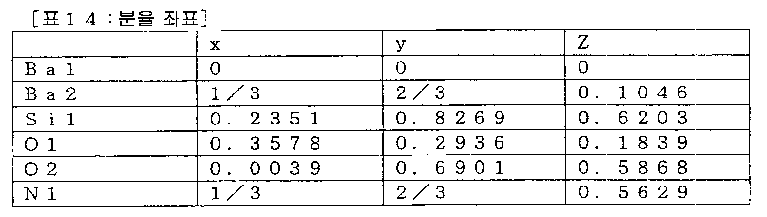
이와 같이, P3, P(3-) 와 상이한 공간군에 의해 분율 좌표를 구하였으나, 대상으로 한 알려지지 않은 물질이 갖는 결정 구조 중의 원자가 나타내는 공간 위치가 거의 바뀌는 경우는 없다.Thus, although fractional coordinates were calculated | required by the space group different from P3 and P (3-), the spatial position represented by the atom in the crystal structure of the unknown target object hardly changes.
이와 같이 결정한 단위 격자 내의 원자수를 확인하고, 당해 결정의 조성은, Ba3Si6O12N2:Eu 인 것이 판명되었다.The number of atoms in the unit lattice thus determined was confirmed, and the composition of the crystal was found to be Ba 3 Si 6 O 12 N 2 : Eu.
(실시예 70 ∼ 74)(Examples 70-74)
투입 조성이 표 15 에 나타내는 조성비가 되도록, BaCO3 을 5.78g, SiO2 를 3.34g, Si3N4 를 1.95g, Eu2O3 을 0.32g 사용하였다.5.78 g of BaCO 3 , 3.34 g of SiO 2 , 1.95 g of Si 3 N 4 , and 0.32 g of Eu 2 O 3 were used so that the charged composition was the composition ratio shown in Table 15.
실시예 70 및 71 에 있어서는, 이들 원료 분말을 마노 자동 막자사발에 모두 넣어 에탄올을 첨가하고, 습식 혼합법에 의해 균일해질 때까지 혼합하였다. 이렇게 하여 얻어진 페이스트상 혼합물을 건조 후, 알루미나 도가니에 각각 충전하고, 가볍게 하중을 가하여 충전물을 압축 성형하였다. 이것을 온도 조절기 장착 저항 가열식 관상 전기로 내에 두고, 대기압하에서, 0.5ℓ/min 의 질소 96 체적% + 수소 4 체적% 의 혼합 기류 중, 4.8℃/min 의 승온 속도로 1200℃ 까지 가열하고, 그 온도에서 4 시간 유지한 후, 실온까지 방랭시켰다. 얻어진 시료는 알루미늄 막자사발로 분쇄하고, 분쇄한 시료는 한번 더 알루미나 도가니에 각각 충전하고, 가볍게 하중을 가하여 충전물을 압축 성형하였다. 이 알루미나 도가니는 온도 조절기 장착 저항 가열식 관상 전기로 내에 놓여지고, 대기압하에서, 0.5ℓ/min 의 질소 96 체적% + 수소 4 체적% 의 혼합 기류 중, 4.8℃/min 의 승온 속도로 1300℃ 까지 가열되고, 그 온도에서 4 시간 유지하고, 그 후, 실온까지 방랭시켰다.In Examples 70 and 71, all of these raw powders were put in an agate automatic mortar and ethanol was added and mixed until uniform by a wet mixing method. The paste mixture thus obtained was dried and then filled in an alumina crucible, respectively, and lightly applied to the filling to compression molding. This was placed in a resistance heating tubular electric furnace equipped with a temperature controller, and heated to 1200 ° C. at a temperature rising rate of 4.8 ° C./min in a mixed air flow of 96% by volume of nitrogen and 4% by volume of hydrogen at 0.5 L / min under atmospheric pressure. After maintaining for 4 hours at room temperature, it was allowed to cool to room temperature. The obtained sample was ground with an aluminum mortar, and the ground samples were once again filled in an alumina crucible, lightly loaded, and the filling was compression molded. This alumina crucible is placed in a resistance heating tubular electric furnace equipped with a temperature controller, and is heated to 1300 ° C. at an elevated temperature rate of 4.8 ° C./min in a mixed airflow of 96% by volume of nitrogen and 4% by volume of hydrogen at 0.5 L / min under atmospheric pressure. The mixture was kept at that temperature for 4 hours, and then allowed to cool to room temperature.
실시예 72 에 있어서는, 상기 서술한 실시예 70 및 71 의 방법 중, 소성 온도 1300℃ 를 1400℃ 로 변경한 것 이외에는 동일하게 하여 실시하였다.In Example 72, it carried out similarly except having changed the baking temperature of 1300 degreeC into 1400 degreeC among the methods of Example 70 and 71 mentioned above.
실시예 73 에 있어서는, 이들 원료 분말을 마노 자동 막자사발에 모두 넣어 에탄올을 첨가하고, 습식 혼합법에 의해 균일해질 때까지 혼합하였다. 이렇게 하여 얻어진 페이스트상 혼합물을 건조 후, 질화붕소 도가니에 분말인 채로 충전하고, 이것에 가볍게 하중을 가하여 압축 성형하였다. 이 질화붕소 도가니를 먼저, 저항 가열식 전기로에 내에 설치하고, 대기 중에서, 실온으로부터 승온 속도 5℃/min 으로 1100℃ 까지 가열하고, 그 온도에서 3 시간 유지한 후, 실온까지 방랭시켰다. 그 후, 얻어진 예비 소성물을 알루미나 막자사발로 분쇄 혼합한 후, 질화붕소 도가니에 분말인 채로 충전하고, 이것에 가볍게 하중을 가하여 압축 성형하였다. 이 질화붕소 도가니를 저항 가열식 진공 가압 분위기 열처리로 (후지 전파 공업 제조) 에 내에 설치하고, < 5 × 10⁻³Pa 의 감압하에서, 실온부터 800℃ 까지 승온 속도 20℃/min 으로 진공 가열하였다. 800℃ 에 도달하였을 때, 그 온도에서 유지하여 압력이 0.92MPa 가 될 때까지 고순도 질소 가스 (99.9995%) 를 30 분간 도입하였다.In Example 73, all of these raw powders were put in an agate automatic mortar and ethanol was added, and mixed until wet by a wet mixing method. The paste-like mixture thus obtained was dried and then filled into a boron nitride crucible as a powder, which was lightly loaded and compression molded. This boron nitride crucible was first installed in a resistance heating electric furnace, heated from room temperature to 1100 ° C. at a temperature increase rate of 5 ° C./min, held at that temperature for 3 hours, and then allowed to cool to room temperature. Thereafter, the obtained pre-fired product was pulverized and mixed with an alumina mortar, and then filled into a boron nitride crucible as a powder, which was lightly loaded and compression molded. This boron nitride crucible was placed in a resistance heating vacuum pressurized atmosphere heat treatment furnace (manufactured by Fuji Propagation Industry Co., Ltd.), and was vacuum heated at room temperature to 800 ° C. under a reduced pressure of <5 × 10 −3 Pa at a temperature increase rate of 20 ° C./min. When it reached 800 degreeC, high-purity nitrogen gas (99.9995%) was introduce | transduced for 30 minutes, maintaining at that temperature and until a pressure became 0.92 Mpa.
도입 후, 0.92MPa 를 유지하면서, 다시 승온 속도 20℃/min 으로 1200℃ 까지 승온시켰다. 그 온도에서 5 분간 유지하여 열전대로부터 방사 온도계로 바꾸고, 다시 승온 속도 20℃/min 으로 1300℃ 까지 가열하였다. 1300℃ 에 도달하였을 때 2 시간 유지하고, 그 후 1200℃ 까지 강온 속도 20℃/min 으로 냉각시키고, 이어서 방랭시켰다. 얻어진 소성물을 다시 알루미늄 막자사발로 분쇄하고, 분쇄한 시료는 한번 더 알루미나 도가니에 각각 충전하고, 가볍게 하중을 가하여 충전물을 압축 성형하였다. 이 알루미나 도가니는 온도 조절기 장착 저항 가열식 관상 전기로 (실리코니트사 제조) 내에 놓여지고, 대기압하에서, 0.5ℓ/min 의 질소 기류 중, 4.8℃/min 의 승온 속도로 1300℃ 까지 가열되고, 그 온도에서 48 시간 유지하고, 그 후, 실온까지 방랭시켰다.It heated up to 1200 degreeC at the temperature increase rate of 20 degreeC / min again, maintaining 0.92 Mpa after introduction. It hold | maintained at that temperature for 5 minutes, it changed from the thermocouple to the radiation thermometer, and heated again to 1300 degreeC with the temperature increase rate of 20 degreeC / min. When it reached 1300 degreeC, it hold | maintained for 2 hours, Then, it cooled to 1200 degreeC, and cooled at 20 degree-C / min of temperature-fall rate, and then left to cool. The obtained fired material was again ground with an aluminum mortar, and the pulverized samples were once again filled in an alumina crucible, and lightly loaded to form a compact. This alumina crucible is placed in a resistance heating tubular electric furnace equipped with a temperature controller (manufactured by Silconite Co., Ltd.), and is heated to 1300 ° C. at an elevated temperature rate of 4.8 ° C./min in a nitrogen gas stream of 0.5 L / min under atmospheric pressure, and the temperature thereof. The mixture was kept for 48 hours, and then allowed to cool to room temperature.
얻어진 시료에 대해서는, N-NO355T (오프닝 37㎛) 나일론체에 의해 체 처리를 하였다.About the obtained sample, the sieve process was performed by the N-NO355T (opening 37 micrometers) nylon body.
또, 실시예 74 는 상기 실시예 73 에 있어서, 체 상에 잔류한 것을 시료로서 사용하였다.In Example 74, what was left on a sieve was used as a sample in Example 73.
여기서, 실시예 72 및 73 에 있어서는, 원료 Si3N4 로서 각각 이하의 처리를 실시하여 얻어진 β-Si3N4 를 사용하였다.Here, in Examples 72 and 73, β-Si 3 N 4 obtained by performing the following treatment was used as the raw material Si 3 N 4 , respectively.
α-Si3N4 (우베 흥산사 제조) 292g 을 질화붕소 도가니에 분말인 채로 충전하고, 가볍게 하중을 가하여 압축 성형하였다. 이 질화붕소 도가니를 저항 가열식 진공 가압 분위기 열처리로 (후지 전파 공업 제조) 에 내에 설치하고, < 5 × 10⁻³Pa 의 감압하에서, 실온부터 800℃ 까지 승온 속도 20℃/min 으로 진공 가열하였다. 800℃ 에 도달하였을 때, 그 온도에서 유지하여 압력이 0.92MPa 가 될 때까지 고순도 질소 가스 (99.9995%) 를 30 분간 도입하였다. 도입 후, 0.92MPa 를 유지하면서, 다시 승온 속도 20℃/min 으로 1200℃ 까지 승온시켰다. 그 온도에서 5 분간 유지하여 열전대로부터 방사 온도계로 바꾸고, 다시 승온 속도 20℃/min 으로 2000℃ 까지 가열하였다. 2000℃ 에 도달하였을 때 2 시간 유지하고, 다시 계속하여 20℃/min 으로 1800℃ 까지 가열하고, 그 온도에서 3 시간 유지하였다. 소성 후 1200℃ 까지 강온 속도 20℃/min 으로 냉각시키고, 이어서 방랭시켰다.292 g of α-Si 3 N 4 (manufactured by Ube Heungsan Co., Ltd.) was charged with a boron nitride crucible as a powder, and lightly loaded to compression molding. This boron nitride crucible was placed in a resistance heating vacuum pressurized atmosphere heat treatment furnace (manufactured by Fuji Propagation Industry Co., Ltd.), and was vacuum heated at room temperature to 800 ° C. under a reduced pressure of <5 × 10 −3 Pa at a temperature increase rate of 20 ° C./min. When it reached 800 degreeC, high-purity nitrogen gas (99.9995%) was introduce | transduced for 30 minutes, maintaining at that temperature and until a pressure became 0.92 Mpa. It heated up to 1200 degreeC at the temperature increase rate of 20 degreeC / min again, maintaining 0.92 Mpa after introduction. It hold | maintained at that temperature for 5 minutes, it changed from the thermocouple to the radiation thermometer, and heated again to 2000 degreeC at the temperature increase rate of 20 degreeC / min. When it reached 2000 degreeC, it hold | maintained for 2 hours, and it heated again at 20 degree-C / min to 1800 degreeC, and kept at that temperature for 3 hours. After baking, it cooled to the temperature-fall rate of 20 degree-C / min, and then cooled to 1200 degreeC.
상기 처리를 실시하기 전 및 실시한 후의 Si3N4 에 대해, X 선 회절 측정 및 반사 스펙트럼 측정을 실시하였다. 각각의 X 선 회절 패턴을 PDF (Powder Diffraction File) 76-1407 및 75-0950 에 있는 α-Si3N4 및 β-Si3N4 의 피크와 비교한 결과, 처리 전에는 α-Si3N4 였던 것이, 상기 처리에 의해 β-Si3N4 로 완전히 상전이되어 있는 것이 확인되었다.X-ray diffraction measurement and reflection spectrum measurement were performed about Si 3 N 4 before and after the treatment. Each X-ray diffraction pattern was compared with the peaks of α-Si 3 N 4 and β-Si 3 N 4 in Powder Diffraction Files (PDF) 76-1407 and 75-0950, and before treatment, α-Si 3 N 4 As a result, it was confirmed that the phase was completely phase shifted to β-Si 3 N 4 by the above treatment.
또, 상기α-Si3N4 및 β-Si3N4 의 반사 스펙트럼도를 도 36 에 나타낸다. 이 점에서, 상기 처리에 의해 얻어진 β-Si3N4 는 α-Si3N4 와 비교하여, 반사율이 높은 것을 알 수 있다.36 is a reflection spectral diagram of the α-Si 3 N 4 and β-Si 3 N 4 . From this point, it can be seen that β-Si 3 N 4 obtained by the above treatment has a higher reflectance than α-Si 3 N 4 .
또, 이들 α-Si3N4 와 β-Si3N4 에 대해 잔류 카본량을 고주파로 가열 연소 추출-비분산 적외 검출법 (호리바 제작소 제조, EMIA520FA 형) 으로 측정한 결과, α-Si3N4 에서는 0.1 중량%, β-Si3N4 에서는 0.02 중량% 이고, β-Si3N4 쪽이 적었다. 또한 이들의 SEM 관찰의 결과로부터, α-Si3N4 에서는 평균 입경이 0.2 ∼ 0.5㎛ 이었으나, β-Si3N4 는 평균 입경이 1 ∼ 2㎛ 이었다.In addition, these α-Si 3 N 4 and β-Si 3 N 4 extracts heat the residual carbon amount in the high-frequency combustion for - was measured with a non-dispersion infrared detection method (Horiba Manufacturing, EMIA520FA type), α-Si 3 N 4, the 0.1 wt%, β-Si 3 N 4, and 0.02% by weight, β-Si 3 N 4 side is low. From the results of these SEM observations, the average particle diameter was 0.2 to 0.5 µm in α-Si 3 N 4 , but the average particle diameter of β-Si 3 N 4 was 1 to 2 µm.
상기 실시예 70 ∼ 74 에 있어서 얻어진 소성물의 X 선 회절 패턴을 도 37 에 나타낸다. 이 결과로부터, BSON 상이 주상으로 확인되었다. 또 이들의 소성물에 대해 형광 특성을 평가한 결과를 표 15 에 나타내고, 파장 400㎚ 여기 및 파장 455㎚ 여기에서의 발광 스펙트럼도를 각각 도 38 및 도 39 에 나타낸다. 발광 특성은 소성 시간을 비롯하여, 합성 방법 (유리상 상 (相) 을 재소성 조작을 실시하는 등) 을 바꿈으로써 발광 특성을 개선할 수 있었다.37 shows the X-ray diffraction patterns of the fired products obtained in Examples 70 to 74. FIG. From this result, the BSON phase was confirmed as a main phase. Moreover, the result of having evaluated the fluorescence characteristic about these baking products is shown in Table 15, and the luminescence spectrum diagram in wavelength 400nm excitation and wavelength 455nm excitation is shown in FIG. 38 and FIG. 39, respectively. The luminescence properties were able to improve the luminescence properties by changing the synthesis method (such as recalcining the glass phase) as well as the firing time.

또, 이들의 소성물에 대해, 추가로 발광 효율, 흡수 효율 및 내부 양자 효율을 구하였다. 결과를 표 16 에 나타낸다.Moreover, the luminous efficiency, absorption efficiency, and internal quantum efficiency were calculated | required further about these baking products. The results are shown in Table 16.

발광 효율은, 모두 20% 이상이고, 출발 원료의 Si3N4 를 α 체 (실시예 71) 로부터 β 체 (실시예 72) 로 바꾸면 30% 이상으로 증대하였다. 또, 소성 시간을 비롯하여, 합성 방법 (유리상 상을 재소성 조작을 실시하는 등) 을 바꿈으로써, 40% 이상으로까지 개선할 수 있었다.The luminous efficiency was 20% or more in all, and increased to 30% or more when the Si 3 N 4 of the starting material was changed from the α body (Example 71) to the β body (Example 72). Moreover, it was able to improve to 40% or more by changing the synthesis method (such as recalcining a glassy phase) including baking time.
한편, 흡수 효율은 모두 40% 이상이고, 마찬가지로 소성 시간을 비롯한 합성 조건을 바꿈으로써 60% 이상으로까지 향상시킬 수 있고, 또한, N-NO355T (오프닝 37㎛) 나일론에 의해 체질 조작을 하였을 때의 체 상에 남은 시료인 실시예 74 에서는 70% 이상의 값을 얻을 수 있었다.On the other hand, the absorption efficiency is all 40% or more, and can be improved to 60% or more by changing the synthetic conditions including the firing time, and also when sieving operation is performed by N-NO355T (opening 37 µm) nylon. In Example 74, which was the sample remaining on the sieve, a value of 70% or more was obtained.
또, 내부 양자 효율은 발광 효율을 흡수 효율로 나눈 값이다.The internal quantum efficiency is a value obtained by dividing the luminous efficiency by the absorption efficiency.
(실시예 75 및 76)(Examples 75 and 76)
투입 조성이 표 17 에 나타내는 조성비가 되도록, BaCO3 을 6.02g, SiO2 를 2.87g, Si3N4 를 2.23g, Eu2O3 을 0.34g 사용하였다.In the composition so that the composition ratio shown in Table 17, 2.87g of the BaCO 3 6.02g, SiO 2, Si 3
이들 원료 분말을 마노 자동 막자사발에 모두 넣어 에탄올을 첨가하고, 습식 혼합법에 의해 균일해질 때까지 혼합하였다. 이렇게 하여 얻어진 페이스트상 혼합물을 건조 후, 알루미나 도가니에 각각 충전하고, 가볍게 하중을 가하여 충전물을 압축 성형하였다. 이것을 온도 조절기 장착 저항 가열식 관상 전기로 내에 두고, 대기압하에서, 0.5ℓ/min 의 질소 96 체적% + 수소 4 체적% 의 혼합 기류 중, 4.8℃/min 의 승온 속도로 1200℃ 까지 가열하고, 그 온도에서 4 시간 유지한 후, 실온까지 방랭시켰다. 얻어진 시료는 알루미늄 막자사발로 분쇄하고, 분쇄한 시료는 한번 더 알루미나 도가니에 각각 충전하고, 가볍게 하중을 가하여 충전물을 압축 성형하였다. 이 알루미나 도가니는 온도 조절기 장착 저항 가열식 관상 전기로 내에 놓여지고, 대기압하에서, 0.5ℓ/min 의 질소 96 체적% + 수소 4 체적% 의 혼합 기류 중, 4.8℃/min 의 승온 속도로 1350℃ 까지 가열되고, 그 온도에서 72 시간 유지하고, 그 후, 실온까지 방랭시켰다.These raw material powders were all put in agate automatic mortar, ethanol was added, and mixed until it became uniform by the wet mixing method. The paste mixture thus obtained was dried and then filled in an alumina crucible, respectively, and lightly applied to the filling to compression molding. This was placed in a resistance heating tubular electric furnace equipped with a temperature controller, and heated to 1200 ° C. at a temperature rising rate of 4.8 ° C./min in a mixed air flow of 96% by volume of nitrogen and 4% by volume of hydrogen at 0.5 L / min under atmospheric pressure. After maintaining for 4 hours at room temperature, it was allowed to cool to room temperature. The obtained sample was ground with an aluminum mortar, and the ground samples were once again filled in an alumina crucible, lightly loaded, and the filling was compression molded. This alumina crucible is placed in a resistance heating tubular electric furnace equipped with a temperature controller, and is heated to 1350 ° C. at an elevated temperature rate of 4.8 ° C./min in a mixed air flow of 96% by volume of nitrogen and 4% by volume of hydrogen at 0.5 L / min under atmospheric pressure. The mixture was kept at that temperature for 72 hours, and then allowed to cool to room temperature.
여기서, 상기 실시예 76 에 있어서는, Si3N4 로서 상기 서술한 처리를 실시한 β-Si3N4 를 사용하였다.Here, in the above Example 76, it was used as β-Si 3 N 4 Si 3 N 4 subjected to the aforementioned treatment.
상기 실시예 75 및 76 에서 얻어진 소성물은, 실시예 75 에서 얻어진 합성 분체보다 실시예 76 에서 얻어진 분체 쪽이, 체색이 선명한 녹색이었다. 또, 그 X 선 회절 패턴을 도 40 에 나타낸다. 이 결과로부터, 모두 BSON 상이 주상으로 확인되었다. 또 이들의 소성물에 대해 형광 특성을 평가한 결과를 표 17 에 나타내고, 파장 400㎚ 여기 및 파장 455㎚ 여기에서의 발광 스펙트럼도를 각각 도 41 및 도 42 에 나타낸다.In the fired products obtained in Examples 75 and 76, the powder obtained in Example 76 was greener in color than the synthetic powder obtained in Example 75. Moreover, the X-ray diffraction pattern is shown in FIG. From this result, the BSON phase was confirmed as the main phase in all. Moreover, the result of having evaluated the fluorescence characteristic about these baking products is shown in Table 17, and the emission spectral diagram in wavelength 400nm excitation and wavelength 455nm excitation is shown in FIG. 41 and FIG. 42, respectively.
얻어진 발광의 피크 위치는 거의 변화가 없었으나, 실시예 76 쪽이 발광 피크가 높았다.The peak position of the obtained light emission was almost unchanged, but Example 76 had a high light emission peak.
또한, 실시예 76 에서 얻어진 소성물의 여기 스펙트럼도를 도 43 에 나타낸다.43 shows the excitation spectral diagram of the fired product obtained in Example 76. FIG.

(실시예 77)(Example 77)
투입의 조성비가 Ba3Si6O12N2 가 되도록, BaCO3 을 15.1g, SiO2 를 6.76g, Si3N4 를 1.75g 사용하였다.15.1 g of BaCO 3 , 6.76 g of SiO 2 , and 1.75 g of Si 3 N 4 were used so that the composition ratio of the charge was Ba 3 Si 6 O 12 N 2 .
이들 원료 분말을 마노 자동 막자사발에 모두 넣어 에탄올을 첨가하고, 습식 혼합법에 의해 균일해질 때까지 혼합하였다. 이렇게 하여 얻어진 페이스트상 혼합물을 건조 후, 알루미나 도가니에 각각 충전하고, 가볍게 하중을 가하여 충전물을 압축 성형하였다. 이것을 온도 조절기 장착 저항 가열식 관상 전기로 내에 두고, 대기압하에서, 0.5ℓ/min 의 질소 96 체적% + 수소 4 체적% 의 혼합 기류 중, 4.8℃/min 의 승온 속도로 1200℃ 까지 가열하고, 그 온도에서 4 시간 유지한 후, 실온까지 방랭시켰다. 얻어진 시료는 알루미늄 막자사발로 분쇄하고, 분쇄한 시료는 한번 더 알루미나 도가니에 각각 충전하고, 가볍게 하중을 가하여 충전물을 압축 성형하였다. 이 알루미나 도가니는 온도 조절기 장착 저항 가열식 관상 전기로 내에 놓여지고, 대기압하에서, 0.5ℓ/min 의 질소 기류 중, 4.8℃/min 의 승온 속도로 1350℃ 까지 가열되고, 그 온도에서 10 시간 유지하고, 그 후, 실온까지 방랭시켰다. 얻어진 소성물을 다시 알루미늄 막자사발로 분쇄하고, 분쇄한 시료는 한번 더 알루미나 도가니에 각각 충전하고, 가볍게 하중을 가하여 충전물을 압축 성형하였다. 이 알루미나 도가니는 온도 조절기 장착 저항 가열식 관상 전기로 내에 놓여지고, 대기압하에서, 0.5ℓ/min 의 질소 96 체적% + 수소 4 체적% 의 혼합 기류 중, 4.8℃/min 의 승온 속도로 1400℃ 까지 가열되고, 그 온도에서 4 시간 유지하고, 그 후, 실온까지 방랭시켰다.These raw material powders were all put in agate automatic mortar, ethanol was added, and mixed until it became uniform by the wet mixing method. The paste mixture thus obtained was dried and then filled in an alumina crucible, respectively, and lightly applied to the filling to compression molding. This was placed in a resistance heating tubular electric furnace equipped with a temperature controller, and heated to 1200 ° C. at a temperature rising rate of 4.8 ° C./min in a mixed air flow of 96% by volume of nitrogen and 4% by volume of hydrogen at 0.5 L / min under atmospheric pressure. After maintaining for 4 hours at room temperature, it was allowed to cool to room temperature. The obtained sample was ground with an aluminum mortar, and the ground samples were once again filled in an alumina crucible, lightly loaded, and the filling was compression molded. This alumina crucible is placed in a resistance heating tubular electric furnace equipped with a temperature controller, and is heated to 1350 ° C. at an elevated temperature rate of 4.8 ° C./min in a nitrogen stream of 0.5 L / min under atmospheric pressure, and maintained at that temperature for 10 hours. Thereafter, it was allowed to cool to room temperature. The obtained fired material was again ground with an aluminum mortar, and the pulverized samples were once again filled in an alumina crucible, and lightly loaded to form a compact. This alumina crucible is placed in a resistance heating tubular electric furnace equipped with a temperature controller, and is heated to 1400 ° C. at an elevated temperature rate of 4.8 ° C./min in a mixed airflow of 96% by volume of nitrogen and 4% by volume of hydrogen at 0.5 L / min under atmospheric pressure. The mixture was kept at that temperature for 4 hours, and then allowed to cool to room temperature.
얻어진 소성물의 X 선 회절 패턴을 도 44 에 나타낸다. 이 결과로부터, BSON 상이 주상으로 확인되었다.The X-ray diffraction pattern of the obtained fired product is shown in FIG. 44. From this result, the BSON phase was confirmed as a main phase.
(실시예 78 ∼ 87)(Examples 78 to 87)
투입 조성이 표 18 에 나타내는 조성비가 되도록, BaCO3, SiO2, Si3N4, MnO2 (쥰세이 화학사 제조), Pr6O11 (후루우치 화학사 제조), Nd2O3 (닛산 희원소 화학사 제조), Sm2O3 (미츠와 화학 약품사 제조), Tb4O7 (신에츠 화학 (주) 사 제조), Dy2O3 (닉키사 제조), Ho2O3 (후루우치 화학사 제조), Er2O3 (닛산 희원소 화학사 제조), Tm2O3 (신에츠 화학 (주) 사 제조), Yb2O3 (후루우치 화학사 제조) 을 각각 칭량하였다. 즉, 실시예 78 에 있어서는, BaCO3 을 5.82g, SiO2 를 3.50g, Si3N4 를 2.05g, MnO2 를 0.03g 사용하고, 실시예 79 에 있어서는, BaCO3 을 5.80g, SiO2 를 3.50g, Si3N4 를 2.04g, Pr6O11 을 0.05g 사용하였다. 이 밖의 실시예는, 각 조성비에 따라, 상기 투입량을 기준으로 그 배합량을 결정하였다.BaCO 3 , SiO 2 , Si 3 N 4 , MnO 2 (manufactured by Junsei Chemical Co., Ltd.), Pr 6 O 11 (manufactured by Furuchi Chemical Co., Ltd.), Nd 2 O 3 (manufactured by Nissan Rare Element Chemical Co., Ltd.) ), Sm 2 O 3 (manufactured by Mitsuwa Chemicals, Inc.), Tb 4 O 7 (manufactured by Shin-Etsu Chemical Co., Ltd.), Dy 2 O 3 (manufactured by Nikki Corporation), Ho 2 O 3 (manufactured by Furuchi Chemical Co., Ltd.), Er 2 O 3 (manufactured by Nissan Rare Element Chemical Co., Ltd.), Tm 2 O 3 (manufactured by Shin-Etsu Chemical Co., Ltd.), and Yb 2 O 3 (manufactured by Furuchi Chemical Co., Ltd.) were weighed respectively. That is, in Example 78, 5.82 g of BaCO 3 , 3.50 g of SiO 2 , 2.05 g of Si 3 N 4 , and 0.03 g of MnO 2 were used. In Example 79, 5.80 g of BaCO 3 and SiO 2 were used. 3.50 g, 2.04 g Si 3 N 4 and 0.05 g Pr 6 O 11 were used. In the other examples, the compounding amount was determined based on the above-mentioned amount according to each composition ratio.
이들 원료 분말을 마노 자동 막자사발에 모두 넣어 에탄올을 첨가하고, 습식 혼합법에 의해 균일해질 때까지 혼합하였다. 이렇게 하여 얻어진 페이스트상 혼합물을 건조 후, 알루미나 도가니에 각각 충전하고, 가볍게 하중을 가하여 충전물을 압축 성형하였다. 이것을 온도 조절기 장착 저항 가열식 관상 전기로 내에 두고, 대기압하에서, 0.5ℓ/min 의 질소 96 체적% + 수소 4 체적% 의 혼합 기류 중, 4.8℃/min 의 승온 속도로 1200℃ 까지 가열하고, 그 온도에서 4 시간 유지한 후, 실온까지 방랭시켰다. 얻어진 시료는 알루미늄 막자사발로 분쇄하고, 분쇄한 시료는 한번 더 알루미나 도가니에 각각 충전하고, 가볍게 하중을 가하여 충전물을 압축 성형하였다. 이 알루미나 도가니는 온도 조절기 장착 저항 가열식 관상 전기로 내에 놓여지고, 대기압하에서, 0.5ℓ/min 의 질소 기류 중, 4.8℃/min 의 승온 속도로 1300℃ 까지 가열되고, 그 온도에서 10 시간 유지하고, 그 후, 실온까지 방랭시켰다.These raw material powders were all put in agate automatic mortar, ethanol was added, and mixed until it became uniform by the wet mixing method. The paste mixture thus obtained was dried and then filled in an alumina crucible, respectively, and lightly applied to the filling to compression molding. This was placed in a resistance heating tubular electric furnace equipped with a temperature controller, and heated to 1200 ° C. at a temperature rising rate of 4.8 ° C./min in a mixed air flow of 96% by volume of nitrogen and 4% by volume of hydrogen at 0.5 L / min under atmospheric pressure. After maintaining for 4 hours at room temperature, it was allowed to cool to room temperature. The obtained sample was ground with an aluminum mortar, and the ground samples were once again filled in an alumina crucible, lightly loaded, and the filling was compression molded. This alumina crucible is placed in a resistance heating tubular electric furnace equipped with a temperature controller, and is heated to 1300 ° C. at a temperature rising rate of 4.8 ° C./min in a nitrogen stream of 0.5 L / min under atmospheric pressure, and maintained at that temperature for 10 hours. Thereafter, it was allowed to cool to room temperature.
얻어진 소성물의 X 선 회절 패턴을 도 45 에 나타낸다. 이 결과로부터, 모든 실시예에서 BSON 상이 주상으로서 검출되었다.45 shows the X-ray diffraction pattern of the obtained fired product. From this result, the BSON phase was detected as a main phase in all the Examples.

[3. 발광 장치][3. Light emitting device]
[3-1. 청색 발광 다이오드를 사용한 발광 장치의 제조와 평가][3-1. Fabrication and Evaluation of Light-Emitting Device Using Blue Light-Emitting Diode]
이하에 나타내는 발광 장치의 제조에 사용한 각 형광체의 제조 방법을 참고예로서 기재한다.The manufacturing method of each fluorescent substance used for manufacture of the light emitting device shown below is described as a reference example.
(참고예 1:CaAlSiN3:Eu 의 제조)(Reference Example 1: CaAlSiN 3 : Manufacture of Eu)
제조되는 형광체의 화학 조성비가 Ca0 .992AlEu0 .008SiN3 이 되도록, 형광체 1 몰에 대한 비로, Ca3N2 를 0.331 몰, AlN 을 1 몰, Si3N4 를 0.363 몰, Eu2O3 을 0.004 몰이 되도록 각 원료 분말을 칭량하였다. 그것들을 탁상 믹서로 혼합하고, 질화붕소 도가니 중에서, 0.5MPa 의 질소 분위기 중, 최고 1800℃ 에서 2 시간 소성하였다. 얻어진 소성분을, 알루미나 막자사발 상에서 분쇄하고, 450㎛ 와 224㎛ 의 나일론 메시에 통과시켰다. 그 후 순수 중에서 1 시간 교반하고, 볼 밀 분쇄 처리를 실시하였다. 계속하여, 입경을 정렬하기 위한 분급 처리, 건조를 실시함으로써 Ca0 .992AlEu0 .008SiN3 을 제조하였다.The chemical composition ratio of the phosphor produced Ca 0 .992 0 .008 AlEu SiN 3 ratio for the phosphor to be 1 mol, the Ca 3 N 2 0.331 mol, 1 mol of AlN, 0.363 mole of Si 3 N 4, Eu 2 Each raw material powder was weighed so that O 3 became 0.004 mol. They were mixed by the tabletop mixer, and it baked in the boron nitride crucible at the maximum 1800 degreeC in 0.5 MPa nitrogen atmosphere for 2 hours. The obtained minor component was ground on an alumina mortar and passed through a 450 micrometer and 224 micrometer nylon mesh. Then, it stirred in pure water for 1 hour and performed the ball mill grinding process. Then, the classification process to sort the particle size, by carrying out drying to prepare a Ca 0 .992 0 .008 AlEu SiN 3.
(참고예 2:Sr2Si5N8:Eu 의 제조)(Reference Example 2: Sr 2 Si 5 N 8 : Production of Eu)
제조되는 형광체의 화학 조성비가 Sr1 .96Eu0 .04Si5N8 이 되도록, 형광체 1 몰에 대한 비로, SrCO3 을 1.96 몰, Si3N4 를 1.666 몰, Eu2O3 을 0.02 몰이 되도록 각 원료 분말을 칭량하였다. 그것들을 마노 막자사발 상에서 습식 혼합하고, 카본 도가니 중에서, 0.92MPa 의 질소 분위기 중, 최고 1800℃ 에서 2 시간 소성하였다. 얻어진 소성분을, 마노 막자사발을 사용하여 분쇄하고, 질화붕소 도가니 중에서, 0.92MPa 의 질소 분위기 중, 최고 1800℃ 에서 2 시간 소성하였다. 소성분을 분쇄하여 37㎛ 의 나일론 메시를 통과시켰다.The chemical composition ratio of the phosphor to be produced such that the Sr 1 .96 Eu 0 .04 Si 5
(참고예 3:Sr0 .8Ca0 .2AlSiN3:Eu 의 제조)(Reference Example 3: Sr 0 .8 Ca 0 .2 AlSiN 3: Preparation of Eu)
〈모합금의 제조〉<Production of master alloy>
금속 원소 조성비가 Al:Si = 1:1 (몰비) 이 되도록 각 금속을 칭량하고, 흑연 도가니를 사용하고, 아르곤 분위기에서 고주파 유도식 용융로를 사용하여 원료 금속을 용융한 후, 도가니로부터 금형으로 주탕 (注湯) 하여 응고시키고, 금속 원소 조성 원소비가 Al:Si = 1:1 인 합금을 얻었다.Each metal is weighed so that the metal element composition ratio is Al: Si = 1: 1 (molar ratio), a graphite crucible is used, and a raw metal is melted in an argon atmosphere using a high frequency induction melting furnace, followed by pouring from a crucible into a mold. (V) and solidified to obtain an alloy in which the metal element composition element ratio was Al: Si = 1: 1.
〈형광체 원료용 합금의 제조〉<Production of alloy for phosphor raw material>
Eu:Sr:Ca:Al:Si = 0.008:0.792:0.2:1:1 (몰비) 이 되도록 모합금, 그 외 원료 금속을 칭량하였다. 노 내를 5 × 10⁻²Pa 까지 진공 배기한 후, 배기를 중지시키고, 노 내에 아르곤을 소정압까지 충전하였다. 이 노 내에서, 칼시아 도가니 내에서 모합금을 용해시키고, 이어서 Sr 을 용해시키고, 도가니로부터 용탕을 금형으로 주탕하여 응고시켰다.The master alloy and other raw metals were weighed so that Eu: Sr: Ca: Al: Si = 0.008: 0.792: 0.2: 1: 1 (molar ratio). After evacuating the inside of the furnace to 5 × 10 −2 Pa, the exhaust was stopped and argon was charged to a predetermined pressure in the furnace. In this furnace, the master alloy was dissolved in a Calcia crucible, then Sr was dissolved, and the molten metal was poured into a mold from the crucible and solidified.
얻어진 합금을 질소 분위기하에서 알루미나 막자사발을 사용하여 조 (粗) 분쇄한 것을, 초음속 제트 분쇄기를 사용하여 질소 분위기하에서, 분쇄 압력 0.15MPa, 원료 공급 속도 0.8㎏/hr 로 분쇄하였다. 얻어진 합금 분말을, 물 세정, 분급 처리, 건조를 실시함으로써 Sr0 .792Ca0 .200AlEu0 .008SiN3 을 제조하였다.The obtained alloy was pulverized by using an alumina mortar in a nitrogen atmosphere, and then pulverized at a grinding pressure of 0.15 MPa and a raw material feed rate of 0.8 kg / hr in a nitrogen atmosphere using a supersonic jet grinder. The resulting alloy powder was prepared by Sr 0 .792 Ca 0 .200 AlEu 0 .008
(참고예 4:Sr2BaSiO5:Eu 의 제조)(Reference Example 4: Production of Sr 2 BaSiO 5 : Eu)
조성식 BaSr1 .98Eu0 .02SiO5 가 되도록, 형광체 1 몰에 대한 비로, BaCO3 을 1 몰, SrCO3 을 1.98 몰, SiO2 를 1 몰, Eu2O3 을 0.02 몰이 되도록 각 원료 분말을 칭량하였다. 그것들을 마노 막자사발 상에서 습식 혼합하고, 몰리브덴박 중에서, 질소 분위기 중, 최고 1550℃ 에서 2 시간 소성하였다. 얻어진 소성분을, 알루미나 막자사발 상에서 분쇄하고, 플라티나박 중에서, 수소를 4 체적% 포함한 질소 분위기 중에서, 최고 1550℃ 에서 2 시간 소성하였다. 소성분을 분쇄하여 37㎛ 의 나일론 메시를 통과시켰다.Formula BaSr 1 .98 Eu 0 .02 SiO 5 is such that, the ratio of the
(참고예 5:(Ca,Sr)S:Eu 의 제조)(Reference Example 5: (Ca, Sr) S: Production of Eu)
제조되는 형광체의 화학 조성비가 Ca0 .5976Eu0 .004Sr0 .3984S 가 되도록, 형광체 1 몰에 대한 비로, CaS 를 0.5976 몰, SrS 를 0.3984 몰, EuF3 을 0.004 몰이 되도록 각 원료 분말을 칭량하였다. 그것들을 마노 막자사발 상에서 습식 혼합하고, 알루미나 도가니 중에서, 수소를 4 체적% 포함한 질소 분위기 중, 최고 1000℃ 에서 2 시간 소성하였다. 얻어진 소성분을 분쇄하여 37㎛ 의 나일론 메시를 통과시켰다.Each raw material powder the chemical composition ratio of the phosphor to be produced so that the Ca 0 .5976 Eu 0 .004 Sr 0 .3984 S is, the ratio, 0.5976 mol, 0.004 mol to 0.3984 mol, EuF 3 for the SrS phosphor CaS about 1 mole to Weighed. They were wet-mixed on an agate mortar and baked in alumina crucible at maximum 1000 degreeC for 2 hours in nitrogen atmosphere containing 4 volume% of hydrogen. The obtained small component was ground and passed through a 37 micrometer nylon mesh.
(참고예 6:Si5Al(O,N)8:Eu 의 제조)(Reference Example 6: Si 5 Al (O, N) 8 : Production of Eu)
제조되는 형광체의 화학 조성비가 Si5 .0029Al0 .9970Eu0 .0120O0 .0184N7 .9816 이 되도록, 형광체 1 몰에 대한 비로, AlN 을 0.333 몰, Al2O3 을 0.333 몰, Si3N4 를 1.666 몰, Eu2O3 을 0.006 몰, CaCO3 을 8.93 × 10⁻⁴ 몰이 되도록 각 원료 분말을 칭량하였다. 마노 막자사발 상에서 분쇄, 혼합하여 얻어진 혼합물을 질화붕소제의 도가니 중에서 0.92MPa 의 질소 분위기 중에서, 최고 1700℃ 에서 2 시간 소성하였다. 얻어진 소성분을, 막자사발을 사용하여 분쇄하고, 다시 질화붕소제의 도가니 중에서 0.92MPa 의 질소 분위기 중에서, 최고 2000℃ 에서 2 시간 소성하였다. 소성 후, 막자사발을 사용하여 분쇄하고, 37㎛ 의 나일론 메시를 통과시킴으로써 Si5.0029Al0.9970Eu0.0120O0.0184N7.9816 을 제조하였다.The chemical composition ratio of the phosphor produced Si 5 .0029 Al 0 .9970 Eu 0 .0120
(참고예 7:(Ba,Sr)2SiO4:Eu 의 제조)(Reference Example 7: (Ba, Sr) 2 SiO 4 : Production of Eu)
제조되는 형광체의 화학 조성비가 Ba1 .39Sr0 .46Eu0 .15SiO4 가 되도록, 형광체 1 몰에 대한 비로, BaCO3 을 1.39 몰, SrCO3 을 0.46 몰, Eu2O3 을 0.15 몰, SiO2 를 1 몰이 되도록 각 원료 분말을 칭량하였다. 그것들을 폴리백 중에서 건식 혼합하고, 100 미크론의 나일론 메시에 통과시켰다. 그 후 다시 폴리백 중에서 건식 혼합을 실시하였다. 얻어진 혼합물을 알루미나 도가니 중에 가볍게 중점하여 막자로 중앙에 구멍을 뚫었다. 알루미나제 도가니의 덮개를, 간극을 두고 도가니 위에 두었다. 생분 (生粉) 이 들어간 도가니를 질소 분위기 중의 환원 분위기로에서, 최고 1000℃ 에서 12 시간 소성하였다. 얻어진 소성분을 알루미나 막자사발 상에서 분쇄하고, 100㎛ 의 나일론 메시에 통과시킨 후, 플럭스로서 SrCl2·2H2O 를 생분 중량에 대해 12 중량% 혼입하고, 65㎛ 의 나일론 메시에 통과시켰다. 그것들을 알루미나 도가니 중에 가볍게 충전시켜 고체 카본 존재하의 CO 가스 함유 질소 분위기 중, 최고 온도 1190℃ 에서 5 시간 가열함으로써 소성하였다. 소성분을, 스탬프 밀을 사용하여 분쇄하고, 37㎛ 의 나일론 메시를 통과시켰다. 그것들에 5 배의 순수를 첨가하여 교반한 슬러리를 데칸테이션으로 농축시킨 후, 힘을 가하지 않고 37㎛ 의 나일론 메시로 물체질을 실시하였다. 그 후, 체 하를 일정량으로 희석시키고, 상청액의 미세 입자를 컷한다. 그 후 물 세정을 반복하여 용액의 전도율이 2mS/m 이하가 되도록 하고, 누체를 사용하여 탈수하고, 건조기 중에서, 150℃ 에서 10 시간 건조시켰다. 마무리로서 37㎛ 의 나일론 메시에 통과시킴으로써 Ba1 .39Sr0 .46Eu0 .15SiO4 를 제조하였다.The chemical composition ratio of the phosphor to be produced for the ratio, one mole of the phosphor so that the Ba 1 .39 Sr 0 .46 Eu 0 .15
(참고예 8:SrGa2S4:Eu 의 제조)(Reference Example 8: Production of SrGa 2 S 4 : Eu)
제조되는 형광체의 화학 조성비가 Sr0 .85Ga2Eu0 .15S4 가 되도록, 형광체 1 몰에 대한 비로, SrS 를 0.85 몰, Ga2S3 을 1 몰, EuF3 을 0.15 몰로 바꾼 것 이외에는 일본 공개특허공보 2003-291608호의 실시예 1 과 동일하게 하여 제조하였다. 즉, 제조되는 형광체의 화학 조성비가 Sr0 .85Ga2Eu0 .15S4 가 되도록, 형광체 1 몰에 대한 비로, SrS 를 0.85 몰, Ga2S3 을 1 몰, EuF3 을 0.15 몰이 되도록 각 원료 분말을 칭량하였다. 마노 막자사발 상에서 분쇄, 혼합하여 얻어진 혼합물을 알루미나제 도가니 중에서 아르곤 가스 유하, 최고 1000℃ 에서 8 시간 소성하였다. 얻어진 소성분을 알루미나 막자사발 상에서 분쇄하고, 입경을 제어함으로써 제조하였다.The chemical composition ratio of the phosphor to be produced such that the Sr 0 .85 Ga 2 Eu 0 .15
(참고예 9:SrSi2O2N2:Eu 의 제조)(Reference Example 9: SrSi 2 O 2 N 2 : Production of Eu)
1 차 소성에서 얻어지는 화합물의 화학 조성비가 Sr1 .92Eu0 .08Si1O4 가 되도록, 형광체 2 몰에 대한 비로, SrCO3 을 1.92 몰, SiO2 를 1 몰, Eu2O3 을 0.04 몰이 되도록 각 원료 분말을 칭량하였다. 알루미나 막자사발 상에서 분쇄, 혼합하여 얻어진 혼합물을 질화붕소제의 도가니 중에서 수소를 4 체적% 포함한 질소 분위기 중에서, 1250℃ 에서 3 시간 소성하였다. 다시 얻어진 소성물을 알루미나 막자사발 상에서 분쇄하여, 제조되는 형광체의 화학 조성비가 Sr0 .96Eu0 .04Si2O2N2 가 되도록, 형광체 2 몰에 대한 비로, Si3N4 를 1 몰 혼합하였다. 0.92MPa 의 질소 분위기 중에서, 최고 1450℃ 에서 2 시간 소성하였다. 얻어진 소성분을, 알루미나 막자사발 상에서 분쇄하여, 37㎛ 의 나일론 메시를 통과시킴으로써 Sr0.96Eu0.04Si2O2N2 를 제조하였다.First the chemical composition ratio of the obtained compound at a ratio of the plastic, so that the
(참고예 10:CaSc2O4:Ce 의 제조)(Reference Example 10: CaSc 2 O 4 : Production of Ce)
제조되는 형광체의 화학 조성비가 Ce0 .0065Ca0 .9935Sc2O4 가 되도록, 형광체 1 몰에 대한 비로, CaCO3 을 1.04 몰, Sc-Ce 공침품, Sc1 .9935Ce0 .0065O3 을 1 몰이 되도록 각 원료 분말을 칭량하였다. 그것들을 백 중에서 혼합하고, 224㎛ 의 나일론 메시에 통과시켰다. 얻어진 혼합물을 알루미나 도가니 중에서, 대기 분위기 중, 최고 1100 ∼ 1150℃ 에서 4 시간 소성하였다. 얻어진 소성분을, 막자사발을 사용하여 분쇄하고, 플럭스로서 CaCl2, Li3PO4, KCl 을 생분 중량에 대해 각각 10 중량%, 5 중량%, 1.5 중량% 혼입하고, 그것들을 백 중에서 혼합하여 100㎛ 의 나일론 메시에 통과시켰다. 그것들을 알루미나 도가니 중에서, 수소를 4 체적% 포함한 질소 분위기 중, 최고 온도 1450℃ 에서 9 시간 가열함으로써 소성하였다. 소성분이 식고 나서 알루미나 막자사발 상에서 분쇄를 하고, 0.6 리터의 용기 중에 3㎜ 의 알루미나 볼을 600g, 희염산과 분쇄한 가루를 넣어 회전 속도 60rpm 으로 4 시간 볼 밀 분쇄를 실시하였다. 볼 밀 종료 후, 순수로 희염산을 묽게 한 후, 65㎛ 의 나일론 메시에 습식으로 통과시켰다. 그 후 1N-HCl 로 분체를 세정하고, 분급 처리를 실시하여 약 5㎛ 이하의 입자를 컷하였다. 다시 얻어진 형광체를 100g 포함하는 500㎖ 의 용액 중에서, 소성분이 풀릴 때까지 교반하고, Na3PO4·12H2O 를 1.5㎖ 주입하여 교반하였다. 추가로 Ca(NO3)2·H2O 를 0.75㎖ 주입함으로써 코트 처리를 실시하였다. 이어서 대입자 컷을 하기 위해 40㎛ 와 25㎛ 의 나일론 메시를 통과시켰다. 그 후 물 세정을 반복하여 용액의 전도율이 2mS/m 이하가 되도록 하고, 누체를 사용하여 탈수하고, 건조기 중에서 150℃, 10 시간 건조시킴으로써 Ce0 .0065Ca0 .9935Sc2O4 를 제조하였다.The chemical composition ratio of the phosphor produced Ce 0 .0065 Ca 0 .9935 Sc 2 O ratio of the fluorescent material so that one mole of the 4, CaCO 3 of 1.04 mol, Sc-Ce ball chimpum, Sc 1 .9935 0 .0065 Ce O Each raw material powder was weighed so that 3 was 1 mol. They were mixed in a bag and passed through a 224 μm nylon mesh. The obtained mixture was baked in an alumina crucible at maximum 1100-1150 degreeC in air | atmosphere for 4 hours. The obtained minor components were ground using a mortar and pestle, and CaCl 2 , Li 3 PO 4 and KCl were mixed as flux with 10% by weight, 5% by weight and 1.5% by weight, respectively, and mixed in a bag. It passed through a 100 micrometer nylon mesh. They were baked in an alumina crucible by heating for 9 hours at a maximum temperature of 1450 ° C. in a nitrogen atmosphere containing 4% by volume of hydrogen. After a small component cooled, it grind | pulverized on the alumina mortar, 600 g of 3 mm alumina balls and the powder which grind | pulverized with dilute hydrochloric acid were put into the 0.6 liter container, and the ball mill grind | pulverized for 4 hours at 60 rpm. After completion of the ball mill, dilute hydrochloric acid was diluted with pure water, and then wet passed through a 65 µm nylon mesh. Thereafter, the powder was washed with 1N-HCl, subjected to a classification treatment to cut particles having a diameter of about 5 μm or less. In 500 ml of solution containing 100 g of the obtained phosphor again, the mixture was stirred until the small component was released, and 1.5 ml of Na 3 PO 4 · 12H 2 O was injected and stirred. Adding a coat processing was carried out by injecting 0.75㎖ the Ca (NO 3) 2 · H 2 O in. Subsequently, nylon meshes of 40 μm and 25 μm were passed through to cut large particles. After that, by repeating the washing with water to a conductivity of the solution is less than or equal to 2mS / m, and dehydrated using a nuche and 150 ℃ in the dryer for 10 hours to prepare a dried Ce 0 .0065 Ca 0 .9935 Sc 2
(참고예 11:Ca3(Sc,Mg)2Si3O12:Ce 의 제조)(Reference Example 11: Ca 3 (Sc, Mg) 2 Si 3 O 12 : Production of Ce)
제조되는 형광체의 화학 조성비가 Ca2 .94Ce0 .06Sc1 .94Mg0 .06Si3O12 가 되도록, 형광체 1 몰에 대한 비로, CaCO3 을 2.94 몰, CeO2 를 0.06 몰, Sc2O3 을 0.97 몰, MgCO3 을 0.06 몰, SiO2 를 3 몰이 되도록 각 원료 분말을 칭량하였다. 그것들을 쥬서 믹서로 혼합하고, 224㎛ 의 나일론 메시에 통과시켰다. 얻어진 혼합물을 알루미나 도가니 중에서, 대기 분위기 중, 최고 1380℃ 에서 6 시간 소성하였다. 얻어진 소성분을, 알루미나 막자사발 상에서 분쇄하고, 100㎛ 의 나일론 메시에 통과시킨 후, 용기 중에 소성분과, 소성분의 4 배 중량의 나일론 철볼을 혼입하여 60rpm 의 회전 속도로 2 시간 볼 밀 분쇄를 실시하였다. 플럭스로서 CaCl2·2H2O 를 생분 중량에 대해 12 중량% 혼입하여 65㎛ 의 나일론 메시에 통과시켰다. 그것들을 200℃ 의 건조기 중에서 8 시간 건조시켰다. 건조시킨 가루를 알루미나 도가니 중에서, 수소를 4 체적% 포함한 질소 분위기 중, 최고 온도 1450℃ 에서 6 시간 가열함으로써 소성하였다. 소성분을 알루미나 막자사발 상에서 물에 담그고 나서 대강 풀고, 2㎜ 의 체를 통과시켜, 0.6 리터의 용기 중에 3㎜ 의 알루미나 볼을 600g, 희염산과 분쇄한 가루를 넣고, 회전 속도 60rpm 으로 12 시간 볼 밀 분쇄를 실시하였다. 볼 밀 종료 후, 순수로 희염산을 묽게 한 후, 65 미크론의 나일론 메시에 습식으로 통과시켰다. 그 후 1N-HCl 로 분체를 세정하고, 분급 처리를 실시하여 약 5㎛ 이하의 입자를 컷하였다. 다시 얻어진 형광체를 100g 포함하는 500㎖ 의 용액 중에서, 소성분이 풀릴 때까지 교반하고, Na3PO4·12H2O 를 1.5㎖ 주입하여 교반하였다. 추가로 Ca(NO3)2·H2O 를 0.75㎖ 주입함으로써 코트 처리를 실시하였다. 이어서 대입자 컷을 하기 위해 40㎛ 와 25㎛ 의 나일론 메시를 통과시켰다. 그 후 물 세정을 반복하여 용액의 전도율이 2mS/m 이하가 되도록 하고, 누체를 사용하여 탈수하고, 건조기 중에서 150℃에서 10 시간 건조시킴으로써 Ca2 .94Ce0 .06Sc1 .94Mg0 .06Si3O12 를 제조하였다.The chemical composition ratio of the phosphor produced Ca 2 .94 Ce 0 .06 Sc 1 .94
(참고예 12:BaMgAl10O17:Eu 의 제조)(Reference Example 12: BaMgAl 10 O 17 : Production of Eu)
제조되는 형광체의 화학 조성비가 Ba0 .7Eu0 .3MgAl10O17 이 되도록, 형광체 1 몰에 대한 비로, BaCO3 을 0.7 몰, MgCO3 을 1 몰, Eu2O3 을 0.15 몰, γ-Al2O3 을 5 몰이 되도록 각 원료 분말을 칭량하였다. 그것들을 백 중에서 혼합하고, 224㎛ 의 나일론 메시에 통과시켰다. 얻어진 혼합물을 알루미나 도가니 중에서, 고체 카본 존재하의 CO 가스 함유 질소 분위기 중, 최고 온도 1550℃ 에서 5 시간 가열함으로써 소성하였다. 소성분이 식고 나서 막자사발 중에서 막자를 사용하여 분쇄를 하고, 물 세정, 분급 처리, 건조를 실시함으로써 Ba0 .7Eu0 .3MgAl10O17 을 제조하였다. 0.7 The chemical composition ratio of the phosphor produced Ba 0 Eu 0 .3 MgAl 10 O 17 for the ratio, one mole of the phosphor such that, BaCO 3 to 0.7 moles, to 1 mole, Eu 2 O 3 0.15 mole MgCO 3, γ Each raw material powder was weighed out to 5 mol of -Al 2 O 3 . They were mixed in a bag and passed through a 224 μm nylon mesh. The obtained mixture was calcined by heating at a maximum temperature of 1550 ° C. for 5 hours in a CO gas-containing nitrogen atmosphere in the presence of solid carbon in an alumina crucible. By then baked minutes and cools the ground using a pestle in a mortar, subjected to water washing, classification treatment and dried to prepare a Ba 0 .7 Eu 0 .3 MgAl 10
(참고예 13:Ba3MgSi2O8:Eu 의 제조)(Reference Example 13: Ba 3 MgSi 2 O 8 : Production of Eu)
제조되는 형광체의 화학 조성비가 Ba2 .98Eu0 .02MgSi2O8 이 되도록, 형광체 1 몰에 대한 비로, BaCO3 을 2.98 몰, MgCO3 을 1 몰, SiO2 를 2 몰, Eu2O3 을 0.01 몰이 되도록 각 원료 분말을 칭량하였다. 알루미나 막자사발 상에서 분쇄, 혼합하여 얻어진 혼합물을 알루미나제의 도가니 중에서 수소를 4 체적% 포함한 질소 분위기 중에서, 1200℃ 에서 2 시간 소성하였다. 얻어진 소성물을 분쇄하여, 37㎛ 의 나일론 메시를 통과시킴으로써 Ba2 .98Eu0 .02MgSi2O8 을 제조하였다.The chemical composition ratio of the phosphor to be produced for the ratio, one mole of the phosphor so that the Ba 2 .98 Eu 0 .02 MgSi 2
(참고예 14:Sr5(PO4)3Cl:Eu 의 제조)(Reference Example 14: Preparation of Sr 5 (PO 4 ) 3 Cl: Eu)
제조되는 형광체의 화학 조성비가 Sr4 .5Eu0 .5(PO4)3Cl 이 되도록, 형광체 1 몰에 대한 비로, SrCO3 을 1 몰, SrHPO4 를 3 몰, SrCl2 를 0.5 몰, Eu2O3 을 0.25 몰이 되도록 각 원료 분말을 칭량하였다. 알루미나 막자사발 상에서 분쇄, 혼합하여 얻어진 혼합물을 알루미나제의 도가니 중에서 수소를 4 체적% 포함한 질소 분위기 중에서, 1200℃ 에서 2 시간 소성하였다. 얻어진 소성물을 알루미나 막자사발 상에서 분쇄하여, 37㎛ 의 나일론 메시를 통과시킴으로써 Sr4 .5Eu0 .5(PO4)3Cl 을 제조하였다.The chemical composition ratio of the phosphor produced Sr 4 .5 Eu 0 .5 (PO 4) 3 Cl ratio of the fluorescent material so that one mole, on 1 mole SrCO 3, SrHPO 4 to 3 moles, 0.5 moles of SrCl 2, Eu the 2 O 3 were weighed for each raw material powder so that 0.25 moles. The mixture obtained by pulverizing and mixing on an alumina mortar was calcined at 1200 degreeC for 2 hours in nitrogen atmosphere containing 4 volume% of hydrogen in the alumina crucible. The obtained fired product was pulverized by alumina on a mortar, passed through a nylon mesh of 37㎛ was prepared Sr 4 .5 Eu 0 .5 (PO 4) 3 Cl.
(참고예 15:Eu(DBM)3Phen 의 제조)(Reference Example 15: Production of Eu (DBM) 3 Phen)
0.67g (3 밀리몰) 의 디벤조일메탄 (H-DBM), 0.20g (1.0 밀리몰) 의 Phen1 수화물 및 0.32g (3.0 밀리몰) 의 2,2,-이미노디에탄올을 에탄올 50㎖ 에 용해시켰다. 이 용액에, 0.37g (10 밀리몰) 의 염화유로퓸 (III) 6 수화물을 에탄올 20㎖ 에 용해시킨 용액을, 실온에서 2 시간에 걸쳐 적하하였다. 추가로 1 시간 교반을 계속한 후, 생성된 침전을 흡인 여과하고, 에탄올로 세정하였다. 얻어진 황색 분체를 50℃ 에서 진공 건조시켜, 목적물 Eu(DBM)3Phen 을 얻었다. 이 착물의 융점은 171-174℃ 이었다. 이 분말을 제트 밀로 분쇄하였다.0.67 g (3 mmol) of dibenzoylmethane (H-DBM), 0.20 g (1.0 mmol) of Phen1 hydrate and 0.32 g (3.0 mmol) of 2,2, -iminodieethanol were dissolved in 50 mL of ethanol. The solution which melt | dissolved 0.37g (10 mmol) europium chloride (III) hexahydrate in 20 ml of ethanol was dripped at this solution over 2 hours at room temperature. After further stirring for 1 hour, the resulting precipitate was filtered off with suction and washed with ethanol. The obtained yellow powder was vacuum dried at 50 degreeC, and the target object Eu (DBM) 3 Phen was obtained. The melting point of this complex was 171-174 ° C. This powder was ground with a jet mill.
(참고예 16:La2O2S:Eu 의 제조)(Reference Example 16: La 2 O 2 S: Manufacture of Eu)
제조되는 형광체의 화학 조성비가 La1 .8Eu0 .2O2S 가 되도록, 형광체 1 몰에 대한 비로, La2O3 을 0.9 몰, Li2CO3 을 0.05 몰, Na2CO3 을 0.2 몰, K2CO3 을 0.75 몰, KH2PO4 를 0.1 몰, Eu2O3 을 0.1 몰, 황 분말을 S 로서 4.0 의 비율로 건식 혼합한 후, 얻어진 혼합물을 고순도의 알루미나제 도가니에 넣어 밀폐성이 양호한 알루미나 덮개를 씌우고, 질소 분위기 중에서, 1250℃ 에서 2 시간 가열함으로써, 그 가열로 생성되는 황화리튬, 황화나트륨 및 황화칼륨을 황화 알칼리 플럭스로 하여, 산화란탄 및 산화유로퓸과 접촉시켜 산황화물을 얻고, 이어서 이들의 플럭스를 계속하여 접촉시켜 원하는 형광체를 얻었다. 물로 세정하여 표면에 부착되어 있는 황화 알칼리 플럭스를 제거한 후에, 120℃ 에서 건조시켜 형광체 La1 .8Eu0 .2O2S 를 제조하였다.The chemical composition ratio of the phosphor produced La 1 .8 .2 0 Eu 2 O ratio of the fluorescent material so that one mole of the S, La 2 O 3 to 0.9 mol, Li 2 CO 3 0.05 mol, Na 2 CO 3 0.2 Molar, 0.75 mol of K 2 CO 3 , 0.1 mol of KH 2 PO 4 , 0.1 mol of Eu 2 O 3 , and sulfur powder were dry mixed at a ratio of 4.0 as S, and the obtained mixture was placed in a high purity alumina crucible. Covered with alumina cover having good sealing property, and heating at 1250 ° C. for 2 hours in a nitrogen atmosphere, lithium sulfide, sodium sulfide, and potassium sulfide produced by the heating are made into an alkali sulfide, and contacted with lanthanum oxide and europium oxide to form sulfides. Were obtained, and these fluxes were then continuously contacted to obtain the desired phosphor. After washed with water to remove the alkali sulfide flux, which is attached to a surface and dried at 120 ℃ to prepare a phosphor La 1 .8 Eu 0 .2 O 2 S.
(실시예 88)(Example 88)
도 2(b) 에 나타내는 구성의 표면 실장형 백색 발광 장치를 이하의 순서에 의해 제조하고, 그 색도를 CIE 색도 좌표값 (CIEx, CIEy) 에 의해 평가하였다. 또한, 실시예 88 의 각 구성 요소 중, 도 2(b) 에 대응하는 구성 요소가 그려져 있는 것에 대해서는, 적절히 그 부호를 괄호 쓰기로 나타낸다.The surface mount type white light-emitting device of the structure shown in FIG. 2 (b) was manufactured in the following procedure, and the chromaticity thereof was evaluated by CIE chromaticity coordinate values (CIEx, CIEy). In addition, about the component corresponding to FIG.2 (b) among the components of Example 88, the code | symbol is shown by the parentheses writing suitably.
제 1 발광체 (22) 로는, 파장 450㎚ ∼ 470㎚ 에서 발광하는 청색 발광 다이오드 (이하 적절히「청색 LED」라고 약기한다) 인 C460EZ290 (Cree 제조) 을 사용하였다. 이 청색 LED (22) 를, 프레임 (24) 의 오목부 바닥의 전극 (27) 에, 접착제로서 은 페이스트를 사용하여 다이 본딩하였다. 이 때, 청색 LED (22) 에서 발생하는 열의 방열성을 고려하여, 접착제인 은 페이스트는 얇고 균일하게 도포하였다. 150℃ 에서 2 시간 가열하고, 은 페이스트를 경화시킨 후, 청색 LED (22) 와 프레임 (24) 의 전극 (26) 을 와이어 본딩하였다. 와이어 (25) 로는, 직경 25㎛ 의 금선을 사용하였다.As the
형광체 함유부 (23) 의 발광 물질로는, 녹색 형광체인 상기 실시예 76 의 형광체 (이 형광체「형광체 (A)」라고 하는 경우가 있다) 와 적색 형광체인 CaAlSiN3:Eu (이 형광체를「형광체 (B)」라고 하는 경우가 있다) 를 사용하였다. 이들 2 종류의 형광체, 에폭시 수지 (재팬 에폭시 레진사 제조의 YL7301), 경화제 (재팬 에폭시 레진사 제조의 YLH1230) 및 에어로실 (닛폰 에어로실사 제조의 RY-200S) 을 혼합하여 형광체 슬러리 (형광체 함유 조성물) 를 제조하였다. 에어로실의 사용 목적은 형광체의 수지 중에서의 침강 방지를 위해서이다.As the light emitting material of the phosphor-containing
얻어진 형광체 슬러리를, 상기 서술한 프레임 (24) 의 오목부에 주입하고, 100℃ 에서 3 시간, 다시 140℃ 에서 3 시간 가열하여 경화시키고, 형광체 함유부 (23) 를 형성하여, 표면 실장형 백색 발광 장치를 제조하였다.The obtained fluorescent substance slurry is inject | poured into the recessed part of the
본 발광 장치의 NTSC 비를 표 19 에 나타낸다.The NTSC ratio of this light emitting device is shown in Table 19.
또, 얻어진 발광 장치를, 25℃ 에 있어서, 그 청색 LED (22) 에 20mA 의 전류를 통전하여 구동시켜 발광시켰다. 백색 발광 장치로부터의 모든 발광을 적분구로 받고, 다시 광 화이버에 의해 분광기에 도입하고, 발광 스펙트럼과 전체 광속을 측정하여, 백색 색도 좌표를 측정하였다. 구체적으로는, 기온 25 ± 1℃ 로 유지된 실내에 있어서, 오션 옵틱스사 제조의 색·조도 측정 소프트웨어 및 USB2000 시리즈 분광기 (적분구 사양) 를 사용하여 20mA 통전하여 측정하였다. 측정된 발광 스펙트럼을 도 46 에 나타낸다. 또, 이 발광 스펙트럼의 380㎚ ∼ 780㎚ 의 파장 영역의 데이터로부터, JIS Z8701 에서 규정되는 XYZ 표색계에 있어서의 색도 좌표로서 색도값 (CIEx, CIEy) 을 산출하였다. 또한, 이 경우, Cx + Cy + Cz = 1 의 관계식이 성립한다.Moreover, at 25 degreeC, the obtained light emitting device energized the
또한 상기 전체 광속과 LED 단자 사이의 전압으로부터 발광 효율 (lm/W) 을 구하였다. 소비 전력은, 20mA 를 통전한 상태에서, Fluke 사의 True RMS Multimeters Model 187&189 를 사용하여 LED 단자 사이의 전압을 측정하고, 전류값과 전압값의 곱으로 구하였다. 결과를 표 19 에 나타낸다.Furthermore, luminous efficiency (lm / W) was calculated | required from the voltage between the said total luminous flux and LED terminal. The power consumption was measured by multiplying the current value and the voltage value by measuring the voltage between the LED terminals using Fluke's True RMS Multimeters Model 187 & 189 while energizing 20 mA. The results are shown in Table 19.
(실시예 89 ∼ 93, 비교예 1 ∼ 6)(Examples 89-93, Comparative Examples 1-6)
사용하는 형광체를 하기 표 19 에 기재된 바와 같이 바꾼 것 이외에는 실시예 88 과 동일하게 하여 백색 발광 장치를 제조하고, 평가하였다.A white light emitting device was manufactured and evaluated in the same manner as in Example 88 except that the phosphor to be used was changed as described in Table 19 below.
(발광 특성의 평가)(Evaluation of luminescence properties)
결과를 표 19 에 나타낸다.The results are shown in Table 19.

또한, 상기 형광체의 혼합량은, 에폭시 수지, 경화제 및 에어로실의 합계 중량비 (100) 에 대한 각 형광체의 중량비이다.In addition, the mixing amount of the said fluorescent substance is the weight ratio of each fluorescent substance with respect to the
이상의 결과로부터, 본원의 녹색 형광체를 사용한 경우에 그 NTSC 비는 높은 것을 알 수 있다. 또, 본원의 녹색 형광체 대신에 Si5Al(O,N)8:Eu 를 사용한 경우에는 발광 효율이 가장 낮은 것을 알 수 있다.From the above result, it turns out that NTSC ratio is high when the green fluorescent substance of this application is used. In addition, when Si 5 Al (O, N) 8 : Eu is used instead of the green phosphor of the present application, it can be seen that the luminous efficiency is the lowest.
(내구성 시험)(Durability test)
상기 실시예 88, 그리고 NTSC 비가 높았던 비교예 2 및 3 의 발광 장치에 대해, 내구성 시험을 실시하였다. 구체적으로는, 기온 85℃, 상대 습도 85% 라는 고온 고습 조건하의 내구성 시험 장치 중에서, 그 청색 LED (21) 에 20mA 의 전류를 통전하여 구동시켜, 발광시켰다. 200 시간 후에 그 내구성 시험 장치로부터 꺼내고, 25℃ 까지 냉각시키고 나서 발광 스펙트럼과 색도를 측정하였다. 시험 전의 색도 (CIEx, CIEy) 를 기준으로 하였을 때의, 200 시간 후의 색도 (CIEx, CIEy) 의 편차를 표 20 에 나타낸다.The durability test was done about the Example 88 and the light emitting devices of Comparative Examples 2 and 3 in which the NTSC ratio was high. Specifically, in the durability test apparatus under the high temperature and high humidity conditions of 85 ° C and 85% relative humidity, the

또, 상기 발광 장치에 사용한 각 녹색 형광체에 대해, 여기 파장 455㎚ 에 있어서의 150℃ 에서의 발광 피크 강도 유지율 (20℃ 의 경우의 발광 피크 강도를 100 으로 하였다) 을 하기 표 21 에 나타낸다.In addition, about each green fluorescent substance used for the said light emitting device, the emission peak intensity retention rate (it set the emission peak intensity in case of 20 degreeC as 100) at 150 degreeC in an excitation wavelength 455nm is shown in following Table 21.

(실시예 94 ∼ 99)(Examples 94-99)
백색 발광 장치의 색미를 전구색이 되도록 각 형광체의 혼합량을 변화시킨 것 이외에는 실시예 88 ∼ 93 과 동일하게 하여 발광 장치를 제조하고, 평가하였다. 결과를 표 22 에 나타낸다.The light emitting device was manufactured and evaluated in the same manner as in Examples 88 to 93 except that the mixing amount of each phosphor was changed so that the color taste of the white light emitting device became the bulb color. The results are shown in Table 22.

또한, 상기 형광체의 혼합량은, 에폭시 수지, 경화제 및 에어로실의 합계 중량비 (100) 에 대한 각 형광체의 중량비이다.In addition, the mixing amount of the said fluorescent substance is the weight ratio of each fluorescent substance with respect to the
(실시예 100)(Example 100)
C460EZ290 (Cree 사 제조) 대신에 파워 칩 C460XB900 (Cree 사 제조) 을 사용하고, 형광체 A (녹색 형광체) 및 CaAlSiN3:Eu (적색 형광체) 의 혼합량을 에폭시 수지, 경화제 및 에어로실의 합계 중량비 (100) 에 대해, 각각 16.1 중량% 및 1.8 중량% 로 한 것 이외에는 실시예 88 과 동일하게 하여 백색 발광 장치를 제조하고, 평가하였다. (CIEx, CIEy) 는 (0.291, 0.289) 이고, 발광 효율은 3.7 lm/W 이었다.Instead of C460EZ290 (manufactured by Cree), a power chip C460XB900 (manufactured by Cree) was used, and the mixed amount of phosphor A (green phosphor) and CaAlSiN 3 : Eu (red phosphor) was added to the total weight ratio of the epoxy resin, the curing agent, and the aerosil (100). ), And the white light emitting device was manufactured and evaluated in the same manner as in Example 88, except that 16.1 wt% and 1.8 wt%, respectively, were used. (CIEx, CIEy) was (0.291, 0.289) and the light emission efficiency was 3.7 lm / W.
[3-2. 근자외 발광 다이오드를 사용한 발광 장치의 제조와 평가]3-2. Fabrication and Evaluation of Light-Emitting Device Using Near-Ultraviolet Light Emitting Diode]
(실시예 101)(Example 101)
제 1 발광체 (22) 로서, C395MB290 (Cree 제조) BR0428-03A 근자외 발광 다이오드 (이하 적절히「근자외 LED」라고 약기한다) 를 사용하였다. 또, 형광체 함유 수지부 (22) 에 있어서, 사용하는 발광 물질로서, 청색 형광체인 BaMgAl10O17:Eu (이 형광체를「형광체 (M)」이라고 하는 경우가 있다) 를 첨가한 합계 3 종의 형광체를 사용하고, 또한 에폭시 수지 대신에 실리콘 수지 (신에츠 화학사 제조 6101UP) 를 사용하고, 경화 조건을 70℃ 에서 1 시간, 다시 140℃ 에서 3 시간 가열한 것 이외에는 실시예 88 과 동일하게 하여 발광 장치를 제조하고, 평가하였다. 결과를 표 23 에 나타낸다. 또, 평가시에 측정된 발광 스펙트럼을 도 47 에 나타낸다.As the
(실시예 102 ∼ 110)(Examples 102 to 110)
사용하는 형광체를 하기 표 23 에 기재된 바와 같이 바꾼 것 이외에는 실시예 101 과 동일하게 하여 백색 발광 장치를 제조하고, 평가하였다. 결과를 표 23 에 나타낸다.A white light emitting device was manufactured and evaluated in the same manner as in Example 101 except that the fluorescent substance used was changed as described in Table 23 below. The results are shown in Table 23.
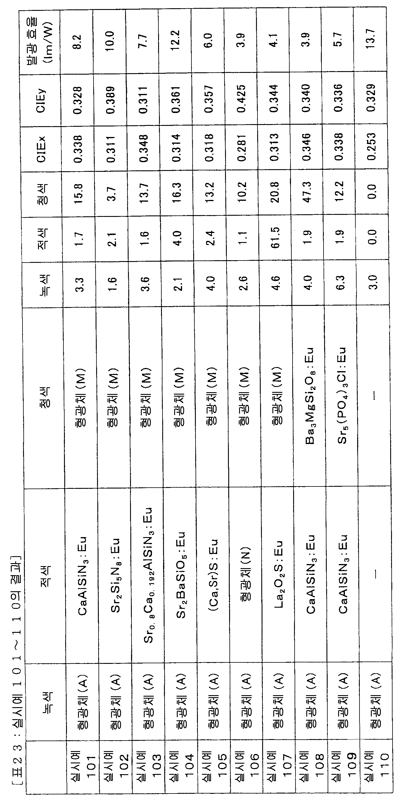
또한, 상기 형광체의 혼합량은, 실리콘 수지, 경화제 및 에어로실의 합계 중량비 (100) 에 대한 각 형광체의 중량비이다.In addition, the mixing amount of the said fluorescent substance is the weight ratio of each fluorescent substance with respect to the
또, 상기 표 23 중의 적색 형광체 (N) 인, Eu(DBM)3Phen (식 중, DBM 은 디벤조일메탄, Phen 은 1,10-페난트롤린을 나타낸다) 의 구조식은 하기와 같다.In addition, the structural formula of Eu (DBM) 3 Phen (wherein DBM represents dibenzoylmethane and Phen represents 1,10-phenanthroline), which is a red phosphor (N) in Table 23, is as follows.
[화학식 1][Formula 1]

(실시예 111 ∼ 120)(Examples 111 to 120)
백색 발광 장치의 색미를 전구색이 되도록 각 형광체의 혼합량을 변화시킨 것 이외에는 실시예 101 ∼ 110 과 동일하게 하여 발광 장치를 제조하고, 평가하였다. 결과를 표 24 에 나타낸다.The light emitting device was manufactured and evaluated in the same manner as in Examples 101 to 110, except that the mixing amount of each phosphor was changed so that the color taste of the white light emitting device became the bulb color. The results are shown in Table 24.

또한, 상기 형광체의 혼합량은, 실리콘 수지, 경화제 및 에어로실의 합계 중량비 (100) 에 대한 각 형광체의 중량비이다.In addition, the mixing amount of the said fluorescent substance is the weight ratio of each fluorescent substance with respect to the
(실시예 121)(Example 121)
C395MB290 (Cree 제조) 대신에 파워 칩 C395XB900 (Cree 사 제조) 을 사용하고, 형광체 A (녹색 형광체), CaAlSiN3:Eu (적색 형광체) 및 BaMgAl5O17:Eu (청색 형광체) 의 혼합량을 실리콘 수지, 경화제 및 에어로실의 합계 중량비 (100) 에 대해, 각각 13.8 중량%, 3.7 중량% 및 30.7 중량% 로 한 것 이외에는 실시예 101 과 동일하게 하여 백색 발광 장치를 제조하고, 평가하였다. (CIEx, CIEy) 는, (0.401, 0.156) 이고, 발광 효율은 3.1 lm/W 이었다.Instead of C395MB290 (manufactured by Cree), a power chip C395XB900 (manufactured by Cree) was used, and a mixed amount of phosphor A (green phosphor), CaAlSiN 3 : Eu (red phosphor) and BaMgAl 5 O 17 : Eu (blue phosphor) was used. The white light emitting device was manufactured and evaluated in the same manner as in Example 101 except that the
본 발명은 산업상의 임의의 분야에서 사용 가능하고, 특히, 조명, 화상 표시 장치 등의 광을 사용하는 용도에 사용하여 특히 바람직하다.The present invention can be used in any field in the industry, and is particularly preferable for use in the use of light such as illumination and image display devices.
본 발명을 특정한 양태를 사용하여 상세하게 설명하였으나, 본 발명의 의도와 범위를 벗어나지 않고 다양한 변경이 가능한 것은 당업자에게 분명하다.While the invention has been described in detail using specific embodiments, it will be apparent to those skilled in the art that various changes may be made without departing from the spirit and scope of the invention.
또한 본 출원은, 2006년 2월 2일자로 출원된 일본 특허출원 (일본 특허출원 2006-26272), 2006년 11월 7일자로 출원된 일본 특허출원 (일본 특허출원 2006-302031) 및 2007년 2월 2일자로 출원된 일본 특허출원 (일본 특허출원 2007-23824) 에 기초하고 있으며, 그 전체가 인용에 의해 원용된다.In addition, this application is a Japanese patent application filed on February 2, 2006 (Japanese Patent Application 2006-26272), a Japanese patent application filed on November 7, 2006 (Japanese Patent Application 2006-302031) and 2 2007 It is based on the Japanese patent application (Japanese Patent Application No. 2007-23824) filed on February 2, which is incorporated by reference in its entirety.
Claims (27)
Applications Claiming Priority (5)
| Application Number | Priority Date | Filing Date | Title |
|---|---|---|---|
| JPJP-P-2006-00026272 | 2006-02-02 | ||
| JP2006026272 | 2006-02-02 | ||
| JPJP-P-2006-00302031 | 2006-11-07 | ||
| JP2006302031 | 2006-11-07 | ||
| PCT/JP2007/051783 WO2007088966A1 (en) | 2006-02-02 | 2007-02-02 | Complex oxynitride phosphor, light-emitting device using same, image display, illuminating device, phosphor-containing composition and complex oxynitride |
Publications (2)
| Publication Number | Publication Date |
|---|---|
| KR20080089519A KR20080089519A (en) | 2008-10-06 |
| KR101096473B1 true KR101096473B1 (en) | 2011-12-20 |
Family
ID=38327534
Family Applications (1)
| Application Number | Title | Priority Date | Filing Date |
|---|---|---|---|
| KR1020087021367A KR101096473B1 (en) | 2006-02-02 | 2007-02-02 | Complex oxynitride phosphor, light-emitting device using same, image display, illuminating device, phosphor-containing composition and complex oxynitride |
Country Status (7)
| Country | Link |
|---|---|
| US (2) | US20090033201A1 (en) |
| EP (1) | EP1985683B1 (en) |
| JP (3) | JP4238269B2 (en) |
| KR (1) | KR101096473B1 (en) |
| CN (1) | CN101379163B (en) |
| TW (1) | TW200801158A (en) |
| WO (1) | WO2007088966A1 (en) |
Cited By (2)
| Publication number | Priority date | Publication date | Assignee | Title |
|---|---|---|---|---|
| KR101510124B1 (en) | 2013-11-13 | 2015-04-09 | 엘지이노텍 주식회사 | BLUISH GREEN EMITTING PHOSPHORS FOR HIGH COLOR RENDERING AND HIGH EFFICIENT WHITE LEDs AND LEDs USING THE SAME |
| US11886087B2 (en) | 2020-08-11 | 2024-01-30 | Lg Innotek Co., Ltd. | Lighting device and vehicle lamp having same |
Families Citing this family (104)
| Publication number | Priority date | Publication date | Assignee | Title |
|---|---|---|---|---|
| US20060135361A1 (en) * | 2004-12-22 | 2006-06-22 | Markel David P | Markable material |
| US7994702B2 (en) | 2005-04-27 | 2011-08-09 | Prysm, Inc. | Scanning beams displays based on light-emitting screens having phosphors |
| JP2007049114A (en) * | 2005-05-30 | 2007-02-22 | Sharp Corp | Light emitting device and method of manufacturing the same |
| US20090033201A1 (en) * | 2006-02-02 | 2009-02-05 | Mitsubishi Chemical Corporation | Complex oxynitride phosphor, light-emitting device using same, image display, illuminating device, phosphor-containing composition and complex oxynitride |
| WO2007123183A1 (en) | 2006-04-19 | 2007-11-01 | Mitsubishi Chemical Corporation | Color image display device |
| CN101448914B (en) | 2006-05-19 | 2012-10-03 | 三菱化学株式会社 | Nitrogen-containing alloy and method for producing phosphor by using the same |
| JP5517400B2 (en) * | 2006-07-11 | 2014-06-11 | 日本碍子株式会社 | Blue light emitting aluminum nitride material and manufacturing method thereof |
| JP2008050496A (en) * | 2006-08-25 | 2008-03-06 | Sony Corp | Light-emitting composition, light source device and displaying device |
| EP2060616A4 (en) * | 2006-09-15 | 2010-08-04 | Mitsubishi Chem Corp | Phosphor, method for producing the same, phosphor-containing composition, light-emitting device, image display and illuminating device |
| JP5367218B2 (en) | 2006-11-24 | 2013-12-11 | シャープ株式会社 | Method for manufacturing phosphor and method for manufacturing light emitting device |
| US8013506B2 (en) | 2006-12-12 | 2011-09-06 | Prysm, Inc. | Organic compounds for adjusting phosphor chromaticity |
| US7857994B2 (en) | 2007-05-30 | 2010-12-28 | GE Lighting Solutions, LLC | Green emitting phosphors and blends thereof |
| JP5710089B2 (en) * | 2007-06-25 | 2015-04-30 | 三星電子株式会社Samsung Electronics Co.,Ltd. | Green light emitting oxynitride phosphor and light emitting device using the same |
| WO2009008250A1 (en) | 2007-07-09 | 2009-01-15 | Sharp Kabushiki Kaisha | Group of phosphor particles, and light-emitting device using the same |
| JP5071709B2 (en) * | 2007-07-17 | 2012-11-14 | 独立行政法人物質・材料研究機構 | Phosphors and light emitting devices |
| DE102007035592B4 (en) | 2007-07-30 | 2023-05-04 | Osram Gmbh | Temperature-stable phosphor, use of a phosphor and method for producing a phosphor |
| EP2180031A4 (en) | 2007-08-01 | 2011-05-25 | Mitsubishi Chem Corp | Phosphor and method for producing the same, crystalline silicon nitride and method for producing the same, phosphor-containing composition, light-emitting device using the phosphor, image display device, and illuminating device |
| JP2009040944A (en) * | 2007-08-10 | 2009-02-26 | Mitsubishi Chemicals Corp | Phosphor, phosphor-containing composition, light emitter, lighting apparatus, and image display device |
| US7597441B1 (en) * | 2007-10-09 | 2009-10-06 | Farwig Michael J | Polarized contrast enhancing sunglass lens |
| EP2242119A4 (en) | 2008-02-07 | 2012-03-07 | Mitsubishi Chem Corp | Semiconductor light emitting device, backlighting device, color image display device and phosphor used for those devices |
| JPWO2009110285A1 (en) | 2008-03-03 | 2011-07-14 | シャープ株式会社 | Light emitting device |
| US8274215B2 (en) | 2008-12-15 | 2012-09-25 | Intematix Corporation | Nitride-based, red-emitting phosphors |
| JP2010196049A (en) * | 2009-01-30 | 2010-09-09 | Mitsubishi Chemicals Corp | Phosphor and method for producing the same, phosphor-containing composition, and light-emitting device, image display device and lighting device using the phosphor |
| US9000664B2 (en) | 2009-04-06 | 2015-04-07 | Sharp Kabushiki Kaisha | Phosphor particle group, light emitting apparatus using the same, and liquid crystal display television |
| EP2449056A1 (en) | 2009-07-02 | 2012-05-09 | Koninklijke Philips Electronics N.V. | Green emitting material |
| WO2011002087A1 (en) | 2009-07-02 | 2011-01-06 | シャープ株式会社 | Light-emitting device |
| WO2011014010A2 (en) * | 2009-07-28 | 2011-02-03 | 성균관대학교산학협력단 | Oxynitride phosphor powder, nitride phosphor powder and a production method therefor |
| KR101172143B1 (en) * | 2009-08-10 | 2012-08-07 | 엘지이노텍 주식회사 | OXYNITRIDE-BASED PHOSPHORS COMPOSING OF SiON ELEMENT FOR WHITE LEDs, MANUFACTURING METHOD THEREOF AND LEDs USING THE SAME |
| WO2011024818A1 (en) * | 2009-08-26 | 2011-03-03 | 三菱化学株式会社 | Semiconductor white light-emitting device |
| JP5129392B2 (en) * | 2009-08-28 | 2013-01-30 | 株式会社東芝 | Method for producing phosphor and phosphor produced thereby |
| KR101163902B1 (en) * | 2010-08-10 | 2012-07-09 | 엘지이노텍 주식회사 | Light emitting device |
| WO2011028033A2 (en) | 2009-09-02 | 2011-03-10 | 엘지이노텍주식회사 | Phosphor, preparation method of phosphor, and white light emitting device |
| CN102471684B (en) * | 2009-09-18 | 2014-10-01 | 三井金属矿业株式会社 | Phosphor |
| KR100958700B1 (en) * | 2009-09-21 | 2010-05-18 | 금호전기주식회사 | Oxynitride phosphor, method for manufacturing the same and light-emitting device comprising the same |
| WO2011042830A2 (en) * | 2009-10-09 | 2011-04-14 | Koninklijke Philips Electronics N.V. | High efficiency lighting assembly |
| US8324794B2 (en) | 2009-12-10 | 2012-12-04 | Panasonic Corporation | Plasma display device |
| JP5748769B2 (en) * | 2009-12-21 | 2015-07-15 | ソウル セミコンダクター カンパニー リミテッド | Light emitting device having phosphor of strontium oxyorthosilicate type |
| EP2468836A4 (en) | 2010-01-08 | 2014-07-30 | Sharp Kk | Phosphor, light-emitting device, and liquid crystal display device using same |
| JP5190475B2 (en) * | 2010-02-19 | 2013-04-24 | 株式会社東芝 | Phosphor and light emitting device using the same |
| DE102010008839B4 (en) * | 2010-02-22 | 2016-04-21 | Spectro Analytical Instruments Gmbh | Method for the determination of carbon in cast iron |
| KR20120120353A (en) * | 2010-02-24 | 2012-11-01 | 제이에스알 가부시끼가이샤 | Color filter and color liquid crystal display element |
| EP2540798A4 (en) | 2010-02-26 | 2014-04-30 | Mitsubishi Chem Corp | Halophosphate phosphor and white light emitting device |
| EP2541630B1 (en) | 2010-02-26 | 2017-05-31 | Sharp Kabushiki Kaisha | Light-emitting device |
| JP4930649B1 (en) | 2011-02-25 | 2012-05-16 | 三菱化学株式会社 | Halophosphate phosphor and white light emitting device |
| CN101781560B (en) * | 2010-03-23 | 2012-11-14 | 中国计量学院 | Fluorescent powder using silicon-aluminum base nitrogen oxides as base materials and preparation method thereof |
| WO2011122655A1 (en) | 2010-03-30 | 2011-10-06 | 三菱化学株式会社 | Light-emitting device |
| CN102823002A (en) | 2010-03-30 | 2012-12-12 | 三菱化学株式会社 | Light-emitting device |
| US8764210B2 (en) | 2010-07-19 | 2014-07-01 | Greenwave Reality Pte Ltd. | Emitting light using multiple phosphors |
| US8820981B2 (en) | 2010-07-19 | 2014-09-02 | Greenwave Reality Pte Ltd | Electrically controlled glass in a lamp |
| US20120019126A1 (en) * | 2010-07-22 | 2012-01-26 | General Electric Company | Oxynitride phosphors, method of preparation, and light emitting instrument |
| JP5783512B2 (en) | 2010-07-26 | 2015-09-24 | シャープ株式会社 | Light emitting device |
| US7976727B1 (en) * | 2010-08-25 | 2011-07-12 | The United States Of America As Represented By The Secretary Of The Air Force | Chromium-doped zinc-nitro-antimony-gallium-tellurium infrared phosphors |
| EP2428543B1 (en) | 2010-09-08 | 2013-05-08 | Kabushiki Kaisha Toshiba | Light emitting device |
| KR101196207B1 (en) * | 2010-11-05 | 2012-11-05 | 조성매 | Green light-emitting diode by phosphor |
| CN102559182A (en) * | 2010-12-16 | 2012-07-11 | 中国科学院福建物质结构研究所 | Novel white-light nano-luminescent material of yttrium aluminate activated by dysprosium |
| CN103328608B (en) | 2011-01-18 | 2015-04-22 | 夏普株式会社 | Semiconductor light-emitting device |
| TWI431097B (en) * | 2011-07-05 | 2014-03-21 | Formosa Epitaxy Inc | Nitrogen oxide phosphor and a method for producing the same |
| TWI538979B (en) * | 2011-07-05 | 2016-06-21 | Formosa Epitaxy Inc | Production method of nitrogen oxide fluorescent powder |
| TWI452116B (en) * | 2011-07-05 | 2014-09-11 | Formosa Epitaxy Inc | Nitrogen oxide phosphor and a method for producing the same |
| DE112011103246B4 (en) | 2011-09-29 | 2021-09-23 | Beijing Yuji Science And Technology Co. Ltd | Nitride phosphors |
| KR101863548B1 (en) * | 2011-11-23 | 2018-06-05 | 삼성전자주식회사 | Oxinitride phosphor and light emitting device comprising the same |
| KR101877423B1 (en) * | 2011-11-28 | 2018-07-11 | 엘지이노텍 주식회사 | Oxynitride phosphor, and light-emitting device package comprising the same |
| JP5972571B2 (en) * | 2011-12-28 | 2016-08-17 | 日東電工株式会社 | Optical semiconductor device and lighting device |
| US8663502B2 (en) | 2011-12-30 | 2014-03-04 | Intematix Corporation | Red-emitting nitride-based phosphors |
| WO2013102222A1 (en) | 2011-12-30 | 2013-07-04 | Intematix Corporation | Nitride phosphors with interstitial cations for charge balance |
| JP2013163723A (en) * | 2012-02-09 | 2013-08-22 | Denki Kagaku Kogyo Kk | Phosphor and light-emitting device |
| JP2013163725A (en) * | 2012-02-09 | 2013-08-22 | Denki Kagaku Kogyo Kk | Phosphor and light-emitting device |
| JP2013163722A (en) * | 2012-02-09 | 2013-08-22 | Denki Kagaku Kogyo Kk | Phosphor and light-emitting device |
| WO2013147195A1 (en) | 2012-03-30 | 2013-10-03 | 三菱化学株式会社 | Semiconductor light-emitting device, and illumination device |
| CN104024375B (en) * | 2012-05-31 | 2017-05-24 | 国立研究开发法人物质·材料研究机构 | Phosphor, Method For Manufacturing Same, Light Emitting Device, And Image Display Device |
| JP5880300B2 (en) * | 2012-06-14 | 2016-03-08 | 日立化成株式会社 | Adhesive composition and semiconductor device using the same |
| KR101362185B1 (en) * | 2012-06-22 | 2014-02-12 | 순천대학교 산학협력단 | Phospor and light emitting device comprising the phospor |
| US8597545B1 (en) | 2012-07-18 | 2013-12-03 | Intematix Corporation | Red-emitting nitride-based calcium-stabilized phosphors |
| KR101688337B1 (en) * | 2012-07-25 | 2016-12-20 | 코쿠리츠켄큐카이하츠호징 붓시쯔 자이료 켄큐키코 | Fluorophore, method for producing same, light-emitting device using fluorophore, image display device, pigment, and ultraviolet absorbent |
| CN102994079A (en) * | 2012-12-21 | 2013-03-27 | 北京有色金属研究总院 | Nitrogen-oxide orange-red fluorescent material comprising light-emitting film or light-emitting piece and light-emitting device |
| TWI483902B (en) * | 2013-04-03 | 2015-05-11 | 國立臺灣大學 | Method for fabricating metal-ion-doped zinc sulfide and method for generating a warm white light by using the metal-ion-doped zinc sulfide |
| TWI468842B (en) * | 2013-05-07 | 2015-01-11 | Delta Electronics Inc | Method of regulating light wavelength for projection device |
| CN103351863B (en) * | 2013-07-08 | 2015-10-28 | 江苏博睿光电有限公司 | Red fluorescent powder and preparation method thereof |
| JP2015088483A (en) * | 2013-09-26 | 2015-05-07 | 信越化学工業株式会社 | Red color lamp and light device for vehicle |
| US10069046B2 (en) * | 2013-11-13 | 2018-09-04 | Lg Innotek Co., Ltd. | Bluish green phosphor and light emitting device package including the same |
| EP3091585A4 (en) * | 2013-12-27 | 2017-07-26 | Citizen Electronics Co., Ltd | Light-emitting device and method for designing light emitting device |
| US10014451B2 (en) | 2014-02-18 | 2018-07-03 | Sumitomo Chemical Company, Limited | Method for producing semiconductor light-emitting device |
| CA2944454A1 (en) | 2014-04-01 | 2015-10-08 | The Research Foundation For The State University Of New York | Electrode materials for group ii cation-based batteries |
| US9315725B2 (en) * | 2014-08-28 | 2016-04-19 | Lightscape Materials, Inc. | Method of making EU2+ activated inorganic red phosphor |
| CN106795429B (en) | 2014-10-23 | 2020-06-12 | 三菱化学株式会社 | Phosphor, light emitting device, illumination device, and image display device |
| WO2016134995A1 (en) * | 2015-02-23 | 2016-09-01 | Koninklijke Philips N.V. | White phosphor converted led with stable flux output versus temperature |
| KR102415650B1 (en) | 2015-03-18 | 2022-07-01 | 엘지전자 주식회사 | Oxy-nitride phosphor and light emitting device package |
| KR102415649B1 (en) | 2015-03-18 | 2022-07-01 | 엘지전자 주식회사 | Oxy-nitride phosphor and light emitting device package |
| US10658552B2 (en) * | 2015-03-24 | 2020-05-19 | Koninklijke Philips N.V. | Blue emitting phosphor converted LED with blue pigment |
| WO2016198395A1 (en) * | 2015-06-08 | 2016-12-15 | Osram Opto Semiconductors Gmbh | Composite oxynitride ceramic converter and light source having same |
| DE102015110258A1 (en) * | 2015-06-25 | 2016-12-29 | Osram Gmbh | Phosphor, method for producing a phosphor and use of a phosphor |
| JP6641824B2 (en) * | 2015-09-16 | 2020-02-05 | 日亜化学工業株式会社 | Light emitting device |
| WO2017111495A1 (en) * | 2015-12-23 | 2017-06-29 | 엘지이노텍 주식회사 | Phosphor composition, light-emitting device package comprising same, and lighting apparatus |
| CN106816489A (en) * | 2017-02-28 | 2017-06-09 | 安徽拓吉泰新型陶瓷科技有限公司 | A kind of light sensitive resistance ceramics and preparation method thereof |
| KR20190058599A (en) | 2017-09-28 | 2019-05-29 | 루미리즈 홀딩 비.브이. | Wavelength conversion material for light emitting device |
| JPWO2019164014A1 (en) * | 2018-02-26 | 2021-02-04 | 京セラ株式会社 | Light emitting device and lighting device |
| CN108485655A (en) * | 2018-04-04 | 2018-09-04 | 陕西师范大学 | Ca4Si4N2O9Crystal and fluorescent powder and preparation method |
| JP7204380B2 (en) * | 2018-08-28 | 2023-01-16 | 株式会社ディスコ | table |
| KR20210141557A (en) * | 2019-04-03 | 2021-11-23 | 코쿠리츠켄큐카이하츠호징 붓시쯔 자이료 켄큐키코 | Phosphor, its manufacturing method and light emitting device |
| KR20220001788A (en) * | 2020-06-30 | 2022-01-06 | 엘지디스플레이 주식회사 | Display apparatus and manufacturing of the same |
| EP4354544A1 (en) * | 2021-05-27 | 2024-04-17 | Sino Applied Technology Taiwan Co., Ltd. | Anode active substance and preparation method therefor, and lithium secondary battery prepared on basis of same |
| CN114084880B (en) * | 2021-10-19 | 2023-05-09 | 中国科学院福建物质结构研究所 | K 3 Sc 3 (PO 4 )(PO 3 F) 2 F 5 Compound, nonlinear optical crystal, and preparation method and application thereof |
| DE102022125141A1 (en) | 2022-09-29 | 2024-04-04 | Schott Ag | Lighting system with optimized color scale |
| CN116574505A (en) * | 2023-04-27 | 2023-08-11 | 桂林电子科技大学 | Preparation method of gallate stress luminescent material |
Citations (3)
| Publication number | Priority date | Publication date | Assignee | Title |
|---|---|---|---|---|
| JP2003206481A (en) | 2001-09-25 | 2003-07-22 | Patent Treuhand Ges Elektr Gluehlamp Mbh | Illumination unit having at least one led as light source |
| JP2005200584A (en) | 2004-01-16 | 2005-07-28 | Mitsubishi Chemicals Corp | Fluorescent substance, light emitting system, iluminating system and image-displaying system using the same |
| JP2005281700A (en) | 2002-10-16 | 2005-10-13 | Nichia Chem Ind Ltd | Light-emitting device using oxynitride fluorophor |
Family Cites Families (21)
| Publication number | Priority date | Publication date | Assignee | Title |
|---|---|---|---|---|
| US6809781B2 (en) * | 2002-09-24 | 2004-10-26 | General Electric Company | Phosphor blends and backlight sources for liquid crystal displays |
| EP1413619A1 (en) | 2002-09-24 | 2004-04-28 | Osram Opto Semiconductors GmbH | Luminescent material, especially for LED application |
| EP1413618A1 (en) | 2002-09-24 | 2004-04-28 | Osram Opto Semiconductors GmbH | Luminescent material, especially for LED application |
| US6717353B1 (en) * | 2002-10-14 | 2004-04-06 | Lumileds Lighting U.S., Llc | Phosphor converted light emitting device |
| WO2004036962A1 (en) * | 2002-10-14 | 2004-04-29 | Philips Intellectual Property & Standards Gmbh | Light-emitting device comprising an eu(ii)-activated phosphor |
| MY149573A (en) | 2002-10-16 | 2013-09-13 | Nichia Corp | Oxynitride phosphor and production process thereof, and light-emitting device using oxynitride phosphor |
| JP4442101B2 (en) * | 2003-03-14 | 2010-03-31 | 日亜化学工業株式会社 | Oxynitride phosphor and light emitting device using the same |
| JP4415547B2 (en) * | 2002-10-16 | 2010-02-17 | 日亜化学工業株式会社 | Oxynitride phosphor and method for producing the same |
| AU2003277627A1 (en) * | 2002-11-08 | 2004-06-07 | Nichia Corporation | Light emitting device, phosphor and method for preparing phosphor |
| US7923918B2 (en) * | 2003-03-13 | 2011-04-12 | Nichia Corporation | Light emitting film, luminescent device, method for manufacturing light emitting film and method for manufacturing luminescent device |
| JP2005093912A (en) * | 2003-09-19 | 2005-04-07 | Nichia Chem Ind Ltd | Light-emitting device |
| TW200523340A (en) * | 2003-09-24 | 2005-07-16 | Patent Treuhand Ges Fur Elek Sche Gluhlampen Mbh | Hochefeizienter leuchtstoff |
| CN1886483B (en) * | 2003-09-24 | 2010-06-16 | 电灯专利信托有限公司 | Highly efficient LED-based illumination system featuring improved color rendering |
| JP4834827B2 (en) * | 2003-10-03 | 2011-12-14 | 独立行政法人物質・材料研究機構 | Oxynitride phosphor |
| JP2005298721A (en) * | 2004-04-14 | 2005-10-27 | Nichia Chem Ind Ltd | Oxynitride phosphor and light emitting device using the same |
| US7229573B2 (en) * | 2004-04-20 | 2007-06-12 | Gelcore, Llc | Ce3+ and Eu2+ doped phosphors for light generation |
| US7439668B2 (en) * | 2005-03-01 | 2008-10-21 | Lumination Llc | Oxynitride phosphors for use in lighting applications having improved color quality |
| US20090033201A1 (en) * | 2006-02-02 | 2009-02-05 | Mitsubishi Chemical Corporation | Complex oxynitride phosphor, light-emitting device using same, image display, illuminating device, phosphor-containing composition and complex oxynitride |
| CN101379164B (en) * | 2006-02-10 | 2012-11-21 | 三菱化学株式会社 | Phosphor, method for producing same, phosphor-containing composition, light-emitting device, image display, and illuminating device |
| US7857994B2 (en) * | 2007-05-30 | 2010-12-28 | GE Lighting Solutions, LLC | Green emitting phosphors and blends thereof |
| DE102007035592B4 (en) | 2007-07-30 | 2023-05-04 | Osram Gmbh | Temperature-stable phosphor, use of a phosphor and method for producing a phosphor |
-
2007
- 2007-02-02 US US12/278,220 patent/US20090033201A1/en not_active Abandoned
- 2007-02-02 TW TW096103822A patent/TW200801158A/en not_active IP Right Cessation
- 2007-02-02 EP EP07713780.0A patent/EP1985683B1/en not_active Expired - Fee Related
- 2007-02-02 WO PCT/JP2007/051783 patent/WO2007088966A1/en active Application Filing
- 2007-02-02 KR KR1020087021367A patent/KR101096473B1/en not_active IP Right Cessation
- 2007-02-02 JP JP2007023824A patent/JP4238269B2/en not_active Expired - Fee Related
- 2007-02-02 CN CN2007800042483A patent/CN101379163B/en not_active Expired - Fee Related
-
2008
- 2008-04-14 JP JP2008105093A patent/JP5176665B2/en not_active Expired - Fee Related
-
2009
- 2009-03-09 US US12/400,188 patent/US7833436B2/en not_active Expired - Fee Related
-
2012
- 2012-11-22 JP JP2012256140A patent/JP5365735B2/en not_active Expired - Fee Related
Patent Citations (3)
| Publication number | Priority date | Publication date | Assignee | Title |
|---|---|---|---|---|
| JP2003206481A (en) | 2001-09-25 | 2003-07-22 | Patent Treuhand Ges Elektr Gluehlamp Mbh | Illumination unit having at least one led as light source |
| JP2005281700A (en) | 2002-10-16 | 2005-10-13 | Nichia Chem Ind Ltd | Light-emitting device using oxynitride fluorophor |
| JP2005200584A (en) | 2004-01-16 | 2005-07-28 | Mitsubishi Chemicals Corp | Fluorescent substance, light emitting system, iluminating system and image-displaying system using the same |
Cited By (2)
| Publication number | Priority date | Publication date | Assignee | Title |
|---|---|---|---|---|
| KR101510124B1 (en) | 2013-11-13 | 2015-04-09 | 엘지이노텍 주식회사 | BLUISH GREEN EMITTING PHOSPHORS FOR HIGH COLOR RENDERING AND HIGH EFFICIENT WHITE LEDs AND LEDs USING THE SAME |
| US11886087B2 (en) | 2020-08-11 | 2024-01-30 | Lg Innotek Co., Ltd. | Lighting device and vehicle lamp having same |
Also Published As
| Publication number | Publication date |
|---|---|
| US20090033201A1 (en) | 2009-02-05 |
| TWI370840B (en) | 2012-08-21 |
| CN101379163A (en) | 2009-03-04 |
| JP2013065877A (en) | 2013-04-11 |
| WO2007088966A1 (en) | 2007-08-09 |
| TW200801158A (en) | 2008-01-01 |
| JP5176665B2 (en) | 2013-04-03 |
| EP1985683B1 (en) | 2013-08-28 |
| US7833436B2 (en) | 2010-11-16 |
| JP2008199053A (en) | 2008-08-28 |
| KR20080089519A (en) | 2008-10-06 |
| EP1985683A4 (en) | 2011-05-11 |
| EP1985683A1 (en) | 2008-10-29 |
| JP2008138156A (en) | 2008-06-19 |
| JP4238269B2 (en) | 2009-03-18 |
| US20090166584A1 (en) | 2009-07-02 |
| CN101379163B (en) | 2013-01-02 |
| JP5365735B2 (en) | 2013-12-11 |
Similar Documents
| Publication | Publication Date | Title |
|---|---|---|
| KR101096473B1 (en) | Complex oxynitride phosphor, light-emitting device using same, image display, illuminating device, phosphor-containing composition and complex oxynitride | |
| KR101184957B1 (en) | Phosphor, method for producing same, phosphor-containing composition, light-emitting device, image display, and illuminating device | |
| JP4466757B2 (en) | Phosphor, phosphor-containing composition, light emitting device, lighting device, image display device, and nitrogen-containing compound | |
| JP5245222B2 (en) | Phosphor and light emitting device using the same | |
| EP2141215A1 (en) | Phosphor and method for producing the same, phosphor-containing composition, light-emitting device, image display device, and illuminating device | |
| JP5200741B2 (en) | Crystalline silicon nitride and method for producing the same, and phosphor using the same, phosphor-containing composition, light emitting device, lighting device, image display device, sintered body, and pigment | |
| WO2007018260A1 (en) | Phosphor and light-emitting device using same | |
| JP2009263610A (en) | Phosphor and method for producing the same, crystalline silicon nitride and method for producing the same, phosphor-containing composition, light-emitting device using the phosphor, image display device, and illuminating device | |
| JP2008285662A (en) | Method for producing inorganic substance, phosphor, phosphor-including composition, emission device, illumination device, and image display device | |
| JP2009057554A (en) | Method for producing fluorescent material, fluorescent material obtained by the same, fluorescent material-containing composition using the fluorescent material, light emitting device, lighting device and image display device | |
| JP2008095091A (en) | Fluorescent substance and its production method, fluorescent substance containing composition, light emitting device, image display device, and illuminating device | |
| JP2009040918A (en) | Fluorescent substance and its production method, composition containing fluorescent substance, light emitting device, and image display and illuminating device | |
| JP2009040944A (en) | Phosphor, phosphor-containing composition, light emitter, lighting apparatus, and image display device | |
| JP2009161576A (en) | Fluorescent substance and light emitting apparatus using it | |
| JP2008266410A (en) | Fluorescent substance, fluorescent substance-containing composition, manufacturing method of fluorescent substance, light emitting apparatus, image display device, and illuminating device | |
| JP2009203466A (en) | Fluorescent substance, composition containing fluorescent substance, light emitter, image display device, and illuminating device | |
| JP5251140B2 (en) | Phosphor, phosphor-containing composition, light emitting device, image display device, and illumination device | |
| JP5590092B2 (en) | Phosphor, phosphor-containing composition, light emitting device, image display device and lighting device | |
| JP2009126891A (en) | Oxide fluorophor and its production method, and fluorophor-containing composition, light-emitting device, image display device and illuminating device |
Legal Events
| Date | Code | Title | Description |
|---|---|---|---|
| A201 | Request for examination | ||
| E902 | Notification of reason for refusal | ||
| E701 | Decision to grant or registration of patent right | ||
| GRNT | Written decision to grant | ||
| FPAY | Annual fee payment |
Payment date: 20141120 Year of fee payment: 4 |
|
| FPAY | Annual fee payment |
Payment date: 20151118 Year of fee payment: 5 |
|
| FPAY | Annual fee payment |
Payment date: 20161123 Year of fee payment: 6 |
|
| FPAY | Annual fee payment |
Payment date: 20171117 Year of fee payment: 7 |
|
| LAPS | Lapse due to unpaid annual fee |