KR100755089B1 - Data storage media - Google Patents
Data storage media Download PDFInfo
- Publication number
- KR100755089B1 KR100755089B1 KR1020017010138A KR20017010138A KR100755089B1 KR 100755089 B1 KR100755089 B1 KR 100755089B1 KR 1020017010138 A KR1020017010138 A KR 1020017010138A KR 20017010138 A KR20017010138 A KR 20017010138A KR 100755089 B1 KR100755089 B1 KR 100755089B1
- Authority
- KR
- South Korea
- Prior art keywords
- delete delete
- substrate
- storage medium
- data
- plastic
- Prior art date
Links
Images


Classifications
-
- B—PERFORMING OPERATIONS; TRANSPORTING
- B82—NANOTECHNOLOGY
- B82Y—SPECIFIC USES OR APPLICATIONS OF NANOSTRUCTURES; MEASUREMENT OR ANALYSIS OF NANOSTRUCTURES; MANUFACTURE OR TREATMENT OF NANOSTRUCTURES
- B82Y30/00—Nanotechnology for materials or surface science, e.g. nanocomposites
-
- B—PERFORMING OPERATIONS; TRANSPORTING
- B29—WORKING OF PLASTICS; WORKING OF SUBSTANCES IN A PLASTIC STATE IN GENERAL
- B29C—SHAPING OR JOINING OF PLASTICS; SHAPING OF MATERIAL IN A PLASTIC STATE, NOT OTHERWISE PROVIDED FOR; AFTER-TREATMENT OF THE SHAPED PRODUCTS, e.g. REPAIRING
- B29C43/00—Compression moulding, i.e. applying external pressure to flow the moulding material; Apparatus therefor
- B29C43/02—Compression moulding, i.e. applying external pressure to flow the moulding material; Apparatus therefor of articles of definite length, i.e. discrete articles
- B29C43/021—Compression moulding, i.e. applying external pressure to flow the moulding material; Apparatus therefor of articles of definite length, i.e. discrete articles characterised by the shape of the surface
-
- B—PERFORMING OPERATIONS; TRANSPORTING
- B29—WORKING OF PLASTICS; WORKING OF SUBSTANCES IN A PLASTIC STATE IN GENERAL
- B29D—PRODUCING PARTICULAR ARTICLES FROM PLASTICS OR FROM SUBSTANCES IN A PLASTIC STATE
- B29D17/00—Producing carriers of records containing fine grooves or impressions, e.g. disc records for needle playback, cylinder records; Producing record discs from master stencils
- B29D17/005—Producing optically read record carriers, e.g. optical discs
-
- B—PERFORMING OPERATIONS; TRANSPORTING
- B82—NANOTECHNOLOGY
- B82Y—SPECIFIC USES OR APPLICATIONS OF NANOSTRUCTURES; MEASUREMENT OR ANALYSIS OF NANOSTRUCTURES; MANUFACTURE OR TREATMENT OF NANOSTRUCTURES
- B82Y10/00—Nanotechnology for information processing, storage or transmission, e.g. quantum computing or single electron logic
-
- G—PHYSICS
- G11—INFORMATION STORAGE
- G11B—INFORMATION STORAGE BASED ON RELATIVE MOVEMENT BETWEEN RECORD CARRIER AND TRANSDUCER
- G11B11/00—Recording on or reproducing from the same record carrier wherein for these two operations the methods are covered by different main groups of groups G11B3/00 - G11B7/00 or by different subgroups of group G11B9/00; Record carriers therefor
- G11B11/10—Recording on or reproducing from the same record carrier wherein for these two operations the methods are covered by different main groups of groups G11B3/00 - G11B7/00 or by different subgroups of group G11B9/00; Record carriers therefor using recording by magnetic means or other means for magnetisation or demagnetisation of a record carrier, e.g. light induced spin magnetisation; Demagnetisation by thermal or stress means in the presence or not of an orienting magnetic field
- G11B11/105—Recording on or reproducing from the same record carrier wherein for these two operations the methods are covered by different main groups of groups G11B3/00 - G11B7/00 or by different subgroups of group G11B9/00; Record carriers therefor using recording by magnetic means or other means for magnetisation or demagnetisation of a record carrier, e.g. light induced spin magnetisation; Demagnetisation by thermal or stress means in the presence or not of an orienting magnetic field using a beam of light or a magnetic field for recording by change of magnetisation and a beam of light for reproducing, i.e. magneto-optical, e.g. light-induced thermomagnetic recording, spin magnetisation recording, Kerr or Faraday effect reproducing
- G11B11/10582—Record carriers characterised by the selection of the material or by the structure or form
- G11B11/10584—Record carriers characterised by the selection of the material or by the structure or form characterised by the form, e.g. comprising mechanical protection elements
-
- G—PHYSICS
- G11—INFORMATION STORAGE
- G11B—INFORMATION STORAGE BASED ON RELATIVE MOVEMENT BETWEEN RECORD CARRIER AND TRANSDUCER
- G11B11/00—Recording on or reproducing from the same record carrier wherein for these two operations the methods are covered by different main groups of groups G11B3/00 - G11B7/00 or by different subgroups of group G11B9/00; Record carriers therefor
- G11B11/10—Recording on or reproducing from the same record carrier wherein for these two operations the methods are covered by different main groups of groups G11B3/00 - G11B7/00 or by different subgroups of group G11B9/00; Record carriers therefor using recording by magnetic means or other means for magnetisation or demagnetisation of a record carrier, e.g. light induced spin magnetisation; Demagnetisation by thermal or stress means in the presence or not of an orienting magnetic field
- G11B11/105—Recording on or reproducing from the same record carrier wherein for these two operations the methods are covered by different main groups of groups G11B3/00 - G11B7/00 or by different subgroups of group G11B9/00; Record carriers therefor using recording by magnetic means or other means for magnetisation or demagnetisation of a record carrier, e.g. light induced spin magnetisation; Demagnetisation by thermal or stress means in the presence or not of an orienting magnetic field using a beam of light or a magnetic field for recording by change of magnetisation and a beam of light for reproducing, i.e. magneto-optical, e.g. light-induced thermomagnetic recording, spin magnetisation recording, Kerr or Faraday effect reproducing
- G11B11/10582—Record carriers characterised by the selection of the material or by the structure or form
- G11B11/10586—Record carriers characterised by the selection of the material or by the structure or form characterised by the selection of the material
-
- G—PHYSICS
- G11—INFORMATION STORAGE
- G11B—INFORMATION STORAGE BASED ON RELATIVE MOVEMENT BETWEEN RECORD CARRIER AND TRANSDUCER
- G11B5/00—Recording by magnetisation or demagnetisation of a record carrier; Reproducing by magnetic means; Record carriers therefor
- G11B5/62—Record carriers characterised by the selection of the material
- G11B5/72—Protective coatings, e.g. anti-static or antifriction
-
- G—PHYSICS
- G11—INFORMATION STORAGE
- G11B—INFORMATION STORAGE BASED ON RELATIVE MOVEMENT BETWEEN RECORD CARRIER AND TRANSDUCER
- G11B5/00—Recording by magnetisation or demagnetisation of a record carrier; Reproducing by magnetic means; Record carriers therefor
- G11B5/62—Record carriers characterised by the selection of the material
- G11B5/73—Base layers, i.e. all non-magnetic layers lying under a lowermost magnetic recording layer, e.g. including any non-magnetic layer in between a first magnetic recording layer and either an underlying substrate or a soft magnetic underlayer
- G11B5/739—Magnetic recording media substrates
- G11B5/73911—Inorganic substrates
- G11B5/73913—Composites or coated substrates
-
- G—PHYSICS
- G11—INFORMATION STORAGE
- G11B—INFORMATION STORAGE BASED ON RELATIVE MOVEMENT BETWEEN RECORD CARRIER AND TRANSDUCER
- G11B5/00—Recording by magnetisation or demagnetisation of a record carrier; Reproducing by magnetic means; Record carriers therefor
- G11B5/62—Record carriers characterised by the selection of the material
- G11B5/73—Base layers, i.e. all non-magnetic layers lying under a lowermost magnetic recording layer, e.g. including any non-magnetic layer in between a first magnetic recording layer and either an underlying substrate or a soft magnetic underlayer
- G11B5/739—Magnetic recording media substrates
- G11B5/73911—Inorganic substrates
- G11B5/73917—Metallic substrates, i.e. elemental metal or metal alloy substrates
- G11B5/73919—Aluminium or titanium elemental or alloy substrates
-
- G—PHYSICS
- G11—INFORMATION STORAGE
- G11B—INFORMATION STORAGE BASED ON RELATIVE MOVEMENT BETWEEN RECORD CARRIER AND TRANSDUCER
- G11B5/00—Recording by magnetisation or demagnetisation of a record carrier; Reproducing by magnetic means; Record carriers therefor
- G11B5/62—Record carriers characterised by the selection of the material
- G11B5/73—Base layers, i.e. all non-magnetic layers lying under a lowermost magnetic recording layer, e.g. including any non-magnetic layer in between a first magnetic recording layer and either an underlying substrate or a soft magnetic underlayer
- G11B5/739—Magnetic recording media substrates
- G11B5/73911—Inorganic substrates
- G11B5/73921—Glass or ceramic substrates
-
- G—PHYSICS
- G11—INFORMATION STORAGE
- G11B—INFORMATION STORAGE BASED ON RELATIVE MOVEMENT BETWEEN RECORD CARRIER AND TRANSDUCER
- G11B5/00—Recording by magnetisation or demagnetisation of a record carrier; Reproducing by magnetic means; Record carriers therefor
- G11B5/84—Processes or apparatus specially adapted for manufacturing record carriers
- G11B5/8404—Processes or apparatus specially adapted for manufacturing record carriers manufacturing base layers
-
- G—PHYSICS
- G11—INFORMATION STORAGE
- G11B—INFORMATION STORAGE BASED ON RELATIVE MOVEMENT BETWEEN RECORD CARRIER AND TRANSDUCER
- G11B5/00—Recording by magnetisation or demagnetisation of a record carrier; Reproducing by magnetic means; Record carriers therefor
- G11B5/84—Processes or apparatus specially adapted for manufacturing record carriers
- G11B5/855—Coating only part of a support with a magnetic layer
-
- G—PHYSICS
- G11—INFORMATION STORAGE
- G11B—INFORMATION STORAGE BASED ON RELATIVE MOVEMENT BETWEEN RECORD CARRIER AND TRANSDUCER
- G11B7/00—Recording or reproducing by optical means, e.g. recording using a thermal beam of optical radiation by modifying optical properties or the physical structure, reproducing using an optical beam at lower power by sensing optical properties; Record carriers therefor
- G11B7/24—Record carriers characterised by shape, structure or physical properties, or by the selection of the material
- G11B7/2403—Layers; Shape, structure or physical properties thereof
- G11B7/24047—Substrates
-
- G—PHYSICS
- G11—INFORMATION STORAGE
- G11B—INFORMATION STORAGE BASED ON RELATIVE MOVEMENT BETWEEN RECORD CARRIER AND TRANSDUCER
- G11B7/00—Recording or reproducing by optical means, e.g. recording using a thermal beam of optical radiation by modifying optical properties or the physical structure, reproducing using an optical beam at lower power by sensing optical properties; Record carriers therefor
- G11B7/24—Record carriers characterised by shape, structure or physical properties, or by the selection of the material
- G11B7/241—Record carriers characterised by shape, structure or physical properties, or by the selection of the material characterised by the selection of the material
- G11B7/252—Record carriers characterised by shape, structure or physical properties, or by the selection of the material characterised by the selection of the material of layers other than recording layers
- G11B7/253—Record carriers characterised by shape, structure or physical properties, or by the selection of the material characterised by the selection of the material of layers other than recording layers of substrates
- G11B7/2531—Record carriers characterised by shape, structure or physical properties, or by the selection of the material characterised by the selection of the material of layers other than recording layers of substrates comprising glass
-
- G—PHYSICS
- G11—INFORMATION STORAGE
- G11B—INFORMATION STORAGE BASED ON RELATIVE MOVEMENT BETWEEN RECORD CARRIER AND TRANSDUCER
- G11B7/00—Recording or reproducing by optical means, e.g. recording using a thermal beam of optical radiation by modifying optical properties or the physical structure, reproducing using an optical beam at lower power by sensing optical properties; Record carriers therefor
- G11B7/24—Record carriers characterised by shape, structure or physical properties, or by the selection of the material
- G11B7/241—Record carriers characterised by shape, structure or physical properties, or by the selection of the material characterised by the selection of the material
- G11B7/252—Record carriers characterised by shape, structure or physical properties, or by the selection of the material characterised by the selection of the material of layers other than recording layers
- G11B7/253—Record carriers characterised by shape, structure or physical properties, or by the selection of the material characterised by the selection of the material of layers other than recording layers of substrates
- G11B7/2532—Record carriers characterised by shape, structure or physical properties, or by the selection of the material characterised by the selection of the material of layers other than recording layers of substrates comprising metals
-
- G—PHYSICS
- G11—INFORMATION STORAGE
- G11B—INFORMATION STORAGE BASED ON RELATIVE MOVEMENT BETWEEN RECORD CARRIER AND TRANSDUCER
- G11B7/00—Recording or reproducing by optical means, e.g. recording using a thermal beam of optical radiation by modifying optical properties or the physical structure, reproducing using an optical beam at lower power by sensing optical properties; Record carriers therefor
- G11B7/24—Record carriers characterised by shape, structure or physical properties, or by the selection of the material
- G11B7/241—Record carriers characterised by shape, structure or physical properties, or by the selection of the material characterised by the selection of the material
- G11B7/252—Record carriers characterised by shape, structure or physical properties, or by the selection of the material characterised by the selection of the material of layers other than recording layers
- G11B7/253—Record carriers characterised by shape, structure or physical properties, or by the selection of the material characterised by the selection of the material of layers other than recording layers of substrates
- G11B7/2533—Record carriers characterised by shape, structure or physical properties, or by the selection of the material characterised by the selection of the material of layers other than recording layers of substrates comprising resins
- G11B7/2534—Record carriers characterised by shape, structure or physical properties, or by the selection of the material characterised by the selection of the material of layers other than recording layers of substrates comprising resins polycarbonates [PC]
-
- G—PHYSICS
- G11—INFORMATION STORAGE
- G11B—INFORMATION STORAGE BASED ON RELATIVE MOVEMENT BETWEEN RECORD CARRIER AND TRANSDUCER
- G11B7/00—Recording or reproducing by optical means, e.g. recording using a thermal beam of optical radiation by modifying optical properties or the physical structure, reproducing using an optical beam at lower power by sensing optical properties; Record carriers therefor
- G11B7/24—Record carriers characterised by shape, structure or physical properties, or by the selection of the material
- G11B7/241—Record carriers characterised by shape, structure or physical properties, or by the selection of the material characterised by the selection of the material
- G11B7/252—Record carriers characterised by shape, structure or physical properties, or by the selection of the material characterised by the selection of the material of layers other than recording layers
- G11B7/253—Record carriers characterised by shape, structure or physical properties, or by the selection of the material characterised by the selection of the material of layers other than recording layers of substrates
- G11B7/2533—Record carriers characterised by shape, structure or physical properties, or by the selection of the material characterised by the selection of the material of layers other than recording layers of substrates comprising resins
- G11B7/2536—Record carriers characterised by shape, structure or physical properties, or by the selection of the material characterised by the selection of the material of layers other than recording layers of substrates comprising resins polystyrene [PS]
-
- G—PHYSICS
- G11—INFORMATION STORAGE
- G11B—INFORMATION STORAGE BASED ON RELATIVE MOVEMENT BETWEEN RECORD CARRIER AND TRANSDUCER
- G11B7/00—Recording or reproducing by optical means, e.g. recording using a thermal beam of optical radiation by modifying optical properties or the physical structure, reproducing using an optical beam at lower power by sensing optical properties; Record carriers therefor
- G11B7/24—Record carriers characterised by shape, structure or physical properties, or by the selection of the material
- G11B7/241—Record carriers characterised by shape, structure or physical properties, or by the selection of the material characterised by the selection of the material
- G11B7/252—Record carriers characterised by shape, structure or physical properties, or by the selection of the material characterised by the selection of the material of layers other than recording layers
- G11B7/257—Record carriers characterised by shape, structure or physical properties, or by the selection of the material characterised by the selection of the material of layers other than recording layers of layers having properties involved in recording or reproduction, e.g. optical interference layers or sensitising layers or dielectric layers, which are protecting the recording layers
- G11B7/2578—Record carriers characterised by shape, structure or physical properties, or by the selection of the material characterised by the selection of the material of layers other than recording layers of layers having properties involved in recording or reproduction, e.g. optical interference layers or sensitising layers or dielectric layers, which are protecting the recording layers consisting essentially of inorganic materials
-
- G—PHYSICS
- G11—INFORMATION STORAGE
- G11B—INFORMATION STORAGE BASED ON RELATIVE MOVEMENT BETWEEN RECORD CARRIER AND TRANSDUCER
- G11B7/00—Recording or reproducing by optical means, e.g. recording using a thermal beam of optical radiation by modifying optical properties or the physical structure, reproducing using an optical beam at lower power by sensing optical properties; Record carriers therefor
- G11B7/24—Record carriers characterised by shape, structure or physical properties, or by the selection of the material
- G11B7/26—Apparatus or processes specially adapted for the manufacture of record carriers
- G11B7/261—Preparing a master, e.g. exposing photoresist, electroforming
-
- G—PHYSICS
- G11—INFORMATION STORAGE
- G11B—INFORMATION STORAGE BASED ON RELATIVE MOVEMENT BETWEEN RECORD CARRIER AND TRANSDUCER
- G11B7/00—Recording or reproducing by optical means, e.g. recording using a thermal beam of optical radiation by modifying optical properties or the physical structure, reproducing using an optical beam at lower power by sensing optical properties; Record carriers therefor
- G11B7/24—Record carriers characterised by shape, structure or physical properties, or by the selection of the material
- G11B7/26—Apparatus or processes specially adapted for the manufacture of record carriers
- G11B7/263—Preparing and using a stamper, e.g. pressing or injection molding substrates
-
- G—PHYSICS
- G11—INFORMATION STORAGE
- G11B—INFORMATION STORAGE BASED ON RELATIVE MOVEMENT BETWEEN RECORD CARRIER AND TRANSDUCER
- G11B7/00—Recording or reproducing by optical means, e.g. recording using a thermal beam of optical radiation by modifying optical properties or the physical structure, reproducing using an optical beam at lower power by sensing optical properties; Record carriers therefor
- G11B7/24—Record carriers characterised by shape, structure or physical properties, or by the selection of the material
- G11B7/26—Apparatus or processes specially adapted for the manufacture of record carriers
- G11B7/266—Sputtering or spin-coating layers
-
- G—PHYSICS
- G11—INFORMATION STORAGE
- G11C—STATIC STORES
- G11C13/00—Digital stores characterised by the use of storage elements not covered by groups G11C11/00, G11C23/00, or G11C25/00
- G11C13/02—Digital stores characterised by the use of storage elements not covered by groups G11C11/00, G11C23/00, or G11C25/00 using elements whose operation depends upon chemical change
- G11C13/025—Digital stores characterised by the use of storage elements not covered by groups G11C11/00, G11C23/00, or G11C25/00 using elements whose operation depends upon chemical change using fullerenes, e.g. C60, or nanotubes, e.g. carbon or silicon nanotubes
-
- B—PERFORMING OPERATIONS; TRANSPORTING
- B29—WORKING OF PLASTICS; WORKING OF SUBSTANCES IN A PLASTIC STATE IN GENERAL
- B29C—SHAPING OR JOINING OF PLASTICS; SHAPING OF MATERIAL IN A PLASTIC STATE, NOT OTHERWISE PROVIDED FOR; AFTER-TREATMENT OF THE SHAPED PRODUCTS, e.g. REPAIRING
- B29C43/00—Compression moulding, i.e. applying external pressure to flow the moulding material; Apparatus therefor
- B29C43/02—Compression moulding, i.e. applying external pressure to flow the moulding material; Apparatus therefor of articles of definite length, i.e. discrete articles
- B29C43/021—Compression moulding, i.e. applying external pressure to flow the moulding material; Apparatus therefor of articles of definite length, i.e. discrete articles characterised by the shape of the surface
- B29C2043/023—Compression moulding, i.e. applying external pressure to flow the moulding material; Apparatus therefor of articles of definite length, i.e. discrete articles characterised by the shape of the surface having a plurality of grooves
- B29C2043/025—Compression moulding, i.e. applying external pressure to flow the moulding material; Apparatus therefor of articles of definite length, i.e. discrete articles characterised by the shape of the surface having a plurality of grooves forming a microstructure, i.e. fine patterning
-
- B—PERFORMING OPERATIONS; TRANSPORTING
- B29—WORKING OF PLASTICS; WORKING OF SUBSTANCES IN A PLASTIC STATE IN GENERAL
- B29L—INDEXING SCHEME ASSOCIATED WITH SUBCLASS B29C, RELATING TO PARTICULAR ARTICLES
- B29L2017/00—Carriers for sound or information
- B29L2017/001—Carriers of records containing fine grooves or impressions, e.g. disc records for needle playback, cylinder records
- B29L2017/003—Records or discs
- B29L2017/005—CD''s, DVD''s
-
- G—PHYSICS
- G11—INFORMATION STORAGE
- G11B—INFORMATION STORAGE BASED ON RELATIVE MOVEMENT BETWEEN RECORD CARRIER AND TRANSDUCER
- G11B7/00—Recording or reproducing by optical means, e.g. recording using a thermal beam of optical radiation by modifying optical properties or the physical structure, reproducing using an optical beam at lower power by sensing optical properties; Record carriers therefor
- G11B7/24—Record carriers characterised by shape, structure or physical properties, or by the selection of the material
- G11B7/241—Record carriers characterised by shape, structure or physical properties, or by the selection of the material characterised by the selection of the material
- G11B7/252—Record carriers characterised by shape, structure or physical properties, or by the selection of the material characterised by the selection of the material of layers other than recording layers
- G11B7/253—Record carriers characterised by shape, structure or physical properties, or by the selection of the material characterised by the selection of the material of layers other than recording layers of substrates
- G11B2007/25301—Record carriers characterised by shape, structure or physical properties, or by the selection of the material characterised by the selection of the material of layers other than recording layers of substrates comprising glass
-
- G—PHYSICS
- G11—INFORMATION STORAGE
- G11B—INFORMATION STORAGE BASED ON RELATIVE MOVEMENT BETWEEN RECORD CARRIER AND TRANSDUCER
- G11B7/00—Recording or reproducing by optical means, e.g. recording using a thermal beam of optical radiation by modifying optical properties or the physical structure, reproducing using an optical beam at lower power by sensing optical properties; Record carriers therefor
- G11B7/24—Record carriers characterised by shape, structure or physical properties, or by the selection of the material
- G11B7/241—Record carriers characterised by shape, structure or physical properties, or by the selection of the material characterised by the selection of the material
- G11B7/252—Record carriers characterised by shape, structure or physical properties, or by the selection of the material characterised by the selection of the material of layers other than recording layers
- G11B7/253—Record carriers characterised by shape, structure or physical properties, or by the selection of the material characterised by the selection of the material of layers other than recording layers of substrates
- G11B2007/25302—Record carriers characterised by shape, structure or physical properties, or by the selection of the material characterised by the selection of the material of layers other than recording layers of substrates comprising metals
-
- G—PHYSICS
- G11—INFORMATION STORAGE
- G11B—INFORMATION STORAGE BASED ON RELATIVE MOVEMENT BETWEEN RECORD CARRIER AND TRANSDUCER
- G11B7/00—Recording or reproducing by optical means, e.g. recording using a thermal beam of optical radiation by modifying optical properties or the physical structure, reproducing using an optical beam at lower power by sensing optical properties; Record carriers therefor
- G11B7/24—Record carriers characterised by shape, structure or physical properties, or by the selection of the material
- G11B7/241—Record carriers characterised by shape, structure or physical properties, or by the selection of the material characterised by the selection of the material
- G11B7/252—Record carriers characterised by shape, structure or physical properties, or by the selection of the material characterised by the selection of the material of layers other than recording layers
- G11B7/257—Record carriers characterised by shape, structure or physical properties, or by the selection of the material characterised by the selection of the material of layers other than recording layers of layers having properties involved in recording or reproduction, e.g. optical interference layers or sensitising layers or dielectric layers, which are protecting the recording layers
- G11B2007/25705—Record carriers characterised by shape, structure or physical properties, or by the selection of the material characterised by the selection of the material of layers other than recording layers of layers having properties involved in recording or reproduction, e.g. optical interference layers or sensitising layers or dielectric layers, which are protecting the recording layers consisting essentially of inorganic materials
- G11B2007/25708—Record carriers characterised by shape, structure or physical properties, or by the selection of the material characterised by the selection of the material of layers other than recording layers of layers having properties involved in recording or reproduction, e.g. optical interference layers or sensitising layers or dielectric layers, which are protecting the recording layers consisting essentially of inorganic materials containing group 13 elements (B, Al, Ga)
-
- G—PHYSICS
- G11—INFORMATION STORAGE
- G11B—INFORMATION STORAGE BASED ON RELATIVE MOVEMENT BETWEEN RECORD CARRIER AND TRANSDUCER
- G11B7/00—Recording or reproducing by optical means, e.g. recording using a thermal beam of optical radiation by modifying optical properties or the physical structure, reproducing using an optical beam at lower power by sensing optical properties; Record carriers therefor
- G11B7/24—Record carriers characterised by shape, structure or physical properties, or by the selection of the material
- G11B7/241—Record carriers characterised by shape, structure or physical properties, or by the selection of the material characterised by the selection of the material
- G11B7/252—Record carriers characterised by shape, structure or physical properties, or by the selection of the material characterised by the selection of the material of layers other than recording layers
- G11B7/257—Record carriers characterised by shape, structure or physical properties, or by the selection of the material characterised by the selection of the material of layers other than recording layers of layers having properties involved in recording or reproduction, e.g. optical interference layers or sensitising layers or dielectric layers, which are protecting the recording layers
- G11B2007/25705—Record carriers characterised by shape, structure or physical properties, or by the selection of the material characterised by the selection of the material of layers other than recording layers of layers having properties involved in recording or reproduction, e.g. optical interference layers or sensitising layers or dielectric layers, which are protecting the recording layers consisting essentially of inorganic materials
- G11B2007/25713—Record carriers characterised by shape, structure or physical properties, or by the selection of the material characterised by the selection of the material of layers other than recording layers of layers having properties involved in recording or reproduction, e.g. optical interference layers or sensitising layers or dielectric layers, which are protecting the recording layers consisting essentially of inorganic materials containing nitrogen
-
- G—PHYSICS
- G11—INFORMATION STORAGE
- G11B—INFORMATION STORAGE BASED ON RELATIVE MOVEMENT BETWEEN RECORD CARRIER AND TRANSDUCER
- G11B7/00—Recording or reproducing by optical means, e.g. recording using a thermal beam of optical radiation by modifying optical properties or the physical structure, reproducing using an optical beam at lower power by sensing optical properties; Record carriers therefor
- G11B7/24—Record carriers characterised by shape, structure or physical properties, or by the selection of the material
- G11B7/2403—Layers; Shape, structure or physical properties thereof
- G11B7/24035—Recording layers
- G11B7/24038—Multiple laminated recording layers
-
- G—PHYSICS
- G11—INFORMATION STORAGE
- G11B—INFORMATION STORAGE BASED ON RELATIVE MOVEMENT BETWEEN RECORD CARRIER AND TRANSDUCER
- G11B7/00—Recording or reproducing by optical means, e.g. recording using a thermal beam of optical radiation by modifying optical properties or the physical structure, reproducing using an optical beam at lower power by sensing optical properties; Record carriers therefor
- G11B7/24—Record carriers characterised by shape, structure or physical properties, or by the selection of the material
- G11B7/2403—Layers; Shape, structure or physical properties thereof
- G11B7/24056—Light transmission layers lying on the light entrance side and being thinner than the substrate, e.g. specially adapted for Blu-ray® discs
-
- G—PHYSICS
- G11—INFORMATION STORAGE
- G11B—INFORMATION STORAGE BASED ON RELATIVE MOVEMENT BETWEEN RECORD CARRIER AND TRANSDUCER
- G11B7/00—Recording or reproducing by optical means, e.g. recording using a thermal beam of optical radiation by modifying optical properties or the physical structure, reproducing using an optical beam at lower power by sensing optical properties; Record carriers therefor
- G11B7/24—Record carriers characterised by shape, structure or physical properties, or by the selection of the material
- G11B7/241—Record carriers characterised by shape, structure or physical properties, or by the selection of the material characterised by the selection of the material
- G11B7/252—Record carriers characterised by shape, structure or physical properties, or by the selection of the material characterised by the selection of the material of layers other than recording layers
- G11B7/254—Record carriers characterised by shape, structure or physical properties, or by the selection of the material characterised by the selection of the material of layers other than recording layers of protective topcoat layers
- G11B7/2542—Record carriers characterised by shape, structure or physical properties, or by the selection of the material characterised by the selection of the material of layers other than recording layers of protective topcoat layers consisting essentially of organic resins
-
- G—PHYSICS
- G11—INFORMATION STORAGE
- G11B—INFORMATION STORAGE BASED ON RELATIVE MOVEMENT BETWEEN RECORD CARRIER AND TRANSDUCER
- G11B7/00—Recording or reproducing by optical means, e.g. recording using a thermal beam of optical radiation by modifying optical properties or the physical structure, reproducing using an optical beam at lower power by sensing optical properties; Record carriers therefor
- G11B7/24—Record carriers characterised by shape, structure or physical properties, or by the selection of the material
- G11B7/241—Record carriers characterised by shape, structure or physical properties, or by the selection of the material characterised by the selection of the material
- G11B7/252—Record carriers characterised by shape, structure or physical properties, or by the selection of the material characterised by the selection of the material of layers other than recording layers
- G11B7/254—Record carriers characterised by shape, structure or physical properties, or by the selection of the material characterised by the selection of the material of layers other than recording layers of protective topcoat layers
- G11B7/2548—Record carriers characterised by shape, structure or physical properties, or by the selection of the material characterised by the selection of the material of layers other than recording layers of protective topcoat layers consisting essentially of inorganic materials
-
- G—PHYSICS
- G11—INFORMATION STORAGE
- G11B—INFORMATION STORAGE BASED ON RELATIVE MOVEMENT BETWEEN RECORD CARRIER AND TRANSDUCER
- G11B7/00—Recording or reproducing by optical means, e.g. recording using a thermal beam of optical radiation by modifying optical properties or the physical structure, reproducing using an optical beam at lower power by sensing optical properties; Record carriers therefor
- G11B7/24—Record carriers characterised by shape, structure or physical properties, or by the selection of the material
- G11B7/241—Record carriers characterised by shape, structure or physical properties, or by the selection of the material characterised by the selection of the material
- G11B7/252—Record carriers characterised by shape, structure or physical properties, or by the selection of the material characterised by the selection of the material of layers other than recording layers
- G11B7/258—Record carriers characterised by shape, structure or physical properties, or by the selection of the material characterised by the selection of the material of layers other than recording layers of reflective layers
- G11B7/259—Record carriers characterised by shape, structure or physical properties, or by the selection of the material characterised by the selection of the material of layers other than recording layers of reflective layers based on silver
-
- Y—GENERAL TAGGING OF NEW TECHNOLOGICAL DEVELOPMENTS; GENERAL TAGGING OF CROSS-SECTIONAL TECHNOLOGIES SPANNING OVER SEVERAL SECTIONS OF THE IPC; TECHNICAL SUBJECTS COVERED BY FORMER USPC CROSS-REFERENCE ART COLLECTIONS [XRACs] AND DIGESTS
- Y10—TECHNICAL SUBJECTS COVERED BY FORMER USPC
- Y10T—TECHNICAL SUBJECTS COVERED BY FORMER US CLASSIFICATION
- Y10T156/00—Adhesive bonding and miscellaneous chemical manufacture
- Y10T156/10—Methods of surface bonding and/or assembly therefor
- Y10T156/1002—Methods of surface bonding and/or assembly therefor with permanent bending or reshaping or surface deformation of self sustaining lamina
-
- Y—GENERAL TAGGING OF NEW TECHNOLOGICAL DEVELOPMENTS; GENERAL TAGGING OF CROSS-SECTIONAL TECHNOLOGIES SPANNING OVER SEVERAL SECTIONS OF THE IPC; TECHNICAL SUBJECTS COVERED BY FORMER USPC CROSS-REFERENCE ART COLLECTIONS [XRACs] AND DIGESTS
- Y10—TECHNICAL SUBJECTS COVERED BY FORMER USPC
- Y10T—TECHNICAL SUBJECTS COVERED BY FORMER US CLASSIFICATION
- Y10T29/00—Metal working
- Y10T29/49—Method of mechanical manufacture
- Y10T29/49002—Electrical device making
- Y10T29/4902—Electromagnet, transformer or inductor
- Y10T29/49021—Magnetic recording reproducing transducer [e.g., tape head, core, etc.]
- Y10T29/49027—Mounting preformed head/core onto other structure
- Y10T29/4903—Mounting preformed head/core onto other structure with bonding
-
- Y—GENERAL TAGGING OF NEW TECHNOLOGICAL DEVELOPMENTS; GENERAL TAGGING OF CROSS-SECTIONAL TECHNOLOGIES SPANNING OVER SEVERAL SECTIONS OF THE IPC; TECHNICAL SUBJECTS COVERED BY FORMER USPC CROSS-REFERENCE ART COLLECTIONS [XRACs] AND DIGESTS
- Y10—TECHNICAL SUBJECTS COVERED BY FORMER USPC
- Y10T—TECHNICAL SUBJECTS COVERED BY FORMER US CLASSIFICATION
- Y10T29/00—Metal working
- Y10T29/49—Method of mechanical manufacture
- Y10T29/49002—Electrical device making
- Y10T29/4902—Electromagnet, transformer or inductor
- Y10T29/49021—Magnetic recording reproducing transducer [e.g., tape head, core, etc.]
- Y10T29/49032—Fabricating head structure or component thereof
- Y10T29/49036—Fabricating head structure or component thereof including measuring or testing
- Y10T29/49043—Depositing magnetic layer or coating
-
- Y—GENERAL TAGGING OF NEW TECHNOLOGICAL DEVELOPMENTS; GENERAL TAGGING OF CROSS-SECTIONAL TECHNOLOGIES SPANNING OVER SEVERAL SECTIONS OF THE IPC; TECHNICAL SUBJECTS COVERED BY FORMER USPC CROSS-REFERENCE ART COLLECTIONS [XRACs] AND DIGESTS
- Y10—TECHNICAL SUBJECTS COVERED BY FORMER USPC
- Y10T—TECHNICAL SUBJECTS COVERED BY FORMER US CLASSIFICATION
- Y10T29/00—Metal working
- Y10T29/49—Method of mechanical manufacture
- Y10T29/49002—Electrical device making
- Y10T29/4902—Electromagnet, transformer or inductor
- Y10T29/49069—Data storage inductor or core
-
- Y—GENERAL TAGGING OF NEW TECHNOLOGICAL DEVELOPMENTS; GENERAL TAGGING OF CROSS-SECTIONAL TECHNOLOGIES SPANNING OVER SEVERAL SECTIONS OF THE IPC; TECHNICAL SUBJECTS COVERED BY FORMER USPC CROSS-REFERENCE ART COLLECTIONS [XRACs] AND DIGESTS
- Y10—TECHNICAL SUBJECTS COVERED BY FORMER USPC
- Y10T—TECHNICAL SUBJECTS COVERED BY FORMER US CLASSIFICATION
- Y10T29/00—Metal working
- Y10T29/49—Method of mechanical manufacture
- Y10T29/49002—Electrical device making
- Y10T29/49117—Conductor or circuit manufacturing
- Y10T29/49124—On flat or curved insulated base, e.g., printed circuit, etc.
- Y10T29/49155—Manufacturing circuit on or in base
- Y10T29/49158—Manufacturing circuit on or in base with molding of insulated base
-
- Y—GENERAL TAGGING OF NEW TECHNOLOGICAL DEVELOPMENTS; GENERAL TAGGING OF CROSS-SECTIONAL TECHNOLOGIES SPANNING OVER SEVERAL SECTIONS OF THE IPC; TECHNICAL SUBJECTS COVERED BY FORMER USPC CROSS-REFERENCE ART COLLECTIONS [XRACs] AND DIGESTS
- Y10—TECHNICAL SUBJECTS COVERED BY FORMER USPC
- Y10T—TECHNICAL SUBJECTS COVERED BY FORMER US CLASSIFICATION
- Y10T29/00—Metal working
- Y10T29/49—Method of mechanical manufacture
- Y10T29/49002—Electrical device making
- Y10T29/49117—Conductor or circuit manufacturing
- Y10T29/49169—Assembling electrical component directly to terminal or elongated conductor
- Y10T29/49171—Assembling electrical component directly to terminal or elongated conductor with encapsulating
- Y10T29/49172—Assembling electrical component directly to terminal or elongated conductor with encapsulating by molding of insulating material
-
- Y—GENERAL TAGGING OF NEW TECHNOLOGICAL DEVELOPMENTS; GENERAL TAGGING OF CROSS-SECTIONAL TECHNOLOGIES SPANNING OVER SEVERAL SECTIONS OF THE IPC; TECHNICAL SUBJECTS COVERED BY FORMER USPC CROSS-REFERENCE ART COLLECTIONS [XRACs] AND DIGESTS
- Y10—TECHNICAL SUBJECTS COVERED BY FORMER USPC
- Y10T—TECHNICAL SUBJECTS COVERED BY FORMER US CLASSIFICATION
- Y10T29/00—Metal working
- Y10T29/49—Method of mechanical manufacture
- Y10T29/49002—Electrical device making
- Y10T29/49117—Conductor or circuit manufacturing
- Y10T29/49174—Assembling terminal to elongated conductor
- Y10T29/49176—Assembling terminal to elongated conductor with molding of electrically insulating material
-
- Y—GENERAL TAGGING OF NEW TECHNOLOGICAL DEVELOPMENTS; GENERAL TAGGING OF CROSS-SECTIONAL TECHNOLOGIES SPANNING OVER SEVERAL SECTIONS OF THE IPC; TECHNICAL SUBJECTS COVERED BY FORMER USPC CROSS-REFERENCE ART COLLECTIONS [XRACs] AND DIGESTS
- Y10—TECHNICAL SUBJECTS COVERED BY FORMER USPC
- Y10T—TECHNICAL SUBJECTS COVERED BY FORMER US CLASSIFICATION
- Y10T428/00—Stock material or miscellaneous articles
- Y10T428/24—Structurally defined web or sheet [e.g., overall dimension, etc.]
- Y10T428/24355—Continuous and nonuniform or irregular surface on layer or component [e.g., roofing, etc.]
-
- Y—GENERAL TAGGING OF NEW TECHNOLOGICAL DEVELOPMENTS; GENERAL TAGGING OF CROSS-SECTIONAL TECHNOLOGIES SPANNING OVER SEVERAL SECTIONS OF THE IPC; TECHNICAL SUBJECTS COVERED BY FORMER USPC CROSS-REFERENCE ART COLLECTIONS [XRACs] AND DIGESTS
- Y10—TECHNICAL SUBJECTS COVERED BY FORMER USPC
- Y10T—TECHNICAL SUBJECTS COVERED BY FORMER US CLASSIFICATION
- Y10T428/00—Stock material or miscellaneous articles
- Y10T428/24—Structurally defined web or sheet [e.g., overall dimension, etc.]
- Y10T428/24479—Structurally defined web or sheet [e.g., overall dimension, etc.] including variation in thickness
-
- Y—GENERAL TAGGING OF NEW TECHNOLOGICAL DEVELOPMENTS; GENERAL TAGGING OF CROSS-SECTIONAL TECHNOLOGIES SPANNING OVER SEVERAL SECTIONS OF THE IPC; TECHNICAL SUBJECTS COVERED BY FORMER USPC CROSS-REFERENCE ART COLLECTIONS [XRACs] AND DIGESTS
- Y10—TECHNICAL SUBJECTS COVERED BY FORMER USPC
- Y10T—TECHNICAL SUBJECTS COVERED BY FORMER US CLASSIFICATION
- Y10T428/00—Stock material or miscellaneous articles
- Y10T428/24—Structurally defined web or sheet [e.g., overall dimension, etc.]
- Y10T428/24942—Structurally defined web or sheet [e.g., overall dimension, etc.] including components having same physical characteristic in differing degree
- Y10T428/2495—Thickness [relative or absolute]
- Y10T428/24967—Absolute thicknesses specified
-
- Y—GENERAL TAGGING OF NEW TECHNOLOGICAL DEVELOPMENTS; GENERAL TAGGING OF CROSS-SECTIONAL TECHNOLOGIES SPANNING OVER SEVERAL SECTIONS OF THE IPC; TECHNICAL SUBJECTS COVERED BY FORMER USPC CROSS-REFERENCE ART COLLECTIONS [XRACs] AND DIGESTS
- Y10—TECHNICAL SUBJECTS COVERED BY FORMER USPC
- Y10T—TECHNICAL SUBJECTS COVERED BY FORMER US CLASSIFICATION
- Y10T428/00—Stock material or miscellaneous articles
- Y10T428/26—Web or sheet containing structurally defined element or component, the element or component having a specified physical dimension
- Y10T428/263—Coating layer not in excess of 5 mils thick or equivalent
- Y10T428/264—Up to 3 mils
- Y10T428/265—1 mil or less
-
- Y—GENERAL TAGGING OF NEW TECHNOLOGICAL DEVELOPMENTS; GENERAL TAGGING OF CROSS-SECTIONAL TECHNOLOGIES SPANNING OVER SEVERAL SECTIONS OF THE IPC; TECHNICAL SUBJECTS COVERED BY FORMER USPC CROSS-REFERENCE ART COLLECTIONS [XRACs] AND DIGESTS
- Y10—TECHNICAL SUBJECTS COVERED BY FORMER USPC
- Y10T—TECHNICAL SUBJECTS COVERED BY FORMER US CLASSIFICATION
- Y10T428/00—Stock material or miscellaneous articles
- Y10T428/26—Web or sheet containing structurally defined element or component, the element or component having a specified physical dimension
- Y10T428/266—Web or sheet containing structurally defined element or component, the element or component having a specified physical dimension of base or substrate
-
- Y—GENERAL TAGGING OF NEW TECHNOLOGICAL DEVELOPMENTS; GENERAL TAGGING OF CROSS-SECTIONAL TECHNOLOGIES SPANNING OVER SEVERAL SECTIONS OF THE IPC; TECHNICAL SUBJECTS COVERED BY FORMER USPC CROSS-REFERENCE ART COLLECTIONS [XRACs] AND DIGESTS
- Y10—TECHNICAL SUBJECTS COVERED BY FORMER USPC
- Y10T—TECHNICAL SUBJECTS COVERED BY FORMER US CLASSIFICATION
- Y10T428/00—Stock material or miscellaneous articles
- Y10T428/31—Surface property or characteristic of web, sheet or block
-
- Y—GENERAL TAGGING OF NEW TECHNOLOGICAL DEVELOPMENTS; GENERAL TAGGING OF CROSS-SECTIONAL TECHNOLOGIES SPANNING OVER SEVERAL SECTIONS OF THE IPC; TECHNICAL SUBJECTS COVERED BY FORMER USPC CROSS-REFERENCE ART COLLECTIONS [XRACs] AND DIGESTS
- Y10—TECHNICAL SUBJECTS COVERED BY FORMER USPC
- Y10T—TECHNICAL SUBJECTS COVERED BY FORMER US CLASSIFICATION
- Y10T428/00—Stock material or miscellaneous articles
- Y10T428/31504—Composite [nonstructural laminate]
- Y10T428/3154—Of fluorinated addition polymer from unsaturated monomers
Abstract
바람직한 실시예에서, 데이터 저장 매체는 기판의 한쪽면이나 양쪽면에 배치되는 원하는 표면 형태들과, 또한 기판의 한쪽면이나 양쪽면에 배치되는 자기-광학 물질과 같은 데이터 저장층과 임의의 보호, 절연 및/혹은 반사층들로 그 자리(in situ) 형성될 수 있는, 동질이거나 이질의 플라스틱 기판을 포함한다. 기판은, 표면의 무결성과 매끄러움에 역효과 없이 강성을 증가하기 위해 사용되는 다양한 형태와 기하학의 보강제로, 동질의, 테이퍼 형상, 오목 형상 혹은 볼록 형상의 기하 구조를 실질적으로 가질 수 있다.In a preferred embodiment, the data storage medium has the desired surface shapes disposed on one or both sides of the substrate, and also any protection with a data storage layer, such as a magneto-optical material disposed on one or both sides of the substrate, It includes homogeneous or heterogeneous plastic substrates, which may be formed in situ with insulating and / or reflective layers. Substrates can be substantially homogeneous, tapered, concave or convex in geometry with various shapes and geometries used to enhance stiffness without adversely affecting the integrity and smoothness of the surface.
Description
본 발명은 데이터 저장 매체(data storage media)에 관한 것으로, 특히 데이터 저장 매체를 제조하는 방법 및 부분적이고 또한 전체적인 중합체 데이터 저장 매체(partially and wholly polymeric data storage media)에 관한 것이다.FIELD OF THE INVENTION The present invention relates to data storage media, and in particular, to a method of manufacturing a data storage medium and to a partial and wholly polymeric data storage media.
광학, 자기 및 자기-광학 매체는 메가바이트의 저장 당 적당한 가격과 결부되는 높은 저장 용량을 가능하게 하는 고성능 저장 기술의 주요한 원천이다. 전형적으로, 디스크 표면 면적의 평방 인치당 10억 비트(평방 인치당 기가비트(Gbits/in2))로 표현되는, 면적 당 기억 용량은 인치당 트랙들의 트랙 밀도로 곱해지는 선형밀도(트랙의 인치당 정보의 비트 수)에 상당한다. 개선된 면적 당 기억 용량은 메가바이트 당 가격 절감에 있어서 중요한 요소들 중에 하나였고, 산업의 끊임없는 요구에 따라 면적 당 기억 용량이 더욱 증가하고 있다.Optical, magnetic and magneto-optical media are a major source of high performance storage technology that enables high storage capacities combined with moderate price per megabyte of storage. Typically, the storage capacity per area, expressed in billion bits per square inch (Gbits / in 2 ) of disk surface area, is multiplied by the track density of the tracks per inch (the number of bits of information per inch of the track). It is equivalent to). Improved memory per area has been one of the key factors in reducing the price per megabyte, and the memory capacity per area is increasing further as the industry continues to demand.
광학 저장의 영역에 있어서, 진보들은 접근 시간, 시스템 용적 및 경쟁 가격 에 초점을 두고 있다. 면적 당 기억용량의 증가는 광학의 회절 제한들(근처-필드 광학(near-field optics)를 사용하는), 3차원 저장의 연구, 잠재적인 홀로그래픽 기록 방법들과 다른 기술들의 연구에 초점을 두고 다루어지고 있다. In the area of optical storage, advances focus on access time, system volume, and competitive pricing. The increase in memory per area focuses on the diffraction limitations of the optics (using near-field optics), the study of three-dimensional storage, the potential holographic recording methods and other techniques. Is being dealt with.
종래의 중합체 데이터 저장 매체는 컴팩트 디스크(CD-ROM)와 기록 할 수 있거나 다시 기록할 수 있는 컴팩트 디스크(예를 들면, CD-RW)와 같은 영역들과, 유사한 상대적으로 낮은 기억 용량 장치들 예를 들면, 낮은 복굴절을 갖는 좋은 광학 품질의 기판의 사용이 요구되는 장치들을 통해 전형적으로 판독되는 약 1 Gbits/in2 이하의 장치들과 같은 영역에서 사용되어 왔다.Conventional polymer data storage media are similar to areas such as compact discs (CD-ROMs) and compact discs (eg CD-RWs) that can be recorded or rewritten, and similar relatively low storage capacity devices. For example, it has been used in areas such as devices of about 1 Gbits / in 2 or less that are typically read through devices that require the use of a substrate of good optical quality with low birefringence.
도 1을 참조하면, 낮은 면적 당 기억 용량 시스템(1)은 판독 장치(3)와 기록할 수 있고 다시 기록할 수 있는 저장 매체(5)를 갖는 것으로 설명된다. 저장 매체(5)는, 데이터층(7), 유전층(9 및 9'), 반사층(11)과 보호층(13)을 포함하는 종래의 층들을 포함한다. 시스템(1)이 작동하는 동안, 판독 장치(3)에 의해 발생되는 레이저(15)는 광학적으로 깨끗한 기판(17) 위로 입사된다. 레이저는 기판(17)을 통과하고, 유전층(9), 테이터층(7)과 제 2 유전층(9')을 통과한다. 그 다음 레이저(15)는 반사층(11)에서 반사되어, 유전층(9'), 테이터층(7), 유전층(9)과 기판(17)을 통해 되돌아오며, 판독 장치(3)에 의해 판독된다.Referring to FIG. 1, the low capacity
CD와 다르고, DVD 이상의, 전형적으로 5 Gbits/in2 이상의, 높은 면적 당 기억 용량 능력을 갖는 저장 매체는 면적 당 기억 용량을 증가시키기 위해 제 1 표면이나 근처 필드 판독/기록 기술들을 사용한다. 이러한 저장 매체에 있어서, 비록 기판의 광학적 품질이 관련되지 않지만, 기판의 물리적 기계적 특성들의 중요성이 증가하고 있다. 제 1 표면 응용들을 포함하는, 높은 면적 당 기억 용량의 응용들에 있어서, 저장 매체의 표면 품질은 판독 장치의 정확성, 데이터 저장 성능 및 기판의 복제 품질들에 영향을 미칠 수 있다. 더욱이, 사용 중일 때, 저장 매체의 물리적 특성들이 데이터의 저장과 검색 성능에 또한 영향을 미칠 수 있다; 즉, 매체의 축 방향 변위가, 만약, 너무 크면, 데이터의 정확한 검색을 방해하고 및/또는 판독/기록 장치를 손상시킬 수 있다.Storage media that differ from CD and have a high per-area storage capacity capability above DVD, typically 5 Gbits / in 2 or greater, use first surface or near field read / write techniques to increase storage capacity per area. In such storage media, although the optical quality of the substrate is not related, the importance of the physical mechanical properties of the substrate is increasing. In applications of high storage capacity per area, including first surface applications, the surface quality of the storage medium can affect the accuracy of the reading device, the data storage performance and the replication qualities of the substrate. Moreover, when in use, the physical characteristics of the storage medium can also affect the storage and retrieval performance of data; That is, if the axial displacement of the medium is too large, it may interfere with the accurate retrieval of the data and / or damage the read / write device.
종래에, 위의 문제들은 근처 필드를 포함하는 제 1 표면의 사용과 연관되어 있었고, 기술들은 금속, 예를 들면, 알루미늄과 유리 기판들을 활용함에 의해 다루어져 왔다. 이러한 기판들은 디스크로 제조되고, 원하는 층들이 스퍼터링과 같은 다양한 기술들을 사용하여 기판 위로 배치된다. 가능한 층들은 반사층들, 유전층들, 데이터 저장층들 및 보호층들을 포함한다. 일단 원하는 자기층들이 부가되면, 디스크는 자기 판독/기록 기술들을 통해 방사상과 접선의 섹터들로 분할 될 수 있다. 섹터 구조는 또한 물리적이나 화학적인 기술들 예를 들면, 에칭을 통해 부가될 수도 있으나, 이것은 자기층들의 증착에 앞서 일어나야만 한다.In the past, the above problems have been associated with the use of a first surface comprising a near field, and techniques have been addressed by utilizing metals, for example aluminum and glass substrates. These substrates are made of discs and the desired layers are placed over the substrate using various techniques such as sputtering. Possible layers include reflective layers, dielectric layers, data storage layers and protective layers. Once the desired magnetic layers are added, the disk can be divided into radial and tangential sectors through magnetic read / write techniques. Sector structure may also be added through physical or chemical techniques, such as etching, but this must occur prior to the deposition of the magnetic layers.
산업의 빠른 걸음, 낮은 가격의 큰 저장 용량에 대한 요구, 다시 쓸 수 있는 디스크를 갖고자 하는 욕구 및 연구되는 많은 기술들에서 분명한 바와 같이, 기술에 있어서 더 많은 진보가 끊임없이 요구되고 추구된다. 저장 매체가 근처 필드들을 포함하는 제 1 표면 응용들에서 활용될 수 있도록 하는 저장 매체 기판의 물질을 개선시키는 것이 필요하다.Further advances in technology are constantly required and pursued, as is evident in the fast pace of the industry, the demand for large storage capacity at low prices, the desire to have rewritable disks, and many of the technologies studied. There is a need to improve the material of a storage medium substrate so that the storage medium can be utilized in first surface applications that include nearby fields.
발명의 개요Summary of the Invention
본 발명은 데이터 저장 매체, 데이터 저장 매체를 제조하기 위한 방법 및 데이터 저장 매체를 이용하기 위한 프로세스에 관한 것이다. 몇 가지 바람직한 실시예들에서, 저장 매체는 기판 위에 적어도 하나의 플라스틱 수지 부분과 적어도 하나의 데이터 층으로 구성되는 기판을 포함하는데, 데이터 층은 적어도 하나의 에너지장에 의해 적어도 부분적으로 판독되고 기록되거나 이들의 결합일 수 있고, 에너지장이 저장 매체와 접촉할 때, 에너지장은 기판상에 입사할 수 있기 전에 데이터 층상에 입사된다.The present invention relates to a data storage medium, a method for manufacturing the data storage medium and a process for using the data storage medium. In some preferred embodiments, the storage medium comprises a substrate consisting of at least one plastic resin portion and at least one data layer on the substrate, wherein the data layer is at least partially read and written by at least one energy field or It can be a combination of these, and when the energy field contacts the storage medium, the energy field is incident on the data layer before it can be incident on the substrate.
다른 실시예에서, 데이터 저장 매체는 단단한 기판, 표면 형태들을 포함하는 플라스틱 층 및 플라스틱 층 위에 적어도 하나의 추가 층을 포함한다. 플라스틱 층은, 예를 들면, 반사층들, 절연층들, 데이터 저장층들 및 보호층들을 포함하는 부가적인 원하는 층들을 위한 스퍼터링과 같은 다양한 기술들을 견딜 수 있는 수지로 바람직하게 제조된다. 플라스틱 층에 있는 표면 형태들은 바람직하게 엠보싱된 표면 형태들이고, 플라스틱 층은 스핀 코팅과/이나 스프레이 코팅 기술들을 사용하여 기판에 바람직하게 가해진다. 다른 실시예에서, 본 방법은 플라스틱 기판을 형성한 다음 기판 위로 데이터 저장층을 형성하는 것을 포함한. 본 방법은 플라스틱 기판을 제조하기 위해 용융한 중합체를 몰드로 삽입하는 방법; 플라스틱 기판을 냉각하는 방법; 플라스틱 기판 위로 데이터 저장층을 형성하는 방법을 포함할 수 있다. 본 방법은 원 위치에(in situ) 있는 플라스틱 기판의 적어도 한쪽 면에 위치 탐지 장치를 형성하는 방법을 선택적으로 포함할 수 있다. 본 방법은 또한 위치 탐지 장치 위에 데이터 저장층의 형성하는 방법을 임의로 포함할 수 있다.In another embodiment, the data storage medium includes a rigid substrate, a plastic layer comprising surface shapes, and at least one additional layer over the plastic layer. The plastic layer is preferably made of a resin that can withstand various techniques such as sputtering for additional desired layers, including, for example, reflective layers, insulating layers, data storage layers and protective layers. Surface forms in the plastic layer are preferably embossed surface forms, and the plastic layer is preferably applied to the substrate using spin coating and / or spray coating techniques. In another embodiment, the method includes forming a plastic substrate and then forming a data storage layer over the substrate. The method includes inserting a molten polymer into a mold to produce a plastic substrate; A method of cooling the plastic substrate; It may include a method of forming a data storage layer over a plastic substrate. The method may optionally include a method of forming a position detection device on at least one side of the plastic substrate in situ. The method may also optionally include a method of forming a data storage layer on the position detection device.
또 다른 실시예에서, 데이터 저장 방법은 기판의 적어도 하나의 표면 위에 배치되는 적어도 하나의 플라스틱 부분과 적어도 하나의 데이터층을 갖는 기판을 포함하는 저장 매체를 회전하는 방법; 저장 매체에 에너지장을 보내서 에너지장이 기판에 입사할 수 있기 전에 데이터 층에 입사하는 방법; 및 데이터 저장층으로부터 정보를 가져오는 방법을 포함한다. 다양한 에너지장들 예를 들면, 자기장과/이나 광 레이저가 기록을 위해 사용되며, 그러나 반사되는 광학을 이용하는 광선이 판독을 위해 사용되는 자기-광학 저장이 사용될 수 있다.In yet another embodiment, a data storage method includes rotating a storage medium comprising a substrate having at least one plastic portion and at least one data layer disposed over at least one surface of the substrate; Sending an energy field to the storage medium to enter the data layer before the energy field can enter the substrate; And a method of obtaining information from the data storage layer. Various energy fields, for example magnetic fields and / or optical lasers, are used for recording, but magneto-optical storage can be used in which light rays using reflected optics are used for reading.
도 1은 광학적으로 깨끗한 기판을 사용하는 종래 기술의 낮은 면적 당 기억용량 시스템의 단면도,1 is a cross-sectional view of a low-per-area storage system of the prior art using an optically clean substrate,
도 2는 기판을 통과함이 없이 데이터 저장층에 빛이 입사하는 본 발명의 저장 매체의 가능한 일 실시예를 사용하는 판독/기록 시스템의 단면도,2 is a cross-sectional view of a read / write system using one possible embodiment of the storage medium of the present invention wherein light enters the data storage layer without passing through the substrate;
도 3은 본 발명의 자기 데이터 저장 기판의 일 실시예의 단면도,3 is a cross-sectional view of one embodiment of a magnetic data storage substrate of the present invention;
도 4는 0.8mm의 두께로 95mm 외부 직경을 갖는 모놀리식 디스크의 다양한 기본 축의 모드 주파수에 대한 휨율 대 비중의 그래프,4 is a graph of warpage versus specific gravity for the mode frequencies of the various basic axes of a monolithic disc having a thickness of 95 mm with a thickness of 0.8 mm;
도 5는, 1G 사인 곡선의 부하에 의해 여기될 때, 비강성(비중으로 나누어지는 휨율) 대 다양한 피크-피크 축 방향 변위에 대한 감쇠 계수의 그래프,FIG. 5 is a graph of attenuation coefficients for specific peak-peak axial displacement versus specific stiffness (weight ratio divided by gravity) when excited by a load of 1G sine curve, FIG.
도 6은, 적절하고 강화된 중합체의 동질의 층들을 갖는, 다수의 층으로 된 합성물의 130mm의 외부 직경에 1.2 mm의 두께의 디스크에 대한 기본 축 모드 주파수를 나타내는 그래프,FIG. 6 is a graph showing the fundamental axis mode frequency for a 1.2 mm thick disk at 130 mm outer diameter of a multi-layered composite, with homogeneous layers of suitable and reinforced polymers, FIG.
도 7은 적절하고 강화된 중합체의 동질의 층들을 갖는, 다수의 층으로 된 합성물(ABA 공동-주입된 디스크)의 130mm의 외부 직경에 1.2 mm의 두께의 디스크에 대한 제 1 기본 주파수에서 진동으로부터 축 방향 변위의 피크-투-피크를 나타내는 그래프,FIG. 7 shows vibrations from vibration at a first fundamental frequency for a disc of thickness 1.2 mm at an outer diameter of 130 mm of a multi-layered composite (ABA co-injected disc), with homogeneous layers of suitable and reinforced polymer. Graph showing peak-to-peak of axial displacement,
도 8에서 도 21은 코어/삽입물, 혹은 비거나 찬 공동들을 갖는, 코어/삽입물이 다양한 위치에 다양한 기하학으로 배치되는, 본 발명의 실시예들의 다양한 횡단면과 상단면들을 도시하는 도면,8 to 21 show various cross-sections and top surfaces of embodiments of the present invention in which the core / inserts are arranged in various geometries at various locations, having core / inserts, or empty or cold cavities,
도 22는 피트들이나 홈들을 갖는 이질의(ABA) 기판을 도시하는 도 19에 유사한 실시예를 도시하는 도면,FIG. 22 shows an embodiment similar to FIG. 19 showing a heterogeneous (ABA) substrate with pits or grooves, FIG.
도 23과 도 24는 얇은 플라스틱 필름을 갖는 기판을 설명하는 본 발명의 추가 실시예의 단면도,23 and 24 are cross-sectional views of a further embodiment of the present invention illustrating a substrate having a thin plastic film;
도 25는 본 발명의 3-구성요소 디스크의 일 실시예의 단면도,25 is a cross-sectional view of one embodiment of a three-component disk of the present invention;
도 26은 클램프로 고정되는 본 발명의 디스크의 다른 실시예의 단면도,Figure 26 is a cross sectional view of another embodiment of a disk of the present invention being clamped;
도 27은 코어의 한 부분 위에 배치되는 얇은 플라스틱 필름을 갖는 본 발명의 또 다른 실시예의 단면도,27 is a cross sectional view of another embodiment of the present invention with a thin plastic film disposed over a portion of the core,
도 28에서 도 32는 본 발명의 기판에 관해 가능한 기판 기하 구조들의 다양한 실시예를 도시하는 도면,28 to 32 illustrate various embodiments of possible substrate geometries for substrates of the present invention;
도 33에서 도 35는 본 발명의 저장 매체에 관해 가능한 코어 기하 구조들의 다양한 실시예를 도시하는 도면,33 to 35 illustrate various embodiments of possible core geometries for the storage medium of the present invention;
도 36은 쳐프 여기를 통해 130mm의 디스크로부터 얻어진 모드 형상을 도시하는 도면.36 shows a mode shape obtained from a disc of 130 mm through chirp excitation.
전술한 도면들은 단지 본 발명의 몇 가지 가능한 실시예들을 도시하는 예일 뿐이고 이에 국한되지는 않는다.The foregoing figures are merely examples showing, but not limited to, some possible embodiments of the present invention.
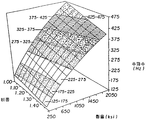
데이터 저장 매체는 부분 혹은 전체적으로 플라스틱 물질(plastic material)을 포함한다. 이 저장 매체는 높은 면적당 기억 용량의 응용들, 데이터 저장층에 입사하는 에너지장이 기판네 접촉함이 없거나 적어도 기판에 접촉하기에 앞서 데이터 저장층에 접촉하는 제 1 표면 및 유사한 응용들이 유용하다. 바꾸어 말하면, 종래의 콤팩트디스크(CD)들과 그와 유사한 응용들과는 현저하게 다르게, 에너지장이 데이터 저장층에 접촉하기 위해 기판을 통하지 않거나, 기판을 통해 반사되어 판독 장치에 돌아온다. 이러한 높은 면적 당 기억용량 응용들에서 기능을 하기 위해서, 저장 매체의 품질이 종래의 콤팩트 디스크 및 관련 매체들의 품질을 능가해야만 한다. 종래의 콤팩트 디스크들 및 관련 매체들과 비교하여, 저장 매체는, 다른 품질들 가운데서, 환경적이고/거나 회전의 진동으로 여기될 때, 감소한 축 방향 변위, 불규칙이나 결함이 거의 없음에 의해 표시되는 보다 높은 표면 품질 및 보다 낮은 회전 관성 모멘트(약 5.5 slug-in2이나 그 이하가 선호되며, 약 4.5 slug-in2이나 그 이하가 더욱 선호되며, 약 4.0 slung-in2이나 그 이하가 특히 선호됨)를 가져야 한다. 게다가, 저장 매체는, 바람직하게 약 5 Gbits/in2를 초과하는 면적당 밀도, 바람직하기로는 약 6 Gbits/in2 이상, 보다 바람직하기로는 약 10 Gbits/in2 이상, 보다 바람직하기로는 약 20 Gbits/in2 이상, 보다 바람직하기로는 약 25 Gbits/in2 이상, 보다 바람직하기로는 약 50 Gbits/in2 이상, 및 약 100 Gbits/in2 까지 이거나 그 이상이 예견된다.The data storage medium comprises a plastic material in part or in whole. This storage medium is useful for applications of high storage capacity per area, first surface contacting the data storage layer before the energy field incident on the data storage layer or at least prior to contacting the substrate and similar applications. In other words, unlike conventional compact discs (CDs) and similar applications, the energy field does not pass through the substrate or is reflected through the substrate to return to the reading device to contact the data storage layer. In order to function in such high per-area storage applications, the quality of the storage medium must outperform the quality of conventional compact discs and related media. Compared with conventional compact discs and associated media, the storage medium is more marked by reduced axial displacement, less irregularities or defects when excited with environmental and / or rotational vibrations, among other qualities. High surface quality and lower rotational moment of inertia (about 5.5 slug-in 2 or less is preferred, about 4.5 slug-in 2 or less is preferred, and about 4.0 slung-in 2 or less is particularly preferred Must have In addition, the storage medium preferably has a density per area exceeding about 5 Gbits / in 2 , preferably at least about 6 Gbits / in 2 , more preferably at least about 10 Gbits / in 2 , and more preferably about 20 Gbits. / in 2 or greater, more preferably about 25 Gbits / in 2 or greater, more preferably about 50 Gbits / in 2 or greater, and up to about 100 Gbits / in 2 or greater.
일반적으로, 높은 면적 당 기억 용량의 응용들, 즉 약 5 Gbits/in2 혹은 그 이상에서, 판독/기록 장치는 상대적으로 저장 매체의 표면에 가깝게 있게 된다(스탠드-오프거리(stand-off distance)). 일반적으로, 높은 용량이 추구되면 될수록 그 만큼 판독/기록 장치는 저장 매체의 표면에 가깝게 있어야 한다. 전형적으로 이러한 실례들에서, 스탠드-오프 거리는 일반적으로 약 0.3 밀리미터(mm) 이하이며, 종종 약 760 나노미터(nm) 이하이다. 고도로 높은 저장 용량을 위해, 판독/기록 장치는 바람직하게 극도로 가까운, 예를 들면, 표면으로부터 약 0.064 미크론(μ) 이하이고, 종종 약 0,013 μ이하이다. 결과적으로 기판의 축 방향 변위는, 진동 및/또는 충격의 상황들 동안에 판독/기록 장치 및/또는 저장 매체의 표면에 손상을 입히지 않도록 하기 위해, 허용 가능한 시스템 편향 거리(deflection distance)보다 훨씬 작아야 한다. 예를 들면, 약 1G의 사인곡선의 중력의 부하를 겪은 디스크(외부 직경이 130mm이고, 내부 직경이 40mm이고, 두께가 1.2mm)에서, 약 170Hz의 공명주파수와, 약 0.051μ의 스탠드-오프 거리, 피크-피크 측정에서 약 250μ이하, 바람직하기로는 150 μ 이하의 축 방향 변위가 선호되며, 기판 및/또는 판독/기록 장치의 손상이 주요 관심일 때, 실례들에서 약 125μ이하가 특히 선호된다. 바람직하게, 피크-피크 측정에서 약 500μ혹은 그 이하의 축 방향 변위(약 250μ나 그 이하가 선호되는)가, 약 2msec에서 약 10msec까지의 응용시간에 약 25G의 최대 충격에서 유지되며, 약 35G에 대해 이러한 변위를 유지하는 것이 선호된다. 그러나, 다른 실례들에서, 예를 들면, 헤드를 손상시키는 더 큰 스탠드-오프 거리(예를 들면, 약 0.30μ나 그 이상의 스탠드-오프)를 갖는 것들은 우세한 논점이 아니며, 차라리 매우 낮은 축 방향 변위 및/또는 디스크 경사가 초점 거리에서 빠른 변화들에 대한 응답이 불가능할 수도 있으므로, 초점을 유지하도록 광학을 고려하는 것이 선호된다. 최대 방사상의 기울기와 접선의 기울기는 독립적이며, 정지 상태에서 측정하여(즉, 회전하지 않는 상태), 약 1°미만, 바람직하기로는 각각이 단지 1°를 초과하지 않거나, 보다 바람직 하기로는 각각이 약 0.3°미만이다.In general, in applications with high storage capacity per area, i.e., about 5 Gbits / in 2 or more, the read / write device will be relatively close to the surface of the storage medium (stand-off distance). ). In general, the higher capacity is to be sought, the closer the read / write device should be to the surface of the storage medium. Typically in these examples, the stand-off distance is generally less than about 0.3 millimeters (mm) and often less than about 760 nanometers (nm). For highly high storage capacities, the read / write device is preferably extremely close, for example, about 0.064 microns (μ) or less from the surface, often about 0,013 μs or less. As a result, the axial displacement of the substrate should be much smaller than the allowable system deflection distance in order to avoid damaging the surface of the read / write device and / or storage medium during vibration and / or shock situations. . For example, at a disk subjected to a gravity load of about 1 G sinusoid (outer diameter 130 mm,
기판의 축 방향 변위는, 디스크 크기의 필요 조건들(내부와 외부의 반경 및 두께), 강성(휨율(flexural modulus))과 밀도, 푸아송 비율(poisson's ratio), 손실률과 저장률, 그리고 이러한 것들과 다른 것들의 결합들을 포함하는 몇 가지 특성들의 함수이지만 이에 국한되지는 않는다. 디스크의 외부의 반경이 증가함에 따라, 충격과 진동의 상황 하에서 디스크의 축 방향 변위 또한 증가하며, 디스크의 두께가 감소함에 따라, 섹션의 강성(sectional stiffness)이 감소하는 한편 축 방향 변위는 증가한다. 현재, 저장 매체의 용적은 현재 이용할 수 있는 저장 매체 판독/기록 장치들에서 사용될 수 있도록 산업에 의해 지정되어 있다. 결과적으로, 저장 매체는 전형적으로 약 40mm에 이르는 내부 직경과, 약 130mm에 이르는 혹은 그 이상의 외부 직경을 가지며, 약 15mm에서 약 40mm까지의 내부 직경과 약 65mm에서 약 130mm까지의 외부 직경이 일반적으로 사용된다. 전형적으로 사용되는 전체적인 두께는 약 0.8mm에서 약 2.5mm까지이며, 전형적으로 약 1.2mm까지의 두께가 선호된다. 원하는 구조를 얻기 위해 다른 직경들과 두께들이 사용될 수 있다.The axial displacement of the substrate is dependent on the disc size requirements (inside and outside radius and thickness), stiffness (flexural modulus) and density, poisson's ratio, loss rate and storage rate, and these It is a function of some features, including but not limited to combinations of and. As the outer radius of the disc increases, the axial displacement of the disc also increases under shock and vibration conditions, and as the thickness of the disc decreases, the sectional stiffness decreases while the axial displacement increases. . Currently, the volume of storage media is specified by the industry to be used in currently available storage media read / write devices. As a result, storage media typically have an inner diameter of about 40 mm and an outer diameter of about 130 mm or more, with an inner diameter of about 15 mm to about 40 mm and an outer diameter of about 65 mm to about 130 mm generally. Used. Typically the overall thickness used is from about 0.8 mm to about 2.5 mm, and typically a thickness up to about 1.2 mm is preferred. Other diameters and thicknesses can be used to obtain the desired structure.
축 방향 변위 외에 또, 강성이 기판의 진동에 대한 기본 주파수에 영향을 미친다. 기본 모드 주파수의 발생이, 물질 특성들 예를 들면, 기판의 휨율, 두께와/나 비중(S.G.)/밀도, 혹은 디자인 구조 예를 들면, 내부/외부의 보강제들을 포함하는 몇 가지 요소들에 입각하여 조정될 수 있다고 결정되었다(도 4를 참조하기 바란다). 모드 주파수들이 기판이 자연적으로 공명하고, 디스크를 평면(plane)의 밖으로 옮겨 놓는 주파수를 규정하므로, 저장 매체의 정규의 동작 주파수의 외부에 기판의 제 1 모드 주파수를 갖는 것이 선호된다. 정규의 동작 주파수는 전형적으로 약 20Hz에서 약 500Hz이며, 미래의 응용들에서는 500Hz 이상이 예견된다. 결과적으로, 제 1 모드 주파수를 저장 매체의 동작 주파수의 외부에 두는 휨율/밀도를 바람직하게 지닌다. 도 4(그 특성들이 다음의 테이블에 도시된)에서 명백한 바와 같이, 휨율과 비중/밀도의 상호관계성이 원하는 휨율과 밀도에 크게 영향을 끼친다. 바람직하게, 강성이 높고 밀도가 낮아야 한다. 전형적으로, 휨율은 약 250kspi(thousand pounds per square inch)이상, 바람직하기로는 약 350kspi(thousand pounds per square inch)이상, 보다 바람직하기로는 약 500kspi 이상, 보다 바람직하기로는 약 1,000kspi이어야 하며, 비중은 바람직하게 약 1.5나 그 이하이며, 약 1.3이나 그 이하가 더욱 선호되고, 약 1.0이나 그 이하의 특정 비중이 특히 선호된다. In addition to axial displacement, stiffness also affects the fundamental frequency of vibration of the substrate. The generation of the fundamental mode frequency is based on several factors including material properties such as substrate warpage, thickness and / or specific gravity (SG) / density, or design structure such as internal / external reinforcements. It can be determined that it can be adjusted (see Fig. 4). Since the mode frequencies define the frequency at which the substrate naturally resonates and moves the disk out of the plane, it is preferred to have the first mode frequency of the substrate outside of the normal operating frequency of the storage medium. The normal operating frequency is typically about 20 Hz to about 500 Hz, with more than 500 Hz expected for future applications. As a result, it preferably has a deflection rate / density that places the first mode frequency outside the operating frequency of the storage medium. As is apparent from FIG. 4 (the characteristics of which are shown in the following table), the correlation between the warpage rate and specific gravity / density greatly influences the desired warpage rate and density. Preferably, it should be high in stiffness and low in density. Typically, the warpage rate should be at least about 250 kspi (thousand pounds per square inch), preferably at least about 350 kspi (thousand pounds per square inch), more preferably at least about 500 kspi, more preferably at least about 1,000 kspi, with specific gravity being Preferably about 1.5 or less, about 1.3 or less is more preferred, and a particular specific gravity of about 1.0 or less is particularly preferred.
사용되는 작은 스탠드-오프 거리와 반송파 대 잡음 비율에서 표면 거칠기(surface roughness)의 악 영향에 기인하여 축 방향 변위를 가지므로, 기판은 높은 표면 품질 특히, 데이터가 저장되는 저장영역에서 높은 표면 품질을 가져야 하며, 대체로 판독/기록 장치나 저장 매체의 표면에 손상을 억제하고, 정확한 데이터의 저장(deposit)과 검색(retrieval)이 가능하도록 대체로 평평해야 한다. 바람직하게, 기판은 적어도 약 100 옹스트롬(Å) 이하의 평균 표면 거칠기(원자력 현미경 검사로 측정되는,(Ra))를 갖는 표면의 부분을 가져야 하며, 약 10Å 이하의 거칠기가 선호되며, 약 5Å 이하의 거칠기가 더욱 선호된다(거칠기는 전형적으로 기판의 10μ×10μ면적의 평균이다). 전형적으로 1mm ×1mm의 면적의 평균인, 표면의 마이크로파는 약 100Å까지 일 수 있으며, 약 10Å까지가 선호되며, 약 5Å까지가 특히 선호된다. 평면도(flatness)("런-아웃(run-out)으로 알려진)에 대하여, 실질적으로 융기된 부분들이나 골들이 없는 평평한 기판이 특히 선호된다. 약 100μ까지의 런-아웃이 사용 될 수 있고, 약 10μ까지의 런-아웃이 선호되며, 약 5μ까지의 런-아웃이 특히 선호된다(평면도는 전형적으로 전체 디스크 영역의 평균이다).Since the substrate has axial displacement due to the small stand-off distance used and the adverse effect of surface roughness on the carrier-to-noise ratio, the substrate has a high surface quality, especially in the storage area where data is stored. It should be generally flat to prevent damage to the surface of the read / write device or storage medium and to allow for the accurate storage and retrieval of data. Preferably, the substrate should have a portion of the surface having an average surface roughness (R a , as measured by atomic force microscopy) of at least about 100 Angstroms, with a roughness of about 10 GPa or less preferred, and about 5 GPa The following roughness is more preferred (roughness is typically the average of 10 μ × 10 μ area of the substrate). Microwaves on the surface, typically averaged over an area of 1 mm x 1 mm, can be up to about 100 mW, with up to about 10 mW preferred, and up to about 5 mW particularly preferred. For flatness (known as " run-out "), flat substrates that are substantially free of raised portions or valleys are particularly preferred. Runouts of up to about 100 microns can be used, and Run-outs of up to 10 microns are preferred, and run-outs of up to about 5 microns are particularly preferred (top views are typically the average of the entire disk area).
이러한 작은 스탠드-오프 거리들에서, 보통 에지-리프트(edge-lift)나 스카이-점프(ski-jump)로 알려진, 기판의 가장자리나 그 근처의 융기는 판독/기록 장치에 손상을 일을 킬 수 있다. 기판은 약 8μ이하의 에지-리프트 높이를 가져야 하며, 약 5μ이하가 선호되며, 약 3μ이하가 특히 선호되며, 약 800μ이하의 에지-리프트 길이가 선호되며, 약 500μ이하의 에지-리프트 길이가 특히 선호된다.At these small stand-off distances, ridges at or near the substrate, commonly known as edge-lift or ski-jump, can damage the read / write device. have. The substrate should have an edge-lift height of less than about 8μ, less than about 5μ is preferred, less than about 3μ is particularly preferred, an edge-lift length of less than about 800μ is preferred, and an edge-lift length of less than about 500μ Especially preferred.
저장 매체는 다양한 시스템에서 사용될 수 있으며, 그 중의 일부가 기판의 강성 붕괴를 고려할 필요가 있는 억제 장치를 사용할 것이다. 저장 매체를 보호하기 위해 클램프(clamp), 허브(hub), 혹은 다른 억제 장치를 사용하는 판독/기록 장치에 있어서, 기판은 기계적 붕괴(시간과/이나 온도 양자에 입각한)를 피하기에 층분한 항복 스트레스(yield stress)를 가져야 한다. 약 65mm에서 약 130mm의 외부 직경을 갖는, 판독/기록 시스템의 억제 장치 내에서 보호 될 저장 매체에서, 사용되는 플라스틱 수지들은 약 7000 psi나 그 이상의 항복 스트레스가 선호되며, 약 9,000psi를 넘는 항복 스트레스가 특히 선호된다. 충진 엔지니어링(filled engineering) 플라스틱 수지들의 경우에, 더욱 높은 항복 스트레스를 얻을 수 있으며, 평방 인치 당(psi) 약 10,000 파운드(pound)를 넘는 항복 스트레스가 선호되며, 약 15,000psi 이상이 특히 선호된다.Storage media can be used in a variety of systems, some of which will use suppression devices that need to account for rigid collapse of the substrate. In read / write devices that use clamps, hubs, or other restraint devices to protect the storage medium, the substrate may be difficult to avoid mechanical decay (both time and / or temperature). You must have yield stress. In storage media to be protected within the suppression device of the read / write system, having an outer diameter of about 65 mm to about 130 mm, the plastic resins used are preferably yield stresses of about 7000 psi or more, and yield stresses above about 9,000 psi. Is particularly preferred. In the case of filled engineering plastic resins, higher yield stresses can be achieved, yield stresses of greater than about 10,000 pounds per square inch are preferred, and greater than about 15,000 psi are particularly preferred.
몇 가지의 이러한 디스크들은 도 25에서 도 27까지 설명된다. 도 25는 중합체 표면(202), 충진되거나 빈 코어(a filled or hollow core)(204), 금속(예를 들면, 알루미늄), 유리, 세라믹, 금속-매트릭스 합성물(metal-matrix composit), 및 이러한 것들 중의 적어도 하나를 포함하는 합금과 결합들, 기타 등등과 같은, 플라스틱(202)보다 높은 항복 스트레스를 포함하는 물질의 중심부(206)를 갖는 디스크(200)를 도시한다. 도 26은 클램프(208)에 부착된 높은 항복 스트레스 중심 부분(206)을 갖는다. 한편, 도 27은 중합체가 중심부(206)와 같은 물질로 이루어진 코어(204) 위에 있는 얇은 필름(thin film)인 다른 실시예를 설명한다. 예를 들면, 코어는 코어의 전부 혹은 일부분의 위에 배치된 플라스틱 필름(202)을 갖는 금속일 수 있다. Some such disks are described in FIGS. 25 through 27. 25 shows a
종래의 기판들 예를 들면, 플라스틱 도금이 없는 알루미늄과 세라믹 기판들은 아주 높은 강성(예를 들면, 약 70 기가파스칼(GPa)의 영률(Young's modulus)을 갖는 알루미늄과 약 200GPa의 영률을 갖는 세라믹)을 가지며, 이러한 레벨들은 플라스틱 기판들로 인해 달성되었다. 뜻밖에, 물질의 감쇠 계수가 알루미늄과 비교하여 플라스틱 기판들의 감소된 강성을 벌충하는 데에 중요하다는 것이 발견되었다. 결과적으로, 디스크의 진동의 영향을 최소화하기 위해, 기판의 점성과 탄성을 지닌 물질의 특성들이 감쇠 성능을 가능하게 하도록 조정될 수 있다. 예를 들면, 진동 원(vibration source)과 진동되는 물체 사이에 적절한 스프링/대시포트 어셈블리(spring/dashport assembly)을 삽입함에 의해, 진동 감쇠는 일반적인 정도로 이루어진다. 효과적인 감쇠를 위해, 물질은 플레이너 쉬어링(planar shearing)이나 물질의 부피 압축(bulk compression)과 팽창의 결과로서 전환되는 에너지(예를 들면, 열 에너지)로서 물질을 통해 전달되는 진동의 에너지를 흡수 및/또는 방산해야 한다.Conventional substrates, such as aluminum and ceramic substrates without plastic plating, have very high stiffness (for example, aluminum having a Young's modulus of about 70 gigapascals (GPa) and ceramic having a Young's modulus of about 200 GPa) These levels were achieved due to the plastic substrates. Unexpectedly, it has been found that the damping coefficient of the material is important for compensating for the reduced stiffness of plastic substrates compared to aluminum. As a result, in order to minimize the influence of vibration of the disk, the properties of the viscous and elastic material of the substrate can be adjusted to enable the damping performance. For example, by inserting a suitable spring / dashport assembly between the vibration source and the vibrating object, vibration damping is achieved to a general degree. For effective damping, the material absorbs the energy of the vibrations transmitted through the material as energy (eg, thermal energy) that is converted as a result of planar shearing or bulk compression and expansion of the material. It must be absorbed and / or dissipated.
플라스틱 수지들과 같은 점성과 탄성을 지닌 물질들에는 저장률과 손실률 양자가 존재한다. 저장률은 탄성 강성을 나타내고 손실률은 점성 강성을 나타낸다. 알루미늄보다 낮은 강성을 갖는 저장 매체에서, 기판이 75°F(약 24°C)의 온도에서 약 0.04 이상, 바람직하기로는 약 0.05 이상, 보다 바람직하기로는 약 0.06이상의 기계적 감쇠 계수(저장률에 대한 손실률의 비율로 정의되는)를 갖는 것이 선호되며, 75°F의 온도에서 약 0.10 이상의 기계적 감쇠 계수를 갖는 것이 선호되며, 75°F의 온도에서 약 0.15 이상의 기계적 감쇠 계수를 갖는 것이 특히 선호된다.Both viscous and elastic materials such as plastic resins have both storage and loss rates. The storage rate indicates elastic stiffness and the loss rate indicates viscous stiffness. In storage media with lower stiffness than aluminum, the substrate has a mechanical attenuation coefficient of at least about 0.04, preferably at least about 0.05 and more preferably at least about 0.06 at a temperature of 75 ° F (about 24 ° C.) Preference is given to having a mechanical attenuation coefficient of at least about 0.10 at a temperature of 75 ° F, and particularly preferred to a mechanical attenuation coefficient of at least about 0.15 at a temperature of 75 ° F.
게다가, 물질의 감쇠 특성들은, 주파수와 온도의 관련 범위에서, 감쇠 계수가 원하는 값 밑으로 떨어지지 않을 정도로, 최적화될 수 있다. 몇 가지의 실시예에서, 관련 온도 범위와 감쇠의 응용성을 위한 주파수 범위는 약 75°F(24°C)와 약 2Hz에서 약 150°F(65.5°C)와 약 400Hz가 선호되며, 약 32°F(0°C)와 약 2Hz에서 약 200°F(93.3°C)와 약 500Hz가 더욱 선호된다.In addition, the damping properties of the material can be optimized so that the damping coefficient does not fall below the desired value in the relevant range of frequency and temperature. In some embodiments, the frequency range for the application of the relevant temperature range and attenuation is preferably about 75 ° F (24 ° C) and about 2 Hz at about 150 ° F (65.5 ° C) and about 400 Hz. More preferred are about 200 ° F (93.3 ° C) and about 500Hz at 32 ° F (0 ° C) and about 2Hz.
도 5와 도 7은 다양한 물질 특성들에 대한 1G 사인곡선의 진동의 부하에 대한 축 방향 변위와 고정된 기하학들 사이의 관계를 나타낸다. 도 6은 감쇠 계수가 제 1 모드 주파수에 영향을 끼치지 않으며, 반면 도 7은 제 1 모드 주파수에서 축 방향 변위의 영향을 보여준다.5 and 7 show the relationship between axial displacement and fixed geometries for a load of vibration of a 1G sinusoid for various material properties. FIG. 6 shows that the damping coefficient does not affect the first mode frequency, while FIG. 7 shows the effect of axial displacement at the first mode frequency.

감쇠(또한 dampening으로도 언급됨)는 에너지 흡수 성분의 부가와 같은 다양한 접근을 통해서나 다양한 필터들과 보강제(reinforcing agents)들을 포함하는 슬립 장치들(slip mechanisms)을 통해 이루어질 수 있다. 감쇠 특성들을 개선할 수 있는 유용한 물질들은, 가황 고무(vulcanized rubbers), 아크릴 고무(acrylic rubbers), 실리콘 고무(silicone rubbers), 부타디엔 고무(butadiene rubbers), 이소부틸렌 고무(isobutylene rubbers), 폴리에스테르 고부(polyether rubbers), 이소부틸렌-이소프렌 중합체와 이소시아네이트 고무(isobutylene-isoprene copolymers and isocyanate rubber), 니트릴 고무(nitrile rubbers), 클로로프렌 고무(chloroprene rubbers), 클로로슬폰 폴리에틸렌(chlorosulfonated polyethylene), 폴리설파이드 고무(polysulfide rubbers)와 플루오르 고무(fluorine rubber), 미국 특허 제 4,987,194호(본 명세서에 참조 인용한)에 개시된 바와 같은 폴리스티렌-폴리이소프렌(polystyrene-polyisoprene) 공중합체들을 포함하는 블록 공중합체(block copolymers), 열가소성의 엘라스토머 물질(thermoplastic elastomer materials), 폴리우레탄(polyurethanes)을 포함하는, 그리고 특히 이러한 것들 중에 적어도 하나를 포함하는 화합물들과 같은, 높은 감쇠 성능(예를 들면, 약 0.05 이상의 감쇠 계수)을 갖는 탄성 물질들을 포함한다. 진동 감쇠 물질들은 또한, 다량의 입자들(particles)(페라이트, 금속, 세라믹 및 같은 종류의 것들), 박편들(flakes)(활석, 운모 및 같은 종류의 것들), 다양한 섬유(산화아연, 규회석, 탄소섬유, 유리섬유 및 같은 종류의 것들) 그리고 이러한 것들 중 적어도 하나를 포함하는 혼합물들(mixtures)이 사용될 수 있는, 수지들을 포함한다. 마이크로섬유들(microfibers), 미소섬유들(fibrils), 나노튜브들(nanotubes), 수염들(whiskers), 거품(foamed)과 벌집(honeycombed)의 구조들이 이러한 것들의 다양한 결합으로서 또한 유용할 수도 있다.Damping (also referred to as dampening) can be accomplished through various approaches, such as the addition of energy absorbing components, or through slip mechanisms including various filters and reinforcing agents. Useful materials that can improve damping properties include vulcanized rubbers, acrylic rubbers, silicone rubbers, butadiene rubbers, isobutylene rubbers, polyesters Polyether rubbers, isobutylene-isoprene copolymers and isocyanate rubbers, nitrile rubbers, chloroprene rubbers, chlorosulfonated polyethylene, polysulfide rubbers block copolymers comprising polystyrene-polyisoprene copolymers as disclosed in polysulfide rubbers and fluorine rubber, US Pat. No. 4,987,194 (incorporated herein by reference). , Thermoplastic elastomeric materials, polyurethanes To, and includes a resilient material having in particular at least one, and high damping performance, such as a compound comprising (e.g., about 0.05 or more attenuation coefficients) in these. Vibration damping materials can also contain large amounts of particles (ferrites, metals, ceramics and the like), flakes (talcum, mica and the like), various fibers (zinc oxide, wollastonite, Carbon fibers, glass fibers and the same kind) and mixtures comprising at least one of these may be used. The structures of microfibers, fibrils, nanotubes, whiskers, foamed and honeycombed may also be useful as various combinations of these. .
기판에서 감쇠 물질들의 사용을 통해 축 방향 변위를 줄이는 것 외에, 혹은 대신에, 기판을 지탱하는 억제 장치나 클램핑 구조에 진동 감쇠 물질을 이용함에 의해 축 방향 변위가 줄어들 수 있다. 클램프나 클램프와 기판의 사이에 점성과 탄성을 지닌 물질들의 부가는 부가물이 없는 동일한 구조와 비교하여 디스크의 축 방향 변위를 효과적으로 줄인다. 하나의 실시예에서, 진동-감쇠 물질은 바람직하게 디스크 기판의 감쇠 계수보다 높은 감쇠 계수와 크리프(creep) 특성을 줄이기에 층분히 높은 탄성률, 예를 들면, 20 kpsi보다 큰 탄성률을 가져야 한다. 클램프의 댐핌 특성들을 개선할 수 있는 유용한 물질들은, 가황 고무, 아크릴 고무, 실리콘 고무, 부타디엔 고무, 이소부틸렌 고무, 폴리에스테르 고무, 이소부틸렌-이소프렌 중합체와 이소시아네이트 고무, 니트릴 고무, 클로로프렌 고무, 클로로슬폰화 폴리에틸렌, 폴리설파이드 고무와 플루오르 고무, 미국 특허 제 4,987,194호에 개시된 바와 같은 폴리스티렌-폴리이소프렌 공중합체들을 포함하는 블록 공중합체, 열가소성의 엘라스토머 물질, 폴리우레탄을 포함하는, 그리고 특히 이러한 것들의 화합물들과 같은, 높은 탬핑 능력을 갖는 탄성 물질들을 포함한다. 거품이나 벌집의 구조들이 또한 유용할 수 있다.In addition to or instead of reducing the axial displacement through the use of damping materials in the substrate, the axial displacement can be reduced by using vibration damping materials in the suppressor or clamping structure supporting the substrate. The addition of a viscous and elastic material between the clamp or the clamp and the substrate effectively reduces the axial displacement of the disk compared to the same structure without any additives. In one embodiment, the vibration-damping material should preferably have an elastic modulus that is significantly higher than the damping coefficient of the disk substrate and that is significantly higher in order to reduce creep properties. Useful materials that can improve the damping properties of the clamp include vulcanized rubber, acrylic rubber, silicone rubber, butadiene rubber, isobutylene rubber, polyester rubber, isobutylene-isoprene polymer and isocyanate rubber, nitrile rubber, chloroprene rubber, Chlorosulfonated polyethylene, polysulfide rubber and fluorine rubber, block copolymers including polystyrene-polyisoprene copolymers as disclosed in US Pat. No. 4,987,194, thermoplastic elastomeric materials, including polyurethanes, and in particular of these Elastic materials having high tamping capabilities, such as compounds. Bubble or honeycomb structures may also be useful.
저장 매체의 안정성과 수명에 영향을 끼치는 다른 요소들은 용적의 안정성(dimensional stabilities)과 열수 작용의 특성(hygrothermal properties)과 관련이 있다. 저장 매체의 저장과 작동 온도 범위 내의 온도에서 열과 습기의 용적의 안정성을 갖는 기판은 전형적으로 용인할 수 있는 약 -6°C(21°F)에서 약 40°C(104°F)의 온도에서 열과 습도의 안정성으로 사용될 수 있으며, -12°C(10°F)에서 약 80°C(175°F)의 온도 내에서의 안정성이 선호되며, 약 -16 °C(3°F)에서 약 100°C(212°F)의 온도에서의 안정성이 특히 선호된다. 저장 매체가 사용되고 보관될 수 있는 변화하는 환경들에 기인하여, 저장 매체는 바람직하게 다음을 갖는다: (1)약 60°C(140°F) 이상의 열 의곡 온도(약 80°C 이상이 선호됨); (2)바람직하게 비스페놀-A 기반의 폴리카보네이트 수지( bisphenol-A based polycarbonate)와 같거나 그 이상인 크리프 특성; (3)기판이 구부러짐(bow)이나 뒤틀림(warp)과 같이 상당히 모양이 변하지 않는 정도로 좋은 습도-온도 특성. 85%의 상대 습도에서 80°C의 테스트 상황 하에서 4주 후에, 평형상태에서, 바람직하게, 기판의 습기 함유량이 약 1.0% 이하로 변하며, 평형상태에서 약 0.5% 이하가 더욱 선호되며, 평형상태에서 약 0.3% 이하가 특히 선호된다.Other factors affecting the stability and longevity of storage media are related to dimensional stabilities and hygrothermal properties. Substrates that have stability in volume of heat and moisture at temperatures within the storage and operating temperature range of storage media are typically acceptable at temperatures from about -6 ° C (21 ° F) to about 40 ° C (104 ° F). It can be used for stability of heat and humidity, and stability at temperatures of -12 ° C (10 ° F) to about 80 ° C (175 ° F) is preferred, and at -16 ° C (3 ° F) Stability at temperatures of 100 ° C. (212 ° F.) is particularly preferred. Due to the changing circumstances in which the storage medium can be used and stored, the storage medium preferably has: (1) a thermal grain temperature of about 60 ° C. (140 ° F) or more (preferably about 80 ° C. or more). ); (2) creep properties, preferably equal to or greater than bisphenol-A based polycarbonate; (3) Humidity-temperature characteristics that are good enough that the substrate does not change shape considerably, such as bow or warp. After 4 weeks under test conditions of 80 ° C. at 85% relative humidity, at equilibrium, the moisture content of the substrate preferably changes to about 1.0% or less, with less than about 0.5% preferred at equilibrium, Less than about 0.3% is particularly preferred.
전술한 디자인 문제들을 해결하기 위해, 이러한 기판은 동질의 것이나 이질의 것일 수 있으며, 다수의 기하학을 가질 수 잇다. 동질의 기판은 대체로 고체인 플라스틱일 수 있으며, 혹은 가변 다공성 혹은 하나 이상의 공동(cavities)을 포함할 수도 있다(도 15, 도 16, 도 17 및 도 33에서 도 35를 참조하기 바란다). 이러한 도면들에서 도시된 바와 같이, 기판의 밀도는 기판 내에 하나 이상의 속이 빈 공동(구멍, 거품들, 통로, 거미집 모양, 등등)을 사용하는 한편, 데이터가 저장될 저장 매체의 영역에서 기판 내에 공동을 포함함에 의해서나 기판 위에 코팅을 사용함에 의해서 층분히 매끄러운 표면을 유지함에 의해 줄어들 수 있다.To solve the aforementioned design problems, these substrates can be homogeneous or heterogeneous and can have multiple geometries. The homogeneous substrate may be a generally solid plastic or may comprise variable porosity or one or more cavities (see FIGS. 15, 16, 17 and 33, see FIG. 35). As shown in these figures, the density of the substrate uses one or more hollow cavities (holes, bubbles, passages, cobwebs, etc.) within the substrate, while cavities within the substrate in the area of the storage medium on which data is to be stored. It can be reduced by maintaining a smooth surface, by including or by using a coating on the substrate.
공동들의 크기, 모양 및 위치는 상기에 언급한 디자인 표준들에 입각한다. 예를 들면, 도 17에서, 공동들은 기판의 외부 직경 근처에 위치될 수 있으며, 판독/기록 시스템의 허브에서 안정할 수 있는 기판의 중심 영역이 기판의 외부의 둘레가 줄어든 밀도와 관성 논점들을 갖는 반면 최대의 항복 강도를 갖도록 한다. 도 8에서 도 14, 도 33에서 도 35에 도시된 바와 같이, 공동이 다양한 기하학(선형, 곡선, 볼록(convex), 오목(concave), 볼록-오목(convex-concave), 오목-오목(concave-concave), 볼록-볼록(convex-convex) 및 그와 같은 것들), 크기(폭, 길이, 높이), 기판 도처에 위치들(내부 직경에서 외부 직경가지 때때로 중단되는 혹은 그들 사이의 어떤 위치)을 가질 수 있고, 서로 연결시키거나 분리할 수 있다.The size, shape and location of the cavities is based on the design standards mentioned above. For example, in FIG. 17, the cavities can be located near the outer diameter of the substrate and the central region of the substrate, which can be stable at the hub of the read / write system, has density and inertia issues with reduced perimeter of the outside of the substrate. On the other hand, it has the maximum yield strength. As shown in FIGS. 8 to 14 and 33 to 35, the cavity has various geometries (linear, curved, convex, concave, convex-concave, concave-concave). -concave, convex-convex and the like), size (width, length, height), locations throughout the substrate (sometimes the outer diameter to the inner diameter is interrupted or between them) And may be connected to or separated from each other.
이질의 기판은 충진제, 코어, 혹은 다른 보강제나 삽입물을 갖는 플라스틱일 수 있으며, 혹은 이러한 것들의 혼합이나 화합 물질일 수도 있다(도 8에서 도 27을 참조하기 바란다). 다양한 도면들에서 도시되고, 더욱 상세히 후술하는 바와 같이, 삽입물/ 코어/보강제의 물질 기하학, 위치 및 크기는 상호 연결이나 분리, 고체나 비-고체, 평판, 거미줄 디자인, 허브 디자인, 보강 구조, 내부 직경과/이나 외부 직경 삽입물, 상면, 중간, 바닥, 혹은 오프셋 디자인들, 손가락 모양 혹은 방향성 디자인, 동심원(concentric) 보강제, 부분적 표면, 용접된(welded), 접착된(bonded), 혹은 캡슐에 싸인(encapsulated) 디자인; 혹은 이러한 것들 중의 적어도 하나를 포함하는 결합과 같은 다양한 디자인 범주를 해결하기 위해 조절될 수 있다.The heterogeneous substrate may be a filler, a core, or a plastic with other reinforcements or inserts, or may be a mixture or compound of these (see FIGS. 8 to 27). As shown in the various figures and described in more detail below, the material geometry, location, and size of the insert / core / reinforcement may be interconnected or separated, solid or non-solid, plate, cobweb design, hub design, reinforcement structure, interior Diameter and / or outer diameter inserts, top, middle, bottom, or offset designs, finger or directional designs, concentric reinforcements, partial surfaces, welded, bonded, or encapsulated (encapsulated) design; Or can be adjusted to address various design categories, such as combinations involving at least one of these.
도 22에서 도 24를 참조하면, 예를 들어 기판이, 실질적으로 기판의 용적 전부를 포함하며, 대부분의 플라스틱이 단지 기판의 표면 가까이에 예를 들면, 얇은 필름으로 배치되는 보강제를 가질 수 있다. 이러한 실시예에서, 대부분의 기판을 형성하는 코어는 약 2.5mm 까지의 두께를 가질 수 있으며, 약 0.75mm에서 약 2.0mm의 두께가 선호되며, 약 0.8mm에서 약 1.2mm의 두께가 특히 선호된다. 도시된 바와 같이, 얇은 플라스틱 필름은 코어(예를 들면, 금속, 세라믹, 유리 및 그와 같은 것들)의 한쪽면이나 양쪽면에 배치될 수 있다. 전형적으로, 약 50μ나 그 이하의 두께를 갖는 플라스틱 필름이 사용될 수 있으며, 20μ나 그 이하의 두께가 선호되다.Referring to FIGS. 22 to 24, for example, the substrate may have a reinforcement that comprises substantially all of the volume of the substrate, and most plastics are only disposed in, for example, a thin film near the surface of the substrate. In this embodiment, the core forming most substrates may have a thickness of up to about 2.5 mm, with a thickness of about 0.75 mm to about 2.0 mm being preferred, with a thickness of about 0.8 mm to about 1.2 mm being particularly preferred. . As shown, the thin plastic film may be disposed on one or both sides of the core (eg, metal, ceramic, glass, and the like). Typically, plastic films having a thickness of about 50 microns or less can be used, with a thickness of 20 microns or less preferred.
기판이, 동질이든 이질이든, 비었거나 찬 공동들이거나, 보강제를 포함하거나 상관없이, 코어/삽입물/보강제의 기하학은 물론이고, 이것들의 기하학도 또한 다양한 디자인 요소들을 다루도록 상호교환적으로 조정될 수 있다. 도 8에서 도 35를 참조하면, 다양한 기판과 코어/삽입물 기하학들은 각각, 가변 두께 및 실질적으로 일정한 두께, 한쪽면이나 양쪽 테이퍼 형상, 한쪽면이나 양 쪽이 볼록하거나 오목한, 혹은 이러한 것들 중의 적어도 하나를 포함하는 결합들을 실질적으로 포함한다.Regardless of whether the substrate is homogeneous or heterogeneous, empty or cold cavities, or includes a reinforcement, the geometry of the core / insert / reinforcement, as well as their geometry, can also be interchangeably adjusted to cover various design elements. have. 8 to 35, the various substrate and core / insert geometries are of varying thickness and substantially constant thickness, one or both tapered shapes, one or both convex or concave, or at least one of these. Substantially includes combinations including.
기판의 기하학은 회전할 때 기판의 관성 모멘트의 조작과 모드 응답 즉, 그것의 고조파(harmonics)의 제어를 가능하게 한다. 예를 들면, 다양한 모드 형태(도 36에서 보이는 바와 같이)가 평면과/이나 방사상의 두께를 통한 밀도에서 부분적인 변화에 입각하여 얻어질 수 있고 피할 수도 있다. 위에서 말한 바와 같이, 선호되는 디자인은 저장 매체가 디자인되는 주파수 영역의 외부의 제1 모드 공명 주파수를 갖는 기판이다.The geometry of the substrate makes it possible to manipulate the moment of inertia of the substrate and the mode response, ie its harmonics, as it rotates. For example, various mode shapes (as shown in FIG. 36) can be obtained and avoided based on partial variations in density through plane and / or radial thickness. As mentioned above, the preferred design is a substrate having a first mode resonance frequency outside of the frequency region in which the storage medium is designed.
저장 매체에 대한 다양한 디자인 표준들을 다루는 다른 방법은, 데이터가 저장되고 검색될 수 있는 속도에 영향을 미치는 작동 회전 속도와 같은, 그 사용법을 다루는 것이다. 종래에는 사용하는 동안에 저장 매체가 일정한 속도로 회전되었다. 매체는 어떤 판독나 기록에 앞서 작동 회전 속도에 도달된다. 그러나, 저장 매체는, 속도가 피크의 사용 주기 동안 증가하는 반면, 보통의 사용 주기 동안 감소하는, 변화하는 속도로 회전될 수 있다; 혹은 회전 속도는 디스크의 다른 영역들(예를 들면, 내부 대 외부 직경)에서 일정한 선형 속도를 유지하기 위하여 변화될 수 있다. 이러한 작동 표준들은 에너지를 일정하게 유지하고, 어쩌면 몇 가지 디자인 표준들을 더욱 중요하게 할 것이다. 이러한 표준들은 예를 들어 관성 모멘트, 계수(modulus), 밀도, 점탄성(viscoelasticity), 두께, 그리고/혹은 직경을 포함한다. 속도를 바꾸는 저장 매체 장치들은 일정한 속도의 장치들에 비교하여 중요성이 증가한 많은 이러한 표준들 예를 들면, 관성 모멘트와 밀도 등등을 만든다. Another way of dealing with various design standards for storage media is to address its usage, such as the operating rotational speed, which affects the speed at which data can be stored and retrieved. Conventionally, the storage medium has been rotated at a constant speed during use. The medium reaches the operating rotational speed prior to any reading or writing. However, the storage medium can be rotated at varying speeds, while the speed increases during the peak usage period, while decreasing during the normal usage period; Alternatively, the rotational speed can be varied to maintain a constant linear speed in other areas of the disc (eg, inner to outer diameter). These operating standards will keep energy constant, and perhaps make some design standards more important. These standards include, for example, moments of inertia, modulus, density, viscoelasticity, thickness, and / or diameter. Speed changing storage media devices create many of these standards, such as moments of inertia and density, etc., of increasing importance compared to devices of constant speed.
이론적으로, 적절한 특성들을 나타내는 플라스틱이 기판, 코어, 그리고/혹은 코팅으로서 사용될 수 있다. 그러나, 플라스틱은 스퍼터링(즉, 자기매체에 대해 약 200°C까지나 초과하는(전형적으로 300°C까지나 초과하는) 온도와 자기-광학 매체에 대해 약 150°C까지의 실온에 대한 온도)과 같은 다음의 처리 파라메타들(예를 들면, 다음의 층들의 적용)을 견딜 수 있어야 한다. 즉, 플라스틱이 증착 단계들 동안 변형을 막기 위해 충분한 열적 안정성을 갖는 것이 바람직하다. 자기 매체에 있어서, 적절한 플라스틱은 적어도 140°C 이상, 바람직하기로는 150°C 이상의 큰유리 천이 온도를 갖는 열가소성 수지를 포함하며, (예를 들어,폴리에테르이미드(polyetherimides),폴리에테르에테르케톤(poletheretherketones), 폴리술폰(polysulfones), 폴리에테르술포(polyethersulfones), 폴리에테르에테르술폰(polyetherethersulfones), 폴리페닐렌에테르( polyphenylene ethers), 폴리이미드(polyimides), 고열 폴리카보네이트(high heat polycarbonates), 등등)것들이 선호되며, 술폰디아닐린(sulfonedianiline)이나 옥시디아닐린(oxidianiline)이 m-페닐렌디아민(m-phenylenediamine)으로 대체되는 폴리에테르이미드와, 폴리이미드는 물론, 프로브이미드(probimide)(혹은 Ciba Geigy Chemical의 드라이 파우더 등가물(dry powder equivalent), Matrimid 5281)와 같은, 약 250°C 이상의 큰 유리 천이 온도를 갖는 물질들이 더욱 선호되며; 이러한 것들 중의 적어도 하나를 포함하는 화합물들 등등을 포함한다.In theory, plastics exhibiting appropriate properties can be used as the substrate, core, and / or coating. However, plastics can be sputtered (ie, temperatures up to about 200 ° C. for magnetic media (typically up to 300 ° C.) and room temperature up to about 150 ° C. for magnetic-optical media). It must be able to withstand the following processing parameters (eg application of the following layers). That is, it is desirable for the plastic to have sufficient thermal stability to prevent deformation during the deposition steps. In magnetic media, suitable plastics include thermoplastics having a large glass transition temperature of at least 140 ° C. or higher, preferably 150 ° C. or higher (eg, polyetherimides, polyetheretherketone ( poletheretherketones, polysulfones, polyethersulfones, polyetherethersulfones, polyphenylene ethers, polyimides, high heat polycarbonates, etc.) Preferred are polyetherimides in which sulfonedianiline or oxidianiline are replaced with m-phenylenediamine, polyimide, as well as probeimide (or Ciba Geigy). More materials with large glass transition temperatures above about 250 ° C., such as chemical dry powder equivalent, Matrimid 5281) Preferred are; Compounds including at least one of these, and the like.
또한, 스탬핑 상황 하에서 층분한 흐름을 갖는 열경화성이 제공되는 응용에서 사용되는 열경화성에 있어서, 원하는 표면 형태들을 형성하도록 하는 것이 가능하다. 다양한 응용들이 다른 유리 천이 온도를 갖는 중합체들을 필요로 할 수도 있으므로, 원하는 유리 천이 온도를 갖는 필름을 얻기 위해, 플라스틱(호모중합체(homopolymers), 공중합체 혹은 블렌드(blend))의 유리 천이 온도를 조정할 수 있도록 하는 것이 유익할 수도 있다. 마지막으로, 미국 특허 제 5,534,602(Lnpinski와 Cole, 1996)에 개시된 바와 같은 중합체 블렌드들이 코딩 솔루션(solution)에 대비하여 사용될 수 있다. 이러한 예에서, 중합체 블렌드들은 약 190°C에서 약 320°C의 가변의 유리 천이 온도를 선택적으로 제공한다.It is also possible to form the desired surface morphologies for thermosetting used in applications where thermosetting with a streamlined flow is provided under a stamping situation. Since various applications may require polymers with different glass transition temperatures, the glass transition temperature of the plastic (homopolymers, copolymers or blends) may be adjusted to obtain a film with the desired glass transition temperature. It may be beneficial to make it possible. Finally, polymer blends as disclosed in US Pat. No. 5,534,602 (Lnpinski and Cole, 1996) can be used in contrast to coding solutions. In this example, the polymer blends optionally provide a glass transition temperature that varies from about 190 ° C. to about 320 ° C.
플라스틱의 몇 가지의 가능한 예들은 무정형(amorphous), 결정형(crystalline) 및 반-결정형 열가소성(semi-crystalline thermoplastic) 물질, 즉 폴리염화비닐(polyvinlyl chloride), 폴리레핀(선형과 고리형의 폴리레핀들을 포함하며, 폴리에틸렌(polyethylene), 염화 폴리에틸렌(chlorinated polyethylene), 폴리프로필렌(polypropylene) 등을 포함하지만, 이에 제한되지는 않는다), 폴리에스테르(폴리에틸렌 테레프탈레이트(polyethylene terephthalate), 폴리부틸렌 테레프탈레이트(polybutylene terephthalate), 폴리시클로헥실메틸렌 테레프탈레이트(polycyclohexylmethylene terephthalate)등을 포함하지만 이에 국한되지는 않는다), 폴리아이드(polyamides), 폴리술폰(수소화 폴리술폰(hydrogenated polysulfones)등을 포함하지만 이에 국한되지는 않는다), 폴리이미드(polyimides), 폴리에테르 이미드, 폴리에테르 술폰, 폴리페닐렌 설파이드(polyphenylene sulfides), 폴리에테르 케톤(polyether ketones), 폴리에테르에테르 케톤(polyetherether ketones), ABS 수지, 폴리스티렌(수소화 폴리스티렌(hydrogenated polystyrenes), 신디오탁틱 및 아탁틱 폴리스티렌(syndiotactic and atactic polystyrenes), 폴리시클로헥실 에틸렌(polycyclohexyl ethylene), 스티렌-코-아크릴로니트릴(styrene-co-acrylonitrile), 스티렌-코-말레 아크릴로니트릴(styrene-co-maleic acrylonitrile)등을 포함하지만 이에 국한되지는 않는다), 폴리부타디엔(polybutadiene), 폴리아크릴레이트)(폴리메틸메타크릴레이트, 메틸 메타크릴레이트 폴리이미드 공중합체(methyl methacrylate-polyimide copolymers)등을 포함하지만 이에 국한되지는 않는다), 폴리아크릴로니트릴(polyacrylonitrile), 폴리아세탈(polyacetals), 폴리카보네이트(polycabonates), 폴리페닐렌 에테르(2,6-디메틸페놀(dimethylphenol)과 2,3,6-트리메틸페놀(trimethylphenol)을 갖는 공중합체에서 얻은 것등을 포함하지만 이에 국한되지는 않는다), 에틸렌-비닐 아세테이트 공중합체(ethylene-vinyl acetate copolymer), 폴리비닐 아세테이트(polyvinly acetate), 리퀴드 크리스탈 중합체(liquid crystal polymers), 에틸렌 테트라플루오르에틸렌 공중합체(ethylene-tetrafluoroethylene copolymer), 방향성 폴리에스테르(aromaticpolyesters), 폴리불화비닐(polyvinly fluoride), 불화비닐리덴 수지(polyvinylidene fluoride), 염화비닐리덴 수지(polyvinylidene chloride), 테프론(Teflons)은 물론 에폭시(epoxy), 페놀릭(phenolic), 알키드수지(alkyds), 폴리에스테르, 폴리이미드, 폴리우레탄, 미네랄 충진 실리콘(mineral filled silicone), 비스-메일이미드(bis-maleimides), 시아네이트 에스테르(cyanate esters), 비닐, 벤조시클로부틴 수지(benzocyclobutene resins)와 같은 열경화성의 수지들에 더하여, 이러한 것들 중의 적어도 하나를 포함하는 블렌드, 공중합체, 혼합물, 반응물(reaction produts) 및 합성물을 포함하지만 이에 국한되지는 않느다.Some possible examples of plastics include amorphous, crystalline and semi-crystalline thermoplastic materials, namely polyvinlyl chloride, polyolefins (linear and cyclic polyolefins). Including, but not limited to, polyethylene, chlorinated polyethylene, polypropylene, etc., polyesters (polyethylene terephthalate, polybutylene terephthalate terephthalate), including but not limited to polycyclohexylmethylene terephthalate, polyamides, polysulfones (including but not limited to hydrogenated polysulfones) , Polyimides, polyether imides, polyether sulfones, polyphenyls Polyphenylene sulfides, polyether ketones, polyetherether ketones, ABS resins, polystyrenes (hydrogenated polystyrenes, syndiotactic and atactic polystyrenes), poly Cyclohexyl ethylene, styrene-co-acrylonitrile, styrene-co-maleic acrylonitrile, and the like), Polybutadiene, polyacrylate) (including but not limited to polymethylmethacrylate, methyl methacrylate-polyimide copolymers), polyacrylonitrile , Polyacetals, polycarbonates, polyphenylene ethers (2,6-dimethylphenol and 2,3 , Including, but not limited to, those obtained with copolymers having 6-trimethylphenol), ethylene-vinyl acetate copolymers, polyvinly acetate, liquid crystals Liquid crystal polymers, ethylene-tetrafluoroethylene copolymers, aromatic polyesters, polyvinly fluorides, polyvinylidene fluorides, polyvinylidene chlorides chloride, Teflons, as well as epoxy, phenolic, alkyds, polyester, polyimide, polyurethane, mineral filled silicone, bis-mailimide ( thermosetting resins such as bis-maleimides, cyanate esters, vinyl and benzocyclobutene resins In addition, it includes such things in the blend comprising at least one, copolymers, mixtures, reaction (reaction produts) and composite anneu but are not limited to:
충진제/보강제/코어 물질들은, 데이터 저장의 영역에서 원하는 표면 품질을 발생하기 위해, 플라스틱에서 혹은 플라스틱 내에서 안전하게 될 수 있는 혹은 그 위에 플라스틱이 코팅될 수 있는, 그리고 기판에 부가적인 원하는 기계적 강성을 제공하는, 저장 매체가 사용될 최후의 환경과 플라스틱에 걸맞은, 어떤 물질일 수 있다. 가능한 물질들은 유리(실리카(silica), 저 용해 유리(low melt glasses), 등등), 거품과 다른 저밀도 물질들, 카본, 금속들(알루미늄, 주석, 강철, 백금, 티탄, 금속 매트릭스 등등과 이러한 것들의 중의 적어도 하나를 포함하는 화합물 및 합금), 유기적이고 무기적(organic and inorganic)인 물질을 포함한다, 세라믹들(예를 들면, SiC, Al2O3등등), 열가소성플라스틱(thermoplastic), 열경화성 물질(thermoset), 고무들 특히 이러한 물질들 중의 적어도 하나를 포함하는 혼합물들, 합금들 및 화합물들. 이러한 물질들은 다양한 크기와 기하학의 입자들, 기포들(bubbles), 마이크로스피어(microspheres) 혹은 다른 공동 충진제들(hollow fillers), 섬유(긴, 짧은, 연속적인, 잘라진(chopped) 섬유 등등), 그물(mesh), 직물(woven), 비-직물(non-woven), 사전 형성물(preforms), 삽입물, 평판, 디스크 및 다른 것들과 이러한 것들 중에 적어도 하나를 포함하는 결합들의 형태일 수 있으며 다른 물질들이 코어의 다수 부분에 이용될 수 있다. 예를 들면, 도 33에서 도 35는, 코어/삽입물 위에 얇은(예를 들면, 약 50μ 이하) 코팅이나 두꺼운(예를 들면, 약 50μ이상) 코팅을 포함하는 중합체 물질을 갖는, 몇 가지 가능한 코어/삽입 기하학들을 보여준다. 유리, 금속, 금속 매트릭스 복합물들 및 카본 코어들은, 이러한 물질들을 포함하는 기판에서 강성의 줄어든 열적 붕괴에 기인하여, 높여진 온도가 한 인수일 수 있는 몇 가지 응용들에서 전형적으로 선호된다.Fillers / reinforcers / core materials may be coated on or on the plastic, which may be safe in or in the plastic, and in addition to the substrate, to produce the desired surface quality in the area of data storage. The storage medium provided may be any material suitable for plastic and the last environment in which it will be used. Possible materials include glass (silica, low melt glasses, etc.), foam and other low density materials, carbon, metals (aluminum, tin, steel, platinum, titanium, metal matrices and the like) Compounds and alloys comprising at least one of the following, organic and inorganic materials, ceramics (eg, SiC, Al 2 O 3, etc.), thermoplastics, thermosetting Thermosets, rubbers, in particular mixtures, alloys and compounds comprising at least one of these materials. These materials can be particles of various sizes and geometries, bubbles, microspheres or other hollow fillers, fibers (long, short, continuous, chopped fibers, etc.), nets. (mesh), woven, non-woven, preforms, inserts, plates, discs and others and combinations comprising at least one of these and other materials Can be used for multiple parts of the core. For example, FIG. 33 to FIG. 35 show several possible cores, with a polymeric material comprising a thin (eg, about 50 μ) or thick (eg, about 50 μ, or greater) coating on the core / insert. Show the insertion geometries. Glass, metal, metal matrix composites and carbon cores are typically preferred in some applications where elevated temperature may be a factor, due to the reduced thermal collapse of the stiffness in substrates containing these materials.
사용되는 충진제의 양은 원하는 기판의 기계적 특성들에 의해 결정되며, 충진제들은 기판의 고조파(harmonics), 표면 품질 및 관성계수들에 영향을 미친다. 충진제(입자들, 공동, 기포들, 코어, 삽입물들 등등)은 기판의 용적(vol%)의 99.9%만큼이나 그 이상까지 점유할 수 있으며, 충진제에 의해 약 5vol%에서 약 50vol% 점유되는 것이 더욱 일반적이며, 충진제에 의해 약 85vol%에서 약 99vol% 점유되는 것이 일부 대안의 실시예들에서 선호된다.The amount of filler used is determined by the mechanical properties of the desired substrate, which influences the harmonics, surface quality and inertia coefficients of the substrate. Fillers (particles, cavities, bubbles, cores, inserts, etc.) can occupy up to 99.9% or more of the volume (vol%) of the substrate, more preferably from about 5vol% to about 50vol% by the filler. In general, it is preferred in some alternative embodiments to be occupied from about 85 vol% to about 99 vol% by the filler.
주입 몰딩, 폼밍 처리, 스퍼터링, 플라즈마 증기 증착, 진공 증착, 전기 증착, 압출 코팅, 스핀 코팅, 스프레이 코팅, 메니스커스(meniscus) 코팅, 데이터 스탬핑, 엠보싱, 표면 연마, 적층형성(laminating), 로터리 몰딩(rotary molding), 투 샷 몰딩(two shot molding), 코-사출(co-injection), 필름의 오버 몰딩(over molding of film), 마이크로셀룰러 몰딩, 다른 기술들은 물론이고, 상기 중의 적어도 하나를 포함하는 결합들을 포함하는 저장 매체를 생산하기 위해, 다수의 방법들이 사용될 수 있다. 바람직하게 사용되는 기술은 원하는 표면 형태들(예를 들면, 서보-페터닝(servo-patterning)(피트들과 홈들), 비트-패터닝(bit-patterning), 에지 특성들, 돌출, 돌기(예를 들면, 레이저 범프, 및 그와 같은 것들), Ra, 등등)을 갖는 기판의 그 자리 생산을 가능하게 한다. 또한, 코어는 상기 기판과 함께 원래의 위치에 형성될 수 있다. Injection Molding, Forming, Sputtering, Plasma Vapor Deposition, Vacuum Deposition, Electrodeposition, Extrusion Coating, Spin Coating, Spray Coating, Meniscus Coating, Data Stamping, Embossing, Surface Polishing, Laminating, Rotary Rotary molding, two shot molding, co-injection, over molding of film, microcellular molding, other techniques, as well as at least one of the above Many methods can be used to produce a storage medium that includes the combinations that comprise it. The technique preferably used includes desired surface shapes (e.g., servo-patterning (pits and grooves), bit-patterning, edge properties, protrusions, protrusions (e.g. g., enables the place of production of the substrate having the same ones), R a, and so on) and the laser bumps, and the like. In addition, the core may be formed in its original position with the substrate.
한 가능한 처리는 몰드가 용융한 플라스틱으로 채워지는 사출성형-압축 기술을 포함한다. 몰드는 사전의 형성물, 삽입물들, 충진제들, 등등을 포함할 수도 있다. 플라스틱이 냉각되고(한편, 적어도 부분적으로 여전히 녹은 상태에 있는), 원하는 표면 형태들(예를 들면, 피트들, 홈들, 에지 특성들, 매그러움 및 그와 같은 종류의 것들)들을 각인하도록 압착되고, 기판의 원하는 부분들 즉, 원하는 영역의 한쪽면이나 양쪽면에 나선의 동심이나 다른 방위로 배열된다. 그 뒤, 기판은 실온으로 냉각된다.One possible treatment includes injection molding-compression techniques in which the mold is filled with molten plastic. The mold may include preforms, inserts, fillers, and the like. The plastic is cooled (on the other hand, at least partially still molten) and pressed to imprint the desired surface shapes (e.g. pits, grooves, edge properties, smoothness and the like). The desired portions of the substrate, ie one side or both sides of the desired area, are arranged in concentric or different orientations of the helix. Thereafter, the substrate is cooled to room temperature.
기판에 광학이나 자기 데이터 저장을 위해, 저장된 정보는 종종 기판의 표면에 저장된다. 이러한 정보는 직접 표면으로 각인될 수도 있으며(CD의 경우에서와 같이), 혹은 광- 이나 자기적으로- 한정 가능한 매체에 저장될 수도 있으며, 기판의 표면 위로 배치된다(예를 들면, "inchester" 하드디스크 드라이브). 이러한 시스템의 표면 품질 요구 사항에 기인하여, 디스크들(금속, 세라믹, 유리, 등등)은 예를 들면, 니켈 인화물(NiP)로 코팅되며, 그 다음 원하는 표면 품질을 얻기 위해 연마된다. 그러나 연마는 비용이 들고 힘든 처리 과정이다. 비록 이러한 형태들이 예를 들면, 피트들과 홈들이 섹터 맵과 같은 위치 탐지 장치들로서 사용하기에 바람직 하지만, 부가적으로, 이러한 기판들은 표면 위로 각인되는 특성들의 성능들을 제공하지 않는다. 전형적으로 이러한 위치탐지 장치들는 약 30나노미터(nm)까지나 그 이상의 깊이를 가지며, 약 20nm에서 약 30nm까지가 일반적으로 선호된다.For optical or magnetic data storage on a substrate, the stored information is often stored on the surface of the substrate. This information may be imprinted directly on the surface (as in the case of a CD), or stored on optically or magnetically definable media and placed over the surface of the substrate (eg, "inchester"). Hard disk drive). Due to the surface quality requirements of this system, the disks (metal, ceramic, glass, etc.) are coated with, for example, nickel phosphide (NiP) and then polished to obtain the desired surface quality. But grinding is an expensive and difficult process. Although these forms are preferred for use as position detection devices such as, for example, sector maps, pits and grooves, these substrates do not provide the capabilities of the features imprinted over the surface. Typically such locating devices have a depth of up to about 30 nanometers (nm) or more, and from about 20 nm to about 30 nm is generally preferred.
일 실시예에서, 플라스틱 층이 가해지는, 금속, 유리, 세라믹이나 다른 기판은 원하는 기계적 특성들과 표면으로 각인되는 표면 형태들을 가질 능력 둘 다를 나타낸다. 플라스틱 층은 스핀 코팅, 증기 층착(예를 들면, 플라즈마 강화 화학적 기상 증착), 전기 증착 코팅, 메니스커스 코팅, 스프레이 코팅, 압출) 코팅 및 그와 같은 것들과 이러한 것들 중의 적어도 하나를 포함하는 결합들을 포함하는 다양한 기술에 의해 증착될 수 있다. In one embodiment, the metal, glass, ceramic or other substrate, to which the plastic layer is applied, exhibits both desired mechanical properties and the ability to have surface shapes imprinted on the surface. The plastic layer may comprise spin coating, vapor deposition (eg, plasma enhanced chemical vapor deposition), electrodeposition coating, meniscus coating, spray coating, extrusion) coating and the like and combinations comprising at least one of these. Can be deposited by a variety of techniques, including.
스핀 코팅은 플라스틱 선구물체(precursor)(예를 들면, 단량체(monomer)나 소중합체(oligomer))나 플라스틱 자체(용매가 사용될 수 있거나 단량체들 중의 하나가 용매로 작용할 수 있는)의 솔루션 준비를 포함한다. 코팅된 디스크는 회전할 수 있는 표면에서 안전하며, 플라스틱 솔루션의 부분은 기판의 중심 가까이에 분배 된다. 교대로, 플라스틱 솔루션의 비드(bead)는, 코팅이 놓이게 되는 디스크의 내부 경계를 따라, 기하학과 유사하게 링으로 증착 된다. 그 다음, 디스크는 디스크의 표면을 가로 질러 플라스틱 솔루션을 넓게 펼치기에 충분한 비율로 원심력을 통해 회전된다. 마지막으로, 만약 적절하면, 코팅이 건조되고 경화된다.Spin coating involves preparing a solution of a plastic precursor (e.g. monomer or oligomer) or the plastic itself (where a solvent can be used or one of the monomers can act as a solvent). do. Coated discs are safe on a rotatable surface, and portions of the plastic solution are distributed near the center of the substrate. Alternately, the beads of the plastic solution are deposited in a ring, similar in geometry, along the inner boundaries of the disk on which the coating is placed. The disk is then rotated through centrifugal force at a rate sufficient to spread the plastic solution across the surface of the disk. Finally, if appropriate, the coating is dried and cured.
기판의 코팅의 부착력을 개선하기 위해, 임의로, 오르가노실레인(organosilane)이나 다른 종래의 부착 촉진물(promoter)과 같은 부착 촉진물이 사용될 수 있다. 가능한 오르가노실레인들은 듀폰(DuPont)사가 제조한 VM-651과 VM-652를 포함한다. 만약, 사용되면, 부착 촉진물은 메타놀, 물 및 이러한 것들 중에 적어도 하나를 포함하는 화합물들과 같은 용매에서 전형적으로 용해되며, 플라스틱 비드를 가하기 전에 디스크에 가해진다. 부착 촉진물이 디스크에 스핀 코팅되면, 플라스틱 코팅이 위에서와 같이 가해진다To improve the adhesion of the coating of the substrate, optionally, adhesion promoters such as organosilane or other conventional adhesion promoters can be used. Possible organosilanes include VM-651 and VM-652 manufactured by DuPont. If used, adhesion promoters are typically dissolved in solvents such as methanol, water and compounds comprising at least one of these and added to the disk before adding the plastic beads. Once the adhesion promoter is spin coated onto the disc, a plastic coating is applied as above.
예를 들면, 상업적으로 GE Plastics에서 이용할 수 있는 Ultem? 수지 등급(resin grade) 1,000과 같은, 폴리에테르이미드 수지는 아니솔/감마 부틸롤락톤(anisole/gamma-butyrolactone) 용매 시스템(중량(wt%)에 15% Ultem? 수지)에서 용해된다. 임의로 연마되는 단단한 기판(금속, 중합체, 유리나 다른 것들)은, 일반적으로 스피너(spinner)로 언급되는 회전할 수 있는 장치에 위치 되며, 기계장치나 진공을 통해 위치를 갖게 된다. 물/메타놀 솔루션에서 0.005% 솔루션 VM651(듀폰(DuPont)사가 제조한 부착 촉진물)의 5ml와 같은 부착 촉진물은 회전하거나 정지된 기판 위로 그것을 분배함에 의해 가해질 수 있다. 그 다음, 기판은 바람직하게 부착 촉진물을 분배하기 위해, 약 2,000rpm의 비율로 약 30초 동안 회전 된다. 만약 부착 촉진물이 사용되면, 기판은, 플라스틱 솔루션의 적용에 앞서, 과도한 부착 촉진물을 제거하기 위해, 메타놀과 같은 것으로 임으로 린스(rinse)되며, 건조(예를 들면, 공기 건조, 진공 건조, 열 건조, 및 그와 같은 것들)된다.For example, Ultem commercially available from GE Plastics? Polyetherimide resins, such as resin grade 1,000, are dissolved in an anisole / gamma-butyrolactone solvent system (15% Ultem® resin in weight percent wt). The rigid substrate (metal, polymer, glass or others), which is optionally polished, is placed in a rotatable device, commonly referred to as a spinner, and is positioned via a mechanism or vacuum. An adhesion promoter, such as 5 ml of 0.005% solution VM651 (Adhesion Promoter manufactured by DuPont) in a water / metholol solution, can be applied by dispensing it over a rotating or stationary substrate. The substrate is then rotated for about 30 seconds at a rate of about 2,000 rpm, preferably to distribute the adhesion promoter. If adhesion promoters are used, the substrate is then rinsed with something like methanol to remove excess adhesion promoters prior to application of the plastic solution, and dried (eg, air dried, vacuum dried, Heat drying, and the like).
단단한 기판이 준비되면, 플라스틱 솔루션이 코팅되는 영역의 내부 직경 둘레로 기판에 가해질 수 있으며, 한편, 코팅되지 않는 영역들을 임의로 마스킹한다. 기판은 기판을 가로질러 플라스틱 솔루션을 실질적으로 고르게 펴도록 회전되며, 필름을 형성한다. 필름의 두께는 다양한 파라메타들 예를 들면, 특히 플라스틱 솔루션의 양, 원하는 두께, 플라스틱 솔루션의 점성, 스핀율, 스핀 기간, 플라스틱 솔루션 고체물들의 함유량 및 환경적인 조건들(온도, 습도, 대기 유형(예를 들면, 삽입 가스), 및 대기압을 포함하는)에 의존한다. 비록 약 0.1 마이크론(μ) 아래의 두께가 얻어질 수있지만, 필름은, 바람직하게 기판의 바람직하지 못한 표면 결함들 위에 평평한 표면을 제공하고, 원하는 표면 형태들(예를 들면, 피트들, 홈들 등등)이 필름 위로 놓이도록 하기에 층분히 두껍다. 전형적으로, 약 0.5μ이나 그 이상의 두께가 일반적으로 선호되며, 약50μ까지의 두께가 가능하고, 약 20μ까지가 선호되며, 약 0.5μ에서 약 10μ까지가 특히 저장 매체형의 응용들에서 특히 선호된다. 최종 두께범위의 결정은, 필름에 의해 마스킹될 필요가 있는 단단한 기판의 표면 결함은 물론, 필름 위에 배치되는 어떤 형태들의 원하는 깊이에 의해 부분적으로 변할 것이다.Once the rigid substrate is prepared, it can be applied to the substrate around the inner diameter of the area where the plastic solution is coated, while optionally masking the uncoated areas. The substrate is rotated to spread the plastic solution substantially evenly across the substrate, forming a film. The thickness of the film depends on various parameters such as the amount of plastic solution, the desired thickness, the viscosity of the plastic solution, the spin rate, the spin duration, the content of the plastic solution solids and the environmental conditions (temperature, humidity, atmosphere type). For example, intercalation gas), and atmospheric pressure). Although a thickness below about 0.1 micron (μ) can be obtained, the film preferably provides a flat surface over undesirable surface defects of the substrate, and the desired surface shapes (e.g. pits, grooves, etc.). Is thick enough to place) over the film. Typically, a thickness of about 0.5μ or more is generally preferred, thicknesses up to about 50μ are possible, up to about 20μ are preferred, and about 0.5μ to about 10μ are particularly preferred for applications in storage media types. do. The determination of the final thickness range will be partly altered by the desired depth of certain forms disposed on the film as well as the surface defects of the rigid substrate that need to be masked by the film.
스핀 기간과 스핀율에 대하여, 원하는 영역에서 기판을 가로질러 플라스틱 솔루션을 분배하기에 층분하여야 하므로, 이러한 파라메타들은 예를 들면, 플라스 틱 솔루션 점성과 고체들의 함유량을 포함하는 인자들과 원하는 코팅 두께; 모든 상호 의존적인 파라메타들에 입각하여 선택된다. 그러나, 전형적으로 스핀률은 약 5분까지나 그 이상의 시간 동안, 분 당 회전(rpm)이 약 1,000 이상이며, 약 2.5분 이하의 시간 동안에 약 1,500rpm이 선호되며, 약 1.5분 이하의 시간 동안에 약 1,800rpm이 더욱 선호된다. 예를 들면, 아니솔/감마 부틸롤락톤(anisole/gamma-butyrolactone) 용매에 15wt% Ultem? 수지 등급 1,000을 포함하는 플라스틱 솔루션과, 25초의 기간 동안 2000rpm의 스핀율을 사용하여 3μ두께의 코팅이 가해질 수 있다.With respect to spin duration and spin rate, these parameters must be layered to distribute the plastic solution across the substrate in the desired area, such parameters include, for example, factors including plastic solution viscosity and content of solids and desired coating thickness; It is chosen based on all interdependent parameters. Typically, however, the spin rate is at least about 1,000 revolutions per minute (rpm) for up to about 5 minutes or more, with about 1,500 rpm preferred for less than about 2.5 minutes, and about for less than about 1.5 minutes. 1,800 rpm is more preferred. For example, 15 wt% Ultem? In anisole / gamma-butyrolactone solvent. A 3 micron coating can be applied using a plastic solution containing resin grade 1,000 and a spin rate of 2000 rpm for a 25 second period.
코팅이 기판을 가로질러 분배되면, 용매를 제거하고 중합체 선구물체를 (만약 필요하면) 중합시키기에 층분한 시간 주기로 원하는 표면 품질을 얻기에 효과적인 비율로, 질소와 같은 삽입 대기(insert atmosphere) 내에서 바람직하게 굳어질 수 있다. 예를 들면, 코팅된 기판은 용매의 제거가 기판 형태들에 해로운 영향을 갖지 않을 정도의 비율에서 원하는 온도로 올려질 수 있다. 예를 들면, 코팅된 기판은, 분당 약 10도(deg/min)까지의 비율로, 약 200°C 이상으로 가열될 수 있으며, 약 300°C나 그 이상이 전형적으로 선호되며, 약 5도/분까지의 비율이 선호되며, 약 3도/분까지의 비율이 특히 선호되다. 한번 기판이 원하는 온도를 얻었으면, 용매를 제거하기에 층분한 그리고 만약 필요하면, 중합체 선구 물체를 중합시키기에 층분한 시간 주기 동안 이 온도로 유지되고, 그 다음 냉각된다. 전형적으로, 몇 시간까지의 주기가 사용되며, 2시간 이하가 선호되며, 몇 분의 비율이나 그것의 부분들이 특히 선호된다. 이러한 방법으로 준비된, 임의로 그 다음의 처리를 갖는 기판은 자기 하드 드라이브와 같은 데이터 저장 응용에 사용될 수 있다.Once the coating is dispensed across the substrate, it is placed in an insert atmosphere, such as nitrogen, at a rate effective to remove the solvent and polymerize the polymer precursor (if necessary) at a time interval sufficient to achieve the desired surface quality. Preferably it can be hardened. For example, the coated substrate can be raised to the desired temperature at a rate such that removal of the solvent does not have a deleterious effect on the substrate forms. For example, the coated substrate may be heated above about 200 ° C., at a rate of up to about 10 degrees per minute (deg / min), and about 300 ° C. or higher is typically preferred, about 5 degrees A ratio up to / min is preferred, with a ratio up to about 3 degrees / min preferred. Once the substrate has obtained the desired temperature, it is maintained at this temperature for a period of time sufficient to remove the solvent and, if necessary, to polymerize the polymeric precursors, and then cooled. Typically, cycles of up to several hours are used, up to two hours are preferred, with a fraction of minutes or parts thereof being particularly preferred. A substrate prepared in this manner, optionally with subsequent processing, can be used for data storage applications such as magnetic hard drives.
이와 달리, 기판(전체 기판이나 코어 위의 코팅)은 마이크로파(microwave) 기술을 사용하여 굳어질 수 있다. 바람직하게, 가변 주파수 마이크로파 경화 시스템이 사용된다. 기판은 마이크로파 영역에 들어가며, 이 영역에서 스위프율(sweep rate), 파워, 대역폭, 및 중심 주파수가, 만약 원한다면, 마이크로파가 코어에 실질적으로 영향을 끼치지 않고 중합체를 선택적으로 가열하는 특별한 기판에 대해 조정된다.Alternatively, the substrate (coating over the entire substrate or core) can be hardened using microwave technology. Preferably, a variable frequency microwave curing system is used. The substrate enters the microwave region, where the sweep rate, power, bandwidth, and center frequency, if desired, for a particular substrate where the microwave selectively heats the polymer without substantially affecting the core. Adjusted.
다른 가능한 경화 기술들은, 교차결합 반응(crosslinking reaction), 방열 히팅(radiative heating)(샘플을 뜨거운 표면의 바로 가까이에 두는), 접촉 히팅(샘플이 물리적이며, 그러므로 뜨거운 고정 장치(fixture )와 접촉하고 있는), 급속 열처리(초당 10도 이상과 같은 빠른 비율로 가열되는, 코일이나 그와 같은 히팅원 혹은 석영(quartz )이나 그와 같은 램프를 사용하는), 유도성 히팅(inductive heating)(예를 들면, 라디오 주파수로 히팅되는) 및 그와 같은 것들은 물론 상기 중의 적어도 하나를 포함하는 결합들을 일으키기 위한 자외선의 사용을 포함한다. Other possible curing techniques include crosslinking reaction, radiative heating (keeping the sample close to the hot surface), contact heating (the sample is physical, and therefore in contact with a hot fixture). Rapid heat treatment (using coils or such heating sources or quartz or such lamps, which are heated at a rapid rate such as 10 degrees per second or more), inductive heating (eg For example, heated to radio frequencies) and the like, as well as the use of ultraviolet light to produce bonds comprising at least one of the above.
전술한 경화 기술들과의 결합하여, 다른 처리방법들이, 경화 과정을 촉진하고, 용매를 제거하고 혹은 제품의 품질을 개선하기 위해 사용될 수 있다. 가능한 부가적인 처리 방법들은 다음을 포함한다: 진공의 사용방법, 스트리핑제(stripping agents)의 사용방법(예를 들면, 유리, 휘발성 용매, 아제오트롭(aseotropes) 및 그와 같은 것들의 삽입), 건조제(drying agents) 및 종래의 다른 방법들은 물론 상기 중의 적어도 하나를 포함하는 결합들의 사용방법.In combination with the curing techniques described above, other treatments can be used to accelerate the curing process, remove solvents or improve product quality. Possible additional treatment methods include: the use of vacuum, the use of stripping agents (eg, the insertion of glass, volatile solvents, acetropes and the like), Drying agents and other methods of the prior art as well as the use of bonds comprising at least one of the above.
이와 달리, 경화 시간은 경제적인 방안들과 원하는 표면 형태들(피트들, 홈들, 돌기(예를 들면, 레이저 범프, 에지 특성, 그리고/혹은 매끄러움)이 경화에 뒤이어 표면에 처리될 수 있다. 만약 적절하다면, 다음의 적용에서 만약, 적용 가능하다면, 플라스틱 필름이 경화되고(열로, 자외선으로, 등등), 임으로 원하는 표면 형태들이 포토리토그래피(건조 에칭을 포함하지만 이에 국한되지는 않는다), 직접 기록을 통한 레이저 용삭(ablation)이나 포토 마스크(photomask )를 사용하는 넓은 노출(wide exposure), 뜨겁거나 찬 스탬핑, 엠보싱 및 다른 기술들에 의해 형성된다. Alternatively, the curing time may be economical and the desired surface shapes (pits, grooves, protrusions (eg laser bumps, edge characteristics, and / or smoothness) may be treated on the surface following curing. Where appropriate, in the following application, if applicable, the plastic film is cured (by heat, by ultraviolet light, etc.) and the desired surface shapes are photolithography (including but not limited to dry etching), and direct recording Formed by laser ablation through a wide exposure using a photomask or hot or cold stamping, embossing and other techniques.
포토리토그래피를 사용하여 기판 위로 표면 형태들을 얹는 것은, 중합체 코팅을 에칭하기 위해 반응 이온 에칭, 플라즈마, 스퍼터링, 그리고/혹은 액체 화학제품이나 화학 증기를 사용하는 것들과 같이, 어떤 종래의 포토리토그라피 기술로 이루어질 수 있다. 탐침(probe) 데이터 저장 장치들은 준비하기 위해 사용되는 종래의 포토리토그라피 기술들(예를 들면, 나노임프린트 리토그라피(nanoimprint lithography) )이 유용하다; 그러나, 단단한 기판의 표면의 원하는 평면도를 제공하기 위해 표면 형태 내에서 층분한 플라스틱 필름 깊이를 유지하도록 주의해야 한다Placing surface forms on a substrate using photolithography is any conventional photolithography, such as those using reactive ion etching, plasma, sputtering, and / or liquid chemicals or chemical vapors to etch a polymer coating. Technology. Probe data storage devices are useful with conventional photolithography techniques (eg, nanoimprint lithography) used to prepare; However, care must be taken to maintain a stratified plastic film depth within the surface form to provide the desired top view of the surface of the rigid substrate.
일반적으로, 기판이 플라스틱이거나 적어도 엠보싱 표면 위에 얇은 플라스틱 필름을 포함하므로, 엠보싱이 선호된다. 이론으로 제한되지 않으며, 플라스틱 물질의 레올로지(rheology)에 기인하여, 피트들, 홈들 및 에지 특성들이 기판으로 엠보싱될 수 있을 뿐만 아니라, 원하는 표면 품질(예를 들면, 원하는 매끄러움, 거칠기, 마이크로파성, 및 평면성)이 또한 엠보싱될 수 있다. 바람직한 실시예에서, 엠보싱된 비트-패턴들과/이나 서보-패턴들은 약 10nm에서 약 150nm까지의 깊이를 가지며, 약 20nm에서 약 50nm까지가 선호된다. 약 10nm보다 얕은 깊이들은 헤드 장치에 의해 정확하게 인식되지 않는 형태들을 야기할 수 있다. 반대로, 더 깊은 형태들이나 범위 밖으로 변하는 형태들은 바람직하지 못한 헤드-디스크 상호작용들을 야기할 수 있다.In general, embossing is preferred because the substrate is plastic or comprises at least a thin plastic film over the embossing surface. Without being limited by theory, due to the rheology of the plastics material, not only the pits, grooves and edge properties can be embossed into the substrate, but also the desired surface quality (e.g. desired smoothness, roughness, microwave properties). , And planarity) may also be embossed. In a preferred embodiment, the embossed bit-patterns and / or servo-patterns have a depth from about 10 nm to about 150 nm, with about 20 nm to about 50 nm being preferred. Depths less than about 10 nm may result in shapes that are not accurately recognized by the head device. Conversely, deeper shapes or shapes that change out of range can cause undesirable head-disk interactions.
엠보싱은 종래의 기술을 사용하여 이루어질 수 있다. 선택적으로, 플라스틱 표면을 갖는 디스크와 같은, 기판이 몰드를 예열함에 의해 엠보싱되는 독특한 엠보싱 기술이 사용될 수 있다. 몰드는, 기판의 플라스틱 표면으로 원하는 표면 형태들을 엠보싱할 수 있는, 기판의 온도와 결합하고 있는 온도로 가열되어야 한다. 몰드 온도는 엠보싱되는 물질의 유리 천이(Tg) 온도보다 높거나 낮을 수 있다. 만약, 온도가 이러한 유리 천이 온도 위에 있으면, 몰드 온도가 물질의 유리 천이 온도의 약 30°C 내에 있는 것이 선호되며, 약 15°C 내의 온도가 선호되며, 약 10°C 내의 온도가 특히 선호된다; 몰드가 엠보싱되는 물질의 유리 천이 온도 아래의 온도로 예열되는 것이 더더욱 선호된다. 특히 선호되는 실시예에서, 몰드는 결정 물질들에 대한 유리 천이 온도 몇 도 아래의 온도 내로 바람직하게 가열되며, 적어도 약 5°C 내의 온도로 가열되며, 비정질 물질들에 대해 적어도 약 10°C나 그 이상 내에서 바람직하게 가열된다.Embossing can be accomplished using conventional techniques. Optionally, a unique embossing technique can be used in which the substrate is embossed by preheating the mold, such as a disk having a plastic surface. The mold must be heated to a temperature that is in combination with the temperature of the substrate, which can emboss the desired surface shapes into the plastic surface of the substrate. The mold temperature may be higher or lower than the glass transition (Tg) temperature of the material being embossed. If the temperature is above this glass transition temperature, it is preferred that the mold temperature is within about 30 ° C of the glass transition temperature of the material, a temperature within about 15 ° C is preferred, and a temperature within about 10 ° C is particularly preferred. ; It is even more preferred that the mold is preheated to a temperature below the glass transition temperature of the material to be embossed. In a particularly preferred embodiment, the mold is preferably heated to a temperature below a few degrees of glass transition temperature for crystalline materials, to a temperature of at least about 5 ° C., and to at least about 10 ° C. for amorphous materials. It heats preferably in more than that.
몰드의 가열에 더하여, 기판이, 엠보싱되는 물질의 유리 천이 온도 이상의 온도로 가열된다. 기판이 기판으로 위치 탐지 장치들과/이나 다른 표면 형태들의 복제를 촉진하기 위해 요구되는 물질의 온도로 가열된다. 전형적으로, 기판은 결정질 물질들에 대한 유리 천이 온도 약 5°C 위나 그 이하로, 비정질 물질들에 대해 보통 약 5°C 이상으로 가열된다.In addition to heating the mold, the substrate is heated to a temperature above the glass transition temperature of the material to be embossed. The substrate is heated to the temperature of the material required to facilitate replication of the positioning devices and / or other surface forms to the substrate. Typically, the substrate is heated above or below the glass transition temperature of about 5 ° C. for crystalline materials and usually above about 5 ° C. for amorphous materials.
기판이 원하는 온도를 한번 얻으면, 몰드에 놓이게 되고, 압력이 가해진다. 기판을 몰드에 놓은 후에, 그것의 온도가 유지되고, 복제를 최적화하기 위해 필요한 만큼 증가되고 감소될 수 있고, 표면 특성의 무결성을 유지하면서 몰드로부터 기판을 뺄 수 있다. 전형적으로, 표면 특성들의 흠 없는 상태를 유지하기 위해, 몰딩된 기판이 몰드로부터 제거되기에 앞서 유리 천이 온도 아래로 냉각된다.Once the substrate has obtained the desired temperature, it is placed in the mold and pressure is applied. After placing the substrate in the mold, its temperature can be maintained, increased and decreased as needed to optimize replication, and the substrate can be withdrawn from the mold while maintaining the integrity of the surface properties. Typically, to maintain a flawless state of the surface properties, the molded substrate is cooled below the glass transition temperature before it is removed from the mold.
물질의 유리 천이 온도 아래의 온도로 몰드를 예열하고 유지함에 의해, 종래의 엠보싱 처리의 가열 및 냉각에 필요한 시간이, 특히 다수의 기판들의 처리와 관련하여, 의미 있게 줄어든다. 예를 들면, 다수의 기판들이 엠보싱되는 물질의 유리 천이 온도 보다 높은 온도로 가열된다. 그 동안에, 몰드가 유리 천이 온도 아래의 온도로 가열되고 유지된다. 그 다음, 기판은 몰드에 놓이고, 몰드가 기판을 냉각하는 동안(온도의 차이에 기인하여) 엠보싱된다. 그 다음, 기판이 몰드로부터 제거될 수 있으며, 다음 기판이 몰드에 놓이게 된다. 종래의 방법대로, 반드시 유리 천이 온도 위로 기판과 몰드를 가열하고, 그 다음 유리 천이 온도 아래로 화합물을 냉각시키는 것이 필요치 않다. 종래의 엠보싱 기술들은 전형적으로 완료하는 데 약 6시간에서 12시간이 드는 반면, 상기의 엠보싱 기술은 몇 분 안에 수행될 수 있다. By preheating and maintaining the mold at a temperature below the glass transition temperature of the material, the time required for heating and cooling the conventional embossing process is significantly reduced, especially with respect to the processing of multiple substrates. For example, many substrates are heated to a temperature higher than the glass transition temperature of the material being embossed. In the meantime, the mold is heated and maintained at a temperature below the glass transition temperature. The substrate is then placed in a mold and embossed while the mold cools the substrate (due to the difference in temperature). The substrate can then be removed from the mold and the next substrate placed in the mold. As conventional methods do not necessarily require heating the substrate and mold above the glass transition temperature and then cooling the compound below the glass transition temperature. Conventional embossing techniques typically take about 6 to 12 hours to complete, while the above embossing techniques can be performed in minutes.
예를 들면, 폴리에테르이미드(polyetherimide)(Ulitem? 수지 등급 1010)로 코팅된 알루미늄 디스크는 회전심봉(spindle)으로 고정되고, 로 오븐(furnace oven)에서 약 780°F(415°C)로 가열된다. 부(negative)의 원하는 표면 형태를 갖는 엠보싱 몰드는 약 205°C로 가열된다. 일단 디스크 온도가 되면, 몰드로 넣어지는 한편, 기판 표면으로 원하는 표면 형태들을 엠보싱하기 위해 시간-압력 윤곽(time-pressure profile) 하에서 냉각(몰드의 온도에 기인하여) 압축된다. 그 다음, 엠보싱된 기판은 몰드로부터 제거된다.For example, aluminum discs coated with polyetherimide (Ulitem® resin grade 1010) are fixed with a spindle and heated to about 780 ° F (415 ° C) in a furnace oven. do. An embossing mold having a negative desired surface form is heated to about 205 ° C. Once the disk temperature is reached, it is put into the mold while compressed (due to the temperature of the mold) under a time-pressure profile to emboss the desired surface shapes into the substrate surface. The embossed substrate is then removed from the mold.
몰드를 유리 천이 온도 아래나 약간 위로 유지하고, 개별적으로 기판을 유리 천이 온도 이상으로 가열함에 의해, 엠보싱 순환 시간이 크기 순서대로 줄어들 수 있다. By keeping the mold below or slightly above the glass transition temperature and individually heating the substrate above the glass transition temperature, the embossing cycle time can be reduced in size order.
일단 기판이 중합체로 코팅되고 적절한 표면 형태들로 형성되면, 그 다음 원하는 다양한 층들이 하나 이상의 종래의 기술들 예를 들면, 스퍼터링, 화학 증착법, 플라즈마-강화 화학 기상 증착법, 반응 스퍼터링, 증발 건조 및 그와 같은 것들을 통해 기판에 가해질 수 있다. 예를 들면, 몇 가지 경우에, 높은 면적 당 기억용량의 저장 매체는 단독으로 위치탐지 장치들일 수 있는 중합체 기판에 피트들과 홈들(즉, 그 안에 데이터를 저장할 필요가 없는)을 가질 수 있다. 데이터는 데이터 저장층(들)에 저장된다. 게다가, 데이터 저장층(들)에 저장된 데이터는 종래의 즉, "낮은" 농도 콤팩트디스크들보다 높은 농도에서 치는 단계(impinging step)를 반복함에 의해 변화(재기록)될 수도 있다.Once the substrate is coated with a polymer and formed into suitable surface shapes, the various layers desired may then be subjected to one or more conventional techniques such as sputtering, chemical vapor deposition, plasma-enhanced chemical vapor deposition, reactive sputtering, evaporation drying and It can be applied to the substrate through such things as. For example, in some cases, a storage medium of high storage capacity may have pits and grooves (ie, no need to store data therein) in a polymer substrate, which may be location sensors alone. Data is stored in the data storage layer (s). In addition, the data stored in the data storage layer (s) may be changed (rewritten) by repeating the impinging step at concentrations higher than conventional, ie, "low" density compact discs.
기판에 가해지는 층들은 하나 이상의 데이터 저장층(들)(예를 들면, 자기층, 자기-광학층, 등등), 보호층(들), 유전층(들), 절연층(들) 및 이러한 것들과 다른 것들의 결합들을 포함할 수도 있다. 데이터 저장층(들)은 약 600Å까지의 두께를 갖는, 약 300Å까지의 두께가 선호되는, 광학층, 자기층, 혹은 더욱 선호되는 자기-광학층과 같은, 검색할 수 있는 데이터를 저장 할 수 있는 어떤 물질들을 포함할 수도 있다. 가능한 데이터 저장층들은 산화물(실리콘 산화물과 같은), 지구상의 희귀 원소-천이 금속 합금(rare earth element-transition metal alloy), 니켈, 코발트, 크롬, 탄탈룸, 백금, 테르븀, 가돌리늄, 철, 붕소, 등등과 이러한 것들 중의 적어도 하나를 포함하는 합금들과 화합물들, 유기 염료(organic dye)(예를 들면, 시아닌이나 프탈로시아닌(phthalocyanine) 형의 염료들) 및 무기질 위상 변화 혼합물들(inorganic phase change compounds)(예를 들면, TeSeSn이나 InAgSb)을 포함하지만 이에 국한되지는 않는다. 바람직하게, 데이터층은 적어도 약 1,500 에르스텟(oersted)의 항자력(coercivity)을 가지며, 약 3,000 에르스텟의 항자력이나 그 이상이 특히 선호된다.The layers applied to the substrate may include one or more data storage layer (s) (eg, magnetic layers, self-optical layers, etc.), protective layer (s), dielectric layer (s), insulating layer (s), and the like. It may also include combinations of others. The data storage layer (s) can store retrievable data, such as an optical layer, a magnetic layer, or more preferably a magnetic-optical layer, with a thickness of up to about 600 microns, with a thickness of up to about 600 microns. It may also contain certain substances present. Possible data storage layers are oxides (such as silicon oxides), rare earth element-transition metal alloys, nickel, cobalt, chromium, tantalum, platinum, terbium, gadolinium, iron, boron, etc. And alloys and compounds comprising at least one of these, organic dyes (e.g., dyes of the cyanine or phthalocyanine type) and inorganic phase change compounds ( Examples include, but are not limited to TeSeSn or InAgSb). Preferably, the data layer has a coercivity of at least about 1,500 orersted, with coercivity of about 3,000 ersted or more being particularly preferred.
먼지, 오일 및 다른 오염 물질들에 대해 보호하는 보호층(들)은 100μ이상에서 약 10Å 이하까지의 두께를 가질 수 있으며, 약 300Å의 두께나 그 이하가 몇 가지 실시예에서 선호된다. 다른 실시예에서, 약 100Å의 두께나 그 이하가 특히 선호된다. 보호층(들)의 두께는 보통 판독/기록 기계에 사용되는 유형(예를 들면, 자기, 광학이나 자기-광학)에 의해 적어도 부분적으로라도 결정된다.The protective layer (s) protecting against dust, oil and other contaminants may have a thickness of greater than 100 microns up to about 10 microns, with a thickness of about 300 microns or less being preferred in some embodiments. In other embodiments, a thickness of about 100
가능한 보호층들은, 특히 질화물(예를 들면, 특히 실리콘 질화물과 알루미늄질화물), 카바이드들(carbides)(예를 들면, 실리콘 카바이드, 등등), 산화물(예를 들면, 실리콘 산화물 등등), 중합체 물질(예를 들면, 폴리아크릴레이트 혹은 폴리카보네이트), 탄소 필름(다이아몬드, 다이아몬드형 탄소, 등등)및 이러한 것들 중 의 적어도 하나를 포함하는 화합물과 같은 부식-억제(anti-corrosive) 물질들을 포함한다.Possible protective layers are, inter alia, nitrides (eg in particular silicon nitrides and aluminum nitrides), carbides (eg silicon carbides, etc.), oxides (eg silicon oxides etc.), polymeric materials ( Anti-corrosive materials such as, for example, polyacrylates or polycarbonates), carbon films (diamonds, diamond-like carbon, etc.) and compounds comprising at least one of these.
열 제어기들로서 종종 사용되는 유전층(들)은 전형적으로 약 200Å만큼 작은 두께에서 약 1,000Å까지 이거나 넘는 두께를 갖는다. 가능한 유전층들은 질화물들(예를 들면, 실리콘 질화물과 알루미늄 질화물, 등등); 산화물들(예를 들면, 알루미늄 산화물); 카바이드들(예를 들면, 실리콘 카바이드); 및 환경 내에서 양립할 수 있고, 가급적 주변의 층들과 반응하지 않는, 특히 전술한 물질들 중의 적어도 하나를 포함하는 화합물들을 포함한다.The dielectric layer (s) often used as thermal controllers typically have a thickness of as small as about 200 microns to up to about 1,000 microns or more. Possible dielectric layers include nitrides (eg, silicon nitride and aluminum nitride, etc.); Oxides (eg, aluminum oxide); Carbides (eg, silicon carbide); And compounds which are compatible in the environment and which do not react with the surrounding layers as much as possible, in particular comprising at least one of the foregoing materials.
반사층(들)은 데이터를 검색할 수 있게 하기에 층분한 양의 에너지를 반사하기에 층분한 두께를 가져야 한다. 전형적으로 반사층(들)은 약 700Å까지의 두께를 가질 수 있으며, 약 300Å에서 약 600Å까지의 두께가 일반적으로 선호된다. 가능한 반사층들이 특정 에너지장을 반사할 수 있는, 금속들(예를 들면, 알루미늄, 은, 금, 티타늄 및 이러한 것들 중의 적어도 하나를 포함하는 합금들과 혼합물들, 등등)을 포함하는 어떤 물질을 포함한다. 데이터 저장층(들), 유전층(들), 보호층(들) 그리고 반사층(들)은 물론, 다른 층들이 윤활층 등등과 같이 사용될 수 있다. 유용한 윤활제들은 플루오르 혼합물, 특히 플루오르 오일들과 그리스(greases) 및 그와 같은 것들을 포함한다.The reflective layer (s) should have a thickness sufficient to reflect a sufficient amount of energy to enable data retrieval. Typically the reflective layer (s) can have a thickness of up to about 700 GPa, with a thickness of about 300 GPa to about 600 GPa generally preferred. Possible reflective layers include any material including metals (eg, aluminum, silver, gold, titanium and alloys and mixtures comprising at least one of these, etc.), which can reflect a particular energy field. do. Data storage layer (s), dielectric layer (s), protective layer (s) and reflective layer (s), as well as other layers may be used, such as lubrication layers and the like. Useful lubricants include fluorine mixtures, especially fluorine oils and greases and the like.
표면 형태들이 엠보싱된 플라스틱 수지를 갖는 단단한 기판 예를 들면, 알루미늄 기판을 포함하고 본 명세서에 개시된 저장 매체의 한 예기치 않은 결과는 종래의 저장 매체와 비교하여 헤드 슬랩 성능(head slap performance)의 보유였다. 종래의 알루미늄 매체는 연마를 위해 표면의 단단함을 개선하고, 헤드와의 접촉에 의한 연마된 표면에 손상을 억제하기 위해 예를 들면, 니켈 인화물로 전형적으로 코팅된다. 플라스틱 수지들은 일반적으로 알루미늄 표면 코팅보다 부드러우며, 저장 매체의 헤드 슬랩 저항을 제한하는 것으로 기대될 것이다; 그러나, 플라스틱 필름들을 포함하고 본 명세서에 개시된 저장 매체는 깨닫지 못한 줄어든 슬랩 저항을 뜻밖에 나타냈다. 이 뜻밖의 결과는 플라스틱 필름의 두께에 얼마간 달려있다고 믿어지며, 더 두꺼운 두께를 갖는 플라스틱 필름은 줄어든 헤드 슬랩 저항을 갖는 것으로 기대된다. 따라서, 특히 선호되는 실시예에서, 바람직하게 표면 형태들을 포함하는, 플라스틱 필름을 갖는, 코팅된 알루미늄 기판의 헤드 슬랩 저항은 플라스틱 필름을 포함하지 않는 코팅된 알루미늄 기판의 헤드 슬랩 저항과 실질적으로 등가이다. 유사한 헤드 슬랩 결과들은 유리와 같은 다른 단단한 기판들에 대해 얻어질 수 있다.One unexpected result of the storage media disclosed herein, including rigid substrates with plastic resin embossed surface resins, was the retention of head slap performance compared to conventional storage media. . Conventional aluminum media are typically coated with, for example, nickel phosphide to improve the hardness of the surface for polishing and to prevent damage to the polished surface by contact with the head. Plastic resins are generally softer than aluminum surface coatings and will be expected to limit the head slab resistance of the storage medium; However, the storage media comprising plastic films and disclosed herein unexpectedly exhibited reduced slab resistance that was not realized. It is believed that this unexpected result depends in part on the thickness of the plastic film, and plastic films with thicker thicknesses are expected to have reduced head slab resistance. Thus, in a particularly preferred embodiment, the head slab resistance of a coated aluminum substrate, preferably with a plastic film, comprising surface shapes, is substantially equivalent to the head slab resistance of a coated aluminum substrate that does not comprise a plastic film. . Similar head slab results can be obtained for other rigid substrates such as glass.
본 명세서에 개시된 저장 매체는 높은 품질의 저장 매체와/나 면적 당 기억용량을 필요로 하는 진보된 시스템에서는 물론이고, 종래의 광학, 자기-광학 및 자기시스템들에서 사용될 수 있다. 사용하는 동안, 저장 매체는 판독/기록 장치에 관하여 배치되어, 에너지(자기, 빛, 이것들이나 다른 것들의 결합)가 저장 매체에 입사하는 에너지장의 형태로 데이터 저장층에 접촉한다. 에너지장은 기판에 접촉하기 전에 저장 매체에 배치된 층(들)에 접촉한다. 에너지장은, 에너지의 입사를 층의 그 지점에 기록하도록, 저장 매체에 약간의 물리적 화학적 변화를 야기한다. 예를 들면, 입사 자기장이 층 내의 자기 영역들의 방위를 바꿀 수도 있으며, 혹은 입 사 광선이 빛이 물질을 가열하는 위상 변화를 야기할 수 있다.The storage media disclosed herein can be used in conventional optical, magneto-optical and magnetic systems as well as in advanced systems requiring high quality storage media and / or storage capacity per area. During use, the storage medium is disposed relative to the read / write device such that energy (magnetic, light, combination of these or others) contacts the data storage layer in the form of an energy field incident on the storage medium. The energy field contacts the layer (s) disposed in the storage medium before contacting the substrate. The energy field causes some physical chemical change in the storage medium to record the incident of energy at that point in the layer. For example, the incident magnetic field may change the orientation of the magnetic regions in the layer, or the incident ray may cause a phase change in which light heats the material.
예를 들어 도 2를 참조하면 자기-광학 시스템(100)에서, 데이터 검색은 층들)에 입사하는 편광된 빛(110)으로 데이터 저장층(들)(102)에 접촉하는 것을 포함한다. 반사층(106)은 데이터 저장층(102)과 기판(108) 사이에 배치되며, 데이터 저장층(102), 보호층(104)을 통해 데이터가 검색되는 판독/기록 장치(112)로 빛을 반사한다. For example, referring to FIG. 2, in the magneto-
다른 실시예에서, 도 3을 참조하면 판독/기록 장치(112)는 디스크 저장층(102')(즉, 데이터가 판독되는)의 자기 영역의 극성을 감지한다. 저장 매체로 데이터를 기록하기 위해, 자기장이 판독/기록 장치(112')에 의해 데이터 저장층 위로 놓인다. 자기장은 판독/기록 장치(112')로 부터 윤활층(105)과 보호층(104)을 통해 자기층(102')으로 통과하여, 두 방향의 어느 한쪽으로 정렬되는 자기 영역들을 형성하고, 그것에 의해 디지털 데이터 비트들을 정의한다.In another embodiment, referring to FIG. 3, the read /
다음의 예들은 본 발명을 더 설명하기 위해 제공되지만 본 발명의 범주가 이에 국한되지는 않는다.The following examples are provided to further illustrate the present invention, but the scope of the present invention is not limited thereto.
(실시예 1)(Example 1)
130mm의 외부의 직경과 1.2mm의 두께를 갖는 기판이 알려진 기술로 표준 상황 하에서 사출성형(injection molding) 을 사용하여 폴리에테르이미드 수지(GE Plastics의 Ultem? 수지 등급 1010)로 형성되었다. 기판의 표면의 매끄러움이 10Å Ra 이하였고, 제 1 모드 주파수는 약 175Hz이었다. 이러한 주파수에서, 축 방향 변위는 약 0.889mm이었다. 종래 기술(비교의 예 #1)에 비해 이점은 명백하다.Substrates having an outside diameter of 130 mm and a thickness of 1.2 mm were formed from polyetherimide resin (Ultem® resin grade 1010 from GE Plastics) using injection molding under standard circumstances with known techniques. The smoothness of the surface of the substrate was 10 kHz R a or less, and the first mode frequency was about 175 Hz. At this frequency, the axial displacement was about 0.889 mm. The advantages are obvious compared to the prior art (Comparative Example # 1).
(실시예 2)(Example 2)
130 mm의 직경과 1.2mm의 두께의 용적을 갖는 기판은 20 wt% 탄소 섬유로 채워진 폴리카보네이트의 사출 성형에 의해 생산될 수 있다. 물질은 1.6 밀리온 psi의 휨율, 0.015의 기계적 감쇠 계수 , 1.29g/cc의 비중을 나타낼 것이다. 저장 매체는 진동의 여기 동안 최고 0.32mm 축 방향 변위와 302Hz의 제1 모드 주파수를 입증할 것이다. Substrates having a diameter of 130 mm and a thickness of 1.2 mm can be produced by injection molding of polycarbonate filled with 20 wt% carbon fibers. The material will exhibit a 1.6 million psi warpage, a mechanical damping factor of 0.015, and a specific gravity of 1.29 g / cc. The storage medium will demonstrate up to 0.32 mm axial displacement and a first mode frequency of 302 Hz during vibration excitation.
(실시예 3)(Example 3)
외부 직경 95mm와 두께 2mm의 기판이, 코-사출성형에 의해, 20wt% 세라믹 마이크로섬유와 폴리페닐렌 에테르/폴리스트리렌(PPE/PS)(40/60)의 표피를 포함하는 폴리페닐렌 에테르/폴리스트리렌(PPE/PS)의 코어로 형성되었다. 10-20μ의 길이 ×0.3-0.6μ의 직경에 속하는 평균 용적을 갖는 마이크로섬유들은 종래의 탄소 섬유들보다 상당히 작았다. 기판의 표면의 매끄러움은 종래의 탄소 섬유 코-사출성형된 디스크와 비교하여 대략 2의 비율로 향상되었고, 제 1 모드 주파수는 약 425Hz이었다. 이러한 주파수에서, 축 방향 변위는 약 0.15mm이었다. 종래 기술(비교 예 #1)에 비해 이점들이 명백하다.A substrate having an outer diameter of 95 mm and a thickness of 2 mm was, by co-injection molding, a polyphenylene ether comprising 20 wt% ceramic microfibers and the skin of polyphenylene ether / polystriene (PPE / PS) (40/60). / Polystyrene (PPE / PS) to form a core. Microfibers having an average volume belonging to a diameter of 10-20 microns in length x 0.3-0.6 microns were significantly smaller than conventional carbon fibers. The smoothness of the surface of the substrate was improved at a rate of approximately 2 compared to conventional carbon fiber co-injected disks, and the first mode frequency was about 425 Hz. At this frequency, the axial displacement was about 0.15 mm. The advantages are obvious over the prior art (Comparative Example # 1).
(실시예 4)(Example 4)
외부 직경 130mm와 두께 1.2mm의 기판이, 알려진 기술로 표준 상황 하에서 표피 1 단위에 대한 코어 한 단위의 두께의 비율을 갖는 코-사출성형을 사용하여, 20wt% 탄소 섬유로 충진된 폴리카보네이트의 코어와 순수 폴리카보네이트의 표피로 제조된다. 기판의 표면 매끄러움이 약 10Å Ra이었고, 제1 모드 주파수는 약 210Hz이었다. 이러한 주파수에서, 축 방향 변위는 약 1.27mm이었다; 그러나, 변위와 주파수는 표피에 대한 코어의 비율에서의 변화로 변화될 수 있다. 종래 기술에 비해 이점들이 명백하다.A core of polycarbonate filled with 20 wt% carbon fiber, using a co-injection molding having a diameter of 130 mm outer diameter and 1.2 mm thick, with known technology having a ratio of one unit thickness to one unit core per skin under standard circumstances. And a skin of pure polycarbonate. It was the surface smoothness of the substrate is about 10Å R a, a first mode frequency was about 210Hz. At this frequency, the axial displacement was about 1.27 mm; However, displacement and frequency can be varied with changes in the ratio of core to epidermis. Advantages over the prior art are obvious.
(실시예 5)(Example 5)
외부 직경 120mm와 두께 0.9mm의 기판이, 알려진 기술로 표준의 상황 하에서 사출성형을 사용하여, 30wt% 탄소 섬유, 21wt% 폴리(스티렌-이소프렌) 및 3.5wt% 폴리(스티렌-말레 무수물(sturene-maleic anhydride ))(모두 혼합물의 총 중량에 입각함)을 포함하는 폴리카보네이트로 형성된다. 제 1 모드 주파수는 약 292Hz이다. 이러한 주파수에서, 축 방향 변위는 약 0.069mm이다. 종래 기술(비교 예 #1 및 #2)에 비해 이점들이 명백하다.Substrates with an outer diameter of 120 mm and a thickness of 0.9 mm are known, using injection molding under standard circumstances with known techniques, 30 wt% carbon fiber, 21 wt% poly (styrene-isoprene) and 3.5 wt% poly (styrene-male anhydride) maleic anhydride)) (all based on the total weight of the mixture). The first mode frequency is about 292 Hz. At this frequency, the axial displacement is about 0.069 mm. Advantages are apparent over the prior art (
(실시예 6)(Example 6)
외부 직경 95mm와 두께 2mm의 기판이, 알려진 기술로 표준의 상황 하에서 코-사출성형을 사용하여, 30wt% 탄소섬유, 21wt% 폴리(스티렌-이소프렌)진동 감쇠 충진제 및 3.5wt% 폴리(스티렌-말레 무수물)과 폴리카보네이트의 표피(모두 혼합물의 총 중량에 입각함)를 포함하는 폴리카보네이트의 코어로 형성된다. 코어는 디스크의 두께의 약 50%를 포함한다. 기판의 표면의 매끄러움은 약 1.3nm Ra이고, 제1 모드주파수는 약 450Hz이다. 이러한 주파수에서, 축 방향 변위는 약 0.033mm이다. 종래 기술(비교의 예 #1과 예#2)에 비해 이점들이 명백하다.Substrate with an outer diameter of 95 mm and a thickness of 2 mm is 30% by weight carbon fiber, 21% by weight poly (styrene-isoprene) vibration damping filler and 3.5% by weight poly (styrene-male) using co-injection molding under standard circumstances with known techniques. Anhydride) and a skin of polycarbonate (both based on the total weight of the mixture). The core comprises about 50% of the thickness of the disk. Smoothness of the surface of the substrate is about 1.3nm R a, a first mode, the frequency is about 450Hz. At this frequency, the axial displacement is about 0.033 mm. The advantages are obvious over the prior art (
(실시예 7)(Example 7)
외부 직경 130mm와 두께 1.2mm의 기판이, 몰드의 한쪽면이나 양쪽면 위에 폴리카보네이트 필름을 포함하는 몰드에서 충진되는 물질을 사출형성함에 의해, 20wt% 탄소섬유, 10wt% 폴리(스티렌-이소프렌)(모두 혼합물의 총 중량에 입각함) 및 폴리카보네이트의 표피를 포함하는 폴리카보네이트의 코어로 형성된다. 기판의 표면의 매끄러움은 약 1nm Ra이고, 제1 모드주파수는 약 250Hz이다. 이러한 주파수에서, 축 방향 변위는 약 0.20mm이다. 종래 기술(비교의 예 #1과 예#2)에 비해 이점들이 명백하다.A substrate having an outer diameter of 130 mm and a thickness of 1.2 mm was formed by injecting a material filled in a mold including a polycarbonate film on one or both sides of the mold, thereby forming 20 wt% carbon fiber and 10 wt% poly (styrene-isoprene) ( All based on the total weight of the mixture) and the core of the polycarbonate including the skin of the polycarbonate. Smoothness of the surface of the substrate is about 1nm R a, a first mode, the frequency is about 250Hz. At this frequency, the axial displacement is about 0.20 mm. The advantages are obvious over the prior art (
(실시예 8)(Example 8)
외부 직경 130mm와 두께 1.2mm의 기판이, 몰드의 한쪽면이나 양쪽면 위에 폴리카보네이트 필름을 포함하는 몰드에서 30wt% 탄소섬유를 포함하는 폴리카보네이트의 코어로 형성된다. 기판의 표면의 매끄러움은 약 1nm Ra이고, 제 1 모드 주파수는 약 300Hz이다. 이러한 주파수에서, 축 방향 변위는 약 0.40mm이다. 종래 기술(비교의 예 #1)에 비해 이점들이 명백하다.A substrate having an outer diameter of 130 mm and a thickness of 1.2 mm is formed of a core of polycarbonate comprising 30 wt% carbon fibers in a mold comprising a polycarbonate film on one or both sides of the mold. Smoothness of the surface of the substrate is about 1nm R a, a first mode, the frequency is about 300Hz. At this frequency, the axial displacement is about 0.40 mm. The advantages are obvious over the prior art (Comparative Example # 1).
(실시예 9)(Example 9)
폴리에테르이미드의 얇은 층(5μ)은 알루미늄 기판의 한쪽면이나 양쪽면 위로 전기 화학적으로 증착되었다. 그 다음에, 위치 탐지 장치들(피트들)들이 핫 스탬핑 기술을 사용하여, 폴리에테르이미드 필름의 표면으로 제조된다. 이러한 기판은, 엠보싱을 통해 형성되는 위치 탐지 장치들의 바람직한 피트 구조와 다른 표면 형태들을 포함하는 전통적인 알루미늄 기판(비교 예 #2)보다 우수하다.A thin layer of polyetherimide (5μ) was electrochemically deposited on one or both sides of the aluminum substrate. Next, position detection devices (feet) are made of the surface of the polyetherimide film, using a hot stamping technique. Such substrates are superior to traditional aluminum substrates (Comparative Example # 2) which include the desired pit structure and other surface shapes of the position detection devices formed through embossing.
(실시예 10)(Example 10)
폴리에테르이미드의 얇은 층(5μ)은 알루미늄 기판의 한쪽면이나 양쪽면 위로 솔루션을 포함하는 중합체를 스핀 코팅함에 의해 증착되었다. 이러한 기판은, 최종 표면이 자기 데이터 저장 응용들에 사용하기 위해 층분히 매끄러웠던(10Å Ra 이하와 8μ이하의 총 표면 평면성) 전통적인 알루미늄 기판(비교의 예 #2)보다 우수하였지만, 기판은 종래의 금속이나 세라믹 기판들의 제조(preparation)에 사용되는 도금과 연마 단계들을 겪어야할 필요가 없었다. 스퍼터링된 자기 데이터 층의 증착시, 2,500 에르스텟이상의 자기 항자력이 얻어졌다.A thin layer of polyetherimide (5μ) was deposited by spin coating a polymer containing the solution onto one or both sides of the aluminum substrate. Such a substrate, the end surface but layer sufficiently superior smooth wotdeon (10Å R a or less to the total surface planarity of 8μ or less) conventional aluminum substrate (for example, # 2 of the comparison), for use in magnetic data storage applications, the substrate is conventional There was no need to undergo the plating and polishing steps used in the preparation of metal or ceramic substrates. Upon deposition of the sputtered magnetic data layer, a magnetic coercive force of at least 2,500 Ersteds was obtained.
(실시예 11)(Example 11)
폴리에테르이미드의 얇은 층(5μ)은 유리 기판의 한쪽면 위로 솔루션을 포함하는 중합체를 스핀 코팅함에 의해 증착되었다. 최종 표면이 10Å Ra 이하와 8μ이하의 총 표면 평면성을 가졌다. 스퍼터링된 자기 데이터 층의 증착시, 3,000 에르스텟 이상의 자기 항자력이 얻어졌다. 코팅된 기판은 표준 800G 헤드 슬랩 테스트 후에 손상을 보이지 않았다.A thin layer of polyetherimide (5μ) was deposited by spin coating a polymer containing the solution onto one side of the glass substrate. The final surface had a total surface flatness of less than 10Å and 8μ R a. Upon deposition of the sputtered magnetic data layer, a magnetic coercive force of at least 3,000 Ersteds was obtained. The coated substrate showed no damage after the standard 800G head slab test.
(실시예 12)(Example 12)
폴리에테르이미드의 얇은 층은, 알루미늄-붕소 카바이드의 단단한 기판의 한쪽면이나 양쪽면에 솔루션을 포함하는 중합체를 스핀 코팅함에 의해 증착될 수 있다. 이러한 기판은, 물질이 상당히 높은 비율을 가졌을 전통적인 알루미늄 기판(비교의 예 #2)보다 우수할 것이다. 자기 데이터 저장 응용들에 사용하기에 층분한 표면 매끄러움을 만드는 코팅이 없는 알루미늄-붕소 카바이드의 기판들보다 우수할 것이다(연마와 같은 종래의 수단을 사용하면, 층분한 표면 매끄러움을 이루기가, 불가능하지는 않지만, 어렵다).A thin layer of polyetherimide can be deposited by spin coating a polymer comprising a solution on one or both sides of a rigid substrate of aluminum-boron carbide. Such a substrate would be superior to a traditional aluminum substrate (Comparative Example # 2) where the material would have a fairly high proportion. It will be superior to substrates of aluminium-boron carbide without coatings that create a layered surface smoothness for use in magnetic data storage applications (using conventional means such as polishing, it is not impossible to achieve a layered surface smoothness). But it's hard).
(실시예 13)(Example 13)
폴리에테르이미드의 얇은 층은 중합체를 포함하는 솔루션(a polymer-containing solution)을 스핀 코팅하고 경화시킴에 의해 알루미늄 기판의 한쪽면으로 층착되었다. 그 다음, 표면 형태들이 예를 들면, 핫 스탬핑(hot stamping) 같은 엠보싱 기술을 사용하여 표면으로 형성되었다. 이러한 기판은. 위치탐지 장치들의 바람직한 피트 구조와 원하는 표면 품질 예를 들면, 10Å Ra 이하를 포함하는 전통적인 알루미늄 기판(비교의 예 #2)보다 우수하다.A thin layer of polyetherimide was deposited on one side of the aluminum substrate by spin coating and curing a polymer-containing solution. Surface shapes were then formed into the surface using embossing techniques such as, for example, hot stamping. These substrates are. G. The preferred pit structure and the desired surface quality for example of position detection apparatus, it is better than (for example, # 2 of the comparison) conventional aluminum substrate comprising a R 10Å or less.
(실시예 14)(Example 14)
외부 직경 130mm와 두께 1.2mm이고 미소공동을 포함하는 기판은 MuCell 미세 사출성형 처리를 사용하여, 폴리카보네이트(GE plastics의 Lexan? 수지 등급 OQ1030L)로 제조될 수 있다. 기판이 비교의 예 #1에 비하여 20% 낮은 관성 모멘트와 높은 모드 주파수를 보여줄 것이다.Substrates with an outer diameter of 130 mm and a thickness of 1.2 mm and containing microcavities can be made of polycarbonate (Lexan resin grade OQ1030L from GE plastics) using MuCell microinjection molding. The substrate will show a 20% lower moment of inertia and a higher mode frequency compared to
(실시예 15)(Example 15)
외부 직경 130mm와 두께 1.2mm이고 마이크로포러스와 매끄러운 폴리카보네이트 표피를 포함하는 기판은 몰드의 한쪽면이나 양쪽면에 폴리카보네이트 필름을 포함하는 MuCell 미세 사출성형 처리를 사용하여, 폴리카보네이트(GE plastics의 Lexan? 수지 등급 OQ1030L)로 형성될 수 있다. 기판은, 줄어든 표면 거칠기를 갖는 예 #13의 줄어든 관성 모멘트와 높은 모드 주파수와 같은 이점들을 증명할 것이다Substrates with an outer diameter of 130 mm and a thickness of 1.2 mm and containing microporous and smooth polycarbonate skins were fabricated using a MuCell micro-injection treatment, which included polycarbonate films on one or both sides of the mold. Resin grade OQ1030L). The substrate will demonstrate advantages such as the reduced moment of inertia and high mode frequency of
(실시예 16)(Example 16)
외부 직경 130mm와 두께 1.2mm인 기판이, 알려진 기술로 표준 상황 하에서 사출성형을 사용하여, 약 60wt%의 저 융해(400°C 이하) 유리 충진제(Corning Cortem)로 충진된 폴리에테르이미드(GE plastics의 Ultem? 수지 등급 1010)로 형성되었다. 제1 모드주파수는 약 210Hz이었다. 이러한 주파수에서, 축 방향 변위는 약 0.723mm이었다. 종래 기술(비교의 예 #1)에 비해 이점들이 명백하다.A substrate with an outer diameter of 130 mm and a thickness of 1.2 mm is a polyetherimide (GE plastics) filled with about 60wt% of low melting (below 400 ° C) glass filling cortem, using injection molding under standard circumstances as a known technique. Ultem® resin grade 1010). The first mode frequency was about 210 Hz. At this frequency, the axial displacement was about 0.723 mm. The advantages are obvious over the prior art (Comparative Example # 1).
(실시예 17)(Example 17)
외부 직경 120mm와 두께 1.2mm인 기판이, 알려진 기술로 표준 상황 하에서 사출성형을 사용하여, 스티렌-아크릴로니트릴 공중합체(GE plastics의 SAN CTS100)로 형성되었다. 이 기판은 비교의 예 #1과 비교하여 줄어든 관성 모멘트, 개선된 평면성, 그리고 높은 모드 주파수를 보인다Substrates with an outer diameter of 120 mm and a thickness of 1.2 mm were formed of styrene-acrylonitrile copolymers (SAN CTS100 from GE plastics) using injection molding under standard circumstances with known techniques. This substrate shows reduced moment of inertia, improved planarity, and higher mode frequency compared to
(실시예 18)(Example 18)
외부 직경 120mm와 두께 1.2mm인 기판이, 사출성형을 사용하여, 60/40의 중량 퍼센트의 폴리(페닐렌 에테르) 수지와 폴리스티렌의 블렌드로 형성되었다. 이 기판은 비교의 예 #1과 비교하여 줄어든 관성 모멘트, 개선된 평면성, 그리고 높은 모드 주파수를 보였다.A substrate having an outer diameter of 120 mm and a thickness of 1.2 mm was formed using a blend of poly (phenylene ether) resin and polystyrene in weight percent of 60/40 using injection molding. The substrate showed a reduced moment of inertia, improved planarity, and higher mode frequency compared to
(실시예 19)(Example 19)
외부 직경 120mm와 두께 1.2mm인 기판이, 사출성형을 사용하여, 45/30/25 중량 퍼센트의 폴리(페닐렌 에테르) 수지와 폴리스티렌과 폴리스티렌-코-(아크릴로니트릴)의 블렌드로 형성될 수 있다. 이 기판은 비교의 예 #1과 비교하여 줄어든 관성 모멘트, 개선된 평면성, 그리고 높은 모드 주파수를 보일 것이다.A substrate having an outer diameter of 120 mm and a thickness of 1.2 mm can be formed using a blend of 45/30/25 weight percent poly (phenylene ether) resin and polystyrene and polystyrene-co- (acrylonitrile) using injection molding. have. This substrate will show reduced moment of inertia, improved planarity, and higher mode frequency compared to
(실시예 20)(Example 20)
외부 직경 120mm와 두께 1.2mm인 기판이, 사출성형을 사용하여, 20%의 황화아연(zinc sulfide) 미립자 충진제를 포함하고, 폴리스티렌을 갖는 폴리(페닐렌 에테르) 수지의 60/40wt%의 블렌드(모든 중량들이 전체 혼합물의 중량에 입각함)로 형성될 수 있다. 이 기판은 비교의 예 #1과 비교하여 줄어든 관성 모멘트, 개선된 평면성, 그리고 높은 모드 주파수를 보인다.A substrate having an outer diameter of 120 mm and a thickness of 1.2 mm, using injection molding, contains 20% zinc sulfide particulate filler and a 60/40 wt% blend of poly (phenylene ether) resin with polystyrene ( All weights can be formed based on the weight of the entire mixture). This substrate shows reduced moment of inertia, improved planarity, and higher mode frequency compared to
(실시예 21)(Example 21)
외부 직경 120mm와 두께 1.2mm인 기판이, 사출성형을 사용하여, 20%의 점토(clay) 미립자 충진제를 포함하고, 폴리스티렌을 갖는 폴리(페닐렌 에테르) 수지의 60/40wt%의 블렌드(모든 중량들이 전체 혼합물의 중량에 입각함)로 형성되었다. 이 기판은 비교의 예 #1과 비교하여 줄어든 관성 모멘트, 개선된 평면성, 그리고 높은 모드 주파수를 보인다.`A substrate having an outer diameter of 120 mm and a thickness of 1.2 mm, using injection molding, contains 20% clay particulate filler and a blend of 60/40 wt% of poly (phenylene ether) resin with polystyrene (all weights). Are based on the weight of the total mixture). The substrate shows a reduced moment of inertia, improved planarity, and higher mode frequencies compared to
(실시예 22)(Example 22)
외부 직경 120mm와 두께 1.2mm인 기판이, 미국 특허번호 5,458,818에 설명되는 "조정된 열 전달(managed heat tranfer)" 절연층을 포함하는 몰드에 사출성형을 사용하여, 20%의 황화아연 미립자 충진제를 포함하고, 폴리스티렌을 갖는 폴리(페닐렌 에테르) 수지의 60/40wt%의 블렌드(모든 중량들이 전체 혼합물의 중량에 입각함)로 형성될 수 있다. 이 기판은 비교의 예 #1과 비교하여 줄어든 관성 모멘트, 개선된 평면성, 그리고 높은 모드 주파수를 보였고 예 #20과 비교하여 몰드 표면의 개선된 복제를 보인다.A substrate having an outer diameter of 120 mm and a thickness of 1.2 mm was subjected to injection molding into a mold comprising a "managed heat tranfer" insulating layer described in US Pat. No. 5,458,818, to which 20% zinc sulfide particulate filler was applied. And a blend of 60/40 wt% of poly (phenylene ether) resin with polystyrene (all weights are based on the weight of the entire mixture). This substrate showed a reduced moment of inertia, improved planarity, and higher mode frequency compared to
(실시예 23)(Example 23)
기판이 예 #15에서와 같이 준비될 수 있다. 기판이 마운트(mount)와 기판 사이에 점탄성 와셔(viscoelastic washer)(예를 들면, 탄성(중합)체(elastomer))를 포함한 클램핑 장치를 사용하여 유지되었다. 구조는 탄성(중합)체 와셔를 포함하지 않는 장치를 사용하여 클램핑 되었을 때, 같은 기판과 비교하여 제 1 모드 주파수에서 줄어든 축 방향 변위(0.475mm 대 0.723mm)를 보인다.The substrate may be prepared as in
비교 예Comparative example
비교 예 1 :Comparative example 1:
외부 직경 130mm와 두께 1.2mm의 기판이 사출성형을 사용하여, 폴리카보네이트 수지((GE plastics의 Lexan? 수지 등급 OQ1030L)로 형성되었다. 기판의 표면 매끄러움이 약 10Å Ra이하였고, 제1 모드 주파수는 약 150Hz이었다. 이러한 주파수에서 축 방향 변위는 약 1.40mm이었다.A substrate with an outer diameter of 130 mm and a thickness of 1.2 mm was formed of polycarbonate resin (Lexan resin grade OQ1030L from GE plastics) using injection molding. The surface smoothness of the substrate was less than about 10 Hz R a and the first mode frequency Was about 150 Hz, and the axial displacement was about 1.40 mm at this frequency.
비교 예 2 : Comparative example 2:
외부 직경 130mm와 두께 1.2mm의 기판이 알루미늄 시트로부터 디스크를 천공(punching)하고, 니켈-인화물(nickel phosphide)로 도금하고, 원하는 표면 거칠기(10Å Ra 이하)을 이루기 위해 연마함에 의해 알루미늄으로부터 형성된다. 제1 모드 주파수는 약 500Hz이었다. 이러한 주파수에서 축 방향 변위는 약 0.075mm이었다.130mm outside diameter and 1.2mm of the substrate on which the perforated disk (punching) from aluminum sheet having a thickness, and a nickel-formed from aluminum by plating as a printed matter (nickel phosphide), and polished to achieve the desired surface roughness (R a less than 10Å) do. The first mode frequency was about 500 Hz. At this frequency the axial displacement was about 0.075 mm.
본 명세서에서 제공되는 예들과 가르침들로부터 새롭고/거나 강화된 데이터의 저장 매체가 발명되었다는 것이 명백할 것이다. 몇 가지의 실시예에서, 적어도 부분적으로 플라스틱으로 이루어지고, 높은 저장성 예를 들면, 약 5Gbits/in2 이상의 면적 당 기억용량을 갖는, 광학, 자기, 및/혹은 자기-광학 매체가 디자인될 수 있다. 다른 실시예들에서, 예를 들면, 약 10Å Ra 이하의 표면 거칠기, 낮은 마이크로파성, 약 8μ이하의 에지-리프트(edge lift), 24°C의 온도에서 약 0.04 이상의 기계적 감쇠 계수, 충격이나 진동의 여기 하에서 약 500μ이하의 축 방향 변위의 피크, 적어도 약 1,500 에르스텟의 항자력을 갖는 데이터 층 및 적어도 약 7GPa의 영률 중의 적어도 하나를 포함하는, 매우 바람직한 특성들을 갖는 저장 매체가 뜻밖에 제공되었다.It will be apparent from the examples and teachings provided herein that a storage medium for new and / or enhanced data has been invented. In some embodiments, optical, magnetic, and / or magneto-optical media can be designed that are at least partially made of plastic and have a high storage capacity, for example, a memory per area of at least about 5 Gbits / in 2 . . In other embodiments, for example, surface roughness of less than about 10 μs R a , low microwave, edge lift of less than about 8 μ, mechanical attenuation coefficient of at least about 0.04 at a temperature of 24 ° C., impact or A storage medium has been unexpectedly provided that has very desirable characteristics, including at least one of a peak of axial displacement of less than about 500 microns, a data layer having a coercive force of at least about 1,500 Ersted, and a Young's modulus of at least about 7 GPa under excitation of vibration.
이 명세서에서 설명되는 저장 매체의 일부는, 한쪽면이나 양쪽면에 스핀 코팅되고 스프레이 코팅되고, 전자 증착되거나 이것들의 결합으로 된 플라스틱 필름이나 층을 갖는 단단한 코어를 포함한다. 플라스틱은 열가소성(thermoplastic), 열경화성 혹은 그것들의 결합일 수 있다. 추가 실시예에서, 저장 매체는, 엠보싱 기술(즉, 기판이 물리적으로 주형(patterning)될 수 있는)을 사용하여, 바람직하게 플라스틱(필름, 층, 코어, 기판)으로 배치되는 표면 형태들(예를 들면, 피트들, 홈들, 에지 특성들, 미세 돌기들(예를 들면, 레이저 범프(bump) 및 그와 같은 것들), 거칠기, 마이크로파성 및 그와 같은 것들)을 갖는다. 물리적으로 주형된 기판의 다른 이점은 데이터 층의 서보-주형(servo patterning)(피트들, 홈들, 등등)에 대한 필요의 배제이다. 이것은 데이터 층을 서보-주형하는 시간 소모적인 과정을 제거할 수 있다; 전형적으로, 몇 시간의 처리 과정이다. 게다가, 데이터 층이 전체적으로나 대체로 서보-주형을 면할 수 있으므로, 데이터 저장에 이용할 수 있는 데이터 층의 영역이 증가된다.Some of the storage media described herein comprise a rigid core having a plastic film or layer spin-coated and spray-coated on one or both sides, electron deposited or a combination thereof. The plastic can be thermoplastic, thermoset or a combination thereof. In a further embodiment, the storage medium uses surface embossing techniques (ie, the substrate may be physically patterned), preferably surface forms (eg, arranged in plastic (film, layer, core, substrate)) For example, it has pits, grooves, edge properties, microprojections (eg, laser bumps and the like), roughness, microwaves and the like. Another advantage of physically molded substrates is the elimination of the need for servo patterning (pits, grooves, etc.) of the data layer. This can eliminate the time consuming process of servo-forming the data layer; Typically, several hours of treatment. In addition, since the data layer may entirely or substantially avoid the servo-template, the area of data layer available for data storage is increased.
뜻밖의 결과들은 또한 더 추가된 처리와 기계적 특성들과 관련하여 얻어졌다. 위에서 논의된 바와 같이, 플라스틱이, 종종 플라스틱의 유리 천이 온도를 초과하는 온도에서, 높여진 온도에서의 스퍼터링과 같은 기술들을 사용하여, 부가적인 층들(예를 들면, 데이터층(들), 반사층(들), 보호층(들), 등등)의 증착을 잘 견뎠다. 또한, 기판에 부착되는 플라스틱 필름이나 층이 부착되는 단단한 기판을 포함하는 하이브리드(hybrid) 저장 매체는 종래의 저장 매체와 비교하여 헤드 슬랩 성능을 유지했다. 당업자라면 이러한 예시적인 실시예와 결과를 본 명세서에서 제공된 설명과 예들로부터 알 것이다.Unexpected results were also obtained with regard to further treatment and mechanical properties. As discussed above, the plastic often uses additional layers (eg, data layer (s), reflective layers (eg, sputtering at elevated temperatures) at temperatures above the glass transition temperature of the plastic. S), protective layer (s), etc.). In addition, hybrid storage media comprising a plastic film attached to the substrate or a rigid substrate to which the layer is attached maintained head slab performance as compared to conventional storage media. Those skilled in the art will appreciate these exemplary embodiments and results from the description and examples provided herein.
종래 기술의 저장 매체와 달리, 이러한 저장 매체는 원하는 기계적 특성들과 표면 형태들을 얻기 위해 적어도 기판의 한 부분에 플라스틱(예를 들면, 적어도 얇은 플라스틱 필름)을 갖는 기판을 사용한다. 플라스틱의 사용에 기인하여 원하는 표면 형태들을 갖는 기판의 그 자리에 형성되는게 가능하다. 게다가, 거칠기 등을 포함하는 표면 형태들은 기판 표면으로 직접 엠보싱될 수 있어, 이러한 저장 매체 생산의 비용을 효과적으로 줄인다. 표면 형태가 원래 마스터의 약 90%의 복제보다 큰 복제를 가진다는 장점이 있다.Unlike storage media of the prior art, such storage media use a substrate having plastic (eg, at least a thin plastic film) on at least a portion of the substrate to obtain the desired mechanical properties and surface shapes. Due to the use of plastic it is possible to be formed in place of the substrate with the desired surface forms. In addition, surface forms including roughness and the like can be embossed directly onto the substrate surface, effectively reducing the cost of producing such storage media. The advantage is that the surface morphology has a greater replication than about 90% replication of the original master.
Claims (202)
Applications Claiming Priority (10)
| Application Number | Priority Date | Filing Date | Title |
|---|---|---|---|
| US12010199P | 1999-02-12 | 1999-02-12 | |
| US60/120,101 | 1999-02-12 | ||
| US13458599P | 1999-05-17 | 1999-05-17 | |
| US60/134,585 | 1999-05-17 | ||
| US13788399P | 1999-06-07 | 1999-06-07 | |
| US13788499P | 1999-06-07 | 1999-06-07 | |
| US60/137,883 | 1999-06-07 | ||
| US60/137,884 | 1999-06-07 | ||
| US14624899P | 1999-07-29 | 1999-07-29 | |
| US60/146,248 | 1999-07-29 |
Publications (2)
| Publication Number | Publication Date |
|---|---|
| KR20010102047A KR20010102047A (en) | 2001-11-15 |
| KR100755089B1 true KR100755089B1 (en) | 2007-09-03 |
Family
ID=27537570
Family Applications (1)
| Application Number | Title | Priority Date | Filing Date |
|---|---|---|---|
| KR1020017010138A KR100755089B1 (en) | 1999-02-12 | 2000-02-11 | Data storage media |
Country Status (8)
| Country | Link |
|---|---|
| US (8) | US7087290B2 (en) |
| EP (1) | EP1166264A1 (en) |
| JP (1) | JP2002536778A (en) |
| KR (1) | KR100755089B1 (en) |
| CN (1) | CN100449616C (en) |
| AU (1) | AU2880100A (en) |
| BR (1) | BR0008208A (en) |
| WO (1) | WO2000048172A2 (en) |
Cited By (1)
| Publication number | Priority date | Publication date | Assignee | Title |
|---|---|---|---|---|
| KR20180071949A (en) * | 2016-12-20 | 2018-06-28 | 엑시스 에이비 | An alignment member and a method for aligning a sensor board |
Families Citing this family (82)
| Publication number | Priority date | Publication date | Assignee | Title |
|---|---|---|---|---|
| CN1161769C (en) | 1998-04-06 | 2004-08-11 | 伊美申公司 | Reverse optical mastering for data storage disks |
| US7179551B2 (en) * | 1999-02-12 | 2007-02-20 | General Electric Company | Poly(arylene ether) data storage media |
| US6801387B1 (en) * | 2000-04-14 | 2004-10-05 | Seagate Technology Llc | Control flow instability to reduce disk flutter and half frequency whirl |
| DE10027152A1 (en) * | 2000-05-31 | 2001-12-13 | Bayer Ag | Moschpolymers for optical data storage |
| US7107601B2 (en) * | 2000-06-14 | 2006-09-12 | Canon Kabushiki Kaisha | Foam molding method and apparatus |
| US6628598B2 (en) | 2000-12-05 | 2003-09-30 | Imation Corp. | Patterned media system |
| US6751060B2 (en) | 2000-12-05 | 2004-06-15 | Imation Corp. | Magnetic media with readable topographical features |
| US7019924B2 (en) | 2001-02-16 | 2006-03-28 | Komag, Incorporated | Patterned medium and recording head |
| US6611365B2 (en) | 2001-03-20 | 2003-08-26 | Imation Corp. | Thermoplastic substrates for holographic data storage media |
| US7300690B2 (en) | 2001-03-29 | 2007-11-27 | General Electric Company | Radial tilt reduced media |
| WO2002085605A1 (en) * | 2001-04-19 | 2002-10-31 | General Electric Company | Methods for embossing and embossed articles formed thereby |
| KR20030090761A (en) * | 2001-04-19 | 2003-11-28 | 제너럴 일렉트릭 캄파니 | Spin coated media |
| US20040014834A1 (en) * | 2001-06-29 | 2004-01-22 | Satoshi Shiiki | Light scattering reflection substrate-use photosensitive resin composition, light scattering reflection substrate, and production methods therefor |
| US6949199B1 (en) * | 2001-08-16 | 2005-09-27 | Seagate Technology Llc | Heat-transfer-stamp process for thermal imprint lithography |
| ES2295384T3 (en) * | 2001-08-20 | 2008-04-16 | Cargill Dow Llc | METHOD TO PRODUCE SEMICRISTALINE POLI (LACTIC ACID) ITEMS. |
| US6716505B2 (en) | 2001-08-31 | 2004-04-06 | General Electric Company | Storage medium for data with improved dimensional stability |
| US6961950B2 (en) * | 2001-09-04 | 2005-11-01 | Imation Corp. | Variable thickness stamper for creation of flat molded substrates |
| US6704170B2 (en) * | 2001-11-05 | 2004-03-09 | International Business Machines Corporation | Actuator molding and baking process parameters for polyphenylene sulfide 40% glass fill for high temperature overmold carriage operation in hard disk drives |
| US20030232219A1 (en) * | 2002-06-13 | 2003-12-18 | Hiroshi Nishizawa | Magnetic disk, magnetic disk manufacturing method and magnetic disk apparatus |
| JP2004087097A (en) * | 2002-06-28 | 2004-03-18 | Victor Co Of Japan Ltd | Optical recording medium |
| US7128959B2 (en) * | 2002-08-23 | 2006-10-31 | General Electric Company | Reflective article and method for the preparation thereof |
| US7329462B2 (en) * | 2002-08-23 | 2008-02-12 | General Electric Company | Reflective article and method for the preparation thereof |
| US7300742B2 (en) * | 2002-08-23 | 2007-11-27 | General Electric Company | Data storage medium and method for the preparation thereof |
| US7132149B2 (en) | 2002-08-23 | 2006-11-07 | General Electric Company | Data storage medium and method for the preparation thereof |
| KR20050034621A (en) * | 2002-08-30 | 2005-04-14 | 소니 가부시끼 가이샤 | Optical disk |
| US20050146993A1 (en) * | 2002-10-25 | 2005-07-07 | Fujitsu Limited | Magneto-optical recording medium, information recording/reproducing method, and magnetic recording apparatus |
| US20050036223A1 (en) | 2002-11-27 | 2005-02-17 | Wachenschwanz David E. | Magnetic discrete track recording disk |
| US7147790B2 (en) | 2002-11-27 | 2006-12-12 | Komag, Inc. | Perpendicular magnetic discrete track recording disk |
| US20050166218A1 (en) * | 2002-12-24 | 2005-07-28 | Fujitsu Limited | Magneto-optical recording medium and method for producing the same |
| KR100587322B1 (en) * | 2003-01-14 | 2006-06-08 | 엘지전자 주식회사 | Manufacturing process for High stiffness optical disk |
| TWI346332B (en) * | 2003-01-30 | 2011-08-01 | Toppan Printing Co Ltd | Optical disc and method for producing the same |
| US20040209123A1 (en) * | 2003-04-17 | 2004-10-21 | Bajorek Christopher H. | Method of fabricating a discrete track recording disk using a bilayer resist for metal lift-off |
| US7147906B2 (en) * | 2003-06-24 | 2006-12-12 | General Electric Company | Data storage medium comprising polyimides |
| US20050046056A1 (en) * | 2003-08-26 | 2005-03-03 | Jiawen Dong | Method of molding articles |
| US7354990B2 (en) * | 2003-08-26 | 2008-04-08 | General Electric Company | Purified polymeric materials and methods of purifying polymeric materials |
| US20050048252A1 (en) * | 2003-08-26 | 2005-03-03 | Irene Dris | Substrate and storage media for data prepared therefrom |
| US7244813B2 (en) * | 2003-08-26 | 2007-07-17 | General Electric Company | Methods of purifying polymeric material |
| US7256225B2 (en) * | 2003-08-26 | 2007-08-14 | General Electric Company | Methods of preparing a polymeric material |
| US7588657B2 (en) * | 2003-09-29 | 2009-09-15 | Princeton University | Pattern-free method of making line gratings |
| WO2005041173A2 (en) * | 2003-10-22 | 2005-05-06 | Koninklijke Philips Electronics N.V. | Optical storage disc |
| CN100540275C (en) * | 2003-11-17 | 2009-09-16 | 陶氏康宁公司 | The embossing method of cured silicone resin base |
| US20050151282A1 (en) * | 2004-01-13 | 2005-07-14 | Harper Bruce M. | Workpiece handler and alignment assembly |
| US20050151300A1 (en) * | 2004-01-13 | 2005-07-14 | Harper Bruce M. | Workpiece isothermal imprinting |
| US20050150862A1 (en) * | 2004-01-13 | 2005-07-14 | Harper Bruce M. | Workpiece alignment assembly |
| US7686606B2 (en) | 2004-01-20 | 2010-03-30 | Wd Media, Inc. | Imprint embossing alignment system |
| US20050155554A1 (en) * | 2004-01-20 | 2005-07-21 | Saito Toshiyuki M. | Imprint embossing system |
| US7329114B2 (en) | 2004-01-20 | 2008-02-12 | Komag, Inc. | Isothermal imprint embossing system |
| US7455889B2 (en) | 2004-03-24 | 2008-11-25 | Imation Corp. | Holographic media fabrication techniques |
| US20060018052A1 (en) * | 2004-07-23 | 2006-01-26 | Konica Minolta Opto, Inc. | Information recording medium glass substrate, information recording medium, information recording apparatus and manufacturing method of information recording medium glass substrate |
| US7355814B1 (en) * | 2004-09-02 | 2008-04-08 | Maxtor Corporation | Disk texture located in load/unload zone of disk for cleaning contamination and disk lubricant from head ABS surface |
| JP4718946B2 (en) | 2004-09-27 | 2011-07-06 | 株式会社東芝 | Plate structure manufacturing equipment |
| US7427466B2 (en) | 2004-11-29 | 2008-09-23 | Imation Corp. | Anti-reflection optical data storage disk master |
| US7388695B2 (en) * | 2005-03-16 | 2008-06-17 | General Electric Company | Data storage devices and methods |
| JP2007066390A (en) * | 2005-08-30 | 2007-03-15 | Konica Minolta Opto Inc | Substrate for magnetic recording medium and method for manufacturing substrate for magnetic recording medium |
| EP1936610B1 (en) * | 2005-09-22 | 2011-07-27 | Toray Industries, Inc. | Support for magnetic recording medium, and magnetic recording medium |
| CN1962154A (en) * | 2005-11-10 | 2007-05-16 | 鸿富锦精密工业(深圳)有限公司 | Mold cavity processing apparatus and processing method |
| US7922421B2 (en) * | 2005-12-15 | 2011-04-12 | Urban Environmental Corp. | Shoreline erosion and flood control system and method |
| US7637007B2 (en) * | 2006-02-08 | 2009-12-29 | Sv Probe Pte. Ltd. | Approach for fabricating cantilever probes for probe card assemblies |
| US8641839B2 (en) * | 2007-02-13 | 2014-02-04 | Yale University | Method for imprinting and erasing amorphous metal alloys |
| JP2009032380A (en) * | 2007-03-05 | 2009-02-12 | Rohm & Haas Co | Curabile composition |
| JP5064078B2 (en) * | 2007-03-30 | 2012-10-31 | 株式会社日立産機システム | Mold for fine pattern transfer and method for producing resin transfer product using the same |
| JP2009054252A (en) * | 2007-08-28 | 2009-03-12 | Konica Minolta Opto Inc | Substrate for magnetic recording medium, magnetic recording medium, and magnetic recording device |
| EP2051251A1 (en) * | 2007-10-19 | 2009-04-22 | Bayer MaterialScience AG | Disc shaped high density recording medium |
| JP2009123269A (en) * | 2007-11-13 | 2009-06-04 | Furukawa Electric Co Ltd:The | Glass substrate and magnetic disk apparatus |
| US20100326295A1 (en) * | 2008-03-01 | 2010-12-30 | Champion David A | Imparting Pattern into Material Using Embossing Roller |
| JP5121549B2 (en) * | 2008-04-21 | 2013-01-16 | 株式会社東芝 | Nanoimprint method |
| JP2010129729A (en) * | 2008-11-27 | 2010-06-10 | Kyocera Corp | Sensor-holding substrate and substrate with sensor using the same, and method of manufacturing sensor-holding substrate |
| CN102576557B (en) * | 2008-12-25 | 2015-11-25 | 拜尔材料科学股份公司 | Disc-shaped high-density recording medium |
| JP2012514279A (en) | 2008-12-25 | 2012-06-21 | バイエル・マテリアルサイエンス・アクチェンゲゼルシャフト | Disc type high density recording medium |
| US7985188B2 (en) * | 2009-05-13 | 2011-07-26 | Cv Holdings Llc | Vessel, coating, inspection and processing apparatus |
| US8741389B2 (en) * | 2009-06-17 | 2014-06-03 | Seagate Technology Llc | Controlling thickness uniformity and interfaces in stacks |
| US9330685B1 (en) | 2009-11-06 | 2016-05-03 | WD Media, LLC | Press system for nano-imprinting of recording media with a two step pressing method |
| US8402638B1 (en) | 2009-11-06 | 2013-03-26 | Wd Media, Inc. | Press system with embossing foil free to expand for nano-imprinting of recording media |
| US8496466B1 (en) | 2009-11-06 | 2013-07-30 | WD Media, LLC | Press system with interleaved embossing foil holders for nano-imprinting of recording media |
| WO2011091550A1 (en) | 2010-01-28 | 2011-08-04 | Bayer Materialscience Ag | High speed dvds |
| KR102157254B1 (en) * | 2010-05-12 | 2020-09-21 | 에스아이오2메디컬 프로덕츠, 인크. | A blood collection vessel |
| JP2014041672A (en) * | 2012-08-22 | 2014-03-06 | Fuji Electric Co Ltd | Magnetic recording medium for thermally assisted recording |
| US9111520B2 (en) | 2013-03-12 | 2015-08-18 | Curtis E. Graber | Flexural disk transducer shell |
| US10851611B2 (en) * | 2016-04-08 | 2020-12-01 | Baker Hughes, A Ge Company, Llc | Hybrid disintegrable articles |
| CN107786933B (en) * | 2016-08-31 | 2020-06-30 | 大原博 | Manufacturing method of preheating-formed loudspeaker vibrating piece |
| JP7037600B2 (en) * | 2020-07-03 | 2022-03-16 | 株式会社Uacj | A magnetic disk substrate and a magnetic disk using the magnetic disk substrate |
| US11508405B1 (en) | 2021-06-21 | 2022-11-22 | Western Digital Technologies, Inc. | Magnetic recording media with plasma-polished pre-seed layer or substrate |
Citations (1)
| Publication number | Priority date | Publication date | Assignee | Title |
|---|---|---|---|---|
| US3198657A (en) * | 1964-09-17 | 1965-08-03 | Ibm | Process for spin coating objects |
Family Cites Families (321)
| Publication number | Priority date | Publication date | Assignee | Title |
|---|---|---|---|---|
| US4057831A (en) | 1972-09-05 | 1977-11-08 | U.S. Philips Corporation | Video record disc manufactured by a process involving chemical or sputter etching |
| FR2288370A1 (en) | 1974-10-18 | 1976-05-14 | Thomson Brandt | IMPROVEMENTS TO OPTICAL-READING INFORMATION MEDIA |
| US4211617A (en) | 1975-02-24 | 1980-07-08 | Mca Disco-Vision, Inc. | Process for producing a stamper for videodisc purposes |
| US4206256A (en) | 1975-08-21 | 1980-06-03 | Rca Corporation | Metallized video disc having an insulating layer thereon |
| US4305081A (en) | 1976-03-19 | 1981-12-08 | Rca Corporation | Multilayer record blank for use in optical recording |
| US4329697A (en) | 1977-03-28 | 1982-05-11 | Rca Corporation | Information record |
| DE2807479A1 (en) * | 1978-02-22 | 1979-08-23 | Bayer Ag | COATING AGENTS |
| US4222070A (en) | 1978-03-13 | 1980-09-09 | Eastman Kodak Company | Recording video information on a flexible master disc |
| JPS6053675B2 (en) | 1978-09-20 | 1985-11-27 | 富士写真フイルム株式会社 | Spin coating method |
| US4441179A (en) | 1979-01-15 | 1984-04-03 | Discovision Associates | Optical video disc structure |
| US4243317A (en) | 1979-06-27 | 1981-01-06 | Eastman Kodak Company | Contact printing apparatus |
| US4272474A (en) | 1979-11-06 | 1981-06-09 | Synergistics Chemicals Limited | Process for producing articles of ultra high molecular weight high density polyethylene |
| JPS5671821A (en) | 1979-11-14 | 1981-06-15 | Hitachi Ltd | Substrate for magnetic disc and its manufacture |
| US4235835A (en) | 1979-11-29 | 1980-11-25 | Union Carbide Corporation | Thermosetting compositions for injection molding |
| DE3068214D1 (en) | 1980-09-06 | 1984-07-19 | Ibm Deutschland | Carrier for magnetic discs consisting of fibre-reinforced plastics |
| JPS5749838A (en) * | 1980-09-10 | 1982-03-24 | Mitsubishi Electric Corp | Vibration load applying device |
| US4363844A (en) | 1980-09-22 | 1982-12-14 | Lewis Terry W | Metallized information carrying discs |
| US4519065A (en) | 1980-09-22 | 1985-05-21 | Minnesota Mining And Manufacturing Company | Metallized information carrying discs |
| US4515828A (en) | 1981-01-02 | 1985-05-07 | International Business Machines Corporation | Planarization method |
| US4373065A (en) | 1981-02-17 | 1983-02-08 | Xerox Corporation | Optically isotropic devices |
| US4404238A (en) | 1981-04-16 | 1983-09-13 | Memorex Corporation | Precipitated alumina for use in magnetic recording disc media |
| US4419704A (en) | 1981-04-24 | 1983-12-06 | Iomega Corporation | Bernoulli plate for stabilization of flexible magnetic disk |
| US4402798A (en) | 1982-02-16 | 1983-09-06 | Rca Corporation | Method for the manufacture of a metallic recording substrate for a capacitance electronic disc and the recording substrate obtained thereby |
| JPS58146040A (en) | 1982-02-24 | 1983-08-31 | Pioneer Video Kk | Optical system information recording original disk |
| US4503420A (en) | 1982-05-07 | 1985-03-05 | Digital Equipment Corporation | Arrangement for encoding and decoding information signals |
| JPS5977647A (en) | 1982-10-26 | 1984-05-04 | Matsushita Electric Ind Co Ltd | Optical type disc |
| US4451507A (en) | 1982-10-29 | 1984-05-29 | Rca Corporation | Automatic liquid dispensing apparatus for spinning surface of uniform thickness |
| US4492718A (en) | 1982-12-17 | 1985-01-08 | Burroughs Corporation | Rotation coating of disk substrate with acrylate prepolymer |
| US4592939A (en) | 1982-12-17 | 1986-06-03 | Burroughs Corporation | Method of rendering uniform coating on disks and product |
| US4584259A (en) | 1982-12-17 | 1986-04-22 | Burroughs Corporation | Coated media for optical recording with acrylic overcoat |
| US4457259A (en) | 1983-03-14 | 1984-07-03 | Rca Corporation | Apparatus for spraying a liquid on a spinning surface |
| FR2548578B1 (en) | 1983-07-04 | 1986-01-31 | Thomson Csf | METHOD OF MANUFACTURING OPTICAL DISCS BY PRESSING AND DISC OBTAINED BY SUCH A METHOD |
| JPS6079543A (en) | 1983-10-05 | 1985-05-07 | Daicel Chem Ind Ltd | Recording carrier having rare earth-transition metal amorphous optical magnetic recording medium layer formed on plastic base |
| US4514583A (en) | 1983-11-07 | 1985-04-30 | Energy Conversion Devices, Inc. | Substrate for photovoltaic devices |
| FR2559295B1 (en) | 1984-02-03 | 1987-01-16 | Commissariat Energie Atomique | NOVEL MEDIUM FOR MAGNETIC RECORDING DISC AND MANUFACTURING METHOD THEREOF |
| US4622284A (en) | 1984-03-01 | 1986-11-11 | Digital Recording Corporation | Process of using metal azide recording media with laser |
| JPS60191446A (en) | 1984-03-09 | 1985-09-28 | Daikin Ind Ltd | Optical disk material |
| US4552820A (en) | 1984-04-25 | 1985-11-12 | Lin Data Corporation | Disc media |
| US4659605A (en) | 1984-05-16 | 1987-04-21 | Richardson Chemical Company | Electroless deposition magnetic recording media process and products produced thereby |
| JPS61131232A (en) | 1984-11-30 | 1986-06-18 | Sumitomo Bakelite Co Ltd | Manufacture of composite substrate for optical and magnetic disk |
| US4673602A (en) | 1984-06-13 | 1987-06-16 | Sumitomo Bakelite Company Limited | Composite substrate plate for magnetic or optical disk and process for production thereof |
| DE3425578A1 (en) | 1984-07-11 | 1986-01-16 | Polygram Gmbh, 2000 Hamburg | OPTICALLY READABLE DISK-SHAPED INFORMATION CARRIER WITH HIGH STORAGE DENSITY |
| JPS6148123A (en) | 1984-08-15 | 1986-03-08 | Sumitomo Special Metals Co Ltd | Substrate for magnetic disk and its production |
| US5100741A (en) | 1984-09-12 | 1992-03-31 | Seiko Epson Corporation | Magneto-optic recording systems |
| JPS6190343A (en) | 1984-10-09 | 1986-05-08 | Polyplastics Co | Optical disk |
| JPS6192814A (en) * | 1984-10-15 | 1986-05-10 | Sumitomo Bakelite Co Ltd | Manufacture of composite board |
| JPS61105725A (en) | 1984-10-29 | 1986-05-23 | Sumitomo Bakelite Co Ltd | Magnetic disk |
| EP0181263B1 (en) | 1984-11-08 | 1992-01-29 | Digital Equipment Corporation | Narrow contour head assembly |
| GB8500102D0 (en) | 1985-01-04 | 1985-02-13 | Raychem Pontoise Sa | Polymer composition |
| US4656546A (en) | 1985-01-22 | 1987-04-07 | Digital Equipment Corporation | Vertical magnetic recording arrangement |
| US4596739A (en) | 1985-02-11 | 1986-06-24 | International Business Machines Corporation | Rigid magnetic recording media |
| US4816351A (en) | 1985-02-26 | 1989-03-28 | Canon Kabushiki Kaisha | Magnetic recording medium |
| US4920441A (en) | 1985-03-13 | 1990-04-24 | Nippon Telegraph and Telehpone Corp. | Flexible magnetic diskette |
| US4619804A (en) | 1985-04-15 | 1986-10-28 | Eastman Kodak Company | Fabricating optical record media |
| JPS61242327A (en) | 1985-04-19 | 1986-10-28 | Sumitomo Bakelite Co Ltd | Production of composite substrate for optical and magnetic disk |
| US5379439A (en) | 1985-06-04 | 1995-01-03 | Quantum Corporation | Fixed disk drive mounted to printed circuit board |
| JPH0673179B2 (en) | 1985-06-14 | 1994-09-14 | ポリプラスチックス株式会社 | Magnetic disk |
| JPS6225187A (en) | 1985-07-25 | 1987-02-03 | Fujimi Kenmazai Kogyo Kk | Composition for abrading memory hard disc |
| US4708919A (en) | 1985-08-02 | 1987-11-24 | Micronix Corporation | Process for manufacturing a mask for use in X-ray photolithography using a monolithic support and resulting structure |
| JPH0519847Y2 (en) | 1985-08-21 | 1993-05-25 | ||
| JPS62149029A (en) | 1985-09-04 | 1987-07-03 | Furukawa Alum Co Ltd | Alumite magnetic disk substrate and its production |
| JPS6275932A (en) | 1985-09-27 | 1987-04-07 | Alps Electric Co Ltd | Magnetic disk medium |
| JPS62105616A (en) | 1985-11-01 | 1987-05-16 | Daicel Chem Ind Ltd | Injection mold of optical disk |
| JPS62120629A (en) | 1985-11-20 | 1987-06-01 | Sumitomo Special Metals Co Ltd | Magnetic disk and its production |
| JPS62124625A (en) | 1985-11-25 | 1987-06-05 | Mitsubishi Electric Corp | Magnetic recording medium |
| EP0226123A3 (en) | 1985-12-03 | 1988-08-10 | Matsushita Electric Industrial Co., Ltd. | Method for producing transparent plastic article |
| JPS62134836A (en) | 1985-12-06 | 1987-06-17 | Sumitomo Bakelite Co Ltd | Manufacture of aluminum-resin composite substrate for optical magnetic disk with guide groove |
| US5135791A (en) | 1985-12-06 | 1992-08-04 | Sumitomo Chemical Company, Limited | Optical device |
| US4825680A (en) | 1985-12-28 | 1989-05-02 | Furukawa Aluminum Co., Ltd. | Method of manufacturing metal substrates for disk for memory storage media |
| US4789722A (en) | 1986-01-30 | 1988-12-06 | Hercules Incorporated | Polyarylene polyether made using mixed base system |
| DE3603267A1 (en) | 1986-02-04 | 1987-08-06 | Roehm Gmbh | DEVICE FOR REVERSIBLE, OPTICAL DATA STORAGE (I) |
| FR2610753A1 (en) | 1987-02-11 | 1988-08-12 | Commissariat Energie Atomique | MAGNETIC DISK MEMORY SUBSTRATE AND METHOD FOR MANUFACTURING THE SAME |
| JPS62204451A (en) | 1986-03-03 | 1987-09-09 | Daicel Chem Ind Ltd | Plastic substrate for optical disk and its production |
| JPS62205554A (en) * | 1986-03-05 | 1987-09-10 | Sumitomo Chem Co Ltd | Optical disk |
| DE3779476T2 (en) | 1986-03-07 | 1993-01-28 | Matsushita Electric Ind Co Ltd | DELETABLE OPTICAL PLATE WITH OPTICALLY TRANSPARENT SUBSTRATE. |
| JPH0745555B2 (en) | 1986-03-28 | 1995-05-17 | 三菱油化株式会社 | Resin for optical material and manufacturing method thereof |
| CH668142A5 (en) | 1986-04-18 | 1988-11-30 | Battelle Memorial Institute | Substrate for receiving a coating thin film which is less than 0.05 roughness micrometre manufacturing method and device carrier is by substrate. |
| US4737877A (en) | 1986-05-05 | 1988-04-12 | International Business Machines Corporation | Structure to provide optical and capacitive contrast on magnetic recording disk |
| DE3629582A1 (en) | 1986-08-30 | 1988-03-03 | Basf Ag | METHOD FOR SURFACE PROCESSING DISK-SHAPED NICKEL-PLATED ALUMINUM SUBSTRATES |
| US4810527A (en) | 1986-09-19 | 1989-03-07 | E. I. Du Pont Nemours And Company | Free surface casting method |
| FR2604552A1 (en) | 1986-09-29 | 1988-04-01 | Rhone Poulenc Chimie | RIGID POLYMER SUBSTRATE AS A MAGNETIC RECORDING MEDIUM AND THE MAGNETIC DISK OBTAINED FROM THE SUBSTRATE |
| US5082696A (en) * | 1986-10-03 | 1992-01-21 | Dow Corning Corporation | Method of forming semiconducting amorphous silicon films from the thermal decomposition of dihalosilanes |
| DE3789932T2 (en) | 1986-10-09 | 1995-02-09 | Asahi Glass Co Ltd | Glass substrate for a magnetic disk and process for its manufacture. |
| US4709361A (en) | 1986-10-30 | 1987-11-24 | Allied Corporation | Flexural disk transducer |
| WO1988006337A1 (en) | 1987-02-13 | 1988-08-25 | The Dow Chemical Company | Optical recording medium |
| JPS63205817A (en) | 1987-02-20 | 1988-08-25 | Matsushita Electric Works Ltd | Magnetic disk substrate |
| US5159511A (en) | 1987-04-01 | 1992-10-27 | Digital Equipment Corporation | Biasing conductor for MR head |
| US4885649A (en) | 1987-04-01 | 1989-12-05 | Digital Equipment Corporation | Thin film head having a magneto-restrictive read element |
| US4808453A (en) * | 1987-04-13 | 1989-02-28 | Romberg Val G | Pharmaceutical elastomeric coating |
| US4731155A (en) | 1987-04-15 | 1988-03-15 | General Electric Company | Process for forming a lithographic mask |
| JPH0827940B2 (en) | 1987-04-24 | 1996-03-21 | 日本電気株式会社 | Magnetic storage body and manufacturing method thereof |
| DE3719200A1 (en) | 1987-06-09 | 1988-12-29 | Ibm Deutschland | OPTICAL DISK AND METHOD FOR THEIR PRODUCTION |
| JPS6479242A (en) | 1987-06-16 | 1989-03-24 | Sumitomo Chemical Co | Resin molded item for optical use |
| US4851494A (en) * | 1987-07-24 | 1989-07-25 | Ciba-Geigy Corporation | Crosslinkable polyether-amide |
| DE3725134A1 (en) * | 1987-07-29 | 1989-02-09 | Basf Ag | FLAECHENFOERMIGES, MULTILAYER, LASEROPTIC RECORDING MATERIAL |
| US4999234A (en) | 1987-08-10 | 1991-03-12 | Polaroid Corporation | Holographic optical data storage medium |
| US4898529A (en) * | 1987-08-11 | 1990-02-06 | Hoechst Aktiengesellschaft | Apparatus for molding magneto-optic substrates |
| US4877666A (en) | 1987-08-11 | 1989-10-31 | Kerdix, Inc. | Magneto-optic substrates |
| US4965780A (en) | 1987-08-12 | 1990-10-23 | Digital Equipment Corporation | Magneto-optical data recording device using a wavelength and polarization-sensitive splitter |
| US5047274A (en) | 1987-09-28 | 1991-09-10 | Noboru Tsuya | Annodized aluminum substrate for a magnetic recording disk in which pores are filled with a non magnetic material and the surface polished and etched |
| JP2506123B2 (en) | 1987-09-29 | 1996-06-12 | シャープ株式会社 | optical disk |
| US5209837A (en) | 1987-09-30 | 1993-05-11 | Noboru Tsuya | Process for preparing magnetic disk |
| JPH0191319A (en) | 1987-09-30 | 1989-04-11 | Noboru Tsuya | Substrate for magnetic disk and production thereof |
| US4831244A (en) | 1987-10-01 | 1989-05-16 | Polaroid Corporation | Optical record cards |
| US4775608A (en) | 1987-10-05 | 1988-10-04 | International Business Machines Corporation | Generation of capacitive servo patterns on magnetic storage disks |
| US4885339A (en) | 1987-11-23 | 1989-12-05 | The Dow Chemical Company | Polyphenylene ether/polystyrene blends |
| DE3743491A1 (en) | 1987-12-22 | 1989-07-13 | Bayer Ag | USE OF MIXTURES OF POLYCARBONATES AND STYRENE POLYMERISATES AS SUBSTRATES FOR OPTICAL STORAGE |
| US4908826A (en) | 1988-01-05 | 1990-03-13 | Digital Equipment Corporation | Stored data error correction system |
| EP0325232B1 (en) | 1988-01-19 | 1996-09-11 | Fujimi Incorporated | Polishing composition |
| US4876117A (en) | 1988-02-04 | 1989-10-24 | Domain Technology | Method and coating transition metal oxide on thin film magnetic disks |
| US5018128A (en) | 1988-02-05 | 1991-05-21 | Tandy Corporation | Apparatus and medium for recording erasable information |
| US5014259A (en) | 1988-02-05 | 1991-05-07 | Tandy Corporation | Recording medium having an insulating layer |
| JP2680591B2 (en) | 1988-02-15 | 1997-11-19 | シャープ株式会社 | Method for manufacturing optical memory device |
| JPH01211226A (en) | 1988-02-17 | 1989-08-24 | Hitachi Maxell Ltd | Magnetic disk |
| JPH01140616U (en) | 1988-03-16 | 1989-09-26 | ||
| US4893910A (en) | 1988-03-16 | 1990-01-16 | Hewlett-Packard Company | Magneto-optical recording system having medium with domainless control layer |
| US5112701A (en) | 1988-03-25 | 1992-05-12 | Ricoh Company, Ltd. | Magneto-optic recording media and process for producing the same |
| KR900015914A (en) | 1988-04-13 | 1990-11-10 | 미다 가쓰시게 | Stacked Structure of Organic and Inorganic Materials |
| EP0338906B1 (en) | 1988-04-16 | 1994-10-05 | Daicel Chemical Industries, Ltd. | Method for molding a formatted substrate for an optical disk and a mold assembly used in the method |
| US5171585A (en) | 1988-04-16 | 1992-12-15 | Daicel Chemical Industries, Ltd. | Apparatus for molding a formatted substrate for an optical disk |
| JPH078514B2 (en) | 1988-04-18 | 1995-02-01 | ダイセル化学工業株式会社 | Injection molding method for plastic substrates for optical disks |
| US5164465A (en) | 1988-05-13 | 1992-11-17 | Ohio State University Research Foundation | Sulfonated polyaniline salt compositions, processes for their preparation and uses thereof |
| US5137991A (en) | 1988-05-13 | 1992-08-11 | The Ohio State University Research Foundation | Polyaniline compositions, processes for their preparation and uses thereof |
| US5237548A (en) * | 1988-06-01 | 1993-08-17 | Hoechst Aktiengesellschaft | Magneto-optic recording structure and method |
| GB8818835D0 (en) | 1988-08-09 | 1988-09-14 | Plasmon Data Systems Ltd | Intermediate smoothing during optical disk manufacture |
| US4953385A (en) | 1988-08-22 | 1990-09-04 | Matsushita Electric Industrial Co., Ltd. | Information storage stamper and method of manufacturing disks using the same |
| US5109377A (en) | 1988-08-22 | 1992-04-28 | Fuji Photo Film Co., Ltd. | Magneto-optical recording medium and method of producing the same |
| JPH0258729A (en) | 1988-08-24 | 1990-02-27 | Nec Corp | Magnetic disk substrate and its production |
| JPH0264944A (en) | 1988-08-30 | 1990-03-05 | Mitsubishi Electric Corp | Magneto-optical recording medium |
| NL8802211A (en) | 1988-09-08 | 1990-04-02 | Philips Nv | METHOD FOR MANUFACTURING A METAL DIE |
| JP2570402B2 (en) | 1988-09-30 | 1997-01-08 | 日本ビクター株式会社 | Optical information recording medium molding device |
| JP2636903B2 (en) | 1988-09-30 | 1997-08-06 | 株式会社リコー | Mold for injection molding of optical disk substrate |
| JPH0296919A (en) * | 1988-10-03 | 1990-04-09 | Fuji Electric Co Ltd | Magnetic recording medium |
| JPH0296921A (en) * | 1988-10-03 | 1990-04-09 | Fuji Electric Co Ltd | Magnetic recording medium |
| US4976902A (en) * | 1988-10-04 | 1990-12-11 | Rubatex Corporation | Molding method for producing expanded polyolefin foam |
| US4911966A (en) | 1988-12-02 | 1990-03-27 | Mitsubishi Monsanto Chemical Company | Optical disk substrate |
| US5063097A (en) | 1988-12-16 | 1991-11-05 | Toray Industries, Inc. | Optical recording medium |
| JP2701396B2 (en) * | 1988-12-20 | 1998-01-21 | 凸版印刷株式会社 | Optical recording medium |
| DE3902939A1 (en) | 1989-02-01 | 1990-08-02 | Basf Ag | DIPHENOCHINONE AND DIPHENOHYDROCHINONE DERIVATIVES AND THEIR USE IN OPTICAL MOLDINGS |
| US4964934A (en) | 1989-02-02 | 1990-10-23 | Del Mar Avionics | Optical disk manufacturing process |
| JPH0692263B2 (en) | 1989-02-16 | 1994-11-16 | 伊藤忠商事株式会社 | Recording disk substrate and manufacturing method thereof |
| US4971932B1 (en) | 1989-02-24 | 1995-01-03 | Corning Glass Works | Magnetic memory storage devices |
| US5097370A (en) | 1989-03-17 | 1992-03-17 | Digital Equipment Corporation | Subambient pressure air bearing slider for disk drive |
| JP2729317B2 (en) | 1989-06-10 | 1998-03-18 | 日本ゼオン株式会社 | optical disk |
| US5120603A (en) | 1989-06-22 | 1992-06-09 | Digital Equipment Corporation | Magneto-optic recording medium with oriented langmuir-blodgett protective layer |
| US5191563A (en) | 1989-06-29 | 1993-03-02 | Digital Equipment Corporation | Method for increasing track density of magneto-optical storage media |
| US5161134A (en) | 1989-06-29 | 1992-11-03 | Digital Equipment Corporation | Method for increasing linear bit density in magneto-optical storage media |
| EP0405582A3 (en) | 1989-06-30 | 1992-07-08 | E.I. Du Pont De Nemours And Company | Method for making optically readable media containing embossed information |
| US5094925A (en) | 1989-06-30 | 1992-03-10 | Sharp Kabushiki Kaisha | Opto-magnetic recording medium |
| US5188863A (en) | 1989-06-30 | 1993-02-23 | E. I. Du Pont De Nemours And Company | Direct effect master/stamper for optical recording |
| CA2017284C (en) | 1989-07-04 | 1995-10-03 | Kazutomi Suzuki | Optical recording medium |
| US4975327A (en) | 1989-07-11 | 1990-12-04 | Minnesota Mining And Manufacturing Company | Polyimide substrate having a textured surface and metallizing such a substrate |
| JP3379956B2 (en) | 1989-07-31 | 2003-02-24 | シーゲイト テクノロジー エルエルシー | Disk drive with enhanced structural rigidity |
| ATE176354T1 (en) | 1989-08-31 | 1999-02-15 | Idemitsu Kosan Co | MAGNETIC RECORDING MEDIUM |
| JPH067410B2 (en) | 1989-10-02 | 1994-01-26 | 伊藤忠商事株式会社 | Recording disk substrate and method of manufacturing magnetic recording disk |
| US4975358A (en) | 1989-10-17 | 1990-12-04 | The United States Of America As Represented By The Secretary Of The Navy | Immediate write, read, and erase optical storage medium and method of marking and erasing |
| FR2654864B1 (en) | 1989-11-21 | 1995-08-04 | Digipress Sa | PROCESS FOR THE MANUFACTURE OF AN OPTICALLY READING DISC AND DISCS OBTAINED BY THIS PROCESS. |
| JPH03173958A (en) | 1989-12-01 | 1991-07-29 | Pioneer Electron Corp | Magneto-optical disk |
| JPH03178033A (en) | 1989-12-06 | 1991-08-02 | Fuji Photo Film Co Ltd | Magnetic disk |
| US5392263A (en) | 1990-01-31 | 1995-02-21 | Sony Corporation | Magneto-optical disk system with specified thickness for protective layer on the disk relative to the numerical aperture of the objective lens |
| US5099469A (en) | 1990-02-20 | 1992-03-24 | Del Mar Avionics | Process for manufacturing an optical disc master |
| US5108781A (en) | 1990-03-12 | 1992-04-28 | Magnetic Peripherals Inc. | Process for manufacturing selectively textured magnetic recording media |
| JPH0716729B2 (en) | 1990-03-19 | 1995-03-01 | 工業技術院長 | Mold forming method using elastic deformation mold |
| US5094884A (en) | 1990-04-24 | 1992-03-10 | Machine Technology, Inc. | Method and apparatus for applying a layer of a fluid material on a semiconductor wafer |
| US5814400A (en) | 1990-05-18 | 1998-09-29 | Hitachi, Ltd. | Magneto-optical recording medium and method |
| US5234717A (en) | 1990-06-14 | 1993-08-10 | Nippon Sheet Glass Co., Ltd. | Process for producing a minute-patterned substrate |
| US5242761A (en) | 1990-07-03 | 1993-09-07 | Digital Equipment Corporation Japan | Magnetic recording medium comprising NiFe and CoZr alloy crystalline magnetic alloy layers and a Co-Cr vertically magnetizable layer |
| CA2047163C (en) | 1990-07-20 | 1995-05-16 | Kenji Ohta | Optical disk |
| US5068065A (en) | 1990-07-31 | 1991-11-26 | Galic Maus Ventures | Faster cycling sprue method and apparatus for injection molding plastic optical disks |
| JPH0781132B2 (en) | 1990-08-29 | 1995-08-30 | 株式会社フジミインコーポレーテッド | Abrasive composition |
| US5230025A (en) | 1990-08-31 | 1993-07-20 | Digital Biometrics, Inc. | Method and apparatus for capturing skin print images |
| JPH04159634A (en) | 1990-10-22 | 1992-06-02 | Pioneer Electron Corp | Manufacture of optical disk |
| US5730922A (en) | 1990-12-10 | 1998-03-24 | The Dow Chemical Company | Resin transfer molding process for composites |
| US5335526A (en) | 1991-01-29 | 1994-08-09 | Garrison Marvin C | Method of manufacturing substrates for memory disks |
| EP0498564B1 (en) | 1991-02-04 | 1998-04-08 | Nippon Zeon Co., Ltd. | Thermoplastic saturated norbornene group polymer composition |
| US5177656A (en) | 1991-02-05 | 1993-01-05 | Hoechst Celanese Corporation | Flexible magnetic disc cassettes with integrally molded wear button |
| NL9100366A (en) | 1991-02-28 | 1992-09-16 | Philips & Du Pont Optical | METHOD FOR MANUFACTURING A DISC-SHAPED DATA CARRIER, DATA CARRIER MADE ACCORDING TO THE METHOD AND DEVICE FOR CARRYING OUT THE METHOD |
| US6010761A (en) | 1991-03-12 | 2000-01-04 | Sony Corporation | Optical disc |
| JP2995884B2 (en) | 1991-03-18 | 1999-12-27 | 三菱化学株式会社 | Hydrogenated vinyl aromatic hydrocarbon polymer composition and optical disk substrate |
| JPH04302813A (en) | 1991-03-29 | 1992-10-26 | Sony Corp | Thin-film magnetic head device for hard disk |
| US5193039A (en) | 1991-04-17 | 1993-03-09 | Digital Equipment Corporation | Permanet magnet easy-axis biased magnetoresistive head |
| CA2070444C (en) | 1991-06-05 | 1999-01-19 | Kazuyuki Yamasaki | Process for the preparation of substrates for optical disk |
| US5311376A (en) | 1991-06-11 | 1994-05-10 | Western Digital (Singapore) Pte | Information detecting system |
| GB9112791D0 (en) | 1991-06-13 | 1991-07-31 | Applied Holographics | Optical data storage disc |
| JPH04370548A (en) | 1991-06-20 | 1992-12-22 | Pioneer Electron Corp | Production of base body for optical recording disk and device for executing this method |
| JPH052771A (en) * | 1991-06-25 | 1993-01-08 | Pioneer Electron Corp | Optical recording medium |
| JPH05282706A (en) * | 1991-08-01 | 1993-10-29 | Canon Inc | Optical recording medium and its production and substrate for optical recording medium |
| DE4126422A1 (en) | 1991-08-09 | 1993-02-11 | Bayer Ag | COMPATIBLE POLYMER BLENDS WITH THERMOPLASTIC POLYCARBONATES |
| JPH0589517A (en) | 1991-09-25 | 1993-04-09 | Sony Corp | Optical disk |
| US5267112A (en) | 1991-09-30 | 1993-11-30 | Digital Equipment Corporation | Thin film read/write head for minimizing erase fringing and method of making the same |
| US5811182A (en) | 1991-10-04 | 1998-09-22 | Tulip Memory Systems, Inc. | Magnetic recording medium having a substrate and a titanium nitride underlayer |
| US5112662A (en) | 1991-10-07 | 1992-05-12 | Digital Equipment Corporation | Method for providing a lubricant coating on the surface of a magneto-optical disk and resulting optical disk |
| GB9122247D0 (en) | 1991-10-19 | 1991-12-04 | Applied Holographics | Optical data storage disc |
| US5800904A (en) * | 1991-12-27 | 1998-09-01 | Hallman; Robert A. | Embossable surface covering with inorganic wear layer |
| US5445853A (en) * | 1992-01-09 | 1995-08-29 | Sony Corporation | Optical data storage media |
| US5202880A (en) | 1992-03-06 | 1993-04-13 | Digital Equipment Corporation | Double-sided magneto-optical media for a multi-disk storage device |
| US5470627A (en) | 1992-03-06 | 1995-11-28 | Quantum Corporation | Double-sided optical media for a disk storage device |
| US5199090A (en) | 1992-03-06 | 1993-03-30 | Hewlett-Packard Company | Flying magnetooptical read/write head employing an optical integrated circuit waveguide |
| JPH05269788A (en) * | 1992-03-27 | 1993-10-19 | Mitsubishi Plastics Ind Ltd | Injection molding of disk substrate |
| JP2884900B2 (en) | 1992-04-08 | 1999-04-19 | 日本電気株式会社 | Magnetic storage |
| WO1993021629A1 (en) | 1992-04-15 | 1993-10-28 | Tulip Memory Systems, Inc. | Precision-etched textured stop/start zone for magnetic-recording disks |
| JPH0781133B2 (en) | 1992-05-06 | 1995-08-30 | 株式会社フジミインコーポレーテッド | Composition for polishing memory hard disk |
| JP3104406B2 (en) | 1992-06-15 | 2000-10-30 | 松下電器産業株式会社 | Original plate for optical disk and method of manufacturing the same |
| JP2854191B2 (en) | 1992-06-19 | 1999-02-03 | シャープ株式会社 | recoding media |
| JPH064908A (en) | 1992-06-22 | 1994-01-14 | Awa Eng Co | Optical disk and apparatus for production thereof |
| JPH0668462A (en) | 1992-08-19 | 1994-03-11 | Fujitsu Ltd | Magnetic disk |
| JP3289786B2 (en) * | 1992-08-27 | 2002-06-10 | パイオニア株式会社 | Information recording medium |
| JPH06139675A (en) | 1992-10-27 | 1994-05-20 | Hitachi Ltd | Device for driving disk type storage medium |
| JPH06187683A (en) | 1992-12-18 | 1994-07-08 | Ricoh Co Ltd | Magneto-optical recording medium |
| JP2938292B2 (en) | 1992-12-24 | 1999-08-23 | 川崎製鉄株式会社 | Continuous carburizing of metal strip |
| JP3163516B2 (en) | 1992-12-28 | 2001-05-08 | 松下電器産業株式会社 | Magnetic disk drive |
| US5453961A (en) | 1993-01-15 | 1995-09-26 | Eastman Kodak Company | Pick-up device for optical disk readout using waveguide gratings |
| US5751452A (en) | 1993-02-22 | 1998-05-12 | Nippon Telegraph And Telephone Corporation | Optical devices with high polymer material and method of forming the same |
| JP3344495B2 (en) | 1993-03-04 | 2002-11-11 | ソニー株式会社 | Magnetic disk drive |
| US5400317A (en) | 1993-04-01 | 1995-03-21 | Balzers Aktiengesellschaft | Method of coating a workpiece of a plastic material by a metal layer |
| US5626935A (en) | 1993-05-19 | 1997-05-06 | Kabushiki Kaisya Ohara | Magnetic disk substrate and method for manufacturing the same |
| EP0729924B1 (en) | 1993-05-19 | 2000-01-26 | Kabushiki Kaisha Ohara | Glass-ceramic for a magnetic disk substrate |
| US5391522A (en) | 1993-05-19 | 1995-02-21 | Kabushiki Kaisya Ohara | Glass-ceramic for magnetic disks and method for manufacturing the same |
| US5354985A (en) | 1993-06-03 | 1994-10-11 | Stanford University | Near field scanning optical and force microscope including cantilever and optical waveguide |
| GB9315692D0 (en) | 1993-07-29 | 1993-09-15 | Zeneca Ltd | Phthalocyanines |
| US5536549A (en) | 1993-08-02 | 1996-07-16 | Tulip Memory Systems, Inc. | Austenitic stainless steel substrate for magnetic-recording media |
| US5426632A (en) * | 1993-08-23 | 1995-06-20 | Pioneer Video Corporation | Information recording medium and method for recording information to the same |
| US5453168A (en) | 1993-08-25 | 1995-09-26 | Tulip Memory Systems, Inc. | Method for forming protective overcoatings for metallic-film magnetic-recording mediums |
| JP3248309B2 (en) | 1993-08-27 | 2002-01-21 | ソニー株式会社 | optical disk |
| US5395803A (en) | 1993-09-08 | 1995-03-07 | At&T Corp. | Method of spiral resist deposition |
| US5707705A (en) | 1993-09-08 | 1998-01-13 | Tulip Memory Systems, Inc. | Titanium or titanium-alloy substrate for magnetic-recording media |
| US5441788A (en) | 1993-11-03 | 1995-08-15 | Hewlett-Packard Company | Method of preparing recording media for a disk drive and disk drive recording media |
| US5585989A (en) | 1993-11-30 | 1996-12-17 | Sony Corporation | Magnetic disc substrate and a magnetic disc using the same |
| US5487931A (en) | 1993-12-02 | 1996-01-30 | Annacone; William R. | Rigid disc substrate comprising a central hard core substrate with a hard, thermally and mechanically matched overlying smoothing layer and method for making the same |
| US5437887A (en) | 1993-12-22 | 1995-08-01 | Enthone-Omi, Inc. | Method of preparing aluminum memory disks |
| JPH07192335A (en) * | 1993-12-27 | 1995-07-28 | Shin Etsu Chem Co Ltd | Magneto-optical recording medium and its production |
| US5681635A (en) | 1994-01-20 | 1997-10-28 | Tulip Memory Systems, Inc. | Magnetic recording medium having a ceramic substrate, an underlayer having a dense fibrous zone T structure, and a magnetic layer |
| US6236542B1 (en) | 1994-01-21 | 2001-05-22 | International Business Machines Corporation | Substrate independent superpolishing process and slurry |
| US5468324A (en) | 1994-03-08 | 1995-11-21 | Hong; Gilbert H. | Spin-on and peel polymer film method of data recording duplication and micro-structure fabrication |
| US5633106A (en) * | 1994-04-08 | 1997-05-27 | Mitsui Toatsu Chemicals, Inc. | Optical recording media and a method of recording and reproducing information |
| JP2799544B2 (en) | 1994-04-28 | 1998-09-17 | 株式会社オハラ | Crystallized glass for information recording disks |
| DE4420024C2 (en) | 1994-06-09 | 1996-05-30 | Heraeus Quarzglas | Semi-finished product in the form of a composite body for an electronic or opto-electronic semiconductor component |
| JPH0817155A (en) | 1994-06-30 | 1996-01-19 | Sony Corp | Magnetic disc |
| US5589206A (en) * | 1994-07-22 | 1996-12-31 | Polyshot Corporation | Compact disc injection molding apparatus |
| US5538774A (en) | 1994-07-29 | 1996-07-23 | Minnesota Mining And Manufacturing Company | Internally damped rotatable storage article |
| US5494782A (en) | 1994-07-29 | 1996-02-27 | Sony Corporation | Direct to stamper/mother optical disk mastering |
| US5480695A (en) | 1994-08-10 | 1996-01-02 | Tenhover; Michael A. | Ceramic substrates and magnetic data storage components prepared therefrom |
| FR2724042B1 (en) | 1994-08-30 | 1997-01-03 | Thomson Csf | OPTICAL WRITE / READ SYSTEM OF A RECORDING MEDIUM AND APPLICATION TO A RECORDING DISC |
| US5489774A (en) | 1994-09-20 | 1996-02-06 | The Board Of Trustees Of The Leland Stanford University | Combined atomic force and near field scanning optical microscope with photosensitive cantilever |
| US5493454A (en) | 1994-10-04 | 1996-02-20 | Quantum Corporation | Write precompensation optimization in a PRML channel using a selected PRML signal level |
| JP3503767B2 (en) | 1994-10-21 | 2004-03-08 | 日本ビクター株式会社 | Optical recording medium |
| JP2736869B2 (en) | 1994-11-16 | 1998-04-02 | 株式会社オハラ | Method of manufacturing magnetic disk substrate |
| US5510164A (en) | 1994-12-16 | 1996-04-23 | International Business Machines Corporation | Single-sided ablative worm optical disk with multilayer protective coating |
| KR960030149A (en) * | 1995-01-28 | 1996-08-17 | 김광호 | Organic optical recording media |
| US5609990A (en) * | 1995-02-08 | 1997-03-11 | Imation Corp. | Optical recording disk having a sealcoat layer |
| US5626886A (en) | 1995-02-21 | 1997-05-06 | Dai-Ichi Seiko Co., Ltd. | Transfer molding machine for encapsulation of semiconductor devices |
| US5688574A (en) * | 1995-03-14 | 1997-11-18 | Hitachi Maxell, Ltd. | Optical recording medium |
| US5871654A (en) | 1995-03-30 | 1999-02-16 | Ag Technology Co., Ltd. | Method for producing a glass substrate for a magnetic disk |
| JPH08306069A (en) * | 1995-05-11 | 1996-11-22 | Seiko Epson Corp | Optical disk and its production |
| US5537034A (en) | 1995-05-19 | 1996-07-16 | Quantum Corporation | Method for mapping thermal asperities of a magnetic recording surface in data storage device |
| US5820769A (en) | 1995-05-24 | 1998-10-13 | Regents Of The University Of Minnesota | Method for making magnetic storage having discrete elements with quantized magnetic moments |
| US5986045A (en) | 1995-06-26 | 1999-11-16 | Alliedsignal Inc. | Poly(arylene ether) compositions and the method for their manufacture |
| US5726108A (en) | 1995-07-24 | 1998-03-10 | Yamamura Glass Co., Ltd. | Glass-ceramic magnetic disk substrate |
| US5804017A (en) | 1995-07-27 | 1998-09-08 | Imation Corp. | Method and apparatus for making an optical information record |
| US5723033A (en) | 1995-09-06 | 1998-03-03 | Akashic Memories Corporation | Discrete track media produced by underlayer laser ablation |
| US6309580B1 (en) | 1995-11-15 | 2001-10-30 | Regents Of The University Of Minnesota | Release surfaces, particularly for use in nanoimprint lithography |
| US5772905A (en) | 1995-11-15 | 1998-06-30 | Regents Of The University Of Minnesota | Nanoimprint lithography |
| US5967030A (en) | 1995-11-17 | 1999-10-19 | Micron Technology, Inc. | Global planarization method and apparatus |
| US5591501A (en) | 1995-12-20 | 1997-01-07 | Energy Conversion Devices, Inc. | Optical recording medium having a plurality of discrete phase change data recording points |
| US5691256A (en) | 1995-12-28 | 1997-11-25 | Yamamura Glass Co., Ltd. | Glass composition for magnetic disk substrates and magnetic disk substrate |
| GB9601289D0 (en) | 1996-01-23 | 1996-03-27 | Nimbus Manufacturing Uk Limite | Manufacture of optical data storage disc |
| US5669995A (en) | 1996-01-29 | 1997-09-23 | Hong; Gilbert H. | Method for writing and reading data on a multi-layer recordable interferometric optical disc and method for fabricating such |
| TW366331B (en) | 1996-02-02 | 1999-08-11 | Ohara Kk | A glass-ceramic substrate for a magnetic disk |
| US5855746A (en) | 1996-02-28 | 1999-01-05 | Western Digital Corporation | Buffered nitrogenated carbon overcoat for data recording disks and method for manufacturing the same |
| US5807498A (en) | 1996-03-29 | 1998-09-15 | Alliant Techsystems Inc. | Process and materials for aligning liquid crystals and liquid crystal optical elements |
| US5729393A (en) | 1996-04-03 | 1998-03-17 | Digital Papyrus Corporation | Optical flying head with solid immersion lens having raised central surface facing medium |
| DE19616679C1 (en) | 1996-04-26 | 1997-05-07 | Schott Glaswerke | Chemically toughened alumino-silicate glass production |
| JPH09306034A (en) | 1996-05-20 | 1997-11-28 | Sony Corp | Optical recording medium |
| US5772906A (en) * | 1996-05-30 | 1998-06-30 | Lam Research Corporation | Mechanism for uniform etching by minimizing effects of etch rate loading |
| EP0914488B1 (en) | 1996-07-01 | 2004-12-29 | Dyson Us Holdings, Inc | Magnetic disk substrates formed of ceramic-metal matrix composites with or without metal cladding |
| US5948495A (en) | 1996-07-01 | 1999-09-07 | Alyn Corporation | Ceramic-metal matrix composites for magnetic disk substrates for hard disk drives |
| US6144525A (en) | 1996-07-16 | 2000-11-07 | Chang; Hao-Jan | High density recording medium having a non-magnetic, metallic layer on a flexible substrate |
| JP3211683B2 (en) | 1996-07-18 | 2001-09-25 | 株式会社日立製作所 | Glass substrate for information recording disk |
| TW342495B (en) | 1996-07-22 | 1998-10-11 | Matsushita Electric Ind Co Ltd | Master information carrier, method of producing the same, and method for recording master information signal on magnetic recording medium |
| US5800895A (en) | 1996-08-09 | 1998-09-01 | Vygovsky; Eugene V. | Beryllium memory disk substrate for computer hard disk drive and process for making |
| US5689480A (en) | 1996-08-13 | 1997-11-18 | The Board Of Trustees Of The Leland Stanford Junior University | Magneto-optic recording system employing near field optics |
| WO1998008217A1 (en) | 1996-08-23 | 1998-02-26 | Sony Corporation | Disc medium substrate and disc device |
| JPH1079122A (en) | 1996-09-04 | 1998-03-24 | Hoya Corp | Method for selecting material suitable for substrate of information recording medium, material selected by using the method, and substrate and magnetic disk using the material |
| US6214429B1 (en) | 1996-09-04 | 2001-04-10 | Hoya Corporation | Disc substrates for information recording discs and magnetic discs |
| US5910940A (en) * | 1996-10-08 | 1999-06-08 | Polaroid Corporation | Storage medium having a layer of micro-optical lenses each lens generating an evanescent field |
| US5789756A (en) | 1996-10-24 | 1998-08-04 | Guzik Technical Enterprises | Apparatus for measuring the flying height and orientation of a magnetic head relative to transparent medium based on frustrated total internal reflection |
| US6328920B1 (en) * | 1996-11-27 | 2001-12-11 | Honda Engineering North America, Inc. | Molding process for forming complex shapes |
| JPH10162483A (en) | 1996-11-29 | 1998-06-19 | Sony Corp | Recording/reproducing method and recording/reproducing device |
| US5859833A (en) | 1997-09-02 | 1999-01-12 | General Electric Company | Optical disk grade copolyestercarbonates derived from hydroxyphenylindanols |
| JP3410342B2 (en) | 1997-01-31 | 2003-05-26 | 東京エレクトロン株式会社 | Coating device |
| JPH10247318A (en) | 1997-03-05 | 1998-09-14 | Mitsubishi Chem Corp | Magnetic disk and its production |
| US5879578A (en) | 1997-03-12 | 1999-03-09 | International Business Machines Corporation | Etched/lubricated swage balls for use in DASD suspension-arm attachment |
| WO1998042493A1 (en) * | 1997-03-21 | 1998-10-01 | Toray Industries, Inc. | Aromatic polyamide film and magnetic recording medium made by using the same |
| US6027801A (en) | 1997-04-04 | 2000-02-22 | Hitachi Maxell, Ltd. | Magnetic recording medium |
| US6127017A (en) | 1997-04-30 | 2000-10-03 | Hitachi Maxell, Ltd. | Substrate for information recording disk, mold and stamper for injection molding substrate, and method for making stamper, and information recording disk |
| US6335843B2 (en) * | 1997-05-23 | 2002-01-01 | Sony Corporation | Recording medium driving device |
| US6191053B1 (en) | 1997-06-16 | 2001-02-20 | Silicon Valley Group, Inc. | High efficiency photoresist coating |
| US5911943A (en) * | 1997-07-07 | 1999-06-15 | Minghetti; Ettore | Method of thermoforming a sheet material |
| US6030681A (en) | 1997-07-10 | 2000-02-29 | Raychem Corporation | Magnetic disk comprising a substrate with a cermet layer on a porcelain |
| US6055140A (en) * | 1997-07-25 | 2000-04-25 | Seagate Technology, Inc. | Rigid disc plastic substrate with high stiffness insert |
| US5871514A (en) * | 1997-08-01 | 1999-02-16 | Medtronic, Inc. | Attachment apparatus for an implantable medical device employing ultrasonic energy |
| US5902172A (en) | 1997-08-22 | 1999-05-11 | Showa Aluminum Corporation | Method of polishing memory disk substrate |
| DE69807816T2 (en) | 1997-11-07 | 2003-05-28 | Rohm & Haas | Method and device for molding a plastic plate |
| US6156422A (en) | 1997-12-12 | 2000-12-05 | Seagate Technology, Inc. | High density magnetic recording medium with high Hr and low Mrt |
| JP3040386B2 (en) * | 1997-12-25 | 2000-05-15 | 日精樹脂工業株式会社 | Injection mold for disk substrate |
| US5972461A (en) | 1998-01-06 | 1999-10-26 | Imation Corp. | Rewritable optical data storage disk having enhanced flatness |
| US5968627A (en) * | 1998-01-15 | 1999-10-19 | Flextor, Inc. | Metal foil disk for high areal density recording in environments of high mechanical shock |
| US6154438A (en) * | 1998-02-06 | 2000-11-28 | Seagate Technology, Inc. | Storage disk having surface variations that vary minimally in height relative to a datum |
| US6764734B2 (en) * | 1998-05-19 | 2004-07-20 | Seagate Technology Llc | High modulus and high damping plastic composite disc substrate for improved servo control by injection and co-injection molding |
| WO2000013177A1 (en) | 1998-08-31 | 2000-03-09 | Sanyo Electric Co., Ltd. | Magneto-optic recording medium |
| US6207095B1 (en) | 1998-09-03 | 2001-03-27 | Acushnet Company | Process for manufacturing multi-layered cores |
| AU1444800A (en) | 1998-10-09 | 2000-05-01 | Trustees Of Princeton University, The | Microscale patterning and articles formed thereby |
| US6146755A (en) * | 1998-10-15 | 2000-11-14 | International Business Machines Corporation | High density magnetic recording medium utilizing selective growth of ferromagnetic material |
| US6225240B1 (en) | 1998-11-12 | 2001-05-01 | Advanced Micro Devices, Inc. | Rapid acceleration methods for global planarization of spin-on films |
| US7179551B2 (en) * | 1999-02-12 | 2007-02-20 | General Electric Company | Poly(arylene ether) data storage media |
| US6544667B1 (en) | 1999-03-11 | 2003-04-08 | Hitachi, Ltd. | Magnetic recording medium, producing method of the same and magnetic recording system |
| US6248395B1 (en) | 1999-05-24 | 2001-06-19 | Komag, Inc. | Mechanical texturing of glass and glass-ceramic substrates |
| US6232247B1 (en) | 1999-09-01 | 2001-05-15 | Micron Technology, Inc. | Substrate coating apparatus and semiconductor processing method of improving uniformity of liquid deposition |
| JP2001266329A (en) | 2000-03-16 | 2001-09-28 | Minolta Co Ltd | Glass substrate for disk medium |
| US6878781B2 (en) | 2001-03-27 | 2005-04-12 | General Electric | Poly(arylene ether)-containing thermoset composition in powder form, method for the preparation thereof, and articles derived therefrom |
| US6515098B1 (en) * | 2001-07-02 | 2003-02-04 | General Electric Company | Vibration damping monolithic polymers |
-
2000
- 2000-02-11 KR KR1020017010138A patent/KR100755089B1/en not_active IP Right Cessation
- 2000-02-11 EP EP00907277A patent/EP1166264A1/en not_active Withdrawn
- 2000-02-11 CN CNB008037434A patent/CN100449616C/en not_active Expired - Fee Related
- 2000-02-11 JP JP2000599014A patent/JP2002536778A/en not_active Ceased
- 2000-02-11 BR BR0008208A patent/BR0008208A/en not_active IP Right Cessation
- 2000-02-11 AU AU28801/00A patent/AU2880100A/en not_active Abandoned
- 2000-02-11 WO PCT/US2000/003644 patent/WO2000048172A2/en active Application Filing
-
2001
- 2001-05-01 US US09/845,743 patent/US7087290B2/en not_active Expired - Fee Related
- 2001-05-01 US US09/846,889 patent/US20020080712A1/en not_active Abandoned
- 2001-05-01 US US09/846,890 patent/US6752952B2/en not_active Expired - Lifetime
- 2001-05-01 US US09/846,888 patent/US6715200B2/en not_active Expired - Lifetime
- 2001-11-20 US US09/683,114 patent/US20020048691A1/en not_active Abandoned
-
2004
- 2004-01-14 US US10/757,877 patent/US7299535B2/en not_active Expired - Fee Related
-
2005
- 2005-06-13 US US11/151,494 patent/US20050233151A1/en not_active Abandoned
-
2007
- 2007-10-17 US US11/873,782 patent/US20080201937A1/en not_active Abandoned
Patent Citations (1)
| Publication number | Priority date | Publication date | Assignee | Title |
|---|---|---|---|---|
| US3198657A (en) * | 1964-09-17 | 1965-08-03 | Ibm | Process for spin coating objects |
Cited By (2)
| Publication number | Priority date | Publication date | Assignee | Title |
|---|---|---|---|---|
| KR20180071949A (en) * | 2016-12-20 | 2018-06-28 | 엑시스 에이비 | An alignment member and a method for aligning a sensor board |
| KR101971204B1 (en) * | 2016-12-20 | 2019-04-22 | 엑시스 에이비 | An alignment member and a method for aligning a sensor board |
Also Published As
| Publication number | Publication date |
|---|---|
| KR20010102047A (en) | 2001-11-15 |
| WO2000048172A9 (en) | 2002-01-03 |
| US20020081460A1 (en) | 2002-06-27 |
| US20080201937A1 (en) | 2008-08-28 |
| US20040143958A1 (en) | 2004-07-29 |
| JP2002536778A (en) | 2002-10-29 |
| US6715200B2 (en) | 2004-04-06 |
| BR0008208A (en) | 2002-02-19 |
| CN100449616C (en) | 2009-01-07 |
| US20020080712A1 (en) | 2002-06-27 |
| US7087290B2 (en) | 2006-08-08 |
| US20020025408A1 (en) | 2002-02-28 |
| EP1166264A1 (en) | 2002-01-02 |
| US20020048691A1 (en) | 2002-04-25 |
| US20020020484A1 (en) | 2002-02-21 |
| WO2000048172A2 (en) | 2000-08-17 |
| AU2880100A (en) | 2000-08-29 |
| US6752952B2 (en) | 2004-06-22 |
| US20050233151A1 (en) | 2005-10-20 |
| CN1340187A (en) | 2002-03-13 |
| US7299535B2 (en) | 2007-11-27 |
Similar Documents
| Publication | Publication Date | Title |
|---|---|---|
| KR100755089B1 (en) | Data storage media | |
| US7029742B2 (en) | Storage medium for data | |
| KR100833411B1 (en) | Radial tilt reduced media | |
| US6180201B1 (en) | Rewritable optical data storage disk having enhanced flatness | |
| EP1427541B1 (en) | Spin coating process | |
| WO2001011618A1 (en) | Rewritable optical data storage disk having enhanced flatness | |
| AU2002322330B2 (en) | Vibration damping monolithic polymers | |
| JP2001056959A (en) | Optical recording medium and optical recorder | |
| JP2003077175A (en) | Substrate for near field optical recording disk and near field optical recording disk |
Legal Events
| Date | Code | Title | Description |
|---|---|---|---|
| A201 | Request for examination | ||
| E902 | Notification of reason for refusal | ||
| E701 | Decision to grant or registration of patent right | ||
| GRNT | Written decision to grant | ||
| LAPS | Lapse due to unpaid annual fee |