KR100597015B1 - Substrate for formation of special pattern, thin film formation substrate, and method of manufacture of substrate - Google Patents
Substrate for formation of special pattern, thin film formation substrate, and method of manufacture of substrate Download PDFInfo
- Publication number
- KR100597015B1 KR100597015B1 KR1020007000370A KR20007000370A KR100597015B1 KR 100597015 B1 KR100597015 B1 KR 100597015B1 KR 1020007000370 A KR1020007000370 A KR 1020007000370A KR 20007000370 A KR20007000370 A KR 20007000370A KR 100597015 B1 KR100597015 B1 KR 100597015B1
- Authority
- KR
- South Korea
- Prior art keywords
- region
- fluid
- affinity
- substrate
- thin film
- Prior art date
Links
Images


Classifications
-
- H—ELECTRICITY
- H05—ELECTRIC TECHNIQUES NOT OTHERWISE PROVIDED FOR
- H05K—PRINTED CIRCUITS; CASINGS OR CONSTRUCTIONAL DETAILS OF ELECTRIC APPARATUS; MANUFACTURE OF ASSEMBLAGES OF ELECTRICAL COMPONENTS
- H05K3/00—Apparatus or processes for manufacturing printed circuits
- H05K3/02—Apparatus or processes for manufacturing printed circuits in which the conductive material is applied to the surface of the insulating support and is thereafter removed from such areas of the surface which are not intended for current conducting or shielding
-
- B—PERFORMING OPERATIONS; TRANSPORTING
- B41—PRINTING; LINING MACHINES; TYPEWRITERS; STAMPS
- B41M—PRINTING, DUPLICATING, MARKING, OR COPYING PROCESSES; COLOUR PRINTING
- B41M3/00—Printing processes to produce particular kinds of printed work, e.g. patterns
- B41M3/006—Patterns of chemical products used for a specific purpose, e.g. pesticides, perfumes, adhesive patterns; use of microencapsulated material; Printing on smoking articles
-
- H—ELECTRICITY
- H05—ELECTRIC TECHNIQUES NOT OTHERWISE PROVIDED FOR
- H05K—PRINTED CIRCUITS; CASINGS OR CONSTRUCTIONAL DETAILS OF ELECTRIC APPARATUS; MANUFACTURE OF ASSEMBLAGES OF ELECTRICAL COMPONENTS
- H05K3/00—Apparatus or processes for manufacturing printed circuits
- H05K3/10—Apparatus or processes for manufacturing printed circuits in which conductive material is applied to the insulating support in such a manner as to form the desired conductive pattern
- H05K3/18—Apparatus or processes for manufacturing printed circuits in which conductive material is applied to the insulating support in such a manner as to form the desired conductive pattern using precipitation techniques to apply the conductive material
- H05K3/181—Apparatus or processes for manufacturing printed circuits in which conductive material is applied to the insulating support in such a manner as to form the desired conductive pattern using precipitation techniques to apply the conductive material by electroless plating
- H05K3/182—Apparatus or processes for manufacturing printed circuits in which conductive material is applied to the insulating support in such a manner as to form the desired conductive pattern using precipitation techniques to apply the conductive material by electroless plating characterised by the patterning method
- H05K3/185—Apparatus or processes for manufacturing printed circuits in which conductive material is applied to the insulating support in such a manner as to form the desired conductive pattern using precipitation techniques to apply the conductive material by electroless plating characterised by the patterning method by making a catalytic pattern by photo-imaging
-
- Y—GENERAL TAGGING OF NEW TECHNOLOGICAL DEVELOPMENTS; GENERAL TAGGING OF CROSS-SECTIONAL TECHNOLOGIES SPANNING OVER SEVERAL SECTIONS OF THE IPC; TECHNICAL SUBJECTS COVERED BY FORMER USPC CROSS-REFERENCE ART COLLECTIONS [XRACs] AND DIGESTS
- Y10—TECHNICAL SUBJECTS COVERED BY FORMER USPC
- Y10T—TECHNICAL SUBJECTS COVERED BY FORMER US CLASSIFICATION
- Y10T428/00—Stock material or miscellaneous articles
- Y10T428/24—Structurally defined web or sheet [e.g., overall dimension, etc.]
- Y10T428/24802—Discontinuous or differential coating, impregnation or bond [e.g., artwork, printing, retouched photograph, etc.]
-
- Y—GENERAL TAGGING OF NEW TECHNOLOGICAL DEVELOPMENTS; GENERAL TAGGING OF CROSS-SECTIONAL TECHNOLOGIES SPANNING OVER SEVERAL SECTIONS OF THE IPC; TECHNICAL SUBJECTS COVERED BY FORMER USPC CROSS-REFERENCE ART COLLECTIONS [XRACs] AND DIGESTS
- Y10—TECHNICAL SUBJECTS COVERED BY FORMER USPC
- Y10T—TECHNICAL SUBJECTS COVERED BY FORMER US CLASSIFICATION
- Y10T428/00—Stock material or miscellaneous articles
- Y10T428/31504—Composite [nonstructural laminate]
- Y10T428/31652—Of asbestos
- Y10T428/31663—As siloxane, silicone or silane
Abstract
소정의 유동체를 부착시켜 패턴화된 막을 형성하기 위한 기판이다. 특히, 이 기판은 막을 형성하기 위해 특정 형상으로 패턴화된 패턴 형성 영역(10)을 구비한다. 그리고, 이 패턴 형성 영역(10)은 유동체에 대하여 접촉각이 작은 친화성 영역(110)이 유동체에 대하여 접촉각이 큰 비친화성 영역(111)의 사이에서 소정의 규칙에 따라서 교대로 배치되어 구성되어 있다. 유동체를 너무 넓히거나 분석하거나 하지 않고, 필요한 영역에 균일하게 부착시켜 균일한 박막을 형성할 수 있다.A substrate for attaching a predetermined fluid to form a patterned film. In particular, the substrate has a pattern formation region 10 patterned into a specific shape to form a film. The pattern forming region 10 is configured such that an affinity region 110 having a small contact angle with respect to the fluid is alternately arranged in accordance with a predetermined rule between the non-affinity regions 111 having a large contact angle with respect to the fluid. . The fluid can be uniformly attached to the required area to form a uniform thin film without too widening or analyzing the fluid.
유동성, 친화성, 비친화성, 패턴 형성 영역Fluidity, affinity, non-affinity, patterned area
Description
본 발명은 유니버셜 기판의 변형에 관한 것으로, 특히, 액상 재료를 일정 패턴으로 부착시키는데 적합한 기판의 개량에 관한 것이다.FIELD OF THE INVENTION The present invention relates to deformation of universal substrates, and more particularly to improvements in substrates suitable for attaching liquid materials in a pattern.
종래, 유니버셜 기판 또는 만능 기판이라 불리는 기판이 있었다. 이 기판은 땜납이 부착하기 쉬운 반점 형상의 구리막 영역을 규칙적으로 배치한 것이었다. 이 유니버셜 기판에서는, 기판 상의 임의의 위치에 땜납 등으로 부품을 고정하는 것이 가능해진다. 각 부품의 사이에서는 구리막 영역에 연속적으로 땜납 인두로 땜납을 넣어 배선하거나 리드선을 개재시켜 다른 부품과 접속하거나 했었다. Conventionally, there existed a board | substrate called a universal board or a universal board. This board | substrate arrange | positioned the spot-shaped copper film area | region which a solder is easy to adhere regularly. In this universal board | substrate, it becomes possible to fix a component by solder etc. in arbitrary positions on a board | substrate. Between each component, the solder was continuously inserted into the copper film region by soldering iron, or connected with other components via lead wires.
그런데, 일정 면적을 갖는 패턴 형상으로 박막을 형성하기 위해서는, 어느 정도 량의 유동체를 패턴 형성 영역 전체에 균일하게 부착시켜야만 한다. 그러나 상기 유니버셜 기판은 이러한 용도에 맞지 않았다. However, in order to form a thin film in a pattern shape having a predetermined area, a certain amount of fluid must be uniformly attached to the entire pattern formation region. However, the universal substrate is not suitable for this purpose.
이 때문에, 이러한 일정량의 유동체를 일정 면적의 패턴 형성 영역에 부착시키기 위해서는, 당연하지만 패턴 형성 영역으로부터 유동체가 흘러나오지 않도록 패턴 형성 영역의 바깥 둘레를 따라 뱅크(칸막이 부재)를 형성하여, 고화할 때까지 패턴 영역으로부터 유동체가 흘러나오지 않도록 할 필요가 있었다. For this reason, in order to attach such a fixed amount of fluid to a pattern forming area of a predetermined area, a bank (partition member) is formed along the outer periphery of the pattern forming area so as not to flow out of the pattern forming area and solidified. Until then, it was necessary to prevent the fluid from flowing out of the pattern region.
그렇지만, 뱅크를 형성하는 박막 형성 방법에서는, 뱅크 형성에 수고가 들거나, 뱅크 때문에 기판 표면에 과잉하게 기복이 생기거나, 기판면과 유동체 쌍방에 융합하기 쉬운 뱅크 재료를 선택해야만 하거나 하여 부적합함이 많았다. However, in the thin film formation method of forming a bank, many banks were inadequate because of the difficulty in forming the bank, excessive banking of the substrate surface due to the bank, or selection of a bank material that is easy to fuse to both the substrate surface and the fluid. .
이 부적합함을 해결하기 위해, 본원 발명자는 일정 형상의 패턴 영역 내에 칸막이 부재 등을 사용하지 않고 어느 정도 량의 유동체를 균일하게 부착시키는 것이 가능한 특정 패턴의 형성 방법에 생각이 미쳤다. In order to solve this incompatibility, the inventors of the present invention have inferred a method of forming a specific pattern capable of uniformly attaching a certain amount of fluid without using a partition member or the like in a pattern region of a predetermined shape.
본 발명의 제 1 과제는 일정 면적의 패턴 형성 영역에 유동체를 적당량 부착 가능하게 하는 기판을 제공하는 것이다. The 1st subject of this invention is providing the board | substrate which can attach an appropriate amount of fluid to the pattern formation area of a fixed area.
본 발명의 제 2 과제는 일정 면적의 패턴 형성 영역에 유동체를 적당량 부착 가능하게 하는 기판 제조 방법을 제공하는 것이다. The 2nd subject of this invention is providing the board | substrate manufacturing method which makes it possible to attach a proper amount of fluid to a pattern formation area of a fixed area.
상기 제 1 과제를 해결하는 발명은 소정의 유동체를 부착시켜 패턴화된 막을 형성하기 위한 기판으로, 막을 형성하기 위해 특정 형상으로 패턴화된 패턴 형성 영역을 구비한다. 그리고 패턴 형성 영역은 유동체에 대하여 상대적으로 친화성이 있는 친화성 영역이 해당 유동체에 대하여 상대적으로 친화성이 없는 비친화성 영역의 사이에서 소정의 규칙에 따라서 배치되어 구성되어 있는 것을 특징으로 하는 특정 패턴 형성용 기판이다. 예를 들면 본 기판은 패턴 형성 영역이 여러 일정 규칙으로 배치되어 구성되어 있다. 또는, 패턴 형성 영역이 일정 도형 형상으로 형성되어 구성되어 있다. The invention which solves the said 1st subject is a board | substrate for forming a patterned film | membrane by attaching a predetermined | prescribed fluid, Comprising: A pattern formation area | region patterned by the specific shape for forming a film | membrane is provided. The pattern forming region is a specific pattern in which an affinity region having a relatively affinity for a fluid is arranged in accordance with a predetermined rule between non-affinity regions having a relatively unaffinity for the fluid. It is a board | substrate for formation. For example, this board | substrate is comprised by the pattern formation area arrange | positioned by several constant rules. Or the pattern formation area is formed in the shape of a fixed figure, and is comprised.
여기서, 「유동체」란 잉크뿐만 아니라, 공업적 용도에 사용할 수 있으며, 노즐로부터 토출 가능한 점도를 구비한 매체이다. 수성인지 유성인지를 상관하지 않는다. 또, 혼합물이 콜로이드 형상으로 혼입해 있어도 된다. 또, 「친화성이 있다」란 유동체에 대한 접촉각이 상대적으로 작은 것을 말하며, 「친화성이 없다」란 유동체에 대한 상대적으로 접촉각이 큰 것을 말한다. 이 양 표현은 유동체에 대한 막의 거동을 분명하게 하기 위해, 편의상 대비하여 사용되는 것이다. 상기 「친화성 영역」 또는 「비친화성 영역」의 배열은 반점 모양, 모자이크 모양, 줄무늬 모양 등 임의의 모양을 형성하도록 배치된다. 개개 영역의 형상은 원형이어도 삼각형이나 사각형 등의 다각형이어도 선 형상이어도 된다. 개개 영역의 크기도 제한되지 않는다. Here, a "fluid" is a medium which can be used not only for ink but also for industrial use and has a viscosity that can be discharged from a nozzle. It doesn't matter whether it is aqueous or oily. In addition, the mixture may be mixed in a colloidal shape. In addition, "affinity" means that the contact angle with respect to a fluid is relatively small, and "no affinity" means relatively large contact angle with respect to a fluid. Both expressions are used for convenience to clarify the behavior of the membrane with respect to the fluid. The arrangement of the "affinity region" or the "non-affinity region" is arranged so as to form any shape such as a spot shape, a mosaic shape, or a stripe shape. The shape of the individual region may be circular, polygonal such as triangle or square, or linear. The size of the individual areas is also not limited.
상기 제 2 과제를 해결하는 발명은 소정의 유동체를 부착시켜 패턴화된 막을 형성하기 위한 기판 제조 방법으로, The invention to solve the second problem is a substrate manufacturing method for forming a patterned film by attaching a predetermined fluid,
a) 기대 상에 파라핀을 도포하여 파라핀층을 형성하는 공정과, a) applying a paraffin on the base to form a paraffin layer,
b) 패턴화된 막을 형성하는 패턴 형성 영역 내에서 유동체에 대하여 상대적으로 친화성이 있는 친화성 영역이 해당 유동체에 대하여 상대적으로 친화성이 없는 비친화성 영역의 사이에서 소정의 규칙에 따라서 배치되도록 해당 친화성 영역을 따라 에너지를 공급하여 해당 친화성 영역의 파라핀층을 제거하는 공정을 구비한 것을 특징으로 하는 기판 제조 방법이다. b) the affinity region relatively affinity for the fluid within the pattern formation region forming the patterned film is arranged in accordance with a predetermined rule between the non-affinity regions relatively incompatible with the fluid A method of manufacturing a substrate comprising the step of supplying energy along an affinity region to remove the paraffin layer of the affinity region.
또, 상기 제 2 과제를 해결하는 다른 발명은 소정의 유동체를 부착시켜 패턴화된 막을 형성하기 위한 기판 제조 방법으로, Moreover, another invention which solves the said 2nd subject is a board | substrate manufacturing method for forming a patterned film by attaching a predetermined | prescribed fluid,
a) 기대 상에 소정의 금속에 의해 금속층을 형성하는 공정과, a) forming a metal layer with a predetermined metal on a base, and
b) 패턴화된 막을 형성하는 패턴 형성 영역 이외의 영역에 에너지를 공급하여 금속층을 제거하는 공정과, b) supplying energy to a region other than the pattern formation region for forming the patterned film to remove the metal layer;
c) 패턴 형성 영역 내에서 유동체에 대하여 상대적으로 친화성이 있는 친화성 영역이 해당 유동체에 대하여 상대적으로 친화성이 없는 비친화성 영역의 사이에서 소정의 규칙에 따라서 배치되도록 해당 비친화성 영역을 따라 에너지를 공급하여 해당 비친화성 영역의 금속층을 제거하는 공정과, c) energy along the non-affinity region such that an affinity region that is relatively affinity for the fluid within the pattern forming region is disposed in accordance with certain rules between non-affinity regions that are relatively unaffinity for the fluid. Supplying the metal layer to remove the metal layer in the non-affinity region;
d) 금속이 선택적으로 제거된 기대를 유황 화합물을 포함하는 혼합액에 침지하는 공정을 구비한 것을 특징으로 하는 기판 제조 방법이다. d) The substrate manufacturing method characterized by including the process of immersing the base in which the metal was selectively removed in the liquid mixture containing a sulfur compound.
여기서, 상기 유황 화합물은 유동체에 대한 친화성에 관한 것으로, 기대 표면과 반대의 성질을 구비하는 것이 바람직하다. Here, the sulfur compound relates to the affinity for the fluid, and preferably has properties opposite to the expected surface.
더욱이, 상기 제 2 과제를 해결하는 다른 발명은 소정의 유동체를 부착시켜 패턴화된 막을 형성하기 위한 기판 제조 방법으로, Furthermore, another invention to solve the second problem is a substrate manufacturing method for forming a patterned film by attaching a predetermined fluid,
a) 패턴화된 막을 형성하는 패턴 형성 영역 이외의 영역을 덮고 또한 해당 패턴 형성 영역에서 유동체에 대하여 상대적으로 친화성이 있는 친화성 영역이 해당 유동체에 대하여 상대적으로 친화성이 없는 비친화성 영역의 사이에서 소정의 규칙에 따라서 배치되도록 해당 비친화성 영역을 덮는 메시 마스크로 마스크하는 공정과, a) an affinity region covering a region other than the pattern formation region for forming the patterned film and having a relatively affinity for the fluid in the pattern formation region between the non-affinity regions having a relatively unaffinity for the fluid. Masking with a mesh mask covering the non-affinity region so as to be disposed according to a predetermined rule in
b) 메시 마스크가 된 기대를 플라즈마 가공하는 공정과, b) plasma processing the mesh masked base;
c) 플라즈마 가공에 의해 해리를 초래한 분자를 개량 처리하는 공정을 구비하는 것을 특징으로 하는 기판 제조 방법이다. c) The substrate manufacturing method characterized by including the process of improving the molecule which caused dissociation by plasma processing.
더욱이, 또 상기 제 2 과제를 해결하는 다른 발명은 소정의 유동체를 부착시 켜 패턴화된 막을 형성하기 위한 기판 제조 방법으로, Furthermore, another invention to solve the second problem is a substrate manufacturing method for forming a patterned film by attaching a predetermined fluid,
a) 패턴화된 막을 형성하는 패턴 형성 영역 이외의 영역을 덮고 또한 해당 패턴 형성 영역에서 유동체에 대하여 상대적으로 친화성이 있는 친화성 영역이 해당 유동체에 대하여 상대적으로 친화성이 없는 비친화성 영역의 사이에서 소정의 규칙에 따라서 배치되도록 해당 비친화성 영역을 덮는 메시 마스크로 마스크하는 공정과, a) an affinity region covering a region other than the pattern formation region for forming the patterned film and having a relatively affinity for the fluid in the pattern formation region between the non-affinity regions having a relatively unaffinity for the fluid. Masking with a mesh mask covering the non-affinity region so as to be disposed according to a predetermined rule in
b) 메시 마스크가 된 기대에 자외선을 조사하여 표면을 개량 처리하는 공정을 구비하는 것을 특징으로 하는 기판 제조 방법이다. b) The substrate manufacturing method characterized by including the process of irradiating an ultraviolet-ray to the base used as a mesh mask, and improving a surface.
더욱이, 상기 제 2 과제를 해결하는 다른 발명은 소정의 유동체를 부착시켜 패턴화된 막을 형성하기 위한 기판 제조 방법으로, Furthermore, another invention to solve the second problem is a substrate manufacturing method for forming a patterned film by attaching a predetermined fluid,
a) 유동체에 대하여 상대적으로 친화성이 없는 표면을 구비한 기대 상에 유동체에 대하여 상대적으로 친화성이 있는 재료로 박막을 형성하는 공정과, a) forming a thin film from a material having a relatively affinity for the fluid on a base having a surface having a relatively unaffinity for the fluid;
b) 패턴화된 막을 형성하는 패턴 형성 영역에서 유동체에 대하여 상대적으로 친화성이 있는 친화성 영역이 해당 유동체에 대하여 상대적으로 친화성이 없는 비친화성 영역의 사이에서 소정의 규칙에 따라서 배치되도록 해당 친화성 영역을 덮는 포토 레지스트를 설치하는 공정과, b) an affinity region that is relatively affinity for the fluid in the patterning region that forms the patterned film is disposed in accordance with a predetermined rule between non-affinity regions that are relatively unaffinity for the fluid Providing a photoresist covering the chemical conversion region;
c) 포토 레지스트가 형성된 기대를 에칭하여 포토 레지스트가 설치된 영역 이외의 영역을 에칭하는 공정을 구비하는 것을 특징으로 하는 기판 제조 방법이다. and c) etching the base on which the photoresist is formed to etch a region other than the region where the photoresist is provided.
더욱이, 상기 제 2 과제를 해결하는 발명은 소정의 유동체를 부착시켜 패턴화된 막을 형성하기 위한 기판 제조 방법으로, Moreover, the invention which solves the said 2nd subject is a board | substrate manufacturing method for forming a patterned film by attaching a predetermined | prescribed fluid,
a) 기대 전면에 전하를 부여하는 공정과, a) the process of imparting an electric charge in front of the expectation,
b) 패턴화된 막을 형성하는 패턴 형성 영역 이외의 영역에 에너지를 부여하여 전하를 소멸시키는 공정과, b) applying an energy to a region other than the pattern formation region for forming the patterned film to dissipate the charge;
c) 패턴 형성 영역에서 유동체에 대하여 상대적으로 친화성이 있는 친화성 영역이 해당 유동체에 대하여 상대적으로 친화성이 없는 비친화성 영역의 사이에서 소정의 규칙에 따라서 배치되도록 해당 비친화성 영역의 전하를 소멸시키는 공정과, c) dissipates the charge in the non-affinity region so that the affinity region, which is relatively affinity for the fluid in the pattern forming region, is disposed in accordance with a predetermined rule between the non-affinity regions, which are relatively unaffinity for the fluid. Process to let
d) 전하가 소멸하지 않은 친화성 영역에 소정의 물질을 결합시키는 공정을 구비하는 기판 제조 방법이다. d) A substrate manufacturing method comprising the step of bonding a predetermined substance to an affinity region in which charges do not disappear.
더욱이, 상기 제 2 과제를 해결하는 발명은 소정의 유동체를 부착시켜 패턴화된 막을 형성하기 위한 기판 제조 방법으로, Moreover, the invention which solves the said 2nd subject is a board | substrate manufacturing method for forming a patterned film by attaching a predetermined | prescribed fluid,
패턴화된 막을 형성하는 패턴 형성 영역에서 유동체에 대하여 상대적으로 친화성이 있는 친화성 영역이 해당 유동체에 대하여 상대적으로 친화성이 없는 비친화성 영역의 사이에서 소정의 규칙에 따라서 배치되도록 해당 친화성 영역에 친화성 막을 형성하는 공정을 구비하는 것을 특징으로 하는 기판 제조 방법이다. The affinity region that is relatively affinity for the fluid in the patterning region forming the patterned film is disposed in accordance with a predetermined rule between the non-affinity regions that are relatively incompatible with the fluid. It is a board | substrate manufacturing method characterized by including the process of forming an affinity film in the process.
여기서, 상기 기판에 대하여 상대적으로 유동체에 의해 패턴화된 막을 형성하기 위해서는, 잉크젯 방식에 의한 것이 바람직하다. 우선, 잉크젯식 기록 헤드의 유동체를 충전 가능하게 구성된 캐비티에 대하여 막의 재료가 되는 유동체를 공급한다. 그리고 해당 캐비티에 부피 변화를 생기게 하는 것이 가능하게 구성된 압전체 소자에 대하여 전압을 인가하고 패턴 형성 영역 전면에 남김 없이 유동체가 부착하도록 그 노즐로부터 유동체의 액체 방울을 토출시킨다. Here, in order to form the film patterned by the fluid relative to the said substrate, it is preferable by the inkjet system. First, the fluid serving as the material of the film is supplied to the cavity configured to be able to fill the fluid of the inkjet recording head. Then, a voltage is applied to the piezoelectric element configured to make a volume change in the cavity, and the liquid droplet of the fluid is ejected from the nozzle so that the fluid adheres without leaving the entire surface of the pattern formation region.
도 1은 실시예 1의 기판, 도 1a는 평면도, 도 1b는 그 단면도.1 is a substrate of Example 1, FIG. 1A is a plan view, and FIG. 1B is a sectional view thereof.
도 2는 실시예 1의 기판의 패턴 형성 영역에서의 친화성 영역과 비친화성 영역의 배치예, 도 2a는 사각형 패턴, 도 2b는 그 변형예, 도 2c는 원형 패턴, 도 2d는 그 변형예, 도 2e는 삼각형 패턴, 도 2f는 그 변형예, 및 도 2g는 선 형상 패턴.FIG. 2 is a layout example of an affinity region and an affinity region in the pattern formation region of the substrate of Example 1, FIG. 2A is a rectangular pattern, FIG. 2B is a modification thereof, FIG. 2C is a circular pattern, and FIG. 2D is a modification thereof 2E is a triangular pattern, FIG. 2F is a modification thereof, and FIG. 2G is a linear pattern.
도 3은 패턴 형성 영역의 형상의 변형예를 설명하는 기판 평면도.3 is a substrate plan view for explaining a modification of the shape of the pattern formation region.
도 4는 실시예 1에서의 기판의 작용을 설명하는 도면으로서, 도 4a는 점 형상 패턴인 경우, 도 4b는 선 형상 패턴인 경우의 도면.FIG. 4 is a view for explaining the operation of the substrate in Example 1, in which FIG. 4A is a dot pattern, and FIG. 4B is a line pattern.
도 5는 통상의 기판에 액체 방울을 토출한 경우의 단면도, 도 5a는 토출 직후, 도 5b는 건조 후의 도면.Fig. 5 is a sectional view in the case of discharging a liquid drop onto a normal substrate, Fig. 5A is immediately after discharge, and Fig. 5B is a view after drying.
도 6은 통상의 기판에 액체 방울을 토출한 경우의 평면도, 도 6a는 토출 직후, 도 6b는 건조 후의 도면.Fig. 6 is a plan view in the case of discharging a liquid drop onto a normal substrate, Fig. 6A is immediately after discharge, and Fig. 6B is a view after drying.
도 7은 실시예 2의 기판 제조 방법.7 is a substrate manufacturing method of Example 2. FIG.
도 8은 실시예 3의 기판 제조 방법.8 is a substrate manufacturing method of Example 3. FIG.
도 9는 실시예 4의 기판 제조 방법.9 is a substrate manufacturing method of Example 4. FIG.
도 10은 실시예 5의 기판 제조 방법.10 is a substrate manufacturing method of Example 5. FIG.
도 11은 실시예 6의 기판 제조 방법.11 is a substrate manufacturing method of Example 6. FIG.
도 12는 실시예 7의 기판 제조 방법.12 is a substrate manufacturing method of Example 7. FIG.
도 13은 실시예 8의 기판 제조 방법.13 is a substrate manufacturing method of Example 8. FIG.
이하, 본 발명을 실시하기 위한 형태를 도면을 참조하여 설명한다. EMBODIMENT OF THE INVENTION Hereinafter, the form for implementing this invention is demonstrated with reference to drawings.
(실시예 1) (Example 1)
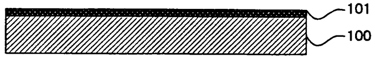
본 발명의 실시예 1은 특정 패턴의 형성에 적합한 기판 구조에 관한 것이다. 도 1에 본 실시예 1의 기판 외형도를 도시한다. 도 1a는 평면도이고, 도 1b는 도 1a를 절단면 A-A에서 본 도면이다. 도 1에 도시하는 바와 같이, 본 실시예 1의 기판(1a)은 기대의 패턴 형성면에, 패턴 형성 영역(10)이 패턴 비형성 영역(11)의 사이에 패턴화되어 배치되어 있다. 패턴 형성 영역(10)은 소정의 유동체를 부착시켜 박막을 형성시키기 위한 영역이다. 패턴 비형성 영역(11)은 상기 박막을 형성시키지 않는 영역이다. 패턴 비형성 영역(11)은 기대가 유동체에 대하여 상대적으로 비친화성을 보이는 재료로 형성되어 있을 경우에는 기대 표면 그 자체가 나타나 있는 영역이 된다. Embodiment 1 of the present invention relates to a substrate structure suitable for forming a specific pattern. 1 shows an outline of the substrate of the first embodiment. FIG. 1A is a plan view, and FIG. 1B is a view of FIG. 1A seen from the cut plane A-A. As shown in FIG. 1, in the board | substrate 1a of Example 1, the pattern formation area |
패턴 형성 영역(10)은 유동체에 대하여 상대적으로 친화성을 보이는 친화성 영역(110)과 유동체에 대하여 상대적으로 비친화성을 보이는 비친화성 영역(111)이 교대로 배치되어 구성된다. 친화성 영역(110)과 비친화성 영역(111)을 교대로 배치함으로써, 적절한 량의 유동체를 부착시킬 수 있기 때문이다. 단, 패턴 형성 영역 전체를 친화성 영역(110)만으로 구성해도 된다. The
친화성 영역(110)은 도 2a와 같이 사각형 영역이 서로 접하고 있는 패턴이나, 도 2d와 같이 사각형 영역이 일정 간격으로 배치되어 있는 패턴을 이용할 수 있다. 또, 도 2b와 같이 원형 영역이 서로 접하고 있는 패턴이나, 도 2e와 같이 원형 영역이 일정 간격으로 배치되어 있는 패턴도 이용할 수 있다. 더욱이, 도 2c 에 도시하는 바와 같이 삼각형 영역이 서로 접하고 있는 패턴이나, 도 2f와 같이 삼각형 영역이 일정 간격으로 배치되어 있는 패턴도 이용할 수 있다. 게다가, 도 2g와 같이 평행선으로 이루어지는 패턴을 생각할 수 있다. 이들 외 임의의 다각형이나 불규칙한 형상 등을 이용할 수 있다. The
여기서, 친화성을 보일지 비친화성을 보일지는 패턴 형성 대상인 유동체가 어떠한 성질을 구비하고 있는지로 결정된다. 예를 들면 유동체가 물과 같이 극성 분자를 포함하는 것이면, 극성기를 구비한 표면 영역이 친화성을 보이며, 극성기를 구비하지 않는 표면 영역이 비친화성을 보인다. 반대로 유동체가 많은 유기 매체와 같이 극성 분자를 포함하지 않는 것이면, 극성기를 구비한 표면 영역이 비친화성을 보이고, 극성기를 구비하지 않는 표면 영역이 친화성을 보인다. 유동체를 무엇으로 할지는, 박막을 어떠한 재료로 형성하는 것인가에 의해 정해진다. 본 실시예에서는, 패턴 비형성 영역(11)은 유동체에 대하여 상대적으로 비친화성을 보이도록 기대의 재료가 정해진다. 패턴 형성 영역(10)의 비친화성 영역(111)은 패턴 비형성 영역(11)과 마찬가지로 기대의 표면이 노출하고 있는 부분이다. Here, it is determined by what kind of property the fluid which is a pattern formation object has whether affinity or non-affinity is shown. For example, if the fluid contains polar molecules such as water, the surface area with polar groups shows affinity, and the surface area without polar groups shows affinity. On the contrary, if the fluid does not contain polar molecules such as many organic media, the surface region with polar groups shows affinity, and the surface region without polar groups shows affinity. What to make a fluid is determined by what material a thin film is formed. In the present embodiment, the material of the base is determined so that the
표 1에, 본 실시예의 패턴 비형성 영역(11) 및 비친화성 영역(111)으로서 사용 가능한 재료와, 친화성 영역(110)으로서 사용 가능한 재료의 예를 도시한다.
Table 1 shows an example of the material that can be used as the
[표 1]
패턴 형성 영역(10)의 형상, 배치, 크기 등은 용도에 따라서 임의로 설정할 수 있다. 도 1a에 도시한 패턴 형성 영역(10)은 사각형을 하고 있으며 규칙적으로 배치되어 있다. 물론, 패턴 형성 영역의 형상으로서는 사각형 외에 다각형이나 원형, 불규칙한 외형을 하고 있어도 된다. 또, 도 3에 도시하는 바와 같이, 패턴 형성 영역(10)을 문자나 기호, 그 밖의 도형으로 형성해도 된다. 유동체를 문자나 기호 등의 형상으로 부착시켜 박막화시키고 싶은 경우에 이용할 수 있다. 또, 패턴 형성 영역의 배치는 규칙적인 것일 필요는 없으며, 불규칙한 것이어도 된다. 패턴 형성 영역의 크기는 특별히 제한을 두지 않고, 각종 확대 축소가 가능하다. TABLE 1
The shape, arrangement, size, and the like of the
삭제delete
(작용) (Action)
도 5 및 도 6에, 종래의 기판에 대하여 유동체를 부착시킨 경우의 액체 방울 부착의 모양을 도시한다. 도 5a는 기대(100)에 액체 방울(12)을 여러 방울 토출한 경우의 단면도이고, 도 6a는 그 평면도이다. 본 실시예와 같이 패턴 형성 영역을 형성하고 있지 않는 기판에 액체 방울(12)을 연속하여 토출하면, 도 5a와 같이 착탄한 액체 방울이 표면 장력에 의해 넓어져, 인접하는 액체 방울(12)이 연결한다. 이 때, 액체 방울(12)의 넓이를 저지하는 경계가 아무 것도 없기 때문에, 도 6a에 도시하는 바와 같이, 각 액체 방울의 윤곽이 착탄했을 때의 넓이를 넘어 넓어져버린다. 유동체의 용매 성분이 적을 경우, 이 윤곽이 넓어진 채로 고화하기 때문에 미세한 패턴을 형성하는 것은 곤란해진다. 용매 성분이 많을 경우, 액체 방울을 건조시키면 액체 방울 중의 용매 성분이 제거되어, 각 액체 방울은 착탄한 위치에서 수축해 간다. 부착 위치에 제한이 없기 때문에, 도 5b 및 도 6b에 도시하는 바와 같이, 처음 연결하고 있던 액체 방울(12)이 분리되어, 아일랜드(12b)가 된다. 아일랜드(12b)가 되어 분리해 버리는 것으로는, 패턴으로서 도움이 되지 않는다. 5 and 6 show the state of liquid droplet adhesion when a fluid is attached to a conventional substrate. FIG. 5: A is sectional drawing at the time of ejecting several droplets of the
도 4를 참조하여 본 실시예의 패턴 형성 영역(10)에서의 기판(1a)의 작용을 설명한다. 도 4a는 도 2a의 패턴에 유동체의 액체 방울을 부착시켰을 때의 기판 상에 있어서의 액체 방울의 형태를 도시한다. 도 4b는 도 2g의 패턴에 유동체의 액체 방울을 부착시켰을 때의 기판 상에서의 액체 방울의 형태를 도시한다. 도 4a 및 도 4b에서의 어느 패턴의 경우에도, 잉크젯 방식에 의해 라인(L3)을 따라 액체 방울을 부착시킨 것으로 한다. Referring to Fig. 4, the operation of the substrate 1a in the
도 4a에 도시하는 바와 같이, 기판 상에 착탄한 액체 방울(12)은 친화성 영역(110)에서는 충분히 넓어진다. 그러나 비친화성 영역(111)으로부터는 배제되어, 표면 장력에 따라서 인접하는 친화성 영역(110)으로 들어간다. 따라서 표면 장력이 기능하여 들어간 후는 도 4a에 도시하는 바와 같이, 친화성 영역(110)에만 액체 방울(12)이 부착한다. 헤드로부터의 액체 방울의 토출 방향이 다소 어긋나도, 라인(L2)에서 (L4)까지의 일정 폭으로 착탄하면, 부착하는 액체 방울(12)은 항상 라 인(L2)에서 (L4)의 사이의 친화성 영역(110)에 놓인다. 친화성 영역(110)은 서로 분리하고 있든지 한 점에서 접하고 있을 뿐이기 때문에, 직접 착탄하지 않는 한, 하나의 친화성 영역(110)에 실은 액체 방울(12)이 인접하는 친화성 영역(110)에 침입할 일이 없다. 액체 방울(12)이 놓여 있는 친화성 영역(110) 옆에는, 반드시 액체 방울(12)이 놓여 있는 친화성 영역(110)이 접하고 있든지 조금 떨어져 있기 때문에, 액체 방울(12)끼리가 표면 장력으로 서로 연결된다. 따라서 액체 방울(12)이 착탄한 궤적을 따라 연결되어, 패턴이 연속한다. 액체 방울(12)이 놓인 친화성 영역(110)에서는 액체 방울이 찬 상태가 되어 있기 때문에, 이 액체 방울이 건조해도 연결하고 있던 인접하는 액체 방울과 분리되는 일은 없다. As shown in FIG. 4A, the
이상으로 알 수 있듯이, 본 실시예와 같이 형성한 패턴 형성 영역(10)에서는, 유동체를 부착시킨 영역에서는 충분히 유동체가 넓어지지만 그 이상으로 넓어지는 일이 없다. 즉, 적당량의 유동체를 부착시킬 수 있다. 친화성 영역(110)의 패턴 배치는 개개의 패턴이 서로 점 접촉하는 정도가 바람직하다. 개개의 패턴이 접촉하여 완전히 연결되면, 친화성 영역 경계에 있어서의 표면 장력의 저지가 가능하지 않아, 인접하는 친화성 영역에 무제한으로 액체 방울이 침입할 우려가 있기 때문이다. 반대로 점 형상 패턴이 너무 떨어지면, 액체 방울의 연속성이 저해되어, 액체 방울 패턴의 분리를 일으키기 때문이다. As can be seen from the above, in the
한편, 도 4b의 선 형상 패턴에서는, 액체 방울(12)이 라인(L3)을 따라 착탄하고 있으며, 인접하는 액체 방울(12)과 연결되어 있다. 이 선 형상 패턴에서는 액체 방울(12)이 라인(L2)에서 (L4)의 사이에 착탄하는 한, 라인(L3)을 중심하는 액체 방울의 연결에 흡수되어, 라인(L2)에서 (L4)의 폭보다 액체 방울이 넓어지지 않는다. 또, 라인(L3)은 연속하고 있기 때문에, 서로 겹치도록 액체 방울(12)이 착탄하는 한, 액체 방울 패턴이 분단되는 일은 없다. On the other hand, in the linear pattern of FIG. 4B, the
본 실시예의 기판(1)을 사용하여 패턴을 형성할 경우에는, 유동체를 기판면에 부착시킬 수 있는 모든 방법을 적용할 수 있다. 예를 들면 잉크젯 방식으로 부착시키는 외에, 스핀 코팅, 롤 코팅, 다이 코팅, 스프레이 코팅 등 각종 도포법을 적용할 수 있다. 본 실시예의 기판에 의하면, 적절한 액량의 유동체를 부착 가능하게 구성되어 있기 때문에, 패턴 형성 영역(10)에는 남김 없이 유동체가 부착하지만, 패턴 비형성 영역(11)에는 부착하지 않고, 패턴대로 유동체를 부착시킬 수 있다. 유동체를 부착시켰으면 열처리 등을 행하여 유동체로부터 용매를 증발시켜 박막화시킴으로써, 패턴 형성 영역대로 박막을 형성할 수 있다. When the pattern is formed using the substrate 1 of the present embodiment, any method capable of attaching the fluid to the substrate surface can be applied. For example, various coating methods, such as spin coating, roll coating, die coating, and spray coating, can be applied in addition to the ink jet method. According to the substrate of the present embodiment, the fluid is attached to the
상기한 바와 같이 본 실시예 1에 의하면, 패턴 형성 영역에는 적당량의 유동체를 부착시킬 수 있으며, 그 이외의 패턴 비형성 영역에는 유동체가 부착하지 않기 때문에, 패턴 형성 영역대로 박막을 형성할 수 있다.As described above, according to the first embodiment, an appropriate amount of fluid can be attached to the pattern formation region, and since the fluid does not adhere to other pattern non-formation regions, the thin film can be formed in the pattern formation region.
(실시예 2) (Example 2)
본 발명의 실시예 2는 파라핀 등의 유기 물질을 사용한 상기 실시예 1에서 설명한 기판 제조 방법에 관한 것이다. Example 2 of the present invention relates to the substrate manufacturing method described in Example 1 using an organic material such as paraffin.
도 7을 참조하여 본 실시예의 제조 방법을 설명한다. 도 7은 본 발명의 기판 제조 공정 단면도이다. The manufacturing method of this embodiment is demonstrated with reference to FIG. 7 is a cross-sectional view of the substrate manufacturing process of the present invention.
파라핀층 형성 공정(도 7a): 파라핀층 형성 공정은 기대(100)에 파라핀을 도포하여 파라핀층(101)을 형성하는 공정이다. 기대(100)는 유동체에 따라서 유동체에 대하여 친화성으로 할지 비친화성(소수성, 친유성)으로 할지를 선택한다. 유동체가 극성 분자를 포함하지 않을 경우에는, 기대(100)를 친수성으로 한다. 유동체가 극성 분자를 포함할 경우에는, 기대(100)를 소수성 재료로 고른다. 도 7에서는, 유동체가 극성 분자를 포함하지 않을 경우의 패턴 형성을 도시하며, 기대(100)로서는 친화성인 것을 사용하고 있다. 예를 들면, 기대(100)는 폴리-4-비닐 피롤리돈, 폴리에틸렌 옥사이드, 폴리비닐 알코올, 셀룰로오스, 폴리 아세트산 비닐 등을 사용한다. 파라핀층(101) 형성에는 롤 코팅법, 스핀 코팅법, 스프레이 코팅법, 다이 코팅법, 바 코팅법 등의 각종 도포법, 각종 인쇄법, 전사법 등의 방법을 적용할 수 있다. Paraffin layer formation process (FIG. 7A): The paraffin layer formation process is a process of forming the
에너지 공급 공정(도 7b): 마스크 형성 공정은 유동체가 극성 분자를 포함하지 않을 경우, 파라핀층(101) 중 패턴 비형성 영역(11) 및 패턴 형성 영역(10) 중의 비친화성 영역(111)에 에너지를 공급하여 파라핀을 증발시키는 공정이다. 에너지로서는 광, 열 또는 광 및 열의 3자를 생각할 수 있지만, 특정 미세 영역의 파라핀을 제거하기 위해 레이저 광을 사용하는 것이 바람직하다. 예를 들면, 단파장인 레이저 광을 조사하여 파라핀을 증발시킨다. Energy supply process (FIG. 7B): When the fluid does not contain polar molecules, the mask formation process is performed on the
이상의 제조 공정에 의해, 패턴 형성 영역(10)의 친화성 영역(110)에 파라핀층(101)이 남는다. 이 기판에 극성 분자를 포함하지 않는 유동체를 부착시키면, 패턴 형성 영역(10)에만 부착한다. 또한, 부착시키는 유동체가 극성 분자를 포함할 경우에는, 패턴 형성 영역(10) 중의 친화성 영역(110)에만 에너지를 공급하여 파라핀을 제거한다. 이로써 친화성 영역(110)에만 극성 분자를 포함하는 유동체를 부착시킬 수 있다. By the above manufacturing process, the
또한, 기대(100)가 유동체에 대하여 상대적으로 친화성을 나타내는 재료로 형성되어 있을 경우에는, 파라핀이 패턴 비형성 영역(11) 및 패턴 형성 영역(10)의 비친화성 영역(111)에 남도록 제조한다. 기대(100)가 유동체에 대하여 상대적으로 비친화성을 나타내는 재료로 형성되어 있을 경우에는, 파라핀이 패턴 형성 영역(10)의 친화성 영역(110)에 남도록 제조한다. In addition, when the
(실시예 3) (Example 3)
본 발명의 실시예 3은 상기 실시예 1에서 설명한 기판 제조 방법에 관한 것이다. 특히, 본 형태에서는 유황 화합물의 자기 집합화 단일 분자막을 이용한다. Example 3 of the present invention relates to the substrate manufacturing method described in Example 1 above. In particular, in this embodiment, the self-aggregation single molecular membrane of a sulfur compound is used.
본 실시예에서는, 기대에 금속층을 설치하여 그것을 유황 화합물을 포함하는 용해액에 침지하여 자기 집합화 단일 분자막을 형성한다. 유황 화합물은 머캅토기를 구비하는 분자로 구성된다. 이 유황 화합물을 1 내지 10mM의 에탄올 용액에 용해한다. 이 용액에 금막을 형성한 기판을 침지하여, 실온에서 1시간 정도 방치하면, 유황 화합물이 금막 표면에 자발적으로 집합해 온다. 그리고 금 원자와 유황 원자가 공유 결합적으로 결합하여, 금의 표면에 2차원적으로 유황 분자의 단일 분자막이 형성된다. 이 막의 두께는 유황 화합물의 분자량에도 의하지만, 10 내지 50옹스트롬 정도이다. 유황 화합물의 조성을 조정함으로써, 자기 집합화 단일 분자막을 유동체에 대하여 친화성으로 하거나 비친화성으로 하거나 자유롭게 설정할 수 있다. In this embodiment, a metal layer is provided on the base and immersed in a solution containing a sulfur compound to form a self-aggregating single molecular film. Sulfur compounds are composed of molecules having a mercapto group. This sulfur compound is dissolved in 1 to 10 mM ethanol solution. When the board | substrate which formed the gold film was immersed in this solution, and left to stand at room temperature for about 1 hour, a sulfur compound will spontaneously gather on the surface of a gold film. The gold atom and the sulfur atom are covalently bonded to each other to form a single molecular film of sulfur molecules two-dimensionally on the surface of the gold. The thickness of the film depends on the molecular weight of the sulfur compound, but is about 10 to 50 angstroms. By adjusting the composition of the sulfur compound, the self-aggregating single molecular membrane can be set to be affinity, non-affinity or free setting for the fluid.
유황 화합물로서는 티올 화합물이 바람직하다. 여기서 티올 화합물이란, 머캅토기(-SH;mercapt group)를 갖는 유기 화합물(R-SH;R은 알칼기(alkyl group) 등의 탄화 수소기)의 총칭을 말한다. As a sulfur compound, a thiol compound is preferable. Here, a thiol compound refers to the general term of the organic compound (R-SH; R is a hydrocarbon group, such as an alkyl group) which has a mercapto group (-SH; mercapt group).
표 2에, 유동체가 극성 분자를 포함할 경우와, 극성 분자를 포함하지 않을 경우로 나누어, 유동체에 친화성이 있는 티올 화합물의 대표적인 조성을 나타낸다. n, m은 자연수로 한다. Table 2 shows the typical composition of the thiol compound having affinity for the fluid, divided into the case where the fluid contains a polar molecule and the case where the fluid does not contain a polar molecule. n and m are natural numbers.
[표 2]
표 2에서 알 수 있듯이, 유황 화합물 단일 분자막을 극성 분자에 대하여 친화성으로 하거나 비극성 분자에 대하여 친화성으로 하거나는 조성을 바꿈으로써 자유롭게 설정할 수 있다. 도 8에, 본 실시예 3에서의 기판 제조 방법의 제조 공정 단면도를 도시한다. TABLE 2
As can be seen from Table 2, the sulfur compound single molecule membrane can be freely set by affinity for polar molecules or affinity for nonpolar molecules, or by changing the composition. 8, the manufacturing process sectional drawing of the board | substrate manufacturing method in Example 3 is shown.
삭제delete
금속층 형성 공정(도 8a): 금속층 형성 공정은 기대(100) 상에 금속층(102)을 형성하는 공정이다. 기대(100)는 유동체에 따라서 유동체에 대하여 친화성으로 할지 비친화성(소수성, 친유성)으로 할지를 선택한다. 유동체가 극성 분자를 포함하지 않을 경우에는, 기대(100)를 친수성으로 한다. 유동체가 극성 분자를 포함할 경우에는, 기대(100)를 소수성 재료로 고른다. 금속층(102)으로는, 화학적·물리적인 안정성에서 금(Au)이 바람직하다. 금 외에, 유황 화합물을 화학적으로 흡착하는 은(Ag), 동(Cu), 인듐(In), 갈륨-비소(Ga-As) 등의 금속이어도 된다. 금속층(102)의 형성 방법으로서는, 습식 도금, 진공 증착법, 진공 스퍼터법 등의 공지의 기술을 사용할 수 있다. 단, 금속의 박막을 일정 두께로 균일하게 형성할 수 있는 성막법이면, 그 종류에 특별히 한정되는 것은 아니다. 금속층의 역할은 유황 화합물층을 고정하는 것이기 때문에, 금속층 자체는 극히 얇아도 된다. 그 때문에 500 내지 2000옹스트롬 정도의 두께로 형성하면 된다. Metal layer formation process (FIG. 8A): A metal layer formation process is a process of forming the
또한, 기판(100)에 따라서는 금속층(102)과 기대(100)와의 밀착성이 나빠진다. 이러한 경우에는 금속층(102)과 기대(100)와의 밀착성을 향상시키기 위해, 기대와 금속과의 사이에 중간층을 형성한다. 중간층은 기대(100)와 금속층(102)과의 사이 결합력을 강화시키는 소재, 예를 들면, 니켈(Ni), 크롬(Cr), 탄탈(Ta) 노즐 혹은 그들 합금(Ni-Cr 등)인 것이 바람직하다. 중간층을 설치하면, 기대(100)와 금속층(102)과의 결합력이 증대해, 기계적인 마찰에 대하여, 유황 화합물층이 박리하기 어려워진다. 금속층(102) 아래에 중간층을 형성할 경우에는, 예를 들면 Cr을 100 내지 300옹스트롬 두께로 진공 스퍼터법, 또는 이온 플레팅법에 의해 형성한다. Moreover, depending on the board |
패턴 형성 공정(도 8b): 패턴 형성 공정은 기대(100) 상에 형성한 금속층(102) 중 일부에 에너지를 부여해 금속을 증발시킨다. 유동체가 극성 분자를 포함하여 기대(100)가 소수성을 보일 경우, 또는 유동체가 극성 분자를 포함하 지 않고 기대(100)가 친수성을 보일 경우에는, 패턴 비형성 영역(11) 및 패턴 형성 영역(10) 중의 비친화성 영역(111)에 에너지를 공급한다. 유동체가 극성 분자를 포함하지 않고 기대(100)가 소수성을 보일 경우, 또는 유동체가 극성 분자를 포함하여 기대(100)가 친화성을 보일 경우에는, 패턴 형성 영역(10) 중의 친화성 영역(110)에만 에너지를 공급한다. 에너지로서는 광이 바람직하며, 특히 단파장의 고 에너지를 공급 가능한 레이저 광이 바람직하다. 픽 업(200)을 친화성 영역 또는 비친화성 영역의 패턴에 합쳐서 레이저 광을 사출시키면서 이동시킨다. 레이저 광이 조사된 영역은 금속층(102)을 형성하는 금속이 증발하기 때문에, 기대(100)가 노출한다. Pattern Forming Step (FIG. 8B): The pattern forming step applies energy to a portion of the
유황 화합물 침지 공정(도 8c): 유황 화합물 침지 공정은 일부 금속이 제거된 금속층을 포함하는 기판을 유황 화합물의 용해액에 침지하여, 자기 집합화 단일 분자막(103)을 형성하는 공정이다. 우선, 자기 집합화 단일 분자막(103)에 사용하고 싶은 조성의 티올 화합물을 에탄올 또는 이소프로필 알코올과 같은 유기 용제에 녹인 용액을 준비한다. 예를 들면 유동체가 극성 분자를 포함하여 해당 자기 집합화 단일 분자막(103)을 친화성 영역(110)으로 하고 싶을 경우에는, OH기 또는 CO2H기를 갖는 유황 화합물을 사용하여 친화성 유황 화합물 용액을 제조한다. 유동체가 극성 분자를 포함하지 않고 해당 자기 집합화 단일 분자막(103)을 친화성 영역(110)으로 하고 싶을 경우에는, 알킬기를 갖는 유황 화합물을 사용하여 소수성 유황 화합물 용액을 제조한다. 그리고 그 용액 중에 금속층(102)을 패터닝한 기대(100)를 침지한다. 침지 조건은 용액의 유황 화합물 농도가 0.01mM에서, 용액 온도가 상온으로부터 50℃ 정도, 침지 시간이 5분에서 30분 정도로 한다. 침지 처리 동안, 유황 화합물층의 형성을 균일하게 행하도록, 용액의 각반 또는 순환을 행한다. Sulfur Compound Dipping Process (FIG. 8C): The sulfur compound dipping process is a process of forming a self-aggregating single
금속 표면의 청정함만 유지할 수 있으면, 유황 분자가 스스로 자기 집합화하여 단일 분자막을 형성하기 때문에, 엄격한 조건 관리가 불필요한 공정이다. 침지가 종료할 즈음에는, 금 표면에만 강고한 부착성을 갖는 유황 분자의 단일 분자막이 형성된다. If only the cleanness of the metal surface can be maintained, since the sulfur molecules self-aggregate to form a single molecular film themselves, a strict condition management is unnecessary. At the end of the immersion, a single molecular film of sulfur molecules having firm adhesion only to the gold surface is formed.
마지막으로 기대 표면에 부착한 용해액을 세정하여 제거한다. 금층 이외의 부분에 부착한 유황 화합물 분자는 공유 결합을 하고 있기 않기 때문에, 에틸 알코올에 의한 린스 등, 간단한 세정에 의해 제거된다. Finally, the dissolved solution attached to the base surface is washed and removed. Sulfur compound molecules attached to portions other than the gold layer are not covalently bonded, and are thus removed by simple washing such as rinsing with ethyl alcohol.
이상의 공정에 의해, 자기 집합화 단일 분자막(103)이 패턴 형성 영역(10) 중의 친화성 영역(110)에 형성된 기판(1)이 제조된다. By the above process, the board | substrate 1 in which the self-assembly single
상기한 바와 같이, 본 실시예(3)에 의하면, 유황 화합물의 자기 집합화 단일 분자막을 사용함으로써, 액상 재료를 안정시켜 패턴을 따라 부착시킬 수 있는 기판을 제조할 수 있다. 특히, 유황 화합물의 자기 집합화 단일 분자막은 마모에 강하고, 물리적, 화학적 내성이 높기 때문에, 공업 용품인 기판에 적합하다. 또, 유황 화합물을 선택하면, 기대의 성질에 따라서 자유롭게 자기 집합화 단일 분자막을 친수성으로도 비친수성으로도 할 수 있다. 더욱이, 레이저 광을 사용하면, 미세한 패턴을 형성할 수 있다. As described above, according to the present embodiment (3), by using the self-aggregating single molecular film of the sulfur compound, it is possible to manufacture a substrate which can stabilize the liquid material and adhere it along the pattern. In particular, self-aggregating single molecular films of sulfur compounds are suitable for substrates that are industrial articles because they are resistant to abrasion and have high physical and chemical resistance. In addition, when the sulfur compound is selected, the self-aggregating single molecular membrane can be made hydrophilic or non-hydrophilic freely depending on the properties of the base. Furthermore, by using laser light, a fine pattern can be formed.
또한, 기대(10O)가 유동체에 대하여 상대적으로 친화성을 나타내는 재료로 형성되어 있을 경우에는, 비친화성을 보이는 자기 집합화 단일 분자막이 패턴 비형성 영역(11) 및 패턴 형성 영역(10)의 비친화성 영역(111)에 남도록 제조한다. 기대(100)가 유동체에 대하여 상대적으로 비친화성을 나타내는 재료로 형성되어 있을 경우에는, 친화성을 보이는 자기 집합화 단일 분자막이 패턴 형성 영역(10)의 친화성 영역(110)에 남도록 제조한다. In addition, when the
(실시예 4)(Example 4)
본 발명의 실시예 4는 플라즈마 처리에 의한 실시예 1의 기판 제조 방법에 관한 것이다. Example 4 of the present invention relates to a method of manufacturing a substrate of Example 1 by plasma treatment.
플라즈마 처리는 소정의 기압 하에서 고전압의 글로우 방전을 행하여 기판의 표면 개량을 행하는 방법이다. 유리나 플라스틱과 같은 절연성 기판에 플라즈마 처리를 행하면, 기판 표면에 다량의 미반응기와 가교층이 발생한다. 이것을 대기 또는 산소 분위기에 노출하면 미반응기가 산화되어 카르보닐기, 수산기를 형성할 수 있다. 이들은 극성기이기 때문에 극성 분자를 포함하는 유동체에 대하여 친화성이 있다. 한편, 유리나 플라스틱의 대부분은 극성 분자를 포함하는 유동체에 대하여 비친화성을 나타낸다. 따라서, 기판의 패턴 형성면을 선택적으로 플라즈마 처리함으로서 친화성 영역 및 비친화성 영역을 생성할 수 있다. 본 실시예에서는 이 원리에 근거하여, 마스크를 실시함으로써 일부 영역만을 플라즈마 처리하여, 친화성 영역과 비친화성 영역을 출현시킨다. Plasma treatment is a method of improving the surface of a substrate by performing a glow discharge of high voltage under predetermined | prescribed atmospheric pressure. Plasma treatment on an insulating substrate such as glass or plastic generates a large amount of unreacted groups and crosslinked layers on the surface of the substrate. Exposure to atmospheric or oxygen atmosphere can oxidize unreacted groups to form carbonyl groups and hydroxyl groups. Because they are polar groups, they are affinity for fluids containing polar molecules. On the other hand, most glass or plastics exhibit incompatibility with fluids containing polar molecules. Therefore, the affinity region and the non-affinity region can be generated by selectively plasma-processing the pattern formation surface of a board | substrate. In this embodiment, based on this principle, only a part of the region is subjected to a plasma treatment by applying a mask so that the affinity region and the non-affinity region appear.
다음으로 도 9를 참조하여 본 실시예 4의 기판 제조 방법을 설명한다. Next, the board | substrate manufacturing method of Example 4 is demonstrated with reference to FIG.
마스크 형성 공정(도 9a): 마스크 형성 공정은 기대(100) 상에 마스크(201)를 실시하는 공정이다. 기대(100)로서는, 플라즈마 조사에 의해 미반응기가 출현할 수 있는 소재, 소정의 플라스틱, 표면을 테플론 가공된 유리 기판 등을 사용한다. 마스크(201)는 기대(100) 상에서 소수성으로 하고 싶은 영역만 마스크가 덮어지도록 패턴 형성된다. 예를 들면 유동체로서 극성 분자를 포함하는 것을 사용할 경우에는, 패턴 비형성 영역(11) 및 패턴 형성 영역(10) 중의 비친화성 영역(111)이 노광되는 마스크를 설치한다. 마스크 재료로서는, 노광 마스크, 이멀젼 마스크, 하드 마스크 등 각종 마스크를 형성할 수 있다. 노광 마스크를 사용할 경우에는, 크롬, 산화 크롬, 실리콘, 산화 실리콘, 산화막 등을 진공 증착, 스퍼터링, CVD법 등으로 형성한다. Mask Forming Step (FIG. 9A): The mask forming step is a step of applying a
플라즈마 조사 공정(도 9b): 플라즈마 조사 공정은 마스크(201)가 실시된 기대(100) 상에 플라즈마(202)를 조사하는 공정이다. 플라즈마 조사는 예를 들면 10-1 내지 100Pa의 아르곤 가스 속에서 네온 트랜스를 사용하여, 수백 볼트에서 수천 볼트의 전압을 인가하여 글로우 방전시켜 행한다. 이 밖에, 라디오 주파수대의 방전 전원을 사용하여 용량 결합 또는 유전 결합에 의해 방전 플라즈마를 형성하는 방법, 마이크로파 전력을 도파관에 의해 방전 용기에 공급하여 방전 플라즈마를 형성시키는 방법 등을 적용할 수 있다. Plasma irradiation step (FIG. 9B): The plasma irradiation step is a step of irradiating the plasma 202 on the base 100 on which the
이 처리에 의해, 플라즈마 속에 활성 입자로서 이온, 전자, 여기 원자 또는 분자 및 레디컬 등이 발생하여, 기대(100) 표면의 고분자 분자 구조가 변화한다. 즉, 플라즈마(202)가 조사된 부분에 다량의 미반응기나 가교층이 출현한다. By this treatment, ions, electrons, excitation atoms or molecules, radicals, and the like are generated as active particles in the plasma, and the polymer molecular structure on the surface of the
표면 개질 공정(도 9c): 표면 개질 공정은 플라즈마 처리된 기대(100) 표면을 산화하여 표면을 개질하는 공정이다. 상기 플라즈마 처리에 의해 미반응기나 가교층이 출현한 기대(100)를 대기 또는 산소 분위기 하에 노출시킨다. 기대(100) 표면의 미반응기는 산화되어, 수산기나 카르보닐기 등의 극성기(104)를 초래한다. 이들 극성기(104)는 물에 대하여 젖기 쉬운 친수성을 보인다. 한편, 마스크되어 플라즈마 처리되지 않은 영역은 플라스틱인 채이며 비친수성을 보인다. Surface Modification Process (FIG. 9C): The surface modification process is a process of oxidizing the surface of the base 100 treated with plasma to modify the surface. The base 100 in which the unreacted group or the crosslinked layer appears by the plasma treatment is exposed in the atmosphere or oxygen atmosphere. Unreacted groups on the surface of the base 100 are oxidized, resulting in
삭제delete
따라서, 플라즈마 처리된 영역이 친화성 영역(110)이 되고, 플라즈마 처리되지 않은 영역이 비친화성 영역(111) 또는 패턴 비형성 영역(11)이 된다. Thus, the plasma treated region becomes the
상기한 바와 같이 본 실시예 4에 의하면, 플라즈마 처리에 의해 기대를 구성하는 일부 영역의 분자 구조를 변경함으로써, 비친화성 막을 친화성 막으로 변경할 수 있기 때문에, 새로운 층을 형성하지 않고 실시예 1의 기판을 제공할 수 있다. 분자 레벨의 조성이 변경되기 때문에 이 기판은 안정적이다. As described above, according to the fourth embodiment, since the non-affinity film can be changed to the affinity film by changing the molecular structure of some regions constituting the base by the plasma treatment, the first layer of Example 1 is not formed. A substrate can be provided. The substrate is stable because the composition of the molecular level changes.
또한, 기대(100)가 유동체에 대하여 상대적으로 친화성을 나타내는 재료로 형성되어 있을 경우에는, 패턴 비형성 영역(11) 및 패턴 형성 영역(10)의 비친화성 영역(111)에 플라즈마 조사되도록 제조한다. 기대(100)가 유동체에 대하여 상대적으로 비친화성을 나타내는 재료로 형성되어 있을 경우에는, 패턴 형성 영역(10)의 친화성 영역(110)이 플라즈마 조사되도록 제조한다. In addition, when the
(실시예 5) (Example 5)
본 발명의 실시예 5는 자외선 조사에 의한 실시예 1의 기판 제조 방법에 관 한 것이다. Example 5 of the present invention relates to the substrate manufacturing method of Example 1 by ultraviolet irradiation.
자외선 조사는 수지의 표면 개질 수단으로서 상기 플라즈마 처리와 동일하게 사용할 수 있다. 기판이 폴리에스테르나 폴리에틸렌과 같은 수지로 형성되어 있거나 이들 수지 박막으로 덮어져 있거나 하면, 이들 수지는 극성이 없는 유기 고분자이기 때문에, 본래 그 표면은 극성 분자를 포함하는 유동체에 대하여 비친화성으로, 극성 분자를 포함하지 않는 유동체에 대하여 친화성이 된다. 그런데 이 수지 표면에 자외선을 조사하면, 플라즈마 처리와 동일하게 표면이 활성화하여, OH기나 COOH기가 출현한다. 이들 기는 극성기이기 때문에 극성 분자를 포함하는 유동체에 대하여 친화성을 나타내게 된다. 기판의 패턴 형성면 중 마스크로 선택적으로 자외선을 조사시킴으로써, 친화성 영역과 비친화성 영역을 용이하게 형성할 수 있다. Ultraviolet irradiation can be used in the same manner as the plasma treatment as the surface modification means of the resin. If the substrate is formed of a resin such as polyester or polyethylene, or covered with a thin film of these resins, since these resins are organic polymers having no polarity, the surface is inherently unaffinity with respect to fluids containing polar molecules and thus polar. It becomes affinity for fluids that do not contain molecules. When ultraviolet rays are irradiated onto the surface of the resin, however, the surface is activated in the same manner as in the plasma treatment, and OH groups and COOH groups appear. Since these groups are polar groups, they show affinity for fluids containing polar molecules. The affinity region and the non-affinity region can be easily formed by selectively irradiating an ultraviolet-ray with a mask among the pattern formation surfaces of a board | substrate.
다음으로 도 10을 참조하여 본 실시예 5의 기판 제조 방법을 설명한다. Next, the board | substrate manufacturing method of Example 5 is demonstrated with reference to FIG.
마스크 형성 공정(도 10a): 마스크 형성 공정은 기대(100) 상에 마스크(203)를 실시하는 공정이다. 기대(100)로서는, 플라즈마 조사에 의해 미반응기가 출현할 수 있는 소재, 특히 폴리에스테르나 폴리에틸렌 등의 플라스틱 등을 사용한다. 또는 표면에 이들 플라스틱에 의한 박막이 형성되어 있는 유리 등의 기판이어도 된다. 마스크(203)는 기대(100) 상에서 소수성으로 하고 싶은 영역만 마스크가 덮어지도록 패턴 형성된다. 예를 들면 극성 분자를 포함하는 유동체를 사용할 경우에는, 패턴 형성 영역(10) 중의 친화성 영역(110)이 노광되며, 그 이외의 영역이 덮어지는 마스크를 설치한다. 마스크 재료로서는, 노광 마스크, 이멀젼 마스크, 하드 마스크 등 각종 마스크를 형성할 수 있다. 노광 마스크를 사용할 경우에는, 크롬, 산화 크롬, 실리콘, 산화 실리콘, 산화막 등을, 진공 증착, 스퍼터링, CVD법 등으로 형성한다. Mask Forming Step (FIG. 10A): The mask forming step is a step of applying a
자외선 조사 공정(도 10b): 자외선 조사 공정은 마스크(203)가 실시된 기대(100) 상에 자외선 조사하는 공정이다. 자외선 조사에는, 예를 들면 자외선 램프를 사용하여 행한다. 이 처리에 의해, 자외선(204)이 기대(100) 표면의 고분자에 에너지를 부여해 분자를 여기시켜 공유 결합 구조를 변화시킨다. 이것에 의해 자외선(204)이 조사된 기대(100)의 노광 영역에 다량의 미반응기나 가교층이 출현한다. Ultraviolet irradiation process (FIG. 10B): An ultraviolet irradiation process is a process of irradiating an ultraviolet-ray on the base 100 with which the
표면 개질 공정(도 10c): 표면 개질 공정은 자외선 조사된 기대(100) 표면을 산화하여 표면을 개질하는 공정이다. 상기 자외선(204) 조사에 의해 미반응기나 가교층이 출현한 기대(100)를 대기 또는 산소 분위기 하에 노출시키면, 기대(100) 표면의 미반응기가 산화되어, 수산기나 카르보닐기 등의 극성기(105)가 생긴다. 이들 극성기(105)는 극성 분자를 포함하는 물 등의 유동체에 대하여 젖기 쉬운 친화성(친수성)을 보인다. 한편, 마스크되어 노광되지 않은 영역은 플라스틱 그대로의 성질을 보인다. 즉, 극성 분자를 포함하는 유동체에 대하여 비친화성을 나타낸다. 따라서, 자외선 조사된 영역이 친화성 영역(110)이 되고, 자외선 조사되지 않은 영역이 비친화성 영역(111) 또는 패턴 비형성 영역(11)이 된다. Surface modification process (FIG. 10C): The surface modification process is a process of oxidizing the surface of the base 100 that is irradiated with ultraviolet light to modify the surface. When the base 100 on which the unreacted group or the crosslinked layer has appeared by the
상기한 바와 같이 본 실시예 5에 의하면, 자외선 조사에 의해 기대를 구성하는 일부 영역의 분자 구조를 변경함으로써, 비친화성 막을 친화성 막으로 변경할 수 있기 때문에, 새로운 층을 형성하지 않고 실시예 1의 기판을 제공할 수 있다. 분자 레벨의 조성이 변경되기 때문에 이 기판은 안정적이다. As described above, according to the fifth embodiment, since the non-affinity film can be changed to an affinity film by changing the molecular structure of some regions constituting the base by ultraviolet irradiation, the first layer of Example 1 is not formed. A substrate can be provided. The substrate is stable because the composition of the molecular level changes.
또한, 기대(100)가 유동체에 대하여 상대적으로 친화성을 나타내는 재료로 형성되어 있을 경우에는, 패턴 비형성 영역(11) 및 패턴 형성 영역(10)의 비친화성 영역(111)에 자외선 조사되도록 제조한다. 기대(100)가 유동체에 대하여 상대적으로 비친화성을 나타내는 재료로 형성되어 있을 경우에는, 패턴 형성 영역(10)의 친화성 영역(110)이 자외선 조사되도록 제조한다. In addition, when the
(실시예 6)(Example 6)
본 발명의 실시예 6은 포토리소그래피법을 사용한 실시예 1의 기판 제조 방법에 관한 것이다. Example 6 of the present invention relates to the substrate manufacturing method of Example 1 using the photolithography method.
다음으로 도 11을 참조하여 본 실시예 6의 기판 제조 방법을 설명한다. 이하의 설명에서는 기대(100)가 유동체에 대하여 상대적으로 비친화성을 나타내고, 포토리소그래피법에 의해 유동체에 대하여 상대적으로 친화성을 나타내는 층을 패턴 형성 영역(10) 중의 친화성 영역(110)에 형성해 가는 것으로 한다. 단, 기대(100)가 유동체에 대하여 상대적으로 친화성을 나타낼 경우에는, 포토리소그래피법에 의해 패턴 비형성 영역(11) 및 패턴 형성 영역(10) 중의 비친화성 영역(111)에, 유동체에 대하여 상대적으로 비친화성을 나타내는 층을 형성하게 된다. Next, the board | substrate manufacturing method of Example 6 is demonstrated with reference to FIG. In the following description, the
친화성 막 형성 공정(도 11a): 친화성 막 형성 공정은 기대 표면에 유동체에 대하여 상대적으로 친화성을 나타내는 재료에 의한 박막(106)을 형성하는 공정이다. 극성 분자를 포함하는 유동체에 대하여 상대적으로 친화성을 나타내는 박막 재료로서는, OH기, COOH기, NH2기 등을 갖는 실란 커플링제 등을 들 수 있다. 박막의 형성 방법으로서는, 스핀 코팅법, 디핑법, 공지의 박막 형성 방법을 적용할 수 있다. 박막(106)의 두께는 상기 제조 방법에 의해 거의 균일한 두께로 형성할 수 있는 정도의 두께를 확보할 수 있으면 충분하다. Affinity film formation process (FIG. 11A): An affinity film formation process is a process of forming the
노광 공정(도 11b): 노광 공정은 박막(106) 상에 포토 레지스트(107)를 도포하여, 패턴 형성에 합친 마스크를 실시한 후, 노광 현상하여 포토 레지스트(107)를 남기는 공정이다. 포토 레지스트로서는, PMMA, PBS, 폴리이미드 등의 공지의 재료를 적용할 수 있고, 에칭 방법 및 박막 재료(106)와의 관계로 정한다. 포토 레지스트(107)를 스핀법, 스프레이법, 롤 코팅법, 침지법 등의 도포법으로 도포 후, 상기 실시예 4 또는 5에서 설명한 것과 동일한 마스크를 실시하여, 포토 레지스트(107)를 노광한다. 포토 레지스트가 포지티브형일 경우에는, 패턴 형성 영역(10) 중의 친화성 영역(110)을 덮는 마스크를 실시한다. 포토 레지스트가 네거티브형일 경우에는, 패턴 비형성 영역(11) 및 패턴 형성 영역(10) 중의 비친화성 영역(111)을 덮는 마스크를 실시한다. 그리고 마스크 상으로부터 통상 광 또는 원적외선 노광을 행하여 포토 레지스트를 노광한다. Exposure process (FIG. 11B): An exposure process is a process of apply | coating the
현상 공정(도 11c): 현상 공정은 노광시킨 포토 레지스트(107)를 현상하여 패턴에 합친 포토 레지스트를 남기는 공정이다. 스프레이법이나 디핑법 등에 의해 현상액을 부착시켜 현상을 행한다. 이어서 린스액을 동일한 방법으로 부착시켜 불필요한 포토 레지스트를 제거한다. 이 처리에 의해 박막(106) 상에는 패턴을 따른 포토 레지스트(107)가 남겨진다. Developing Step (FIG. 11C): The developing step is a step of developing the exposed
에칭 공정(도 11d): 에칭 공정은 포토 레지스트(107)가 남은 박막(106)을 에 칭하여 불필요한 박막(106)을 제거하는 공정이다. 에칭 방법은 웨트 에칭이나 드라이 에칭 중 어느 것이나 이용 가능하다. 웨트 에칭에 있어서의 에칭액 또는 드라이 에칭에 있어서의 에칭 가스로서는, 피에칭 재료인 박막(106) 에칭에 적합한 것이 선택된다. Etching Step (FIG. 11D): The etching step is a step of removing unnecessary
이상의 공정에 의해, 패턴 형성 영역(10) 중의 친화성 영역(110)을 제외하는 영역의 박막(106)이 제거되어, 패턴 형성 영역(10)과 패턴 비형성 영역(11)이 기대(100) 표면에 형성된다. By the above process, the
상기한 바와 같이 본 실시예 6에 의하면, 박막 패턴 형성 방법으로서 빈번하게 사용되고 있는 포토리소그래피법을 적용해도 실시예 1의 기판을 제조할 수 있다. As described above, according to the sixth embodiment, even if the photolithography method which is frequently used as the thin film pattern forming method is applied, the substrate of the first embodiment can be manufactured.
또한, 기대(100)가 유동체에 대하여 상대적으로 친화성을 나타내는 재료로 형성되어 있을 경우에는, 비친화성을 보이는 박막이 패턴 비형성 영역(11) 및 패턴 형성 영역(10)의 비친화성 영역(111)에 남도록 제조한다. 기대(100)가 유동체에 대하여 상대적으로 비친화성을 나타내는 재료로 형성되어 있을 경우에는, 친화성을 보이는 박막이 패턴 형성 영역(10)의 친화성 영역(110)에 남도록 제조한다. In addition, when the
(실시예 7)(Example 7)
본 발명의 실시예 7이 기판에 전하를 주는 것에 의한 실시예 1의 기판 제조 방법에 관한 것이다. Embodiment 7 of the present invention relates to the method of manufacturing a substrate of Example 1 by charging a substrate.
도 12에 본 실시예 7에 있어서의 기판 제조 공정 단면도를 나타낸다. 12 is a sectional view of the substrate manufacturing process in the seventh embodiment.
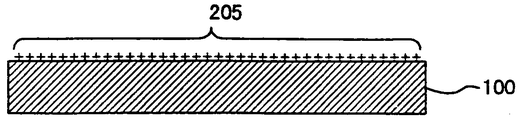
전하 인가 공정(도 12a): 전하 인가 공정도는 기대(100)에 전하를 생기게 하 는 공정이다. 기대(100)로서는 대전하기 쉬운 재료를 사용한다. 예를 들면 고분자 재료에서는, 폴리에틸렌 테레프탈레이트 등을 사용할 수 있다. 이 밖에 레이저 프린터 감광체로서 사용되는 셀렌계, Si:H계, CdS계, Zn0계 등의 무기 반도체나, PVK/Se, PVK-TNF, CGL/CTL, CTL/CGL, CTL(CGL) 등을 사용하는 것도 가능하다. 기대(100) 표면에 전하(205)를 인가하기 위해서는 레이저 프린터로 사용되는 코로나 대전기 등의 전하 인가 수단을 사용한다. 기판 표면에 이 코로나 대전기 등의 전하 인가 수단을 근접시켜 표면에 일정하게 대전시킨다. 구체적으로는 직경 50μm 내지 100μm인 텅스텐선에 6 내지 8kV의 직류 고전압을 인가하여, 기대 표면으로부터 8 내지 10mm 떨어져 코로나 방전을 행한다. Charge application process (FIG. 12A): The charge application process diagram is a process of generating charges in the
탈 차지(decharging) 공정(도 12b): 탈 차지 공정은 일정하게 대전한 기대(100)의 패턴 형성면에 선택적으로 에너지(206)를 인가하여 전하(205)를 부분적으로 이탈시키는 공정이다. 즉, 광 에너지 등이 공급됨으로써 노광부에서는, 광 캐리어의 생성과 수송이 일어나, 표면 전하가 상실하여, 표면에 정전 현상이 형성된다. 에너지 공급원으로서는 레이저 광이 바람직하다. 미세 패턴에 합쳐진 잠상 형성을 행할 수 있기 때문이다. 그 외, 마스크를 사용하여 자외선 등의 광 에너지를 가해도 된다. 탈 차지하는 영역은 상기한 바와 같이 기대(100) 재료로서 폴리에틸렌 테레프탈레이트를 사용한 경우에는, 패턴 비형성 영역(11) 및 패턴 형성 영역(10) 중의 비친화성 영역(111)으로 한다. 탈 차지된 영역은 정착 공정에 있어서 분말 재료가 정착되지 않고, 기대(100) 표면이 노출한 채로 된다. Decharging process (FIG. 12B): The decharging process is a process of partially discharging the
부착 공정(도 12c): 부착 공정은 탈 차지되지 않은 대전 영역에 정전 인력을 이용하여 분말 재료(107)를 부착시키는 공정이다. 분말 재료(107)로서는, 예를 들면 레이저 프린터에 있어서의 토너와 같은 재료를 말하며, 정전력으로 부착시키는 것이 가능한 재료를 사용한다. 또, 정착 후에는 극성 분자를 포함하는 유동체에 대하여 상대적으로 친화성을 나타내는 표면이 되는 재료를 사용한다. 이러한 재료로서는, 강철재, 유리구(球), 철분, 이들을 수지 코팅한 것, 자성체와 수지와의 혼합물 등을 이용할 수 있다. 구체적으로는, 기대(100) 상에서 대전하고 있는 영역과 역극성 분말 재료(107)가 정전 인력으로 전하(205)가 존재하고 있는 영역에 부착한다. Attachment Process (FIG. 12C): The attaching process is a process of attaching the
정착 공정(도 12d): 정착 공정은 기대(100) 표면에 부착한 분말 재료(107)를 정착시키는 공정이다. 상기 정전 인력에 의해 분말 재료(107)가 기대(100)의 대전 영역에 부착했으면, 기대(100)에 열을 가해 분말 재료(107)를 융해시켜 기대(100)에 정착시킨다. 이 결과, 패턴 형성 영역(10) 중에 분말 재료가 정착하여 이루어지는 친화성 영역(110)이 형성된다. Fixing process (FIG. 12D): A fixing process is a process of fixing the
상기한 바와 같이 본 실시예 7에서는, 기판을 탈 차지하여 분말 재료를 정착시킴으로써 친화성 영역 및 비친화성 영역을 구비한 실시예 1의 기판을 제조할 수 있다. As described above, in the seventh embodiment, the substrate of the first embodiment having the affinity region and the non-affinity region can be produced by decharging the substrate to fix the powder material.
또한, 기대(100)가 유동체에 대하여 상대적으로 친화성을 나타내는 재료로 형성되어 있을 경우에는, 비친화성을 보이는 분말 재료에 의한 박막이 패턴 비형성 영역(11) 및 패턴 형성 영역(10)의 비친화성 영역(111)에 남도록 제조한다. 기대(100)가 유동체에 대하여 상대적으로 비친화성을 나타내는 재료로 형성되어 있을 경우에는, 친화성을 보이는 분말 재료에 의한 박막이 패턴 형성 영역(10)의 친화성 영역(110)에 남도록 제조한다. In addition, when the
(실시예 8)(Example 8)
본 발명의 실시예 8은 기대에 인쇄 기술을 사용하여 직접 막을 형성해 가는 제조 방법에 관한 것이다. Embodiment 8 of the present invention relates to a manufacturing method for forming a film directly using a printing technique on an expectation.
도 13에 본 실시예 8의 기판 제조 공정 단면도를 도시한다. 도 13은 예를 들면 평판 인쇄의 일종인 오프셋 인쇄를 이용한 경우의 제조 방법을 설명하는 것이다. 13 is a sectional view of the substrate manufacturing process of the eighth embodiment. 13 illustrates a manufacturing method in the case of using offset printing, which is a type of flat printing, for example.
인쇄 공정(도 13a): 인쇄 공정은 소정의 인쇄 방법에 의해 유동체에 대하여 친화성을 갖는 막 혹은 친화성이 없는 박막을 형성하는 공정이다. 인쇄 장치는 기판과 같이 딱딱한 물질에 인쇄하는 것이 가능한 것을 요한다. 종래 인쇄와의 차이는 잉크 대신에 본 발명의 친화성 영역 또는 비친화성 유역을 형성하는 재료를 사용하는 점이다. 기대(100)가 극성 분자를 포함하는 유동체에 대하여 상대적으로 비친화성을 나타낼 경우에는, 이 인쇄 장치에 의해 패턴 형성 영역(10) 중의 친화성 영역(110)에만 재료(108)를 부착시킨다. 기대(100)가 극성 분자를 포함하는 유동체에 대하여 상대적으로 친화성을 나타낼 경우에는, 이 인쇄 장치에 의해 패턴 비형성 영역(11) 및 패턴 형성 영역(10) 중의 비친화성 영역(111)에 재료(108)를 부착시킨다. 이 도면에서는, 오프셋 인쇄 장치 중 전사 롤러(207)만을 도시하고 있다. 전사 롤러(207)로부터 기대(100)의 패턴 형성면에 박막 재료(108)가 전사된다. 인쇄 방법으로서는, 오프셋 인쇄에 의하지 않고, 직접 인쇄법 그 밖의 평판 인쇄법, 볼록판, 오목판, 구멍판, 정전기나 자기를 사용하는 방법 등을 적용하는 것이 가능하다. 즉, 공지의 인쇄 방법에 의해 잉크 대신에 박막 재료를 기대에 부착시키는 것이 가능한 인쇄 방법을 적당히 적용할 수 있다. Printing process (FIG. 13A): A printing process is a process of forming the film | membrane which has affinity with respect to a fluid, or a thin film without affinity with a predetermined printing method. The printing apparatus needs to be able to print on a hard material such as a substrate. The difference from conventional printing is that instead of ink, the material forming the affinity region or the non-affinity basin of the present invention is used. When the base 100 exhibits relatively incompatibility with a fluid containing polar molecules, the
정착 방법(도 13b): 박막 재료가 기대(100)에 전사시켜지면, 열처리 등 공지의 기술을 적용하여 박막 재료(108)를 안정화시킨다. 이 공정에 의해, 패턴 형성 영역(10)의 친화성 영역(110)에만 박막이 형성된 기판을 제조할 수 있다. Fixing Method (FIG. 13B): When the thin film material is transferred to the
상기한 바와 같이 본 실시예 8에 의하면, 공지의 인쇄법을 이용하여 박막 재료를 부착시킴으로써 실시예 1에 도시하는 바와 같은 기판을 제조할 수 있다. As described above, according to the eighth embodiment, the substrate as shown in the first embodiment can be manufactured by depositing a thin film material using a known printing method.
또한, 기대(100)가 유동체에 대하여 상대적으로 친화성을 나타내는 재료로 형성되어 있을 경우에는, 패턴 형성 영역(10)의 비친화성 영역(111)에 비친화성을 보이는 박막을 인쇄한다. 기대(100)가 유동체에 대하여 상대적으로 비친화성을 나타내는 재료로 형성되어 있을 경우에는, 패턴 형성 영역(10)의 친화성 영역(110)에 친화성을 보이는 박막을 인쇄한다.In addition, when the
(그 밖의 변형예)(Other modifications)
본 발명은 상기 실시예에 의하지 않고 여러 가지로 변형하여 적용하는 것이 가능하다. The present invention can be applied in various ways without resorting to the above embodiments.
예를 들면, 기대에 형성하는 패턴 형상이나 친화성 영역의 실시예 1에서 도시한 배치는 단순한 예시로, 각종 변경이 가능하다. 점 형상 패턴, 선 형상 패턴 모두 그 크기, 형상 및 배치를 각종 변경할 수 있다. 이들 요소는 유동체의 성질에 대응하여 정해지는 것이기 때문이다. For example, the arrangement | positioning shown in Example 1 of the pattern shape and affinity area | region formed in a base is simple illustration, and various changes are possible. Both the dot pattern and the linear pattern can be variously changed in size, shape and arrangement. This is because these elements are determined according to the properties of the fluid.
또, 기판을 제조하는 방법은 상기 실시예 2에서 실시예 8인 것에 한정되지 않고, 패턴 형성 영역과 패턴 비형성 영역으로 분리되는 것이면, 각종 변형하는 것 이 가능하다. In addition, the method of manufacturing a substrate is not limited to the eighth embodiment to the eighth embodiment, and may be variously modified as long as it is separated into a pattern formation region and a pattern non-formation region.
본 발명에 의하면, 유동체에 대하여 상대적으로 친화성이 있는 영역과 친화성이 없는 영역을 규칙적으로 기판 상에 배치한 구성을 구비했기 때문에, 일정 면적의 패턴 형성 영역에 유동체를 적당량 부착 가능하게 하는 기판을 제공할 수 있다. According to the present invention, since it has a configuration in which a region having a relatively affinity for a fluid and a region having no affinity is regularly arranged on a substrate, a substrate that allows an appropriate amount of fluid to be attached to a pattern forming region having a predetermined area. Can be provided.
본 발명에 의하면, 유동체에 대하여 상대적으로 친화성이 있는 영역과 친화성이 없는 영역을 규칙적으로 기판 상에 배치하는 공정을 구비했기 때문에, 일정 면적의 패턴 형성 영역에 유동체를 적당량 부착 가능하게 하는 기판 제조 방법을 제공할 수 있다.According to the present invention, since a step of regularly arranging a region having a relatively affinity for a fluid and a region having no affinity for the fluid is provided on the substrate, the substrate for allowing a proper amount of fluid to be attached to a pattern forming area having a predetermined area. A manufacturing method can be provided.
따라서, 종래, 공장 등에서 고가 설비에 의해 다수의 공정을 걸어 형성해야만 했던 미세 패턴이 용이하게 또한 염가로 제조 가능해진다.Therefore, the micropattern, which had conventionally been subjected to a large number of processes by expensive equipment in a factory or the like, can be easily and inexpensively manufactured.
Claims (45)
Applications Claiming Priority (3)
| Application Number | Priority Date | Filing Date | Title |
|---|---|---|---|
| JP98-132446 | 1998-05-14 | ||
| JP13244698A JP3606047B2 (en) | 1998-05-14 | 1998-05-14 | Substrate manufacturing method |
| PCT/JP1999/002524 WO1999059386A1 (en) | 1998-05-14 | 1999-05-14 | Substrate for formation of special pattern, and method of manufacture of substrate |
Publications (2)
| Publication Number | Publication Date |
|---|---|
| KR20010021806A KR20010021806A (en) | 2001-03-15 |
| KR100597015B1 true KR100597015B1 (en) | 2006-07-06 |
Family
ID=15081561
Family Applications (1)
| Application Number | Title | Priority Date | Filing Date |
|---|---|---|---|
| KR1020007000370A KR100597015B1 (en) | 1998-05-14 | 1999-05-14 | Substrate for formation of special pattern, thin film formation substrate, and method of manufacture of substrate |
Country Status (7)
| Country | Link |
|---|---|
| US (2) | US6733868B1 (en) |
| EP (1) | EP1011298B1 (en) |
| JP (1) | JP3606047B2 (en) |
| KR (1) | KR100597015B1 (en) |
| CN (2) | CN1697598A (en) |
| DE (1) | DE69939420D1 (en) |
| WO (1) | WO1999059386A1 (en) |
Families Citing this family (33)
| Publication number | Priority date | Publication date | Assignee | Title |
|---|---|---|---|---|
| JP3606047B2 (en) * | 1998-05-14 | 2005-01-05 | セイコーエプソン株式会社 | Substrate manufacturing method |
| JP2002340989A (en) * | 2001-05-15 | 2002-11-27 | Semiconductor Energy Lab Co Ltd | Measuring method, inspection method and inspection apparatus |
| US6973710B2 (en) * | 2001-08-03 | 2005-12-13 | Seiko Epson Corporation | Method and apparatus for making devices |
| JP4039035B2 (en) | 2001-10-31 | 2008-01-30 | セイコーエプソン株式会社 | Line pattern forming method, line pattern, electro-optical device, electronic device, non-contact card medium |
| US20030108725A1 (en) * | 2001-12-10 | 2003-06-12 | Matthew Hamilton | Visual images produced by surface patterning |
| GB0207350D0 (en) * | 2002-03-28 | 2002-05-08 | Univ Sheffield | Surface |
| JP4068883B2 (en) * | 2002-04-22 | 2008-03-26 | セイコーエプソン株式会社 | Method for forming conductive film wiring, method for manufacturing film structure, method for manufacturing electro-optical device, and method for manufacturing electronic apparatus |
| JP2004066138A (en) * | 2002-08-07 | 2004-03-04 | Fujimori Gijutsu Kenkyusho:Kk | Thin film formation method, pattern formation method, and pattern formation apparatus |
| US6969166B2 (en) | 2003-05-29 | 2005-11-29 | 3M Innovative Properties Company | Method for modifying the surface of a substrate |
| GB0313569D0 (en) * | 2003-06-12 | 2003-07-16 | Plasso Technology Ltd | Method |
| GB0316926D0 (en) * | 2003-07-18 | 2003-08-27 | Eastman Kodak Co | Method of coating |
| KR100623227B1 (en) * | 2004-05-27 | 2006-09-19 | 학교법인 영남학원 | Electrical printed devices fabricating method by offset printing process |
| FR2872911B1 (en) * | 2004-07-07 | 2006-09-15 | Commissariat Energie Atomique | METHOD FOR LOCATING A CHEMICAL OR BIOLOGICAL SPECIES ON A SUBSTRATE, MICROSYSTEM ANALYSIS AND BIOPUCE |
| GB0424005D0 (en) * | 2004-10-29 | 2004-12-01 | Eastman Kodak Co | Method of coating |
| DE102004058209A1 (en) * | 2004-12-02 | 2006-06-08 | Printed Systems Gmbh | Method and device for producing structures from functional materials |
| US8481104B2 (en) | 2004-12-30 | 2013-07-09 | E I Du Pont De Nemours And Company | Method of forming organic electronic devices |
| JP4151652B2 (en) * | 2005-01-11 | 2008-09-17 | セイコーエプソン株式会社 | Identification code drawing method |
| DE602005011870D1 (en) | 2005-07-01 | 2009-01-29 | Commissariat Energie Atomique | HYDROPHOBIC SURFACE COATING WITH LOW WASHING HYDROGEN, APPLICATION METHOD, MICROCOMPONENT AND USE |
| US20070259114A1 (en) * | 2006-05-02 | 2007-11-08 | Boston Scientific Scimed, Inc. | Partially coated workpieces and method and system for making the same |
| JP4929115B2 (en) * | 2007-09-28 | 2012-05-09 | 本田技研工業株式会社 | Painted metal product for outboard motor and its manufacturing method |
| JP5206154B2 (en) * | 2008-06-27 | 2013-06-12 | 富士通株式会社 | Wiring board manufacturing method |
| US8173552B2 (en) * | 2009-08-04 | 2012-05-08 | Intel Corporation | Method of fabricating an identification mark utilizing a liquid film assisted by a laser |
| JP5402511B2 (en) * | 2009-10-19 | 2014-01-29 | セイコーエプソン株式会社 | Liquid crystal device, manufacturing method thereof, and electronic apparatus |
| JP5797883B2 (en) * | 2010-06-07 | 2015-10-21 | 住友電気工業株式会社 | PCB for printed wiring board |
| US8828484B2 (en) * | 2013-01-28 | 2014-09-09 | Taiwan Semiconductor Manufacturing Co., Ltd. | Self-alignment due to wettability difference of an interface |
| CN103213940B (en) * | 2013-03-15 | 2016-04-06 | 北京工业大学 | One makes material have two kinds of infiltrating methods of difference based on micro-nano-scale |
| EP2799154A1 (en) * | 2013-05-03 | 2014-11-05 | Nederlandse Organisatie voor toegepast -natuurwetenschappelijk onderzoek TNO | Slot-die coating method, apparatus, and substrate |
| USD765327S1 (en) * | 2013-06-27 | 2016-08-30 | The Procter & Gamble Company | Pad |
| US9305807B2 (en) * | 2014-02-27 | 2016-04-05 | Palo Alto Research Center Incorporated | Fabrication method for microelectronic components and microchip inks used in electrostatic assembly |
| WO2016194968A1 (en) * | 2015-06-02 | 2016-12-08 | 株式会社村田製作所 | Metal layer formation method |
| DE102015224992A1 (en) * | 2015-12-11 | 2017-06-14 | Robert Bosch Gmbh | Method of microstructured application of a liquid or paste to a surface |
| JPWO2019177120A1 (en) * | 2018-03-16 | 2021-03-25 | Agc株式会社 | Base material with membrane |
| JP2021181158A (en) * | 2018-08-20 | 2021-11-25 | Agc株式会社 | Method for producing base material with film |
Citations (4)
| Publication number | Priority date | Publication date | Assignee | Title |
|---|---|---|---|---|
| JPS574116B2 (en) * | 1975-02-07 | 1982-01-25 | ||
| US4729310A (en) * | 1982-08-09 | 1988-03-08 | Milliken Research Corporation | Printing method |
| US4833486A (en) * | 1987-07-08 | 1989-05-23 | Dataproducts Corporation | Ink jet image transfer lithographic |
| EP0794015A1 (en) * | 1996-03-04 | 1997-09-10 | Motorola, Inc. | Apparatus and method for patterning a surface |
Family Cites Families (33)
| Publication number | Priority date | Publication date | Assignee | Title |
|---|---|---|---|---|
| DE519506C (en) * | 1929-03-31 | 1931-02-28 | Otto Marotz | Method of applying colored patterns to leather and the like like |
| GB850934A (en) * | 1956-11-05 | 1960-10-12 | Keller Eberhard | Improvements in or relating to processes and apparatus for the production of coloured self-adhesive plates from aluminium foil |
| US3673961A (en) | 1960-04-27 | 1972-07-04 | Eastman Kodak Co | Xerothermographic process |
| NL139829B (en) * | 1964-03-21 | 1973-09-17 | Philips Nv | PROCESS FOR THE MANUFACTURE OF PHOTOSENSITIVE MATERIAL, THEREFORE MANUFACTURED PHOTOSENSITIVE MATERIAL AND OBJECT FROM THIS. |
| US3554125A (en) | 1967-04-26 | 1971-01-12 | Xerox Corp | Method of making a lithographic master and method of printing therewith |
| JPS5143769A (en) | 1974-10-14 | 1976-04-14 | Asahi Chemical Ind | 11 beeta dd arabinofuranoshirushitoshinjudotaino seizoho |
| JPS51106638A (en) * | 1975-03-17 | 1976-09-21 | Hitachi Ltd | Zetsuentaihyomenno fukatsuseikaho |
| JPS5240886A (en) | 1975-09-29 | 1977-03-30 | Toshiba Corp | Cutting method by ultra hard alloy of titanium nitride and cutting too ls |
| JPS51108638A (en) * | 1976-02-23 | 1976-09-27 | Toyo Terumii Kk | MUDENKAIBUBUNMETSUKIHO |
| JPS51115658A (en) | 1976-03-16 | 1976-10-12 | Matsushita Electric Ind Co Ltd | Flux coating device |
| JPS58222592A (en) * | 1982-03-15 | 1983-12-24 | イ−ストマン・コダツク・カンパニ− | Method of forming conductive pattern |
| JPS5975205A (en) | 1982-10-25 | 1984-04-27 | Seiko Epson Corp | Manufacture of color filter |
| US5059513A (en) | 1983-11-01 | 1991-10-22 | Hoechst Celanese Corporation | Photochemical image process of positive photoresist element with maleimide copolymer |
| DE3535696C2 (en) * | 1985-10-05 | 1997-12-04 | Klaus Kalwar | Method and device for partially coating a plastic part |
| JPS6333895A (en) * | 1986-07-29 | 1988-02-13 | キヤノン株式会社 | Manufacture of electric circuit |
| JPS63270474A (en) * | 1986-12-10 | 1988-11-08 | Minoru Tsuda | Catalytic ink |
| US4879176A (en) * | 1987-03-16 | 1989-11-07 | Minnesota Mining And Manufacturing Company | Surface modification of semicrystalline polymers |
| JPS645095A (en) * | 1987-06-26 | 1989-01-10 | Tdk Corp | Formation of conductive pattern |
| US4836105A (en) | 1987-12-10 | 1989-06-06 | International Business Machines Corporation | Direct negative and offset master production using thermal liftoff |
| IT1234203B (en) * | 1988-07-19 | 1992-05-06 | Elma S P A Santena To | PROCEDURE FOR THE CREATION OF A REFLECTOR FOR PROJECTOR CONSTITUTED BY A THERMOPLASTIC TECHNOPOLYMER AND REFLECTOR FOR PROJECTOR REALIZED THROUGH THE ABOVE PROCEDURE |
| US5145758A (en) | 1988-07-29 | 1992-09-08 | Man Roland Druckmaschinen Ag | Method of producing a printing image carrier |
| US5272979A (en) | 1989-03-29 | 1993-12-28 | Presstek, Inc. | Plasma-jet imaging apparatus and method |
| US5254429A (en) | 1990-12-14 | 1993-10-19 | Anocoil | Photopolymerizable coating composition and lithographic printing plate produced therefrom |
| JPH05202483A (en) * | 1991-04-25 | 1993-08-10 | Shipley Co Inc | Method and composition for electroless metallization |
| US5468597A (en) | 1993-08-25 | 1995-11-21 | Shipley Company, L.L.C. | Selective metallization process |
| WO1995021030A1 (en) * | 1994-02-07 | 1995-08-10 | The Government Of The United States Of America, Represented By The Secretary Of The Navy | Efficient chemistry for selective modification and metallization of substrates |
| JPH07245467A (en) * | 1994-03-07 | 1995-09-19 | Ibiden Co Ltd | Manufacture of printed wiring board |
| EP0769331A1 (en) * | 1995-10-06 | 1997-04-23 | Ford Motor Company | Method for identifying and protecting an activated plastic surface |
| US5885753A (en) * | 1996-04-12 | 1999-03-23 | The Texas A&M University System | Polymeric self-assembled mono- and multilayers and their use in photolithography |
| US6153322A (en) * | 1997-03-14 | 2000-11-28 | Lee; T. Randall | Methods for making fluorinated surface modifying agents, methods of using same and products made using same |
| JPH1115000A (en) * | 1997-06-26 | 1999-01-22 | Seiko Epson Corp | Liquid crystal display device and its manufacture |
| JP3960561B2 (en) * | 1998-01-28 | 2007-08-15 | セイコーエプソン株式会社 | Liquid ejection structure, ink jet recording head and printer |
| JP3606047B2 (en) * | 1998-05-14 | 2005-01-05 | セイコーエプソン株式会社 | Substrate manufacturing method |
-
1998
- 1998-05-14 JP JP13244698A patent/JP3606047B2/en not_active Expired - Fee Related
-
1999
- 1999-05-14 KR KR1020007000370A patent/KR100597015B1/en not_active IP Right Cessation
- 1999-05-14 EP EP99919593A patent/EP1011298B1/en not_active Expired - Lifetime
- 1999-05-14 WO PCT/JP1999/002524 patent/WO1999059386A1/en active IP Right Grant
- 1999-05-14 DE DE69939420T patent/DE69939420D1/en not_active Expired - Lifetime
- 1999-05-14 CN CNA2005100676068A patent/CN1697598A/en active Pending
- 1999-05-14 CN CNB99801138XA patent/CN1247054C/en not_active Expired - Fee Related
-
2000
- 2000-08-02 US US09/630,444 patent/US6733868B1/en not_active Expired - Lifetime
-
2004
- 2004-03-10 US US10/796,056 patent/US20040169004A1/en not_active Abandoned
Patent Citations (4)
| Publication number | Priority date | Publication date | Assignee | Title |
|---|---|---|---|---|
| JPS574116B2 (en) * | 1975-02-07 | 1982-01-25 | ||
| US4729310A (en) * | 1982-08-09 | 1988-03-08 | Milliken Research Corporation | Printing method |
| US4833486A (en) * | 1987-07-08 | 1989-05-23 | Dataproducts Corporation | Ink jet image transfer lithographic |
| EP0794015A1 (en) * | 1996-03-04 | 1997-09-10 | Motorola, Inc. | Apparatus and method for patterning a surface |
Also Published As
| Publication number | Publication date |
|---|---|
| US6733868B1 (en) | 2004-05-11 |
| CN1274516A (en) | 2000-11-22 |
| WO1999059386A1 (en) | 1999-11-18 |
| US20040169004A1 (en) | 2004-09-02 |
| EP1011298A4 (en) | 2003-08-27 |
| EP1011298A1 (en) | 2000-06-21 |
| EP1011298B1 (en) | 2008-08-27 |
| CN1697598A (en) | 2005-11-16 |
| CN1247054C (en) | 2006-03-22 |
| JP3606047B2 (en) | 2005-01-05 |
| DE69939420D1 (en) | 2008-10-09 |
| JPH11330666A (en) | 1999-11-30 |
| KR20010021806A (en) | 2001-03-15 |
Similar Documents
| Publication | Publication Date | Title |
|---|---|---|
| KR100597015B1 (en) | Substrate for formation of special pattern, thin film formation substrate, and method of manufacture of substrate | |
| JP3539179B2 (en) | A substrate, a method of manufacturing a substrate, an integrated circuit, and a method of manufacturing an integrated circuit. | |
| KR100690929B1 (en) | Method for preparing a high resolution pattern with a high aspect ratio and the pattern thickness required by using a dry film resist | |
| JP4177846B2 (en) | Metal pattern and manufacturing method thereof | |
| TW200425518A (en) | Thin film transistor, liquid crystal display apparatus,manufacturing method of thin film transistor, and manufacturing method of liquid crystal display apparatus | |
| US20050205524A1 (en) | Method of manufacturing tape wiring substrate | |
| US20140199522A1 (en) | Nanosized Particles Deposited on Shaped Surface Geometries | |
| KR101105991B1 (en) | Deposition and patterning process | |
| KR20080016781A (en) | Method for patterning by surface modification | |
| KR19990088567A (en) | Patterning method, patterning apparatus, patterning template, and method for manufacturing the patterning template | |
| Steppan et al. | The resist technique—a chemical contribution to electronics | |
| JP4100378B2 (en) | Pattern forming substrate and manufacturing method thereof | |
| US6592939B1 (en) | System for and method of using developer as a solvent to spread photoresist faster and reduce photoresist consumption | |
| RU2310566C2 (en) | Method for manufacturing a component of a device for precipitation of drops (variants) | |
| JP4181481B2 (en) | substrate | |
| JP3956930B2 (en) | substrate | |
| US6403500B1 (en) | Cross-shaped resist dispensing system and method | |
| US20080223820A1 (en) | Method for forming miniature wires | |
| JP2006203055A (en) | Wiring board | |
| US20190109017A1 (en) | Method for manufacturing conductive line | |
| US7351348B2 (en) | Evaporation control using coating | |
| JPS5850794A (en) | Method of forming electronic circuit | |
| JP2826513B2 (en) | Electrostatic ink jet recording head | |
| JP2002059553A (en) | Method of making nozzle plate and nozzle plate | |
| JP2008078182A (en) | Pattern formation method and circuit board |
Legal Events
| Date | Code | Title | Description |
|---|---|---|---|
| A201 | Request for examination | ||
| E902 | Notification of reason for refusal | ||
| E902 | Notification of reason for refusal | ||
| E701 | Decision to grant or registration of patent right | ||
| GRNT | Written decision to grant | ||
| FPAY | Annual fee payment |
Payment date: 20130603 Year of fee payment: 8 |
|
| FPAY | Annual fee payment |
Payment date: 20140603 Year of fee payment: 9 |
|
| FPAY | Annual fee payment |
Payment date: 20150529 Year of fee payment: 10 |
|
| LAPS | Lapse due to unpaid annual fee |