KR100558481B1 - Delta-sigma modulator that can reduce quantization noise - Google Patents
Delta-sigma modulator that can reduce quantization noise Download PDFInfo
- Publication number
- KR100558481B1 KR100558481B1 KR1020030000354A KR20030000354A KR100558481B1 KR 100558481 B1 KR100558481 B1 KR 100558481B1 KR 1020030000354 A KR1020030000354 A KR 1020030000354A KR 20030000354 A KR20030000354 A KR 20030000354A KR 100558481 B1 KR100558481 B1 KR 100558481B1
- Authority
- KR
- South Korea
- Prior art keywords
- signal
- output signal
- bit quantizer
- digital
- sigma modulator
- Prior art date
Links
Images
Classifications
-
- H—ELECTRICITY
- H03—ELECTRONIC CIRCUITRY
- H03M—CODING; DECODING; CODE CONVERSION IN GENERAL
- H03M3/00—Conversion of analogue values to or from differential modulation
- H03M3/30—Delta-sigma modulation
- H03M3/458—Analogue/digital converters using delta-sigma modulation as an intermediate step
- H03M3/46—Analogue/digital converters using delta-sigma modulation as an intermediate step using a combination of at least one delta-sigma modulator in series with at least one analogue/digital converter of a different type
-
- H—ELECTRICITY
- H04—ELECTRIC COMMUNICATION TECHNIQUE
- H04B—TRANSMISSION
- H04B14/00—Transmission systems not characterised by the medium used for transmission
- H04B14/02—Transmission systems not characterised by the medium used for transmission characterised by the use of pulse modulation
- H04B14/04—Transmission systems not characterised by the medium used for transmission characterised by the use of pulse modulation using pulse code modulation
Abstract
본 발명은 델타 시그마 변조기에 관한 것으로, 1 비트 양자화기와 다중 비트 양자화기와 에러 보정회로를 구비하고 다중 비트 양자화기의 디지털 출력신호와 1 비트 양자화기의 디지털 출력신호를 사용하여 에러를 정정함으로써 아날로그 입력신호를 디지털 출력신호로 변환할 때 생기는 양자화 잡음을 감소시키는 것을 특징으로 한다.The present invention relates to a delta sigma modulator, comprising a 1-bit quantizer, a multi-bit quantizer and an error correction circuit, and correcting an error using a digital output signal of a multi-bit quantizer and a digital output signal of a 1-bit quantizer. It is characterized by reducing the quantization noise generated when converting the signal into a digital output signal.
본 발명에 따른 델타 시그마 변조기에 의하면, 다중 비트 양자화기의 디지털 출력신호와 1 비트 양자화기의 디지털 출력신호를 사용하여 특성에 많은 영향을 주는 에러를 정정함으로써 양자화 잡음을 감소시킬 수 있다. 또한, 본 발명에 따른 델타 시그마 변조기에 의하면, 다중 비트 양자화기에 의해 발생할 수 있는 DC 옵셋을 제거할 수 있다. According to the delta sigma modulator according to the present invention, the quantization noise can be reduced by correcting an error having a great influence on characteristics by using the digital output signal of the multi-bit quantizer and the digital output signal of the 1-bit quantizer. In addition, according to the delta sigma modulator according to the present invention, it is possible to eliminate the DC offset caused by the multi-bit quantizer.
Description
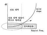
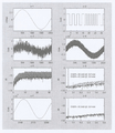
도 1(a)은 잡음 정형화 기술을 사용하여 신호대역의 잡음을 감소시키는 방법을 나타낸 도면이다.FIG. 1 (a) is a diagram illustrating a method of reducing noise in a signal band using a noise shaping technique.
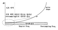
도 1(b)은 오버 샘플링 기술과 잡음 정형화 기술을 사용하여 신호대역의 잡음을 감소시키는 방법을 나타낸 도면이다.FIG. 1B is a diagram illustrating a method of reducing noise in a signal band using an oversampling technique and a noise shaping technique.
도 2는 델타 시그마 변조기를 사용하여 구현한 종래의 A/D 컨버터의 블록도이다.2 is a block diagram of a conventional A / D converter implemented using a delta sigma modulator.
도 3은 1비트 양자화기와 다중비트 양자화기를 사용하고 양자화 잡음을 아날로그 방식으로 정정하여 구현한 종래의 델타 시그마 변조기를 나타내는 도면이다.3 is a diagram illustrating a conventional delta sigma modulator using a 1-bit quantizer and a multi-bit quantizer, and implemented by correcting quantization noise in an analog manner.
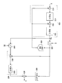
도 4는 1비트 양자화기와 다중비트 양자화기를 사용하여 구현한 본 발명의 제 1 실시예에 따른 델타 시그마 변조기를 나타내는 도면이다.4 is a diagram illustrating a delta sigma modulator according to a first embodiment of the present invention implemented using a 1-bit quantizer and a multi-bit quantizer.
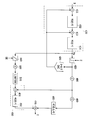
도 5는 1비트 양자화기와 다중비트 양자화기를 사용하여 구현한 본 발명의 제 2 실시예에 따른 델타 시그마 변조기를 나타내는 도면이다.5 is a diagram illustrating a delta sigma modulator according to a second embodiment of the present invention implemented using a 1-bit quantizer and a multi-bit quantizer.
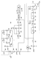
도 6은 도 5에 도시된 델타 시그마 변조기에 대해 구체적인 전달함수를 구하여 상세히 나타낸 도면이다.FIG. 6 is a diagram illustrating a detailed transfer function of the delta sigma modulator illustrated in FIG. 5.
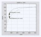
도 7은 본 발명에 따른 델타 시그마 변조기와 종래의 양자화 잡음 정정을 하 지 않은 델타 시그마 변조기에 대하여 오버 샘플링 비에 따른 신호 대 잡음비의 시뮬레이션 결과를 나타낸 도면이다.7 is a diagram illustrating a simulation result of signal-to-noise ratio according to oversampling ratio for a delta sigma modulator according to the present invention and a delta sigma modulator without conventional quantization noise correction.
도 8과 도 9는 본 발명에 따른 델타 시그마 변조기와 종래의 양자화 잡음 정정을 하지 않은 델타 시그마 변조기에 대한 매트랩(matlab) 시스템 시뮬레이션 결과를 나타내는 도면이다.8 and 9 are diagrams illustrating a matlab system simulation result for a delta sigma modulator according to the present invention and a delta sigma modulator without conventional quantization noise correction.
<도면의 주요부분에 대한 부호의 설명><Description of the symbols for the main parts of the drawings>
410 : 입력 적분회로 시리즈 411, 413, 451, 470 : 감산기410: input
412, 414 : 적분기 420 : 1 비트 양자화기412, 414: Integrator 420: 1-bit quantizer
430 : 1 비트 D/A 컨버터 440 : 다중 비트 양자화기430: 1-bit D / A converter 440: Multi-bit quantizer
450 : 에러 보정회로 460 : 지연소자450: error correction circuit 460: delay element
480, 490, 500 : 이득요소 510 : 리미터480, 490, 500: gain factor 510: limiter
본 발명은 델타 시그마 변조기에 관한 것으로, 특히 디지털 영역에서 에러를 정정함으로써 양자화 잡음을 감소시킬 수 있는 델타 시그마 변조기에 관한 것이다.The present invention relates to a delta sigma modulator, and more particularly to a delta sigma modulator capable of reducing quantization noise by correcting errors in the digital domain.
일반적으로, 낮은 주파수에서 동작하고 고정밀도의 해상도를 요구하는 특정 응용분야의 입출력단이나 송수신단에서는 델타 시그마 변조기(delta-sigma modulator)와 디지털 필터로 구성된 델타 시그마 A/D 컨버터 또는 델타 시그마 D/A 컨버터를 이용하여 신호변환을 한다. 델타 시그마 변조기는 오버 샘플링 기술과 잡 음 정형화(noise shaping) 기술을 사용한다. 도 1(a)에는 잡음 정형화 기술을 사용하여 신호대역의 잡음을 감소시키는 방법이 나타나 있고, 도 1(b)에는 오버 샘플링 기술과 잡음 정형화 기술을 사용하여 신호대역의 잡음을 감소시키는 방법이 나타나 있다. 잡음 정형화 기술은 신호변환시 발생하는 양자화 잡음을 사용하지 않는 신호대역으로 밀어내는 역할을 하고, 그 양은 델타 시그마 변조기의 차수에 따라 다르다. 오버 샘플링 기술은 모든 대역에서 일정한 양자화 잡음을 신호대역을 높여 실제 사용하는 신호대역에서는 양자화 잡음을 줄이는 기술이다. 또한, 델타 시그마 변조기는 고역통과 필터의 역할을 수행하고 오버 샘플링을 통해 신호대역을 높게 유지함으로써 작은 차수에서도 변환하려고 하는 신호대역의 잡음비는 상대적으로 작아져서 신호대역 내에서의 신호 대 잡음비를 향상시킬 수 있다. 즉, 델타 시그마 변조 방법은 잡음 정형화 기술과 오버 샘플링 기술을 이용하여 사용하는 신호대역에서의 잡음을 줄여 고해상도를 얻을 수 있는 방법이다.In general, the delta sigma A / D converter or delta sigma D / S consisting of a delta-sigma modulator and a digital filter at the input / output or transmit end of certain applications that operate at low frequencies and require high resolution. Signal conversion using A converter. Delta sigma modulators use oversampling and noise shaping. FIG. 1 (a) shows a method for reducing noise in a signal band using a noise shaping technique, and FIG. 1 (b) shows a method for reducing noise in a signal band using an oversampling technique and a noise shaping technique. have. Noise shaping technology pushes the quantization noise that occurs during signal conversion into an unused signal band, the amount of which depends on the order of the delta sigma modulator. Oversampling is a technique in which the quantization noise is increased in all bands to reduce the quantization noise in the actual signal band. In addition, the delta sigma modulator acts as a highpass filter and keeps the signal band high through oversampling, so that the noise ratio of the signal band to be converted in a small order is relatively small to improve the signal-to-noise ratio within the signal band. Can be. In other words, the delta sigma modulation method is a method that can obtain a high resolution by reducing the noise in the signal band using a noise shaping technique and an oversampling technique.
도 2는 델타 시그마 변조기를 사용하여 구현한 종래의 A/D 컨버터의 블록도이다. 도 2의 A/D 컨버터의 특성은 오버 샘플링 비(oversampling ratio; OSR)가 일정한 경우에 아날로그 루프 필터의 차수(L)와 양자화기(quantizer)의 비트수(N)에 의해 결정된다. 일반적으로, 델타 시그마 변조기를 사용하여 구현한 A/D 컨버터에서는 양자화기의 비선형 특성을 피하기 위해 1 비트 양자화기를 사용한다. 그래서, 델타 시그마 변조기를 사용하여 구현된 A/D 컨버터는 1 비트 A/D 컨버터라고도 불린다. 일반적으로, 응용분야별로 요구되는 적절한 잡음비의 특성을 얻기 위하여 변조기의 차수(L)와 OSR 사이에는 반비례 관계가 성립된다. 예를 들어, 음성 주파수 대(voice band)(4 kHz, Fs = 8 kHz)의 응용에서는 L = 2, OSR = 256, N = 1이 적절하고, 가청 주파수대(audio band)(20 kHz, Fs = 44.1 kHz)의 응용에서는 L = 4, OSR = 64, N = 1이 적절하다. 여기서, Fs는 샘플링 주파수이다. L 값이 작음으로써 발생하는 특성의 열화는 OSR을 높임으로써 서로 상쇄할 수 있다.2 is a block diagram of a conventional A / D converter implemented using a delta sigma modulator. The characteristic of the A / D converter of FIG. 2 is determined by the order L of the analog loop filter and the number N of bits of the quantizer when the oversampling ratio (OSR) is constant. In general, an A / D converter implemented using a delta sigma modulator uses a 1-bit quantizer to avoid the nonlinear characteristics of the quantizer. Thus, an A / D converter implemented using a delta sigma modulator is also called a 1-bit A / D converter. In general, an inverse relationship is established between the order L of the modulator and the OSR to obtain the proper noise ratio characteristics required for the application. For example, in applications in the voice band (4 kHz, Fs = 8 kHz), L = 2, OSR = 256, N = 1 is appropriate, and audio band (20 kHz, Fs = 44.1 kHz), L = 4, OSR = 64, and N = 1 are appropriate. Where Fs is the sampling frequency. The deterioration of characteristics caused by the small L value can be canceled with each other by raising the OSR.
그런데, 오버 샘플링 기술은 Nyquist 주파수보다 OSR 만큼 높은 주파수에서 동작하므로 신호대역이 높은 응용에서는 회로로 구현하는 데 문제가 있다. 만일 Nyquist 주파수가 2 MHz인 응용에서 OSR이 256인 경우에는 동작주파수는 512 MHz가 되어 문제가 되고, OSR을 낮추기 위해서는 변조기의 차수(L)가 증가하기 때문에 회로로 구현했을 경우 잡음, 전력소모, 및 제품 단가(cost) 면에서 여러 가지 문제점이 나타난다. 특히, 아날로그 변조기의 경우에는 대부분의 회로가 잡음에 민감한 아날로그 회로로 구성되므로 잡음의 영향을 많이 받고 구현하기가 어렵다. However, since the oversampling technique operates at a frequency higher than the Nyquist frequency by OSR, there is a problem in implementing a circuit in an application having a high signal band. If the OSR is 256 in an application where the Nyquist frequency is 2 MHz, the operating frequency becomes 512 MHz, which is a problem.In order to lower the OSR, the order of the modulator (L) is increased, so the noise, power consumption, And various problems in terms of product cost. In particular, in the case of an analog modulator, since most circuits are composed of analog circuits which are sensitive to noise, they are difficult to implement under the influence of noise.
이러한 문제점을 해결하고자 최근에는 낮은 OSR과 변조기의 낮은 차수에서도 응용에 맞는 적절한 특성을 나타낼 수 있는 다양한 방식들이 제안되어 왔다. 이 제안들 중 중요한 방식으로 양자화 잡음을 각 단계(stage)별로 합산하고 이를 필터링하여 제거하는 다단 잡음정형(multi-stage noise shaping; MASH) 방식, 및 1 비트와 N 비트의 듀얼 양자화기를 사용하고 1 비트 양자화기에서 생기는 양자화 잡음을 아날로그 방식으로 제거하고 그 출력을 디지털 잡음 정형을 통하여 구현한 것을 예로 들 수 있다. 1 비트와 N 비트의 듀얼 양자화기를 사용한 후 디지털 정정을 사용하여 양자화 잡음을 제거하는 방식은 미국 등록특허 6,300,890호에 개시되어 있으며, 도 3에 도시되어 있다. 도 3에 도시된 종래의 델타 시그마 변조기는 1 비트 양 자화기를 포함하는 피드백 루프에 의해 아날로그 입력신호를 양자화할 수 있고, 다중 비트 양자화기(11)를 포함하는 루프를 사용하여 양자화 잡음 정정을 수행함으로써 양자화 잡음을 줄일 수 있는 것을 특징으로 한다. 도 3의 델타 시그마 변조기에서는 양자화 에러를 계산하기 위해 최종 단(final stage) 적분기(8)의 아날로그 출력신호에서 1 비트 D/A 컨버터(4)의 양자화된 아날로그 출력신호를 감산하여 1 비트 D/A 컨버터에서 생기는 양자화 잡음을 제거하게 된다. 그런데, 감산기(10)에서 감산하는 신호가 아날로그 신호이고 양자화 잡음을 제거하는 신호의 루프가 아날로그 회로이므로 잡음의 영향을 많이 받을 수 있다.In order to solve this problem, various methods have recently been proposed to exhibit proper characteristics even for low OSR and low order of modulator. An important method of these proposals is to use a multi-stage noise shaping (MASH) method that adds, filters, and removes quantization noise at each stage, and a dual quantizer of 1 and N bits. For example, the analog quantization noise generated from the bit quantizer is removed and the output is implemented through digital noise shaping. A method of removing quantization noise using digital correction after using a dual quantizer of 1 bit and N bits is disclosed in US Pat. No. 6,300,890 and shown in FIG. The conventional delta sigma modulator shown in FIG. 3 can quantize an analog input signal by a feedback loop comprising a 1 bit quantizer, and perform quantization noise correction using a loop comprising a
상술한 바와 같은 문제점을 해결하기 위하여, 본 발명에 따른 델타 시그마 변조기는 1 비트 양자화기와 다중 비트 양자화기와 에러 보정회로를 구비하고, 다중 비트 양자화기의 디지털 출력신호와 1 비트 양자화기의 디지털 출력신호를 사용하여 디지털 영역에서 에러를 정정함으로써 양자화 잡음을 감소시킬 수 있고 정정회로의 루프가 디지털 영역에서 이루어지므로 잡음에 대한 영향을 최소화할 수 있다. In order to solve the problems as described above, the delta sigma modulator according to the present invention includes a 1-bit quantizer, a multi-bit quantizer and an error correction circuit, and the digital output signal of the multi-bit quantizer and the digital output signal of the 1-bit quantizer By correcting the error in the digital domain, the quantization noise can be reduced, and the loop of the correction circuit is performed in the digital domain, thereby minimizing the influence on the noise.
본 발명의 목적은 양자화 잡음을 감소시키고 잡음의 영향을 최소화하는 델타 시그마 변조기를 제공하는 것이다.It is an object of the present invention to provide a delta sigma modulator that reduces quantization noise and minimizes the effects of noise.
본 발명의 다른 목적은 다중 비트 양자화기에 의해 발생할 수 있는 DC 옵셋을 제거할 수 있는 델타 시그마 변조기를 제공하는 것이다.It is another object of the present invention to provide a delta sigma modulator that can eliminate the DC offset that may be caused by a multi-bit quantizer.
본 발명에 따른 델타 시그마 변조기는 1 비트 양자화기와 다중 비트 양자화기와 에러 보정회로를 구비하고 상기 다중 비트 양자화기의 디지털 출력신호와 상기 1 비트 양자화기의 디지털 출력신호를 사용하여 에러를 정정함으로써 아날로그 입력신호를 디지털 출력신호로 변환할 때 양자화 잡음을 정정하여 감소시키는 것을 특징으로 한다.The delta sigma modulator according to the present invention includes a 1-bit quantizer, a multi-bit quantizer, and an error correction circuit, and corrects an error using a digital output signal of the multi-bit quantizer and a digital output signal of the 1-bit quantizer. When the signal is converted into a digital output signal, the quantization noise is corrected and reduced.
본 발명에 따른 델타 시그마 변조기는 아날로그 입력신호가 입력되는 입력단자, 디지털 출력신호가 출력되는 출력단자, 상기 입력단자와 상기 출력단자 사이에 위치하고 인가되는 아날로그 신호를 양자화하고 양자화된 디지털 신호를 출력하기 위한 1 비트 양자화기, 상기 양자화된 디지털 신호를 양자화된 아날로그 신호로 변환시키는 1 비트 D/A 컨버터, 제 1 감산기와 상기 제 1 감산기의 출력을 적분하기 위한 적분기를 포함하는 하나 이상의 단계(stage)를 포함하고, 첫 번째 단계의 제 1 감산기는 상기 입력단자의 아날로그 입력신호에서 상기 1 비트 D/A 컨버터의 양자화된 아날로그 출력신호를 감산하고 마지막 단계의 적분기는 그 출력을 상기 1 비트 양자화기에 출력하는 입력 적분회로 시리즈, 상기 입력 적분회로 시리즈의 출력신호를 양자화하고 양자화된 디지털 신호를 출력하기 위한 다중 비트 양자화기, 상기 다중 비트 양자화기의 디지털 신호와 상기 1 비트 양자화기의 디지털 신호를 수신하여 에러를 보정하는 에러 보정회로, 상기 1 비트 양자화기의 양자화된 디지털 신호를 지연하기 위한 지연 소자, 및 상기 지연 소자의 출력신호에서 상기 에러 보정회로의 출력신호를 감산하고 그 결과를 출력하기 위한 제 2 감산기를 구비하는 것을 특징으로 한다.The delta sigma modulator according to the present invention quantizes an input terminal to which an analog input signal is input, an output terminal to which a digital output signal is output, quantizes an analog signal located between the input terminal and the output terminal, and outputs a quantized digital signal. One or more stages including a one bit quantizer for converting the quantized digital signal into a quantized analog signal, an integrator for integrating a first subtractor and an output of the first subtractor Wherein the first subtractor of the first stage subtracts the quantized analog output signal of the 1-bit D / A converter from the analog input signal of the input terminal and the last stage of integrator outputs its output to the 1-bit quantizer Quantize the output signal of the input integration circuit series, A multi-bit quantizer for outputting a magnetized digital signal, an error correction circuit for receiving a digital signal of the multi-bit quantizer and a digital signal of the 1-bit quantizer and correcting an error, and a quantized digital of the 1-bit quantizer And a second subtractor for subtracting the output signal of the error correction circuit from the output signal of the delay element and outputting the result.
상기 에러 보정회로는 상기 1 비트 양자화기의 디지털 신호에서 상기 다중 비트 양자화기의 디지털 신호를 감산하여 1 비트 양자화기에서 생기는 양자화 잡음과 다중비트 양자화기의 잡음의 상관관계를 구하기 위한 제 3 감산기, 및 상기 제 3 감산기의 출력신호를 미분하여 비트 양자화기에서 생기는 잡음량에 대하여 고역통과 필터의 기능을 구현함으로써 원하는 신호대역에서의 잡음량을 최소화하는 잡음 정형을 위한 미분기를 포함하는 것을 특징으로 한다.The error correction circuit may further include: a third subtractor for subtracting the digital signal of the multi-bit quantizer from the digital signal of the 1-bit quantizer to obtain a correlation between quantization noise generated in the 1-bit quantizer and noise of the multi-bit quantizer; And a differentiator for noise shaping to minimize the amount of noise in a desired signal band by differentiating the output signal of the third subtractor to implement a function of a high pass filter with respect to the amount of noise generated in the bit quantizer. .
상기 델타 시그마 변조기는 상기 다중 비트 양자화기와 상기 에러 보정회로 사이에 리미터를 더 구비하여 다중비트 양자화기를 사용하여 생길 수 있는 DC 옵셋을 제거하는 기능을 추가한 것을 특징으로 한다. The delta sigma modulator further includes a limiter between the multi-bit quantizer and the error correction circuit to remove a DC offset that may be generated by using the multi-bit quantizer.
이하, 첨부된 도면을 참조하여 본 발명에 따른 델타 시그마 변조기에 대해 설명한다.Hereinafter, a delta sigma modulator according to the present invention will be described with reference to the accompanying drawings.
도 4는 1비트 양자화기와 다중비트 양자화기를 사용하여 구현한 본 발명의 제 1 실시예에 따른 델타 시그마 변조기를 나타내는 도면이다.4 is a diagram illustrating a delta sigma modulator according to a first embodiment of the present invention implemented using a 1-bit quantizer and a multi-bit quantizer.
도 4의 델타 시그마 변조기는 아날로그 입력신호(X)가 입력되는 입력단자, 디지털 출력신호(Y)가 출력되는 출력단자, 입력단자와 출력단자 사이에 위치하고 인가되는 아날로그 신호를 양자화하고 양자화된 디지털 신호를 출력하기 위한 1 비트 양자화기(420), 양자화된 디지털 신호를 양자화된 아날로그 신호로 변환시키는 1 비트 D/A 컨버터(430), 감산기와 적분기를 포함하는 하나 이상의 단계(stage)를 포함하고 아날로그 입력신호(X)에서 1 비트 D/A 컨버터(430)의 양자화된 아날로그 출력신호를 감산하고 적분하여 그 출력을 1 비트 양자화기(420)에 출력하는 입력 적분회로 시리즈(410), 입력 적분회로 시리즈(410)의 출력신호를 양자화하고 양자화된 디지털 신호를 출력하기 위한 다중 비트 양자화기(440), 다중 비트 양자화기(440)의 디지털 출력신호와 1 비트 양자화기(420)의 디지털 출력신호를 수신하여 에러를 보정하는 에러 보정회로(450), 1 비트 양자화기(420)의 양자화된 디지털 신호를 지연하기 위한 지연 소자(460), 및 지연 소자(460)의 출력신호에서 에러 보정회로(450)의 출력신호를 감산하고 감산결과를 출력하기 위한 감산기(470)를 구비한다.The delta sigma modulator of FIG. 4 quantizes the quantized and quantized analog signal which is located between the input terminal to which the analog input signal X is input, the output terminal to which the digital output signal Y is output, and between the input terminal and the output terminal. A one
입력 적분회로 시리즈(410)는 아날로그 입력신호에서 1 비트 D/A 컨버터(430)의 아날로그 출력신호를 감산하는 감산기(411), 감산기(411)의 출력신호를 적분하는 적분기(412), 적분기(412)의 출력신호에서 1 비트 D/A 컨버터(430)의 아날로그 출력신호를 감산하는 감산기(413), 및 감산기(413)의 출력신호를 적분하는 적분기(414)를 포함한다.The input
에러 보정회로(450)는 1 비트 양자화기(420)의 디지털 출력신호에서 다중 비트 양자화기(440)의 디지털 출력신호를 감산하여 1 비트 양자화기에서 생기는 양자화 잡음과 다중 비트 양자화기의 잡음과의 상관관계를 구하기 위한 감산기(451), 및 감산기(451)의 출력신호를 미분하여 비트 양자화기에서 생기는 잡음량에 대하여 고역통과 필터의 기능을 구현함으로써 원하는 신호대역에서의 잡음량을 최소화하는 미분기(452)를 포함한다.The
이하, 도 4를 참조하여 본 발명의 제 1 실시예에 따른 델타 시그마 변조기의 동작에 대해 설명한다.Hereinafter, the operation of the delta sigma modulator according to the first embodiment of the present invention will be described with reference to FIG. 4.
도 4에서 입력 적분회로 시리즈(410)는 감산기와 적분기로 구성된 하나 이상의 단계로 구성되며, 도 4에는 2 단계로 구성된 2차의 경우에 대해 나타내었다. 아날로그 입력신호(X)는 1 비트 양자화기(420)에 의해 양자화되어 디지털 신호로 변환된다. 1 비트 양자화기(420)와 1 비트 D/A 컨버터(430)와 감산기들(411, 413)과 적분기들(412, 414)로 이루어진 피드백 루프에 의해 잡음이 원하는 신호대역 밖으로 정형되어 원하는 신호 내에서는 상대적으로 잡음이 적게 되고, 아날로그 입력신호는 계속하여 양자화가 진행된다. 양자화하는 과정에서 양자화 잡음(E)이 섞일 수 있으므로 1 비트 양자화기(420)의 출력신호는 양자화 잡음(E)을 포함하는 신호가 된다. 다중 비트 양자화기(440)는 입력 적분회로 시리즈(410)의 출력신호, 즉 1 비트 양자화기(420)의 입력신호(Vm)를 수신하고 양자화된 디지털 신호를 출력한다. 1 비트 양자화기(420)와 마찬가지로 다중 비트 양자화기(440)에서도 양자화하는 과정에서 양자화 잡음(EE)이 섞일 수 있으므로 다중 비트 양자화기(440)의 출력신호는 양자화 잡음(E)을 포함하는 신호가 된다. 에러 보정회로(450)의 감산기(451)는 1 비트 양자화기(420)의 출력신호에서 다중 비트 양자화기(440)의 출력신호를 감산하고, 미분기(452)는 그 결과를 미분한다. 지연소자(460)는 1 비트 양자화기(420)의 출력신호를 수신하여 일정시간 지연시키는 기능을 한다. 감산기(470)는 지연소자(460)의 출력신호에서 에러 보정회로(450)의 출력신호를 감산하여 출력단자에 출력신호(Y)를 발생시킨다. 이러한 과정에서 감산기(451)는 각 비트 양자화기에서 생기는 양자화 잡음의 상관관계를 구하고 미분기(452)는 각 비트 양자화기에서 생기는 잡음량에 대하여 고역통과 필터의 기능을 구현함으로써 원하는 신호대역에서의 잡음량을 최소화하는 잡음 정형의 기능을 한다. 결국 최종 출력단에서는 상대적으로 큰 1 비트 양자화기 잡음은 제거되고 상대적으로 작은 다중비트 양자화기의 잡음은 미분기에 의한 잡음 정형(noise shaping)을 통하여 그 크기가 매우 작아지므로 신호 대 잡음비의 특성이 향상된다.In FIG. 4, the input integrating
도 5는 1비트 양자화기와 다중비트 양자화기를 사용하여 구현한 본 발명의 제 2 실시예에 따른 델타 시그마 변조기를 나타내는 도면으로서, 도 4에 도시된 본 발명의 제 1 실시예에 따른 델타 시그마 변조기에 각 단계의 이득의 차이를 보정하기 위한 소정의 이득요소와 리미터를 더 구비한다.FIG. 5 is a diagram illustrating a delta sigma modulator according to a second embodiment of the present invention implemented using a 1-bit quantizer and a multi-bit quantizer. The sigma modulator according to the first embodiment of the present invention shown in FIG. A predetermined gain element and limiter for correcting the difference in gain of each step are further provided.
도 5의 델타 시그마 변조기는 아날로그 입력신호(X)가 입력되는 입력단자, 디지털 출력신호(Y)가 출력되는 출력단자, 입력단자와 출력단자 사이에 위치하고 인가되는 아날로그 신호를 양자화하고 양자화된 디지털 신호를 출력하기 위한 1 비트 양자화기(420), 양자화된 디지털 신호를 양자화된 아날로그 신호로 변환시키는 1 비트 D/A 컨버터(430), 감산기와 적분기로 구성된 하나 이상의 단계(stage)를 포함하고 아날로그 입력신호(X)에서 1 비트 D/A 컨버터(430)의 양자화된 아날로그 출력신호를 감산하고 적분하여 그 출력을 1 비트 양자화기(420)에 출력하는 입력 적분회로 시리즈(410), 1 비트 양자화기(420)의 디지털 출력신호에 소정의 이득을 주기 위한 이득요소(480), 입력 적분회로 시리즈(410)의 출력신호를 양자화하고 양자화된 디지털 신호를 출력하기 위한 다중 비트 양자화기(440), 다중 비트 양자화기(440)의 디지털 출력신호에 소정의 이득을 주기 위한 이득요소(500), 이득요소(500)의 출력신호를 안정화시키는 리미터(510), 리미터(510)의 출력신호와 이 득요소(480)의 출력신호를 수신하여 에러를 보정하는 에러 보정회로(450), 이득요소(480)의 출력신호에 소정의 이득을 주기 위한 이득요소(490), 이득요소(490)의 출력신호를 지연하기 위한 지연 소자(460), 및 지연 소자(460)의 출력신호에서 에러 보정회로(450)의 출력신호를 감산하고 감산결과를 출력하기 위한 감산기(470)를 구비한다.The delta sigma modulator of FIG. 5 quantizes an input signal to which an analog input signal X is input, an output terminal to which a digital output signal Y is output, an analog signal located between an input terminal and an output terminal, and quantizes the quantized digital signal. A one-
입력 적분회로 시리즈(410)는 아날로그 입력신호에서 1 비트 D/A 컨버터(430)의 아날로그 출력신호를 감산하는 감산기(411), 감산기(411)의 출력신호를 적분하는 적분기(412), 적분기(412)의 출력신호에서 1 비트 D/A 컨버터(430)의 아날로그 출력신호를 감산하는 감산기(413), 및 감산기(413)의 출력신호를 적분하는 적분기(414)를 포함한다.The input
에러 보정회로(450)는 이득요소(480)의 출력신호에서 리미터(510)의 출력신호를 감산하는 감산기(451), 및 감산기(451)의 출력신호를 미분하는 미분기(452)를 포함한다.The
도 5에 도시된 본 발명의 제 2 실시예에 따른 델타 시그마 변조기는 각 단계의 이득의 차이를 서로 보정하기 위한 소정의 이득요소와 다중 비트 양자화기를 사용함으로써 생길 수 있는 DC 옵셋을 제거하기 위하여 다중 비트 양자화기의 출력을 일정한 레벨로 제한하는 리미터를 더 구비하고 있다는 점 외에는 도 4에 도시된 본 발명의 제 1 실시예에 따른 델타 시그마 변조기와 동일하므로 여기서 그 설명을 생략한다.The delta sigma modulator according to the second embodiment of the present invention shown in Fig. 5 is designed to remove a DC offset that may be generated by using a multi-bit quantizer and a predetermined gain element for correcting each other's gain difference. Except that it further includes a limiter for limiting the output of the bit quantizer to a constant level, the description thereof is omitted here because it is the same as the delta sigma modulator according to the first embodiment of the present invention shown in FIG.
도 6은 도 5에 도시된 2차의 델타 시그마 변조기에 대해 구체적으로 전달함 수를 구하여 상세히 나타낸 도면이다. FIG. 6 is a diagram illustrating in detail the transfer function of the second delta sigma modulator illustrated in FIG. 5.
도 6에서 참조번호 410은 입력 적분회로 시리즈(410)를, 참조번호 420은 1 비트 양자화기를, 참조번호 430은 1 비트 D/A 컨버터를, 참조번호 440은 다중 비트 양자화기를, 참조번호 450은 에러 보정회로를, 참조번호 460은 지연회로를, 참조번호 470은 감산기를, 참조번호 480과 490과 500은 이득요소를, 510은 리미터를 각각 나타내며, 설명의 편의를 위해서 이들 참조번호들은 도 5에서와 동일한 번호를 사용하였다. 도 6에서 이득요소 옆에 놓인 수치들(a1 = 1, a2 = 1, a3 = 1, a4 = 0.75, a5 = -1.5, a6 = 1, b1 = 1, b4 = 1, b5 = -2, b6 = 1, c1 = 0.5, c2 = 0.5, g1 = 23, g2 = 210)은 본 발명의 실시예에서 사용한 전달함수의 계수 값을 나타낸다. In FIG. 6,
신호 전달함수와 잡음 전달함수를 합한 신호인 Y1(z)는 수학식 1과 같이 된다.Y1 (z), the sum of the signal transfer function and the noise transfer function, is expressed by
![]()
![]()
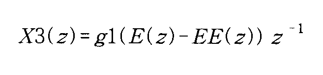
감산기(451)의 입력신호는 g1(X2 + E) - g1(X2 + EE) = g1(E - EE)이 된다. 다중 비트 양자화기(440)를 통과한 신호는 1 비트 양자화기에 비하여 상대적으로 작은 양자화 잡음(EE)을 가지고 있다. 도 6에 도시된 이득을 사용하여 계산하면 X3의 값은 수학식 2와 같다.The input signal of the
도 6의 델타 시그마 변조기의 피드백 루프에는 잡음 E가 존재하므로 출력 Y(z)= f(X(z), E(z), EE(z))가 된다. 이 함수 안에 있는 E를 제거하면 델타 시그마 변조기의 출력은 Y(z) = f(X(z), EE(z))가 된다. EE(z)는 상대적으로 에러의 양이 작은 다중 비트 양자화기(440)의 에러이다. 이렇게 함으로써 잡음특성에 가장 많은 영향을 줄 수 있는 잡음(E)를 제거하여 델타 시그마 변조기의 피드백 루프에 있는 에러의 영향은 제거할 수 있으므로 도 6에 도시된 델타 시그마 변조기는 잡음 특성이 우수하다.Since noise E exists in the feedback loop of the delta sigma modulator of FIG. 6, the output Y (z) = f (X (z), E (z), EE (z)). If we remove E inside this function, the output of the delta sigma modulator is Y (z) = f (X (z), EE (z)). EE (z) is an error of the
델타 시그마 변조기의 양자화 잡음 E를 제거하기 위해서는 출력신호(Y(z))는 수학식 3과 같이 되어야 한다.In order to remove the quantization noise E of the delta sigma modulator, the output signal Y (z) should be expressed by

수학식 1과 수학식 2를 사용하여 출력신호(Y(z))를 구하면 수학식 4와 같이 된다.Using equations (1) and (2), the output signal Y (z) is obtained as shown in equation (4).

수학식 4로부터 양자화 잡음 E는 상쇄되어 제거되고, 다중 비트 양자화기의 양자화 잡음 EE만 남아 있음을 알 수 있다. 또한, 수학식 4로부터 필요한 델타 시그마 변조기는 지연시간을 가지는 2차의 고역통과 필터를 포함하는 구조임을 알 수 있다. 고역통과 필터는 잡음(EE(z))을 원하는 대역 밖으로 밀어내고 원하는 신호대역 안에서는 적은 양의 잡음을 가질 수 있게 하는 잡음 정형의 특성을 가지고 있고, 이것은 곧 미분기라 볼 수 있다.It can be seen from
도 6에 도시된 바와 같은 본 발명의 델타 시그마 변조기는 원래의 신호의 손실은 없고 상대적으로 큰 양자화 잡음 E를 제거하고 상대적으로 작은 양자화 잡음 EE를 잡음 정형화(noise shaping)함으로써, 원하는 신호대역 내에서 우수한 신호 대 잡음비 특성을 가질 수 있다. 또한, 본 발명의 델타 시그마 변조기는 낮은 OSR에서도 디지털 영역에서 잡음소거(noise cancellation)를 함으로써 우수한 특성을 가질 수 있다. 도 6에서 이득(g1 및 g2)은 아날로그 신호가 디지털 신호로 넘어갈 때 신호를 비트로 산정하기 위한 것이므로 신호의 크기에만 영향을 미친다. 따라서, M 비트 이상의 신호 대 잡음비 특성을 위해서는 g1과 g2의 곱이 최소 2의 (M-1)승이 될 수 있도록 하여야 한다. 만일 14 비트 이상의 특성을 원한다면, g1 = 23이고 g2 = 210 이 되어야 한다. 그리고, 양자화 후에 에러 보정회로에서 연산을 수 행하기 위해 2의 보수형태로 연산을 진행하게 되는데, M 비트의 신호를 변환하려고 할 때 정상적인 경우라면 +(2M-1 - 1) ~ -(2M-1)의 범위에서 연산하여야 한다. 그런데, 이와 같이 연산하면 그 합이 0이 되지 않으므로 다중 비트 양자화기(440)의 출력단에 DC 값이 나타나게 된다. 이것을 방지하기 위해 다중 비트 양자화기(440)의 출력을 +(2M-1 - 1) ~ -(2M-1 - 1)로 제한하면 그 합을 0으로 만들 수 있다. 이러한 기능은 다중 비트 양자화기의 출력을 일정한 레벨로 제한하는 리미터(510)에 의해 수행된다.The delta sigma modulator of the present invention as shown in Fig. 6 eliminates the loss of the original signal, removes relatively large quantization noise E and noise shapings the relatively small quantization noise EE, thereby reducing the noise within the desired signal band. It can have excellent signal-to-noise ratio characteristics. In addition, the sigma delta sigma modulator of the present invention may have excellent characteristics by performing noise cancellation in the digital domain even at a low OSR. In FIG. 6, the gains g1 and g2 are used to calculate the signal in bits when the analog signal is transferred to the digital signal, and thus only affects the magnitude of the signal. Therefore, for the signal-to-noise ratio characteristic of M bits or more, the product of g1 and g2 must be a power of (M-1) of at least 2. If you want more than 14 bits, g1 = 2 3 and g2 = 2 10 . After the quantization, the operation is performed in two's complement form in order to perform the operation in the error correction circuit. If the signal is normal when the M bit signal is to be converted, it is + (2 M- 1-1) to-(2 M-1 ). However, since the sum does not become zero when the operation is performed, the DC value appears at the output terminal of the
상기에서는 간단한 2 차 시그마 델타 변조기를 예로 들어 설명하였다. 일반적으로 우수한 특성을 얻기 위해서 고차의 변조기를 사용하여 데이터 변환을 수행하는데, 이 경우에도 OSR과 변조기의 특성 사이에 비례관계가 성립한다. 그러므로 낮은 OSR에서는 좋은 특성이 나오지 않으므로 적절한 OSR을 유지해야 한다. 본 발명에서 제안된 회로 구조를 사용하면, 고차의 변조기에서도 상대적으로 큰 양자화 잡음을 제거하여 양자화 잡음 때문에 생기는 특성의 손실을 개선할 수 있다. 따라서, 본 발명에 따른 델타 시그마 변조기는 일반적인 A/D 변환기 또는 D/A 변환기에 적용할 수 있다. In the above, a simple second sigma delta modulator has been described as an example. In general, data conversion is performed using a higher-order modulator to obtain excellent characteristics. In this case, a proportional relationship is established between the OSR and the characteristics of the modulator. Therefore, a good OSR should be maintained because low OSR does not produce good characteristics. Using the circuit structure proposed in the present invention, it is possible to remove a relatively large quantization noise even in a higher-order modulator to improve the loss of characteristics caused by the quantization noise. Accordingly, the delta sigma modulator according to the present invention can be applied to a general A / D converter or a D / A converter.
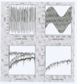
도 7은 본 발명에 따른 델타 시그마 변조기와 종래의 델타 시그마 변조기에 대하여 오버 샘플링 비에 따른 신호 대 잡음비의 시뮬레이션 결과를 나타낸 도면이다. 도 7에서 실선(solid line)은 본 발명의 회로구조를 이용하여 구현한 2 차 델타 시그마 변조기에 대한 시뮬레이션 결과를 나타내고, 점선(dotted line)은 종래 의 델타 시그마 변조기에 대한 시뮬레이션 결과를 나타낸다. 도 7에서 알 수 있듯이, 변조기의 차수에 적절한 OSR(Over-Sampling Ratio)을 가진 경우, 즉 도 7의 예에서 OSR이 256인 경우에는 본 발명의 변조기와 종래의 변조기는 특성의 차이가 거의 없으며, 이 값 이상의 경우에는 포화상태가 된다. 그러나, OSR이 낮은 경우, 예를 들면 도 7에서 OSR이 64인 경우에는, 본 발명의 변조기와 종래의 변조기는 15 dB 이상의 특성 차이가 있음을 알 수 있다. 즉, 동일한 차수의 변조기에서 동일한 OSR을 가지는 조건에서, 즉 포화상태의 조건이 아닌 충분한 변조기의 특성을 나타내는 상태에서, 본 발명의 변조기는 종래의 변조기에 비해 2.5 비트 이상 특성을 좋게 할 수 있다. 이것은 OSR을 2 배, 즉 128 까지 올려서 얻은 특성과 비슷한 특성의 향상이다. 다시 말하면, 본 발명의 변조기는 위와 같은 조건에서 동일차수에 대하여 종래의 변조기에 비해 OSR을 2 배정도 올린 효과를 나타낸다.7 is a diagram illustrating a simulation result of a signal-to-noise ratio according to an oversampling ratio for a delta sigma modulator according to the present invention and a conventional delta sigma modulator. In FIG. 7, a solid line represents a simulation result for the second delta sigma modulator implemented using the circuit structure of the present invention, and a dotted line represents a simulation result for a conventional delta sigma modulator. As can be seen in FIG. 7, when the OSR (Over-Sampling Ratio) is appropriate for the order of the modulator, that is, when the OSR is 256 in the example of FIG. 7, the modulator of the present invention and the conventional modulator have almost no difference in characteristics. If it is higher than this value, it will be saturated. However, when the OSR is low, for example, when the OSR is 64 in FIG. 7, it can be seen that the modulator of the present invention and the conventional modulator have a characteristic difference of 15 dB or more. That is, in the condition of having the same OSR in the same order modulator, i.e., in the state of exhibiting sufficient modulator characteristics other than the saturation condition, the modulator of the present invention can improve the characteristic of 2.5 bits or more as compared to the conventional modulator. This is a characteristic improvement similar to that obtained by doubling the OSR to 128. In other words, the modulator of the present invention exhibits the effect of raising the OSR by twice as much as the conventional modulator for the same order under the above conditions.
도 8과 도9는 본 발명에 따른 델타 시그마 변조기와 종래의 델타 시그마 변조기에 대한 매트랩(matlab) 시스템 시뮬레이션 결과를 나타내는 도면이다. 도 8과 도 9는 변조기의 차수가 2 차이고 OSR이 64인 경우에 대해 시뮬레이션한 결과를 나타낸다.8 and 9 are diagrams illustrating a matlab system simulation result for a delta sigma modulator according to the present invention and a conventional delta sigma modulator. 8 and 9 show simulation results for the case where the order of the modulator is 2 and OSR is 64. FIG.
도 8에서, (s-1)은 입력신호(-0.707 ~ +0.707)를 나타내고, (s-2)는 종래의 방식에 따른 변조기의 출력신호를 나타내며, (s-3)은 본 발명의 변조기에서 다중 비트 양자화기를 통과한 리미터의 출력신호(4 bit, -7 ~ +7)를 나타내고, (s-4)는 본 발명의 변조기의 출력신호(Y(z))를 나타내고, (s-5)는 본 발명에 따른 델타 시그마 변조기와 종래의 델타 시그마 변조기에 대하여 시뮬레이션 결과를 FFT한 결과 를 나타내고, (s-6)는 (s-5)의 결과를 신호대역폭(0.5)까지만 확대한 결과를 나타내고, (s-7)는 본 발명에 따른 델타 시그마 변조기의 출력을 4 차의 디지털 싱크 필터(Digital Sync Filter)에 넣어 출력을 16 다운샘플링(downsampling)한 결과를 나타내고, (s-8)는 디지털 싱크 필터의 결과를 FFT한 결과를 나타낸다.In FIG. 8, (s-1) represents an input signal (-0.707 to +0.707), (s-2) represents an output signal of a modulator according to the conventional scheme, and (s-3) represents a modulator of the present invention. Denotes the output signal (4 bit, -7 to +7) of the limiter passing through the multi-bit quantizer, (s-4) denotes the output signal (Y (z)) of the modulator of the present invention, and (s-5 ) Shows the result of FFT the simulation results for the delta sigma modulator according to the present invention and the conventional delta sigma modulator, and (s-6) shows the result of expanding the result of (s-5) only to the signal bandwidth (0.5). (S-7) shows the result of downsampling the output by inserting the output of the delta sigma modulator according to the present invention into a fourth order digital sync filter, and (s-8) The result of FFT of the result of a digital sync filter is shown.
(s-5)에서 위 부분은 본 발명의 델타 시그마 변조기에 대한 FFT 결과를 나타내고, 아래 부분은 종래의 델타 시그마 변조기에 대한 FFT 결과를 나타낸다. (s-6)에서 알 수 있듯이, (s-5)의 결과를 신호대역폭(0.5)까지만 확대한 결과 신호 대 잡음비 특성이 15 dB(2.5 bit) 좋아짐을 알 수 있다.In (s-5), the upper part shows the FFT result for the delta sigma modulator of the present invention, and the lower part shows the FFT result for the conventional delta sigma modulator. As can be seen from (s-6), as a result of expanding the result of (s-5) only to the signal bandwidth (0.5), it can be seen that the signal-to-noise ratio characteristic is improved by 15 dB (2.5 bit).
도 9에서, (s-9)는 본 발명의 델타 시그마 변조기의 1 비트 양자화기의 출력신호와 다중 비트 양자화기의 출력신호와의 에러 값의 차이를 구한 결과를 나타내고, (s-10)은 본 발명의 델타 시그마 변조기의 디지털 에러보정을 수행한 결과(Y2(z))를 나타내고, (s-11)은 (s-9)와 (s-10)에 대하여 FFT한 결과를 나타내고, (s-12)는 디지털 싱크 필터의 결과( 도8의 s-8의 결과) 파형을 나타낸다.In FIG. 9, (s-9) shows a result obtained by calculating an error value between the output signal of the 1-bit quantizer and the output signal of the multi-bit quantizer of the delta sigma modulator of the present invention. The digital error correction of the delta sigma modulator of the present invention is shown (Y2 (z)), (s-11) represents the result of FFT for (s-9) and (s-10), (s -12) shows a waveform of the result of the digital sync filter (result of s-8 in FIG. 8).
(s-11)에서 맨 위 파형은 (s-9)의 파형을 FFT한 결과를 나타내고, 중간의 파형은 (s-10)의 파형을 FFT한 결과를 나타내고, 맨 아래 파형은 본 발명의 델타 시그마 변조기의 최종 출력신호의 파형을 나타낸다. 맨 위의 파형은 잡음 정형화가 되지 않은 파형이며, 중간의 파형은 잡음 정형화가 된 파형이다. 델타 시그마 변조기의 특성에 영향을 많이 주는 양자화 잡음(E)은 에러보정에 의해 제거되고 나머지 양자화 잡음(EE)은 미분기에서 고역통과 필터링에 의해 제거된다.In (s-11), the top waveform shows the result of FFT the waveform of (s-9), the middle waveform shows the result of FFT the waveform of (s-10), and the bottom waveform shows the delta of the present invention. The waveform of the final output signal of the sigma modulator is shown. The top waveform is a waveform with no noise shaping, and the middle waveform is a waveform with noise shaping. Quantization noise (E), which greatly affects the characteristics of the delta sigma modulator, is removed by error correction and the remaining quantization noise (EE) is removed by highpass filtering in the differentiator.
상기에서는 본 발명의 바람직한 실시예를 참조하여 설명하였지만, 해당 기술 분야의 숙련된 당업자는 하기의 특허청구의 범위에 기재된 본 발명의 사상 및 영역으로부터 벗어나지 않는 범위 내에서 본 발명을 다양하게 수정 및 변경시킬 수 있음을 이해할 수 있을 것이다. Although described above with reference to a preferred embodiment of the present invention, those skilled in the art will be variously modified and changed within the scope of the invention without departing from the spirit and scope of the invention described in the claims below I can understand that you can.
상술한 바와 같이, 본 발명에 따른 델타 시그마 변조기에 의하면, 1 비트 양자화기와 다중 비트 양자화기와 에러 보정회로를 구비하고, 다중 비트 양자화기의 디지털 출력신호와 1 비트 양자화기의 디지털 출력신호를 사용하여 디지털 영역에서 에러를 정정함으로써 양자화 잡음을 감소시킬 수 있고 다중 비트 양자화기에 의해 발생할 수 있는 DC 옵셋을 제거할 수 있다. 또한, 본 발명에 따른 델타 시그마 변조기는 신호 대 잡음비의 향상을 이룰 수 있으며, 신호의 대역폭이 넓어져서 높은 OSR을 이룰 수 없는 경우와 고속동작에 대한 부담으로 고차의 구현이 어려운 산업분야의 응용에 사용되어 좋은 특성을 얻을 수 있다. As described above, the delta sigma modulator according to the present invention comprises a 1-bit quantizer, a multi-bit quantizer and an error correction circuit, and uses a digital output signal of the multi-bit quantizer and a digital output signal of the 1-bit quantizer. Correcting errors in the digital domain can reduce quantization noise and eliminate DC offsets that can be caused by multi-bit quantizers. In addition, the sigma delta sigma modulator according to the present invention can achieve an improved signal-to-noise ratio, which is difficult to achieve high OSR due to the wide bandwidth of the signal and high-speed operation. Can be used to obtain good characteristics.
Claims (10)
Priority Applications (3)
| Application Number | Priority Date | Filing Date | Title |
|---|---|---|---|
| KR1020030000354A KR100558481B1 (en) | 2003-01-03 | 2003-01-03 | Delta-sigma modulator that can reduce quantization noise |
| US10/723,159 US6922161B2 (en) | 2003-01-03 | 2003-11-26 | Delta-Sigma modulator for reducing quantization noise and oversampling ratio (OSR) |
| JP2003435973A JP3895325B2 (en) | 2003-01-03 | 2003-12-26 | Delta-sigma modulator |
Applications Claiming Priority (1)
| Application Number | Priority Date | Filing Date | Title |
|---|---|---|---|
| KR1020030000354A KR100558481B1 (en) | 2003-01-03 | 2003-01-03 | Delta-sigma modulator that can reduce quantization noise |
Publications (2)
| Publication Number | Publication Date |
|---|---|
| KR20040062823A KR20040062823A (en) | 2004-07-09 |
| KR100558481B1 true KR100558481B1 (en) | 2006-03-07 |
Family
ID=32677840
Family Applications (1)
| Application Number | Title | Priority Date | Filing Date |
|---|---|---|---|
| KR1020030000354A KR100558481B1 (en) | 2003-01-03 | 2003-01-03 | Delta-sigma modulator that can reduce quantization noise |
Country Status (3)
| Country | Link |
|---|---|
| US (1) | US6922161B2 (en) |
| JP (1) | JP3895325B2 (en) |
| KR (1) | KR100558481B1 (en) |
Families Citing this family (27)
| Publication number | Priority date | Publication date | Assignee | Title |
|---|---|---|---|---|
| US7212137B2 (en) * | 2003-10-09 | 2007-05-01 | Cirrus Logic, Inc. | Delta sigma modulator with integral decimation |
| JP4192900B2 (en) * | 2005-02-08 | 2008-12-10 | ソニー株式会社 | Quantization accuracy reproduction method, quantization accuracy reproduction device, imaging device, information processing device, and program |
| US20060217082A1 (en) * | 2005-03-22 | 2006-09-28 | Georg Fischer | Shaping noise in power amplifiers of duplex communication systems |
| KR100921498B1 (en) * | 2006-12-05 | 2009-10-13 | 한국전자통신연구원 | Delta Sigma modulator for multi-bit |
| US7545301B2 (en) | 2006-12-05 | 2009-06-09 | Electronics And Telecommunications Research Institute | Multi-bit delta-sigma modulator |
| US7622987B1 (en) | 2007-01-25 | 2009-11-24 | Pmc-Sierra, Inc. | Pattern-based DC offset correction |
| KR100861920B1 (en) * | 2007-05-10 | 2008-10-09 | 삼성전자주식회사 | Asymmetric-type pulse width modulation signal generator, and method thereof |
| US7659842B2 (en) * | 2007-10-24 | 2010-02-09 | Infineon Technologies Ag | Quantization error reduction in PWM full-MASH converters |
| JP5154659B2 (en) | 2007-12-19 | 2013-02-27 | エスティー‐エリクソン、ソシエテ、アノニム | Multi-bit sigma-delta modulator with reduced number of bits in the feedback path |
| US8223051B2 (en) * | 2008-01-14 | 2012-07-17 | Nxp, B.V. | Multi-bit sigma-delta modulator with reduced number of bits in feedback path |
| US8965726B2 (en) * | 2008-02-20 | 2015-02-24 | Robert Bosch Gmbh | System and method for measuring DC offset in a sensor output by modulating a signal-independent operating parameter of the sensor |
| US7782237B2 (en) * | 2008-06-13 | 2010-08-24 | The Board Of Trustees Of The Leland Stanford Junior University | Semiconductor sensor circuit arrangement |
| TWI427619B (en) * | 2008-07-21 | 2014-02-21 | Realtek Semiconductor Corp | Audio mixer and method thereof |
| US8629795B2 (en) | 2009-09-09 | 2014-01-14 | Taiwan Semiconductor Manufacturing Company, Ltd. | Micro-electro-mechanical systems (MEMS), systems, and operating methods thereof |
| JP5742815B2 (en) * | 2012-10-17 | 2015-07-01 | ソニー株式会社 | Noise canceling apparatus and noise canceling method |
| US8947285B2 (en) * | 2013-03-12 | 2015-02-03 | Infineon Technologies Ag | ADC with noise-shaping SAR |
| JP6228832B2 (en) * | 2013-12-17 | 2017-11-08 | ルネサスエレクトロニクス株式会社 | Delta-sigma modulator |
| KR102384362B1 (en) | 2015-07-17 | 2022-04-07 | 삼성전자주식회사 | Delta sigma modulator for shaping noise and audio codec having the same |
| KR101961363B1 (en) | 2017-07-06 | 2019-03-22 | 서강대학교산학협력단 | The second-order feed-forward delta-sigma modulator |
| US10892774B2 (en) * | 2017-09-29 | 2021-01-12 | Nagoya Institute Of Technology | Re-quantization device having noise shaping function, signal compression device having noise shaping function, and signal transmission device having noise shaping function |
| US9985646B1 (en) | 2017-10-18 | 2018-05-29 | Schweitzer Engineering Laboratories, Inc. | Analog-to-digital converter verification using quantization noise properties |
| US10033400B1 (en) | 2017-10-18 | 2018-07-24 | Schweitzer Engineering Laboratories, Inc. | Analog-to-digital converter verification using quantization noise properties |
| KR102326333B1 (en) | 2017-12-28 | 2021-11-15 | 한국전자통신연구원 | Method for signal modulation based on pulse density modulation and apparatus therefor |
| KR102118288B1 (en) * | 2019-03-29 | 2020-06-03 | 한양대학교 산학협력단 | A sigma-delta modulator for reducing clock-jitter and operation method thereof |
| CN113783572A (en) * | 2020-06-09 | 2021-12-10 | 上海新微技术研发中心有限公司 | Method for setting reverse gain coefficient in sigma-delta analog-to-digital converter |
| CN114124120B (en) * | 2021-10-12 | 2023-08-04 | 海德斯通信有限公司 | Receiver and communication device |
| CN115529043B (en) * | 2022-11-02 | 2023-03-24 | 南方电网数字电网研究院有限公司 | Multi-bit quantizer circuit, modulator and analog-to-digital converter |
Family Cites Families (11)
| Publication number | Priority date | Publication date | Assignee | Title |
|---|---|---|---|---|
| NL8101199A (en) * | 1981-03-12 | 1982-10-01 | Philips Nv | SYSTEM FOR QUANTIZING SIGNALS. |
| JPH01204528A (en) * | 1988-02-10 | 1989-08-17 | Fujitsu Ltd | A/d converter |
| US4862169A (en) * | 1988-03-25 | 1989-08-29 | Motorola, Inc. | Oversampled A/D converter using filtered, cascaded noise shaping modulators |
| US4876543A (en) * | 1988-05-31 | 1989-10-24 | Motorola, Inc. | Multi-rate cascaded noise shaping modulator |
| FI80548C (en) * | 1988-11-09 | 1990-06-11 | Nokia Oy Ab | Method for cascading two or more sigma-delta modulators and a sigma-delta modulator system |
| US5148167A (en) * | 1990-04-06 | 1992-09-15 | General Electric Company | Sigma-delta oversampled analog-to-digital converter network with chopper stabilization |
| US5030952A (en) * | 1990-12-26 | 1991-07-09 | Motorola, Inc. | Sigma-delta type analog to digital converter with trimmed output and feedback |
| EP0559944B1 (en) * | 1992-03-12 | 1996-02-28 | Siemens Aktiengesellschaft | Sigma-Delta-modulator |
| US5446460A (en) * | 1993-11-03 | 1995-08-29 | Advanced Micro Devices, Inc. | Fourth-order cascaded sigma-delta modulator |
| JP4357083B2 (en) * | 2000-06-01 | 2009-11-04 | 株式会社ルネサステクノロジ | Delta-sigma modulator and AD converter |
| TW584990B (en) * | 2001-05-25 | 2004-04-21 | Endpoints Technology Corp | Sigma-Delta modulation device |
-
2003
- 2003-01-03 KR KR1020030000354A patent/KR100558481B1/en not_active IP Right Cessation
- 2003-11-26 US US10/723,159 patent/US6922161B2/en not_active Expired - Fee Related
- 2003-12-26 JP JP2003435973A patent/JP3895325B2/en not_active Expired - Fee Related
Also Published As
| Publication number | Publication date |
|---|---|
| US6922161B2 (en) | 2005-07-26 |
| JP3895325B2 (en) | 2007-03-22 |
| KR20040062823A (en) | 2004-07-09 |
| JP2004215270A (en) | 2004-07-29 |
| US20040130471A1 (en) | 2004-07-08 |
Similar Documents
| Publication | Publication Date | Title |
|---|---|---|
| KR100558481B1 (en) | Delta-sigma modulator that can reduce quantization noise | |
| EP0704980B1 (en) | Analog-digital converter using Delta Sigma modulation | |
| US7190295B2 (en) | Accumulator for adaptive sigma-delta modulation | |
| JP3830924B2 (en) | Cascaded delta-sigma modulator | |
| EP2229734B1 (en) | A multi-bit sigma-delta modulator with reduced number of bits in feedback path | |
| JPH0797749B2 (en) | Delta-sigma modulation circuit of analog digital converter | |
| JPH0786951A (en) | Method and system of cascade-connecting three sigma-delta modulator | |
| JPH05110442A (en) | Method and constitution for stabilizing higher- order sigma/delta modulator | |
| JP2002076902A (en) | Multibit delta sigma ac converter | |
| US20080165043A1 (en) | Method and apparatus for A/D conversion | |
| US20040036636A1 (en) | Tone-free dithering methods for sigma-delta DAC | |
| WO2003043197A1 (en) | Sigma-delta modulation | |
| US20110267211A1 (en) | Analog-digital converter and operating method thereof | |
| KR100497702B1 (en) | Digital data converter | |
| JP3290314B2 (en) | Method for cascading three sigma-delta modulators and sigma-delta modulator system | |
| JP3785361B2 (en) | ΔΣ modulator, A / D converter and D / A converter | |
| JP4141865B2 (en) | Modulator | |
| JP3362718B2 (en) | Multi-bit-delta sigma AD converter | |
| KR102037610B1 (en) | Delta-Sigma ADC using SAR quantizer | |
| JPH04129334A (en) | Digital sigma-delta modulator | |
| EP1855384B1 (en) | Accumulator for adaptive sigma-delta modulation | |
| JPH11308110A (en) | Delta sigma type analog/digital converter | |
| JP3483000B2 (en) | ΔΣ modulator | |
| JP3047368B2 (en) | A / D converter circuit | |
| JPH0653836A (en) | Analog/digital conversion circuit |
Legal Events
| Date | Code | Title | Description |
|---|---|---|---|
| A201 | Request for examination | ||
| E902 | Notification of reason for refusal | ||
| E902 | Notification of reason for refusal | ||
| E701 | Decision to grant or registration of patent right | ||
| GRNT | Written decision to grant | ||
| FPAY | Annual fee payment |
Payment date: 20130131 Year of fee payment: 8 |
|
| FPAY | Annual fee payment |
Payment date: 20140129 Year of fee payment: 9 |
|
| LAPS | Lapse due to unpaid annual fee |