KR100196242B1 - Method of making a hybrid semiconductor structure and the semiconductor structure thereof - Google Patents
Method of making a hybrid semiconductor structure and the semiconductor structure thereof Download PDFInfo
- Publication number
- KR100196242B1 KR100196242B1 KR1019900004476A KR900004476A KR100196242B1 KR 100196242 B1 KR100196242 B1 KR 100196242B1 KR 1019900004476 A KR1019900004476 A KR 1019900004476A KR 900004476 A KR900004476 A KR 900004476A KR 100196242 B1 KR100196242 B1 KR 100196242B1
- Authority
- KR
- South Korea
- Prior art keywords
- substrate
- pads
- adhesive
- pad
- layer
- Prior art date
Links
Images


Classifications
-
- H—ELECTRICITY
- H01—ELECTRIC ELEMENTS
- H01L—SEMICONDUCTOR DEVICES NOT COVERED BY CLASS H10
- H01L23/00—Details of semiconductor or other solid state devices
- H01L23/48—Arrangements for conducting electric current to or from the solid state body in operation, e.g. leads, terminal arrangements ; Selection of materials therefor
-
- H—ELECTRICITY
- H01—ELECTRIC ELEMENTS
- H01L—SEMICONDUCTOR DEVICES NOT COVERED BY CLASS H10
- H01L24/00—Arrangements for connecting or disconnecting semiconductor or solid-state bodies; Methods or apparatus related thereto
- H01L24/80—Methods for connecting semiconductor or other solid state bodies using means for bonding being attached to, or being formed on, the surface to be connected
- H01L24/83—Methods for connecting semiconductor or other solid state bodies using means for bonding being attached to, or being formed on, the surface to be connected using a layer connector
-
- H—ELECTRICITY
- H01—ELECTRIC ELEMENTS
- H01L—SEMICONDUCTOR DEVICES NOT COVERED BY CLASS H10
- H01L21/00—Processes or apparatus adapted for the manufacture or treatment of semiconductor or solid state devices or of parts thereof
- H01L21/02—Manufacture or treatment of semiconductor devices or of parts thereof
- H01L21/04—Manufacture or treatment of semiconductor devices or of parts thereof the devices having at least one potential-jump barrier or surface barrier, e.g. PN junction, depletion layer or carrier concentration layer
- H01L21/50—Assembly of semiconductor devices using processes or apparatus not provided for in a single one of the subgroups H01L21/06 - H01L21/326, e.g. sealing of a cap to a base of a container
- H01L21/56—Encapsulations, e.g. encapsulation layers, coatings
- H01L21/563—Encapsulation of active face of flip-chip device, e.g. underfilling or underencapsulation of flip-chip, encapsulation preform on chip or mounting substrate
-
- H—ELECTRICITY
- H01—ELECTRIC ELEMENTS
- H01L—SEMICONDUCTOR DEVICES NOT COVERED BY CLASS H10
- H01L23/00—Details of semiconductor or other solid state devices
- H01L23/52—Arrangements for conducting electric current within the device in operation from one component to another, i.e. interconnections, e.g. wires, lead frames
- H01L23/522—Arrangements for conducting electric current within the device in operation from one component to another, i.e. interconnections, e.g. wires, lead frames including external interconnections consisting of a multilayer structure of conductive and insulating layers inseparably formed on the semiconductor body
- H01L23/532—Arrangements for conducting electric current within the device in operation from one component to another, i.e. interconnections, e.g. wires, lead frames including external interconnections consisting of a multilayer structure of conductive and insulating layers inseparably formed on the semiconductor body characterised by the materials
- H01L23/53204—Conductive materials
- H01L23/5328—Conductive materials containing conductive organic materials or pastes, e.g. conductive adhesives, inks
-
- H—ELECTRICITY
- H01—ELECTRIC ELEMENTS
- H01L—SEMICONDUCTOR DEVICES NOT COVERED BY CLASS H10
- H01L24/00—Arrangements for connecting or disconnecting semiconductor or solid-state bodies; Methods or apparatus related thereto
- H01L24/01—Means for bonding being attached to, or being formed on, the surface to be connected, e.g. chip-to-package, die-attach, "first-level" interconnects; Manufacturing methods related thereto
- H01L24/18—High density interconnect [HDI] connectors; Manufacturing methods related thereto
- H01L24/19—Manufacturing methods of high density interconnect preforms
-
- H—ELECTRICITY
- H01—ELECTRIC ELEMENTS
- H01L—SEMICONDUCTOR DEVICES NOT COVERED BY CLASS H10
- H01L24/00—Arrangements for connecting or disconnecting semiconductor or solid-state bodies; Methods or apparatus related thereto
- H01L24/01—Means for bonding being attached to, or being formed on, the surface to be connected, e.g. chip-to-package, die-attach, "first-level" interconnects; Manufacturing methods related thereto
- H01L24/26—Layer connectors, e.g. plate connectors, solder or adhesive layers; Manufacturing methods related thereto
- H01L24/28—Structure, shape, material or disposition of the layer connectors prior to the connecting process
- H01L24/29—Structure, shape, material or disposition of the layer connectors prior to the connecting process of an individual layer connector
-
- H—ELECTRICITY
- H01—ELECTRIC ELEMENTS
- H01L—SEMICONDUCTOR DEVICES NOT COVERED BY CLASS H10
- H01L24/00—Arrangements for connecting or disconnecting semiconductor or solid-state bodies; Methods or apparatus related thereto
- H01L24/80—Methods for connecting semiconductor or other solid state bodies using means for bonding being attached to, or being formed on, the surface to be connected
- H01L24/81—Methods for connecting semiconductor or other solid state bodies using means for bonding being attached to, or being formed on, the surface to be connected using a bump connector
-
- H—ELECTRICITY
- H01—ELECTRIC ELEMENTS
- H01L—SEMICONDUCTOR DEVICES NOT COVERED BY CLASS H10
- H01L2224/00—Indexing scheme for arrangements for connecting or disconnecting semiconductor or solid-state bodies and methods related thereto as covered by H01L24/00
- H01L2224/01—Means for bonding being attached to, or being formed on, the surface to be connected, e.g. chip-to-package, die-attach, "first-level" interconnects; Manufacturing methods related thereto
- H01L2224/02—Bonding areas; Manufacturing methods related thereto
- H01L2224/023—Redistribution layers [RDL] for bonding areas
-
- H—ELECTRICITY
- H01—ELECTRIC ELEMENTS
- H01L—SEMICONDUCTOR DEVICES NOT COVERED BY CLASS H10
- H01L2224/00—Indexing scheme for arrangements for connecting or disconnecting semiconductor or solid-state bodies and methods related thereto as covered by H01L24/00
- H01L2224/01—Means for bonding being attached to, or being formed on, the surface to be connected, e.g. chip-to-package, die-attach, "first-level" interconnects; Manufacturing methods related thereto
- H01L2224/10—Bump connectors; Manufacturing methods related thereto
- H01L2224/12—Structure, shape, material or disposition of the bump connectors prior to the connecting process
- H01L2224/13—Structure, shape, material or disposition of the bump connectors prior to the connecting process of an individual bump connector
- H01L2224/13001—Core members of the bump connector
- H01L2224/13099—Material
- H01L2224/131—Material with a principal constituent of the material being a metal or a metalloid, e.g. boron [B], silicon [Si], germanium [Ge], arsenic [As], antimony [Sb], tellurium [Te] and polonium [Po], and alloys thereof
- H01L2224/13101—Material with a principal constituent of the material being a metal or a metalloid, e.g. boron [B], silicon [Si], germanium [Ge], arsenic [As], antimony [Sb], tellurium [Te] and polonium [Po], and alloys thereof the principal constituent melting at a temperature of less than 400°C
- H01L2224/13111—Tin [Sn] as principal constituent
-
- H—ELECTRICITY
- H01—ELECTRIC ELEMENTS
- H01L—SEMICONDUCTOR DEVICES NOT COVERED BY CLASS H10
- H01L2224/00—Indexing scheme for arrangements for connecting or disconnecting semiconductor or solid-state bodies and methods related thereto as covered by H01L24/00
- H01L2224/01—Means for bonding being attached to, or being formed on, the surface to be connected, e.g. chip-to-package, die-attach, "first-level" interconnects; Manufacturing methods related thereto
- H01L2224/10—Bump connectors; Manufacturing methods related thereto
- H01L2224/15—Structure, shape, material or disposition of the bump connectors after the connecting process
- H01L2224/16—Structure, shape, material or disposition of the bump connectors after the connecting process of an individual bump connector
- H01L2224/161—Disposition
- H01L2224/16151—Disposition the bump connector connecting between a semiconductor or solid-state body and an item not being a semiconductor or solid-state body, e.g. chip-to-substrate, chip-to-passive
- H01L2224/16221—Disposition the bump connector connecting between a semiconductor or solid-state body and an item not being a semiconductor or solid-state body, e.g. chip-to-substrate, chip-to-passive the body and the item being stacked
- H01L2224/16225—Disposition the bump connector connecting between a semiconductor or solid-state body and an item not being a semiconductor or solid-state body, e.g. chip-to-substrate, chip-to-passive the body and the item being stacked the item being non-metallic, e.g. insulating substrate with or without metallisation
-
- H—ELECTRICITY
- H01—ELECTRIC ELEMENTS
- H01L—SEMICONDUCTOR DEVICES NOT COVERED BY CLASS H10
- H01L2224/00—Indexing scheme for arrangements for connecting or disconnecting semiconductor or solid-state bodies and methods related thereto as covered by H01L24/00
- H01L2224/01—Means for bonding being attached to, or being formed on, the surface to be connected, e.g. chip-to-package, die-attach, "first-level" interconnects; Manufacturing methods related thereto
- H01L2224/26—Layer connectors, e.g. plate connectors, solder or adhesive layers; Manufacturing methods related thereto
- H01L2224/28—Structure, shape, material or disposition of the layer connectors prior to the connecting process
- H01L2224/29—Structure, shape, material or disposition of the layer connectors prior to the connecting process of an individual layer connector
- H01L2224/29001—Core members of the layer connector
- H01L2224/29099—Material
- H01L2224/291—Material with a principal constituent of the material being a metal or a metalloid, e.g. boron [B], silicon [Si], germanium [Ge], arsenic [As], antimony [Sb], tellurium [Te] and polonium [Po], and alloys thereof
- H01L2224/29101—Material with a principal constituent of the material being a metal or a metalloid, e.g. boron [B], silicon [Si], germanium [Ge], arsenic [As], antimony [Sb], tellurium [Te] and polonium [Po], and alloys thereof the principal constituent melting at a temperature of less than 400°C
-
- H—ELECTRICITY
- H01—ELECTRIC ELEMENTS
- H01L—SEMICONDUCTOR DEVICES NOT COVERED BY CLASS H10
- H01L2224/00—Indexing scheme for arrangements for connecting or disconnecting semiconductor or solid-state bodies and methods related thereto as covered by H01L24/00
- H01L2224/01—Means for bonding being attached to, or being formed on, the surface to be connected, e.g. chip-to-package, die-attach, "first-level" interconnects; Manufacturing methods related thereto
- H01L2224/26—Layer connectors, e.g. plate connectors, solder or adhesive layers; Manufacturing methods related thereto
- H01L2224/28—Structure, shape, material or disposition of the layer connectors prior to the connecting process
- H01L2224/29—Structure, shape, material or disposition of the layer connectors prior to the connecting process of an individual layer connector
- H01L2224/29001—Core members of the layer connector
- H01L2224/29099—Material
- H01L2224/2919—Material with a principal constituent of the material being a polymer, e.g. polyester, phenolic based polymer, epoxy
-
- H—ELECTRICITY
- H01—ELECTRIC ELEMENTS
- H01L—SEMICONDUCTOR DEVICES NOT COVERED BY CLASS H10
- H01L2224/00—Indexing scheme for arrangements for connecting or disconnecting semiconductor or solid-state bodies and methods related thereto as covered by H01L24/00
- H01L2224/01—Means for bonding being attached to, or being formed on, the surface to be connected, e.g. chip-to-package, die-attach, "first-level" interconnects; Manufacturing methods related thereto
- H01L2224/26—Layer connectors, e.g. plate connectors, solder or adhesive layers; Manufacturing methods related thereto
- H01L2224/28—Structure, shape, material or disposition of the layer connectors prior to the connecting process
- H01L2224/29—Structure, shape, material or disposition of the layer connectors prior to the connecting process of an individual layer connector
- H01L2224/29001—Core members of the layer connector
- H01L2224/29099—Material
- H01L2224/29198—Material with a principal constituent of the material being a combination of two or more materials in the form of a matrix with a filler, i.e. being a hybrid material, e.g. segmented structures, foams
- H01L2224/29298—Fillers
-
- H—ELECTRICITY
- H01—ELECTRIC ELEMENTS
- H01L—SEMICONDUCTOR DEVICES NOT COVERED BY CLASS H10
- H01L2224/00—Indexing scheme for arrangements for connecting or disconnecting semiconductor or solid-state bodies and methods related thereto as covered by H01L24/00
- H01L2224/73—Means for bonding being of different types provided for in two or more of groups H01L2224/10, H01L2224/18, H01L2224/26, H01L2224/34, H01L2224/42, H01L2224/50, H01L2224/63, H01L2224/71
- H01L2224/732—Location after the connecting process
- H01L2224/73201—Location after the connecting process on the same surface
- H01L2224/73203—Bump and layer connectors
-
- H—ELECTRICITY
- H01—ELECTRIC ELEMENTS
- H01L—SEMICONDUCTOR DEVICES NOT COVERED BY CLASS H10
- H01L2224/00—Indexing scheme for arrangements for connecting or disconnecting semiconductor or solid-state bodies and methods related thereto as covered by H01L24/00
- H01L2224/80—Methods for connecting semiconductor or other solid state bodies using means for bonding being attached to, or being formed on, the surface to be connected
- H01L2224/81—Methods for connecting semiconductor or other solid state bodies using means for bonding being attached to, or being formed on, the surface to be connected using a bump connector
- H01L2224/818—Bonding techniques
- H01L2224/81801—Soldering or alloying
-
- H—ELECTRICITY
- H01—ELECTRIC ELEMENTS
- H01L—SEMICONDUCTOR DEVICES NOT COVERED BY CLASS H10
- H01L2224/00—Indexing scheme for arrangements for connecting or disconnecting semiconductor or solid-state bodies and methods related thereto as covered by H01L24/00
- H01L2224/80—Methods for connecting semiconductor or other solid state bodies using means for bonding being attached to, or being formed on, the surface to be connected
- H01L2224/83—Methods for connecting semiconductor or other solid state bodies using means for bonding being attached to, or being formed on, the surface to be connected using a layer connector
- H01L2224/8319—Arrangement of the layer connectors prior to mounting
-
- H—ELECTRICITY
- H01—ELECTRIC ELEMENTS
- H01L—SEMICONDUCTOR DEVICES NOT COVERED BY CLASS H10
- H01L2224/00—Indexing scheme for arrangements for connecting or disconnecting semiconductor or solid-state bodies and methods related thereto as covered by H01L24/00
- H01L2224/80—Methods for connecting semiconductor or other solid state bodies using means for bonding being attached to, or being formed on, the surface to be connected
- H01L2224/83—Methods for connecting semiconductor or other solid state bodies using means for bonding being attached to, or being formed on, the surface to be connected using a layer connector
- H01L2224/838—Bonding techniques
-
- H—ELECTRICITY
- H01—ELECTRIC ELEMENTS
- H01L—SEMICONDUCTOR DEVICES NOT COVERED BY CLASS H10
- H01L2924/00—Indexing scheme for arrangements or methods for connecting or disconnecting semiconductor or solid-state bodies as covered by H01L24/00
- H01L2924/0001—Technical content checked by a classifier
- H01L2924/00011—Not relevant to the scope of the group, the symbol of which is combined with the symbol of this group
-
- H—ELECTRICITY
- H01—ELECTRIC ELEMENTS
- H01L—SEMICONDUCTOR DEVICES NOT COVERED BY CLASS H10
- H01L2924/00—Indexing scheme for arrangements or methods for connecting or disconnecting semiconductor or solid-state bodies as covered by H01L24/00
- H01L2924/0001—Technical content checked by a classifier
- H01L2924/00013—Fully indexed content
-
- H—ELECTRICITY
- H01—ELECTRIC ELEMENTS
- H01L—SEMICONDUCTOR DEVICES NOT COVERED BY CLASS H10
- H01L2924/00—Indexing scheme for arrangements or methods for connecting or disconnecting semiconductor or solid-state bodies as covered by H01L24/00
- H01L2924/01—Chemical elements
- H01L2924/01005—Boron [B]
-
- H—ELECTRICITY
- H01—ELECTRIC ELEMENTS
- H01L—SEMICONDUCTOR DEVICES NOT COVERED BY CLASS H10
- H01L2924/00—Indexing scheme for arrangements or methods for connecting or disconnecting semiconductor or solid-state bodies as covered by H01L24/00
- H01L2924/01—Chemical elements
- H01L2924/01006—Carbon [C]
-
- H—ELECTRICITY
- H01—ELECTRIC ELEMENTS
- H01L—SEMICONDUCTOR DEVICES NOT COVERED BY CLASS H10
- H01L2924/00—Indexing scheme for arrangements or methods for connecting or disconnecting semiconductor or solid-state bodies as covered by H01L24/00
- H01L2924/01—Chemical elements
- H01L2924/01013—Aluminum [Al]
-
- H—ELECTRICITY
- H01—ELECTRIC ELEMENTS
- H01L—SEMICONDUCTOR DEVICES NOT COVERED BY CLASS H10
- H01L2924/00—Indexing scheme for arrangements or methods for connecting or disconnecting semiconductor or solid-state bodies as covered by H01L24/00
- H01L2924/01—Chemical elements
- H01L2924/01033—Arsenic [As]
-
- H—ELECTRICITY
- H01—ELECTRIC ELEMENTS
- H01L—SEMICONDUCTOR DEVICES NOT COVERED BY CLASS H10
- H01L2924/00—Indexing scheme for arrangements or methods for connecting or disconnecting semiconductor or solid-state bodies as covered by H01L24/00
- H01L2924/01—Chemical elements
- H01L2924/01047—Silver [Ag]
-
- H—ELECTRICITY
- H01—ELECTRIC ELEMENTS
- H01L—SEMICONDUCTOR DEVICES NOT COVERED BY CLASS H10
- H01L2924/00—Indexing scheme for arrangements or methods for connecting or disconnecting semiconductor or solid-state bodies as covered by H01L24/00
- H01L2924/01—Chemical elements
- H01L2924/0105—Tin [Sn]
-
- H—ELECTRICITY
- H01—ELECTRIC ELEMENTS
- H01L—SEMICONDUCTOR DEVICES NOT COVERED BY CLASS H10
- H01L2924/00—Indexing scheme for arrangements or methods for connecting or disconnecting semiconductor or solid-state bodies as covered by H01L24/00
- H01L2924/01—Chemical elements
- H01L2924/01075—Rhenium [Re]
-
- H—ELECTRICITY
- H01—ELECTRIC ELEMENTS
- H01L—SEMICONDUCTOR DEVICES NOT COVERED BY CLASS H10
- H01L2924/00—Indexing scheme for arrangements or methods for connecting or disconnecting semiconductor or solid-state bodies as covered by H01L24/00
- H01L2924/01—Chemical elements
- H01L2924/01078—Platinum [Pt]
-
- H—ELECTRICITY
- H01—ELECTRIC ELEMENTS
- H01L—SEMICONDUCTOR DEVICES NOT COVERED BY CLASS H10
- H01L2924/00—Indexing scheme for arrangements or methods for connecting or disconnecting semiconductor or solid-state bodies as covered by H01L24/00
- H01L2924/01—Chemical elements
- H01L2924/01079—Gold [Au]
-
- H—ELECTRICITY
- H01—ELECTRIC ELEMENTS
- H01L—SEMICONDUCTOR DEVICES NOT COVERED BY CLASS H10
- H01L2924/00—Indexing scheme for arrangements or methods for connecting or disconnecting semiconductor or solid-state bodies as covered by H01L24/00
- H01L2924/01—Chemical elements
- H01L2924/01082—Lead [Pb]
-
- H—ELECTRICITY
- H01—ELECTRIC ELEMENTS
- H01L—SEMICONDUCTOR DEVICES NOT COVERED BY CLASS H10
- H01L2924/00—Indexing scheme for arrangements or methods for connecting or disconnecting semiconductor or solid-state bodies as covered by H01L24/00
- H01L2924/013—Alloys
- H01L2924/014—Solder alloys
-
- H—ELECTRICITY
- H01—ELECTRIC ELEMENTS
- H01L—SEMICONDUCTOR DEVICES NOT COVERED BY CLASS H10
- H01L2924/00—Indexing scheme for arrangements or methods for connecting or disconnecting semiconductor or solid-state bodies as covered by H01L24/00
- H01L2924/06—Polymers
- H01L2924/078—Adhesive characteristics other than chemical
- H01L2924/07802—Adhesive characteristics other than chemical not being an ohmic electrical conductor
-
- H—ELECTRICITY
- H01—ELECTRIC ELEMENTS
- H01L—SEMICONDUCTOR DEVICES NOT COVERED BY CLASS H10
- H01L2924/00—Indexing scheme for arrangements or methods for connecting or disconnecting semiconductor or solid-state bodies as covered by H01L24/00
- H01L2924/06—Polymers
- H01L2924/078—Adhesive characteristics other than chemical
- H01L2924/0781—Adhesive characteristics other than chemical being an ohmic electrical conductor
-
- H—ELECTRICITY
- H01—ELECTRIC ELEMENTS
- H01L—SEMICONDUCTOR DEVICES NOT COVERED BY CLASS H10
- H01L2924/00—Indexing scheme for arrangements or methods for connecting or disconnecting semiconductor or solid-state bodies as covered by H01L24/00
- H01L2924/095—Indexing scheme for arrangements or methods for connecting or disconnecting semiconductor or solid-state bodies as covered by H01L24/00 with a principal constituent of the material being a combination of two or more materials provided in the groups H01L2924/013 - H01L2924/0715
- H01L2924/097—Glass-ceramics, e.g. devitrified glass
- H01L2924/09701—Low temperature co-fired ceramic [LTCC]
-
- H—ELECTRICITY
- H01—ELECTRIC ELEMENTS
- H01L—SEMICONDUCTOR DEVICES NOT COVERED BY CLASS H10
- H01L2924/00—Indexing scheme for arrangements or methods for connecting or disconnecting semiconductor or solid-state bodies as covered by H01L24/00
- H01L2924/10—Details of semiconductor or other solid state devices to be connected
- H01L2924/11—Device type
- H01L2924/14—Integrated circuits
-
- H—ELECTRICITY
- H01—ELECTRIC ELEMENTS
- H01L—SEMICONDUCTOR DEVICES NOT COVERED BY CLASS H10
- H01L2924/00—Indexing scheme for arrangements or methods for connecting or disconnecting semiconductor or solid-state bodies as covered by H01L24/00
- H01L2924/15—Details of package parts other than the semiconductor or other solid state devices to be connected
- H01L2924/151—Die mounting substrate
- H01L2924/1517—Multilayer substrate
- H01L2924/15172—Fan-out arrangement of the internal vias
- H01L2924/15173—Fan-out arrangement of the internal vias in a single layer of the multilayer substrate
-
- H—ELECTRICITY
- H01—ELECTRIC ELEMENTS
- H01L—SEMICONDUCTOR DEVICES NOT COVERED BY CLASS H10
- H01L2924/00—Indexing scheme for arrangements or methods for connecting or disconnecting semiconductor or solid-state bodies as covered by H01L24/00
- H01L2924/15—Details of package parts other than the semiconductor or other solid state devices to be connected
- H01L2924/151—Die mounting substrate
- H01L2924/156—Material
- H01L2924/15786—Material with a principal constituent of the material being a non metallic, non metalloid inorganic material
- H01L2924/15787—Ceramics, e.g. crystalline carbides, nitrides or oxides
-
- H—ELECTRICITY
- H01—ELECTRIC ELEMENTS
- H01L—SEMICONDUCTOR DEVICES NOT COVERED BY CLASS H10
- H01L2924/00—Indexing scheme for arrangements or methods for connecting or disconnecting semiconductor or solid-state bodies as covered by H01L24/00
- H01L2924/19—Details of hybrid assemblies other than the semiconductor or other solid state devices to be connected
- H01L2924/1901—Structure
- H01L2924/1904—Component type
- H01L2924/19043—Component type being a resistor
-
- H—ELECTRICITY
- H01—ELECTRIC ELEMENTS
- H01L—SEMICONDUCTOR DEVICES NOT COVERED BY CLASS H10
- H01L2924/00—Indexing scheme for arrangements or methods for connecting or disconnecting semiconductor or solid-state bodies as covered by H01L24/00
- H01L2924/30—Technical effects
- H01L2924/301—Electrical effects
- H01L2924/30107—Inductance
-
- H—ELECTRICITY
- H01—ELECTRIC ELEMENTS
- H01L—SEMICONDUCTOR DEVICES NOT COVERED BY CLASS H10
- H01L2924/00—Indexing scheme for arrangements or methods for connecting or disconnecting semiconductor or solid-state bodies as covered by H01L24/00
- H01L2924/30—Technical effects
- H01L2924/301—Electrical effects
- H01L2924/3025—Electromagnetic shielding
Abstract
반도체 칩 또는 웨이퍼 기판(10)을 예를 들면 세라믹, 유리 등의 캐리어 플레이트 기판(11)에 부착하기 위하여, 기판들중 적어도 하나는 통상적으로는 패드가 위치된 곳 이외의 모든 영역내에 포토 마스킹 기술에 의해 노출된 점착성 재료로, 즉 전기적으로 절연성인 접착제로 코팅되어 재료를 경화시킨다. 이 후, 금속 분말(통상적으로 은)은 층의 잔류 점착성 부분으로 주입되어 전도성으로 되며, 두 기판은 정렬시 패드로 서로 대향하여 압착되고, 점착성 절연 재료 내의 금속 분말은 상기 패드 사이에 전기적 접속부를 형성한다. 절연층은 반도체 칩 또는 웨이퍼 기판 또는 캐리어 플레이트 기판중 한 기판 두 기판 모두에 제공된다. 기판들중 한 기판의 표면상에서의 패드와의 접속 라인은 경화된 전기적 절연층에 의해 도포된다. 표면 및 그 위의 접속 라인은 접착층의 제공 전에 패시베이트 되어 패드의 위치를 제외하고는 경화된다.In order to attach the semiconductor chip or wafer substrate 10 to a carrier plate substrate 11 such as, for example, ceramic, glass, at least one of the substrates is typically photomasked in all areas except where the pad is located. It is coated with a tacky material exposed by ie an electrically insulating adhesive to cure the material. Thereafter, the metal powder (usually silver) is injected into the remaining tacky portion of the layer to become conductive, and the two substrates are pressed against each other with pads in alignment, and the metal powder in the adhesive insulating material is connected to the electrical connection between the pads. Form. The insulating layer is provided on both the semiconductor chip or the wafer substrate or the carrier plate substrate. The connection line with the pad on the surface of one of the substrates is applied by a cured electrical insulating layer. The surface and the connection lines thereon are passivated prior to providing the adhesive layer and cured except for the location of the pads.
Description
제1도는 종래의 기술에 따라 플립-칩(flip-chip) 기술로 제조된 하이브 리드 회로(hybrid circuit)의 개략적인 단면도.1 is a schematic cross-sectional view of a hybrid circuit manufactured by flip-chip technology according to the prior art.
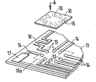
제2도는 캐리어 기판상에 반도체 칩을 피착하기 전의 분해 사시도.2 is an exploded perspective view before depositing a semiconductor chip on a carrier substrate.
제3도는 접속 패드에 금속화된 표면 영역을 구비한 캐리어 기판의 개략적인 수직 단면도.3 is a schematic vertical cross sectional view of a carrier substrate with a metallized surface area on the connection pad.
제4도는 접속 패드 또는 랜드(land)상에 금속화된 접착영역이 제공된 반도체 칩부의 수직 단면도.4 is a vertical cross-sectional view of a semiconductor chip portion provided with a metalized adhesive region on a connection pad or land.
제5도는 최종 압착 전에 접착층이 세라믹 기판에 피착된 하이브리드 회로의 구성을 도시한 단면도.5 is a cross-sectional view showing the configuration of a hybrid circuit in which an adhesive layer is deposited on a ceramic substrate before final pressing.
제6도는 최종 압착 전에 접착층이 반도체 칩에 피착된 제5도와 유사한 구성의 단면도.FIG. 6 is a cross-sectional view of a configuration similar to FIG. 5 in which an adhesive layer is deposited on a semiconductor chip prior to final compression.
* 도면의 주요부분에 대한 부호의 설명* Explanation of symbols for main parts of the drawings
10 : 반도체 칩 또는 웨이퍼 기판 11 : 캐리어 플레이트 기판10 semiconductor chip or
24 : 캐리어 접속 패드 14 : 외부접속라인24: carrier connection pad 14: external connection line
15 : 접속금속제 16 : 칩 접속 패드15: connection metal 16: chip connection pad
17 : 두꺼운 막 저항 18 : 얇은 막 저항17: thick membrane resistance 18: thin membrane resistance
20 : 베이스 영역 21 : 에미터 영역20: base area 21: emitter area
22 : 콜렉터 영역22: collector area
본 발명은 하이브리드 반도체 구조체를 제조하는 방법 및 이 방법에 의해 제조된 하이브리드 반도체에 관한 것으로, 특히 단자 또는 다른 접속 장치와의 접속 라인을 지지하는 캐리어 기판상의 유사한 접속 패드에 접속되는 접속 패드를 구비한 반도체 칩 및 그 제조 방법에 관한 것이다.The present invention relates to a method for manufacturing a hybrid semiconductor structure and to a hybrid semiconductor produced by the method, in particular having a connection pad connected to a similar connection pad on a carrier substrate supporting a connection line with a terminal or other connection device. A semiconductor chip and a method of manufacturing the same.
하이브리드 회로망을 플립-칩 기법으로 제작하는 것은 이미 제안되어 왔다. 이러한 기법은 금속 회로를 구비한 세라믹 기판 맞은편에 반도체 칩을 배치하고 칩의 패드와 기판 사이에 구형의 접촉 소자를 융해(fuse)시켜 칩을 기판에 접속시키는 것에 관한 것이다.(예로 McNutt 등에 의한 미국 특허 제 3,292,240호를 참조). 땜납은 일반적으로 작은 도트 형태인 납-주석의 소프트한 땜납이다.Fabrication of hybrid networks by flip-chip techniques has already been proposed. This technique involves placing a semiconductor chip across a ceramic substrate with a metal circuit and fusing a spherical contact element between the chip pad and the substrate to connect the chip to the substrate (e.g., by McNutt et al. US Pat. No. 3,292,240). Solder is a soft, tin-lead solder, usually in the form of small dots.
칩 또는 기판이 각각 서로 플립되어 있기 때문에 플립-칩기법이라 불리는 이러한 기술은 소형 금속 구체(tiny metaal spheres)또는 볼(balls)을 이용하지 않고 칩 및/또는 기판상의 각 접촉 소자에 소프트한 땜납층을 제공하며, 이미 제공된 땜납층을 이용하여 리플로우(reflow) 땜납 처리로 기판상에 칩을 땜납함으로서 개량되었다(이는 이께다(Ikeda)에 의한 미국 특허 제 3,517,279호에 설명되어 있다).Since the chips or substrates are flipped from each other, this technique, called flip-chip technique, uses a soft layer of solder on each contact element on the chip and / or substrate without the use of tiny metaal spheres or balls. It is improved by soldering a chip onto a substrate by reflow soldering using the solder layer already provided (which is described in US Pat. No. 3,517,279 to Ikeda).
Hymes 등에 의한 미국 특허 제 2,303,393호에는 단자 소자 또는 패드들이 고온 처리를 받더라도 기본적으로 변형되지 않는 점에 특징이 있는 것으로서, 미국 특허 제 2,292,240호 보다는 개량된 접속 방법 및 시스템이 개시되어 있다.U.S. Patent No. 2,303,393 to Hymes et al. Is characterized in that the terminal elements or pads do not fundamentally deform even when subjected to high temperature treatment, and an improved connection method and system is disclosed from U.S. Patent No. 2,292,240.
라인의 패킹 밀도(packing density)가 높은 경우, 인접 라인간에 쇼트됨이 없이 기계적 및 전기적으로 접속이 완전해야 하기 때문에 접속 장치를 제조하는데 어려움이 있다. 용융시 쇼트 회로가 되지 않게 전기적 접속이 양호하게 되도록 미소량의 소프트한 땜납을 반도체 칩의 접속 금속제 라인 및/또는 캐리어 기판의 패드에 제공하는데는 어려움이 있다. 따라서, 매우 작고 조밀한 공간의 전기적 접촉 금속제 영역을 구비한 반도체 소자들은 접속 라인 및 접속 패드의 기하학적 배치에 기초한 일부 제한을 통해 공지된 플립-칩 기법으로 접속될 수 있다.When the packing density of a line is high, it is difficult to manufacture a connection device because the connection must be complete mechanically and electrically without shorting between adjacent lines. It is difficult to provide a small amount of soft solder to the connection metal line of the semiconductor chip and / or the pad of the carrier substrate so that the electrical connection is good so that the short circuit does not become a short circuit during melting. Thus, semiconductor devices having very small and compact spaced electrically contact metal regions can be connected by known flip-chip techniques through some limitations based on the geometric arrangement of the connection lines and connection pads.
본 발명의 목적은 빠르고 신뢰할 수 있으며 부품들의 고 패킹 밀도를 가능하도록 기판상의 접속 패드에 칩상의 접속 패드를 접촉시키는 방법 및, 전기적 및 기계적으로 신뢰할 수 있으며 조밀한 공간의 전기적 접속을 가능케 하는 반도체-캐리어 기판 접속 구조체를 제공하는 방법에 관한 것이다.SUMMARY OF THE INVENTION An object of the present invention is a method of contacting a contact pad on a chip with a contact pad on a substrate so as to enable fast and reliable and high packing density of parts, and a semiconductor which enables electrical and mechanically reliable and compact electrical connection. A method for providing a carrier substrate connection structure.
요약하면, 예컨데 세라믹 같은 기판 캐리어 플레이트의 표면이 그 위에 접속패드를 갖는데, 예를 들면 직접 회로(IC) 같은 반도체 기판 칩은 칩의 표면 또는 내부의 적절한 전기 부품들과 접속될 수 있는 다수의 접속 패드를 갖고 있다.In summary, for example, the surface of a substrate carrier plate such as a ceramic has a connection pad thereon, for example, a semiconductor substrate chip such as an integrated circuit (IC) may be connected to a number of connections that can be connected with appropriate electrical components on or inside the chip. I have a pad.
본 발명에 따르면, 광-감지 전기적 절연 접착층이 반도체 칩의 표면 또는 기판 캐리어의 표면 또는 양 표면에 제공된다. 광-마스킹 기술에 의해 층을 전기적으로 절연시키는 접착층은 접속 패드가 없는 영역에서 경화된다. 그래서, 이 층은 접속 패드가 있는 영역에서는 노출되지 않으며 접착제 역할을 한다. 일반적으로 은 분말 또는 소정의 다른 적절한 확산가능한 금속인 금속 불말(a metal powder)은 상기 잔류 접착 영역 및 전기적으로 전도성인 재료에 제공되어 잔류 접착 영역이 전기적으로 전도성을 갖도록 한다. 전기적으로 전도성을 갖으며 그 위에 접착제가 코팅된 패드들은 서로 정렬(alignment)되어 대향하여 결합되므로, 한 기판 또는 다른 기판 또는 두 기판상의 각각의 패드 위에 있는 전기적으로 전도성인 접착 영역이 반대쪽 패드, 즉 전기적으로 전도성인 코팅부와 접속된다. 그래서, 반도체 기판 칩의 접속 패드는 기판 캐리어 플레이트, 통상적으로는 세라믹의 패드와 접착제에 의해 전기적 및 기계적으로 접속된다. 조립후에, 합성 구조체는 고온에서 경화된다. 본 발명의 특징에 따르면 최종 제품이 상기와 같이 이용되거나 또는 더 처리될 수도 있다.According to the present invention, a light-sensitive electrically insulating adhesive layer is provided on the surface of the semiconductor chip or the surface or both surfaces of the substrate carrier. The adhesive layer which electrically insulates the layer by the photo-masking technique is cured in the region where there is no connection pad. Thus, this layer is not exposed in the area where the connection pad is located and acts as an adhesive. A metal powder, generally silver powder or any other suitable diffuseable metal, is provided to the residual adhesive region and the electrically conductive material to make the residual adhesive region electrically conductive. The electrically conductive pads coated thereon with adhesives are aligned and bonded to each other so that the electrically conductive adhesive areas on one or the other or each pad on two substrates are opposite pads, i.e. It is connected with an electrically conductive coating. Thus, the connection pad of the semiconductor substrate chip is electrically and mechanically connected by a substrate carrier plate, usually a pad of ceramic and an adhesive. After assembly, the composite structure is cured at high temperature. According to a feature of the invention the final product may be used as such or further processed.
본 발명에 따른 방법은 고밀도 접속 패드 또는 라인을 구비한 반도체 칩이 결합 구조(geometry)에 관한 제한 없이 기판에 접속될 수 있다는 장점을 갖고 있다. 경화된 절연층은 접속 패드에서의 실제 접속부 이외의 소정의 노출된 금속 또는 반도체 표면의 절연을 제공한다.The method according to the invention has the advantage that semiconductor chips with high density connection pads or lines can be connected to the substrate without limitations on the coupling geometry. The cured insulating layer provides insulation of any exposed metal or semiconductor surface other than the actual connections at the connection pads.
본 발명의 특징에 따르면, 접속 패드는 보강될 수 있는데, 이러한 보강제로는 니켈 및/또는 은 또는 금으로 구성되어, 니켈 및/또는 은 또는 금의 보강층을 형성하는 것이 바람직하다. 상기 보강제는 볼록한 접촉 영역 때문에 접촉을 좀더 용이하게 해준다.According to a feature of the invention, the connection pad can be reinforced, which is preferably composed of nickel and / or silver or gold, forming a reinforcing layer of nickel and / or silver or gold. The reinforcing agent makes contact easier because of the convex contact area.
본 발명의 양호한 특징에 따르면, 접속 라인들이 기판 플레이트 또는 칩중 어느 한쪽 또는 양쪽에 배치될 때, 접속 라인들은 먼저 패시베이트(passivate)된다. 이 후, 광-감지 접착층은 각각의 기판 또는 칩상의 패시베이팅 층에 제공되어 경화되지만 패드상의 영역은 경화되지 않는다. 공지된 바와 같이, 광-마스크 기술은 경화되지 않고 남아있는 영역을 마스크하는데 이용된다. 금속 분말, 바람직하게는 은은 경화되지 않아 아직 접착성이 있는 영역으로 주입되고, 이 분말은 그 영역 내에 진동에 의해 분포된다. 그 결과 2중 절연층, 즉 패시베이팅 층 및 경화된 접착층을 구비한 캐리어 플레이트 또는 칩의 부조립체가 형성되지만 전도성의 패드 영역은 경화되지 않은 채로 남는다. 이후, 칩과 기판을 서로 대향되게 배치하여 정렬된 패드로 전기적 접속을 한다.According to a preferred feature of the invention, when the connection lines are arranged on either or both of the substrate plate or chip, the connection lines are first passivated. Thereafter, the light-sensitive adhesive layer is provided to the passivating layer on each substrate or chip to cure, but the area on the pad does not cure. As is known, photo-mask techniques are used to mask areas that remain uncured. The metal powder, preferably silver, is injected into an area that is not cured yet adhesive, and the powder is distributed by vibration in that area. The result is a subassembly of a carrier plate or chip with a double insulating layer, i.e. a passivating layer and a cured adhesive layer, but the conductive pad region remains uncured. Thereafter, the chip and the substrate are disposed to face each other to be electrically connected to the aligned pads.
조립 후, 제 1 단계에서의 고온 처리시 광-감지 접착층을 경화시키는데는 자외선이 적당하다.After assembly, ultraviolet light is suitable for curing the light-sensitive adhesive layer during the high temperature treatment in the first step.
본 시스템은 고밀도 및 최소 간격으로 서로 관련된 소자들이 정확한 위치를 갖도록 해준다. 자동 기계가 사용될 수 있는데, 20 마이크로미터 정도 또는 그보다 작은 간격으로 배열되도록 할 수 있다. 약 1㎛의 영역에서의 공차는 모놀리식 집적 반도체 회로와 연관되어 사용되는 포토-기술로 쉽게 얻어 질 수 있다. 노출되지 않은 패드 위의 접착부들을 제외하고 접착층 노출부는 약 1㎛ 또는 그보다 작은 정도의 공차를 이용할 수 있다. 접착 재료의 최소 오버랩을 얻을 수 있어서 접착 재료 또는 금속 분말이 퍼지는 위험성이 최소로 된다. 자동 위치화 장치로 캐리어 기판에 대한 반도체의 위치화시 공차를 20㎛보다 작게 유지시킬 수 있다. 캐리어 기판상의 패드 영역은 물론이고 반도체 칩의 접속 금속제 영역은 100㎛보다 작은 패드의 랜드의 중앙-대-중앙 간격을 기준으로 50㎛이하의 직격으로 감소시킬 수 있다.The system ensures that the devices associated with each other at high density and minimum spacing are positioned correctly. Automatic machines may be used, which may be arranged at intervals of about 20 micrometers or less. Tolerances in the region of about 1 μm can easily be obtained with photo-technology used in conjunction with monolithic integrated semiconductor circuits. Except for the adhesive portions on the unexposed pad, the adhesive layer exposed portion may utilize a tolerance of about 1 μm or less. A minimum overlap of the adhesive material can be obtained, thereby minimizing the risk of spreading the adhesive material or the metal powder. The automatic positioning device can maintain a tolerance of less than 20 μm in the positioning of the semiconductor with respect to the carrier substrate. The pad region on the carrier substrate as well as the connecting metal region of the semiconductor chip can be reduced to 50 mu m or less on the basis of the center-to-center spacing of the land of the pad smaller than 100 mu m.
경화되지 않은 접착부들이 서로 부착되도록, 즉 반대편 패드에 대향하여 부착되도록 칩들이 서로의 대향하여 배치된 후에, 칩의 전체 면이 기판면에 대향하여 압착된다. 그러므로, 패드에 전기적 접속부가 제공되고, 더불어 칩과 기판사이에 완전한 표면 접속부를 형성된다. 조합체를 클램프하거나 포트(pot)할 필요는 없으나, 유전 겔(gel)과 같은 패시베이션 겔을 전체 하이브리드 또는 합성 구조체를 보호하기 위해 제공하는 것이 바람직하다(이는 ICs제조와 관련된 공지된 표준 과정이다.).After the chips are placed opposite each other such that the uncured adhesives are attached to one another, ie opposite opposite pads, the entire surface of the chip is pressed against the substrate surface. Therefore, electrical connections are provided to the pads, and in addition, complete surface connections are formed between the chip and the substrate. It is not necessary to clamp or pot the combination, but it is desirable to provide a passivation gel, such as a dielectric gel, to protect the entire hybrid or synthetic structure (this is a well known standard procedure for making ICs). .
접착층은 전도성 입자들을 점착성 부분에 선택적으로 유지시키고 나머지 부분의 전도성 입자들의 피착을 방지하기 위하여 기판중 하나에만 경화되야 할 필요가 있다. 서로 결합될 플레이트들중 다른 하나(이는 기판 또는 칩일 수 있다)는 거의 경화되지 않게 남아 있어서, 패드 위에 금속 분말을 주입할 필요는 없다. 이는 제조 비용의 증가없이 실행될 수 있다. 칩 및 기판이 서로 대향하여 배치되면, 경화되지 않은 접착제는 경화된 접착제상에 부착되고, 소자들중 하나에 있는 패드 위의 금속 입자 또는 분말은 반대편의 경화되지 않은 부분으로 들어가 압착되어 전기적 접촉이 이루어진다.The adhesive layer needs to be cured only on one of the substrates to selectively retain the conductive particles in the tacky portion and to prevent deposition of the conductive particles in the remaining portions. The other one of the plates to be joined to one another (which may be a substrate or a chip) remains almost uncured, so it is not necessary to inject metal powder onto the pad. This can be done without increasing the manufacturing cost. When the chip and substrate are placed opposite each other, the uncured adhesive adheres onto the cured adhesive, and the metal particles or powder on the pads in one of the elements enter the opposite uncured portion and squeeze into electrical contact. Is done.
접착제의 적당한 두께는 약 5-10㎛ 이며, 입자 크기는 예로 직경이 1 내지 5 ㎛ 일 수 있다. 어떤 상황하에서는 패드 위의 입자 분산을 위해 진동을 이용하는 것이 바람직할 수 있지만 이것이 반드시 필요한 것은 아니다. 금속 분말의 분산을 위해서 진동보다는 오히려 원심력을 이용할 수 있다.The suitable thickness of the adhesive is about 5-10 μm, and the particle size may be, for example, 1-5 μm in diameter. Under some circumstances it may be desirable to use vibration to disperse particles on the pad, but this is not necessary. Centrifugal force rather than vibration can be used to disperse the metal powder.
기본적으로, 본 발명은 직경이 50㎛ 보다 작은 특정 전기적 접속 결합구조로 칩 및 기판의 전체 면을 상호 접속시키며 전체적으로 칩 및 기판의 양호한 열접촉 및 양호한 기계적 강도를 제공하도록 반도체 칩과 하이브리드 기판 사이에 미세 접착을 하기 위한 신기술을 제공한다. 이는 접속 패드의 영역에 정교하게 분포된 금속을 제공하여 선택적으로 전도성으로 되는 광-감지 접착 재료를 이용함으로써 성취된다.Basically, the present invention provides a specific electrical connection coupling structure having a diameter of less than 50 μm to interconnect the entire surface of the chip and the substrate and to provide good thermal contact and good mechanical strength of the chip and the substrate as a whole. New technology for fine adhesion is provided. This is accomplished by using a light-sensitive adhesive material that provides a finely distributed metal in the area of the connection pad, which becomes selectively conductive.
[실시예]EXAMPLE
제1도는 종래의 접속 시스템을 도시하고 있다(예로 미국 특허 제 3,292,240 및 제 3,303,393호 참조), 반도체 소자(10)는 기판 캐리어(11)에 금속 구체(12)로 된 접속부에 의해 접속된다. 반도체 칩(10)상의 접속 라인들(제1도에는 도시되어 있지 않음)은 구체(12 ; spheres)를 적당한 외부 또는 내부 전기 접속부에 접속시킨다. 제1도에 도시되어 있는 바와 같이, 용해 또는 땜납-접속된 후에, 구체(12)는 상기 반도체 소자(10)상의 접속 라인들(제1도에는 도시되지 않음)을 예를 들면 세라믹 재료로 만들어진 기판(11)상에 형성된 외부 접속 라인(14)에 접속시킨다. 금속 구체(12)는 납-주석의 소프트한 땜납제로 구성되며, 세라믹 기판(11)상의 외부 접속 라인(14)과 함께 반도체 칩(10)상의 각 접속 라인상의 납-주석의 소프트한 땜납제와 접속된다. 단부 또는 랜드(land)또는 패드(13)는 캐리어 또는 기판 플레이트(11)상에서 접속 패턴을 형성하는 외부 접속 라인(14)의 단자 영역을 형성한다.1 shows a conventional connection system (see, for example, US Pat. Nos. 3,292,240 and 3,303,393). The
본 발명에 따른 방법은 제2도를 살펴봄으로써 알 수 있는데, 본 도면은 반도체 칩 기판 소자(10)가 전기적 및 기계적으로 기판 플레이트(11)에 접속되기전의 하이브리드 회로 일부에 대한 분해도이다. 접속은 화살표 A 방향으로 이루어진다. 기판(11)상의 점선(1a)은 접속시 칩(10)이 배치되는 영역이다. 제1도에 도시된 바와 같이, 반도체 칩(10)은 그의 저면상에 다수의 접속 금속제(15)를 갖고 있다. 접속 금속제(15)는 패드 또는 랜드(16)에서 종단되고, 칩(10)상의 반도체소자에 대한 다른 접속부는 칩(10)의 하면에 있거나 또는 반도체 기술에서 널리 알려져 있듯이 칩(10)내에서 형성될 수 있다.The method according to the invention can be seen by looking at FIG. 2, which is an exploded view of a portion of the hybrid circuit before the semiconductor
패시베이션 층은 칩(10)의 저면에서 패드 또는 랜드(16)로부터 뻗어 있는 금속제(15)상에 배치될 수 있으나 칩(10)전체에 걸쳐서 패드 또는 랜드(16)는 노출된다. 마찬가지로, 캐리어 플레이트상의 랜드(13)는 그 위에 외부 접속 라인(14)과 접속된다. 외부 접속 라인(14)을 직접적인 전기적 접속체로 할 필요는 없으나 회로 소자를 구비할 수 있다. 예로서 도시된 기판 캐리어 플레이트(11)의 회로망에는 두꺼운 막 저항(17) 및 얇은 막 저항(18)이 예시되어 있다. 또한,, 저항(18)은 주파수에 의존하는 것으로 간주된다. 왜냐하면 칩이 저항-인덕턴스 소자로서 이용되기 때문이다. 제2도에 도시되어 있지 않은 패시베이션층은 랜드 또는 패드(13)는 노출시킨 채로 전체 접속 회로망 패턴(14,17,18)에 걸쳐서 배치된다.The passivation layer may be disposed on the
본 발명에 따르면, 반도체 칩 기판(10)상의 패드(16)와 캐리어기판(11)상의 패드(13)사이에 전기적 전도성 접속부를 형성하기 위하여, 전기적 비전도성 광-감지 접착층이 기판(11) 또는 칩(10)의 마주보는 면 위에 각각의 표면이 완전히 커버되도록 한다. 접속 패드의 영역에는 전기적으로 전도성인 재료가 주입된다. 전기적 전도성 재료가 있는 영역 이외에 접착층 영역이 경화되는데, 바람직하게는 공지되어 있는 표준형 포토-리소그라피 공정(후에 상세히 설명됨)을 이용하여 전기적 전도성 재료를 주입하기 전에 이루어진다.According to the present invention, in order to form an electrically conductive connection between the
반도체 칩(10)은 캐리어 플레이트(11)의 제2도의 점선(10a)으로 도시된 위치에 제공된다. 상기 접속시, 기계적 및 전기적 전도성 접착부는 기계적 분말 또는 삽입 재료에 의해 각각의 패드 위에서 전기적으로 전도성이 된 아직 경화되지 않은 접착제로 패드를 함께 부착시킴으로써 칩(10)의 접속 패드(16)와 기판(11)의 패드(13)사이에 형성된다.The
제3도는 2개의 인접 패드(13)를 가로지르는 제2도와 기판(11)를 통해 본 확대 단면도이다. 패시베이션 층(40)은 패드(13)의 표면을 제외한 전체 기판(11)위에 제공된다. 예로 알루미늄으로 이루어진 패드(13)의 표면은 단지 제한된 전기 전도성을 갖고 있다. 본 발명의 양호한 실시예에 따르면, 니켈 및/또는 은 또는 금의 보강 재료로 된 커버층(13')은 패드(13)위에 배치되어서 패시베이션 층(40) 위로 연장되어 보강재로서 제공된다. 이 후, 전기적 비전도성 광-감지 접착층(50)은 광-마스킹에 의해 패드(13)의 외측 영역에 노출된 전체 표면상에 보강 재료로 된 커버층(13')에 의해 보강되고 포토 마스킹에 의해 제공되어 경화된다. 패드(13) 상측에 있으며 노출되지 않은 접착층(50)의 영역(51)에는 접착제가 남아 있다. 전기적 전도성 재료는 상기 영역(51)내로 주입된다. 이로서 제3도에 개략적으로 도시된 바와 같이 영역(51)의 면적이 증가된다. 영역(51)은 전기적 전도성 재료의 주입으로 외부로 약간 볼록하게 튀어나와 전기적으로 전도체로 된다. 전기적 전도성 재료의 주입은, 예를 들면 분쇄된 은 등이 진동, 쉐이킹(shaking) 또는 원심력을 이용하여 처리될 수 있다. 금속 입자들은 점을 찍어 표시한 51'(제3도); 31'(제4도) 및 510, 310(제5도, 제6도)으로 도시되어 있다.3 is an enlarged cross sectional view through the
제4도는 집적 회로(IC) 반도체 칩(10)을 개략적으로 도시한 단면도이다. 제4도에 도시된 IC는 예시를 위한 것으로 플래너(IC)칩 기술로 만들어진 바이폴라 전력 트랜지스터이다. 본 발명은 설명된 바와 같으 반도체 소자를 구비한 하이브리드 회로에 제한되지 않으며, 예를 들면 참조된 미국 특허에 설명되어 있는 공지된 플립-칩 기술에 의해 기판에 부착되는 소정 형태의 IC 에 이용될 수도 있으며, 또한 반도체 소자들이 다수의 바람직하게는 정교하게 설계된 접속 구조를 갖는 접속 기판에 접속되는 임의의 회로에도 이용될 수 있다. 많은 조밀한 간격을 갖는 접속 금속제를 구비한 고집적 반도체 회로는 특히 본 발명을 적용하는데 적합하다.4 is a schematic cross-sectional view of an integrated circuit (IC)
제4도를 참조하면, 단결정 실리콘의 디스크-형 칩은 소정의 전도성 타입을 갖도록 도프된 기판(19)을 형성한다. 베이스 대역(20)은 기판 타입과 반대의 전도형을 갖는 기판 내로 확산된다. 기판과 동일한 전도성을 갖는 에미터 대역(21)은 베이스 대역 내로 확산된다. 링 형상의 콜렉터 확산 대역(22)은 기판내로 확산되어 링 형태로 베이스(20)를 둘러싸고 있다. 에미터 대역(21)은 콜렉터 대역(22)과 동시에 기판 내로 확산될 수 있다. 잘 알려져 있는 각 확산 처리로 기판(19)의 상측상에 실리콘 이산화물층(23)을 형성할 수 있다.Referring to FIG. 4, a disc-shaped chip of single crystal silicon forms a doped
베이스 대역(20)과 에미터 대역(21)은 접촉되어야 하기 때문에, 실리콘 이산화물층(23)은 베이스 및 에미터 각각에 접촉 창(24 및 25)을 형성하기 위해 에치된다.Since
콜렉터 확산 대역(22)을 접촉시키기 위한 부가적인 접촉 창들은 두개의 접촉 창(24,25)과는 다른 평면에 있기 때문에 제4도에서 생략하였다. 전도성 스트립망(conductive stripss)(26,27)은 패시베이션 층(23)의 표면에 제공된 후, 기판(19)의 표면 위에 형성된다.Additional contact windows for contacting the
제4도에 도시된 바와 같이, 전도 통로 또는 스트립(26)은 알루미늄으로 이루어져 베이스(20)와 접속되며, 알루미늄 스트립(27)은 에미터 대역(21)과 접속된다.As shown in FIG. 4, the conductive passages or strips 26 are made of aluminum and connected to the
전도 스트립(26)은 접촉 창(24)으로부터 통해 있으며, 패시베이션 실리콘 이산화물층(23)을 통하여 베이스 대역(20)의 외부 접속부를 형성하는 점까지 베이스 대역(20)과 결합된다. 이는 접속 패드 또는 랜드(26)에서 종단된다. 전도 스트립(27)은 접촉 창(25)으로부터 통해 있으며, 패시베이션 실리콘 이산화물층(23)을 통하여 에미터 대역(21)에 대한 외부 접속부를 형성하는 외부점까지 에미터 대역(21)과 결합된다. 외부 에미터 접속부에 대해서는 부가의 접속 금속제 랜드 또는 패드(16)에서 종단된다.The conducting
본 발명의 특징에 따르면, 패시베이션 층(28)은 접속 스트립(26,27)및 제 1 패시베이션 층(23)상에 제공되지만, 패드(16)는 노출된 상태로 남아 있다. 광-마스킹 기술은 접속 패드(16)가 위치해 있는 곳에 패시베이션 층(28)을 선택적으로 제공하기 위해 이용된다.According to a feature of the invention, the
패드(16)를 형성하는 접속 금속제의 표면은 제한된 전기적 전도율만을 갖고 있으며, 더욱 접속을 개선하기 위해 패시베이션 층(28)이 형성된 후 니켈 및/또는 은 또는 금의 보강 재료로 된 커버층(16')이 패드(16)에 제공되며, 보강 재료로 된 커버층(16')은 패시베이션 층(28)위로 연장된 접속 패드들을 보강해준다.The surface of the connecting metal forming the
본 발명의 특징에 따르면, 접착층(30)은 보강된 접속 패드(16,16')와 패시베이션 층(28)의 전체 면 위에 제공된다. 접속 금속제 패드(16,16')가 위치해 있는 부분에는 전기적 전도성 재료(31')가 주입된다. 전기적 전도성 재료를 주입, 바람직하게는 분말 또는 분쇄된 형태로 주입하면, 접속 패드(16)와 보강재료로 된 커버층(16')위의 접착층의 체적이 커져서, 제4도에 도시된 바와 같이 해당 영역이 바깥쪽으로 볼록하게 된다. 금속 분말은 점을 찍어 31'로 개략적으로 표시하였다.According to a feature of the invention, an
하이브리드 회로 제조법은 제5도 및 제6도를 참조한다.See FIG. 5 and FIG. 6 for hybrid circuit fabrication.
기판 플레이트(11)(제5도)은 제3도와 관련해 설명한 바와 같이, 회로망 패턴과, 접속 패드(13)가 없는 위치에 있는 패시베이션 층(40)을 구비하고 있다. 광- 감지 접착층(50)은 기판 플레이트(11)의 전체면, 즉 패시베이션 표면(40)과 외부 접속 라인(14) 및 패드 또는 랜드(13) 위에 제공된다. 다음 단계로서, 광-감지 표면(50)은 광-마스킹 기술을 이용해 노출되어 랜드 또는 패드(13)의 외부영역에서 경화되지만, 랜드 또는 패드(13) 위에서는 경화되지 않고 습한(moist)점착성 상태로 남는다. 이후, 국부적으로 경화되었지만 부분적으로 습한 층(50)은 분쇄된 전기적 전도성 재료, 바람직하게는 은을 구비하고 있는데, 상기 재료는 예를 들면 진동 또는 원심력을 부가적으로 이용해 패드(13) 상측의 영역에 부착 또는 상기 영역으로 침투된다. 이 후, 이와 같이 제작된 기판(11)위에는 반도체 소자(10)가 배치된다 .반도체 소자(10)는 제4도와 관련해 설명한 바와 마찬가지로, 전도 스트립(26,27)을 포함하며, 그 위에는 패시베이션 층(28)이 배치된다. 칩(10)은 반도체 소자(10)의 접속 패드(16)가 전기적 전도성 재료가 주입된 전도체로 구성된 기판(11)상의 패드(13)와 정렬되어 기판(11)에 대향하여 맞춰진다. 이 후, 전기적 접속부를 형성하는 접착 접속부가 또한 전도성 접속 영역(510)에 의해 패드(13)와 패드(16) 사이에 형성된다.The substrate plate 11 (FIG. 5) is provided with the network pattern and the
제5도는 칩(10)과 캐리어 기판(11) 사이의 공간을 확대하여 도시한다. 접착층(50)의 통상적인 두께는 마이크로미터 범위 내, 예컨대 약 5-10㎛ 정도의 두께이다. 전도성 접속 영역(510)에는 조립 전에 접착제를 침투할 필요는 없으나 남아있는 습한 표면에 달라붙어 조립중에 상기 영역에 압출될 수 있다. 조립시, 패시베이션 층(28)은 밀착된 구성이 형성되도록 접착층(50)에 대향하여 맞추어진다. 제5도는 공정을 보다 잘 예시하기 위해 조밀한 접속이 이루어지기 직전의 칩(10)에 대한 기판(11)의 위치를 도시한다.5 shows an enlarged view of the space between the
접착층을 캐리어 기판(11)에 꼭 제공할 필요는 없다. 제6도는 접착층(30)이 반도체(10) 위에 제공된 반대 과정을 도시한다(제4도 참조). 물론 접착층을 반도체(10)(제4도, 제6도) 위는 물론이고 캐리어 기판(11)(제3도,제5도) 위에 제공할 수도 있다.It is not necessary to provide the adhesive layer to the
제6도를 참조하면, 칩 또는 웨이퍼(10)(제4도)에는 전도성 회로망(26,27)및 패시베이션 층(28)과 함께 그 위에 제공된 광-감지 접착층(30)을 갖고 있다. 이후, 광-감지 층은 접속 금속제, 즉 패드(16) 외부 영역은 경과되지만 패드(16) 위에 재료가 침투가능한 습한 상태로 남아 있도록 하는 방식으로 광-마스킹 기술을 이용해 노출된다. 이 후, 전도 재료 통상적으로 분쇄된 은 재료는 접착층 위에 주입되어 패드 위의 여전히 습한 점착성의 접착제에 접착된다. 필요하다면, 분쇄된 은은 진동, 쉐이킹 또는 원심력과 같은 기계적 조작으로 층 내에 확산될 수 있다. 이 후, 이미 내부에 형성되어 있는 각 반도체 소자를 구비한 칩(10)은 원하는 바에 따라 개개의 소자로 분리될 수 있다.Referring to FIG. 6, the chip or wafer 10 (FIG. 4) has a
이 후, 이같이 제작된 반도체 칩(10)은 그 위에 패시베이션 층(40)을 구비한 기판(11)상에 배치되어(제5도 참조), 칩(10)으로부터의 접속 금속제 또는 패드(16)는 기판(11)의 금속제 또는 패드와 정렬된다. 전기적 및 기계적 접속부는 접착제에 의해 이루어지지만 (310)으로 도시된 전기적 접속부를 제공하기 위해 패드(13,16)의 영역 위에는 아직 접착제가 남아 있어 겨오하되지 않은 상태를 유지하고 있다.Thereafter, the thus produced
여러가지 변형 및 응용이 이루어질 수 있지만, 본 발명은 도면에 도시된 예나 특정 제조방법에 제한되지 않는다. 예를 들면, 패시베이션 층(28,40)은 포토리소그라피 공정에 의해 경화된 접착층(30,50)의 전기적으로 경화된 부분이 절연층으로 되어 패시베이션 층의 기능을 하기 때문에 엄밀하게는 꼭 필요하지 않다.Various modifications and applications may be made, but the invention is not limited to the examples shown in the drawings or the specific manufacturing method. For example, the passivation layers 28 and 40 are not strictly necessary because the electrically cured portions of the
보강 재료로 된 커버층(13',16')(제3도, 제4도)은, 특히 패드(13,16)가 접착제와 조화되고 각 접착층의 제공시 접착부로 될 수 있다면, 특히 상기 패드가 이미 니켈 및/또는 금으로 이루어져 있다면, 절대적으로 필요한 것은 아니다.Cover layers 13 ′, 16 ′ (FIGS. 3, 4) of the reinforcing material are especially suitable if the
캐리어 기판(11)용으로 적합한 재료로는 알루미늄 산화물(Al2O3) 또는 알루미늄 질화물(AIN)이 있지만, 유리나 실리콘 또한 사용될 수 있다. 만약 실리콘이 사용된다면, 기판(11)자체가 반도체 칩(10)과 유사한 반도체 소자일 수 있어, 본 발명의 방법으로 2개의 칩을 함께 동일하게 접속가능하게 된다. 따라서, 본 명세서에서 사용되는 기판이란 용어는 단지 부활성 또는 세라믹 기판을 의미하는 것이 아니라 다른 반도체 회로 부품 회로망 또는 IC 용 기판을 의미한다.Suitable materials for the
광-감지 접착층을 이용하며 그 일부만이 경화되도록 광-마스킹 기술을 이용해 그 특성을 제어함으로써 접착제로 커버되거나 커버되지 않는 소망의 구성에 따른 접착층의 결합구조를 배열할 수 있다. 이러한 기술은 모놀리식 집적 반도체 회로에 관련되어 잘 알려져 있다. 접착층 아래에 있는 소자들의 결합 구조 배열은 1㎛보다 작거나 1㎛까지의 범위 내의 공차를 갖도록 정교하게 조절될 수 있다. 따라서, 경화되지 않은 접착 재료의 오버랩이 최소로 되어, 접착제의 퍼짐 및 금속의 분산으로 인한 회로 단락의 위험성이 최소로 된다. 캐리어 기판에 대한 반도체 기판의 위치는 공지된 적합한 광학 처리를 이용하여 간격이 20㎛ 이내로 되도록 자동 기계로 조정될 수 있다. 접속 금속제 패드 또는 랜드(13,16)의 표면 넓이는 50㎛ 이내의 직경을 갖도록 감소시킬 수 있기 때문에, 랜드 또는 패드의 중앙-대-중앙 간격을 100㎛ 이하로 얻을 수 있다.It is possible to arrange the bonding structure of the adhesive layer according to the desired configuration which is covered or not covered by the adhesive by using the light-sensing adhesive layer and controlling its properties using photo-masking technology so that only a part thereof is cured. Such techniques are well known in the context of monolithic integrated semiconductor circuits. The arrangement of the bonded structures of the elements under the adhesive layer can be finely adjusted to have tolerances in the range of less than or equal to 1 μm. Thus, the overlap of the uncured adhesive material is minimized, thereby minimizing the risk of short circuiting due to spreading of the adhesive and dispersion of the metal. The position of the semiconductor substrate relative to the carrier substrate can be automatically adjusted by using a suitable known optical treatment so that the spacing is within 20 mu m. Since the surface area of the connecting metal pads or lands 13 and 16 can be reduced to have a diameter within 50 µm, the center-to-center spacing of the lands or pads can be obtained at 100 µm or less.
접착층은 캐리어 기판(11) 및/또는 반도체 또는 칩 기판(10)에 제공될 수 있다. 접착층이 칩(10)은 물론 캐리어 기판(11)에 모두에 제공되면, 전기적 전도성 분말, 바람직하게는 은이 칩과 기판 모두의 각 패드(16,13) 위의 영역 내로 주입될 수 있다. 따라서, 상기한 배열을 이용하면, 영역(510)(제5도)은 영역(310)(제6도)과 합체될 수 있다. 그러나, 이때는 상당한 양의 은 분말을 필요로 한다.The adhesive layer may be provided on the
칩(10)의 전체 표면은 캐리어(11)상에 있지만, 접촉 패드(13,16)만이 전기적으로 접속된다. 상기 전체 표면 접촉부(약간의 부가적인 압착 (제5도, 제6도)에 의해 성취됨)는 우수한 전기적 강도와 양호한 열 접촉을 제공한다. 부가적인 클램핑 또는 포팅(potting)을 할 필요는 없으나, 패시베이션 예컨대 절연겔이 IC 기술에서 널리 알려져 있는 바와 같이 전체 하이브리드를 보호하기 위해 공급되는 것이 바람직하다.The entire surface of the
또한, 기판중 하나만의 기판상의 접착층을 경화시키고, 각 패드(13,16)위의 잔류 점착성 부분들상에 전도성 입자를 선택적으로 유지시키고 경화된 표면상에는 어떤 금속 분말도 남아 있지 않도록 하는 것이 가능하다. 제 2 경화된층은 기판중 다른 하나의 기판에 배치되어, 서로 대향하는 부분을 다시 압착시킬 때 (제5 및 6도 참조), 경화되지 않은 전체 표면에 걸쳐서 연장된 접착제가 기판(11)과 칩(10) 사이에서 표면-접착부를 형성하며, 노출되지 않은 영역들은 약150℃의 고온처리에 의해 경화된다.It is also possible to cure the adhesive layer on only one of the substrates, to selectively retain the conductive particles on the remaining sticky portions on each
반도체는 표준 처리, 예를 들면 다양한 공지된 처리를 통해 이루어진 바이폴라 또는 MOS 소자일 수 있다. 보강재를 형성하는 니켈 및/또는 은 또는 금층(13',15')은 스퍼터링 및/또는 플레이팅 처리로 제공될 수 있다. 패시베이션 층은 표준 처리로 제공되어, 예를 들면 표준 산화물, 질화물, 또는 폴리이미드(polyimide)를 형성하며, 바람직하게는 예컨데 플레이팅 처리를 위해 반도체를 빌봉하여 환경 오염 또는 환경에 의한 영향에 대해 유닛을 보호한다.The semiconductor may be a bipolar or MOS device made through standard processing, for example various known processes. Nickel and / or silver or gold layers 13 ', 15' forming the reinforcement may be provided by sputtering and / or plating treatment. The passivation layer is provided as a standard treatment, for example to form standard oxides, nitrides, or polyimide, and preferably bent the semiconductor for plating treatment to unit the unit against environmental pollution or environmental influences. To protect.
광 처리는 포지티브 또는 네거티브일 수 있다. 즉, 접촉 패드는 비점착성 층이 제공될 때 본래 비점착성 재료 또는 접착제인 재료를 이용하여 접착성을 갖으나 노출시에는 점착성이 있는 금속 재료가 첨가된다. 기판(11)과 칩(10) 사이의 양호한 접촉(제5도, 제6도)은 전체-표면 접촉에 의해 성취된다. 부가적인 접착은 경화중 비점착성 영역 예컨대 앞서 완전히 경화되지 않은 영역을 다시 유연하게 하거나 또는 광으로 전기 접촉을 형성한 후와 전체 합성물을 고온처리 하기전에 제 2 의 얇은 접착층을 부가함으로써 성취할 수 있다.The light treatment can be positive or negative. That is, the contact pads are adhesive using a non-tacky material or a material that is inherently non-tacky when provided with a non-tacky layer, but upon exposure, a tacky metal material is added. Good contact (FIGS. 5 and 6) between the
방사될 때 점착성으로 되는 재료에 대하여 방사가 행해지면, 재료(50)(제3도,제5도) 또는 재료(30)(제4도,제6도)는 방사선 에너지에 의하여 방사가 행해질 때 비정착성 표면의 형성과 점착성 표면의 형성 사이에서 변화되고, 더 방사되면 점착성 표면을 형성한다. 이경우에, 광-마스킹 기술은 제2도 내지 제6도를 연관하여 상세히 설명한 바와 같이, 나머지 영역을 경화시키기 보다는 패드 또는 랜드(13,16) 위에 있는 영역을 방사선으로 점착성 상태로 만들기 위하여 이들 영역을 제외한 모든 부분들을 차폐하여 상기 부분이 점착성을 갖도록 할 수 있다.If the radiation is made to a material that becomes tacky when it is spun, the material 50 (FIGS. 3, 5) or the material 30 (FIGS. 4, 6) are subjected to radiation by radiation energy. A change is made between the formation of the non-sticky surface and the formation of the tacky surface, and further spinning forms a tacky surface. In this case, the photo-masking technique, as described in detail with reference to Figs. 2-6, would render the areas above the pads or lands 13 and 16 with radiation-adhesive rather than curing the remaining areas. All parts except for this can be shielded so that the part has a stickiness.
접속 라인(26,27)이 반도체 칩(19)의 표면상에 노출된 금속 전도체 또는 예컨대 캐리어 기판(11)상에 노출된 금속 전도체일 필요는 없다. 이들은 집적회로 제조와 연관해 널리 알려져 있는 바와 같이 확산된 접속층으로서 전체적으로 또는 부분적으로 형성될 수 있다. 그러나, 접속 랜드 또는 패드(13,16)는 외부 회로와의 접속을 위해, 예를 들면 칩(10)으로부터 기판(11)으로의 접속을 위해 노출된 표면 영역에 배치될 수 있다.The connection lines 26 and 27 need not be metal conductors exposed on the surface of the
여러가지 다른 변형 및 응용을 이루어질 수 있으며, 본 명세서에서 설명된 소정의 특징이 본 발명의 범주내에서 임의의 다른 것으로 이용될 수도 있다.Many other variations and applications may be made, and any features described herein may be used as any other within the scope of the present invention.
Claims (19)
Applications Claiming Priority (4)
| Application Number | Priority Date | Filing Date | Title |
|---|---|---|---|
| DE3910910 | 1989-04-05 | ||
| DE3910910.0 | 1989-04-05 | ||
| DE452.110 | 1989-12-14 | ||
| US07/452,110 US5068714A (en) | 1989-04-05 | 1989-12-14 | Method of electrically and mechanically connecting a semiconductor to a substrate using an electrically conductive tacky adhesive and the device so made |
Publications (2)
| Publication Number | Publication Date |
|---|---|
| KR900017160A KR900017160A (en) | 1990-11-15 |
| KR100196242B1 true KR100196242B1 (en) | 1999-06-15 |
Family
ID=25879520
Family Applications (1)
| Application Number | Title | Priority Date | Filing Date |
|---|---|---|---|
| KR1019900004476A KR100196242B1 (en) | 1989-04-05 | 1990-04-02 | Method of making a hybrid semiconductor structure and the semiconductor structure thereof |
Country Status (4)
| Country | Link |
|---|---|
| US (1) | US5068714A (en) |
| JP (1) | JP2871800B2 (en) |
| KR (1) | KR100196242B1 (en) |
| DE (1) | DE4008624A1 (en) |
Cited By (3)
| Publication number | Priority date | Publication date | Assignee | Title |
|---|---|---|---|---|
| KR20130091624A (en) * | 2012-02-08 | 2013-08-19 | 가부시키가이샤 제이디바이스 | Semiconductor device and manufacturing method thereof |
| CN103474401A (en) * | 2012-06-06 | 2013-12-25 | 欣兴电子股份有限公司 | Support plate structure and chip packaging structure and manufacturing method thereof |
| KR101525653B1 (en) * | 2012-08-22 | 2015-06-03 | 국립 중산 과학 기술 연구원 | Three-dimensional integrated circuit structure |
Families Citing this family (78)
| Publication number | Priority date | Publication date | Assignee | Title |
|---|---|---|---|---|
| US5611140A (en) * | 1989-12-18 | 1997-03-18 | Epoxy Technology, Inc. | Method of forming electrically conductive polymer interconnects on electrical substrates |
| US5074947A (en) * | 1989-12-18 | 1991-12-24 | Epoxy Technology, Inc. | Flip chip technology using electrically conductive polymers and dielectrics |
| DE4032397A1 (en) * | 1990-10-12 | 1992-04-16 | Bosch Gmbh Robert | METHOD FOR PRODUCING A HYBRID SEMICONDUCTOR STRUCTURE AND SEMICONDUCTOR STRUCTURE PRODUCED BY THE METHOD |
| US5866951A (en) * | 1990-10-12 | 1999-02-02 | Robert Bosch Gmbh | Hybrid circuit with an electrically conductive adhesive |
| JP2940269B2 (en) * | 1990-12-26 | 1999-08-25 | 日本電気株式会社 | Connecting method of integrated circuit element |
| US5265329A (en) * | 1991-06-12 | 1993-11-30 | Amp Incorporated | Fiber-filled elastomeric connector attachment method and product |
| US5225966A (en) * | 1991-07-24 | 1993-07-06 | At&T Bell Laboratories | Conductive adhesive film techniques |
| US5140286A (en) * | 1991-08-02 | 1992-08-18 | Motorola, Inc. | Oscillator with bias and buffer circuits formed in a die mounted with distributed elements on ceramic substrate |
| FR2684804B1 (en) * | 1991-12-06 | 1994-01-28 | Thomson Csf | DEVICE FOR MOUNTING VERY WIDE BAND MONOLITHIC INTEGRATED MONOLITHIC CIRCUITS. |
| JP2512258B2 (en) * | 1992-03-11 | 1996-07-03 | 松下電器産業株式会社 | Sheet feeding device |
| US5266833A (en) * | 1992-03-30 | 1993-11-30 | Capps David F | Integrated circuit bus structure |
| US5434524A (en) * | 1992-09-16 | 1995-07-18 | International Business Machines Corporation | Method of clocking integrated circuit chips |
| US5383787A (en) * | 1993-04-27 | 1995-01-24 | Aptix Corporation | Integrated circuit package with direct access to internal signals |
| US5413489A (en) * | 1993-04-27 | 1995-05-09 | Aptix Corporation | Integrated socket and IC package assembly |
| DE4319965C3 (en) | 1993-06-14 | 2000-09-14 | Emi Tec Elektronische Material | Method of manufacturing an electromagnetic shielding case |
| DE4327560A1 (en) * | 1993-08-17 | 1995-02-23 | Hottinger Messtechnik Baldwin | Method for connecting interconnection arrangements and contact arrangement |
| DE4339786C5 (en) * | 1993-11-18 | 2004-02-05 | Emi-Tec Elektronische Materialien Gmbh | Process for producing a heat dissipation arrangement |
| US5543585A (en) * | 1994-02-02 | 1996-08-06 | International Business Machines Corporation | Direct chip attachment (DCA) with electrically conductive adhesives |
| US5750002A (en) * | 1994-10-04 | 1998-05-12 | The United States Of America As Represented By The Administrator Of The National Aeronautics And Space Administration | Method for fabricating piezoelectric polymer acoustic sensors |
| US6093970A (en) * | 1994-11-22 | 2000-07-25 | Sony Corporation | Semiconductor device and method for manufacturing the same |
| JPH08167630A (en) * | 1994-12-15 | 1996-06-25 | Hitachi Ltd | Chip connection structure |
| DE19518659A1 (en) * | 1995-05-20 | 1996-11-21 | Bosch Gmbh Robert | Method for connecting an electrical connection of an unpackaged IC component to a conductor track on a substrate |
| KR0172000B1 (en) * | 1995-08-11 | 1999-05-01 | 이대원 | Manufacturing Method of Substrate for Semiconductor Package Using Conductive Ink |
| CA2156941A1 (en) * | 1995-08-21 | 1997-02-22 | Jonathan H. Orchard-Webb | Method of making electrical connections to integrated circuit |
| US5744383A (en) * | 1995-11-17 | 1998-04-28 | Altera Corporation | Integrated circuit package fabrication method |
| US5842273A (en) * | 1996-01-26 | 1998-12-01 | Hewlett-Packard Company | Method of forming electrical interconnects using isotropic conductive adhesives and connections formed thereby |
| US5741430A (en) * | 1996-04-25 | 1998-04-21 | Lucent Technologies Inc. | Conductive adhesive bonding means |
| US5956601A (en) * | 1996-04-25 | 1999-09-21 | Kabushiki Kaisha Toshiba | Method of mounting a plurality of semiconductor devices in corresponding supporters |
| US5717246A (en) * | 1996-07-29 | 1998-02-10 | Micron Technology, Inc. | Hybrid frame with lead-lock tape |
| JPH10303352A (en) * | 1997-04-22 | 1998-11-13 | Toshiba Corp | Semiconductor device and manufacture of semiconductor device |
| US6143396A (en) * | 1997-05-01 | 2000-11-07 | Texas Instruments Incorporated | System and method for reinforcing a bond pad |
| US5920037A (en) * | 1997-05-12 | 1999-07-06 | International Business Machines Corporation | Conductive bonding design for metal backed circuits |
| DE69835747T2 (en) * | 1997-06-26 | 2007-09-13 | Hitachi Chemical Co., Ltd. | SUBSTRATE FOR MOUNTING SEMICONDUCTOR CHIPS |
| US20070102827A1 (en) * | 1997-12-08 | 2007-05-10 | 3M Innovative Properties Company | Solvent Assisted Burnishing of Pre-Underfilled Solder-Bumped Wafers for Flipchip Bonding |
| US6260264B1 (en) | 1997-12-08 | 2001-07-17 | 3M Innovative Properties Company | Methods for making z-axis electrical connections |
| US6118080A (en) * | 1998-01-13 | 2000-09-12 | Micron Technology, Inc. | Z-axis electrical contact for microelectronic devices |
| US6137063A (en) | 1998-02-27 | 2000-10-24 | Micron Technology, Inc. | Electrical interconnections |
| US6300231B1 (en) * | 1998-05-29 | 2001-10-09 | Tessera Inc. | Method for creating a die shrink insensitive semiconductor package and component therefor |
| US6139661A (en) | 1998-10-20 | 2000-10-31 | International Business Machines Corporation | Two step SMT method using masked cure |
| US6891110B1 (en) | 1999-03-24 | 2005-05-10 | Motorola, Inc. | Circuit chip connector and method of connecting a circuit chip |
| US7157507B2 (en) | 1999-04-14 | 2007-01-02 | Allied Photochemical, Inc. | Ultraviolet curable silver composition and related method |
| US6290881B1 (en) | 1999-04-14 | 2001-09-18 | Allied Photochemical, Inc. | Ultraviolet curable silver composition and related method |
| US6230400B1 (en) * | 1999-09-17 | 2001-05-15 | George Tzanavaras | Method for forming interconnects |
| US6767577B1 (en) | 1999-10-06 | 2004-07-27 | Allied Photochemical, Inc. | Uv curable compositions for producing electroluminescent coatings |
| ATE297966T1 (en) | 1999-10-06 | 2005-07-15 | Allied Photochemical Inc | UV CURABLE COMPOSITIONS FOR PRODUCING ELECTROLUMINENCE COATINGS |
| US6500877B1 (en) * | 1999-11-05 | 2002-12-31 | Krohn Industries, Inc. | UV curable paint compositions and method of making and applying same |
| US6509389B1 (en) | 1999-11-05 | 2003-01-21 | Uv Specialties, Inc. | UV curable compositions for producing mar resistant coatings and method for depositing same |
| US6805917B1 (en) | 1999-12-06 | 2004-10-19 | Roy C. Krohn | UV curable compositions for producing decorative metallic coatings |
| CA2396815A1 (en) | 1999-12-06 | 2001-06-07 | Allied Photochemical, Inc. | Uv curable compositions for producing multilayer paint coatings |
| MXPA02005257A (en) * | 1999-12-06 | 2003-09-22 | Slidekote Inc | Uv curable compositions. |
| JP2001185845A (en) * | 1999-12-15 | 2001-07-06 | Internatl Business Mach Corp <Ibm> | Producing method for electronic component and electronic component |
| CA2396978C (en) | 2000-01-13 | 2009-04-07 | Uv Specialties, Inc. | Uv curable transparent conductive compositions |
| WO2001051568A1 (en) * | 2000-01-13 | 2001-07-19 | Uv Specialties, Inc. | Uv curable ferromagnetic compositions |
| JP2001217279A (en) * | 2000-02-01 | 2001-08-10 | Mitsubishi Electric Corp | High density mounter |
| JP2001298052A (en) * | 2000-02-09 | 2001-10-26 | Interuniv Micro Electronica Centrum Vzw | Method for flip-chip assembly of semiconductor device using adhesive |
| JP3781610B2 (en) * | 2000-06-28 | 2006-05-31 | 株式会社東芝 | Semiconductor device |
| DE10046296C2 (en) * | 2000-07-17 | 2002-10-10 | Infineon Technologies Ag | Electronic chip component with an integrated circuit and method for its production |
| CA2421807A1 (en) | 2000-09-06 | 2002-03-14 | Allied Photochemical, Inc. | Uv curable silver chloride compositions for producing silver coatings |
| US7323499B2 (en) | 2000-09-06 | 2008-01-29 | Allied Photochemical, Inc. | UV curable silver chloride compositions for producing silver coatings |
| CA2332190A1 (en) | 2001-01-25 | 2002-07-25 | Efos Inc. | Addressable semiconductor array light source for localized radiation delivery |
| JP2004530249A (en) * | 2001-06-08 | 2004-09-30 | シーゲイト テクノロジー エルエルシー | Mounting the head gimbal assembly on a printed circuit board using a Z-axis conductive adhesive film |
| US7158350B1 (en) * | 2002-11-05 | 2007-01-02 | Hutchinson Technology Incorporated | Ground interconnects |
| US6946628B2 (en) | 2003-09-09 | 2005-09-20 | Klai Enterprises, Inc. | Heating elements deposited on a substrate and related method |
| US7495179B2 (en) * | 2003-10-06 | 2009-02-24 | Tessera, Inc. | Components with posts and pads |
| US7462936B2 (en) | 2003-10-06 | 2008-12-09 | Tessera, Inc. | Formation of circuitry with modification of feature height |
| US7709968B2 (en) * | 2003-12-30 | 2010-05-04 | Tessera, Inc. | Micro pin grid array with pin motion isolation |
| US8207604B2 (en) * | 2003-12-30 | 2012-06-26 | Tessera, Inc. | Microelectronic package comprising offset conductive posts on compliant layer |
| JP4712633B2 (en) * | 2005-08-04 | 2011-06-29 | 株式会社リコー | Automatic document feeder |
| US7928549B2 (en) * | 2006-09-19 | 2011-04-19 | Taiwan Semiconductor Manufacturing Co., Ltd. | Integrated circuit devices with multi-dimensional pad structures |
| EP2637202A3 (en) | 2007-09-28 | 2014-03-12 | Tessera, Inc. | Flip chip interconnection with etched posts on a microelectronic element joined to etched posts on a substrate by a fusible metal and corresponding manufacturing method |
| US20100044860A1 (en) * | 2008-08-21 | 2010-02-25 | Tessera Interconnect Materials, Inc. | Microelectronic substrate or element having conductive pads and metal posts joined thereto using bond layer |
| US8330272B2 (en) | 2010-07-08 | 2012-12-11 | Tessera, Inc. | Microelectronic packages with dual or multiple-etched flip-chip connectors |
| US8580607B2 (en) | 2010-07-27 | 2013-11-12 | Tessera, Inc. | Microelectronic packages with nanoparticle joining |
| US20120068342A1 (en) * | 2010-09-16 | 2012-03-22 | Lee Kevin J | Electrically conductive adhesive for temporary bonding |
| US8853558B2 (en) | 2010-12-10 | 2014-10-07 | Tessera, Inc. | Interconnect structure |
| US9633971B2 (en) | 2015-07-10 | 2017-04-25 | Invensas Corporation | Structures and methods for low temperature bonding using nanoparticles |
| US10886250B2 (en) | 2015-07-10 | 2021-01-05 | Invensas Corporation | Structures and methods for low temperature bonding using nanoparticles |
| CN110544634A (en) * | 2018-05-28 | 2019-12-06 | 浙江清华柔性电子技术研究院 | chip integration method |
Family Cites Families (21)
| Publication number | Priority date | Publication date | Assignee | Title |
|---|---|---|---|---|
| US3303393A (en) * | 1963-12-27 | 1967-02-07 | Ibm | Terminals for microminiaturized devices and methods of connecting same to circuit panels |
| US3292240A (en) * | 1963-08-08 | 1966-12-20 | Ibm | Method of fabricating microminiature functional components |
| US3465209A (en) * | 1966-07-07 | 1969-09-02 | Rca Corp | Semiconductor devices and methods of manufacture thereof |
| DE1627762B2 (en) * | 1966-09-17 | 1972-11-23 | Nippon Electric Co. Ltd., Tokio | A method of manufacturing a semiconductor device |
| US3795047A (en) * | 1972-06-15 | 1974-03-05 | Ibm | Electrical interconnect structuring for laminate assemblies and fabricating methods therefor |
| DE2330161A1 (en) * | 1973-06-08 | 1974-12-19 | Minnesota Mining & Mfg | IMPROVED CIRCUITS AND METHOD OF MANUFACTURING THEREOF |
| US4069791A (en) * | 1976-10-01 | 1978-01-24 | E. I. Du Pont De Nemours And Company | Automatic toning device |
| US4164005A (en) * | 1977-09-02 | 1979-08-07 | Sprague Electric Company | Solid electrolyte capacitor, solderable terminations therefor and method for making |
| US4234626A (en) * | 1978-02-01 | 1980-11-18 | E. I. Du Pont De Nemours And Company | Producing printed circuits by conjoining metal powder images |
| US4157407A (en) * | 1978-02-13 | 1979-06-05 | E. I. Du Pont De Nemours And Company | Toning and solvent washout process for making conductive interconnections |
| US4172547A (en) * | 1978-11-02 | 1979-10-30 | Delgrande Donald J | Method for soldering conventionally unsolderable surfaces |
| US4411980A (en) * | 1981-09-21 | 1983-10-25 | E. I. Du Pont De Nemours And Company | Process for the preparation of flexible circuits |
| JPS59195837A (en) * | 1983-04-21 | 1984-11-07 | Sharp Corp | Chip bonding method for large-scale integrated circuit |
| US4469777A (en) * | 1983-12-01 | 1984-09-04 | E. I. Du Pont De Nemours And Company | Single exposure process for preparing printed circuits |
| US4631111A (en) * | 1984-11-27 | 1986-12-23 | E. I. Du Pont De Nemours And Company | Dichromic process for preparation of conductive circuit |
| US4572764A (en) * | 1984-12-13 | 1986-02-25 | E. I. Du Pont De Nemours And Company | Preparation of photoformed plastic multistrate by via formation first |
| JPS6290938A (en) * | 1985-10-17 | 1987-04-25 | Matsushita Electric Ind Co Ltd | Semiconductor device |
| US4667401A (en) * | 1985-11-26 | 1987-05-26 | Clements James R | Method of making an electronic device using an uniaxial conductive adhesive |
| US4868637A (en) * | 1985-11-26 | 1989-09-19 | Clements James R | Electronic device including uniaxial conductive adhesive and method of making same |
| US4720740A (en) * | 1985-11-26 | 1988-01-19 | Clements James R | Electronic device including uniaxial conductive adhesive and method of making same |
| JPS63293894A (en) * | 1987-05-26 | 1988-11-30 | Makuro Eng:Kk | Manufacture of printed circuit board |
-
1989
- 1989-12-14 US US07/452,110 patent/US5068714A/en not_active Expired - Lifetime
-
1990
- 1990-03-17 DE DE4008624A patent/DE4008624A1/en active Granted
- 1990-04-02 KR KR1019900004476A patent/KR100196242B1/en not_active IP Right Cessation
- 1990-04-05 JP JP2089258A patent/JP2871800B2/en not_active Expired - Fee Related
Cited By (5)
| Publication number | Priority date | Publication date | Assignee | Title |
|---|---|---|---|---|
| KR20130091624A (en) * | 2012-02-08 | 2013-08-19 | 가부시키가이샤 제이디바이스 | Semiconductor device and manufacturing method thereof |
| KR101653856B1 (en) * | 2012-02-08 | 2016-09-02 | 가부시키가이샤 제이디바이스 | Semiconductor device and manufacturing method thereof |
| CN103474401A (en) * | 2012-06-06 | 2013-12-25 | 欣兴电子股份有限公司 | Support plate structure and chip packaging structure and manufacturing method thereof |
| CN103474401B (en) * | 2012-06-06 | 2016-12-14 | 欣兴电子股份有限公司 | Carrying board structure and chip-packaging structure and preparation method thereof |
| KR101525653B1 (en) * | 2012-08-22 | 2015-06-03 | 국립 중산 과학 기술 연구원 | Three-dimensional integrated circuit structure |
Also Published As
| Publication number | Publication date |
|---|---|
| DE4008624C2 (en) | 1992-04-16 |
| JPH0318040A (en) | 1991-01-25 |
| JP2871800B2 (en) | 1999-03-17 |
| US5068714A (en) | 1991-11-26 |
| DE4008624A1 (en) | 1990-10-11 |
| KR900017160A (en) | 1990-11-15 |
Similar Documents
| Publication | Publication Date | Title |
|---|---|---|
| KR100196242B1 (en) | Method of making a hybrid semiconductor structure and the semiconductor structure thereof | |
| KR100265616B1 (en) | Flip chip bonding method using electrically conductive polymer bumps | |
| KR100203030B1 (en) | Semiconductor device and method for manufacturing the same, and flexible film for mounting semiconductor chip | |
| US5147210A (en) | Polymer film interconnect | |
| JP2769491B2 (en) | Electrical equipment | |
| US3778685A (en) | Integrated circuit package with lead structure and method of preparing the same | |
| KR0182073B1 (en) | Method of manufacturing semiconductor chip scale semiconductor package | |
| JP3962449B2 (en) | Method and structure for bonding substrates | |
| EP0660383B1 (en) | Electronic device package | |
| US4494688A (en) | Method of connecting metal leads with electrodes of semiconductor device and metal lead therefore | |
| US20030038357A1 (en) | Spacer for semiconductor devices, semiconductor devices and assemblies including the spacer, and methods | |
| US6020219A (en) | Method of packaging fragile devices with a gel medium confined by a rim member | |
| CA2074529A1 (en) | Chip interconnect with high density of vias | |
| JPH07240496A (en) | Semiconductor device, its manufacture method and board for testing semiconductor and manufacture of test board | |
| US4466181A (en) | Method for mounting conjoined devices | |
| US6058021A (en) | Structure of mounting a semiconductor element onto a substrate | |
| US6528889B1 (en) | Electronic circuit device having adhesion-reinforcing pattern on a circuit board for flip-chip mounting an IC chip | |
| KR100254661B1 (en) | Semiconductor device and manufacturing method thereof | |
| JP3375477B2 (en) | Semiconductor device and manufacturing method thereof | |
| JP3598189B2 (en) | Chip size package, its manufacturing method, and its mounting alignment method | |
| JPH0363813B2 (en) | ||
| JP2841822B2 (en) | Manufacturing method of hybrid integrated circuit | |
| US6204164B1 (en) | Method of making electrical connections to integrated circuit | |
| KR100473015B1 (en) | Electronic device package enclosed by pliant medium laterally confined by a plastic rim member | |
| JP3349361B2 (en) | Semiconductor device and manufacturing method thereof |
Legal Events
| Date | Code | Title | Description |
|---|---|---|---|
| A201 | Request for examination | ||
| E902 | Notification of reason for refusal | ||
| E701 | Decision to grant or registration of patent right | ||
| GRNT | Written decision to grant | ||
| FPAY | Annual fee payment |
Payment date: 20030128 Year of fee payment: 5 |
|
| LAPS | Lapse due to unpaid annual fee |