JP7646090B2 - Anisotropic conductive connector, framed anisotropic conductive connector and inspection device - Google Patents
Anisotropic conductive connector, framed anisotropic conductive connector and inspection device Download PDFInfo
- Publication number
- JP7646090B2 JP7646090B2 JP2024534813A JP2024534813A JP7646090B2 JP 7646090 B2 JP7646090 B2 JP 7646090B2 JP 2024534813 A JP2024534813 A JP 2024534813A JP 2024534813 A JP2024534813 A JP 2024534813A JP 7646090 B2 JP7646090 B2 JP 7646090B2
- Authority
- JP
- Japan
- Prior art keywords
- conductive connector
- anisotropic conductive
- circuit board
- silver wire
- silver
- Prior art date
- Legal status (The legal status is an assumption and is not a legal conclusion. Google has not performed a legal analysis and makes no representation as to the accuracy of the status listed.)
- Active
Links
Images





Classifications
-
- G—PHYSICS
- G01—MEASURING; TESTING
- G01R—MEASURING ELECTRIC VARIABLES; MEASURING MAGNETIC VARIABLES
- G01R1/00—Details of instruments or arrangements of the types included in groups G01R5/00 - G01R13/00 and G01R31/00
- G01R1/02—General constructional details
- G01R1/06—Measuring leads; Measuring probes
- G01R1/067—Measuring probes
- G01R1/073—Multiple probes
-
- G—PHYSICS
- G01—MEASURING; TESTING
- G01R—MEASURING ELECTRIC VARIABLES; MEASURING MAGNETIC VARIABLES
- G01R1/00—Details of instruments or arrangements of the types included in groups G01R5/00 - G01R13/00 and G01R31/00
- G01R1/02—General constructional details
- G01R1/04—Housings; Supporting members; Arrangements of terminals
- G01R1/0408—Test fixtures or contact fields; Connectors or connecting adaptors; Test clips; Test sockets
- G01R1/0416—Connectors, terminals
-
- G—PHYSICS
- G01—MEASURING; TESTING
- G01R—MEASURING ELECTRIC VARIABLES; MEASURING MAGNETIC VARIABLES
- G01R1/00—Details of instruments or arrangements of the types included in groups G01R5/00 - G01R13/00 and G01R31/00
- G01R1/02—General constructional details
- G01R1/06—Measuring leads; Measuring probes
- G01R1/067—Measuring probes
- G01R1/073—Multiple probes
- G01R1/07307—Multiple probes with individual probe elements, e.g. needles, cantilever beams or bump contacts, fixed in relation to each other, e.g. bed of nails fixture or probe card
- G01R1/0735—Multiple probes with individual probe elements, e.g. needles, cantilever beams or bump contacts, fixed in relation to each other, e.g. bed of nails fixture or probe card arranged on a flexible frame or film
-
- H—ELECTRICITY
- H01—ELECTRIC ELEMENTS
- H01B—CABLES; CONDUCTORS; INSULATORS; SELECTION OF MATERIALS FOR THEIR CONDUCTIVE, INSULATING OR DIELECTRIC PROPERTIES
- H01B5/00—Non-insulated conductors or conductive bodies characterised by their form
- H01B5/16—Non-insulated conductors or conductive bodies characterised by their form comprising conductive material in insulating or poorly conductive material, e.g. conductive rubber
-
- H—ELECTRICITY
- H01—ELECTRIC ELEMENTS
- H01R—ELECTRICALLY-CONDUCTIVE CONNECTIONS; STRUCTURAL ASSOCIATIONS OF A PLURALITY OF MUTUALLY-INSULATED ELECTRICAL CONNECTING ELEMENTS; COUPLING DEVICES; CURRENT COLLECTORS
- H01R11/00—Individual connecting elements providing two or more spaced connecting locations for conductive members which are, or may be, thereby interconnected, e.g. end pieces for wires or cables supported by the wire or cable and having means for facilitating electrical connection to some other wire, terminal, or conductive member, blocks of binding posts
- H01R11/01—Individual connecting elements providing two or more spaced connecting locations for conductive members which are, or may be, thereby interconnected, e.g. end pieces for wires or cables supported by the wire or cable and having means for facilitating electrical connection to some other wire, terminal, or conductive member, blocks of binding posts characterised by the form or arrangement of the conductive interconnection between the connecting locations
-
- H—ELECTRICITY
- H01—ELECTRIC ELEMENTS
- H01R—ELECTRICALLY-CONDUCTIVE CONNECTIONS; STRUCTURAL ASSOCIATIONS OF A PLURALITY OF MUTUALLY-INSULATED ELECTRICAL CONNECTING ELEMENTS; COUPLING DEVICES; CURRENT COLLECTORS
- H01R2201/00—Connectors or connections adapted for particular applications
- H01R2201/20—Connectors or connections adapted for particular applications for testing or measuring purposes
Landscapes
- Physics & Mathematics (AREA)
- General Physics & Mathematics (AREA)
- Testing Of Individual Semiconductor Devices (AREA)
- Measuring Leads Or Probes (AREA)
Description
本発明は、異方導電性コネクタ、フレーム付き異方導電性コネクタ及び検査装置に関する。 The present invention relates to an anisotropic conductive connector, a framed anisotropic conductive connector, and an inspection device.
従来、BGA(Ball Grid Array)、QFN(Quad Flat No Lead)、SOP(Small Outline Package)、QFP(Quad Flat Package)、CSP(Chip Size Package)等の半導体デバイスをはじめ、電子デバイス部品やモジュール部品の電気検査には、検査装置として、プローブピン(ポゴピン)を備えたソケット等が用いられている(特許文献1)。
また、液晶パネルと回路基板との導通をとる導電コネクタとしては、銀線入り導電コネクタが知られている(特許文献2)。
Conventionally, for electrical testing of semiconductor devices such as BGA (Ball Grid Array), QFN (Quad Flat No Lead), SOP (Small Outline Package), QFP (Quad Flat Package), CSP (Chip Size Package), and other electronic device components and module components, a socket equipped with a probe pin (pogo pin) or the like has been used as an inspection device (Patent Document 1).
Furthermore, as a conductive connector for establishing electrical continuity between a liquid crystal panel and a circuit board, a conductive connector containing silver wire is known (Patent Document 2).
近年、電気電子部品の省スペース化に伴い、電子デバイス部品やモジュール部品の外形のほか、電極サイズ(幅×長さ)やピッチも小サイズ化されており、検査装置においてそれに対応したプローブピンの配置が困難になっている。In recent years, in order to reduce the space required for electrical and electronic components, not only the external dimensions of electronic device components and module components but also the electrode size (width x length) and pitch have become smaller, making it difficult to arrange probe pins in inspection equipment accordingly.
また、BGA、CSP等が有するはんだボール電極や、QFN等が有するフラットな電極は、その表面に錫めっきが施されており、経時的に電極の表層に酸化被膜が形成されて抵抗値が上昇することが知られている。そのため、このような半導体デバイスの検査においては、クラウン形状の先端部を有するプローブピンを用い、その先端部を検査対象の電極に突き刺すように圧接し、酸化被膜を破壊して導通を確保する。しかし、この検査方法では、電極から生じたはんだ屑や錫めっき屑等の酸化異物がプローブピンの先端部に堆積し、抵抗値が上昇することがある。 In addition, the surfaces of the solder ball electrodes of BGA, CSP, etc., and the flat electrodes of QFN, etc., are tin-plated, and it is known that an oxide film forms on the surface of the electrode over time, causing an increase in resistance. For this reason, in the inspection of such semiconductor devices, a probe pin with a crown-shaped tip is used, and the tip is pressed against the electrode to be inspected so as to pierce it, destroying the oxide film and ensuring conductivity. However, with this inspection method, oxidized foreign matter such as solder chips and tin plating chips generated from the electrode can accumulate on the tip of the probe pin, causing an increase in resistance.
また、プローブピンを備えた検査装置においては、一般に、複数本のプローブピンが樹脂製ホルダに保持されているが、特定のプローブピンだけに導通不良が生じた場合、導通不良が生じたプローブピンのみを交換する作業は困難である。また、プローブピンは高価であるため、ホルダごとすべてのプローブピンを交換するのはコスト面で大きな不利となる。 In addition, in testing devices equipped with probe pins, multiple probe pins are generally held in a resin holder, and if a continuity defect occurs in only a specific probe pin, it is difficult to replace only the probe pin with the defective continuity. In addition, since probe pins are expensive, replacing all the probe pins in the holder is a major disadvantage in terms of cost.
本発明は、コンパクト化された電気電子部品に合わせた狭ピッチ配列も可能であり、電極への接続安定性に優れ、また接続対象の電極が傷付きにくく、酸化異物の堆積を低減して抵抗値の増大を抑制することができ、使用時に導通不良が生じても交換が容易である異方導電性コネクタ、フレーム付き異方導電性コネクタ、及び検査装置を提供することを目的とする。 The present invention aims to provide an anisotropic conductive connector, a framed anisotropic conductive connector, and an inspection device that can be arranged with a narrow pitch to match compact electrical and electronic components, have excellent connection stability to electrodes, are less likely to scratch the electrodes to be connected, reduce the accumulation of oxidized foreign matter and suppress increases in resistance, and are easy to replace even if poor conductivity occurs during use.
本発明は、以下の構成を含む。
[1]絶縁性を有する弾性材料からなる帯状の絶縁部と、前記絶縁部の厚さ方向の第1面から第2面まで貫通し、かつ前記絶縁部の長さ方向に一定のピッチで配列された複数の銀線と、を備え、
前記複数の銀線は、それぞれ前記絶縁部の前記第2面に対して垂直又は傾斜して設けられている、異方導電性コネクタ。
[2]JIS Z 2241に従って測定される前記銀線の引張強度が200N/mm2以上380N/mm2以下である、[1]に記載の異方導電性コネクタ。
[3]前記銀線の側面に金めっき膜が形成されている、[1]又は[2]に記載の異方導電性コネクタ。
[4]前記絶縁部の圧縮永久歪が20%以下である、[1]~[3]のいずれかに記載の異方導電性コネクタ。
[5][1]~[4]のいずれかに記載の異方導電性コネクタの周囲の少なくとも一部に、位置決め用のフレームが結合されている、フレーム付き異方導電性コネクタ。
[6]電極端子を備える回路基板と、[1]~[4]のいずれかに記載の異方導電性コネクタと、ホルダと、を備えた、電気電子部品の検査装置であって、
前記異方導電性コネクタの外周部分の少なくとも一部が前記ホルダによって前記回路基板上に固定され、
前記電極端子が前記異方導電性コネクタにおける前記銀線の前記回路基板側の端部と接しており、
検査時には、前記異方導電性コネクタの前記回路基板と反対側の面における前記ホルダが接していない領域に前記電気電子部品を圧接し、前記電気電子部品が有する電極を前記異方導電性コネクタにおける前記銀線の前記回路基板側とは反対側の端部に接触させる、検査装置。
[7]電極端子を備える回路基板と、[5]に記載のフレーム付き異方導電性コネクタと、ホルダと、を備えた、電気電子部品の検査装置であって、
前記フレーム付き異方導電性コネクタのフレーム部分の少なくとも一部が前記ホルダによって前記回路基板上に固定され、
前記電極端子が前記フレーム付き異方導電性コネクタにおける前記銀線の前記回路基板側の端部と接しており、
検査時には、前記フレーム付き異方導電性コネクタの前記回路基板と反対側の面における前記ホルダが接していない領域に前記電気電子部品を圧接し、前記電気電子部品が有する電極を前記フレーム付き異方導電性コネクタにおける前記銀線の前記回路基板側とは反対側の端部に接触させる、検査装置。
The present invention includes the following configurations.
[1] A belt-shaped insulating part made of an elastic material having insulating properties, and a plurality of silver wires penetrating the insulating part from a first surface to a second surface in a thickness direction and arranged at a constant pitch in the longitudinal direction of the insulating part,
An anisotropic conductive connector, wherein the plurality of silver wires are each arranged perpendicular or inclined to the second surface of the insulating portion.
[2] The anisotropic conductive connector according to [1], wherein the tensile strength of the silver wire measured in accordance with JIS Z 2241 is 200 N/ mm2 or more and 380 N/ mm2 or less.
[3] The anisotropic conductive connector according to [1] or [2], wherein a gold plating film is formed on the side of the silver wire.
[4] The anisotropic conductive connector according to any one of [1] to [3], wherein the insulating part has a compression set of 20% or less.
[5] A framed anisotropic conductive connector, comprising the anisotropic conductive connector according to any one of [1] to [4], and a positioning frame attached to at least a portion of the periphery of the anisotropic conductive connector.
[6] An inspection device for electric and electronic components, comprising: a circuit board having electrode terminals; an anisotropic conductive connector according to any one of [1] to [4]; and a holder,
At least a part of an outer periphery of the anisotropic conductive connector is fixed onto the circuit board by the holder;
the electrode terminal is in contact with an end of the silver wire in the anisotropic conductive connector on the circuit board side,
During inspection, the electrical/electronic component is pressed against an area of the anisotropic conductive connector opposite the circuit board that is not in contact with the holder, and an electrode of the electrical/electronic component is brought into contact with an end of the silver wire in the anisotropic conductive connector opposite the circuit board.
[7] An inspection device for electric and electronic components, comprising: a circuit board having electrode terminals; the framed anisotropic conductive connector according to [5]; and a holder,
At least a part of a frame portion of the framed anisotropic conductive connector is fixed onto the circuit board by the holder;
the electrode terminal is in contact with an end of the silver wire in the frame-attached anisotropic conductive connector on the circuit board side,
During inspection, the electrical/electronic component is pressed against an area of the framed anisotropic conductive connector on the side opposite the circuit board that is not in contact with the holder, and an electrode of the electrical/electronic component is brought into contact with an end of the silver wire in the framed anisotropic conductive connector on the side opposite the circuit board.
本発明によれば、コンパクト化された電気電子部品に合わせた狭ピッチ配列も可能であり、電極への接続安定性に優れ、また接続対象の電極が傷付きにくく、酸化異物の堆積を低減して抵抗値の増大を抑制することができ、使用時に導通不良が生じても交換が容易である異方導電性コネクタ、フレーム付き異方導電性コネクタ、及び検査装置を提供することができる。 According to the present invention, it is possible to provide an anisotropic conductive connector, an anisotropic conductive connector with a frame, and an inspection device that are capable of a narrow pitch arrangement to match compact electrical and electronic components, have excellent connection stability to electrodes, are less likely to damage the electrodes to be connected, can reduce the accumulation of oxidized foreign matter and suppress increases in resistance values, and are easy to replace even if poor conductivity occurs during use.
以下、本発明の実施形態の一例について図面に基づいて説明する。
なお、以下の説明において例示される図の寸法等は一例であって、本発明はそれらに必ずしも限定されるものではなく、その要旨を変更しない範囲で適宜変更して実施することが可能である。
また、本明細書及び特許請求の範囲において、「~」で示す数値範囲の下限値及び上限値はその数値範囲に含まれるものとする。
Hereinafter, an example of an embodiment of the present invention will be described with reference to the drawings.
In addition, the dimensions of the figures illustrated in the following description are merely examples, and the present invention is not necessarily limited to them, and can be implemented with appropriate modifications within the scope that does not change the gist of the present invention.
In addition, in this specification and claims, the lower limit and upper limit of a numerical range expressed with "to" are included in the numerical range.
[異方導電性コネクタ]
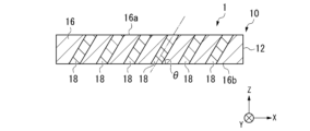
図1及び図2に示すように、実施形態の一例の異方導電性コネクタ1は、複数列の導電帯部12を含むシート状の導電部10を備えている。導電部10では、複数列の導電帯部12が平行に並んでおり、隣り合う互いの導電帯部12が接着部14を介して接着されている。ここで、複数列の導電帯部12が平行に延びている方向を長さ方向(図1及び図2のX方向)、複数列の導電帯部12の接着部14を介した積層方向を幅方向(図1及び図2のY方向)、長さ方向と幅方向の両方に垂直な方向を厚さ方向(図1及び図2のZ方向)とする。
[Anisotropic conductive connector]
As shown in Figures 1 and 2, an anisotropic
導電帯部12は、絶縁性を有する弾性材料からなる帯状の絶縁部16と、絶縁部16の厚さ方向(Z方向)の第1面16aから第2面16bまで貫通し、かつ絶縁部16の長さ方向(X方向)に一定のピッチで配列された複数の銀線18と、を備えている。なお、銀線には、銀合金からなる導電線も含まれる。The
絶縁部16の厚さは、用途に応じて適宜設定すればよく、例えば、0.07mm以上2.0mm以下とすることができる。絶縁部16の厚さは、測定顕微鏡などの拡大観察手段によって、絶縁部16の厚さ方向の断面から任意に選択した10箇所の厚さを測定した値の平均値として求められる。The thickness of the
帯状の絶縁部16の長さ及び幅は、特に限定されず、適宜設定することができる。絶縁部16の長さは、例えば、2mm以上50mm以下とすることができる。絶縁部16の幅は、例えば、0.03mm以上0.25mm以下とすることができる。絶縁部16の長さ及び幅は、いずれも任意に選択した10箇所で測定した値の平均値として求められる。The length and width of the strip-shaped
絶縁部16を構成する材料は、絶縁性を有する弾性材料であり、例えば、ウレタンゴム、イソプレンゴム、エチレンプロピレンゴム、天然ゴム、エチレンプロピレンジエンゴム、スチレンブタジエンゴム、シリコーンゴム等のエラストマーを例示できる。これらの中でも、圧縮永久歪が小さい点から、シリコーンゴムが好ましい。シリコーンゴムは、縮合型シリコーンゴムであってもよく、付加型シリコーンゴムであってもよい。絶縁部16を構成する弾性材料には、シランカップリング剤、接着助剤、抗酸化剤、染料、顔料、充填剤、レベリング剤等の添加剤が含まれていてもよい。The material constituting the insulating
絶縁部16の圧縮永久歪は、20%以下が好ましく、18%以下がより好ましい。絶縁部16の圧縮永久歪が前記上限値以下であれば、検査時の電気電子部品の圧接による圧縮や、温度、湿度等の環境条件の変化によって生じる膨張や収縮に容易に追従できるため、より安定した接続が確保できる。また、使用時の異方導電性コネクタ1の厚さ方向の圧縮量を広範囲に設定できる。絶縁部16の圧縮永久歪の下限は特に限定されず、小さければ小さいほどよい。
なお、絶縁部16の圧縮永久歪は、JIS K 6262(85℃×24hr、25%圧縮)に従って測定される。
The compression set of the
The compression set of the
導電帯部12では、複数の銀線18が帯状の絶縁部16の長さ方向(X方向)に一定のピッチで配列されている。銀線18のピッチ、すなわち絶縁部16の第1面16a側から見た銀線18の中心間距離は、特に制限されず、例えばインピーダンスのシミュレーション結果に応じて任意に設定することができる。例えば銀線18のピッチは5μm以上100μm以下とすることができる。銀線18のピッチは、任意に選択した10組の隣り合う銀線18の中心間距離を測定した値の平均値として求められる。In the
図2に示す例では、銀線18は、絶縁部16の第2面16bに対して傾斜して設けられている。
銀線18が絶縁部16の第2面16bに対して傾斜している構成の異方導電性コネクタ1は、銀線18が絶縁部16の第2面16bに垂直になっている構成に比べて、厚さ方向への繰り返しの圧縮に対する耐性に優れることから、電子デバイス部品、モジュール部品等の電気電子部品の検査用として特に有用である。
なお、異方導電性コネクタ1の用途は、電気電子部品の検査用には限定されず、例えば電子デバイス部品、モジュール部品等の基板間の電極同士を電気的に接続する等、いわゆる電気電子部品への実装用として用いてもよい。
In the example shown in FIG. 2 , the
The anisotropic
The use of the anisotropic
絶縁部16の第2面16bに対する銀線18の傾斜角度θは、50度以上が好ましく、55度以上がより好ましく、60度以上がさらに好ましい。銀線18の傾斜角度θが前記下限値以上であれば、圧縮時における銀線の座屈(塑性変形)を抑えやすい。銀線18の傾斜角度θは、75度以下が好ましく、70度以下がより好ましく、65度以下がさらに好ましい。銀線18の傾斜角度θが前記上限値以下であれば、圧縮時における初期コンタクト性が改善される。銀線18の傾斜角度θの好ましい下限と上限は任意に組み合わせることができ、例えば50~75度が好ましく、55~70度がより好ましく、60~65度がさらに好ましい。銀線18の傾斜角度θは、任意に選択した10本の銀線18の傾斜角度の平均値として求められる。
なお、絶縁部16の第2面16bに対する銀線18の傾斜角度θは、絶縁部16の第2面16bと、銀線18の中心軸とのなす角度における劣角(0<θ<90)を意味するものとする。
The inclination angle θ of the
The inclination angle θ of the
銀線18は、銅合金線、真鍮線等の従来の導電線に比べて柔軟である。導電線として柔軟な銀線18を用いることで、電気電子部品の検査時や、電気電子部品への実装時において、低抵抗かつ低荷重で銀線を電気電子部品の電極に接続することが可能となる。これにより、検査対象の電極が傷付きにくくなり、酸化異物の堆積が最小限に抑制されるため、抵抗値が経時的に上昇することを抑制することができる。また、異方導電性コネクタ1が圧縮された際に銀線18が座屈しにくく、絶縁部16の変形に追従しやすいため、電極と接触する銀線18の先端部が絶縁部16に潜り込みにくくなることから、電極間の電気的な接続が安定になる。さらに、銀線18を用いれば、コンパクトな電気電子部品に対しても、その電極形状やピッチに合わせて容易に銀線18を狭いピッチで配列することができ、1つの電極に複数の銀線18を接触させることができるため、接続安定性がさらに優れる。The
銀線18の引張強度は、200N/mm2以上が好ましく、220N/mm2以上がより好ましい。銀線18の引張強度が前記範囲の下限値以上であれば、周辺の絶縁部16の変形に追従しやすくなる。また、銀線18の引張強度は、380N/mm2以下が好ましく、360N/mm2以下がより好ましい。銀線18の引張強度が前記範囲の上限値以下であれば、座屈し難く絶縁部16に潜りにくくなり接続が安定する。銀線18の引張強度の下限と上限は任意に組み合わせることができ、例えば200N/mm2以上380N/mm2以下が好ましい。
なお、銀線18の引張強度は、例えばJIS Z 2241に準拠した引張試験機、具体的にはロードセルとしてUR-10N-Dを用いたテンシロン万能材料試験機RTI-1225(株式会社エー・アンド・デイ製)などを用い、試料長さ(上下チャック間の距離)を100mm、引張速度を20mm/minとして引張試験を行い、試料に加えた試験力の最大値を該試料の断面で除した値として求められる。
The tensile strength of the
The tensile strength of the
銀線18の破断点伸度は、0.90%以上が好ましく、1.00%以上がより好ましく、1.10%以上がさらに好ましい。また、銀線18の破断点伸度は、1.30%以下が好ましく、1.25%以下がより好ましく、1.20%以下がさらに好ましい。銀線18の破断点伸度が前記下限と上限で示される範囲内であれば、後述の製品切断工程時における銀線の変形を抑制しやすい。銀線18の破断点伸度の好ましい下限と上限は、任意に組み合わせることができ、例えば0.90~1.30%が好ましく、1.00~1.25%がより好ましく、1.10~1.20%がさらに好ましい。
前記破断点伸度は、JIS Z 2241に従って測定される値である。
The breaking point elongation of the
The elongation at break is a value measured in accordance with JIS Z 2241.
銀線18の最大点荷重は、0.14N以上が好ましく、0.15N以上がより好ましく、0.16N以上がさらに好ましい。また、銀線18の最大点荷重は、0.20N以下が好ましく、0.18N以下がより好ましく、0.17N以下がさらに好ましい。銀線18の最大点荷重が前記下限と上限で示される範囲内であれば、検査対象となる電気電子部品の電極の傷付きを抑制しやすい。銀線18の最大点荷重の好ましい下限と上限は、任意に組み合わせることができ、例えば0.14~0.20Nが好ましく、0.15~0.18Nがより好ましく、0.16~0.17Nがさらに好ましい。
前記最大点荷重は、JIS Z 2241に従って測定される値である。
The maximum point load of the
The maximum point load is a value measured in accordance with JIS Z 2241.
銀線18の0.2%耐力荷重は、0.12N以上が好ましく、0.13N以上がより好ましく、0.14N以上がさらに好ましい。また、銀線18の0.2%耐力荷重は、0.18N以下が好ましく、0.17N以下がより好ましく、0.16N以下がさらに好ましい。銀線18の0.2%耐力荷重の好ましい下限と上限は、任意に組み合わせることができ、例えば0.12~0.18Nが好ましく、0.13~0.17Nがより好ましく、0.14~0.16Nがさらに好ましい。
前記0.2%耐力荷重は、JIS Z 2241に従って測定される値である。
The 0.2% proof stress load of the
The 0.2% proof load is a value measured in accordance with JIS Z 2241.
銀線の最大点荷重及び0.2%耐力荷重は、銀線の線径に依存する。そのため、銀線の線径を調節することにより、銀線の最大点荷重及び0.2%耐力荷重を調節することができる。 The maximum point load and 0.2% yield load of the silver wire depend on the wire diameter. Therefore, by adjusting the wire diameter of the silver wire, the maximum point load and 0.2% yield load of the silver wire can be adjusted.
銀線18は側面に被覆層が形成されていてもよい。被覆層の材料としては、例えば、金、ニッケル、銅等を例示できる。被覆層は1層でもよく、2層以上でもよい。
真鍮線及びベリリウム銅線などの銅合金線と異なり単体での酸化膜形成が無く、素材としては安定している点、銀線18の周囲の絶縁部16との接着性に優れる点から、後述の実験例では金めっき1層の銀線を用いている。
A coating layer may be formed on the side surface of the
Unlike copper alloy wires such as brass wire and beryllium copper wire, silver wire does not form an oxide film on its own and is a stable material. In addition, the
銀線18の長さ方向に対して直交する方向の断面の形状は、特に制限されず、例えば、略円形、略楕円形、略四角形を例示できる。
銀線18の線径は、例えば、5μm以上50μm以下とすることができる。銀線18の線径は、銀線18の長さ方向に直交する断面を含む最小円の直径である。銀線18が側面に被覆層を有する場合、銀線18の線径には被覆層も含む。
異方導電性コネクタ1が備える複数の銀線18の断面形状及び線径は、互いに同じでもよく、異なっていてもよい。
The shape of the cross section of the
The wire diameter of the
The cross-sectional shapes and wire diameters of the
銀線18における絶縁部16の第1面16a側の端部は、絶縁部16の第1面16aから突出していてもよい。同様に、銀線18における絶縁部16の第2面16b側の端部は、絶縁部16の第2面16bから突出していてもよい。銀線18における絶縁部16の第1面16a又は第2面16bから突出している部分の長さは、例えば1μm以上60μm以下とすることができる。The end of the
接着部14を形成する接着剤としては、特に限定されず、例えば、公知の硬化型接着剤を例示できる。接着部14を形成する接着剤は、1種でもよく、2種以上でもよい。
接着部14の長さ及び厚さは、隣り合う導電帯部12同士を十分に接着できる範囲で設定すればよく、例えば絶縁部の長さ及び厚さと同じにすることができる。接着部14の幅は、特に限定されず、例えば、0.01mm以上0.05mm以下とすることができる。接着部14の厚さ、長さ及び幅は、いずれも任意に選択した10箇所で測定した値の平均値として求められる。
There are no particular limitations on the adhesive that forms the
The length and thickness of the
異方導電性コネクタ1の平面視の形状は、この例では矩形であるが、矩形に限定されず、円形、楕円形、矩形、多角形等であってもよい。異方導電性コネクタ1の寸法は、用途に応じて適宜設定すればよく、例えば縦5mm以上50mm以下、横5mm以上100mm以下の矩形とすることができる。The shape of the anisotropic
異方導電性コネクタ1を厚さ方向(Z方向)から見たときの銀線18の配置パターンは、特に限定されず、例えば、各々の帯状の絶縁部16の長さ方向(X方向)に並んで配置されている複数の銀線18が、それぞれ絶縁部16の幅方向(Y方向)においても直線的に並んでいる2次元アレイ状の配置を例示できる。この場合、絶縁部16の幅方向(Y方向)に並ぶ銀線18のピッチは、例えば帯状の絶縁部16の長さ方向(X方向)に並ぶ銀線18のピッチと同じにすることができる。また、銀線18の配置パターンは、千鳥状等であってもよい。The arrangement pattern of the
異方導電性コネクタ1を厚さ方向から見たときの導電部10における銀線18の配線密度は、用途に応じて適宜設定でき、例えば、10本/mm2以上1,100本/mm2以下とすることができる。銀線18の配線密度は、絶縁部16の長さ方向における銀線18のピッチ、絶縁部16の幅、接着部14の幅等を調節することによって調節できる。
The wiring density of the
[異方導電性コネクタの製造方法]
以下、異方導電性コネクタ1の製造方法について説明する。
異方導電性コネクタ1の製造方法は、特に限定されず、導電線として銀線を用いる以外は公知の方法を採用することができる。本実施態様の異方導電性コネクタ1の製造方法は、例えば、後述するコアシート形成工程と、積層工程と、切断工程と、を含む。
[Method of manufacturing anisotropic conductive connector]
A method for manufacturing the anisotropic
The manufacturing method of the anisotropic
(コアシート形成工程)
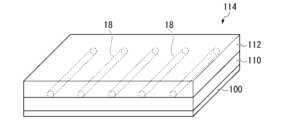
図3に示すように、絶縁部16を形成するための絶縁性を有する弾性材料によって第1絶縁層110を基材100の表面に形成し、第1絶縁層110の上面110aに複数の銀線18を一定の間隔をあけて平行に配置する。基材100は、その表面に第1絶縁層110を形成可能なものであれば特に制限されず、例えば樹脂シート、金属板、ガラス板等の平面を有する部材を例示できる。
(Core sheet forming process)
3, a first insulating
図4に示すように、絶縁部16を形成するための絶縁性を有する弾性材料によって、銀線18を覆うように第1絶縁層110の表面に第2絶縁層112を形成し、コアシート114を得る。As shown in FIG. 4, a second insulating
(積層工程)
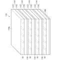
同様にして複数枚のコアシート114を作成し、不要な基材100を取り除いて、図5に示すように、接着層116を介して複数枚のコアシート114を積層したシート積層体118を得る。接着層116に用いる接着剤は、接着部14を形成する接着剤である。シート積層体118においては、各々のコアシート114が有する銀線18の長さ方向を揃える。
(Lamination process)
A plurality of
(切断工程)
各々の銀線18の長さ方向に対して傾斜する方向に、シート積層体118の上面118a側から刃を入れてシート積層体118を切断し、所望の厚さのシート状の異方導電性コネクタ1を得る。
(Cutting process)
The
以上説明したように、本発明の異方導電性コネクタにおいては、柔軟な銀線が、絶縁部の厚さ方向に対して傾斜して設けられている。そのため、例えば電気電子部品の検査時に繰り返し圧縮されたときや、実装した電気電子部品に温度、湿度等の環境条件の変化によって膨張や収縮が繰り返し起こったときでも、銀線と接触する電極に摩耗痕が生じにくく、酸化異物の堆積が低減されるため、経時的な抵抗値の上昇を抑制することができる。As described above, in the anisotropic conductive connector of the present invention, the flexible silver wire is provided at an angle to the thickness direction of the insulating part. Therefore, even when the electrical and electronic components are repeatedly compressed during inspection, or when the mounted electrical and electronic components repeatedly expand and contract due to changes in environmental conditions such as temperature and humidity, wear marks are unlikely to occur on the electrodes in contact with the silver wire, and the accumulation of oxidized foreign matter is reduced, making it possible to suppress an increase in resistance value over time.
また、銀線を用いた本発明の異方導電性コネクタは、接続対象の電極のコプラナリティ(共平面性)に応じて厚みを変化させることが容易である。
また、銀線を用いれば、高周波用途などインピーダンスのシミュレーション結果に応じ、狭いピッチで配列することができる。さらに、高周波特性用途の電子デバイス、モジュール部品の場合には、異方導電性コネクタの厚みを薄くすることで導通経路がはんだ実装並みの薄さとなるため、実装時と同等の特性で検査を行うことができる。
Furthermore, the anisotropic conductive connector of the present invention using silver wires can easily have its thickness changed in accordance with the coplanarity of the electrodes to be connected.
In addition, if silver wires are used, they can be arranged at a narrow pitch according to the results of impedance simulations for high frequency applications, etc. Furthermore, in the case of electronic devices and module components for high frequency applications, the thickness of the anisotropic conductive connector can be reduced to make the conductive path as thin as that of solder mounting, so that inspection can be performed with the same characteristics as when mounted.
なお、本発明の異方導電性コネクタは、前記した異方導電性コネクタ1には限定されない。
例えば、複数の銀線がそれぞれ絶縁部の第2面に対して傾斜して設けられる構成には限定されず、複数の銀線がそれぞれ絶縁部の第2面に対して垂直に設けられていてもよい。
銀線が絶縁部の第2面に対して垂直である場合、傾斜して設けられるよりも繰り返し圧縮特性(耐久性)は劣るが、薄膜により導通経路が最短で形成できることから、導通経路の長いプローブピンに比べて格段に高周波特性の減衰が抑制できる傾向がある。またLGA(Land Grid Array)などの高周波デバイス、モジュール部品などの実装用途では、ACF(異方性導電フィルム)、はんだ実装と比較するとデバイス等の不具合時による交換が容易になる。
The anisotropic conductive connector of the present invention is not limited to the anisotropic
For example, the configuration is not limited to one in which the multiple silver wires are each provided at an angle to the second surface of the insulating portion, and the multiple silver wires may each be provided perpendicular to the second surface of the insulating portion.
When the silver wire is perpendicular to the second surface of the insulating part, the repeated compression characteristics (durability) are inferior to when it is inclined, but since the conductive path can be formed in the shortest possible time by the thin film, the attenuation of high frequency characteristics tends to be significantly suppressed compared to a probe pin with a long conductive path. Also, in mounting applications such as high frequency devices and module parts such as LGA (Land Grid Array), replacement due to device malfunction is easier than ACF (Anisotropic Conductive Film) and solder mounting.
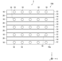
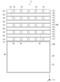
また、本発明の異方導電性コネクタは、銀線が設けられていない絶縁部をさらに含む導電部を備えるものであってもよい。具体的には、例えば図6に例示した異方導電性コネクタ2であってもよい。図6における図1と同じ部分は同符号を付して説明を省略する。The anisotropic conductive connector of the present invention may also have a conductive portion that further includes an insulating portion in which no silver wire is provided. Specifically, it may be, for example, the anisotropic
異方導電性コネクタ2は、帯状の絶縁部16に複数の銀線18が設けられた導電帯部12と、銀線18が設けられていない帯状の絶縁部20とが幅方向(Y方向)に交互に平行して並んで配置され、それらが接着部14を介して接着された導電部10Aを備えている。このように、導電部は、絶縁部に複数の銀線が設けられた導電帯部と、銀線が設けられていない絶縁部とを含むものであってもよい。The anisotropic
絶縁部20の厚さ及び長さは、用途に応じて適宜設定すればよく、例えば絶縁部16の厚さ及び長さと同じにすることができる。絶縁部20の幅は、銀線18の配線密度等に応じて適宜設定すればよく、例えば、0.1mm以上0.5mm以下とすることができる。絶縁部20を構成する材料は、絶縁部16を構成する材料と同じ絶縁性を有する弾性材料を例示でき、好ましい態様も同じである。
絶縁部20の圧縮永久歪は、絶縁部16の圧縮永久歪と同じ理由から、20%以下が好ましく、18%以下がより好ましい。
The thickness and length of the insulating
For the same reasons as those for the compression set of the insulating
本発明の異方導電性コネクタは、例えば図7に例示した異方導電性コネクタ3であってもよい。図7における図1及び図6と同じ部分は同符号を付して説明を省略する。
異方導電性コネクタ3は、導電部10Aに加えて、導電部10Aにおける絶縁部16の幅方向(Y方向)の隣りに接着部14を介して接着された貼付け部22をさらに備えている以外は、異方導電性コネクタ2と同様の構成である。
The anisotropic conductive connector of the present invention may be, for example, the anisotropic
The anisotropic
貼付け部22は、平面視矩形状の絶縁部24と、絶縁部24の厚さ方向の第1面24a側に設けられた接着層26と、を備えている。
異方導電性コネクタ3は、貼付け部22を備えていることで、検査装置における回路基板の電極端子が設けられた側や、電子デバイス部品、モジュール部品等の電気電子部品における回路基板の電極が設けられた側に、接着層26を介して直に貼り付けることができる。また、回路基板に異方導電性コネクタ3を貼り付けてそれらを一体に扱うことができるため、電気電子部品や検査装置を、機械を用いた自動製造にも容易に適用できる。
The
The anisotropic
近年は電子機器の省スペース化に伴って電子デバイス部品やモジュール部品がコンパクト化されており、また実装強度を高める目的でダミー電極(ホールドダウン)が用いられることから電極の数も多いため、電極同士の位置決めが難しい。さらに、多電極を要する電気電子部品、検査装置等では、不良があるとリペア作業が非常に大変である。しかし、接着層26を介して貼り付ける異方導電性コネクタ3であれば、はんだ実装に比べて位置決めが容易であり、またリペア作業での交換も容易である。In recent years, electronic device components and module components have become more compact in line with the trend to reduce the space required for electronic devices. In addition, dummy electrodes (hold downs) are used to increase mounting strength, resulting in a large number of electrodes, making it difficult to position the electrodes relative to one another. Furthermore, in electrical and electronic components and inspection devices that require multiple electrodes, repair work is extremely difficult if there is a defect. However, with the anisotropic
絶縁部24の形状及び寸法は、適宜設定すればよく、例えば、縦2mm以上50mm以下、横5mm以上100mm以下の矩形とすることができる。
絶縁部24を構成する材料は、絶縁部16を構成する材料と同じ絶縁性を有する弾性材料を例示でき、好ましい態様も同じである。
The shape and dimensions of the insulating
The material constituting the insulating
接着層26を形成する接着剤としては、特に限定されず、例えば、公知の硬化型接着剤を例示できる。接着層26を形成する接着剤は、1種でもよく、2種以上でもよい。
接着層26の厚さは、異方導電性コネクタ3を安定して基板に貼る付けることができる範囲で設定すればよく、例えば0.01mm以上0.04mm以下とすることができる。接着層26の厚さは、任意に選択した10箇所で測定した値の平均値として求められる。
There are no particular limitations on the adhesive that forms the
The thickness of the
[フレーム付き異方導電性コネクタ]
本発明の異方導電性コネクタには、その周囲に位置決めのためのフレームが結合されていてもよい。
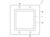
フレーム付き異方導電性コネクタの一例の概略構成を図8に示す。
フレーム付き異方導電性コネクタ4は、異方導電性コネクタ1の周囲に、全周にわたって環状のフレーム30が結合されている。
[Anisotropic conductive connector with frame]
The anisotropic conductive connector of the present invention may have a frame bonded to its periphery for positioning.
FIG. 8 shows a schematic configuration of one example of a framed anisotropic conductive connector.
The framed anisotropically conductive connector 4 has an
フレーム30は、中央の領域が矩形に打ち抜かれており、この領域に接着材32を介して異方導電性コネクタ1が結合されている。異方導電性コネクタ1の上面とフレーム30の上面とは互いにほぼ平行な面となっている。
フレーム30には、複数の貫通孔34が設けられている。フレーム付き異方導電性コネクタ4を基板等に実装する際には、例えばフレーム30の貫通孔34に位置決めピンを通して固定することにより、基板等への実装を容易に行うことができる。
The
The
フレーム30の平面視形状は、図8に示す例では矩形であるが、限定されるものではない。フレーム30は、異方導電性コネクタ1の全周を囲う環状には限定されず、異方導電性コネクタ1の周囲の1箇所又は複数箇所に部分的に結合されているものであってもよい。
フレーム30のサイズは、異方導電性コネクタ1を実装する対象に応じて適宜設計すればよい。
フレーム30の材質は特に限定されず、例えば樹脂製のフレーム、金属製のフレーム等とすることができる。
8, the shape of the
The size of the
The material of the
接着材32は接着剤の硬化物であり、異方導電性コネクタ1の使用温度域において硬化状態を安定に保つ耐熱性、耐寒性を有するものが選択される。具体的には、例えば、アクリル樹脂、シリコーン、アクリル変性シリコーン、シアノアクリレート樹脂を例示できる。
フレーム30における接着材32の接着面には、予めプライマー処理を施し、接着力を高めてもよい。
The adhesive 32 is a cured product of an adhesive, and is selected from those having heat resistance and cold resistance that allow the cured state to be kept stable in the operating temperature range of the anisotropic
The adhesive surface of the
フレーム付き異方導電性コネクタの製造方法は、特に限定されず、本発明の異方導電性コネクタを用いる以外は公知の方法を利用することができる。
なお、本発明のフレーム付き異方導電性コネクタは、本発明の異方導電性コネクタを備えるものであれば、前記したフレーム付き異方導電性コネクタ4には限定されず、適用する検査装置や電気電子部品等に応じて適宜設計を変更できる。
The method for producing the framed anisotropically conductive connector is not particularly limited, and any known method can be used as long as the anisotropically conductive connector of the present invention is used.
In addition, the frame-equipped anisotropic conductive connector of the present invention is not limited to the frame-equipped anisotropic conductive connector 4 described above, so long as it is equipped with the anisotropic conductive connector of the present invention, and the design can be appropriately changed depending on the inspection device, electrical and electronic components, etc. to be applied.
[検査装置]
本発明の異方導電性コネクタは、電子デバイス部品、モジュール部品等の電気電子部品を検査するための検査装置に用いることができる。
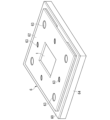
図9は、本発明の異方導電性コネクタを備える検査装置の一例を示した斜視図である。
[Inspection equipment]
The anisotropic conductive connector of the present invention can be used in an inspection apparatus for inspecting electric and electronic components such as electronic device components and module components.
FIG. 9 is a perspective view showing an example of an inspection device equipped with the anisotropic conductive connector of the present invention.
図9に示す例の検査装置5は、電極端子を備える回路基板50と、異方導電性コネクタ1と、ホルダ52と、プレート54と、を備えている。The
回路基板50としては、電極端子を備える回路基板であればよく、例えばプリント配線基板を用いることができる。この例では、回路基板50はプレート54上に配置されているが、この態様には限定されない。
プレート54の材質は特に限定されず、樹脂製であってもよく、金属製であってもよい。
The
The material of the
ホルダ52は、異方導電性コネクタ1の外周部分を回路基板50上に固定するための部材である。この例のホルダ52は、矩形の枠における一辺に、一部が欠けた欠け部分52aを有するC字状になっている。なお、ホルダ52の形状は、この例の形状は限定されず、例えば欠け部分のない枠状であってもよい。
ホルダ52の材質は特に限定されず、樹脂製であってもよく、金属製であってもよい。
The
The material of the
検査装置5では、回路基板50上に異方導電性コネクタ1が配置され、さらにその上にホルダ52が配置された状態で、ボルト53がホルダ52のボルト孔に螺挿されている。これにより、異方導電性コネクタ1の外周部分が回路基板50とホルダ52で挟持されることで、異方導電性コネクタ1が回路基板50上に固定されている。この状態では、回路基板50に設けられた電極端子が異方導電性コネクタ1における銀線18の回路基板50側の端部と接している。In the
例えば検査対象の回路基板としてフレキシブルプリント配線基板210を備える電気電子部品200を検査する場合、異方導電性コネクタ1の回路基板50側とは反対側における、ホルダ52が接していないT字状の領域にフレキシブルプリント配線基板210を嵌め込んで圧接する。そして、電気電子部品200のフレキシブルプリント配線基板210に設けられた電極を、検査装置5の異方導電性コネクタ1における銀線18の回路基板50側とは反対側の端部に接触させる。
これにより、検査装置5における回路基板50の電極端子と、検査対象のフレキシブルプリント配線基板210の電極とが、異方導電性コネクタ1の銀線18を介して電気的に接続され、検査を行うことができる。
For example, when inspecting an electric/
As a result, the electrode terminals of the
検査装置5の製造方法は、特に限定されず、本発明の異方導電性コネクタを用いる以外は公知の方法を利用することができる。The manufacturing method of the
なお、本発明の検査装置は、本発明の異方導電性コネクタを備えるものであれば、前記した検査装置5には限定されず、適用する電子デバイス部品、モジュール部品等に応じて適宜設計を変更できる。
In addition, the inspection device of the present invention is not limited to the above-mentioned
例えば、図10に例示した検査装置(ソケット)6であってもよい。検査装置6は、電極端子を備える回路基板60と、異方導電性コネクタ1と、ホルダ62と、プレート64と、を備えている。For example, the inspection device (socket) 6 illustrated in Fig. 10 may be used. The
回路基板60としては、電極端子を備える回路基板であればよく、例えばプリント配線基板を用いることができる。この例では、回路基板60はプレート64上に配置されているが、この態様には限定されない。
プレート64の材質は特に限定されず、樹脂製であってもよく、金属製であってもよい。
The
The material of the
ホルダ62は、異方導電性コネクタ1の外周部分を回路基板50上に固定するための部材であり、矩形の枠状である。
ホルダ62の材質は特に限定されず、樹脂製であってもよく、金属製であってもよい。
The
The material of the
検査装置6では、回路基板60上に異方導電性コネクタ1が配置され、さらにその上にホルダ62が配置された状態で、ボルト63がホルダ62のボルト孔に螺挿されている。これにより、異方導電性コネクタ1の外周部分が全周にわたって回路基板60とホルダ62で挟持されることで、異方導電性コネクタ1が回路基板60上に固定されている。この状態では、回路基板60に設けられた電極端子が異方導電性コネクタ1における銀線18の回路基板60側の端部と接している。In the
検査時には、例えばBGA、QFN、SOP、QFP、CSP等の半導体デバイスをホルダ62の内側に嵌め込み、異方導電性コネクタ1の回路基板60側とは反対側に圧接する。そして、半導体デバイスの電極を、検査装置6の異方導電性コネクタ1における銀線18の回路基板60側とは反対側の端部に接触させる。
これにより、検査装置6における回路基板60の電極端子と、半導体デバイスの電極とが、異方導電性コネクタ1の銀線18を介して電気的に接続され、検査を行うことができる。
During inspection, a semiconductor device such as BGA, QFN, SOP, QFP, CSP, etc. is fitted inside the
As a result, the electrode terminals of the
検査装置6の製造方法は、特に限定されず、本発明の異方導電性コネクタを用いる以外は公知の方法を利用することができる。The manufacturing method of the
本発明の検査装置は、フレーム付き異方導電性コネクタを備えるものであってもよい。より具体的には、位置決めピンやホルダ等によってフレーム付き異方導電性コネクタが回路基板に固定され、そのフレーム付き異方導電性コネクタの回路基板側とは反対側に、検査対象の電気電子部品の回路基板が圧接される検査装置であってもよい。The inspection device of the present invention may be equipped with a framed anisotropic conductive connector. More specifically, the inspection device may be one in which a framed anisotropic conductive connector is fixed to a circuit board by a positioning pin, a holder, or the like, and a circuit board of an electric/electronic component to be inspected is pressed against the side of the framed anisotropic conductive connector opposite the circuit board.
以下、実施例によって本発明を詳細に説明するが、本発明は以下の記載によっては限定されない。The present invention will now be described in detail with reference to examples, but the present invention is not limited to the following description.
[初期コンタクト性の評価試験]
下記の試験設備を用い、金めっき付きベタ電極上に異方導電性コネクタを置き、ロードセル先端に取り付けた金めっき付きピン電極によって異方導電性コネクタを圧縮した際の荷重値と抵抗値を測定した。
(試験設備)
試験機:自動荷重試験機(MAX-1KN-M、日本計測システム株式会社製)
ロードセル:JLC-M50N(50N)
測定電極:Φ0.14mmの金めっき付きピン電極、金めっき付きベタ電極
抵抗計:RM3545-02(日置電機製)
測定条件:圧縮量制御(異方導電性コネクタの厚さに対して50%)
試験速度:1mm/min
[Evaluation test of initial contact properties]
Using the test equipment described below, the anisotropic conductive connector was placed on a gold-plated solid electrode, and the load and resistance values were measured when the anisotropic conductive connector was compressed by a gold-plated pin electrode attached to the tip of a load cell.
(Testing equipment)
Testing machine: Automatic load testing machine (MAX-1KN-M, manufactured by Japan Measurement Systems Co., Ltd.)
Load cell: JLC-M50N (50N)
Measurement electrodes: Φ0.14 mm gold-plated pin electrodes, gold-plated solid electrodes Resistance meter: RM3545-02 (manufactured by Hioki E.E.)
Measurement conditions: compression amount control (50% relative to the thickness of the anisotropic conductive connector)
Test speed: 1 mm/min
[実験例1]
ポリエステルフィルム(基材)の上に未硬化のシリコーンゴム(信越化学工業社製)からなる厚さ約0.025mmの塗膜(第1絶縁層)を形成し、この塗膜上に導電線として金めっき付きベリリウム銅線(線径23μm、破断点伸度:1.29%、最大点荷重:0.58N、0.2%耐力荷重:0.35N)を0.05mm程度の間隔でそれぞれ平行に配置した。シリコーンゴムによって、これら導電線を覆う厚さ約0.025mmの塗膜(第2絶縁層)を形成し、加熱硬化してコアシートを得た。同様に複数枚のコアシートを作成して、それらを接着剤により、互いの導電線の長さ方向が平行に揃うように積層してシート積層体を得た。
前記シート積層体をスライスカットすることにより、絶縁部の長さ方向(X方向)と幅方向(Y方向)の導電線のピッチがいずれも0.05mmであり、導電線の傾斜角度θが63.4度であり、厚さが0.15mmである異方導電性コネクタを得た。
得られた異方導電性コネクタについて初期コンタクト性の評価試験を行った。その結果を図11に示す。
[Experimental Example 1]
A coating film (first insulating layer) of about 0.025 mm thick made of uncured silicone rubber (manufactured by Shin-Etsu Chemical Co., Ltd.) was formed on a polyester film (substrate), and gold-plated beryllium copper wires (wire diameter 23 μm, elongation at break: 1.29%, maximum point load: 0.58 N, 0.2% yield load: 0.35 N) were arranged on the coating film as conductive wires at intervals of about 0.05 mm in parallel. A coating film (second insulating layer) of about 0.025 mm thick covering these conductive wires was formed using silicone rubber, and the core sheet was obtained by heating and curing. Similarly, multiple core sheets were prepared and laminated with an adhesive so that the length directions of the conductive wires were aligned parallel to each other to obtain a sheet laminate.
The sheet laminate was sliced to obtain an anisotropic conductive connector having a pitch of the conductive wires in both the length direction (X direction) and width direction (Y direction) of the insulating part of 0.05 mm, an inclination angle θ of the conductive wires of 63.4 degrees, and a thickness of 0.15 mm.
The anisotropic conductive connector thus obtained was subjected to an evaluation test for initial contact property, and the results are shown in FIG.
[実験例2]
導電線として、金めっき付き銀線(線径25μm、破断点伸度:1.17%、最大点荷重:0.17N、0.2%耐力荷重:0.15N)を用いた以外は、実験例1と同様にして異方導電性コネクタを製造し、初期コンタクト性の評価試験を行った。その結果を図12に示す。
[Experimental Example 2]
An anisotropic conductive connector was manufactured in the same manner as in Experimental Example 1, except that a gold-plated silver wire (wire diameter 25 μm, elongation at break: 1.17%, maximum point load: 0.17 N, 0.2% yield load: 0.15 N) was used as the conductive wire, and an evaluation test of the initial contact property was performed. The results are shown in FIG.
図11及び図12に示すように、銀線を用いた実験例2の異方導電性コネクタは、真鍮線を用いた実験例1の異方導電性コネクタに比べ、0.005mm程度の小さい圧縮量でも抵抗値が小さくなった。このように、銀線を用いた実験例2の異方導電性コネクタは、低抵抗かつ低荷重で銀線を電極と接続させることができた。11 and 12, the anisotropic conductive connector of Experimental Example 2 using silver wire had a smaller resistance value even with a small compression amount of about 0.005 mm compared to the anisotropic conductive connector of Experimental Example 1 using brass wire. Thus, the anisotropic conductive connector of Experimental Example 2 using silver wire was able to connect the silver wire to the electrode with low resistance and low load.
[繰り返し圧縮特性(耐久性)の評価試験]
下記の試験設備を用い、バックアッププレートからなる評価治具を荷重試験機に設置し、さらにその上に評価基板、異方導電性コネクタ、及びPKGガイド(ただし、「PKG」はパッケージを意味する。)を順次設置した。先端に市販のダミーPKGを取り付けた金めっき付きピン電極をロードセル先端に設置し、1回毎の荷重値が20NとなるようにダミーPKGを異方導電性コネクタに繰り返し圧接し、抵抗値を測定した。
(試験設備)
試験機:自動荷重試験機(MAX-1KN-M、日本計測システム株式会社製)
ロードセル:JLC-M50N(50N)
ダミーPKG:WLP64T.3C-DC088D(ピッチ:0.3mm、はんだボール:Φ0.2mm)
測定電極:Φ1mm金めっき付きピン電極、WLP64用評価基板(デイジーチェーン接続)
抵抗計:RM3545-02(日置電機製)
測定条件:荷重制御(20N)
試験速度:6mm/min
測定間隔:25回毎(測定時1sec停止)
ダミーPKGの交換頻度:5,000回毎(繰り返し圧縮特性のみ)
[Evaluation test of repeated compression characteristics (durability)]
Using the following test equipment, an evaluation jig consisting of a backup plate was placed on a load tester, and an evaluation board, an anisotropic conductive connector, and a PKG guide (where "PKG" means package) were placed on top of the evaluation jig in that order. A gold-plated pin electrode with a commercially available dummy PKG attached to its tip was placed on the tip of a load cell, and the dummy PKG was repeatedly pressed against the anisotropic conductive connector so that the load value for each press was 20 N, and the resistance was measured.
(Testing equipment)
Testing machine: Automatic load testing machine (MAX-1KN-M, manufactured by Japan Measurement Systems Co., Ltd.)
Load cell: JLC-M50N (50N)
Dummy PKG: WLP64T.3C-DC088D (pitch: 0.3 mm, solder ball: Φ0.2 mm)
Measurement electrode: Φ1mm gold-plated pin electrode, WLP64 evaluation board (daisy chain connection)
Resistance meter: RM3545-02 (manufactured by Hioki E.E.)
Measurement conditions: Load control (20N)
Test speed: 6 mm/min
Measurement interval: Every 25 times (1 sec stop during measurement)
Dummy PKG replacement frequency: Every 5,000 times (repeated compression characteristics only)
[実験例3]
導電線として、金めっき付きベリリウム銅線(線径23μm、破断点伸度:1.29%、最大点荷重:0.58N、0.2%耐力荷重:0.35N)を用いた以外は、実験例1と同様にして異方導電性コネクタを製造し、繰り返し圧縮特性(耐久性)の評価試験を行った。その結果を図13に示す。
[Experimental Example 3]
An anisotropic conductive connector was manufactured in the same manner as in Experimental Example 1, except that a gold-plated beryllium copper wire (wire diameter 23 μm, elongation at break: 1.29%, maximum point load: 0.58 N, 0.2% yield load: 0.35 N) was used as the conductive wire, and an evaluation test of the repeated compression characteristics (durability) was performed. The results are shown in FIG.
[実験例4]
導電線として、金めっき付き銀線(線径25μm、破断点伸度:1.17%、最大点荷重:0.17N、0.2%耐力荷重:0.15N)を用いた以外は、実験例1と同様にして異方導電性コネクタを製造し、繰り返し圧縮特性(耐久性)の評価試験を行った。その結果を図14に示す。
なお、図13及び図14は、圧縮5000回毎のダミーPKG交換直後の1回目圧縮時のデータを纏めたものである。
[Experimental Example 4]
An anisotropic conductive connector was manufactured in the same manner as in Experimental Example 1, except that a gold-plated silver wire (wire diameter 25 μm, elongation at break: 1.17%, maximum point load: 0.17 N, 0.2% yield load: 0.15 N) was used as the conductive wire, and an evaluation test of the repeated compression characteristics (durability) was performed. The results are shown in FIG.
13 and 14 show a summary of data from the first compression immediately after replacing the dummy PKG every 5000 compressions.
図13及び図14に示すように、銀線を用いた実験例4の異方導電性コネクタは、圧縮回数が45,000回程度まで抵抗値がほとんど上昇せず、ベリリウム銅線を用いた実験例3の異方導電性コネクタに比べて連続的な使用における抵抗値の上昇を充分に抑制できることが分かった。 As shown in Figures 13 and 14, the anisotropic conductive connector of Experimental Example 4 using silver wire showed almost no increase in resistance up to approximately 45,000 compressions, and it was found that the increase in resistance during continuous use could be sufficiently suppressed compared to the anisotropic conductive connector of Experimental Example 3 using beryllium copper wire.
[実験例5]
導電線として、金めっき付き銀線(線径25μm、破断点伸度:1.17%、最大点荷重:0.17N、0.2%耐力荷重:0.15N、銀線の上に直接金めっき層を形成したもの)を用い、傾斜角度を90度、すなわち第2面に対して銀線を垂直に配した以外は、実験例1と同様にして異方導電性コネクタを製造し、初期コンタクト性の評価試験を行った。
その結果、初期コンタクト性及び繰り返し圧縮特性(耐久性)に関しては、導電線の座屈が生じるため図12及び図14の評価試験結果よりも若干劣る。
[Experimental Example 5]
An anisotropic conductive connector was manufactured in the same manner as in Experimental Example 1, except that a gold-plated silver wire (wire diameter 25 μm, elongation at break: 1.17%, maximum point load: 0.17 N, 0.2% yield load: 0.15 N, gold-plated layer formed directly on the silver wire) was used as the conductive wire and the inclination angle was 90 degrees, i.e., the silver wire was arranged perpendicular to the second surface, and an evaluation test of initial contact property was performed.
As a result, the initial contact property and repeated compression characteristics (durability) are slightly inferior to the evaluation test results shown in FIGS. 12 and 14 because buckling of the conductive wire occurs.
1~3…異方導電性コネクタ
4…フレーム付き異方導電性コネクタ
5,6…検査装置
10,10A…導電部
12…導電帯部
14…接着部
16…絶縁部
18…銀線
20…絶縁部
22…貼付け部
24…絶縁部
26…接着層
30…フレーム
32…接着材
34…貫通孔
50,60…回路基板
52,62…ホルダ
54,64…プレート
Claims (9)
JIS Z 2241に従って測定される前記銀線の引張強度が200N/mm 2 以上380N/mm 2 以下であり、
前記複数の銀線は、それぞれ前記絶縁部の前記第2面に対して垂直又は傾斜して設けられている、異方導電性コネクタ。 The insulating member includes a strip-shaped insulating portion made of an elastic material having insulating properties, and a plurality of silver wires that penetrate the insulating portion from a first surface to a second surface in a thickness direction and are arranged at a constant pitch in a longitudinal direction of the insulating portion,
The tensile strength of the silver wire measured in accordance with JIS Z 2241 is 200 N/mm2 or more and 380 N/mm2 or less,
An anisotropic conductive connector, wherein the plurality of silver wires are each arranged perpendicular or inclined to the second surface of the insulating portion.
請求項1に記載の異方導電性コネクタ。2. The anisotropic conductive connector according to claim 1.
請求項1に記載の異方導電性コネクタ。2. The anisotropic conductive connector according to claim 1.
請求項1に記載の異方導電性コネクタ。2. The anisotropic conductive connector according to claim 1.
前記異方導電性コネクタの外周部分の少なくとも一部が前記ホルダによって前記回路基板上に固定され、
前記電極端子が前記異方導電性コネクタにおける前記銀線の前記回路基板側の端部と接しており、
検査時には、前記異方導電性コネクタの前記回路基板と反対側の面における前記ホルダが接していない領域に前記電気電子部品を圧接し、前記電気電子部品が有する電極を前記異方導電性コネクタにおける前記銀線の前記回路基板側とは反対側の端部に接触させる、検査装置。 An inspection device for electric and electronic components, comprising: a circuit board having electrode terminals; the anisotropic conductive connector according to any one of claims 1 to 6 ; and a holder,
At least a part of an outer periphery of the anisotropic conductive connector is fixed onto the circuit board by the holder;
the electrode terminal is in contact with an end of the silver wire in the anisotropic conductive connector on the circuit board side,
During inspection, the electrical/electronic component is pressed against an area of the anisotropic conductive connector opposite the circuit board that is not in contact with the holder, and an electrode of the electrical/electronic component is brought into contact with an end of the silver wire in the anisotropic conductive connector opposite the circuit board.
前記フレーム付き異方導電性コネクタのフレーム部分の少なくとも一部が前記ホルダによって前記回路基板上に固定され、
前記電極端子が前記フレーム付き異方導電性コネクタにおける前記銀線の前記回路基板側の端部と接しており、
検査時には、前記フレーム付き異方導電性コネクタの前記回路基板と反対側の面における前記ホルダが接していない領域に前記電気電子部品を圧接し、前記電気電子部品が有する電極を前記フレーム付き異方導電性コネクタにおける前記銀線の前記回路基板側とは反対側の端部に接触させる、検査装置。 An inspection device for electric and electronic components, comprising: a circuit board having electrode terminals; the framed anisotropic conductive connector according to claim 7 ; and a holder,
At least a part of a frame portion of the framed anisotropic conductive connector is fixed onto the circuit board by the holder;
the electrode terminal is in contact with an end of the silver wire in the frame-attached anisotropic conductive connector on the circuit board side,
During inspection, the electrical/electronic component is pressed against an area of the framed anisotropic conductive connector on the side opposite the circuit board that is not in contact with the holder, and an electrode of the electrical/electronic component is brought into contact with an end of the silver wire in the framed anisotropic conductive connector on the side opposite the circuit board.
Applications Claiming Priority (1)
| Application Number | Priority Date | Filing Date | Title |
|---|---|---|---|
| PCT/JP2022/028084 WO2024018535A1 (en) | 2022-07-19 | 2022-07-19 | Anisotropically conductive connector, anisotropically conductive connector having frame, and inspection apparatus |
Publications (2)
| Publication Number | Publication Date |
|---|---|
| JPWO2024018535A1 JPWO2024018535A1 (en) | 2024-01-25 |
| JP7646090B2 true JP7646090B2 (en) | 2025-03-14 |
Family
ID=89617433
Family Applications (1)
| Application Number | Title | Priority Date | Filing Date |
|---|---|---|---|
| JP2024534813A Active JP7646090B2 (en) | 2022-07-19 | 2022-07-19 | Anisotropic conductive connector, framed anisotropic conductive connector and inspection device |
Country Status (6)
| Country | Link |
|---|---|
| US (1) | US20250208165A1 (en) |
| EP (1) | EP4560839A4 (en) |
| JP (1) | JP7646090B2 (en) |
| KR (1) | KR102981613B1 (en) |
| CN (1) | CN118575369A (en) |
| WO (1) | WO2024018535A1 (en) |
Citations (2)
| Publication number | Priority date | Publication date | Assignee | Title |
|---|---|---|---|---|
| WO2018190330A1 (en) | 2017-04-11 | 2018-10-18 | 信越ポリマー株式会社 | Electrical connector and method for manufacturing same |
| JP2021005522A (en) | 2019-06-27 | 2021-01-14 | 信越ポリマー株式会社 | Anisotropic conductive sheet with frame, manufacturing method thereof, and usage thereof |
Family Cites Families (10)
| Publication number | Priority date | Publication date | Assignee | Title |
|---|---|---|---|---|
| JPS61184283U (en) | 1985-05-09 | 1986-11-17 | ||
| US5049084A (en) * | 1989-12-05 | 1991-09-17 | Rogers Corporation | Electrical circuit board interconnect |
| JP2986364B2 (en) * | 1995-04-04 | 1999-12-06 | 信越ポリマー株式会社 | Method of manufacturing electrical connector |
| JP3020432B2 (en) * | 1995-06-14 | 2000-03-15 | 信越ポリマー株式会社 | Electrical connector and manufacturing method thereof |
| JPH1079281A (en) * | 1996-07-11 | 1998-03-24 | Sony Corp | Socket structure for semiconductor device test |
| JP3705366B1 (en) * | 2004-04-02 | 2005-10-12 | Jsr株式会社 | Circuit board inspection equipment |
| JP5615765B2 (en) * | 2011-06-24 | 2014-10-29 | 信越ポリマー株式会社 | Anisotropic conductive connector and method for manufacturing anisotropic conductive connector |
| JP2019125421A (en) | 2018-01-12 | 2019-07-25 | 株式会社協成 | Ic socket and floating pedestal thereof |
| CN115516712A (en) * | 2020-05-29 | 2022-12-23 | 三井化学株式会社 | Anisotropic conductive sheet, method for manufacturing anisotropic conductive sheet, electrical inspection device, and electrical inspection method |
| JP7342270B2 (en) * | 2020-07-10 | 2023-09-11 | 三井化学株式会社 | Anisotropically conductive sheet, method for manufacturing anisotropically conductive sheet, electrical testing device, and electrical testing method |
-
2022
- 2022-07-19 WO PCT/JP2022/028084 patent/WO2024018535A1/en not_active Ceased
- 2022-07-19 EP EP22951924.4A patent/EP4560839A4/en active Pending
- 2022-07-19 KR KR1020247025434A patent/KR102981613B1/en active Active
- 2022-07-19 US US18/729,505 patent/US20250208165A1/en active Pending
- 2022-07-19 JP JP2024534813A patent/JP7646090B2/en active Active
- 2022-07-19 CN CN202280090704.5A patent/CN118575369A/en active Pending
Patent Citations (2)
| Publication number | Priority date | Publication date | Assignee | Title |
|---|---|---|---|---|
| WO2018190330A1 (en) | 2017-04-11 | 2018-10-18 | 信越ポリマー株式会社 | Electrical connector and method for manufacturing same |
| JP2021005522A (en) | 2019-06-27 | 2021-01-14 | 信越ポリマー株式会社 | Anisotropic conductive sheet with frame, manufacturing method thereof, and usage thereof |
Also Published As
| Publication number | Publication date |
|---|---|
| WO2024018535A1 (en) | 2024-01-25 |
| KR20240129008A (en) | 2024-08-27 |
| JPWO2024018535A1 (en) | 2024-01-25 |
| KR102981613B1 (en) | 2026-06-23 |
| EP4560839A4 (en) | 2026-05-06 |
| US20250208165A1 (en) | 2025-06-26 |
| CN118575369A (en) | 2024-08-30 |
| EP4560839A1 (en) | 2025-05-28 |
Similar Documents
| Publication | Publication Date | Title |
|---|---|---|
| US5471151A (en) | Electrical interconnect using particle enhanced joining of metal surfaces | |
| US5506514A (en) | Electrical interconnect using particle enhanced joining of metal surfaces | |
| JP4987880B2 (en) | Circuit board connection structure using anisotropic conductive film, adhesion method, and adhesion state evaluation method using the same | |
| US11402408B2 (en) | Electrical characteristics inspection tool | |
| JP7620385B2 (en) | Probe pins, inspection jigs and inspection units | |
| US7319317B2 (en) | Probe card and method for producing the same | |
| JP7636685B2 (en) | Probe pins, inspection jigs and inspection units | |
| JP3737899B2 (en) | Semiconductor element inspection method and anisotropic conductive film therefor | |
| KR100715724B1 (en) | Probe device and its manufacturing method and substrate inspection method using the same | |
| KR20190061082A (en) | Conductive particle disposing film, manufacturing method thereof, inspection probe unit, continuity inspection method | |
| US9642255B2 (en) | Membrane sheet with bumps for probe card, probe card and method for manufacturing membrane sheet with bumps for probe card | |
| JP2002124319A (en) | Anisotropic conductive film and method for inspecting semiconductor element or electronic component using the same | |
| US20250208165A1 (en) | Anisotropically conductive connector, anisotropically conductive connector having frame, and inspection apparatus | |
| JP7287849B2 (en) | Inspection jig for electrical characteristics | |
| TW202406240A (en) | Anisotropic conductive connector, anisotropic conductive connector with frame and inspection device | |
| CA2169427A1 (en) | Flexible strip cable | |
| WO2022208708A1 (en) | Probe card | |
| JP2023013946A (en) | Anisotropic conductive connector, anisotropic conductive connector with frame, and connector package | |
| JP2011249527A (en) | Circuit module | |
| KR102518123B1 (en) | Socket and Socket Pin for Inspection of Electronic Component | |
| JP2026004005A (en) | Electrical connector and method of manufacturing the same | |
| JP2002228686A (en) | Contact probe and probe device having damage prevention function | |
| JP2002277487A (en) | Probe card, inspection device and inspection method | |
| JP2948802B2 (en) | Electrical connection members | |
| JP2010014585A (en) | Continuity inspection method of flame lead |
Legal Events
| Date | Code | Title | Description |
|---|---|---|---|
| A621 | Written request for application examination |
Free format text: JAPANESE INTERMEDIATE CODE: A621 Effective date: 20240306 |
|
| A131 | Notification of reasons for refusal |
Free format text: JAPANESE INTERMEDIATE CODE: A131 Effective date: 20241112 |
|
| A521 | Request for written amendment filed |
Free format text: JAPANESE INTERMEDIATE CODE: A523 Effective date: 20250114 |
|
| TRDD | Decision of grant or rejection written | ||
| A01 | Written decision to grant a patent or to grant a registration (utility model) |
Free format text: JAPANESE INTERMEDIATE CODE: A01 Effective date: 20250204 |
|
| A61 | First payment of annual fees (during grant procedure) |
Free format text: JAPANESE INTERMEDIATE CODE: A61 Effective date: 20250304 |
|
| R150 | Certificate of patent or registration of utility model |
Ref document number: 7646090 Country of ref document: JP Free format text: JAPANESE INTERMEDIATE CODE: R150 |