JP6702821B2 - Imaging device, control method thereof, program, and storage medium - Google Patents
Imaging device, control method thereof, program, and storage medium Download PDFInfo
- Publication number
- JP6702821B2 JP6702821B2 JP2016148993A JP2016148993A JP6702821B2 JP 6702821 B2 JP6702821 B2 JP 6702821B2 JP 2016148993 A JP2016148993 A JP 2016148993A JP 2016148993 A JP2016148993 A JP 2016148993A JP 6702821 B2 JP6702821 B2 JP 6702821B2
- Authority
- JP
- Japan
- Prior art keywords
- reading
- signal
- frequency
- timing
- photoelectric conversion
- Prior art date
- Legal status (The legal status is an assumption and is not a legal conclusion. Google has not performed a legal analysis and makes no representation as to the accuracy of the status listed.)
- Expired - Fee Related
Links
- 238000003384 imaging method Methods 0.000 title claims description 42
- 238000000034 method Methods 0.000 title claims description 41
- 238000003860 storage Methods 0.000 title claims description 3
- 238000006243 chemical reaction Methods 0.000 claims description 41
- 238000001514 detection method Methods 0.000 claims description 31
- 238000012937 correction Methods 0.000 claims description 24
- 239000011159 matrix material Substances 0.000 claims description 4
- 239000003990 capacitor Substances 0.000 description 50
- 230000008569 process Effects 0.000 description 22
- 238000012546 transfer Methods 0.000 description 20
- 238000010586 diagram Methods 0.000 description 19
- 238000012545 processing Methods 0.000 description 13
- 230000006870 function Effects 0.000 description 12
- 210000001747 pupil Anatomy 0.000 description 12
- 230000003321 amplification Effects 0.000 description 7
- 230000004907 flux Effects 0.000 description 7
- 238000003199 nucleic acid amplification method Methods 0.000 description 7
- 230000001360 synchronised effect Effects 0.000 description 6
- 230000008859 change Effects 0.000 description 5
- 101000622137 Homo sapiens P-selectin Proteins 0.000 description 4
- 102100023472 P-selectin Human genes 0.000 description 4
- 230000007274 generation of a signal involved in cell-cell signaling Effects 0.000 description 4
- 230000003287 optical effect Effects 0.000 description 4
- 238000005070 sampling Methods 0.000 description 4
- 208000009989 Posterior Leukoencephalopathy Syndrome Diseases 0.000 description 3
- 230000006866 deterioration Effects 0.000 description 3
- 238000004519 manufacturing process Methods 0.000 description 3
- 230000010363 phase shift Effects 0.000 description 3
- 239000000872 buffer Substances 0.000 description 2
- 238000009792 diffusion process Methods 0.000 description 2
- WHXSMMKQMYFTQS-UHFFFAOYSA-N Lithium Chemical compound [Li] WHXSMMKQMYFTQS-UHFFFAOYSA-N 0.000 description 1
- 229910005813 NiMH Inorganic materials 0.000 description 1
- 238000009825 accumulation Methods 0.000 description 1
- 230000003139 buffering effect Effects 0.000 description 1
- 239000000969 carrier Substances 0.000 description 1
- 230000006835 compression Effects 0.000 description 1
- 238000007906 compression Methods 0.000 description 1
- 238000005520 cutting process Methods 0.000 description 1
- 230000000694 effects Effects 0.000 description 1
- 239000004973 liquid crystal related substance Substances 0.000 description 1
- 229910052744 lithium Inorganic materials 0.000 description 1
- 230000007246 mechanism Effects 0.000 description 1
- 238000012986 modification Methods 0.000 description 1
- 230000004048 modification Effects 0.000 description 1
- 230000002093 peripheral effect Effects 0.000 description 1
- 230000009467 reduction Effects 0.000 description 1
- 230000011514 reflex Effects 0.000 description 1
- 230000000630 rising effect Effects 0.000 description 1
- 239000004065 semiconductor Substances 0.000 description 1
- 230000035945 sensitivity Effects 0.000 description 1
- 230000001052 transient effect Effects 0.000 description 1
- 230000000007 visual effect Effects 0.000 description 1
Images


Classifications
-
- H—ELECTRICITY
- H04—ELECTRIC COMMUNICATION TECHNIQUE
- H04N—PICTORIAL COMMUNICATION, e.g. TELEVISION
- H04N25/00—Circuitry of solid-state image sensors [SSIS]; Control thereof
- H04N25/70—SSIS architectures; Circuits associated therewith
- H04N25/71—Charge-coupled device [CCD] sensors; Charge-transfer registers specially adapted for CCD sensors
- H04N25/75—Circuitry for providing, modifying or processing image signals from the pixel array
-
- H—ELECTRICITY
- H04—ELECTRIC COMMUNICATION TECHNIQUE
- H04N—PICTORIAL COMMUNICATION, e.g. TELEVISION
- H04N23/00—Cameras or camera modules comprising electronic image sensors; Control thereof
- H04N23/60—Control of cameras or camera modules
- H04N23/667—Camera operation mode switching, e.g. between still and video, sport and normal or high- and low-resolution modes
-
- H—ELECTRICITY
- H04—ELECTRIC COMMUNICATION TECHNIQUE
- H04N—PICTORIAL COMMUNICATION, e.g. TELEVISION
- H04N23/00—Cameras or camera modules comprising electronic image sensors; Control thereof
- H04N23/60—Control of cameras or camera modules
- H04N23/67—Focus control based on electronic image sensor signals
- H04N23/672—Focus control based on electronic image sensor signals based on the phase difference signals
-
- H—ELECTRICITY
- H04—ELECTRIC COMMUNICATION TECHNIQUE
- H04N—PICTORIAL COMMUNICATION, e.g. TELEVISION
- H04N25/00—Circuitry of solid-state image sensors [SSIS]; Control thereof
- H04N25/60—Noise processing, e.g. detecting, correcting, reducing or removing noise
-
- H—ELECTRICITY
- H04—ELECTRIC COMMUNICATION TECHNIQUE
- H04N—PICTORIAL COMMUNICATION, e.g. TELEVISION
- H04N25/00—Circuitry of solid-state image sensors [SSIS]; Control thereof
- H04N25/60—Noise processing, e.g. detecting, correcting, reducing or removing noise
- H04N25/67—Noise processing, e.g. detecting, correcting, reducing or removing noise applied to fixed-pattern noise, e.g. non-uniformity of response
- H04N25/671—Noise processing, e.g. detecting, correcting, reducing or removing noise applied to fixed-pattern noise, e.g. non-uniformity of response for non-uniformity detection or correction
- H04N25/677—Noise processing, e.g. detecting, correcting, reducing or removing noise applied to fixed-pattern noise, e.g. non-uniformity of response for non-uniformity detection or correction for reducing the column or line fixed pattern noise
-
- H—ELECTRICITY
- H04—ELECTRIC COMMUNICATION TECHNIQUE
- H04N—PICTORIAL COMMUNICATION, e.g. TELEVISION
- H04N25/00—Circuitry of solid-state image sensors [SSIS]; Control thereof
- H04N25/70—SSIS architectures; Circuits associated therewith
- H04N25/71—Charge-coupled device [CCD] sensors; Charge-transfer registers specially adapted for CCD sensors
- H04N25/745—Circuitry for generating timing or clock signals
Description
本発明は、撮像装置及びその制御方法に関するものである。 The present invention relates to an image pickup device and a control method thereof.
一般にデジタルカメラやデジタルビデオカメラ等の撮像装置においては、撮像素子としてCCD又はCMOSイメージセンサ(以下、CMOSセンサ)が用いられている。 Generally, in an image pickup device such as a digital camera or a digital video camera, a CCD or a CMOS image sensor (hereinafter referred to as a CMOS sensor) is used as an image pickup element.
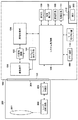
ここで、従来の一般的な撮像装置における撮像動作について説明する。図21は、従来の撮像装置の構成の一部を示す図である。図21において、撮像装置は不図示の電源スイッチがON状態になると電源部のスイッチング電源501が起動し、各ブロックに対して電源供給を行う。ユーザーにより、操作部505の一つであるレリーズボタン等が半押しされると、オートフォーカスや露出設定等の撮影のための準備動作に入る。更にレリーズボタンが押し込まれ全押し状態になると、システム制御部503がタイミング信号発生回路504や撮像素子502等の撮像系を制御し撮影動作が開始される。
Here, an image pickup operation in a conventional general image pickup apparatus will be described. FIG. 21 is a diagram showing a part of the configuration of a conventional image pickup apparatus. In FIG. 21, when a power switch (not shown) is turned on, the imaging device activates the
図22は、CMOSセンサの画素部の等価回路を示す図である。図22に示すように、フォトダイオード(以下、PD)401で発生した光キャリアをMOSトランジスタのゲート電極(フローティングディフュージョン部:FD411)に蓄積する。そして、走査回路からの駆動タイミング信号に応じて、その電位変化を増幅させて画素信号として出力する。 FIG. 22 is a diagram showing an equivalent circuit of the pixel portion of the CMOS sensor. As shown in FIG. 22, photo carriers generated in a photodiode (hereinafter, PD) 401 are accumulated in the gate electrode (floating diffusion portion: FD411) of the MOS transistor. Then, according to the drive timing signal from the scanning circuit, the potential change is amplified and output as a pixel signal.
図22に示すような画素部の等価回路を有するCMOSセンサが駆動された場合、図23のタイミングチャートに示されるように時間T2の経過後、PD401の光電荷の蓄積が終了する。そして、制御信号ΦSELがアクティブになり、行選択スイッチ(以下、TSEL)406がオンすることにより、n行目につながっている全ての画素のソースフォロア(以下、SF)410が動作状態になる。そして、画素アンプで構成されるSF410のゲートであるFD411は時間T3の期間で制御信号ΦRESがアクティブになり、リセットスイッチ(以下、TRES)403がオンとなり、SF410のゲートであるFD411はリセットされる。この際に、列出力線412にはダークレベルの信号が出力され、転送ゲート413bがオンし、ダークレベルの信号出力を信号蓄積部414に保持する。そして、この時間T3と時間T4をあわせた期間を「N読み」(ノイズ成分読み出し)期間と呼ぶ。
When the CMOS sensor having the equivalent circuit of the pixel portion as shown in FIG. 22 is driven, the accumulation of the photocharges of the
次にダークレベルの信号を信号蓄積部414へ転送する「N読み」が終了した後、時間T5の期間、制御信号ΦTXをアクティブとし転送スイッチ402をオンにすることで、PD401に蓄積されていた電荷をSF410のゲートであるFD411に転送する。ここで、制御信号ΦTSが時間T6の期間アクティブになり、転送ゲート413aがオンすることにより、PD401で蓄積された信号が信号蓄積部414に保持される。この画素信号レベルの信号出力を保持する期間を「S読み」期間と呼ぶ。そして、この信号レベルとダークレベルの差分算出動作(以下、「S−N動作」)を行うことにより、製造バラツキ等に起因する固定パターンノイズ等の影響を回避することが可能となり、通常の被写体撮影においてはS/Nの高い画像を取得することができる。
Next, after the “N reading” of transferring the dark level signal to the
しかしながら、図23の撮像素子のタイミングチャートに示される通り、「N読み」及び「S読み」動作は同時刻に実施されない。そのため、電源部のスイッチング電源501が動作する際に発生するスイッチングノイズ及びそのスイッチング電源501を構成するコイルから発生する磁界ノイズ等の影響が「N読み」及び「S読み」時に重畳されてしまう。その結果、「S−N動作」を行った際に電位レベルの差分量が行ごとに異なってしまい、これがオフセットノイズとなりS/Nが悪化してしまう。この「N読み」と「S読み」のときの電位レベルの差分量が行ごとに異なる様子を図24に示す。
However, as shown in the timing chart of the image sensor of FIG. 23, the “N reading” and “S reading” operations are not performed at the same time. Therefore, the influence of the switching noise generated when the
このような問題に対し、行ごとの「N読み」時と「S読み」時のノイズの差分量を同じにすることにより差分検出手段で横縞を低減するという技術がある。例えば特許文献1で提案されているように、動作モードに応じて複数用意された電源のスイッチング周波数の中から適切なものを選択して周波数を変更する方法が考えられる。また、特許文献2で提案されているように、電源から発生するノイズ周期を検知し、ノイズ周期に合わせて撮像素子の読み出し周期を変更する方法もある。
In order to solve such a problem, there is a technique of reducing horizontal stripes by the difference detecting means by making the difference amount of noise at the time of “N reading” and that of “S reading” for each row the same. For example, as proposed in
また、デジタルスチルカメラやデジタルビデオカメラなどの撮像装置に用いられる撮像素子は、多機能化が進んでおり、例えば、位相差方式の焦点検出機能を有するものも知られている。具体的には、撮像素子の1つの画素に2つのフォトダイオードと1つのマイクロレンズを設ける。そして、各フォトダイオードが撮影レンズの異なる瞳領域を通過した光を受光するよう構成することで、各フォトダイオードの出力信号を用いた位相差方式の焦点検出が可能となる。また、同じ画素に設けられた2つのフォトダイオードの出力信号を加算することで、画像出力を得ることができる(特許文献3参照)。 In addition, the image pickup element used in an image pickup apparatus such as a digital still camera or a digital video camera is becoming multifunctional, and for example, one having a phase difference type focus detection function is also known. Specifically, one pixel of the image sensor is provided with two photodiodes and one microlens. Then, by configuring each photodiode to receive light that has passed through different pupil regions of the taking lens, it is possible to perform phase difference focus detection using the output signal of each photodiode. Further, an image output can be obtained by adding output signals of two photodiodes provided in the same pixel (see Patent Document 3).
しかしながら、特許文献1のように周波数が選択式であると、周辺環境や部品ばらつきにより、合わせたい周波数からずれてしまったものに対しては対応できないため、周波数を変更しても最適なスイッチング周波数にならない場合がある。
However, if the frequency is of a selective type as in
特許文献2のようにノイズに合わせて読み出し周期を変更する場合、ノイズの周波数によっては読み出し周期に制限がかかってしまう。更にスイッチング電源はスイッチングのタイミングで急峻な電源電圧変動が発生する。このスイッチングのタイミングで撮像素子が「N読み」や「S読み」等の読み出し動作を実施した場合には差分量を一定にすることが出来ないため、S/Nを悪化させる可能性がある。 When the read cycle is changed according to the noise as in Patent Document 2, the read cycle is limited depending on the noise frequency. Further, in the switching power supply, a sharp power supply voltage change occurs at the timing of switching. When the image pickup device performs a read operation such as “N reading” or “S reading” at the timing of this switching, the difference amount cannot be made constant, which may deteriorate S/N.
また、特許文献3の構成では、1画素あたり2つのフォトダイオードから信号を取得する必要がある。そのため、1つの画素に1つのフォトダイオードを有する従来の構成に対して、行ごとの「S読み」のタイミングが2倍に増えてしまう。「S読み」のタイミングが2倍に増えることにより、「N読み」と一方の「S読み」のタイミングに周波数を合わせただけでは、「N読み」と2つの「S読み」時のノイズの差分量が行ごとに異なってしまい、読み出し信号の精度劣化や、画像の横縞が発生する場合がある。
Further, in the configuration of
本発明は上述した課題に鑑みてなされたものであり、その目的は、スイッチング電源に起因する画像ノイズを、より効果的に低減することができる撮像装置を提供することである。 The present invention has been made in view of the above-described problems, and an object thereof is to provide an imaging device that can more effectively reduce image noise caused by a switching power supply.
本発明に係わる撮像装置は、複数の光電変換部を有する単位画素が行列状に配置された撮像素子と、前記単位画素の複数の光電変換部から、一部の光電変換部の信号を読み出す第1の読み出し動作と、前記単位画素の複数の光電変換部から、第1の読み出し動作より多数の光電変換部の信号を読み出す第2の読み出し動作とを行う読み出し手段と、前記読み出し手段を駆動するスイッチング電源と、前記スイッチング電源のスイッチング周波数を制御する周波数制御手段と、を備え、前記周波数制御手段は、前記読み出し手段により前記複数の光電変換部からノイズ信号を読み出すタイミングと、前記複数の光電変換部から前記第1の読み出し動作により信号を読み出すタイミングと、前記複数の光電変換部から前記第2の読み出し動作により信号を読み出すタイミングとに対して、前記スイッチング周波数の位相が所定の関係になるように前記スイッチング電源のスイッチング周波数を制御することを特徴とする。 An image pickup device according to the present invention comprises: an image pickup device in which unit pixels having a plurality of photoelectric conversion units are arranged in a matrix; and a signal of a part of the photoelectric conversion units read from a plurality of photoelectric conversion units of the unit pixel. A read-out unit that performs one read-out operation and a second read-out operation that reads out signals of a larger number of photoelectric conversion units than the first read-out operation from the plurality of photoelectric conversion units of the unit pixel, and drives the read unit. A switching power supply; and a frequency control means for controlling a switching frequency of the switching power supply, wherein the frequency control means reads the noise signal from the plurality of photoelectric conversion units by the reading means, and the plurality of photoelectric conversions. So that the phase of the switching frequency has a predetermined relationship with respect to the timing of reading a signal from the unit by the first read operation and the timing of reading the signal from the plurality of photoelectric conversion units by the second read operation. In addition, the switching frequency of the switching power supply is controlled.
本発明によれば、スイッチング電源に起因する画像ノイズを、より効果的に低減することができる撮像装置を提供することが可能となる。 According to the present invention, it is possible to provide an imaging device capable of more effectively reducing image noise caused by a switching power supply.
以下、本発明の実施形態について、添付図面を参照して詳細に説明する。 Hereinafter, embodiments of the present invention will be described in detail with reference to the accompanying drawings.
<第1の実施形態>
図1は、本発明の撮像装置の第1の実施形態である撮像システムの主要部を示したブロック図である。図1において、撮像システムは、例えばレンズ交換式のデジタル一眼レフカメラからなり、カメラ本体100と、入射光を撮像素子に導くレンズユニット200とを有する。
<First Embodiment>
FIG. 1 is a block diagram showing a main part of an image pickup system which is a first embodiment of an image pickup apparatus of the present invention. In FIG. 1, the imaging system includes, for example, an interchangeable-lens digital single-lens reflex camera, and includes a
まずカメラ本体100の構成について説明する。撮像素子101には、図3に示す複数の単位画素400が格子状に配置され、撮像素子101に結像された被写体の像は、電気的な画像信号に変換されて撮像素子101から出力される。画像処理部104は、撮像素子101から出力される映像信号に対して、所定の演算処理を行う。そして、得られた映像信号に対して、画素補間処理、色変換処理、ホワイトバランス処理等の画像処理を施し、システム制御部105を介して各種表示部107に出力する。また、画像処理部104は、JPEG等の画像圧縮機能を有する。更には、撮像素子101から取得したA像信号とA+B像信号2つの情報からB像信号の生成も行う。この動作については後述する。
First, the configuration of the
AD変換回路102は撮像素子101が光電変換して出力するアナログ信号をデジタル信号に変換する。タイミング発生回路103は、画像処理部104から撮像系を駆動する基準クロック信号や制御信号を受け、撮像素子101及びAD変換回路102に対して、これらの動作タイミングを規定するクロック信号や制御信号等のタイミング信号を供給する。
The
システム制御部105は、各種演算を行うとともに、撮像素子101を含む撮像装置全体の動作を制御する。システム制御部105は、更に、画像処理部104から出力されるA像信号とB像信号の2つの光束の情報を用いて、位相差方式の焦点検出動作を行う。
The
メモリ回路106は、電気的に消去・記憶可能な不揮発性メモリも含まれ、各種パラメータやISO感度等の設定値、撮影モード及び各種補正データ等が格納されている。各種表示部107は、システム制御部105でのプログラムの実行に応じて、文字、画像、音声等の動作状態やメッセージ等を表示する液晶装置、スピーカ等を有するものであり、LCD、LED、発音素子等の組み合わせにより構成されている。また、各種表示部107の一部は光学ファインダ内等にも設けられている。
The
記録回路108は、画像データの記録または読み出しを行うための半導体メモリ等の着脱可能な記録媒体に対して読み書きを行う回路である。操作部109は、システム制御部105に各種の動作指示を入力するための操作手段である。これらの操作手段はスイッチやダイヤル、タッチパネル、視線検知によるポインティング、音声認識装置等のいずれか一つ又はそれらの組み合わせによって構成される。
The recording circuit 108 is a circuit that reads and writes a removable recording medium such as a semiconductor memory for recording or reading image data. The
モード切り替え部110は静止画撮影、ライブビュー撮影、動画撮影等の各種撮影モードを切り替え設定するためのスイッチである。電源回路111は、電池検出部、電流検出部、保護回路、DC−DCコンバータ、LDOレギュレータ等から構成されている。そして、電池装着の有無の検出機能、電池種類や残量の検出機能、過電流を検出した際には電源を遮断することにより電源回路に接続された負荷回路を保護する機能等を有する。また、システム制御部105の指示に基づき、DC−DCコンバータを制御し、所望の電源電圧を所望の期間、カメラ本体100の各部に供給する。コネクタ112,301は電源302とカメラ本体100を接続する。電源302はアルカリ電池・リチウム電池等の一次電池、Nicd電池・NiMH電池・Li電池等の2次電池、ACアダプタ等からなる。
The
次にレンズユニット200の構成について説明する。
Next, the configuration of the
撮像装置100とレンズユニット200は、レンズマウント機構113,204を介して機械的に脱着可能となっている。レンズユニット200は撮影レンズ201、レンズ駆動回路202、レンズ制御部203を備えて構成されている。レンズマウント204には、レンズユニット200をカメラ本体100と電気的に接続するコネクタも含まれ、カメラ本体100とレンズユニット200との間で、制御信号、状態信号、データ信号等を伝え合うことができる。またそのコネクタは、各種電力をカメラ本体100からレンズユニット200に供給する機能を備えている。また、コネクタは電気信号のみならず、光信号、音声信号等を伝達する構成でもよい。また、図1では、簡略化のために撮影レンズ201を一枚のレンズで示しているが、実際には多数のレンズ群から構成されている。
The
レンズ制御部203は、レンズユニット200全体を制御する。レンズ制御部203は、レンズ動作用の各種定数、変数、プログラム等を記憶するメモリを備えている。また、レンズユニット固有の情報である最大・最小絞り値、焦点距離等を保持する不揮発性メモリも備えている。また、この不揮発性メモリには、フォーカス駆動用モータや絞り駆動用モータ等のレンズユニット200に内蔵されている各種アクチュエータの駆動周波数情報等、各種設定情報が保持されている。また、レンズ制御部203は、レンズユニット200内の各回路部へ供給する電源用DC−DCコンバータ回路等も備える。
The
カメラ本体100のシステム制御部105は、撮像素子101の出力情報を用いてデフォーカス量を演算し、演算したデフォーカス量に基づいて、レンズユニット200のレンズ制御部203と通信を行う。レンズ制御部203は、レンズ駆動回路202を制御することによりピントを合わせる。また、レンズ駆動回路202は撮影時の手ブレ緩和用の振れ検知手段と手ブレ緩和用の可動式シフトレンズを駆動する制御回路等も備える。振れ検知手段により手ブレを電気信号として出力し、ブレ量の演算結果に基づいて可動式シフトレンズを移動させることにより、手ブレを低減する。
The
次に、撮像素子101で位相差検出方式の焦点検出を実現する原理について説明する。図2は、撮影レンズの射出瞳から出た光束が撮像素子が有する単位画素の1つに入射する状態を模式的に示した図である。単位画素400は、第1のフォトダイオード(以下、第1のPD)401A及び第2のフォトダイオード(以下、第2のPD)401Bを有し、カラーフィルタ402及びマイクロレンズ403により覆われている。
Next, the principle of realizing the focus detection of the phase difference detection method with the
マイクロレンズ403を有する画素に対して、撮影レンズ201の射出瞳304の中心を光軸305とする。射出瞳304を通過した光は、光軸305を中心として単位画素400に入射する。また、図2に示すように、撮影レンズの射出瞳の一部領域である瞳領域306を通過する光束はマイクロレンズ403を通して、第1のPD401Aで受光される。同様に、射出瞳304の一部領域である瞳領域307を通過する光束はマイクロレンズ403を通して、第2のPD401Bで受光される。従って、第1のPD401Aと第2のPD401Bは、それぞれ射出瞳304の別々の領域を通過した光を受光する。従って、第1のPD401Aと第2のPD401Bの信号を比較することにより、位相差の検知が可能となる。
The center of the
以下、第1のPD401Aから得られる信号をA像信号、第2のPD401Bから得られる信号をB像信号と呼ぶ。また、第1のPD401Aの信号と第2のPD401Bの信号とを加算して読み出した信号は(A+B)像信号として、撮影画像に用いることができる。
Hereinafter, the signal obtained from the
図3は、本実施形態に用いられる位相差方式の焦点検出機能を有する撮像素子101の全体構成例を示す図である。撮像素子101は、画素領域1、垂直走査回路2、読み出し回路3、水平走査回路4、出力アンプ5を含む。画素領域1には、複数の単位画素400が行列状に配置されている。ここでは、説明を分かりやすくするために4×4の16画素の配列を示しているが、実際には更に多数の単位画素が配置されている。各単位画素400は、既に説明したように、第1のフォトダイオード(以下、第1のPD)401A及び第2のフォトダイオード(以下、第2のPD)401Bを備える。垂直走査回路2は、画素領域1の画素を1行単位で選択し、選択行の画素に対して駆動信号を出力する。読み出し回路3は、列毎に列読み出し回路を備え、単位画素400からの出力信号を増幅し、その出力信号をサンプルホールドする。水平走査回路4は、読み出し回路3でサンプルホールドされた信号を列毎に順次出力アンプ5に出力するための信号を出力する。出力アンプ5は、水平走査回路4の動作により読み出し回路3から出力された信号を信号処理回路に送る。垂直走査回路2、読み出し回路3、水平走査回路4は、タイミング発生回路103からのタイミング信号により駆動される。
FIG. 3 is a diagram showing an example of the overall configuration of the
図4は、単位画素400の構成例を示す回路図である。第1のPD401A、第2のPD401Bには、第1の転送スイッチ402A、第2の転送スイッチ402Bがそれぞれ接続されている。また、第1の転送スイッチ402A及び第2の転送スイッチ402Bの出力は、フローティングディフュージョン部(以下、FD)403を通じて増幅部404に接続されている。FD403にはリセットスイッチ405が接続され、増幅部404には選択スイッチ406が接続される。
FIG. 4 is a circuit diagram showing a configuration example of the
第1のPD401A及び第2のPD401Bは、同一のマイクロレンズを通過した光を受光し、その受光量に応じた信号電荷を生成する光電変換部として機能する。第1の転送スイッチ402A及び第2の転送スイッチ402Bは、垂直走査回路2からの転送パルス信号PTXA,PTXBによって制御され、それぞれが第1のPD401A及び第2のPD401Bで発生した電荷を共通のFD403に転送する。
The
FD403は、第1のPD401A及び第2のPD401Bから転送された電荷を一時的に保持するとともに、保持した電荷を電圧信号に変換する電荷電圧変換部として機能する。増幅部404は、ソースフォロワMOSトランジスタであり、FD403に保持された電荷に基づく電圧信号を増幅して、画素信号として出力する。リセットスイッチ405は、垂直走査回路2からのリセットパルス信号PRESによって制御され、FD403の電位を基準電位VDDにリセットする。選択スイッチ406は、垂直走査回路2からの制御信号PSELによって制御され、増幅部404で増幅された画素信号を列出力線407に出力する。
The
図5は、図3の読み出し回路3の1列分の構成例を示す回路図である。読み出し回路3は、列毎に図5に示す構成の回路を備えるが、各列の構成は共通であるので、図5では1列分のみ示している。列出力線407上の信号電圧はオペアンプ408により増幅される。オペアンプ408には基準電圧VREFが供給される。オペアンプ408の入力にはクランプ容量C0が接続され、入出力間にはフィードバック容量Cfが接続される。また、フィードバック容量Cfの両端には、両端をショートさせるためのスイッチ409が設けられ、スイッチ409は、読み出し回路3の制御信号PC0Rで制御される。列出力線407には定電流源410が接続されている。
FIG. 5 is a circuit diagram showing a configuration example of one column of the read
容量CTS_A+B,CTS_A,CTNは、オペアンプ408からの信号電圧を保持するための容量である。スイッチ411,412,413は、それぞれ容量CTS_A+B,CTS_A,CTNへの書き込みを制御するスイッチである。スイッチ411は、制御信号PTS_A+Bで制御され、スイッチ412は、制御信号PTS_Aで制御され、スイッチ413は、制御信号PTNで制御される。
The capacitors CTS_A+B, CTS_A, and CTN are capacitors for holding the signal voltage from the
容量CTS2,CTN2は、容量CTS_A+B,CTS_A,CTNからの信号電圧を保持するための容量である。スイッチ414,415,416は、容量CTS2,CTN2への書き込みを制御するスイッチである。スイッチ414は、容量CTS_A+Bの信号を容量CTS2に書き込むためのスイッチで、制御信号PTS2_A+Bで制御される。スイッチ415は、容量CTS_Aの信号を容量CTS2に書き込むためのスイッチで、制御信号PTS2_Aで制御される。スイッチ416は、容量CTNの信号を容量CTN2に書き込むためのスイッチで、制御信号PTN2で制御される。
The capacitors CTS2 and CTN2 are capacitors for holding the signal voltages from the capacitors CTS_A+B, CTS_A and CTN. The
また、容量CTS2,CTN2の直前には、バッファとしてのボルテージフォロワ417,418,419が設けられている。ボルテージフォロワ417,418,419は、容量CTS_A+B,CTS_A,CTNのそれぞれに蓄積された電位と等しい電位を、容量分割によらず容量CTS2,CTN2に伝達する。
Immediately before the capacitors CTS2 and CTN2,
スイッチ420,421は、水平走査回路4からの制御信号PHで制御され、容量CTS2に書き込まれた信号は共通出力線422を介して、容量CTN2に書き込まれた信号は共通出力線423を介して、それぞれ出力アンプ5に出力される。なお、容量CTS_A+B,CTS_A,CTNへの信号書き込みと、容量CTS2,CTN2からの水平走査による信号読み出しは、並行して行われる。
The
図6は、撮像素子101の駆動タイミングチャートを示す図である。時刻t1において、水平同期信号SYNCが立ち上がるとともに、選択された行の制御信号PSELがLからHとなる。これにより選択された行の選択スイッチ406がオンし、選択された行の画素信号を列出力線407に出力することが可能となる。
FIG. 6 is a diagram showing a drive timing chart of the
時刻t2では、リセットパルス信号PRESがLからHとなり、リセットスイッチ405がオンし、FD403の電位が電源VDDにリセットされる。時刻t3では、リセットパルス信号PRESがHからLとなり、リセットスイッチ405がオフし、FD403のリセットが解除される。このときのFD403の電位は、列出力線407に増幅部404を介してリセット信号レベルとして読み出され、読み出し回路3に入力される。読み出し回路3では、制御信号PC0RがHでスイッチ406がオンになっており、オペアンプ403が基準電圧VREFの出力をバッファする状態でリセット信号レベルがクランプ容量C0に入力される。
At time t2, the reset pulse signal PRES changes from L to H, the
その後、時刻t4で制御信号PCORをHからLとし、時刻t5で制御信号PTNをHにしてスイッチ413をオンして、そのときのオペアンプ408の出力をリセット電圧として容量CTNへ書き込む。その後、時刻t6で制御信号PTNをLとして、スイッチ413をオフして容量CTNへのリセット電圧の書き込みを終了する。この時刻t5から時刻t6までの期間を「N読み」(ノイズ成分読み出し)期間と呼ぶ。
After that, the control signal PCOR is changed from H to L at time t4, the control signal PTN is changed to H at time t5, and the
「N読み」が終了した後、時刻t7で制御信号PTS_AをHとし、スイッチ412をオンにし、容量CTS_Aに信号を書き込み可能な状態とする。続いて、時刻t8で転送パルス信号PTXAをHとして、第1のPD401Aの電荷をFD403へ転送し、時刻t9で転送パルス信号PTXAをLとする。この動作により、第1のPD401Aに蓄積された電荷がFD403へ読み出される。そして、FD403の電位の変化に応じた出力が増幅部404及び列出力線407を介して読み出し回路3へ供給される。読み出し回路3では、オペアンプ408がクランプ容量C0とフィードバック容量Cfの比率に応じた利得で列出力線407から供給された電圧を増幅して出力する。この第1のPD401Aから提供された信号電圧は、容量CTS_Aに書き込まれる。時刻t10で制御信号PTS_AをHからLと切り替え、スイッチ412をオフし、容量CTS_Aへの書き込みを終了する。この時刻t7から時刻t10までの第1のPD401Aに蓄積された信号を読み出す期間を「S_A読み」(A像信号読み出し)期間と呼ぶ。
After the “N reading” is completed, at time t7, the control signal PTS_A is set to H, the
時刻t11で制御信号PTS_A+BをHとし、スイッチ411をオンにし、容量CTS_A+Bに信号を書き込み可能な状態とする。続いて、時刻t12で再び転送パルス信号PTXAをHとすると同時に転送パルス信号PTXBもHとする。この動作により、第1のPD401Aと第2のPD401Bの双方の電荷を同時にFD403へ読み出すことができる。そして、時刻t14で転送パルス信号PTXA及びPTXBをLとする。FD403に読み出された電荷は、増幅部404により電圧に変換され、列出力線407を介して読み出し回路3へ供給され、オペアンプ408で増幅される。オペアンプ408により増幅された信号は容量CTS_A+Bに書き込まれる。時刻t16で制御信号PTS_A+BをHからLに切り替え、スイッチ411をオフし、容量CTS_A+Bへの書き込みを終了する。この時刻t11から時刻t16までの第1のPD401A及び第2のPD401Bに蓄積された信号を読み出す期間を「S_A+B読み」(A+B像信号読み出し)期間と呼ぶ。以上の動作により、容量CTSN,CTS_A,CTS_A+Bへの信号書き込みが完了する。
At time t11, the control signal PTS_A+B is set to H, the
なお、時刻t12では転送パルス信号PTXA及びPTXBを同時にHとしたが、転送パルス信号PTXBだけをHとして第2のPD401Bの電荷をFD403へ転送してもよい。この場合、第1のPD401Aの電荷がすでにFD403へ転送されているので、第1のPD401A及び第2のPD401Bの電荷を加算した出力を得ることができる。
Note that at time t12, the transfer pulse signals PTXA and PTXB are set to H at the same time, but only the transfer pulse signal PTXB may be set to H to transfer the electric charge of the
時刻t17では制御信号PCORを再びHとし、スイッチ406がオンし、読み出し回路3では、オペアンプ403が基準電圧VREFの出力をバッファする状態に戻る。そして時刻t18で垂直選択パルス信号PSELをLとし、選択されていた行の画素からの信号の読み出しを終了し、選択されていた行は列出力線407から切り離される。その後、時刻t19で水平同期信号SYNCが再び立ち上がり、同時に次行の垂直選択パルス信号PSELがHとなり、次行の画素の選択が開始される。
At time t17, the control signal PCOR is set to H again, the
また、(A+B)像信号の容量CTS_A+Bへの書き込みと平行して、時刻t12において、制御信号PTS2_Aと制御信号PTN2をLからHとし、スイッチ415及びスイッチ416をオンする。容量CTNに保持された信号はボルテージフォロワ419を介して、容量CTN2へ書き込まれ、容量CTS_Aに保持された信号はボルテージフォロワ418を介して容量CTS2に書き込まれる。そして、時刻t13で制御信号PTN2及び制御信号PTS2_Aが同時にHからLとなり、容量CTN2及び容量CTS2への書き込みが終了する。
Further, in parallel with the writing of the (A+B) image signal to the capacitor CTS_A+B, at time t12, the control signal PTS2_A and the control signal PTN2 are changed from L to H, and the
その後、時刻t13〜t15の間に、水平走査回路4の駆動パルスPHが各列の読み出し回路毎に順次L→H→Lとなる。それに伴い、列毎にスイッチ420,421がオフ→オン→オフとなり、水平走査が行われる。スイッチ420,421がオフ→オン→オフとなったときに各列の容量CTS2,CTN2に保持された信号は共通出力線422,423へそれぞれ読み出され、出力アンプ5で共通出力線422,423の信号の差電圧として出力される。この差電圧がA像信号となる。この画素信号レベルとノイズ信号レベルの差分電圧算出動作(以下、「S−N」動作)を行うことにより、製造バラツキ等に起因する固定パターンノイズ等の影響を回避することが可能となり、S/Nの高い画像を取得することが出来る。なお、共通出力線422,423は各列の信号を読み出す毎に不図示のリセットスイッチにより基準電位にリセットされる。
After that, the driving pulse PH of the horizontal scanning circuit 4 sequentially becomes L→H→L for each reading circuit in each column between times t13 and t15. Along with this, the
ここで、A像信号の水平走査は、(A+B)像信号の容量CTS_A+Bへの書き込み中(TA+Bの期間)に行われる。この水平走査期間は、容量CTS_A+Bへの書き込みが終わる時刻t16までに完了する。(A+B)像信号の容量CTS_A+Bへの書き込みが終わった後、(A+B)像信号の容量CTS2の書き込み及び水平走査が行われる。これらの動作は次行のFD403のリセット、容量CTN及びCTS_Aへの書き込みと並行して行われる。時刻t17では、制御信号PTN2及び制御信号PTS2_A+Bを同時にLからHとすることで、スイッチ414,416がオンする。容量CTNに保持された信号はボルテージフォロワ419を介して、容量CTN2へ書き込まれる。さらに、容量CTS_A+Bに保持された信号はボルテージフォロワ417を介して、容量CTS2に書き込まれる。そして、時刻t18で制御信号PTN2及び制御信号PTS2_A+Bが同時にHからLとなり、書き込みが終了する。
Here, the horizontal scanning of the A image signal is performed during the writing of the (A+B) image signal into the capacitor CTS_A+B (TA+B period). This horizontal scanning period is completed by time t16 when writing to the capacitor CTS_A+B ends. After the writing of the (A+B) image signal in the capacitor CTS_A+B is completed, the writing and horizontal scanning of the (A+B) image signal in the capacitor CTS2 are performed. These operations are performed in parallel with resetting of the
その後、容量CTN2、CTS2に保持された信号は時刻t18〜時刻t20の間に、水平走査回路4の駆動パルスPHが順次L→H→Lとなることで水平走査が行われる。駆動パルスPHにより各列のスイッチ420,421が駆動されてオフ→オン→オフする。スイッチ420,421により列毎の容量CTS2,CTN2に保持された信号は共通出力線422,423へそれぞれ読み出され、出力アンプ5で共通出力線422,423の差電圧として出力される。この差電圧が(A+B)像信号となる。
After that, the signals held in the capacitors CTN2 and CTS2 are horizontally scanned by the drive pulse PH of the horizontal scanning circuit 4 sequentially changing from L→H→L between time t18 and time t20. The drive pulse PH drives the
ここで、(A+B)像信号の水平走査は、次行のFD403のリセット及び、容量CTN,CTS_Aへの書き込みと並行して行われる。並行して行うことにより処理時間を短縮できる。この水平走査期間は、次行の容量CTS_Aへの書き込みが終わる次の時刻t20までに完了できる。
Here, the horizontal scanning of the (A+B) image signal is performed in parallel with resetting of the
このようにして読み出されたA像信号から撮影レンズの瞳の一部を透過する光束の情報が得られ、さらに(A+B)像信号とA像信号の差分をとることにより、第2のPD401Bからの出力信号であるB像信号(A像の光電変換部以外の信号)を得ることができる。このB像信号からは、A像信号とは異なる瞳領域を透過した光束の情報が得られる。従って、これらA像信号とB像信号との2つの光束の情報から位相差を算出し、被写体の焦点情報や距離情報を得ることができる。 Information of the light flux that passes through a part of the pupil of the photographing lens is obtained from the A image signal read in this way, and the difference between the (A+B) image signal and the A image signal is obtained. It is possible to obtain a B image signal (a signal other than the photoelectric conversion unit for the A image) which is the output signal from the. From this B image signal, information on the light flux that has passed through the pupil region different from that of the A image signal can be obtained. Therefore, the phase difference can be calculated from the information of the two light fluxes of the A image signal and the B image signal, and the focus information and distance information of the subject can be obtained.
ところで、図6の撮像素子のタイミングチャートに示される通り、位相差方式の焦点検出機能を有する撮像素子の「N読み」、「S_A読み」及び「S_A+B読み」動作は同時刻に実施されない。そのため、電源部に図21に示したような従来の電源部を用いると次のような問題が起こる。 By the way, as shown in the timing chart of the image sensor of FIG. 6, the “N read”, “S_A read” and “S_A+B read” operations of the image sensor having the phase difference type focus detection function are not performed at the same time. Therefore, if the conventional power supply unit as shown in FIG. 21 is used as the power supply unit, the following problems occur.
即ち、図21の電源部のスイッチング電源501が動作する際に発生するスイッチングノイズ又はスイッチング電源501を構成するコイルから発生する磁界ノイズ等の影響が撮像素子の「N読み」、「S_A読み」及び「S_A+B読み」時に重畳される。重畳された場合、S−N動作した際に電位レベルの差分量がA像及びA+B像の間で、更には行ごとに異なってしまうため、これがオフセットノイズとなりS/Nが悪化してしまう。このS/Nの悪化は撮影画像の画像ノイズ発生や焦点検出精度低下等に影響を与える。この「N読み」、「S_A読み」及び「S_A+B読み」時の電位レベルの差分量が読み出しタイミングごとに異なっている様子を図7に示す。
That is, the influence of switching noise generated when the switching
以下では、上記の問題点を解決する手法について説明する。図8は、本実施形態における電源部と撮像装置の構成の一部を示す概要図である。図8において、電源回路111は、スイッチング素子の制御により入力電圧を異なる値の出力電圧に変換するスイッチング電源601、位相補正部602、周波数制御部603を備えて構成され、電源回路111からの出力は、撮像素子101等に供給される。
Hereinafter, a method for solving the above problems will be described. FIG. 8 is a schematic diagram showing a part of the configuration of the power supply unit and the image pickup apparatus in this embodiment. 8, the
図11は本実施形態における撮像動作を示すフローチャートである。図8および図11を用いて、本実施形態の撮像装置における撮像動作の一連の流れについて説明する。 FIG. 11 is a flowchart showing the image pickup operation in this embodiment. A series of flow of the image pickup operation in the image pickup apparatus according to the present embodiment will be described with reference to FIGS. 8 and 11.
S901で電源スイッチにより撮像装置が起動された後、本撮影動作に移行するまでは撮像素子101等の撮像系には電源供給を行わない待機状態となる。S902では、ユーザーは、モード切り替え部110により、静止画撮影、動画撮影、ライブビュー撮影等の撮影モードを選択可能である。選択された撮影モードが、位相差方式の焦点検出を行う動画撮影やライブビュー撮影モードの場合はS903に進み、そうでない場合はS920に進む。
After the image pickup apparatus is started by the power switch in S901, the image pickup system such as the
S903では、システム制御部105は周波数制御部603に対して、位相差方式の焦点検出を行う場合の撮像素子101の読み出し周期に基づいて決定される周波数情報606を送る。そして、周波数制御部603は、この周波数情報606に基づき、撮像系の基準クロック608から生成する第1及び第2のスイッチングパルスの周波数をそれぞれ第1の駆動周波数fsw1及び第2の駆動周波数fsw2に設定する。第1の駆動周波数fsw1及び第2の駆動周波数fsw2は、撮像素子101の「N読み」、「S_A読み」及び「S_A+B読み」のタイミングと下記の関係になるように設定される。
In step S903, the
まず、第1の駆動周波数fsw1について、図12も参照して説明する。この第1の駆動周波数fsw1は、撮像素子101の「N読み」タイミングから「S_A読み」タイミングまでの期間をΔt1、スイッチング電源601が駆動可能なスイッチング周波数に逓倍する整数をK1として、以下の式(1)で表わされる。
First, the first drive frequency fsw1 will be described with reference to FIG. This first drive frequency fsw1 is given by the following equation, where Δt1 is the period from the “N reading” timing to the “S_A reading” timing of the
fsw1=K1/Δt1 …(1)
Δt1:「N読み」から「S_A読み」までの期間
K1:電源ICが駆動可能なスイッチング周波数に逓倍する整数
次に第2の駆動周波数fsw2について、図12も参照して説明する。この第2の駆動周波数fsw2は、撮像素子101の「S_A読み」タイミングから「S_A+B読み」タイミングまでの期間をΔt2、スイッチング電源601が駆動可能なスイッチング周波数に逓倍する整数をK2として、以下の式(2)で表わされる。
fsw1=K1/Δt1 (1)
Δt1: Period from “N reading” to “S_A reading” K1: Integer that is multiplied by the switching frequency that can be driven by the power supply IC Next, the second driving frequency fsw2 will be described with reference to FIG. 12. This second drive frequency fsw2 is expressed by the following equation, where Δt2 is the period from the “S_A reading” timing to the “S_A+B reading” timing of the
fsw2=K2/Δt2 …(2)
Δt2:「S_A読み」から「S_A+B読み」までの期間
K2:電源ICが駆動可能なスイッチング周波数に逓倍する整数
ここで、周波数制御部603は、例えば位相同期回路(PLL)701,704を用いて、図9に示すように構成されている。位相同期回路701,704の出力部には、分周用分周器702,705、入力部には逓倍用分周器703,706が配置されている。撮像系の基準クロック608を周波数情報606に基づいて、所望の分周比で分周させることにより、Δt1及びΔt2の期間に同期した逓倍周波数でスイッチング電源601の駆動周波数を生成することが可能である。
fsw2=K2/Δt2 (2)
Δt2: Period from “S_A reading” to “S_A+B reading” K2: Integer that is multiplied by the switching frequency that the power supply IC can drive Here, the
図11の説明に戻り、S904では、撮影開始スイッチをONすることにより、ライブビュー撮影動作が開始される。S905では、システム制御部105はスイッチング電源601に対して、撮像系の電源供給を指示する電源制御信号607を送る。そして、電源制御信号607を受け取ったスイッチング電源601は、初期設定された所定の駆動周波数で撮像素子101に電源供給を行い、撮像素子101が初期化される。
Returning to the description of FIG. 11, in S904, the live view shooting operation is started by turning on the shooting start switch. In step S<b>905, the
S906では、システム制御部105は、周波数制御部603に対して、撮像系の基準クロック608を送る。周波数制御部603は、S903で設定した周波数情報に基づき、撮像系の基準クロック608を第1及び第2のスイッチングパルス605,613に変換する。周波数制御部603から出力される第1及び第2のスイッチングパルス605,613は位相補正部602に入力される。位相補正部602は、第1行目読み出し時において、位相補正制御動作すること無く、スイッチング電源601に対して、第1及び第2のスイッチングパルス605,613を入力する。そして、スイッチング電源601は、第1のスイッチングパルス605の第1の駆動周波数fsw1で駆動を開始し、撮像素子101に対して電源供給を行う。
In step S906, the
S907では、システム制御部105は、タイミング信号発生回路103に対して、撮像系の基準クロック、水平走査信号、垂直走査信号等の撮像系制御信号を送り、撮像素子101の画像読み出し動作を開始する。S908で「S_A読み」が終了すると、S909では、スイッチング電源601の駆動周波数を第2のスイッチングパルス605の第2の駆動周波数fsw2に変更する。そして、S910で「S_A+B読み」を終了する。
In step S<b>907, the
S911では、位相検出部604は、スイッチング電源601の第1のスイッチングパルス605と撮像素子101の「S_A読み」の読み出しパルス611の位相差Δn1を算出する。更には、スイッチング電源601の第2のスイッチングパルス613と撮像素子101の「S_A+B読み」の読み出しパルス612の位相差Δn2を算出する。
In S911, the
その後、S912では、位相検出部604は次行の読み出しタイミングでの位相差(Δm1,Δm2)を予測演算する。ΔmxはΔmx=Δnx±αx(xは1又は2を表わす)となる関係で表わされるパラメータである。ここで、αxとはスイッチング電源601の第1のスイッチングパルス605と撮像素子101の「S_A読み」の読み出しパルス611、及び第2のスイッチングパルス613と「S_A+B読み」の読み出しパルス612に発生する行ごとの位相ズレ量を表わすパラメータである。スイッチング電源601のスイッチング周期が撮像素子101の水平走査信号の周期の整数倍でない場合に、行ごとに両者の位相関係にαxのズレが発生する。そのため、上記の演算を行うことにより、次行の読み出しタイミングでの位相差(Δmx)を予測することが可能となる。
After that, in step S912, the
そして、S913では、|Δnx−Δmx|=αx≦Aの関係になるか否かの判定を行う。ここでAとは行ごとの位相ズレ量αxに対して、周辺環境やハードウェアを構成する部品の製造ばらつき等による、周波数精度ばらつきの影響を加味した値とする。上記の関係式が成り立たない場合には、次行でスイッチング電源601の第1及び第2のスイッチングパルス605,613と撮像素子101の「S_A読み」及び「S_A+B読み」の読み出しパルス611,612が重畳することが無い。そのため、S914をスキップし、S915に移行する。一方、上記の関係が成り立つ場合には両者が重畳する可能性があるため、S914に移行し、位相検出部604は位相補正部602に対して、位相補正量分位相をシフトさせる位相補正情報609を送る。位相補正部602は第1又は第2のスイッチングパルス605,613の位相補正を行う。
Then, in S913, it is determined whether or not the relationship of |Δnx−Δmx|=αx≦A is satisfied. Here, A is a value in which the influence of the frequency accuracy variation due to the peripheral environment or the manufacturing variation of the components constituting the hardware is added to the phase shift amount αx for each row. If the above relational expression does not hold, the first and
ここで、位相補正部602は、例えば、複数の遅延回路801とセレクタ802を用いて図10に示されるように構成される。位相補正部602は、位相検出部604から受け取った位相補正情報609に基づきセレクタ802でどの遅延回路801の信号を出力させるかを決定することにより、位相補正部602の入力パルスの位相補正を行う。ここで、入力パルスとは周波数制御部603の出力パルスとする。また、この位相補正部602での位相補正量Δsは、例えばスイッチング電源601のスパイク幅分以上ずらせばよいものとする。このように制御することにより、撮像素子101の各信号読み出しタイミングとスイッチングタイミングとが重畳しないように制御することが出来る。そのため、スイッチング電源601のスイッチングタイミングで発生する急峻な電源電圧変動の影響を回避することが可能となる。
Here, the
そして、S915では、全行の読み出しが完了したか否かの判定を行う。全行の読み出しが完了していない場合には、S916でスイッチング電源601の駆動周波数を第1の駆動周波数fsw1に変更し、S908に戻り同様の処理を行う。全行の読み出しが終了した場合にはS917に移行する。
Then, in S915, it is determined whether the reading of all rows is completed. If the reading of all rows is not completed, the drive frequency of the switching
S917では、電源スイッチをオフするか否かの判定を行い、電源スイッチをオフしない場合にはS919に移行し、撮影モードを変更するか否かの判定を行う。変更しない場合には、S904の撮影開始スイッチのオンを検知する状態に戻り、撮影モードを変更する場合には、S902の撮影モードを選択する状態に戻る。S917において、電源スイッチをオフする場合にはS918に移行し、撮像装置の電源がオフされる。 In S917, it is determined whether or not the power switch is turned off. If the power switch is not turned off, the process proceeds to S919, and it is determined whether or not the photographing mode is changed. If not changed, the state returns to the state of detecting the ON of the photographing start switch in S904, and if the photographing mode is changed, the state returns to the state of selecting the photographing mode of S902. In S917, when the power switch is turned off, the process proceeds to S918, and the power of the image pickup apparatus is turned off.
一方、S902において、モード切り替え部110で選択された撮影モードが、位相差方式の焦点検出を行わない動画撮影モード、ライブビュー撮影モード、静止画撮影モードであった場合、S920に進む。
On the other hand, in S902, when the shooting mode selected by the
S920では、システム制御部105は、周波数制御部603に対して、位相差方式の焦点検出を行わない動画撮影やライブビュー撮影や静止画撮影時の撮像読み出し周期に基づいて決定される周波数情報606を送る。そして、周波数制御部603は、この周波数情報606に基づき、撮像系の基準クロック608から生成する第3のスイッチングパルスの周波数を第3の駆動周波数fsw3に設定する。この第3の駆動周波数fsw3は、撮像素子101の「N読み」、「S_A+B読み」のタイミングと下記関係になるように設定される。
In step S<b>920, the
駆動周波数fsw3は、撮像素子101の「N読み」のタイミングから「S_A+B読み」のタイミングまでの期間をΔt3、スイッチング電源601が駆動可能なスイッチング周波数に逓倍する任意整数をK3として、以下の式(3)で表わされる。
The driving frequency fsw3 is expressed by the following formula (3), where Δt3 is the period from the “N reading” timing of the
fsw3=K3/Δt3 …(3)
Δt3:「N読み」から「S_A+B読み」までの期間
K3:電源ICが駆動可能なスイッチング周波数に逓倍する整数
S921では、撮影開始スイッチをONすることにより、撮影動作が開始される。S922では、システム制御部105は、スイッチング電源601に対して、撮像系の電源供給を指示する電源制御信号607を送る。そして、電源制御信号607を受け取ったスイッチング電源601は、初期設定された所定の駆動周波数で撮像素子101に電源供給を行い、記撮像素子101が初期化される。
fsw3=K3/Δt3 (3)
Δt3: Period from “N reading” to “S_A+B reading” K3: Integer that is multiplied by the switching frequency at which the power supply IC can be driven In S921, the shooting operation is started by turning on the shooting start switch. In step S922, the
S923では、システム制御部105は、周波数制御部603に対して、撮像系の基準クロック608を送り、周波数制御部603は、S920で設定した周波数情報に基づき、撮像系の基準クロック608を第3のスイッチングパルス614に変換する。周波数制御部603から出力される第3のスイッチングパルス614は、位相補正部602に入力される。位相補正部602は、第1行目読み出し時において、位相補正制御動作すること無く、スイッチング電源601に対して、第3のスイッチングパルス614を入力する。そして、スイッチング電源601は、第3のスイッチングパルスの第3の駆動周波数fsw3で駆動を開始し、撮像素子101に対して電源供給を行う。
In S923, the
S924では、システム制御部105は、タイミング信号発生回路103に対して、撮像系の基準クロック、水平走査信号、垂直走査信号等の撮像系制御信号を送る。S925では、位相検出部604は、スイッチング電源601の第3のスイッチングパルス614と撮像素子101の「S_A+B読み」の読み出しパルス612の位相差Δn3を算出する。
In step S924, the
その後、S926では、位相検出部604は次行の読み出しタイミングでの位相差Δm3を予測演算する。Δm3は、Δm3=Δn3±α3となる関係で表わされるパラメータである。ここで、α3とは、スイッチング電源601の第3のスイッチングパルス614と撮像素子101の「S_A+B読み」の読み出しパルス612が発生する行ごとの位相ズレ量を表わすパラメータである。スイッチング電源601のスイッチング周期が撮像素子101の水平走査信号の周期の整数倍でない場合に、行ごとに両者の位相関係にα3のズレが発生する。そのため、上記の演算を行うことにより、次行の読み出しタイミングでの位相差Δm3を予測することが可能となる。
After that, in S926, the
そして、S927では、|Δn3−Δm3|=α3≦Aの関係になるか否かの判定を行う。上記の関係式が成り立たない場合には、次行でスイッチング電源601の第3のスイッチングパルス614と撮像素子101の「S_A+B読み」の読み出しパルス612とが重畳することが無い。そのため、S928をスキップし、S929に移行する。一方、上記の関係が成り立つ場合には両者が重畳する可能性があるため、S928に移行する。そして、位相検出部604は、位相補正部602に対して、位相補正量分位相をシフトさせる位相補正情報609を送り、位相補正部602は第3のスイッチングパルス614の位相補正を行う。
Then, in S927, it is determined whether or not the relationship of |Δn3−Δm3|=α3≦A is satisfied. When the above relational expression is not established, the third switching pulse 614 of the switching
そして、S929では、全行の読み出しが完了したか否かの判定を行う。まだ、全行の読み出しが完了していない場合には、S925に戻り、同様の処理を行う。全行の読み出しが終了した場合にはS930に移行する。 Then, in S929, it is determined whether reading of all rows is completed. If all rows have not been read yet, the process returns to S925 and the same process is performed. When the reading of all rows is completed, the process proceeds to S930.
S930では、電源スイッチをオフするか否かの判定を行い、電源スイッチをオフしない場合には、S931に移行し、撮影モードを変更するか否かの判定を行う。変更しない場合には、S921の撮影開始スイッチのオンを検知する状態に戻り、撮影モードを変更する場合には、S902の撮影モードを選択する状態に戻る。S930において、電源スイッチをオフする場合にはS918に移行し、撮像装置の電源がオフされる。 In S930, it is determined whether or not the power switch is turned off. If the power switch is not turned off, the process proceeds to S931 and it is determined whether or not the photographing mode is changed. If not changed, the state returns to the state of detecting the ON of the photographing start switch in S921, and if the photographing mode is changed, the state returns to the state of selecting the photographing mode of S902. In S930, when the power switch is turned off, the process proceeds to S918, and the power of the image pickup apparatus is turned off.
図12は、本実施形態の周波数制御を行うことにより、「N読み」、「S_A読み」及び「S_A+B読み」タイミングの、スイッチング電源のスイッチングタイミングに対する位相関係が全て同じである様子を示した図である。本実施形態では、図12のように、撮像系の基準クロックを元に、周波数制御部で撮像素子の「N読み」タイミングと「S_A読み」タイミングの期間Δt1に同期した第1の駆動周波数を生成する。また、同様に「S_A読み」タイミングと「S_A+B読み」タイミングの期間Δt2に同期した第2の駆動周波数を生成する。そして、所定のタイミングでスイッチング電源の駆動周波数を切り替えることにより、撮像素子の全ての読み出しタイミングが、スイッチング電源のスイッチングタイミングとの位相関係が同じになるようにする。 FIG. 12 is a diagram showing a state in which the phase relationships of the “N reading”, “S_A reading”, and “S_A+B reading” timing with respect to the switching timing of the switching power supply are all the same by performing the frequency control of the present embodiment. Is. In the present embodiment, as shown in FIG. 12, the first drive frequency synchronized with the period Δt1 of the “N reading” timing and the “S_A reading” timing of the image pickup device is set by the frequency control unit based on the reference clock of the image pickup system. To generate. Similarly, the second drive frequency synchronized with the period Δt2 of the “S_A read” timing and the “S_A+B read” timing is generated. Then, by switching the drive frequency of the switching power supply at a predetermined timing, all read timings of the image pickup device have the same phase relationship with the switching timing of the switching power supply.
以上のように、撮像素子の動作に合わせてスイッチング電源の駆動周波数を制御することにより、撮像素子の「N読み」、「S_A読み」及び「S_A+B読み」タイミングに対して、スイッチング電源のスイッチングタイミングとの位相関係を全て同じにすることが出来る。そのため、「N読み」、「S_A読み」、「S_A+B読み」の電位レベルの差分量を等しくすることが可能となる。その結果、撮影画像に対するスイッチング電源に起因するノイズの影響を抑え、読み出し信号の精度向上を図ることができ、撮影画像に現れる横縞ノイズを低減することができる。 As described above, by controlling the drive frequency of the switching power supply in accordance with the operation of the image pickup device, the switching timing of the switching power supply is changed with respect to the “N reading”, “S_A reading”, and “S_A+B reading” timing of the image pickup device. Can have the same phase relationship with. Therefore, it is possible to make the difference amounts of the potential levels of “N reading”, “S_A reading”, and “S_A+B reading” equal. As a result, it is possible to suppress the influence of noise caused by the switching power supply on the captured image, improve the accuracy of the read signal, and reduce the horizontal stripe noise appearing in the captured image.
なお、本実施形態では、行毎にスイッチング電源のスイッチングパルスと撮像素子の読み出しパルスの位相差を検出したが、本発明はこれに限定されるものでは無い。例えば、1行目の読み出しタイミングのみ検出し、スイッチング電源のスイッチング周波数及び水平走査信号の周期などから、何行目の読み出し時にスイッチングと重畳する可能性があるか判断し、重畳する行のみ補正してもよい。また、この時のスイッチング周波数はパルス検出部において検出したスイッチングパルスから算出しても良い。 In the present embodiment, the phase difference between the switching pulse of the switching power supply and the read pulse of the image sensor is detected for each row, but the present invention is not limited to this. For example, only the read timing of the first row is detected, and based on the switching frequency of the switching power supply, the period of the horizontal scanning signal, etc., it is determined which row is likely to overlap with the switching, and only the overlapped row is corrected. May be. Further, the switching frequency at this time may be calculated from the switching pulse detected by the pulse detection unit.
<第2の実施形態>
以下、本発明の第2の実施形態について説明する。この第2の実施形態では、撮像装置の構成は、図1で説明した第1の実施形態と同様であるため、第1の実施形態と同様の部分については説明を省略し、異なる部分についてのみ説明する。なお、第2の実施形態では、電源回路が第1の実施形態と異なるため、第1の実施形態における電源回路111を電源回路111Aと表記する。
<Second Embodiment>
The second embodiment of the present invention will be described below. In the second embodiment, the configuration of the image pickup apparatus is similar to that of the first embodiment described with reference to FIG. explain. In the second embodiment, since the power supply circuit is different from that of the first embodiment, the
図13は、第2の実施形態における電源部と撮像装置の構成の一部を示す概要図である。図13において、電源回路111Aは、スイッチング素子の制御により入力電圧を異なる値の出力電圧に変換するスイッチング電源1601、周波数制御部1602を備えて構成され、電源回路111Aからの出力は、撮像素子101等に供給される。
FIG. 13 is a schematic diagram showing a part of the configuration of the power supply unit and the imaging device according to the second embodiment. 13, the power supply circuit 111A includes a switching
図16は、本実施形態における撮像動作を示すフローチャートである。図13および図16を用いて、本実施形態の撮像動作の一連の流れについて説明する。 FIG. 16 is a flowchart showing the imaging operation in this embodiment. A series of flow of the imaging operation of this embodiment will be described with reference to FIGS. 13 and 16.
S1901で電源スイッチにより撮像装置が起動された後、本撮影動作に移行するまでは撮像素子101等の撮像系には電源供給を行わない待機状態となる。S1902では、ユーザーは、モード切り替え部110により、静止画撮影、動画撮影、ライブビュー撮影等の撮影モードを選択可能である。選択された撮影モードが、位相差方式の焦点検出を行う動画撮影モードやライブビュー撮影モードの場合は、S1903に進み、そうでない場合はS1920に進む。
After the image pickup apparatus is started by the power switch in S1901, the image pickup system such as the
S1903では、システム制御部105は周波数制御部1602に対して、位相差方式の焦点検出を行う動画撮影やライブビュー撮影時の撮像読み出し周期に基づいて決定される周波数情報を送る。そして、周波数制御部1602はこの周波数情報に基づき、出力周波数を撮像読み出し周期の逓倍周波数になるように設定する。
In step S1903, the
ここで、撮像読み出しタイミング信号に同期するスイッチング周波数をfswとする。「N読み」タイミングから「S_A読み」タイミングまでのサンプリング周期Δt1と、その逆数から求められる周波数をf1とする。また、「N読み」タイミングから「S_A+B読み」タイミングまでのサンプリング周期Δt2と、その逆数から求められる周波数をf2とする。周波数f1とf2との最小公倍数を周波数f3、電源ICが駆動可能なスイッチング周波数に逓倍する整数をK1として、スイッチング周波数fswは以下の式(4)を満足する値に設定する。 Here, the switching frequency synchronized with the imaging read timing signal is fsw. The sampling period Δt1 from the “N reading” timing to the “S_A reading” timing and the frequency obtained from its reciprocal are f1. Further, the sampling period Δt2 from the “N reading” timing to the “S_A+B reading” timing and the frequency obtained from the reciprocal thereof are f2. The least common multiple of the frequencies f1 and f2 is set to the frequency f3, and an integer that multiplies the switching frequency at which the power supply IC can be driven is set to K1, and the switching frequency fsw is set to a value that satisfies the following expression (4).
fsw=f3 ×K1 …(4)
f1=1/Δt1
f2=1/Δt2
f3:f1とf2との最小公倍数
K1:電源ICが駆動可能なスイッチング周波数に逓倍する整数
スイッチング周波数fswが式(4)を満足する場合、「N読み」を基準として、「S_A読み」及び「S_A+B読み」各々のスイッチング位相が同位相となる。そのため、「N読み」と「S_A読み」時、「N読み」と「S_A+B読み」時のノイズの差分量が各行で等しくなり、読み出し信号の精度向上、撮影画像における横縞を低減することが可能となる。
fsw=f3×K1 (4)
f1=1/Δt1
f2=1/Δt2
f3: least common multiple of f1 and f2
K1: An integer that multiplies the switching frequency that can be driven by the power supply IC. When the switching frequency fsw satisfies the equation (4), the switching phases of “S_A reading” and “S_A+B reading” are the same with “N reading” as a reference. It becomes a phase. Therefore, the difference amount of noise at the time of "N reading" and "S_A reading", and at the time of "N reading" and "S_A+B reading" becomes equal in each row, and it is possible to improve the accuracy of the read signal and reduce the horizontal stripes in the captured image Becomes
ここで、周波数制御部1602は、例えば位相同期回路(PLL)1701を用いて、図14に示すように構成されている。位相同期回路701の出力部には、分周用分周器1702、入力部には逓倍用分周器1703が配置されている。撮像系の基準クロックを周波数情報606に基づいて、所望の分周比で分周させることにより、Δt1及びΔt2の期間に同期した逓倍周波数でスイッチング電源1601の駆動周波数を生成することが可能である。
Here, the
図16の説明に戻り、S1904では、撮影開始スイッチをONすることにより、ライブビュー撮影動作が開始される。S1905では、システム制御部105は、位相制御部1603に対し撮像系の基準クロックを送る。そして、タイミング信号発生回路103から、スイッチング電源1601のスイッチングタイミングと撮像素子の読み出しタイミングとが重畳しないタイミングになるように位相制御信号を出力する。このように制御することにより、基準クロックを周波数制御部1602に入力するタイミングを制御する。
Returning to the description of FIG. 16, in step S1904, the live view shooting operation is started by turning on the shooting start switch. In step S1905, the
ここで位相制御部1603は、例えば、ANDロジック回路801を用いて図15に示されるように構成される。タイミング発生回路103から所望のタイミングで位相制御信号を受け取り、基準クロックとのANDが成立した際に基準クロックを出力させることにより、周波数制御部1602に入力するタイミングを制御することが可能となる。
Here, the
また、システム制御部105は、タイミング発生回路103に対して、撮像系の基準クロック、水平走査信号、垂直走査信号等の撮像系制御信号を送り、撮像素子が画像読み出し可能な状態となる。
Further, the
S1906では、位相制御信号が入力されたタイミングで、S1903で設定された周波数情報に基づき変換されたS_A−N周期の逆数であるS_A−N周波数と、S_A+B_−N周期の逆数であるS_A+B−N周波数との最小公倍数に設定された逓倍周波数で、スイッチング電源1601が駆動を開始し、撮像素子101に対して電源供給を行う。
In S1906, at the timing when the phase control signal is input, the S_AN frequency that is the reciprocal of the S_AN cycle converted based on the frequency information set in S1903 and the S_A+B-N that is the reciprocal of the S_A+B_-N cycle. The switching
その後、S1907では静止画本画像の読み出しを行い、S1908では静止画本画像の読み出しを終了する。S1909では、撮像素子101等の撮像系には電源供給を行わない待機状態となる。
After that, the still image main image is read in S1907, and the still image main image is read in S1908. In step S1909, the image pickup system such as the
一方、S1902において、モード切り替え部110で選択された撮影モードが、位相差方式の焦点検出を行わない動画撮影モード、ライブビュー撮影モード、静止画撮影モードであった場合、S1910に進む。
On the other hand, in S1902, when the shooting mode selected by the
S1910では、システム制御部105は、周波数制御部1602に対して、位相差方式の焦点検出を行わない動画撮影、ライブビュー撮影、静止画撮影時の撮像読み出し周期に基づいて決定される周波数情報を送る。周波数制御部1602は、この周波数情報に基づき、出力周波数を撮像読み出し周期の逓倍周波数になるように設定する。
In step S<b>1910, the
ここで、撮像読み出しタイミング信号に同期するスイッチング周波数をfswとする。「N読み」タイミングから「S読み」までのサンプリング周期Δt4と、その逆数から求められる周波数をf4とする。電源ICが駆動可能なスイッチング周波数に逓倍する整数をK2として、スイッチング周波数fswは以下の式(5)を満足する値に設定する。 Here, the switching frequency synchronized with the imaging read timing signal is fsw. The sampling period Δt4 from the “N reading” timing to the “S reading” and the frequency obtained from the reciprocal thereof are defined as f4. The switching frequency fsw is set to a value that satisfies the following expression (5), where K2 is an integer that is multiplied by the switching frequency at which the power supply IC can be driven.
fsw=f4 ×K2 …(5)
f4=1/Δt4
K2:電源ICが駆動可能なスイッチング周波数に逓倍する整数
スイッチング周波数fswが式(5)を満足する場合、「N読み」と「S読み」のノイズの差分量が各行で等しくなり、撮影画像における横縞を低減することが可能となる。
fsw=f4×K2 (5)
f4=1/Δt4
K2: Integer that is multiplied by the switching frequency that can be driven by the power supply IC. When the switching frequency fsw satisfies the equation (5), the difference amount of noise between "N reading" and "S reading" is equal in each row, and in the captured image. It is possible to reduce horizontal stripes.
図17は、本実施形態の方法により周波数制御及び位相制御を行っている様子を示す図である。図17に示すように、位相制御信号の立ち上がりタイミングを制御し、基準クロックを周波数制御部1602に入力するタイミングを制御する。これにより、周波数制御部1602から出力されるスイッチングタイミングで撮像読み出し制御を行わないように位相制御することができる。
FIG. 17 is a diagram showing how frequency control and phase control are performed by the method of this embodiment. As shown in FIG. 17, the rising timing of the phase control signal is controlled, and the timing of inputting the reference clock to the
図18は、スイッチング電源1601の駆動周波数及び位相制御を実施したことにより、行ごとに異なっていたS_A−N動作、S_A+B−N動作を行った際の電位レベルの差分量を無くす効果を示す概略図である。周波数を制御することにより、「N読み」を基準にして、「S_A読み」「S_A+B読み」時の電位レベルが全ての行において等しくなることが分かる。また、位相制御することにより、スイッチング電源1601のスイッチングタイミングが撮像素子101の読み出しに重畳しないように、スイッチングタイミングを変更可能であることが分かる。
FIG. 18 is a schematic diagram showing the effect of eliminating the difference amount between the potential levels when the S_AN operation and the S_A+BN operation, which are different for each row, are performed by performing the drive frequency and phase control of the switching
以上のように、本実施形態では、撮像素子の動作に合わせてスイッチング電源の駆動周波数及び位相を制御する。これにより、「S_A−N動作」「S_A+B−N動作」時の電位レベルの差分量を各行で無くすことができる。その結果、撮影画像に対するスイッチング電源に起因するノイズの影響を抑え、読み出し信号の精度向上を図ることができ、撮影画像に現れる横縞ノイズを低減することができる。 As described above, in the present embodiment, the drive frequency and the phase of the switching power supply are controlled according to the operation of the image sensor. As a result, it is possible to eliminate the difference amount of the potential level at each of the "S_AN operation" and the "S_A+BN operation" in each row. As a result, it is possible to suppress the influence of noise caused by the switching power supply on the captured image, improve the accuracy of the read signal, and reduce the horizontal stripe noise appearing in the captured image.
<第3の実施形態>
次に、本発明の第3の実施形態について説明する。第3の実施形態では、電源ICの駆動周波数の制約により、式(4)で算出されるfswを満足した設定ができない場合、電源ICのスイッチングタイミングと、「S_A読み」「S_A+B読み」との重畳を回避する方法について説明する。なお、撮像装置の構成については第2の実施形態と同様である。
<Third Embodiment>
Next, a third embodiment of the present invention will be described. In the third embodiment, when the setting that satisfies the fsw calculated by the equation (4) cannot be performed due to the constraint of the drive frequency of the power supply IC, the switching timing of the power supply IC and the “S_A reading” and the “S_A+B reading” are set. A method of avoiding the overlap will be described. The configuration of the image pickup device is the same as that of the second embodiment.
図19は、第3の実施形態における撮像動作を示すフローチャートである。 FIG. 19 is a flowchart showing the image pickup operation in the third embodiment.
S1001で電源スイッチによる撮像装置が起動された後、本撮影動作に移行するまでは撮像素子101等の撮像系には電源供給を行わない待機状態となる。S1002では、ユーザーは、モード切り替え部110により、静止画撮影、動画撮影、ライブビュー撮影等の撮影モードを選択可能である。選択された撮影モードが、位相差方式の焦点検出を行う動画撮影モードやライブビュー撮影モードの場合は、S1003に進み、そうでない場合はS1013に進む。
After the image pickup apparatus is started by the power switch in S1001, the image pickup system such as the
S1003では、システム制御部105は周波数制御部1602に対して、位相差方式の焦点検出を行う動画撮影やライブビュー撮影時の撮像読み出し周期に基づいて決定される周波数情報を送る。そして、周波数制御部1602はこの周波数情報に基づき、第2の実施形態で説明した式(4)により、出力周波数が撮像読み出し周期の逓倍周波数になるように設定する。
In step S1003, the
S1004では、システム制御部105は、スイッチング周波数fswを式(4)を満足する値に設定できるかを判定する。スイッチング周波数fswを式(4)を満足する値に設定できる場合は、その値に設定してS1007に進む。また、電源ICの動作可能な駆動周波数の制約等により式(4)を満足する値に設定できない場合は、S1005に進む。
In S1004, the
図20(a)に示すように、スイッチング周波数fswを式(4)を満足する値に設定できず、「S_A読み」タイミングが電源ICのスイッチングタイミングと重畳してしまう場合、S1005では次のような処理を行う。「N読み」タイミングから「S_A+B読み」タイミングまでのサンプリング周期Δt2の逆数となる周波数f2に基づいて、式(6)を満足するスイッチング周波数fswを設定する。 As shown in FIG. 20A, when the switching frequency fsw cannot be set to a value that satisfies the expression (4) and the “S_A reading” timing overlaps with the switching timing of the power supply IC, the following is performed in S1005. Performs various processing. The switching frequency fsw that satisfies the expression (6) is set based on the frequency f2 that is the reciprocal of the sampling period Δt2 from the “N reading” timing to the “S_A+B reading” timing.
fsw=f2 ×K3 …(6)
f2=1/Δt2
K3:電源ICが駆動可能なスイッチング周波数に逓倍する整数
S1006では、「S_A読み」タイミングを、設定したスイッチング周波数fswの位相を基準として、過渡的な電源変動のある電源ICのスイッチングタイミングを避ける。そして、「N読み」と「S_A+B読み」とに同位相となるように、図20(b)のようにシステム制御部105が「S_A読み」タイミングをta分ずらす変更を行う。
fsw=f2×K3 (6)
f2=1/Δt2
K3: An integer that multiplies the switching frequency that can be driven by the power supply IC. In S1006, the "S_A read" timing is based on the phase of the set switching frequency fsw, and the switching timing of the power supply IC having a transient power supply fluctuation is avoided. Then, as shown in FIG. 20B, the
電源ICのスイッチング周波数fswが前述の式(4)を満足しない場合でも、「S_A読み」のタイミングを変更することにより、「N読み」を基準にして、「S_A読み」「S_A+B読み」時の電位レベルが全ての行において等しくなることが分かる。S1007では、撮影開始スイッチをONすることにより、ライブビュー撮影動作が開始される。 Even when the switching frequency fsw of the power supply IC does not satisfy the above-mentioned expression (4), the timing of "S_A reading" is changed so that "S_A reading" and "S_A+B reading" are performed based on "N reading". It can be seen that the potential levels are equal in all rows. In step S1007, the live view shooting operation is started by turning on the shooting start switch.
S1008〜S1013までの動作は、図16のS1905〜S1909までの動作と同様であるため、説明は省略する。 The operations of S1008 to S1013 are the same as the operations of S1905 to S1909 of FIG.
以上のように、第2の実施形態の式(4)で算出されるスイッチング周波数fswを満足できず、「S_A読み」が電源ICのスイッチングタイミングと重畳してしまう場合でも、「S_A読み」のタイミングを変更することにより、「S_A−N動作」「S_A+B_−N動作」時の電位レベルの差分量を各行で無くすことができる。その結果、撮影画像に対するスイッチング電源に起因するノイズの影響を抑え、読み出し信号の精度向上を図ることができ、撮影画像に現れる横縞ノイズを低減することができる。 As described above, even when the switching frequency fsw calculated by the equation (4) of the second embodiment cannot be satisfied and the “S_A reading” overlaps with the switching timing of the power supply IC, the “S_A reading” By changing the timing, it is possible to eliminate the difference amount of the potential level at each of the “S_AN operation” and the “S_A+B_N operation” in each row. As a result, it is possible to suppress the influence of noise caused by the switching power supply on the captured image, improve the accuracy of the read signal, and reduce the horizontal stripe noise appearing in the captured image.
以上、本発明の好ましい実施形態について説明したが、本発明はこれらの実施形態に限定されず、その要旨の範囲内で種々の変形及び変更が可能である。 Although the preferred embodiments of the present invention have been described above, the present invention is not limited to these embodiments, and various modifications and changes can be made within the scope of the gist thereof.
(その他の実施形態)
本発明は、上述の実施形態の1以上の機能を実現するプログラムを、ネットワーク又は記憶媒体を介してシステム又は装置に供給し、そのシステム又は装置のコンピュータにおける1つ以上のプロセッサーがプログラムを読出し実行する処理でも実現可能である。また、1以上の機能を実現する回路(例えば、ASIC)によっても実現可能である。
(Other embodiments)
The present invention supplies a program that implements one or more functions of the above-described embodiments to a system or apparatus via a network or a storage medium, and one or more processors in a computer of the system or apparatus read and execute the program. It can also be realized by the processing. It can also be realized by a circuit (for example, ASIC) that realizes one or more functions.
100:撮像装置、101:撮像素子、103:タイミング発生回路、105:システム制御部、400:単位画素、401:光電変換部、601:スイッチング電源、603:周波数制御部 100: imaging device, 101: imaging device, 103: timing generation circuit, 105: system control unit, 400: unit pixel, 401: photoelectric conversion unit, 601: switching power supply, 603: frequency control unit
Claims (14)
前記単位画素の複数の光電変換部から、一部の光電変換部の信号を読み出す第1の読み出し動作と、前記単位画素の複数の光電変換部から、第1の読み出し動作より多数の光電変換部の信号を読み出す第2の読み出し動作とを行う読み出し手段と、
前記読み出し手段を駆動するスイッチング電源と、
前記スイッチング電源のスイッチング周波数を制御する周波数制御手段と、を備え、
前記周波数制御手段は、前記読み出し手段により前記複数の光電変換部からノイズ信号を読み出すタイミングと、前記複数の光電変換部から前記第1の読み出し動作により信号を読み出すタイミングと、前記複数の光電変換部から前記第2の読み出し動作により信号を読み出すタイミングとに対して、前記スイッチング周波数の位相が所定の関係になるように前記スイッチング電源のスイッチング周波数を制御することを特徴とする撮像装置。 An image pickup device in which unit pixels having a plurality of photoelectric conversion units are arranged in a matrix,
A first read operation for reading out signals of some of the photoelectric conversion units from the plurality of photoelectric conversion units of the unit pixel, and a larger number of photoelectric conversion units than the first read operation for the plurality of photoelectric conversion units of the unit pixel. Reading means for performing a second reading operation for reading the signal of
A switching power supply for driving the reading means,
A frequency control means for controlling the switching frequency of the switching power supply,
The frequency control unit reads the noise signal from the plurality of photoelectric conversion units by the reading unit, the timing of reading a signal from the plurality of photoelectric conversion units by the first reading operation, and the plurality of photoelectric conversion units. From the above, the switching frequency of the switching power supply is controlled so that the phase of the switching frequency has a predetermined relationship with the timing of reading a signal by the second read operation.
前記スイッチング電源のスイッチング周波数を制御する周波数制御工程を有し、
前記周波数制御工程では、前記読み出し手段により前記複数の光電変換部からノイズ信号を読み出すタイミングと、前記複数の光電変換部から前記第1の読み出し動作により信号を読み出すタイミングと、前記複数の光電変換部から前記第2の読み出し動作により信号を読み出すタイミングとに対して、前記スイッチング周波数の位相が所定の関係になるように前記スイッチング電源のスイッチング周波数を制御することを特徴とする撮像装置の制御方法。 An imaging device in which unit pixels having a plurality of photoelectric conversion units are arranged in a matrix, a first read operation for reading out signals of some photoelectric conversion units from the plurality of photoelectric conversion units of the unit pixel, and the unit An imaging device having a reading unit that performs a second reading operation that reads a larger number of signals of the photoelectric conversion units than the first reading operation from a plurality of photoelectric conversion units of a pixel, and a switching power supply that drives the reading unit. A method of controlling
A frequency control step of controlling the switching frequency of the switching power supply,
In the frequency control step, a timing of reading a noise signal from the plurality of photoelectric conversion units by the reading unit, a timing of reading a signal from the plurality of photoelectric conversion units by the first reading operation, and the plurality of photoelectric conversion units. From the timing of reading a signal by the second read operation, the switching frequency of the switching power supply is controlled so that the phase of the switching frequency has a predetermined relationship.
Priority Applications (2)
| Application Number | Priority Date | Filing Date | Title |
|---|---|---|---|
| JP2016148993A JP6702821B2 (en) | 2016-07-28 | 2016-07-28 | Imaging device, control method thereof, program, and storage medium |
| US15/657,428 US10110842B2 (en) | 2016-07-28 | 2017-07-24 | Image capturing apparatus, control method thereof and storage medium |
Applications Claiming Priority (1)
| Application Number | Priority Date | Filing Date | Title |
|---|---|---|---|
| JP2016148993A JP6702821B2 (en) | 2016-07-28 | 2016-07-28 | Imaging device, control method thereof, program, and storage medium |
Publications (3)
| Publication Number | Publication Date |
|---|---|
| JP2018019292A JP2018019292A (en) | 2018-02-01 |
| JP2018019292A5 JP2018019292A5 (en) | 2019-09-05 |
| JP6702821B2 true JP6702821B2 (en) | 2020-06-03 |
Family
ID=61010442
Family Applications (1)
| Application Number | Title | Priority Date | Filing Date |
|---|---|---|---|
| JP2016148993A Expired - Fee Related JP6702821B2 (en) | 2016-07-28 | 2016-07-28 | Imaging device, control method thereof, program, and storage medium |
Country Status (2)
| Country | Link |
|---|---|
| US (1) | US10110842B2 (en) |
| JP (1) | JP6702821B2 (en) |
Families Citing this family (6)
| Publication number | Priority date | Publication date | Assignee | Title |
|---|---|---|---|---|
| JP2017134269A (en) * | 2016-01-28 | 2017-08-03 | オリンパス株式会社 | Lens drive device and lens drive method |
| US10559614B2 (en) * | 2018-03-09 | 2020-02-11 | Semiconductor Components Industries, Llc | Dual conversion gain circuitry with buried channels |
| KR102543176B1 (en) | 2018-07-25 | 2023-06-14 | 삼성전자주식회사 | Image sensor and electronic device having the same |
| CN109327666B (en) * | 2018-11-20 | 2020-11-06 | 京东方科技集团股份有限公司 | Pixel sensing circuit, driving method thereof, image sensor and electronic equipment |
| KR20200098024A (en) * | 2019-02-11 | 2020-08-20 | 삼성전자주식회사 | Pulse generator of image sensor and method of driving the same |
| CN113726465B (en) * | 2020-05-26 | 2022-12-27 | 华为技术有限公司 | Timestamp synchronization method and device |
Family Cites Families (18)
| Publication number | Priority date | Publication date | Assignee | Title |
|---|---|---|---|---|
| JPH0946600A (en) * | 1995-08-02 | 1997-02-14 | Canon Inc | Image pickup device |
| JPH09247689A (en) * | 1996-03-11 | 1997-09-19 | Olympus Optical Co Ltd | Color image pickup device |
| JP5002086B2 (en) | 1999-10-28 | 2012-08-15 | キヤノン株式会社 | Focus detection device and imaging device |
| JP4192428B2 (en) * | 2001-01-09 | 2008-12-10 | ソニー株式会社 | Solid-state imaging device and image input device |
| JP4457613B2 (en) * | 2003-09-04 | 2010-04-28 | ソニー株式会社 | Solid-state imaging device |
| JP4724478B2 (en) * | 2005-06-21 | 2011-07-13 | 株式会社リコー | Imaging apparatus, imaging control method, and computer-readable recording medium |
| JP5110535B2 (en) * | 2006-03-31 | 2012-12-26 | 国立大学法人静岡大学 | Semiconductor distance measuring element and solid-state imaging device |
| JP4717846B2 (en) | 2007-03-01 | 2011-07-06 | キヤノン株式会社 | Imaging device |
| JP4853445B2 (en) * | 2007-09-28 | 2012-01-11 | ソニー株式会社 | A / D conversion circuit, solid-state imaging device, and camera system |
| JP5161706B2 (en) | 2008-08-27 | 2013-03-13 | キヤノン株式会社 | Imaging apparatus and control method thereof |
| US7999865B2 (en) * | 2008-10-20 | 2011-08-16 | Fairchild Imaging, Inc. | Imaging array with modulated pixels |
| JP5423235B2 (en) * | 2009-08-20 | 2014-02-19 | ソニー株式会社 | Imaging device |
| JP5521721B2 (en) * | 2009-08-28 | 2014-06-18 | ソニー株式会社 | Image sensor and camera system |
| JP5365437B2 (en) * | 2009-09-11 | 2013-12-11 | 株式会社リコー | Image reading apparatus and image forming apparatus |
| JP5620693B2 (en) * | 2010-02-26 | 2014-11-05 | パナソニック株式会社 | Solid-state imaging device, driving method thereof, and camera |
| WO2013076919A1 (en) * | 2011-11-25 | 2013-05-30 | パナソニック株式会社 | Device for imaging solids, and imaging device provided with same |
| FR3020731B1 (en) * | 2014-05-05 | 2016-05-20 | Pyxalis | RANDOM-DIGITAL RAMP CONVERTER SUITABLE FOR DIRECTLY PROVIDING AN AVERAGE OF TWO SIGNALS |
| WO2016027397A1 (en) * | 2014-08-20 | 2016-02-25 | パナソニックIpマネジメント株式会社 | Solid-state image pickup apparatus and camera |
-
2016
- 2016-07-28 JP JP2016148993A patent/JP6702821B2/en not_active Expired - Fee Related
-
2017
- 2017-07-24 US US15/657,428 patent/US10110842B2/en active Active
Also Published As
| Publication number | Publication date |
|---|---|
| US20180035064A1 (en) | 2018-02-01 |
| US10110842B2 (en) | 2018-10-23 |
| JP2018019292A (en) | 2018-02-01 |
Similar Documents
| Publication | Publication Date | Title |
|---|---|---|
| JP6702821B2 (en) | Imaging device, control method thereof, program, and storage medium | |
| JP6253272B2 (en) | Imaging apparatus, imaging system, signal processing method, program, and storage medium | |
| US9955094B2 (en) | Imaging apparatus and signal processing method | |
| US11290648B2 (en) | Image capture apparatus and control method thereof | |
| CN107370939B (en) | Focus detection apparatus, control method thereof, image pickup apparatus, and computer readable medium | |
| JP5484617B2 (en) | Imaging device | |
| JP2010273335A (en) | Shake correcting apparatus and imaging apparatus having the same | |
| US10551591B2 (en) | Imaging apparatus, control method of imaging apparatus, and storage medium storing control program of imaging apparatus for performing focus detection and display | |
| US10491840B2 (en) | Image pickup apparatus, signal processing method, and signal processing program | |
| US10009559B2 (en) | Imaging apparatus, method for controlling the same, and program | |
| CN111917947B (en) | Image pickup apparatus, control method thereof, and machine-readable medium | |
| JP6261334B2 (en) | Image processing apparatus, control method thereof, control program, and imaging apparatus | |
| US9648213B2 (en) | Image sensor, image capturing apparatus, and control method of image capturing apparatus | |
| JP2015089012A (en) | Imaging apparatus and imaging method | |
| JP6355489B2 (en) | Imaging device | |
| JP2018011221A (en) | Imaging apparatus and control method of imaging apparatus | |
| JP2019080268A (en) | Power supply device and control method thereof | |
| JP2015080114A (en) | Image-capturing device, control method therefor, program, and recording medium | |
| JP2018011228A (en) | Imaging apparatus and control method of imaging apparatus | |
| JP2017085321A (en) | Imaging apparatus, control method, and program | |
| JP2019080265A (en) | Power-supply unit and control method therefor | |
| JP2019080264A (en) | Imaging apparatus | |
| JP2018011222A (en) | Imaging apparatus and control method of imaging apparatus | |
| US20200014839A1 (en) | Image capturing apparatus | |
| JP2014155112A (en) | Imaging apparatus and control method therefor |
Legal Events
| Date | Code | Title | Description |
|---|---|---|---|
| A521 | Request for written amendment filed |
Free format text: JAPANESE INTERMEDIATE CODE: A523 Effective date: 20190724 |
|
| A621 | Written request for application examination |
Free format text: JAPANESE INTERMEDIATE CODE: A621 Effective date: 20190724 |
|
| A977 | Report on retrieval |
Free format text: JAPANESE INTERMEDIATE CODE: A971007 Effective date: 20200313 |
|
| TRDD | Decision of grant or rejection written | ||
| A01 | Written decision to grant a patent or to grant a registration (utility model) |
Free format text: JAPANESE INTERMEDIATE CODE: A01 Effective date: 20200406 |
|
| A61 | First payment of annual fees (during grant procedure) |
Free format text: JAPANESE INTERMEDIATE CODE: A61 Effective date: 20200507 |
|
| R151 | Written notification of patent or utility model registration |
Ref document number: 6702821 Country of ref document: JP Free format text: JAPANESE INTERMEDIATE CODE: R151 |
|
| LAPS | Cancellation because of no payment of annual fees |