JP6593242B2 - AC motor control device - Google Patents
AC motor control device Download PDFInfo
- Publication number
- JP6593242B2 JP6593242B2 JP2016079533A JP2016079533A JP6593242B2 JP 6593242 B2 JP6593242 B2 JP 6593242B2 JP 2016079533 A JP2016079533 A JP 2016079533A JP 2016079533 A JP2016079533 A JP 2016079533A JP 6593242 B2 JP6593242 B2 JP 6593242B2
- Authority
- JP
- Japan
- Prior art keywords
- voltage
- voltage command
- unit
- state
- motor
- Prior art date
- Legal status (The legal status is an assumption and is not a legal conclusion. Google has not performed a legal analysis and makes no representation as to the accuracy of the status listed.)
- Active
Links
Images


Classifications
-
- H—ELECTRICITY
- H02—GENERATION; CONVERSION OR DISTRIBUTION OF ELECTRIC POWER
- H02P—CONTROL OR REGULATION OF ELECTRIC MOTORS, ELECTRIC GENERATORS OR DYNAMO-ELECTRIC CONVERTERS; CONTROLLING TRANSFORMERS, REACTORS OR CHOKE COILS
- H02P27/00—Arrangements or methods for the control of AC motors characterised by the kind of supply voltage
- H02P27/04—Arrangements or methods for the control of AC motors characterised by the kind of supply voltage using variable-frequency supply voltage, e.g. inverter or converter supply voltage
- H02P27/06—Arrangements or methods for the control of AC motors characterised by the kind of supply voltage using variable-frequency supply voltage, e.g. inverter or converter supply voltage using dc to ac converters or inverters
- H02P27/08—Arrangements or methods for the control of AC motors characterised by the kind of supply voltage using variable-frequency supply voltage, e.g. inverter or converter supply voltage using dc to ac converters or inverters with pulse width modulation
-
- H—ELECTRICITY
- H02—GENERATION; CONVERSION OR DISTRIBUTION OF ELECTRIC POWER
- H02M—APPARATUS FOR CONVERSION BETWEEN AC AND AC, BETWEEN AC AND DC, OR BETWEEN DC AND DC, AND FOR USE WITH MAINS OR SIMILAR POWER SUPPLY SYSTEMS; CONVERSION OF DC OR AC INPUT POWER INTO SURGE OUTPUT POWER; CONTROL OR REGULATION THEREOF
- H02M1/00—Details of apparatus for conversion
- H02M1/44—Circuits or arrangements for compensating for electromagnetic interference in converters or inverters
-
- H—ELECTRICITY
- H02—GENERATION; CONVERSION OR DISTRIBUTION OF ELECTRIC POWER
- H02M—APPARATUS FOR CONVERSION BETWEEN AC AND AC, BETWEEN AC AND DC, OR BETWEEN DC AND DC, AND FOR USE WITH MAINS OR SIMILAR POWER SUPPLY SYSTEMS; CONVERSION OF DC OR AC INPUT POWER INTO SURGE OUTPUT POWER; CONTROL OR REGULATION THEREOF
- H02M3/00—Conversion of dc power input into dc power output
- H02M3/02—Conversion of dc power input into dc power output without intermediate conversion into ac
- H02M3/04—Conversion of dc power input into dc power output without intermediate conversion into ac by static converters
- H02M3/10—Conversion of dc power input into dc power output without intermediate conversion into ac by static converters using discharge tubes with control electrode or semiconductor devices with control electrode
- H02M3/145—Conversion of dc power input into dc power output without intermediate conversion into ac by static converters using discharge tubes with control electrode or semiconductor devices with control electrode using devices of a triode or transistor type requiring continuous application of a control signal
- H02M3/155—Conversion of dc power input into dc power output without intermediate conversion into ac by static converters using discharge tubes with control electrode or semiconductor devices with control electrode using devices of a triode or transistor type requiring continuous application of a control signal using semiconductor devices only
- H02M3/156—Conversion of dc power input into dc power output without intermediate conversion into ac by static converters using discharge tubes with control electrode or semiconductor devices with control electrode using devices of a triode or transistor type requiring continuous application of a control signal using semiconductor devices only with automatic control of output voltage or current, e.g. switching regulators
- H02M3/158—Conversion of dc power input into dc power output without intermediate conversion into ac by static converters using discharge tubes with control electrode or semiconductor devices with control electrode using devices of a triode or transistor type requiring continuous application of a control signal using semiconductor devices only with automatic control of output voltage or current, e.g. switching regulators including plural semiconductor devices as final control devices for a single load
- H02M3/1588—Conversion of dc power input into dc power output without intermediate conversion into ac by static converters using discharge tubes with control electrode or semiconductor devices with control electrode using devices of a triode or transistor type requiring continuous application of a control signal using semiconductor devices only with automatic control of output voltage or current, e.g. switching regulators including plural semiconductor devices as final control devices for a single load comprising at least one synchronous rectifier element
-
- H—ELECTRICITY
- H02—GENERATION; CONVERSION OR DISTRIBUTION OF ELECTRIC POWER
- H02M—APPARATUS FOR CONVERSION BETWEEN AC AND AC, BETWEEN AC AND DC, OR BETWEEN DC AND DC, AND FOR USE WITH MAINS OR SIMILAR POWER SUPPLY SYSTEMS; CONVERSION OF DC OR AC INPUT POWER INTO SURGE OUTPUT POWER; CONTROL OR REGULATION THEREOF
- H02M7/00—Conversion of ac power input into dc power output; Conversion of dc power input into ac power output
- H02M7/42—Conversion of dc power input into ac power output without possibility of reversal
- H02M7/44—Conversion of dc power input into ac power output without possibility of reversal by static converters
- H02M7/48—Conversion of dc power input into ac power output without possibility of reversal by static converters using discharge tubes with control electrode or semiconductor devices with control electrode
- H02M7/53—Conversion of dc power input into ac power output without possibility of reversal by static converters using discharge tubes with control electrode or semiconductor devices with control electrode using devices of a triode or transistor type requiring continuous application of a control signal
- H02M7/537—Conversion of dc power input into ac power output without possibility of reversal by static converters using discharge tubes with control electrode or semiconductor devices with control electrode using devices of a triode or transistor type requiring continuous application of a control signal using semiconductor devices only, e.g. single switched pulse inverters
- H02M7/5387—Conversion of dc power input into ac power output without possibility of reversal by static converters using discharge tubes with control electrode or semiconductor devices with control electrode using devices of a triode or transistor type requiring continuous application of a control signal using semiconductor devices only, e.g. single switched pulse inverters in a bridge configuration
- H02M7/53871—Conversion of dc power input into ac power output without possibility of reversal by static converters using discharge tubes with control electrode or semiconductor devices with control electrode using devices of a triode or transistor type requiring continuous application of a control signal using semiconductor devices only, e.g. single switched pulse inverters in a bridge configuration with automatic control of output voltage or current
- H02M7/53875—Conversion of dc power input into ac power output without possibility of reversal by static converters using discharge tubes with control electrode or semiconductor devices with control electrode using devices of a triode or transistor type requiring continuous application of a control signal using semiconductor devices only, e.g. single switched pulse inverters in a bridge configuration with automatic control of output voltage or current with analogue control of three-phase output
- H02M7/53876—Conversion of dc power input into ac power output without possibility of reversal by static converters using discharge tubes with control electrode or semiconductor devices with control electrode using devices of a triode or transistor type requiring continuous application of a control signal using semiconductor devices only, e.g. single switched pulse inverters in a bridge configuration with automatic control of output voltage or current with analogue control of three-phase output based on synthesising a desired voltage vector via the selection of appropriate fundamental voltage vectors, and corresponding dwelling times
-
- H—ELECTRICITY
- H02—GENERATION; CONVERSION OR DISTRIBUTION OF ELECTRIC POWER
- H02P—CONTROL OR REGULATION OF ELECTRIC MOTORS, ELECTRIC GENERATORS OR DYNAMO-ELECTRIC CONVERTERS; CONTROLLING TRANSFORMERS, REACTORS OR CHOKE COILS
- H02P21/00—Arrangements or methods for the control of electric machines by vector control, e.g. by control of field orientation
- H02P21/22—Current control, e.g. using a current control loop
-
- H—ELECTRICITY
- H02—GENERATION; CONVERSION OR DISTRIBUTION OF ELECTRIC POWER
- H02P—CONTROL OR REGULATION OF ELECTRIC MOTORS, ELECTRIC GENERATORS OR DYNAMO-ELECTRIC CONVERTERS; CONTROLLING TRANSFORMERS, REACTORS OR CHOKE COILS
- H02P27/00—Arrangements or methods for the control of AC motors characterised by the kind of supply voltage
- H02P27/04—Arrangements or methods for the control of AC motors characterised by the kind of supply voltage using variable-frequency supply voltage, e.g. inverter or converter supply voltage
- H02P27/06—Arrangements or methods for the control of AC motors characterised by the kind of supply voltage using variable-frequency supply voltage, e.g. inverter or converter supply voltage using dc to ac converters or inverters
-
- B—PERFORMING OPERATIONS; TRANSPORTING
- B60—VEHICLES IN GENERAL
- B60L—PROPULSION OF ELECTRICALLY-PROPELLED VEHICLES; SUPPLYING ELECTRIC POWER FOR AUXILIARY EQUIPMENT OF ELECTRICALLY-PROPELLED VEHICLES; ELECTRODYNAMIC BRAKE SYSTEMS FOR VEHICLES IN GENERAL; MAGNETIC SUSPENSION OR LEVITATION FOR VEHICLES; MONITORING OPERATING VARIABLES OF ELECTRICALLY-PROPELLED VEHICLES; ELECTRIC SAFETY DEVICES FOR ELECTRICALLY-PROPELLED VEHICLES
- B60L50/00—Electric propulsion with power supplied within the vehicle
- B60L50/10—Electric propulsion with power supplied within the vehicle using propulsion power supplied by engine-driven generators, e.g. generators driven by combustion engines
- B60L50/13—Electric propulsion with power supplied within the vehicle using propulsion power supplied by engine-driven generators, e.g. generators driven by combustion engines using AC generators and AC motors
-
- H—ELECTRICITY
- H02—GENERATION; CONVERSION OR DISTRIBUTION OF ELECTRIC POWER
- H02M—APPARATUS FOR CONVERSION BETWEEN AC AND AC, BETWEEN AC AND DC, OR BETWEEN DC AND DC, AND FOR USE WITH MAINS OR SIMILAR POWER SUPPLY SYSTEMS; CONVERSION OF DC OR AC INPUT POWER INTO SURGE OUTPUT POWER; CONTROL OR REGULATION THEREOF
- H02M1/00—Details of apparatus for conversion
- H02M1/0067—Converter structures employing plural converter units, other than for parallel operation of the units on a single load
- H02M1/007—Plural converter units in cascade
-
- H—ELECTRICITY
- H02—GENERATION; CONVERSION OR DISTRIBUTION OF ELECTRIC POWER
- H02M—APPARATUS FOR CONVERSION BETWEEN AC AND AC, BETWEEN AC AND DC, OR BETWEEN DC AND DC, AND FOR USE WITH MAINS OR SIMILAR POWER SUPPLY SYSTEMS; CONVERSION OF DC OR AC INPUT POWER INTO SURGE OUTPUT POWER; CONTROL OR REGULATION THEREOF
- H02M7/00—Conversion of ac power input into dc power output; Conversion of dc power input into ac power output
- H02M7/42—Conversion of dc power input into ac power output without possibility of reversal
- H02M7/44—Conversion of dc power input into ac power output without possibility of reversal by static converters
- H02M7/48—Conversion of dc power input into ac power output without possibility of reversal by static converters using discharge tubes with control electrode or semiconductor devices with control electrode
- H02M7/53—Conversion of dc power input into ac power output without possibility of reversal by static converters using discharge tubes with control electrode or semiconductor devices with control electrode using devices of a triode or transistor type requiring continuous application of a control signal
- H02M7/537—Conversion of dc power input into ac power output without possibility of reversal by static converters using discharge tubes with control electrode or semiconductor devices with control electrode using devices of a triode or transistor type requiring continuous application of a control signal using semiconductor devices only, e.g. single switched pulse inverters
- H02M7/5387—Conversion of dc power input into ac power output without possibility of reversal by static converters using discharge tubes with control electrode or semiconductor devices with control electrode using devices of a triode or transistor type requiring continuous application of a control signal using semiconductor devices only, e.g. single switched pulse inverters in a bridge configuration
- H02M7/53871—Conversion of dc power input into ac power output without possibility of reversal by static converters using discharge tubes with control electrode or semiconductor devices with control electrode using devices of a triode or transistor type requiring continuous application of a control signal using semiconductor devices only, e.g. single switched pulse inverters in a bridge configuration with automatic control of output voltage or current
-
- H—ELECTRICITY
- H02—GENERATION; CONVERSION OR DISTRIBUTION OF ELECTRIC POWER
- H02P—CONTROL OR REGULATION OF ELECTRIC MOTORS, ELECTRIC GENERATORS OR DYNAMO-ELECTRIC CONVERTERS; CONTROLLING TRANSFORMERS, REACTORS OR CHOKE COILS
- H02P2201/00—Indexing scheme relating to controlling arrangements characterised by the converter used
- H02P2201/07—DC-DC step-up or step-down converter inserted between the power supply and the inverter supplying the motor, e.g. to control voltage source fluctuations, to vary the motor speed
-
- Y—GENERAL TAGGING OF NEW TECHNOLOGICAL DEVELOPMENTS; GENERAL TAGGING OF CROSS-SECTIONAL TECHNOLOGIES SPANNING OVER SEVERAL SECTIONS OF THE IPC; TECHNICAL SUBJECTS COVERED BY FORMER USPC CROSS-REFERENCE ART COLLECTIONS [XRACs] AND DIGESTS
- Y02—TECHNOLOGIES OR APPLICATIONS FOR MITIGATION OR ADAPTATION AGAINST CLIMATE CHANGE
- Y02B—CLIMATE CHANGE MITIGATION TECHNOLOGIES RELATED TO BUILDINGS, e.g. HOUSING, HOUSE APPLIANCES OR RELATED END-USER APPLICATIONS
- Y02B70/00—Technologies for an efficient end-user side electric power management and consumption
- Y02B70/10—Technologies improving the efficiency by using switched-mode power supplies [SMPS], i.e. efficient power electronics conversion e.g. power factor correction or reduction of losses in power supplies or efficient standby modes
Description
本発明は、電源電圧を昇圧可能なコンバータを備えた交流電動機の制御装置に関する。 The present invention relates to an AC motor control device including a converter capable of boosting a power supply voltage.
従来、リアクトルのエネルギーにより電源電圧を昇圧しコンデンサに充電するコンバータを備えた交流電動機の制御装置において、交流電動機の目標動作点がコンバータのLC共振領域に含まれるとき、インバータの制御を切り替える技術が知られている。
例えば、特許文献1に開示された駆動装置では、交流電動機の目標動作点がコンバータのLC共振領域に含まれるとき、矩形波制御方式を禁止し、インバータを正弦波制御方式で制御する。これにより、矩形波電圧に含まれる電気6次成分がLC共振周波数と一致し電圧変動が発生することを防止する。
Conventionally, in an AC motor control device having a converter that boosts a power supply voltage with the energy of a reactor and charges the capacitor, when the target operating point of the AC motor is included in the LC resonance region of the converter, there is a technique for switching the control of the inverter. Are known.
For example, in the drive device disclosed in Patent Document 1, when the target operating point of the AC motor is included in the LC resonance region of the converter, the rectangular wave control method is prohibited and the inverter is controlled by the sine wave control method. As a result, it is possible to prevent the electric sixth-order component included in the rectangular wave voltage from matching the LC resonance frequency and causing voltage fluctuation.
従来技術で問題としている電圧変動は、インバータ母線電流が有する振幅スペクトルの特定周波数がコンバータのLC共振周波数と一致し共振することにより発生する。特許文献1の技術では、コンバータのLC共振領域において常に正弦波制御方式を用いるため、システム損失が増加するおそれがある。 The voltage fluctuation that is a problem in the prior art occurs when the specific frequency of the amplitude spectrum of the inverter bus current coincides with the LC resonance frequency of the converter and resonates. In the technique of Patent Document 1, since the sine wave control method is always used in the LC resonance region of the converter, the system loss may increase.
本発明は、このような点に鑑みて創作されたものであり、その目的は、システム損失を低減しつつ、インバータ母線電流が有する振幅スペクトルの特定周波数がコンバータのLC共振周波数と一致し共振することによる電圧変動を抑制する交流電動機の制御装置を提供することにある。 The present invention was created in view of the above points, and its purpose is to reduce the system loss and resonate with the specific frequency of the amplitude spectrum of the inverter bus current matching the LC resonance frequency of the converter. An object of the present invention is to provide an AC motor control device that suppresses voltage fluctuations caused by the above.
本発明による電力変換器制御装置は、コンバータ(20)と、インバータ(30)と、コンバータ制御部(40)と、インバータ制御部(50)とを備える。
コンバータは、直流電源(11)から供給される電源電圧(Vb)を、高電位側及び低電位側のスイッチング素子(23、24)の動作により、所望のシステム電圧(Vsys)に昇圧可能である。
インバータは、コンバータから出力されたシステム電圧の直流電力を複数のスイッチング素子(31−36)の動作により交流電力に変換し交流電動機(80)に供給する。
Power converter control apparatus according to the invention comprises a converter (20), an inverter (30), converter control unit (40), the inverter control section (50).
The converter can boost the power supply voltage (Vb) supplied from the DC power supply (11) to a desired system voltage (Vsys) by the operation of the switching elements (23, 24) on the high potential side and the low potential side. .
The inverter converts the DC power of the system voltage output from the converter into AC power by the operations of the plurality of switching elements (31-36) and supplies the AC power to the AC motor (80).
コンバータ制御部は、システム電圧についての電圧指令値を演算し、コンバータの動作を制御する。
インバータ制御部は、インバータに指令する電圧ベクトルを演算する電圧指令演算部(540、580)、及び、電圧ベクトルに基づきインバータを操作する電圧波形を特定する電圧波形特定部(63)を有する。
The converter control unit calculates a voltage command value for the system voltage and controls the operation of the converter.
The inverter control unit includes a voltage command calculation unit (540, 580) that calculates a voltage vector commanded to the inverter, and a voltage waveform specification unit (63) that specifies a voltage waveform for operating the inverter based on the voltage vector .
コンバータ制御部は、電圧指令基準値算出部(41)と、昇圧/非昇圧状態判定部(42)と、電圧指令値変更部(43)とを備える。
電圧指令基準値算出部は、交流電動機のトルク及び回転数に基づいて電圧指令値の基準値である電圧指令基準値(Vsys*)を算出する。
The converter control unit includes a voltage command reference value calculation unit (41), a boost / non-boosting state determination unit (42), and a voltage command value change unit (43).
The voltage command reference value calculation unit calculates a voltage command reference value (Vsys * ) that is a reference value of the voltage command value based on the torque and the rotational speed of the AC motor.
昇圧/非昇圧状態判定部は、次回の制御で前記コンバータに要求される状態が、「電源電圧を昇圧して出力する昇圧状態」、又は、「電源電圧を昇圧せず出力する非昇圧状態」のいずれであるかを判定する。「昇圧状態」とは、例えば、「高電位側スイッチング素子のオン状態とオフ状態とが継続的に交替している状態」であるというように定義される。 The step-up / non-boosting state determination unit requires that the state required for the converter in the next control is “a boosting state in which the power supply voltage is boosted and output” or “a non-boosting state in which the power supply voltage is not boosted and output” It is determined which one is. The “boost state” is defined as, for example, “a state in which the ON state and the OFF state of the high potential side switching element are continuously switched”.
電圧指令値変更部は、昇圧/非昇圧状態判定部による判定結果が非昇圧状態であるとき、コンバータのLC共振周波数に相当する特定周波数の振幅スペクトルが判定閾値以上であることを、少なくとも電圧波形、交流電動機の回転数、インバータに流れる電流の振幅、インバータの搬送波周波数、力率、変調率のうち一つ以上に基づいて判定し、コンバータを昇圧状態とするように電圧指令基準値を変更する。
好ましくは、電圧指令値変更部は、非昇圧状態から昇圧状態に移行するとき、電圧指令基準値を少なくとも電源電圧の値より大きい値に変更する。
When the determination result by the boosting / non-boosting state determination unit is a non-boosting state, the voltage command value changing unit determines that the amplitude spectrum of the specific frequency corresponding to the LC resonance frequency of the converter is greater than or equal to a determination threshold value, at least a voltage waveform , Based on one or more of the rotational speed of the AC motor, the amplitude of the current flowing through the inverter, the carrier frequency of the inverter, the power factor, and the modulation factor, and change the voltage command reference value so that the converter is in a boosted state .
Preferably, the voltage command value changing unit changes the voltage command reference value to a value larger than at least the value of the power supply voltage when shifting from the non-boosted state to the boosted state.
例えば、リアクトル電流の検出値に基づいて電圧を制御する電流モード制御方式では、昇圧時には、リアクトル電流の変化に伴い急変したコンバータの出力電圧を指令電圧に速やかに一致させるように制御することができる。すなわち、コンバータを昇圧状態とすることで、電圧変動を抑制することができる。
本発明はこの点に着目し、特定周波数の振幅スペクトルが判定閾値以上であり、且つ、非昇圧状態であるとき、コンバータを昇圧状態とするように電圧指令基準値を変更する。これにより、本発明では、LC共振領域において常に正弦波制御方式を用いる従来技術のようにシステム損失を低下させることなく、電圧変動を適切に抑制することができる。
For example, in the current mode control system that controls the voltage based on the detected value of the reactor current, at the time of boosting, it is possible to control the output voltage of the converter that has suddenly changed with the change of the reactor current so as to quickly match the command voltage. . That is, voltage fluctuations can be suppressed by setting the converter in a boosted state.
The present invention pays attention to this point, and when the amplitude spectrum of the specific frequency is equal to or greater than the determination threshold and is in the non-boosting state, the voltage command reference value is changed so that the converter is in the boosting state. Thereby, in this invention, a voltage fluctuation can be suppressed appropriately, without reducing a system loss like the prior art which always uses a sine wave control system in LC resonance area | region.
以下、交流電動機の制御装置の複数の実施形態を図面に基づいて説明する。なお、第2、第3実施形態は、図9に示す昇圧/非昇圧状態の判定に係る構成以外の基本構成について第1実施形態と同一である。以下の各実施形態を包括して「本実施形態」という。
本実施形態の交流電動機の制御装置は、ハイブリッド自動車や電気自動車の動力源であるモータジェネレータ(以下「MG」)を駆動するシステムにおいて、三相交流モータであるMGの通電を制御する装置である。各実施形態の「MG」及び「MG制御装置」は、特許請求の範囲に記載の「交流電動機」及び「交流電動機の制御装置」に相当する。
Hereinafter, a plurality of embodiments of an AC motor control device will be described with reference to the drawings. The second and third embodiments are the same as the first embodiment with respect to the basic configuration other than the configuration related to the determination of the boosted / non-boosted state shown in FIG. The following embodiments are collectively referred to as “this embodiment”.
The control apparatus for an AC motor according to this embodiment is an apparatus that controls energization of an MG that is a three-phase AC motor in a system that drives a motor generator (hereinafter referred to as “MG”) that is a power source of a hybrid vehicle or an electric vehicle. . “MG” and “MG control device” in each embodiment correspond to “AC motor” and “AC motor control device” recited in the claims.
[システム構成]
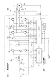
まず、各実施形態のMG制御装置が適用されるMG駆動システムの全体構成について図1を参照して説明する。図1には、一つのMGを備えるシステムを例示する。
MG駆動システム90は、充放電可能な二次電池である「電源」としてのバッテリ11の電圧をコンバータ20で所望のシステム電圧Vsysに昇圧し、昇圧された直流電力をインバータ30で三相交流電力に変換してMG80に供給するシステムである。
[System configuration]
First, the overall configuration of an MG drive system to which the MG control device of each embodiment is applied will be described with reference to FIG. FIG. 1 illustrates a system including one MG.
The
MG駆動システム90においてMG制御装置10は、主にコンバータ20、インバータ30、コンバータ制御部40及びインバータ制御部50を含む。コンバータ制御部40とインバータ制御部50とを合わせて、電力変換器制御部400と記す。なお、MG制御装置10は、二つ以上のMGを備えたMG駆動システムにも同様に適用可能である。
In the MG
MG80は、例えば永久磁石式同期型の三相交流モータである。本実施形態では、MG80は、ハイブリッド自動車の駆動輪を駆動するトルクを発生する電動機としての機能、及び、エンジンや駆動輪から伝達されるトルクを発電によってエネルギー回収する発電機としての機能を兼ね備える。 The MG 80 is, for example, a permanent magnet type synchronous three-phase AC motor. In the present embodiment, the MG 80 has a function as an electric motor that generates torque for driving the driving wheels of a hybrid vehicle, and a function as a generator that recovers energy by generating power from torque transmitted from the engine and driving wheels.
MG80の三相巻線81、82、83のうち二相の巻線に接続される電流経路には、相電流を検出する電流センサが設けられる。図1の例では、V相巻線82及びW相巻線83に接続される電流経路に、それぞれ相電流Iv、Iwを検出する電流センサ87、88が設けられており、残るU相の電流Iuをキルヒホッフの法則に基づいて推定している。他の実施形態では、どの二相の電流を検出してもよく、三相の電流を検出してもよい。或いは、一相の電流検出値に基づいて他の二相の電流を推定する技術を採用してもよい。
MG80の電気角θeは、例えばレゾルバ等の回転角センサ85により検出される。
A current sensor for detecting a phase current is provided in a current path connected to the two-phase winding among the three-
The electrical angle θe of the MG 80 is detected by a
以下の説明では、MG80の力行動作時におけるコンバータ20の昇圧動作について言及する。
コンバータ20は、フィルタコンデンサ21、リアクトル22、高電位側スイッチング素子23及び低電位側スイッチング素子24等を備える。
フィルタコンデンサ21は、コンバータ20の入力部に設けられ、バッテリ11からの電源ノイズを除去する。リアクトル22は、一端がバッテリ11に接続され、他端が高電位側スイッチング素子23と低電位側スイッチング素子24との接続点に接続される。リアクトル22は、電流の変化に伴って誘起電圧が発生し、電気エネルギーが蓄積される。
In the following description, the boosting operation of
The
The
高電位側スイッチング素子23及び低電位側スイッチング素子24は、インバータ30の母線とバッテリ11の低電位電極との間に直列に接続されている。高電位側スイッチング素子23及び低電位側スイッチング素子24は、コンバータ制御部40から指令されるゲート信号CU、CLにより相補的にオンオフする。
The high potential
高電位側スイッチング素子23がオフで低電位側スイッチング素子24がオンのとき、リアクトル22にリアクトル電流ILが流れることにより、エネルギーが蓄積される。
高電位側スイッチング素子23がオンで低電位側スイッチング素子24がオフのとき、リアクトル22に蓄積されたエネルギーが放出されることにより、バッテリ電圧Vbが昇圧されたシステム電圧Vsysが平滑コンデンサ25に充電される。
電圧センサ27はバッテリ電圧Vbを検出する。電流センサ28はリアクトル電流ILを検出する。
When the high-potential
When the high potential
The
インバータ30は、上下アームの6つのスイッチング素子31−36がブリッジ接続されている。詳しくは、スイッチング素子31、32、33は、それぞれU相、V相、W相の上アームのスイッチング素子であり、スイッチング素子34、35、36は、それぞれU相、V相、W相の下アームのスイッチング素子である。スイッチング素子31−36は、例えばIGBTで構成され、低電位側から高電位側へ向かう電流を許容する還流ダイオードが並列に接続されている。
In the
インバータ30は、インバータ制御部50からのゲート信号UU、UL、VU、VL、WU、WLに従ってスイッチング素子31−36が動作することで直流電力を三相交流電力に変換する。そして、インバータ制御部50が演算した電圧指令に応じた相電圧Vu、Vv、VwをMG80の各相巻線81、82、83に印加する。平滑コンデンサ25は、インバータ30に入力されるシステム電圧Vsysを平滑化する。
電圧センサ37はシステム電圧Vsysを検出する。電流センサ38はインバータ30の母線電流Imを検出する。なお、他の実施形態では、電流センサ38を備えず、後述する他の方法等により母線電流Imを算出してもよい。
The
The
コンバータ制御部40及びインバータ制御部50を含む電力変換器制御部400は、マイコン等により構成され、図示しないCPU、ROM、I/O、及び、これらの構成を接続するバスライン等を内部に備えている。マイコンは、予め記憶されたプログラムをCPUで実行することによるソフトウェア処理や、専用の電子回路によるハードウェア処理による制御を実行する。
The power
コンバータ制御部40は、電圧センサ27が検出したバッテリ電圧Vb、電流センサ28が検出したリアクトル電流IL、インバータ30に入力されるシステム電圧Vsys等の情報を取得する。そして、コンバータ制御部40は、MG80のトルク指令Trq*及び回転数ωに基づいて、システム電圧Vsysについての電圧指令値を算出する。
コンバータ制御部40による昇圧制御の詳細については後述する。
Details of the boost control by the
インバータ制御部50は、各センサが検出したシステム電圧Vsys、母線電流Im、二相の相電流Iv、Iw、電気角θeを取得する。また、インバータ制御部50は、微分器86により電気角θeが時間微分された電気角速度ω[deg/s]を取得する。電気角速度ωは、比例定数を乗じることにより回転数N[rpm]に換算されるため、本明細書では「電気角速度ωを換算した回転数」を省略して「回転数ω」という。なお、インバータ制御部50の内部に微分器86を有してもよい。
The
さらにインバータ制御部50は、上位制御回路からトルク指令Trq*が入力される。
インバータ制御部50は、これらの情報に基づいて、インバータ30を操作するゲート信号UU、UL、VU、VL、WU、WLを演算する。インバータ30は、ゲート信号UU、UL、VU、VL、WU、WLに従ってスイッチング素子31−36が動作することにより、バッテリ11から入力される直流電力を交流電力に変換しMG80に供給する。
Further, the
Based on such information, the
このような構成のMG制御装置10において、コンバータ20のリアクトル22と平滑コンデンサ25とにより構成されるLC共振回路では、式(1.1)で表される共振周波数frのLC共振が発生する。
fr=d/{2π√(LC)} ・・・(1.1)
ただし、
L :LC共振回路のインダクタンス
C :LC共振回路の容量
d :昇圧duty比
In the
fr = d / {2π√ (LC)} (1.1)
However,
L: LC resonance circuit inductance C: LC resonance circuit capacitance d: Boost duty ratio
また、インバータ30が出力する電圧波形が矩形波の場合等には、インバータ30の母線電流Imの振幅スペクトルに電気6次成分等の高次成分が重畳する。この電気6次成分の周波数fhは、式(1.2)で表される。
fh=pN/60 ・・・(1.2)
ただし、
p :MGの極対数
N :MGの回転数[rpm]
Further, when the voltage waveform output from the
fh = pN / 60 (1.2)
However,
p: Number of pole pairs of MG N: Number of rotations of MG [rpm]
式(1.1)、(1.2)より、電気6次周波数fhがLC共振周波数frに一致する回転数Nは、式(1.3)で求められる。
N=d×60/{2πp√(LC)} ・・・(1.3)
そのため、図2に示すように、時間に連れてMG80の回転数Nが上昇するとき、回転数NがLC共振領域に一致する期間にシステム電圧Vsysの電圧変動が発生する。
本実施形態は、このような電圧変動を抑制するための電力変換器制御部400の構成を特徴とする。以下、コンバータ制御部40及びインバータ制御部50の構成について詳しく説明する。
From equations (1.1) and (1.2), the rotational speed N at which the electrical sixth-order frequency fh matches the LC resonance frequency fr is obtained by equation (1.3).
N = d × 60 / {2πp√ (LC)} (1.3)
Therefore, as shown in FIG. 2, when the rotational speed N of the
The present embodiment is characterized by the configuration of the power
[インバータ制御部の構成、作用]
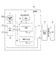
先にインバータ制御部50の構成及び作用について、図3〜図5を参照して説明する。
図3に示すように、インバータ制御部50は、dq変換部51、トルク推定部52、トルク減算器53、制御器54、電流指令演算部55、電流減算器56、制御器57、制御器58、電圧振幅/位相演算部59、変調器60、ゲート信号生成部79等を含む。このうち、制御器57と、制御器58及び電圧振幅/位相演算部59とは、フィードバック制御部(図中「FB制御部」)の構成に応じて選択的に設けられてもよい。
ここで、トルクフィードバック制御部540及び電流フィードバック制御部580は、インバータ30に指令する電圧ベクトルを演算する「電圧指令演算部」として機能する。以下の説明における「電圧ベクトル」は、基本的に「電圧指令ベクトル」を意味する。
[Configuration and operation of inverter control unit]
First, the configuration and operation of the
As shown in FIG. 3, the
Here, the torque
dq変換部51は、電気角θeに基づき、電流センサ87、88から取得した相電流をdq軸電流Id、Iqに変換し、電流減算器56にフィードバックする。
トルク推定部52は、dq軸電流Id、Iq、及び、MG80のモータ定数に基づき、式(2)を用いてトルク推定値Trq_estを算出する。なお、MG80にトルクセンサを備えたシステムでは、トルク推定部52を設けず、トルク検出値を取得してもよい。
Trq_est=p×{Iq×ψ+(Ld−Lq)×Id×Iq} ・・・(2)
ただし、
p :MGの極対数
ψ :逆起電圧定数
Ld、Lq:d軸インダクタンス、q軸インダクタンス
The
Trq_est = p × {Iq × ψ + (Ld−Lq) × Id × Iq} (2)
However,
p: number of pole pairs of MG ψ: counter electromotive voltage constant Ld, Lq: d-axis inductance, q-axis inductance
トルクフィードバック制御部540は、トルク減算器53及び制御器54を含む。
トルク減算器53は、トルク指令Trq*とトルク推定値Trq_estとのトルク偏差ΔTrqを算出する。制御器54は、トルク偏差ΔTrqを0に収束させるように、PI演算により電圧位相φを演算し、変調器60に出力する。こうして、トルクフィードバック制御部540は、MG80のトルクをフィードバック制御するための操作量として、電圧ベクトルの位相φを演算する。
The torque
Torque subtractor 53 calculates torque deviation ΔTrq between torque command Trq * and estimated torque value Trq_est. The
電流指令演算部55は、トルク指令Trq*に基づき、例えば電流当たり最大トルクが得られるように、マップや数式を用いてdq軸電流指令Id*、Iq*を演算する。
インバータ制御部50がトルクフィードバック制御部540を備える構成では、電流フィードバック制御部580は、電流減算器56及び制御器57を含む。
Based on the torque command Trq * , the current
In the configuration in which the
電流減算器56は、dq軸電流指令Id*、Iq*と、dq変換部51からフィードバックされるdq軸電流Id、Iqとの電流偏差ΔId、ΔIqを算出する。制御器57は、電流偏差ΔId、ΔIqを0に収束させるように、PI演算により電圧振幅Vrを演算し、変調器60に出力する。こうして、電流フィードバック制御部580は、MG80に流れる電流をフィードバック制御するための操作量として、電圧ベクトルの振幅Vrを演算する。
The
したがって、トルクフィードバック制御部540及び電流フィードバック制御部580が協働して「電圧指令演算部」を構成する場合、トルクフィードバック制御部540の制御器54が演算した電圧位相φ、及び、電流フィードバック制御部580の制御器57が演算した電圧振幅Vrが変調器60に出力される。
Therefore, when the torque
また、インバータ制御部50は、トルクフィードバック制御部540を備えず、電流フィードバック制御部580のみが「電圧指令演算部」を構成してもよい。この構成では、電流フィードバック制御部580は、電流減算器56、制御器58、及び電圧振幅/位相演算部59を含む。
制御器58は、電流偏差ΔId、ΔIqを0に収束させるように、PI演算によりdq軸電圧指令Vd*、Vq*を演算する。電圧振幅/位相演算部59は、dq軸電圧指令Vd*、Vq*を電圧振幅Vr及び電圧位相φに変換し、変調器60に出力する。なお、図3では電圧位相φをd軸基準で示しているが、q軸基準で電圧位相を定義してもよい。
Further, the
The
変調器60は、電圧振幅Vr及び電圧位相φに加え、システム電圧Vsys、電気角θe、回転数ω等の情報が入力される。変調器60は、これらの情報に基づき、インバータ30を操作するパルス電圧の出力波形としてパルスパターン又はPWM信号を出力する。
図4に示すように、変調器60は、変調率算出部61、方式切替部62、電圧波形特定部63を有する。電圧波形特定部63には、パルスパターン設定部64、記憶部65、PWM信号生成部66が含まれる。
The
As shown in FIG. 4, the
変調率算出部61は、電流フィードバック制御部580が出力した電圧振幅Vr、及びシステム電圧Vsysに基づいて、式(3)により変調率mを算出する。
m=2√(2/3)×(Vr/Vsys) ・・・(3)
方式切替部62は、変調率m等に基づいて、電圧波形特定部63による電圧波形の特定方式を切り替える。
The modulation
m = 2√ (2/3) × (Vr / Vsys) (3)
The
ここで、電圧波形の例について、図5(a)を参照する。
パルスパターンは、記憶部65に予め記憶された複数の電圧波形から、変調率m、回転数ω等に応じて、パルスパターン設定部64で選択される電圧波形である。
本明細書では、パルスパターンに、電気1周期に1パルスの矩形波を出力するパターンを含む。矩形波の変調率mは1.27で固定されるため、矩形波制御では電圧振幅Vrは一定であり、電圧位相φのみが操作される。三相交流モータを矩形波制御すると、相電圧及び相電流に含まれる電気周期6次、及び6の倍数の次数成分の割合が大きくなる。
Here, FIG. 5A is referred to for an example of a voltage waveform.
The pulse pattern is a voltage waveform selected by the pulse
In this specification, the pulse pattern includes a pattern that outputs a rectangular wave of one pulse in one electrical cycle. Since the modulation factor m of the rectangular wave is fixed at 1.27, in the rectangular wave control, the voltage amplitude Vr is constant and only the voltage phase φ is manipulated. When the three-phase AC motor is controlled by the rectangular wave, the ratio of the order component of the sixth and sixth multiples of the electrical cycle included in the phase voltage and phase current increases.
矩形波以外のパルスパターンは、変調率m、回転数ω等に応じて、電気1周期のパルス数、各パルスの位置及び幅により規定される。
PWM信号は、PWM信号生成部66において、電流フィードバック制御部580の出力に基づいて算出される相電圧と搬送波との比較により生成される。なお、詳しくは、相電圧が換算されたdutyと搬送波とが比較される。
電圧波形特定部63は、パルスパターン設定部64又はPWM信号生成部66の少なくとも一方を有する。
A pulse pattern other than a rectangular wave is defined by the number of pulses in one electrical cycle, the position and width of each pulse, according to the modulation factor m, the rotational speed ω, and the like.
The PWM signal is generated by the PWM
The voltage
方式切替部62は、変調率が1.27未満のとき、電圧波形の特定方式として、PWM信号、又は、矩形波以外のパルスパターンを選択する。PWM信号の場合、変調率が0〜1.15の範囲では正弦波PWMが用いられ、変調率が1.15〜1.27の範囲では過変調PWMが用いられる。
また、方式切替部62は、変調率が1.27のとき矩形波を選択する。これに応じて、インバータ制御部50は、電圧波形特定部63により特定する電圧波形が矩形波となったとき、電流フィードバック制御部580による制御を停止し、トルクフィードバック制御部540により電圧ベクトルを演算する。
When the modulation rate is less than 1.27, the
Further, the
こうして、電圧波形特定部63が特定したパルスパターン又はPWM信号の電圧波形がゲート信号生成部79に出力される。ゲート信号生成部79は、変調器60が出力した電圧波形に基づいて、ゲート信号UU、UL、VU、VL、WU、WLを生成し、インバータ30のスイッチング素子31−36に出力する。
In this way, the pulse pattern specified by the voltage
[コンバータ制御部の構成、作用]
次に、コンバータ制御部40の構成及び作用について、図6〜図12を参照して説明する。
図6に示すように、コンバータ制御部40は、電圧指令基準値算出部41、昇圧/非昇圧状態判定部42、電圧指令値変更部43、昇圧制御部44等を含む。
[Configuration and operation of converter control unit]
Next, the configuration and operation of
As shown in FIG. 6,
電圧指令基準値算出部41は、MG80のトルク指令Trq*及び回転数ω(又はN)に基づいてシステム要求電圧である電圧指令基準値Vsys*を算出する。
昇圧/非昇圧状態判定部42は、基本例である第1実施形態では、電源電圧Vb及び電圧指令基準値Vsys*を取得する。その他、昇圧/非昇圧状態判定の構成に応じて、システム電圧Vsysの検出値や、インバータ制御部50の変調器60が特定した電圧波形や変調率mの情報を取得する。
Voltage command reference
In the first embodiment, which is a basic example, the boosting / non-boosting
昇圧/非昇圧状態判定部42は、これらの情報に基づき、次回の制御で要求されるコンバータ20の状態が昇圧状態であるか非昇圧状態であるかを判定する。昇圧/非昇圧状態判定構成についての詳細は後述する。
ここで本実施形態では、コンバータ20の「昇圧状態」とは、例えば図8に参照されるような「高電位側スイッチング素子23のオン状態とオフ状態とが継続的に交替している状態」と定義する。これに対し、「非昇圧状態」は、「高電位側スイッチング素子23がオン状態を継続している状態」と定義される。
Based on these pieces of information, boost / non-boosting
Here, in the present embodiment, the “boosting state” of the
電圧指令値変更部43は、昇圧/非昇圧状態判定部42による判定結果、及び、振幅スペクトル抽出部71からの特定周波数の振幅スペクトルの情報に基づき、所定の条件が成立したとき、電圧指令基準値算出部41が演算した電圧指令基準値Vsys*を変更し、変更後電圧指令値Vsys**を昇圧制御部44に出力する。ここで、特定周波数とは、母線電流Imが流れる回路のLC共振周波数に相当する周波数である。
さらに、図6に破線で示すように、電圧指令値変更部43は、インバータ制御部50の変調器60が特定した電圧波形や変調率mの情報を取得してもよい。
Based on the determination result by the boost / non-boost
Furthermore, as indicated by a broken line in FIG. 6, the voltage command
詳しくは、電圧指令値変更部43は、振幅スペクトル抽出部71からの情報により母線電流Imの特定周波数の振幅スペクトルが判定閾値以上であり、且つ、昇圧/非昇圧状態判定部42による判定結果が非昇圧状態であるとき、昇圧状態とする処理を行う。
一方、所定の条件が成立しないとき、電圧指令値変更部43は、入力された電圧指令基準値Vsys*をそのまま変更後電圧指令値Vsys**として出力する。
特に三相交流モータであるMG80を矩形波制御する場合、電圧指令値変更部43は、母線電流Imの電気6次等の周波数がLC共振周波数と一致するMG80の回転数ωでコンバータ20を昇圧状態とするように電圧指令基準値Vsys*を変更する。
Specifically, the voltage command
On the other hand, when the predetermined condition is not satisfied, the voltage command
In particular, when the MG80, which is a three-phase AC motor, is subjected to rectangular wave control, the voltage command
「昇圧状態とする」とは、現在が非昇圧状態の場合は、次回の制御で昇圧状態に移行することを意味する。また、現在が昇圧状態の場合は、次回の制御で非昇圧状態に移行することを禁止し昇圧状態を維持することを意味する。この両方の場合を含めて、「昇圧状態とする処理」を「昇圧状態移行処理」という。
一方、「非昇圧状態に移行する」とは、現在の昇圧状態から、次回の制御で非昇圧状態に移行する場合と、現在の非昇圧状態を維持する場合の両方を含むものとする。
“To be in a boosted state” means that if the current state is a non-boosted state, transition to the boosted state is performed in the next control. Further, when the current state is the boosted state, it means that the transition to the non-boosted state is prohibited in the next control and the boosted state is maintained. Including both cases, the “process for setting the boosted state” is referred to as “boosted state transition process”.
On the other hand, “transition to the non-boosting state” includes both the case of shifting from the current boosting state to the non-boosting state in the next control and the case of maintaining the current non-boosting state.
昇圧制御部44は、変更後電圧指令値Vsys**、電源電圧Vb、及び、電圧センサ37が検出したシステム電圧Vsysを取得する。さらに、本実施形態の昇圧制御部44は、電流センサ27が検出したリアクトル電流ILを取得する。なお、電圧指令値変更部43による指令値変更を要しない場合、変更後電圧指令値Vsys**として、電圧指令基準値Vsys*がそのまま取得される。
昇圧制御部44は、これらの情報に基づいて、高電位側スイッチング素子23及び低電位側スイッチング素子24を駆動するゲート信号CU、CLを生成する。このとき、昇圧制御部44は、高電位側スイッチング素子23及び低電位側スイッチング素子24が同時にオフするデッドタイムDTを設定する。デッドタイムDTの情報は、電圧指令値変更部43に通知される。
The
The
変更後電圧指令値Vsys**がバッテリ電圧Vbよりも高い場合、バッテリ電圧Vbの昇圧が要求される昇圧状態となる。このとき、コンバータ制御部40は、バッテリ電圧Vbを変更後電圧指令値Vsys**にまで昇圧させるようにゲート信号CU、CLを生成し、高電位側スイッチング素子23及び低電位側スイッチング素子24を交互にオン動作させる。
一方、変更後電圧指令値Vsys**がバッテリ電圧Vb以下の場合、昇圧が要求されない非昇圧状態となる。このとき、コンバータ制御部40は、バッテリ電圧Vbを昇圧せずインバータ30に出力する。非昇圧状態では、高電位側スイッチング素子23がオンで低電位側スイッチング素子24がオフの状態が継続する。
When the post-change voltage command value Vsys ** is higher than the battery voltage Vb, a boosted state is required in which boosting of the battery voltage Vb is required. At this time, the
On the other hand, when the post-change voltage command value Vsys ** is equal to or lower than the battery voltage Vb, a non-boosted state where boosting is not required is entered. At this time,
ここで、コンバータ20の昇圧制御に関し、例えば特開2014−158328号公報には、リアクトル電流ILの検出値に基づいて昇圧電圧を制御する電流モード制御の技術が開示されている。本実施形態の昇圧制御部44は、電流モード制御方式を採用することにより、昇圧時、インバータ30に出力するシステム電圧Vsysを安定化させ、電圧変動を抑制することができる。
本実施形態では、この点に着目し、インバータ30の母線電流Imが有する振幅スペクトルの特定周波数がLC共振周波数と一致し、特定周波数の振幅スペクトルが判定閾値以上であるとき、コンバータ20を昇圧状態とするように制御する。これにより、電圧変動を適切に抑制することができる。以上がコンバータ制御部40の構成の概要である。
Here, regarding boost control of the
In the present embodiment, paying attention to this point, when the specific frequency of the amplitude spectrum of the bus current Im of the
続いて、コンバータ制御部40の各部の詳細について補足する。まず、第1実施形態として、電圧指令基準値Vsys*の変更に関する基本的な実施例を図7に示す。
時刻to以前の非昇圧状態では、電圧指令基準値Vsys*は電源電圧Vbに等しい。そして、時刻toに、非昇圧状態から昇圧状態に移行する必要があると判断すると、電圧指令値変更部43は、電圧指令基準値Vsys*を少なくとも電源電圧Vbより大きい値の変更後電圧指令値Vsys**に変更する。「非昇圧状態から昇圧状態に移行する」ということは、「非昇圧状態の維持を禁止する」と言い換えてもよい。
電源電圧Vbに対する変更後電圧指令値Vsys**の最小増加分ΔVminは、制御の応答特性や制御誤差等に応じて適宜設定してよい。例えば、次に説明するデッドタイムDTに基づいて最小増加分ΔVminを設定してもよい。
Then, it supplements about the detail of each part of the
In the non-boosted state before time to, voltage command reference value Vsys * is equal to power supply voltage Vb. When determining that it is necessary to shift from the non-boosted state to the boosted state at time to, the voltage command
The minimum increment ΔVmin of the post-change voltage command value Vsys ** with respect to the power supply voltage Vb may be set as appropriate according to control response characteristics, control error, and the like. For example, the minimum increase ΔVmin may be set based on a dead time DT described below.
電圧指令基準値算出部41又は電圧指令値変更部43が非昇圧状態を禁止するための具体的手段として、以下の考え方が挙げられる。ここでは、電圧指令値変更部43が変更後電圧指令値Vsys**を設定する場合に限らず、電圧指令基準値算出部41が最初から好ましい電圧指令基準値Vsys*を設定する場合を含めて記載する。
[1]上述通り、電圧指令値(Vsys*又はVsys**)を電源電圧Vbより大きい値に変更する。
As specific means for the voltage command reference
[1] As described above, the voltage command value (Vsys * or Vsys ** ) is changed to a value larger than the power supply voltage Vb.
[2]電圧指令値(Vsys*又はVsys**)を、少なくとも「デッドタイムDTによる電圧低下分を補償するように昇圧する電圧指令値」以上に設定する。例えば、LC共振領域での電圧指令値の設定において、「デッドタイム補償分を昇圧する電圧指令値」と、「システム損失低減から要求される電圧指令値」との大きい方の値を選択する。 [2] The voltage command value (Vsys * or Vsys ** ) is set to at least “voltage command value to be boosted so as to compensate for the voltage drop due to the dead time DT”. For example, in setting the voltage command value in the LC resonance region, a larger value of “voltage command value for boosting dead time compensation” and “voltage command value required for reducing system loss” is selected.
ここで、図8に示すように、デッドタイムDTは、スイッチング周期Tsw中の高電位側スイッチング素子23(図中「上アーム」)のオン期間TUと低電位側スイッチング素子24(図中「下アーム」)のオン期間TLとの間に設定される。上アーム指令値の立ち下がりから下アーム指令値の立ち下がりまでと、下アーム指令値の立ち下がりから上アーム指令値の立ち上がりまでのデッドタイムDTが等しい場合、デッドタイム比率RDTは、式(4)で算出される。
RDT=2DT/Tsw ・・・(4)
そこで、電圧指令値変更部43は、少なくともデッドタイムDTによる電圧低下補償分を昇圧するように、電圧指令値を設定することが好ましい。
Here, as shown in FIG. 8, the dead time DT corresponds to the ON period TU of the high potential side switching element 23 (“upper arm” in the figure) and the low potential side switching element 24 (“lower” in the figure) during the switching cycle Tsw. It is set between the ON period TL of the arm “)”. When the dead time DT from the fall of the upper arm command value to the fall of the lower arm command value is equal to the dead time DT from the fall of the lower arm command value to the rise of the upper arm command value, the dead time ratio R DT It is calculated in 4).
R DT = 2DT / Tsw (4)
Therefore, it is preferable that the voltage command
[3]電圧指令値(Vsys*又はVsys**)を、少なくとも「非昇圧状態に移行しない最低の電圧値」以上に設定する。この考え方は、非昇圧状態への移行を電圧で判断するシステムでの適用を想定する。例えば、LC共振領域での電圧指令値の設定において、「非昇圧状態に移行しない最低の電圧値」と、「システム損失低減から要求される電圧指令値」との大きい方の値を選択する。
なお、[2]又は[3]における「システム損失低減から要求される電圧指令値」は、例えば特許第5618948号公報に開示された、矩形波制御での電流指令ベクトルを最適電流進角ラインに追従させる技術に基づいて設定可能である。
[3] The voltage command value (Vsys * or Vsys ** ) is set to at least “the lowest voltage value that does not shift to the non-boosted state” or more. This concept assumes application in a system that determines the transition to the non-boosted state by voltage. For example, in the setting of the voltage command value in the LC resonance region, the larger value of “the lowest voltage value that does not shift to the non-boosted state” and “the voltage command value required from the system loss reduction” is selected.
The “voltage command value required from system loss reduction” in [2] or [3] is the current command vector in rectangular wave control disclosed in, for example, Japanese Patent No. 5618948. It can be set based on the technology to be followed.
次に、昇圧/非昇圧状態判定部42による昇圧/非昇圧状態判定について、図7に示したように、電源電圧Vbと電圧指令基準値Vsys*との比較により昇圧/非昇圧状態を判定する構成を第1実施形態とする。また、それ以外の方法で昇圧/非昇圧状態を判定する構成を第2、第3実施形態として、図9を参照して説明する。
図6において昇圧/非昇圧状態判定部42が取得する情報として、一点鎖線で示すシステム電圧Vsysは、第2実施形態で用いられる。
Next, regarding the boost / non-boost state determination by the boost / non-boost
As information acquired by the boosting / non-boosting
図9(a)に示す第2実施形態では、システム電圧Vsysについての閾値Vsys_thが設定される。昇圧/非昇圧状態判定部42は、電圧センサ37が検出したシステム電圧Vsysの検出値を取得する。図9(a)において、時刻tx以前は、システム電圧Vsysが閾値Vsys_thより大きい昇圧状態である。その後、時刻txにシステム電圧Vsysが閾値Vsys_thを下回ると、昇圧/非昇圧状態判定部42は、昇圧状態から非昇圧状態への移行要求が生じたと判定し、電圧指令値変更部43に通知する。
このとき、特定周波数の振幅スペクトルが判定閾値以上である場合、電圧指令値変更部43は、電圧指令基準値Vsys*をシステム電圧閾値Vsys_thより大きい値に変更する。
In the second embodiment shown in FIG. 9A, a threshold value Vsys_th for the system voltage Vsys is set. The step-up / non-step-up
At this time, when the amplitude spectrum of the specific frequency is greater than or equal to the determination threshold, the voltage command
図9(b)に示す第3実施形態では、電圧指令基準値Vsys*についての閾値Vsys*_thが設定される。昇圧/非昇圧状態判定部42は、電圧指令基準値算出部41が算出した電圧指令基準値Vsys*を取得する。図9(b)において、時刻tx以前は、電圧指令基準値Vsys*が閾値Vsys*_thより大きい昇圧状態である。その後、時刻txに電圧指令基準値Vsys*が閾値Vsys*_thを下回ると、昇圧/非昇圧状態判定部42は、昇圧状態から非昇圧状態への移行要求が生じたと判定し、電圧指令値変更部43に通知する。
このとき、特定周波数の振幅スペクトルが判定閾値以上である場合、電圧指令値変更部43は、電圧指令基準値Vsys*を基準値閾値Vsys*_thより大きい値に変更する。
In the third embodiment shown in FIG. 9 (b), the threshold Vsys * - th of the voltage command reference value Vsys * is set. The step-up / non-step-up
At this time, when the amplitude spectrum of the specific frequency is greater than or equal to the determination threshold, the voltage command
加えて、第2、第3実施形態におけるシステム電圧閾値Vsys_thや基準値閾値Vsys*_thは、上述の「デッドタイム補償分を昇圧する電圧指令値」の最小値以上の値に設定されるようにすることが好ましい。これにより、デッドタイムを要因として実際に非昇圧状態となることを防止することができる。 In addition, the system voltage threshold value Vsys_th and the reference value threshold value Vsys * _th in the second and third embodiments are set to a value equal to or greater than the minimum value of the above-described “voltage command value for boosting the dead time compensation”. It is preferable to do. As a result, the actual non-boosted state can be prevented due to the dead time.
次に振幅スペクトル抽出部71は、インバータ30の母線電流Imを取得し、母線電流Imの特定周波数の振幅スペクトルを、高速フーリエ変換(図中「FFT」)やマップ等により抽出する。
上述の通り、インバータ30の母線電流Imが有する振幅スペクトルの分布は、電圧波形特定部63が特定する出力電圧波形によって異なる。図5(b)を参照すると、例えばトルクフィードバック制御により矩形波を出力する場合、矩形波以外のパルスパターンやPWM信号を出力する場合に比べ、電気周期6次等の振幅スペクトルが大きくなる。
Next, the amplitude
As described above, the distribution of the amplitude spectrum of the bus current Im of the
この場合、回転数ωにより換算した電気周期6次等の周波数を「特定周波数」とすると、コンバータ20のLC共振周波数に特定周波数が一致したとき、共振による電圧変動が増大するおそれがある。
In this case, assuming that the frequency of the electrical cycle 6th order or the like converted by the rotational speed ω is “specific frequency”, voltage fluctuation due to resonance may increase when the specific frequency matches the LC resonance frequency of the
ここで、母線電流Imの振幅スペクトルは、以下の方法等により算出可能である。
[1]母線電流Imを逐次、高速フーリエ変換することにより算出する。母線電流Imは電流センサ38で検出する以外に、相電流検出値又は指令値と相電圧との積をインバータ電圧で除することにより算出してもよい。
[2]図10に示すように、予めスペクトル解析した母線電流Imの振幅スペクトルを力率、変調率毎に記憶しておき、電圧波形、力率、変調率m、回転数ω、搬送波周波数に応じて適当なスペクトルを選択し、相電流振幅で振幅を補正する。
Here, the amplitude spectrum of the bus current Im can be calculated by the following method or the like.
[1] The bus current Im is calculated by sequentially performing a fast Fourier transform. The bus current Im may be calculated by dividing the product of the phase current detection value or command value and the phase voltage by the inverter voltage in addition to the detection by the
[2] As shown in FIG. 10, the amplitude spectrum of the bus current Im subjected to spectrum analysis in advance is stored for each power factor and modulation factor, and the voltage waveform, power factor, modulation factor m, rotation speed ω, and carrier frequency are stored. Accordingly, an appropriate spectrum is selected, and the amplitude is corrected by the phase current amplitude.
また、特定周波数の振幅スペクトルについての判定閾値は、次のように設定することが好ましい。
[1]システム電圧Vsysの変動が所定の制限値以下に抑制されるように設定する。
例えば図11に示すように、耐圧上限値Vresと最大システム電圧Vsysとの差分から、スイッチング素子31−36のスイッチング動作に伴う電圧サージ量、及び、電圧センサ37の検出誤差を差し引いた値を、電圧変動制限値とする。
[2]矩形波の電気6次成分の振幅スペクトルを基準値として、例えば、基準値自体、又は基準値の50%相当値等を判定閾値としてもよい。
Moreover, it is preferable to set the determination threshold for the amplitude spectrum of the specific frequency as follows.
[1] It is set so that the fluctuation of the system voltage Vsys is suppressed below a predetermined limit value.
For example, as shown in FIG. 11, a value obtained by subtracting the voltage surge amount accompanying the switching operation of the switching elements 31-36 and the detection error of the
[2] The amplitude spectrum of the electrical sixth-order component of the rectangular wave may be used as the reference value, for example, the reference value itself or a value equivalent to 50% of the reference value may be used as the determination threshold value.
次に、昇圧状態移行処理のフローチャートを図12に示す。以下のフローチャートの説明で、記号「S」はステップを意味する。また、フローチャートの各ステップの制御主体は、コンバータ制御部40又はインバータ制御部50である。
S1では、電流フィードバック制御部580で電圧振幅Vrを演算し、トルクフィードバック制御部540で電圧位相φを演算することにより電圧ベクトルを演算する。
Next, a flowchart of the boost state transition process is shown in FIG. In the description of the flowchart below, the symbol “S” means a step. Further, the control subject of each step in the flowchart is the
In S1, the voltage vector V is calculated by calculating the voltage amplitude Vr by the current
S2では、回転数ωを取得する。
S3では、電圧波形特定部63でインバータの出力電圧波形を特定する。
S4では、振幅スペクトル抽出部71は、インバータ母線電流Imを取得する。
In S2, the rotational speed ω is acquired.
In S3, the voltage
In S4, the amplitude
S5では、振幅スペクトル抽出部71が抽出した特定周波数の振幅スペクトルが判定閾値以上であるか判断する。S5にてNOの場合、S8に移行する。
S5でYESの場合、S6では、システム要求に基づく電圧指令基準値Vsys*が電源電圧Vb以下であるか判断する。電圧指令基準値Vsys*が電源電圧Vb以下であり、S6にてYESの場合、現在の非昇圧状態を維持する要求、又は、現在の昇圧状態から非昇圧状態への移行要求があると判断される。この場合、S7に移行する。
一方、電圧指令基準値Vsys*が電源電圧Vbを超えており、S6にてNOの場合、現在の昇圧状態を維持する要求、又は、現在の非昇圧状態から昇圧状態への移行要求があると判断される。この場合、S8に移行する。
In S5, it is determined whether the amplitude spectrum of the specific frequency extracted by the amplitude
If YES in S5, it is determined in S6 whether the voltage command reference value Vsys * based on the system request is equal to or lower than the power supply voltage Vb. If voltage command reference value Vsys * is equal to or lower than power supply voltage Vb and YES in S6, it is determined that there is a request to maintain the current non-boosted state or a request to transition from the current boosted state to the non-boosted state. The In this case, the process proceeds to S7.
On the other hand, when voltage command reference value Vsys * exceeds power supply voltage Vb and NO in S6, there is a request to maintain the current boosted state or a request to shift from the current non-boosted state to the boosted state. To be judged. In this case, the process proceeds to S8.
S7では、昇圧制御により、LC共振による電圧変動を抑制するため、変更後電圧指令値Vsys**を電源電圧Vbより大きい値で再設定し、コンバータ20を昇圧状態とする。
一方、S8では、LC共振による電圧変動を抑制する必要性が低いため、システム要求に基づく電圧指令基準値Vsys*を、そのまま変更後電圧指令値Vsys**として出力する。
以上で、昇圧状態移行処理のルーチンを終了する。
In S7, in order to suppress voltage fluctuation due to LC resonance by boost control, the changed voltage command value Vsys ** is reset to a value larger than the power supply voltage Vb, and the
On the other hand, in S8, since it is less necessary to suppress voltage fluctuation due to LC resonance, the voltage command reference value Vsys * based on the system request is output as it is as the changed voltage command value Vsys ** .
This is the end of the boost state transition processing routine.
以上のように、本実施形態のMG制御装置10は、LC共振周波数に相当する母線電流Imの特定周波数の振幅スペクトルが判定閾値以上であり、且つ、非昇圧状態であるとき、コンバータ20を昇圧状態とするように電圧指令基準値Vsys*を変更する。
これにより、本実施形態のMG制御装置10は、LC共振領域において常に正弦波制御方式を用いる従来技術のようにシステム損失を低下させることなく、システム電圧Vsysの電圧変動を適切に抑制することができる。
As described above, the
Thereby, the
(その他の実施形態)
(a)上記実施形態では、コンバータ制御部40の昇圧制御部44は、電流センサ28が検出したリアクトル電流ILに基づく電流モード制御方式によりシステム電圧Vsysを安定化させている。他の実施形態では、昇圧制御部44は、電流モード制御以外の方式でシステム電圧Vsysを安定させるようにしてもよい。いずれの昇圧制御方式にせよ、昇圧状態にすることで、インバータ出力電圧波形の電気6次等の周波数とLC共振周波数とが一致する場合でも電圧変動を抑制可能であれば、本発明に適用可能である。
(Other embodiments)
(A) In the above embodiment, the
(b)上記実施形態では、「高電位側スイッチング素子23のオン状態とオフ状態とが継続的に交替している状態」を「昇圧状態」と定義している。この他、リアクトル電流ILの増加、減少の状態等に基づいて、昇圧状態を定義してもよい。
(B) In the above embodiment, “a state in which the ON state and the OFF state of the high potential
(c)三相交流モータの制御装置を想定した上記実施形態では、LC共振周波数と一致したとき電圧変動に与える影響が大きいと考えられる次数成分として、特に電気6次成分や12次、18次等の成分に注目している。中でも矩形波制御では、母線電流Imの振幅スペクトルに電気6次等の成分が大きく現れるため、本発明による昇圧状態移行処理が有効である。 (C) In the above-described embodiment assuming a control device for a three-phase AC motor, the order components that are considered to have a large effect on voltage fluctuation when matched with the LC resonance frequency, in particular, the electrical sixth-order component, the 12th-order, and the 18th-order We pay attention to ingredients such as. In particular, in the rectangular wave control, a component such as an electric sixth order appears greatly in the amplitude spectrum of the bus current Im, so that the boost state transition processing according to the present invention is effective.
ただし、矩形波以外のパルスパターンでも、電気6次等の成分の割合が大きいものがある。そこで、例えばパルスパターンとモータ電流振幅、力率のマップ等を用いて、パルスパターンの電圧波形とモータ電流とから母線電流Imの電気6次等の振幅を算出し、電気6次等の振幅が所定値以上であることを指標として、処理対象とする電圧波形を選択してもよい。 However, some pulse patterns other than the rectangular wave have a large ratio of components such as the electrical sixth order. Therefore, for example, using the pulse pattern, motor current amplitude, power factor map, etc., the electric sixth-order amplitude of the bus current Im is calculated from the voltage waveform of the pulse pattern and the motor current. A voltage waveform to be processed may be selected using an index that is equal to or greater than a predetermined value.
(d)また、本発明が適用されるシステムにおいて駆動される多相交流モータの相の数は、四相以上であってもよい。また、永久磁石式同期型モータに限らず、誘導電動機やその他の同期モータであってもよい。このような電動機の特性等に応じて、母線電流Imの振幅スペクトルに大きく現れる次数成分は、随時異なる。 (D) Moreover, the number of phases of the multiphase AC motor driven in the system to which the present invention is applied may be four or more. Moreover, not only a permanent magnet type synchronous motor but an induction motor or other synchronous motors may be used. Depending on the characteristics of such an electric motor, etc., the order component that appears greatly in the amplitude spectrum of the bus current Im varies from time to time.
(e)インバータ制御部は、フィードバック制御に限らず、フィードフォワード制御により電圧ベクトルを演算してもよい。
(f)本発明による交流電動機の制御装置は、ハイブリッド自動車や電気自動車のMG駆動システムに限らず、一般機械用等、どのような用途の交流電動機の駆動システムに適用されてもよい。
以上、本発明は、上記実施形態になんら限定されるものではなく、発明の趣旨を逸脱しない範囲において種々の形態で実施可能である。
(E) The inverter control unit is not limited to feedback control, and may calculate a voltage vector by feedforward control.
(F) The control apparatus for an AC motor according to the present invention is not limited to an MG drive system for a hybrid vehicle or an electric vehicle, but may be applied to an AC motor drive system for any application, such as for general machinery.
As mentioned above, this invention is not limited to the said embodiment at all, In the range which does not deviate from the meaning of invention, it can implement with a various form.
10・・・MG制御装置(交流電動機の制御装置)、 11・・・バッテリ(電源)、
20・・・コンバータ、
23・・・高電位側スイッチング素子、 24・・・低電位側スイッチング素子、
30・・・インバータ、 31−36・・・スイッチング素子、
40・・・コンバータ制御部、 41・・・電圧指令基準値算出部、
42・・・昇圧/非昇圧状態判定部、 43・・・電圧指令値変更部、
50・・・インバータ制御部、
540・・・トルクフィードバック制御部(電圧指令演算部)、
580・・・電流フィードバック制御部(電圧指令演算部)、
63・・・電圧波形特定部、
64・・・パルスパターン設定部、 66・・・PWM信号生成部、
71・・・振幅スペクトル抽出部、
80・・・MG(交流電動機)。
10 ... MG control device (control device for AC motor), 11 ... Battery (power supply),
20 ... Converter,
23 ... high potential side switching element, 24 ... low potential side switching element,
30 ... Inverter, 31-36 ... Switching element,
40 ... converter control unit, 41 ... voltage command reference value calculation unit,
42: Boost / non-boosted state determination unit, 43 ... Voltage command value change unit,
50: Inverter control unit,
540 ... Torque feedback control unit (voltage command calculation unit),
580 ... Current feedback control unit (voltage command calculation unit),
63 ... Voltage waveform specifying part,
64 ... pulse pattern setting unit, 66 ... PWM signal generation unit,
71 ... Amplitude spectrum extraction unit,
80: MG (AC motor).
Claims (10)
前記コンバータから出力された前記システム電圧の直流電力を複数のスイッチング素子(31−36)の動作により交流電力に変換し交流電動機(80)に供給するインバータ(30)と、
前記システム電圧についての電圧指令値を算出し、前記コンバータの動作を制御するコンバータ制御部(40)と、
前記インバータに指令する電圧ベクトルを演算する電圧指令演算部(540、580)、及び、前記電圧ベクトルに基づき前記インバータを操作する電圧波形を特定する電圧波形特定部(63)を有するインバータ制御部(50)と、
を備え、
前記コンバータ制御部は、
前記交流電動機のトルク及び回転数に基づいて前記電圧指令値の基準値である電圧指令基準値(Vsys*)を算出する電圧指令基準値算出部(41)と、
次回の制御で前記コンバータに要求される状態が、前記電源電圧を昇圧して出力する昇圧状態、又は、前記電源電圧を昇圧せず出力する非昇圧状態のいずれであるかを判定する昇圧/非昇圧状態判定部(42)と、
前記昇圧/非昇圧状態判定部による判定結果が非昇圧状態であるとき、前記コンバータのLC共振周波数に相当する特定周波数の振幅スペクトルが判定閾値以上であることを、少なくとも前記電圧波形、前記交流電動機の回転数、前記インバータに流れる電流の振幅、前記インバータの搬送波周波数、力率、変調率のうち一つ以上に基づいて判定し、前記コンバータを昇圧状態とするように前記電圧指令基準値を変更する電圧指令値変更部(43)と、
を有する交流電動機の制御装置。 Converter capable of boosting the power supply voltage (Vb) supplied from the DC power supply (11) to a desired system voltage (Vsys) by the operation of the high potential side switching element (23) and the low potential side switching element (24) ( 20)
An inverter (30) that converts the DC power of the system voltage output from the converter into AC power by operation of a plurality of switching elements (31-36) and supplies the AC power to the AC motor (80);
A converter controller (40) for calculating a voltage command value for the system voltage and controlling the operation of the converter;
Inverter control unit having a voltage command calculation unit (540, 580) for calculating a voltage vector commanded to the inverter, and a voltage waveform specifying unit (63) for specifying a voltage waveform for operating the inverter based on the voltage vector ( 50) ,
With
The converter controller is
A voltage command reference value calculation unit (41) that calculates a voltage command reference value (Vsys * ), which is a reference value of the voltage command value, based on the torque and rotation speed of the AC motor;
Boost / non-determining whether a state required for the converter in the next control is a boost state in which the power supply voltage is boosted and output or a non-boost state in which the power supply voltage is not boosted and output A step-up state determination unit (42);
When the judgment result by the previous SL-up / non-boosting state determination unit is a non-boosting state, the amplitude spectrum of a specific frequency corresponding to the LC resonant frequency of the converter is equal to or greater than the determination threshold value, at least the voltage waveform, the AC Judgment is made based on one or more of the rotation speed of the motor, the amplitude of the current flowing through the inverter, the carrier frequency of the inverter, the power factor, and the modulation factor, and the voltage command reference value is set so that the converter is in a boosted state. A voltage command value changing unit (43) to be changed;
A control apparatus for an AC electric motor.
前記電圧指令値変更部は、前記特定周波数の振幅スペクトルが前記判定閾値以上であると判定した場合、前記電圧指令基準値を前記システム電圧閾値より大きい値に変更する請求項1または2に記載の交流電動機の制御装置。 The boosting / non-boosting state determination unit determines that a request for transition from the boosting state to the non-boosting state has occurred when the detected value of the system voltage falls below a system voltage threshold (Vsys_th),
3. The voltage command value change unit according to claim 1, wherein the voltage command value changing unit changes the voltage command reference value to a value larger than the system voltage threshold value when it is determined that an amplitude spectrum of the specific frequency is equal to or greater than the determination threshold value. AC motor control device.
前記電圧指令値変更部は、前記特定周波数の振幅スペクトルが前記判定閾値以上であると判定した場合、前記電圧指令基準値を前記基準値閾値より大きい値に変更する請求項1または2に記載の交流電動機の制御装置。 The step-up / non-step-up state determination unit determines that a request for transition from the step-up state to the non-step-up state has occurred when the voltage command reference value falls below a reference value threshold (Vsys * _th),
3. The voltage command value change unit according to claim 1, wherein the voltage command value changing unit changes the voltage command reference value to a value larger than the reference value threshold when it is determined that an amplitude spectrum of the specific frequency is equal to or greater than the determination threshold. AC motor control device.
前記電圧指令値変更部は、
前記電圧指令基準値を、前記デッドタイムによる電圧低下分を補償するように昇圧する電圧指令値以上に変更する請求項1〜4のいずれか一項に記載の交流電動機の制御装置。 In the converter, a dead time is set between an on period of the high potential side switching element and an on period of the low potential side switching element,
The voltage command value changing unit is
The control apparatus for an AC motor according to any one of claims 1 to 4, wherein the voltage command reference value is changed to a voltage command value or more that is boosted so as to compensate for a voltage drop due to the dead time.
前記交流電動機を流れる電流をフィードバック制御するための操作量として前記電圧ベクトルを演算する電流フィードバック制御部(580)を含み、
前記電圧波形特定部は、
前記電流フィードバック制御部が出力した電圧振幅及びシステム電圧から算出される変調率と前記交流電動機の回転数とに基づいて、予め記憶された複数のパルスパターンからいずれかのパルスパターンを選択するパルスパターン設定部(64)、又は、前記電流フィードバック制御部の出力に基づいて算出される相電圧と搬送波との比較によりPWM信号を生成するPWM信号生成部(66)の少なくとも一方を有する請求項1〜5のいずれか一項に記載の交流電動機の制御装置。 The voltage command calculator is
A current feedback control unit (580) that calculates the voltage vector as an operation amount for feedback control of the current flowing through the AC motor;
The voltage waveform specifying unit includes:
A pulse pattern for selecting any one of a plurality of pulse patterns stored in advance based on a modulation factor calculated from the voltage amplitude and system voltage output from the current feedback control unit and the rotational speed of the AC motor The setting unit (64) or at least one of a PWM signal generation unit (66) that generates a PWM signal by comparing a phase voltage calculated based on an output of the current feedback control unit and a carrier wave. The control apparatus for an AC motor according to claim 5.
前記交流電動機のトルクをフィードバック制御するための操作量として前記電圧ベクトルの位相を演算するトルクフィードバック制御部(540)をさらに含み、
前記電圧波形特定部は、前記パルスパターン設定部(64)を有し、
前記トルクフィードバック制御部により電圧ベクトルを演算する場合、前記パルスパターン設定部は、電気1周期に1パルスの矩形波を出力するパターンを選択する請求項6に記載の交流電動機の制御装置。 The voltage command calculator is
A torque feedback control unit (540) that calculates the phase of the voltage vector as an operation amount for feedback control of the torque of the AC motor;
The voltage waveform specifying unit includes the pulse pattern setting unit (64),
The control apparatus for an AC motor according to claim 6, wherein, when the voltage vector is calculated by the torque feedback control unit, the pulse pattern setting unit selects a pattern that outputs a rectangular wave of one pulse in one electrical cycle.
前記電圧指令演算部は、前記電流フィードバック制御部による制御を停止し、前記トルクフィードバック制御部により前記電圧ベクトルを演算する請求項7に記載の交流電動機の制御装置。 When the voltage waveform specified by the voltage waveform specifying unit is a rectangular wave,
The control apparatus for an AC motor according to claim 7, wherein the voltage command calculation unit stops control by the current feedback control unit and calculates the voltage vector by the torque feedback control unit.
前記電圧波形特定部が特定する電圧波形が矩形波となったとき、
前記電圧指令値変更部は、
前記インバータの母線電流(Im)の電気6次周波数が前記コンバータのLC共振周波数と一致する前記交流電動機の回転数で前記コンバータを昇圧状態とするように前記電圧指令基準値を変更する請求項8に記載の交流電動機の制御装置。 The AC motor is a three-phase AC motor,
When the voltage waveform specified by the voltage waveform specifying unit is a rectangular wave,
The voltage command value changing unit is
9. The voltage command reference value is changed so that the converter is brought into a step-up state at the rotational speed of the AC motor in which the electric sixth-order frequency of the bus current (Im) of the inverter matches the LC resonance frequency of the converter. The control apparatus of the alternating current motor described in 1 .
Priority Applications (2)
| Application Number | Priority Date | Filing Date | Title |
|---|---|---|---|
| JP2016079533A JP6593242B2 (en) | 2016-04-12 | 2016-04-12 | AC motor control device |
| US15/484,574 US9998058B2 (en) | 2016-04-12 | 2017-04-11 | Control apparatus for AC motor |
Applications Claiming Priority (1)
| Application Number | Priority Date | Filing Date | Title |
|---|---|---|---|
| JP2016079533A JP6593242B2 (en) | 2016-04-12 | 2016-04-12 | AC motor control device |
Publications (3)
| Publication Number | Publication Date |
|---|---|
| JP2017192196A JP2017192196A (en) | 2017-10-19 |
| JP2017192196A5 JP2017192196A5 (en) | 2018-08-02 |
| JP6593242B2 true JP6593242B2 (en) | 2019-10-23 |
Family
ID=59999953
Family Applications (1)
| Application Number | Title | Priority Date | Filing Date |
|---|---|---|---|
| JP2016079533A Active JP6593242B2 (en) | 2016-04-12 | 2016-04-12 | AC motor control device |
Country Status (2)
| Country | Link |
|---|---|
| US (1) | US9998058B2 (en) |
| JP (1) | JP6593242B2 (en) |
Families Citing this family (13)
| Publication number | Priority date | Publication date | Assignee | Title |
|---|---|---|---|---|
| WO2017119214A1 (en) * | 2016-01-08 | 2017-07-13 | 株式会社村田製作所 | Electric power converting device |
| JP6583109B2 (en) | 2016-04-12 | 2019-10-02 | 株式会社デンソー | AC motor control device |
| JP6699348B2 (en) * | 2016-05-20 | 2020-05-27 | 株式会社デンソー | Power converter control device |
| JP6923041B2 (en) * | 2016-05-20 | 2021-08-18 | 株式会社デンソー | Power converter control device |
| US10576828B2 (en) * | 2017-01-12 | 2020-03-03 | Ford Global Technologies, Llc | Variable voltage converter modulation obtaining lower minimum boost ratio |
| US10731907B2 (en) | 2017-06-12 | 2020-08-04 | Lennox Industries, Inc. | Controlling systems with motor drives using pulse width modulation |
| JP6950560B2 (en) * | 2018-02-15 | 2021-10-13 | 株式会社デンソー | Electric vehicle control device |
| US10587214B1 (en) * | 2019-03-22 | 2020-03-10 | Hamilton Sundstrand Corporation | Matrix converter operation in current control mode with regulation of output voltage vector |
| JP7238677B2 (en) * | 2019-08-02 | 2023-03-14 | 株式会社デンソー | resonant inverter device |
| JP6813074B1 (en) * | 2019-10-30 | 2021-01-13 | 株式会社明電舎 | Power conversion system |
| EP4117175A4 (en) * | 2020-03-04 | 2023-05-03 | Mitsubishi Electric Corporation | Motor control device |
| WO2021176579A1 (en) * | 2020-03-04 | 2021-09-10 | 三菱電機株式会社 | Motor control device |
| CN111800063B (en) * | 2020-07-06 | 2021-08-24 | 重庆海尔空调器有限公司 | Control method and control device of variable frequency equipment and variable frequency air conditioner |
Family Cites Families (12)
| Publication number | Priority date | Publication date | Assignee | Title |
|---|---|---|---|---|
| US4533986A (en) * | 1983-10-31 | 1985-08-06 | General Electric Company | Compact electrical power supply for signal processing applications |
| FI120123B (en) * | 2007-08-24 | 2009-06-30 | Abb Oy | Method and apparatus for stabilizing intermediate circuit voltage in a frequency converter |
| JP4670882B2 (en) * | 2008-03-18 | 2011-04-13 | トヨタ自動車株式会社 | Electric motor drive control device, vehicle including the same, and electric motor drive control method |
| JP4937281B2 (en) * | 2009-01-16 | 2012-05-23 | 三菱電機株式会社 | Motor drive control device, compressor, blower, air conditioner, refrigerator or freezer |
| JP2010268626A (en) * | 2009-05-15 | 2010-11-25 | Toyota Motor Corp | Power supply and electric vehicle equipped with the same |
| JP5267589B2 (en) * | 2011-02-03 | 2013-08-21 | 株式会社日本自動車部品総合研究所 | Power converter |
| US8295063B2 (en) * | 2011-04-05 | 2012-10-23 | General Electric Company | System and method for damping LC circuits in power conversion systems |
| JP5618948B2 (en) | 2011-08-23 | 2014-11-05 | トヨタ自動車株式会社 | Motor control system |
| JP5760934B2 (en) | 2011-10-13 | 2015-08-12 | トヨタ自動車株式会社 | Drive device |
| JP6040799B2 (en) | 2013-02-14 | 2016-12-07 | 株式会社デンソー | Boost converter and control method of boost converter |
| JP6536460B2 (en) | 2016-04-12 | 2019-07-03 | 株式会社デンソー | Inverter controller |
| JP6583109B2 (en) | 2016-04-12 | 2019-10-02 | 株式会社デンソー | AC motor control device |
-
2016
- 2016-04-12 JP JP2016079533A patent/JP6593242B2/en active Active
-
2017
- 2017-04-11 US US15/484,574 patent/US9998058B2/en active Active
Also Published As
| Publication number | Publication date |
|---|---|
| US20170294862A1 (en) | 2017-10-12 |
| US9998058B2 (en) | 2018-06-12 |
| JP2017192196A (en) | 2017-10-19 |
Similar Documents
| Publication | Publication Date | Title |
|---|---|---|
| JP6593242B2 (en) | AC motor control device | |
| JP6583109B2 (en) | AC motor control device | |
| EP2757670B1 (en) | Method and apparatus for controlling power converter with inverter output filter | |
| US9294019B2 (en) | Method and apparatus for controlling power converter with inverter output filter | |
| US9531313B2 (en) | Apparatus for controlling controlled variable of rotary machine to command value | |
| JP6275214B2 (en) | Control device and control method for rotating electrical machine for vehicle | |
| EP2763309B1 (en) | Inverter apparatus and method of controlling inverter apparatus | |
| CN109874397B (en) | Control device for power converter | |
| JP2015208203A (en) | Switching controller | |
| JP6119585B2 (en) | Electric motor drive | |
| EP3136586B1 (en) | Sensorless motor drive vector control with feedback compensation for filter capacitor current | |
| EP2395650A2 (en) | Direct-current to three-phase alternating-current inverter system | |
| JP2018121403A (en) | Control device for AC motor | |
| JP5482041B2 (en) | Electric motor control device | |
| JP4476049B2 (en) | Brushless motor control device | |
| JP6384355B2 (en) | SR motor control device | |
| JP2017192202A (en) | Controller for ac motor | |
| JP6447373B2 (en) | Rotating machine control device | |
| US20220278621A1 (en) | Power conversion apparatus | |
| WO2023281794A1 (en) | Motor control device, motor control method, steering system, and vehicle drive system | |
| JP6540586B2 (en) | Control device for AC motor | |
| JP6729250B2 (en) | Power converter controller | |
| JP2017093007A (en) | Motor controller | |
| JP5334920B2 (en) | Load drive device | |
| JP2008172876A (en) | Motor drive unit |
Legal Events
| Date | Code | Title | Description |
|---|---|---|---|
| A521 | Request for written amendment filed |
Free format text: JAPANESE INTERMEDIATE CODE: A523 Effective date: 20180619 |
|
| A621 | Written request for application examination |
Free format text: JAPANESE INTERMEDIATE CODE: A621 Effective date: 20180704 |
|
| A977 | Report on retrieval |
Free format text: JAPANESE INTERMEDIATE CODE: A971007 Effective date: 20190516 |
|
| A131 | Notification of reasons for refusal |
Free format text: JAPANESE INTERMEDIATE CODE: A131 Effective date: 20190528 |
|
| A521 | Request for written amendment filed |
Free format text: JAPANESE INTERMEDIATE CODE: A523 Effective date: 20190605 |
|
| TRDD | Decision of grant or rejection written | ||
| A01 | Written decision to grant a patent or to grant a registration (utility model) |
Free format text: JAPANESE INTERMEDIATE CODE: A01 Effective date: 20190827 |
|
| A61 | First payment of annual fees (during grant procedure) |
Free format text: JAPANESE INTERMEDIATE CODE: A61 Effective date: 20190909 |
|
| R151 | Written notification of patent or utility model registration |
Ref document number: 6593242 Country of ref document: JP Free format text: JAPANESE INTERMEDIATE CODE: R151 |
|
| R250 | Receipt of annual fees |
Free format text: JAPANESE INTERMEDIATE CODE: R250 |
|
| R250 | Receipt of annual fees |
Free format text: JAPANESE INTERMEDIATE CODE: R250 |