JP6584386B2 - Double-sided film with separated light dispersion structure - Google Patents
Double-sided film with separated light dispersion structure Download PDFInfo
- Publication number
- JP6584386B2 JP6584386B2 JP2016505529A JP2016505529A JP6584386B2 JP 6584386 B2 JP6584386 B2 JP 6584386B2 JP 2016505529 A JP2016505529 A JP 2016505529A JP 2016505529 A JP2016505529 A JP 2016505529A JP 6584386 B2 JP6584386 B2 JP 6584386B2
- Authority
- JP
- Japan
- Prior art keywords
- prism
- film
- light
- dispersion
- optical film
- Prior art date
- Legal status (The legal status is an assumption and is not a legal conclusion. Google has not performed a legal analysis and makes no representation as to the accuracy of the status listed.)
- Active
Links
Images


Classifications
-
- G—PHYSICS
- G02—OPTICS
- G02B—OPTICAL ELEMENTS, SYSTEMS OR APPARATUS
- G02B6/00—Light guides; Structural details of arrangements comprising light guides and other optical elements, e.g. couplings
- G02B6/0001—Light guides; Structural details of arrangements comprising light guides and other optical elements, e.g. couplings specially adapted for lighting devices or systems
- G02B6/0011—Light guides; Structural details of arrangements comprising light guides and other optical elements, e.g. couplings specially adapted for lighting devices or systems the light guides being planar or of plate-like form
- G02B6/0033—Means for improving the coupling-out of light from the light guide
- G02B6/005—Means for improving the coupling-out of light from the light guide provided by one optical element, or plurality thereof, placed on the light output side of the light guide
- G02B6/0053—Prismatic sheet or layer; Brightness enhancement element, sheet or layer
-
- F—MECHANICAL ENGINEERING; LIGHTING; HEATING; WEAPONS; BLASTING
- F21—LIGHTING
- F21V—FUNCTIONAL FEATURES OR DETAILS OF LIGHTING DEVICES OR SYSTEMS THEREOF; STRUCTURAL COMBINATIONS OF LIGHTING DEVICES WITH OTHER ARTICLES, NOT OTHERWISE PROVIDED FOR
- F21V5/00—Refractors for light sources
- F21V5/02—Refractors for light sources of prismatic shape
-
- G—PHYSICS
- G02—OPTICS
- G02B—OPTICAL ELEMENTS, SYSTEMS OR APPARATUS
- G02B5/00—Optical elements other than lenses
- G02B5/02—Diffusing elements; Afocal elements
- G02B5/0205—Diffusing elements; Afocal elements characterised by the diffusing properties
- G02B5/021—Diffusing elements; Afocal elements characterised by the diffusing properties the diffusion taking place at the element's surface, e.g. by means of surface roughening or microprismatic structures
-
- G—PHYSICS
- G02—OPTICS
- G02B—OPTICAL ELEMENTS, SYSTEMS OR APPARATUS
- G02B5/00—Optical elements other than lenses
- G02B5/02—Diffusing elements; Afocal elements
- G02B5/0273—Diffusing elements; Afocal elements characterized by the use
- G02B5/0278—Diffusing elements; Afocal elements characterized by the use used in transmission
-
- G—PHYSICS
- G02—OPTICS
- G02B—OPTICAL ELEMENTS, SYSTEMS OR APPARATUS
- G02B5/00—Optical elements other than lenses
- G02B5/04—Prisms
- G02B5/045—Prism arrays
-
- G—PHYSICS
- G02—OPTICS
- G02B—OPTICAL ELEMENTS, SYSTEMS OR APPARATUS
- G02B3/00—Simple or compound lenses
- G02B3/0006—Arrays
- G02B3/0037—Arrays characterized by the distribution or form of lenses
- G02B3/005—Arrays characterized by the distribution or form of lenses arranged along a single direction only, e.g. lenticular sheets
-
- G—PHYSICS
- G02—OPTICS
- G02B—OPTICAL ELEMENTS, SYSTEMS OR APPARATUS
- G02B3/00—Simple or compound lenses
- G02B3/0006—Arrays
- G02B3/0037—Arrays characterized by the distribution or form of lenses
- G02B3/0062—Stacked lens arrays, i.e. refractive surfaces arranged in at least two planes, without structurally separate optical elements in-between
- G02B3/0068—Stacked lens arrays, i.e. refractive surfaces arranged in at least two planes, without structurally separate optical elements in-between arranged in a single integral body or plate, e.g. laminates or hybrid structures with other optical elements
Description
本発明は、概して、微細構造化された光学フィルムに関するものであり、特に、相対する主表面が両方とも構造化されているフィルム、並びにそのようなフィルムを組み込んだ物品及びシステム、並びにそのようなフィルムに関係する方法に関する。 The present invention relates generally to microstructured optical films, and in particular, films having both opposing major surfaces structured, articles and systems incorporating such films, and such The present invention relates to a method related to a film.
相対する表面上に構造化表面を有する光学フィルムは、本明細書において両面光学フィルムと呼ばれ、そのような光学フィルムは既知である。そのようなフィルムのいくつかにおいて、一方の構造化表面にはレンズ状機構が形成され、他方の構造化表面にはプリズム機構が形成されている。プリズム機構及びレンズ機構には一対一対応があり、個々のプリズム機構は細長く、互いに、またやはり細長い個々のレンズ機構に対して平行に延在する。そのようなフィルムは、裸眼立体3Dディスプレイシステムにおいて光路変更光学フィルムとして使用するためのものとして開示されている。例えば、米国特許第8,035,771号(Brottら)及び同第8,068,187号(Huizingaら)、並びに米国特許出願公開第US 2005/0052750号(Kingら)、同第US 2011/0149391号(Brottら)、及び同第US 2012/0236403(Sykoraら)を参照されたい。 Optical films having a structured surface on opposite surfaces are referred to herein as double-sided optical films, and such optical films are known. In some such films, a lenticular mechanism is formed on one structured surface and a prism mechanism is formed on the other structured surface. There is a one-to-one correspondence between prism mechanisms and lens mechanisms, and the individual prism mechanisms are elongated and extend parallel to each other and also to the elongated individual lens mechanisms. Such films are disclosed for use as optical path changing optical films in autostereoscopic 3D display systems. For example, U.S. Pat. Nos. 8,035,771 (Brott et al.) And 8,068,187 (Huizinga et al.), And U.S. Patent Application Publication No. US 2005/0052750 (King et al.), U.S. 2011 / No. 0149391 (Brott et al.) And US 2012/0236403 (Sykora et al.).
我々は、新しい両面光学フィルム群を開発したが、この光学フィルムの一方の側に形成された構造は、光分散特性が低い一部分と、それに沿って配置される光分散特性が高い部分と、に分けられている。1つの低光分散部分と、これに隣接する1つの高光分散部分と、を組み合わせたものは、分離分散構造と呼ばれることがある。高光分散特性は、粗面及び/又は曲面の表面に関連付けることができ(例えばレンズレット又はその一部分)、低光分散特性は、滑らかな表面に関連付けることができ、場合によっては、この表面は平坦であり得、また別の場合には、この平面は曲面であり得る。この分離分散構造は、伸長されているか又は細長くてよく、光学フィルムの相対する側の構造化表面にある伸長された又は細長い(例えば直線状)プリズム機構と組み合わせられていてよく、例えば、プリズム機構と分離分散構造が一対一対応になっていてよい。所与のプリズム機構の一方の傾斜表面から入った光は、それに関連する分離分散構造の低光分散部分を通って透過する光に主に関連付けられることができ、そのプリズム機構の他方の傾斜表面から入った光は、その構造の高光分散部分を通って透過する光に主に関連付けられることができる。好適なライトガイド及び光源と組み合わせたとき、そのような光学フィルムは、独特の光学システムを提供するのに使用することができ、これには、電子的に切り替え可能な選択的プライバシー機能を有するディスプレイ、及び電子的に切り替え可能な選択的スポットライト機能を有する照明システムが挙げられる。 We have developed a new double-sided optical film group. The structure formed on one side of this optical film is divided into a part with low light dispersion characteristics and a part with high light dispersion characteristics arranged along it. It is divided. A combination of one low light dispersion portion and one high light dispersion portion adjacent to the low light dispersion portion may be called a separation dispersion structure. High light dispersion characteristics can be associated with rough and / or curved surfaces (eg, lenslets or portions thereof), and low light dispersion characteristics can be associated with smooth surfaces, and in some cases this surface can be flat. In other cases, the plane may be a curved surface. This separating and dispersing structure may be elongated or elongated and may be combined with an elongated or elongated (e.g. linear) prism mechanism on a structured surface on the opposite side of the optical film, e.g. a prism mechanism And the separation / dispersion structure may be in a one-to-one correspondence. Light entering from one inclined surface of a given prism mechanism can be primarily associated with light transmitted through the low light dispersion portion of its associated separating dispersion structure, and the other inclined surface of that prism mechanism. The light entering through can be primarily associated with light that is transmitted through the high light dispersion portion of the structure. When combined with a suitable light guide and light source, such optical films can be used to provide a unique optical system, which includes an electronically switchable display with selective privacy features. And an illumination system having an electronically switchable selective spotlight function.
本出願は更に、とりわけ、第1構造化表面上に形成された複数の伸長プリズムと、第2構造化表面上に形成された複数の伸長分離分散構造と、を備えた、相対する第1及び第2構造化表面を有する両面光学フィルムを開示し、各分離分散構造は、低分散部分に沿って配置された高分散部分を有し、プリズム及び分離分散構造は、プリズム及び分離分散構造が一対一対応で配置されている。 The application further includes opposed first and second, comprising, inter alia, a plurality of elongated prisms formed on the first structured surface and a plurality of elongated separated dispersion structures formed on the second structured surface. Disclosed is a double-sided optical film having a second structured surface, each separating dispersion structure having a high dispersion portion disposed along the low dispersion portion, and the prism and separation dispersion structure comprising a pair of prism and separation dispersion structure. It is arranged in one correspondence.
各プリズムは、その一方の側に第1傾斜表面、他方の側に第2傾斜表面を有し得、所与の分離分散構造の高分散部分は、その関連するプリズムの第1傾斜表面を介して伝達された光に主に関連付けられ得る。所与の分離分散構造の低分散部分は、その関連するプリズムの第2傾斜表面を介して伝達された光に主に関連付けられ得る。 Each prism may have a first inclined surface on one side and a second inclined surface on the other side, with the high dispersion portion of a given separating and dispersing structure being routed through the first inclined surface of its associated prism. Can be mainly associated with the transmitted light. The low dispersion portion of a given separating dispersion structure can be primarily associated with light transmitted through the second inclined surface of its associated prism.
各分離分散構造について、低分散部分は滑らかな表面特性を有し得、高分散部分は粗面化された表面特性を有し得る。各分離分散構造は、第2構造化表面の湾曲セグメントを含み得、各分離分散構造の低分散部分及び高分散部分は、湾曲セグメントの滑らかな部分及び粗面化された部分をそれぞれ含み得る。 For each separation and dispersion structure, the low dispersion portion may have smooth surface properties and the high dispersion portion may have roughened surface properties. Each separation dispersion structure may include a curved segment of the second structured surface, and the low dispersion portion and the high dispersion portion of each separation dispersion structure may each include a smooth portion and a roughened portion of the curvature segment.
各分離分散構造について、高分散部分は粗面化された部分であり得、低分散部分はレンズレットであり得る。各分離分散構造について、高分散部分はレンズレットであり得、低分散部分は平坦であり得る。各分離分散構造のレンズレットは、発散性レンズレットであり得る。各分離分散構造のレンズレットは、代わりに、収束性レンズレットであってもよい。 For each separating and dispersing structure, the high dispersion portion can be a roughened portion and the low dispersion portion can be a lenslet. For each separate dispersion structure, the high dispersion portion can be a lenslet and the low dispersion portion can be flat. Each separating and dispersing lenslet can be a diverging lenslet. The lenslets of each separating and dispersing structure may instead be convergent lenslets.
分離分散構造は、互いに平行であるそれぞれの伸長軸に沿って延在してよく、各分離分散構造について、低分散部分及び高分散部分は、平面図で伸長軸に平行な境界に沿って接し得る。プリズムは、互いに平行なそれぞれの第1伸長軸に沿って延在してよく、分離分散構造は、互いに平行なそれぞれの第2伸長軸に沿って延在してよく、第1伸長軸は第2伸長軸に平行であり得る。 The separation dispersion structure may extend along respective extension axes that are parallel to each other, and for each separation dispersion structure, the low dispersion portion and the high dispersion portion contact each other along a boundary parallel to the extension axis in a plan view. obtain. The prisms may extend along respective first extension axes that are parallel to each other, the separating and dispersing structure may extend along respective second extension axes that are parallel to each other, and the first extension axis is the first extension axis. 2 may be parallel to the extension axis.
光学フィルムは、参照面を画定することができ、プリズムはそれぞれのプリズム光学軸を有し得、各プリズム光学軸は参照面に対して垂直であり得る。あるいは、複数のプリズム光学軸が、参照面に垂直な直交軸に対して傾いていてよい。更に、各分離分散構造は分散構造光学軸を有し得、各分散構造光学軸は、参照面に対して垂直であってよく、又は複数の分散構造光学軸は、参照面に垂直な直交軸に対して傾いていてよい。 The optical film can define a reference surface, the prisms can have respective prism optical axes, and each prism optical axis can be perpendicular to the reference surface. Alternatively, the plurality of prism optical axes may be inclined with respect to an orthogonal axis perpendicular to the reference plane. Further, each separating dispersion structure may have a dispersion structure optical axis, each dispersion structure optical axis may be perpendicular to the reference plane, or the plurality of dispersion structure optical axes may be orthogonal axes perpendicular to the reference plane. You may be leaning against.
光学システムは、任意のそのような両面光学フィルムと、斜めの角度で優先的に光を放射するよう適合された主表面を有するライトガイドと、を含み得、ここにおいてこの光学フィルムは、ライトガイドに近接して、かつ、ライトガイドの主表面から発する光が第1構造化表面を通って光学フィルムに入るような向きに、配置される。 The optical system may include any such double-sided optical film and a light guide having a major surface adapted to emit light preferentially at an oblique angle, wherein the optical film comprises a light guide And in an orientation such that light emanating from the main surface of the light guide enters the optical film through the first structured surface.
更に、光を放射するよう適合された主表面を有するライトガイドと、それぞれ異なる第1及び第2方向に沿ってライトガイド内に光を射出するよう構成された第1及び第2光源と、両面光学フィルムと、を含む、光学システムが開示される。この光学フィルムは、相対する第1及び第2構造化表面を有し、ライトガイドに近接して配置され、かつ、ライトガイドの主表面から発する光が光学フィルムによって偏向されこれを通過するように配向されて、第1及び第2光源のいずれが通電されたかに応じて出力ビームを提供する。出力ビームは、第1光源が通電されていて第2光源が通電されていないときに広角出力ビームであり、第2光源が通電されていて第1光源が通電されていないときに狭角出力ビームとなる。 A light guide having a main surface adapted to emit light; first and second light sources configured to emit light into the light guide along different first and second directions; An optical system is disclosed that includes an optical film. The optical film has opposing first and second structured surfaces, is disposed proximate to the light guide, and so that light emanating from the main surface of the light guide is deflected by and passes through the optical film. Oriented to provide an output beam depending on which of the first and second light sources is energized. The output beam is a wide-angle output beam when the first light source is energized and the second light source is not energized, and the narrow-angle output beam when the second light source is energized and the first light source is not energized. It becomes.
広角出力ビームは、所与の観測面において少なくとも40度のビーム幅(FWHM)を有し得、狭角出力ビームは、所与の観測面において30度以下のビーム幅(FWHM)を有し得る。狭角出力ビームは、観測面内の広角出力ビームに包含され得る(すなわち、完全にその中に含まれ得る)。光学フィルムは、ライトガイドを向いた第1構造化表面と、第1構造化表面に相対する第2構造化表面と、を有し得る。複数の伸長プリズムが、第1構造化表面上に形成され得、また複数の伸長分離分散構造が、第2構造化表面上に形成され得、各分離分散構造は、低分散部分に沿って配置された高分散部分を有し、プリズム及び分離分散構造は、プリズムと分離分散構造とが一対一対応で配置され得る。 The wide-angle output beam can have a beam width (FWHM) of at least 40 degrees at a given observation plane, and the narrow-angle output beam can have a beam width (FWHM) of 30 degrees or less at a given observation plane. . A narrow-angle output beam can be included in (ie, can be completely contained within) a wide-angle output beam in the observation plane. The optical film can have a first structured surface facing the light guide and a second structured surface opposite the first structured surface. A plurality of elongated prisms can be formed on the first structured surface, and a plurality of elongated separated dispersion structures can be formed on the second structured surface, with each separated dispersion structure disposed along a low dispersion portion. The prism and the separation / dispersion structure may have a one-to-one correspondence with the prism and the separation / dispersion structure.
このシステムは更に、第1及び第2光源に接続されたスイッチを含み得る。このシステムはディスプレイを含み得、スイッチは、切り替え可能なプライバシー/共有機能を備えたディスプレイを提供することができる。このシステムは、照明装置、作業灯、又は同様の照明デバイスを含み得、スイッチは、切り替え可能なスポットライト機能を備えたデバイスを提供し得る。 The system can further include a switch connected to the first and second light sources. The system can include a display, and the switch can provide a display with switchable privacy / sharing capabilities. The system may include a lighting device, work light, or similar lighting device, and the switch may provide a device with a switchable spotlight function.
更に、ディスプレイパネルと、ディスプレイパネルの背後に配置され、1つ以上の第1光源及び1つ以上の第2光源を含むバックライトと、1つ以上の第1光源及び1つ以上の第2光源に接続されて、そのような光源を選択的に通電させるためのスイッチと、を含む、ディスプレイシステムが開示される。このバックライトは、1つ以上の第1光源がオンでありかつ1つ以上の第2光源がオフのときに第1出力光ビームを提供するよう構成され得、更に、1つ以上の第1光源がオフでありかつ1つ以上の第2光源がオンのときに第2出力光ビームを提供するよう構成され得る。第1出力光ビームは、第2出力光ビームよりも広角の分散を有し得、これにより、このスイッチは、切り替え可能なプライバシー/共有機能を備えたディスプレイシステムを提供する。 Furthermore, a display panel, a backlight disposed behind the display panel and including one or more first light sources and one or more second light sources, one or more first light sources and one or more second light sources And a switch for selectively energizing such a light source is disclosed. The backlight may be configured to provide a first output light beam when the one or more first light sources are on and the one or more second light sources are off, and further the one or more first light sources. It may be configured to provide a second output light beam when the light source is off and one or more second light sources are on. The first output light beam may have a wider angle of dispersion than the second output light beam, so that the switch provides a display system with a switchable privacy / sharing function.
バックライトは、相対する第1及び第2構造化表面を有する両面光学フィルムを含み得、この光学フィルムは、第1構造化表面上に形成された複数の伸長プリズムと、第2構造化表面上に形成された複数の伸長分離分散構造と、を含み、各分離分散構造は、低分散部分に沿って配置された高分散部分を有し得る。プリズム及び分離分散構造は、プリズムと分離分散構造とが一対一対応で配置され得る。バックライトは、ライトガイドを含み得る。 The backlight may include a double-sided optical film having opposing first and second structured surfaces, the optical film comprising a plurality of elongated prisms formed on the first structured surface and a second structured surface. A plurality of elongated separating and dispersing structures formed on the substrate, wherein each separating and dispersing structure can have a high dispersion portion disposed along the low dispersion portion. In the prism and the separation / dispersion structure, the prism and the separation / dispersion structure may be arranged in a one-to-one correspondence. The backlight may include a light guide.
関連する方法、システム及び物品についても検討する。 Consider related methods, systems, and articles.
本出願のこれら及びその他の態様は、以下の「発明を実施するための形態」より明らかになるであろう。しかしながら、上記の概要は、いかなる場合においても特許請求される主題に対する限定として解釈されるべきではなく、手続時に補正され得る添付の「特許請求の範囲」によってのみ定義されるものである。 These and other aspects of the present application will become apparent from the following Detailed Description. However, the above summary should not be construed as limiting the claimed subject matter in any way, but should be defined only by the appended claims, which may be amended during the procedure.
図中、同様の参照番号は同様の要素を示す。 In the drawings, like reference numerals indicate like elements.
本開示の両面光学フィルムの独特の特性を利用することが可能な光学システム100を、図1Aに示す。この場合、光学システム100はディスプレイシステムであるが、照明装置や作業灯などの環境照明装置を含む他の装置及び用途も想到される。システム100は、カーテシアンx−y−z座標系で示されており、これにより、選択される機構の方向及び向きが容易に議論できるようになっている。システム100は、ディスプレイパネル120(例えば液晶ディスプレイ(LCD)パネル)と、ディスプレイパネル120に光を供給するように配置されたバックライト130と、を含む。バックライト130は、1つ以上のライトガイド150、1つ以上の第1光源134、及び1つ以上の第2光源132を含む。バックライト130は更に、両面光学フィルム140を含み、この詳細は以下で詳しく説明される。座標系のx−y面は、フィルム140の面に対して平行になっていると仮定され、これも通常はライトガイド150及びディスプレイパネル120の面に対して平行になっている。
An
光源132、134はライトガイドの相対する端に配置され、相対する方向からライトガイド内に光を射出する。各光源は、公称白色である光、また望ましい色相又は色温度の光を発することができる。あるいは、各光源は、着色光(例えば赤、緑、青、又はその他の既知の非白色であると認識される光)を発することができ、並びに/又は、紫外線光及び/若しくは赤外線(近赤外線を含む)光を発することができる。光源は更に、個々の発光デバイスのクラスタであるか、又はこれを含んでよく、これらの一部又は全部は非白色光を発し得るが、この個々のデバイスからの光の組み合わせが、例えば赤、緑及び青の光の総和として、公称白色光を生成し得る。ライトガイドの相対する端にある光源は、異なる白色又は非白色の光を発することもできるし、同じ色の光を発することもできる。光源132、134は、任意の既知の設計又はタイプのものであり得、例えば、一方又は両方が冷陰極蛍光灯(CCFL)であるか又はこれを含み得、一方又は両方が1つ以上の無機ソリッドステート光源(例えば発光ダイオード(LED)又はレーザーダイオード)であるか又はこれを含み得、並びに、一方又は両方が、1つ以上の有機ソリッドステート光源(例えば有機発光ダイオード(OLED)であるか又はこれを含み得る。図中、光源を表わすのに使用される円形は単に略図であり、LED又はその他の任意の好適なタイプの光源を除外すると解釈されるべきではない。光源132、134は、好ましくは電子的に制御可能であり、これによって、いずれか一方に通電してオン状態(最大又は顕著な光出力を生成する状態)にすることができ、同時に、他方をオフ状態(光出力がほとんど又は全くない状態)にすることができ、あるいは、望ましい場合には両方を同時にオン状態にすることができ、非使用時には両方をオフ状態にすることができる。多くの場合において、光源132、134は、スイッチ速度に関して特定の要件を満たす必要はない。例えば、光源132、134のいずれか一方又は両方が、人間の目では知覚できない速度(例えば、少なくとも30又は60Hz)で、オフ状態とオン状態との間の繰り返し移行を行うことが可能であり得るが、そのような性能は、多くの実施形態において必要ではない。(ちらつきのない作動のためには、この移行速度は50〜70Hzの範囲又はそれ以上であり得、両側作動の場合は、ディスプレイパネル(使用される場合)及び光源について、移行速度は100〜140Hzの範囲(又はそれ以上)であり得る。)このように、オン状態とオフ状態との間の特有の移行時間がずっと遅い光源も、使用することができる。
The
ライトガイド150は、第1光源134に隣接する第1光入力側面150cと、第2光源132に隣接する反対側の第2光入力側面150dと、を含む。第1ライトガイド主表面150bは、第1側面150cと第2側面150dとの間に延在する。第2ライトガイド主表面150aは、第1主表面150bに相対しており、第1側面150cと第2側面150dとの間に延在する。ライトガイド150の主表面150b、150aは、互いに実質的に平行であってよく、あるいは、非平行で、これによりライトガイド150がくさび形であってもよい。光は、ライトガイド150の表面150b、150aのいずれからも反射又は放射され得るが、一般的には、表面150aから放射され、表面150bから反射される。場合によっては、高反射性表面が、第1表面150b上か又はこれに隣接して設けられてよく、これにより、第2表面150aを介して光を偏向させるのに役立つ。光抽出機構153(例えば、浅面プリズム、レンズ状機構、白色ドット、ヘイズコーティング、及び/又はその他の機構)は、ライトガイド150の主表面150b、150aの一方又は両方に配置することができる。ライトガイドの代表的な光抽出機構を、図2に関連して以下に述べる。光抽出形状153は典型的に、主表面150aから発する光が、垂直又はほぼ垂直な伝搬方向(x−z面で測定された場合に、z軸に対して平行か、又はz軸からわずかだけ逸れている方向)で伝搬されるのではなく、x−z面で測定された場合に、好ましいように、きわめて斜めの角度で空中に伝搬されるよう選択される。例えば、表面150aから空中に発する光は、面法線(z軸)に対して60度以上、又は70度以上、又は80度以上の角度をなすピーク強度方向を有し得、ここにおいてピーク強度方向とは、x−z面における出力ビームの強度分布が最大である方向に沿った方向を指す。
The
ライトガイド150は中実形態を有していてよく、すなわち、第1主表面150aと第2主表面150bとの間が完全に固体の内部であり得る。この固体材料は、例えばガラス、アクリル、ポリエステル、又はその他の好適なポリマー若しくは非ポリマー材料など、任意の好適な光透過性材料であるか又はこれを含み得る。あるいは、ライトガイド150は中空であってよく、すなわち、内部は空気又はその他の気体、あるいは真空であり得る。中空の場合、ライトガイド150には、相対する側に光学フィルム又は類似の構成要素が設けられ、これにより第1及び第2主表面150a、150bが提供される。中空のライトガイドは更に、複数のライトガイドに区画割り又は分割されてもよい。中実又は中空のいずれであっても、ライトガイド150は実質的に平面的であってよく、又は例えば波形若しくは曲面などの非平面的であってもよく、また、その曲率はわずかであっても(平面に近い)大きくてもよく、これには、ライトガイドが丸まって完全又は部分的な管を形成する場合が含まれる。そのような管は、任意の望ましい形状を有してよく、これには、円形若しくは楕円形などの曲面形状、又は正方形、長方形、若しくは三角形などの多角形形状、又はこれらの任意の形状の組み合わせが挙げられる。中空の管状ライトガイドは、これに関して、1枚の光学フィルム又は類似の構成要素から形成され、丸められて、中空の管を形成してよく、この場合、ライトガイドの第1及び第2主表面は両方とも、そのような光学フィルム又は構成要素により提供されると解釈され得る。湾曲は、x−z面のみにあってもよく、又はy−z面のみにあってもよく、又は両方の面にあってもよい。ライトガイド及び両面フィルムは非平面であり得るが、単純化のため、図では平面であるものとして示されている。前者の場合、ライトガイド及び/又は光学フィルムの十分に小さな一部分を示しているために平面に見えるものとして図を解釈することができる。中実又は中空のいずれであっても、構成材料及びそれぞれの厚さに応じて、ライトガイドは物理的に剛性であっても可撓性であってもよい。可撓性のライトガイド又は光学フィルムは、その形状を平面から曲面に、又はその逆に、あるいは、1つの面における湾曲から、直交する面における湾曲へと、変化させるよう屈曲させるか又は他の操作を行うことができる。
The
両面光学フィルム140は、ディスプレイパネル120とライトガイド150との間に配置される。フィルム140は、相対する構造化表面を有する。ライトガイド150から離れた方向を向く構造化表面には、分離分散構造142が形成される。分離分散構造142は、図1A及び1Bでは連続的な伸長レンズレットとして示されているが、この詳細構造は単純化のために図では省略されており、これは以下で詳しく説明される。別の設計の分離分散構造も、後述される。
The double-sided
プリズム141は、フィルム140の反対側の構造化表面上に形成され、これはライトガイド150の方向を向いている。この向きにおいて、ライトガイド150の主表面150aから発する光は、プリズム141に入射し、これが入射光を偏向させるのに役立つ。この入射光はフィルム140によって偏向されこれを通過して、フィルム140から出る出力光ビームを提供する。以下で詳しく説明されるように、出力ビームの特性は、光源132、134のどちらがオン状態であるかによって大きな影響を受ける。一方の光源がオンのとき、出力ビームは広角ビームになり得る。反対側の光源がオンのとき、出力ビームは狭角ビームになり得る。
The
プリズム141と分離分散構造142の両方は、典型的に線形であり、あるいは、一方又は両方が正確に線形ではない(例えば直線ではない)場合は、これらは特定の面内軸に沿って違った様相で伸長されるか又は長くなる。このように、分離分散構造142は、互いに平行なそれぞれの分散構造軸に沿って延在し得る。そのような1本の軸が図1Bにおいて軸144として示されており、これはy軸に平行であることが想定される。プリズム141は、互いに平行なそれぞれのプリズム軸に沿って延在し得る。分散構造の伸長軸は通常、プリズムの伸長軸に平行である。完全な平行は必要ではなく、完全な平行からわずかに逸れた軸も、平行であると見なすことができる。しかしながら、そのようなずれは、両面フィルムの作用表面上で、所与のプリズム/分離分散構造ペアの、それらの長さに沿って異なる場所の間で、異なる量の位置合わせをもたらし、そのような位置合わせの度合の差は(後述のように、関連する頂点又は参照点の位置合わせの度合が、精密な整列を有するよう調整されているかどうか、また、意図的なずれであるかどうかを問わず)、望ましくは約1マイクロメートル以下である。場合によっては、ライトガイドの主表面150bの抽出機構153は、フィルム140の分離分散構造及びプリズムの延長軸に対して平行な軸に沿って、線形又は細長くてよい。あるいは、そのような細長い抽出機構153は、他の角度で配向されていてもよい。
Both the
フィルム140又はその関係する部分において、プリズム141と分離分散構造142とは一対一対応している。よって、各プリズム141について、所与のプリズムが主に相互作用する独特の分離分散構造142が存在し、その逆もまた言える。分離分散構造142のうちの1つ、一部、及び全ては、それぞれのプリズム141と実質的に位置合わせされ得る。あるいは、フィルム140は、それぞれのプリズムに対して、分離分散構造の一部又は全ての、意図的なずれ又は位置不整合を含むよう設計され得る。プリズムと分離分散構造との整列又はずれに関係するのは、これらの要素の中心間間隔又はピッチである。ディスプレイシステムの場合、分離分散構造142のピッチ及びプリズム141のピッチは、ディスプレイパネル120の周期的機構に関してモアレ模様を低減又は排除するよう選択され得る。分離分散構造142のピッチ及びプリズム141のピッチは、製造可能性に基づいても決定され得る。LCDパネルが異なるピクセルピッチで製造されるとき、光学フィルムのピッチを変更し、LCDパネルの異なるピクセルピッチに対応させることが望ましい場合がある。光学フィルム140の構造化表面上のそれぞれの要素について、有用なピッチ範囲は例えば約10マイクロメートル〜約140マイクロメートルであるが、これは不当に制限的に解釈されるべきではない。
In the
システム100は、任意の有用な形状又は形態を有し得る。数多くの実施形態において、ディスプレイパネル120、ライトガイド150、及び/又は両面光学フィルム140は、正方形又は長方形の形状を有し得る。しかしながら、いくつかの実施形態においては、これらの要素のいずれか又は全てが、4辺を超える形状、及び/又は曲線形状を有してもよい。
切り替え可能な駆動要素160は、第1及び第2光源132、134に電気的に接続されている。この要素は、光源132、134の一方又は両方に通電することができる、好適な電源(例えば、1つ以上の電圧源及び/又は電流源)を含み得る。この電源は、単一の電源モジュール又は要素であってよく、あるいは、例えば各光源につき1つの電源要素などの、電源要素群又はネットワークであってもよい。駆動要素160は更に、電源、及び光源に接続された給電線に連結された、スイッチを含み得る。このスイッチは単一のトランジスタ又はその他のスイッチ要素であってよく、あるいは、スイッチモジュール又は要素の群又はネットワークであってもよい。駆動要素160内のスイッチ及び電源は、いくつかの作動モードを有するよう構成され得る。これらのモードは、第1光源134のみがオンのモード、第2光源132のみがオンのモード、第1及び第2光源の両方がオンのモード、並びに、第1及び第2光源のいずれもオンではないモード(すなわち、両方がオフ)のうち、2つ、3つ、又は全てを含み得る。
The
コントローラー170は、切り替え可能な駆動要素160、及びディスプレイパネル120に連結される。コントローラー170は、駆動要素をこの作動モードのうちの1つに制御又は誘導して、これによって選択的に光源に通電することができる。コントローラー170と駆動要素160との間の連結は有線であっても無線であってもよく、又は有線と無線との何らかの組み合わせであってもよい。例えば、ユーザーは携帯電話又はその他の携帯無線デバイスを使用して、駆動要素160を始動させることができ、そのような携帯電話又はその他の携帯無線デバイスは、コントローラー170の一部と見なすことができる。コントローラー170は更に、ディスプレイパネル120を制御することができ、その結果、望ましい一画像又は一連の画像を表示させる。画像情報は、任意の既知の方法で、コントローラー170からディスプレイパネル120に提供することができる。画像は、例えば静止画像、画像のシーケンス、ビデオストリーム、及び/又はレンダリングされたコンピュータグラフィックスであってよい。
The
駆動要素160がどの光源を通電させるかに応じて、広角出力ビーム又は狭角出力ビームのいずれかを生成する機能を備えたバックライトを、この両面光学フィルム140がいかにして提供できるかについては、以下に詳しく説明される。広角出力ビームによって、バックライト130に対してより広く分散した角度又は位置にいる観測者が、画像を見ることが可能になる。これは、ディスプレイを、1人のユーザーだけでなく、互いに角度的にかなり離れている一群の人々が見ることができるため、光学システム100の動作の「パブリック・ビューイング・モード」又は「共有モード」と見なすことができる。狭角出力ビームによると、バックライト130に対して(広角出力ビームに比べて)より狭い分散の角度又は位置にいる観測者のみが、画像を見ることが可能になる。これは、ディスプレイが、1人の主ユーザー以外の個人には容易に又は直ちに見ることができないため、光学システムの動作の「プライベート・ビューイング・モード」又は「非共有モード」と見なすことができる。このように、システム100のディスプレイは、電子的に切り替え可能な、選択的プライバシー機能又は選択的共有機能を有すると言うことができる。ディスプレイパネル120を除去し、任意の他の好適な適合を行うことにより、システム100は、電子的に切り替え可能な選択的スポットライト機能を有する照明システムに容易に転換することができる。
How this double-sided
図1Bは、ライトガイド150、光学フィルム140、及び第2光源132を示す、バックライト130の概略斜視図である。図1A及び1Bの間での類似要素は、類似の参照番号を有し、これらについては更に述べる必要はない。光学フィルム140は、ライトガイド150から遠ざかる方向を向いた分離分散構造142と、プリズム頂点がライトガイド150の方向を向いたプリズム141と、を含む。分離分散構造の伸長軸144は、プリズム141の伸長軸にも対応していてよく、y軸に平行に示されている。プリズム141の場合、この伸長軸はプリズムの頂点に対して平行である。フィルム140は、ライトガイド150に近接しているが、わずかに間隔が空いた状態で示されている。フィルム140は、ライトガイド150に接触しているように取り付けられるか又は保持されてもよく、例えば、フィルム140は、ライトガイド150の上に載せることができ、同時に、(物理的には薄いが光学的には厚い空気層を有する状態で)プリズム141のファセット又は傾斜側面に空気/ポリマー界面を実質的に維持して、その反射特性を維持することができる。あるいは、低屈折率の接着材料をプリズム141とライトガイド150との間に使用して、フィルム140をライトガイドに接着することができる。この点において、超低屈折率(ULI)を有するナノ空隙のある材料は、屈折率が空気にある程度近いこと、またこの目的で使用可能であることが知られている。例えば、国際特許出願公開第WO 2010/120864号(Haoら)及び同第WO 2011/088161号(Wolkら)を参照されたい。これらは、屈折率(n)が約n≒1.15〜n≒1.35の範囲であるULI材料について記載している。また、国際特許出願公開第WO 2010/120422号(Kolbら)、同第WO 2010/120468号(Kolbら)、同第WO 2012/054320号(Coggioら)、及び米国特許出願公開第US 2010/0208349号(Beerら)も参照されたい。空隙間隔技法、例えば、マイクロ複製された柱の配列を使用して、2つの構成要素の間の空隙を実質的に維持しながらこれらを結合させる方法も、使用することができる。例えば、米国特許出願公開第US 2013/0039077号(Edmondsら)を参照されたい。
FIG. 1B is a schematic perspective view of the
本開示の両面光学フィルム及びこれに伴う構成要素は、様々な形態及び構成で提供され得る。場合によっては、両面光学フィルムは、例えば断片、シート、又はロール形態で、パッケージされ、販売され、又は単独で使用され得る。他の場合において、両面光学フィルムは、出力ビーム特性が両面フィルムとの使用に合わせて調整されたライトガイドと共に、パッケージされ、販売され、又は使用され得る。そのような場合において、両面フィルムは、上述のようにライトガイドに接着されていてもよいし、又は互いに接着されていなくともよい。場合によっては、両面光学フィルムは、両面フィルムとの使用に合わせて調整されたライトガイド、及びライトガイドに(例えば、図1Aに概ね示されているように相対する側から)光を射出するよう適合された1つ以上のLED又はその他の光源の両方と一緒に、パッケージされ、販売され、又は使用され得る。この両面フィルム、ライトガイド、及び光源は、互いに接着されていてよく、接合されていてよく、又は他の方法で近接位置に保持されていてもよく、これによって照明モジュールを形成し、この照明モジュールは、大型でも小型でもよく、剛性でも可撓性でもよく、実質的に平坦/平面状、あるいは非平坦/非平面状であってもよく、更に、単独で使用しても、他の構成要素と組み合わせて使用してもよい。両面光学フィルム、ライトガイド、及び1つ以上の光源を含む照明システムは、ディスプレイ、バックライト、照明装置、作業灯、又は汎用照明モジュールなど、任意の望ましい最終用途用に適合させることができる。 The double-sided optical film of the present disclosure and accompanying components can be provided in various forms and configurations. In some cases, the double-sided optical film can be packaged, sold, or used alone, for example, in the form of pieces, sheets, or rolls. In other cases, the double-sided optical film can be packaged, sold, or used with a light guide whose output beam characteristics are tailored for use with the double-sided film. In such a case, the double-sided films may be bonded to the light guide as described above, or may not be bonded to each other. In some cases, the double-sided optical film emits light to the light guide that is tailored for use with the double-sided film and to the light guide (eg, from opposite sides as generally shown in FIG. 1A). It can be packaged, sold, or used with both one or more adapted LEDs or other light sources. The double-sided film, light guide, and light source may be glued together, joined, or otherwise held in close proximity, thereby forming an illumination module, the illumination module May be large or small, rigid or flexible, may be substantially flat / planar, or non-planar / non-planar, and may be used alone or other components May be used in combination. A lighting system that includes a double-sided optical film, a light guide, and one or more light sources can be adapted for any desired end use, such as a display, backlight, lighting device, work light, or general purpose lighting module.
図2は、開示の両面光学フィルムのいくつか又は全てと共に使用するのに好適であり得る代表的なライトガイド250の概略斜視図を示す。ライトガイド250は、図1Aのライトガイド150の代わりに用いることができ、ライトガイド150に関連して説明された特性、オプション、及び代替物は、ライトガイド250にも等しく適用されることが理解される。カーテシアンx−y−z座標は、図1A及び1Bの座標と一貫した様相で、図2において提供される。図2は、ライトガイド250の2つの主表面の代表的な表面構造を誇張したやり方で示しているが、ライトガイドの縁又は境界に対する構造化表面の他の配向が使用されてもよい。ライトガイド250は、両面光学フィルムに向かって光を抽出する第1主表面250aと、第1主表面と反対側の第2主表面250bと、本明細書の他の部分で記載されるような第1及び第2光源のための光射出表面としての役割を果たし得る側面250d、250cと、を含む。例えば、1つの光源を側面250cに沿って配置して、ライトガイド250から放射される第1の斜めの光ビームを提供し、同様の光源を側面250dに沿って配置して、ライトガイド250から放射される第2の斜めの光ビームを提供することができる。ここにおいて斜めの光ビームとは、前述のように、面法線(z軸)に対して、x−z面における強度分布が、60度以上、又は70度以上、又は80度以上のピーク強度方向を有するような光ビームを指す。
FIG. 2 shows a schematic perspective view of an exemplary
ライトガイドの背面主表面250bは、好ましくは、浅いプリズム構造体252の線状配列を提供するように、機械加工されるか、成形されるか、又は別の方法で形成される。これらのプリズム構造体は、y軸に平行な軸に沿って細長く、かつ、ライトガイドの長さに沿って(x軸に沿って)伝搬される光の適切な一部分を反射するよう設計されており、これにより、反射光は、好適に斜めの角度で、前面主表面250aから屈折して空気(又は、好適な低屈折率の有形材料)中に出て、両面光学フィルムの方に進む。多くの場合、屈折光は、ライトガイド250の長さに沿って比較的均一に前面主表面250aから抽出されるのが望ましい。表面250bは、アルミニウムなどの反射フィルムでコーティングしてもよく、又はそのような反射コーティングを有さなくてもよい。そのような反射コーティングがない場合、光が反射されてライトガイド内に戻る、及びライトガイドを通過するように、別の背面反射体を表面250bに隣接して設置し、ライトガイドを通過する任意の下向きに伝搬する光を反射してもよい。プリズム構造体252は、典型的に、ライトガイドの全厚に対して比較的浅い奥行きを有し、ライトガイドの長さに対して比較的小さい幅又はピッチを有する。プリズム構造体252は、通常、開示の両面光学フィルムに使用されるプリズムの頂角よりもはるかに大きい頂角を有する。ライトガイドは、任意の透明な光学材料、典型的には、ポリカーボネート、又はアクリルポリマー(例えばSpartech Polycast材)などの散乱性が低い材料で作製され得る。1つの代表的な実施形態において、ライトガイドは、セルキャストアクリルなどのアクリル材料で作製されてもよく、1.4mmの全厚及びx軸に沿って140mmの長さを有してもよく、プリズムは、約172度のプリズム頂角に相当する、2.9マイクロメートルの奥行き及び81.6マイクロメートルの幅を有してもよい。読者は、これらの値が単なる例であり、不当に限定的に解釈されるべきではないことを理解するであろう。
The back
ライトガイドの前面主表面250aは、互いに対して、及びレンチキュラー伸長軸に対して平行な、レンチキュラー構造又は機構254の線状配列を提供するように、機械加工、成形、又は他の何らかの方法で形成され得る。プリズム構造体252の伸長軸とは異なり、このレンチキュラー伸長軸は典型的に、x軸に対して平行である。レンチキュラー構造体254は、ライトガイドから出て前面主表面を通過する光のy−z面における角度の広がりを強めるように、及び、望ましい場合には、前面主表面からの反射により、ライトガイド内に留まる光のy軸に沿った空間の広がりを制限するような、形状及び向きにすることができる。場合によっては、レンチキュラー構造体254は、ライトガイドの全厚に対して比較的浅い奥行きを有し、ライトガイドの幅に対して比較的小さい幅又はピッチを有し得る。場合によっては、レンチキュラー構造体は、比較的強く湾曲していてよいが、別の場合では、より弱く湾曲していてもよい。一実施形態において、ライトガイドは、セルキャストアクリルで作製されてよく、0.76mmの全厚、x軸に沿って141mmの長さ、及びy軸に沿って66mmの幅を有してよく、レンチキュラー構造体254はそれぞれ、例えば、35.6マイクロメートルの半径、32.8マイクロメートルの奥行き、及び72.6mmの幅323を有してよい。この実施形態において、プリズム構造体252は、2.9マイクロメートルの奥行き、81.6マイクロメートルの幅、及び約172度のプリズム頂角を有してよい。ここでも読者は、これらの実施形態が単なる例示であり、不当に限定的に解釈されるべきではないこと、例えばレンチキュラー構造以外の構造をライトガイドの前面主表面に使用してもよいことを理解するであろう。
The light guide front
上述のように、レンチキュラー構造体254は、前面主表面からの反射によりライトガイド内に留まる光のy軸に沿った空間の広がりを制限するような、形状及び向きにすることができる。y軸に沿った空間の広がりの制限は、ライトガイドの面内(すなわちx−y面内)において視準された光源で(実質的に視準されたものを含む)、達成又は強化することもできる。そのような光源は、比較的小さな面積のLEDダイを、1つ以上の視準レンズ、ミラー、又は同様物と組み合わせたものであり得る。図2Aは、側面250dに沿って配置された光源232a、232b、232c、及び側面250cに沿って配置された光源234a、234b、234cと組み合わせた、図2のライトガイド250を示す。これらの光源は、実質的に視準されていてよく、又は、レンチキュラー構造体254は、光のy軸に沿った空間の広がりを制限するよう成形されてもよく、又はこれら両方であってもよい。この図において、光源232a、232b、232cはオン、他の光源はオフとして示されている。光源の視準、レンチキュラー構造体254の形状、又はこれら両方によって、光源232a、232b、232cは、ライトガイド250のそれぞれのストライプ又はバンド250−1、250−2、250−3を照らす。このバンドは、図に示すように重なりがほとんど又は全くない個々のものであってよく、あるいは、ある程度重なり合っていてもよい。各光源は、独立して操作可能であることができ、これにより、ライトガイドの各側のどの光源がオンになっているかに応じて、ライトガイドが効果的に区画割り又は分割される。例えば、バンド250−1、250−2、250−3のうちの1つのみが照らされてよいし、2つのみが照らされてもよいし、全てのバンドが照らされてもよい。光源234a、234b、234c、は、ライトガイドの相対する側に配置されており、側面250dの対応する光源と揃っていてよく、その結果、それらは、対応する同じバンド250−1、250−2、250−3を照らすようになっていてよい。あるいは、光源234a、234b、234cは、側面250dの光源に対してy方向にずれているか又は互い違いになっていてよく、その結果、それらは、バンド250−1、250−2、250−3と同様に、互いに重なり合っていてもよく重なり合っていなくてもよい他のバンドを照らしてもよい。光源232a、232b、232c、234a、234b、234cは全て、白色光を発してもよく、又は白色ではない色若しくは波長の光を発してもよく、あるいは、光源は別の色を発してもよい。ゆえに、ライトガイド250の所与の部分(例えばバンド250−1、250−2、250−3のいずれか)は、独立したライトガイドとして機能することができ、一方の側面(例えば表面250d)の関連付けられている光源のみがオンかどうか、又は反対側の側面(例えば表面250c)の関連付けられている光源のみがオンかどうか、又はそのような光源の両方がオンかどうかに応じて、3つの異なる出力ビームを発することができる。両面光学フィルムがそのようなライトガイドと共に使用されるとき、ライトガイドの空間的バンド状又はストライプ状の出力能力は、両面光学フィルムに実質的に移転され、その結果、適切な光源に通電することによって、広角出力ビームが両面光学フィルム全体(全てのストライプ又はバンド)から出ることができ、又は出力表面の一部分のみ(少なくとも1つだが、全てのストライプ又はバンドよりは少ない)から発することができ、又は出力表面のどの部分からも出なくてもよく(ストライプもバンドなし)、また、狭角出力ビームも同時に、両面光学フィルムの全体から出ることができ、又は一部分のみから出ることができ、又は出力表面のどの部分から出なくてもよい。
As described above, the
ここで図3を参照すると、図1A、1B、及び2と一致する座標系との関連で、照明システム300の3つの概略側面図が示されている。システム300は、図1A及び1Bのバックライト130と同じ又は類似していてよいが、ただし、図3のコントローラー170は、どのディスプレイパネルにも連結されておらず、また図3のライトガイド150は、実質的に図2のライトガイド250に関連して説明された設計を有し得る。これ以外、類似要素は類似の参照番号でラベル付けられており、これらについては更に述べる必要はない。更に、図3では、光源134のみが通電されており(オン)、光源132は通電されていない(オフ)。ライトガイド150の特性、光学フィルム140の特性、及びライトガイドと光学フィルムとの相互作用により、光源134からの光は、両面光学フィルムから出る第1出力ビーム310を生成し、この第1出力ビーム310は、x−z面において比較的広角の広がりを有する。
Referring now to FIG. 3, three schematic side views of the
通電されている光源134からの光は、第1側面150cを通ってライトガイド150に入る。この光は、ライトガイド150に沿って概ね正のx方向に伝搬され、主表面150a、150bから反射する光は、第1の誘導された光ビーム134−1を提供する。ビーム134−1が伝搬される際、光の一部が主表面150aで屈折又は他の方法で抽出されて、斜めの光ビーム134−2を提供するが、これは、x−z面における最大光強度の方向を表わす斜め向きの矢印で表わされている。斜めの光ビーム134−2は、典型的に、主表面150aの表面積ほぼ全体にわたって(すなわち、主表面150aの幾何学的中心だけでなく、複数の斜めの矢印で示されるように、縁位置又は縁近く、及びその間の中間位置でも)発せられる。斜めの光ビーム134−2は、正のx方向に最も密接に揃った最大光強度方向を有する。ビーム134−2の最大光強度の方向は、正のx方向から、例えば、30度以下、又は20度以下、又は15度以下、又は10度以下偏向していてよい。
Light from the energized
斜めの光ビーム134−2の指向性のため、光源134からの光は、主にフィルム140の下側構造化表面のプリズム141それぞれの1つのファセット又は斜め側面のみを通って、両面光学フィルム140に入る。ここで、フィルム140の上側構造化表面は、以下で詳しく説明されるように、そのような光が、関連する分離分散構造142の高分散部分へと主に誘導されるよう設計されている。その結果、光は、広角/第1出力ビーム310としてフィルム140から出る。広角出力ビーム310は、フィルム140にわたって各分離分散構造142から出る個々の出力ビーム又は「ビームレット」の総和から生ずる。そのような代表的なビームレット3つが、図3に示されている。ビームレット310−0は、フィルム140の幾何学的中心又はその近くから出、ビームレット310−1はフィルム140の第1端又は縁位置又はその近くから出、ビームレット310−2はフィルム140の第2端又は縁位置又はその近くから出ている。図示される実施形態において、個々のビーム又はビームレットの角分散は、名目上、出力ビーム310全体の角分散と同じである。すなわち、各ビームレットは広角分散を有する。広角分散は、反対側の光源から生成される出力ビームの(より狭い)角分散に比べて「広い」。多くの場合、広角分散は、x−z面の強度分布の半値全角幅が少なくとも50度であり得る。他の実施形態では、個々のビーム又はビームレットの角分散は、全体的な出力ビーム310とはある程度異なっていてもよい。
Due to the directivity of the oblique light beam 134-2, light from the
第1光源134がオフであり、第2光源132がオンにされると、システム300は、第2の、より狭い出力ビームを生成する。図4A及び4Bには、そのようなより狭い出力ビームの、2つの異なる可能な場合が示されている。これらの2つの異なる場合は、両面光学フィルム140の異なる設計又は実施形態を想定したものであり、以下に詳しく述べられるが、それぞれの場合に、光学フィルム140は、図3に示すように、第1光源134のみがオンであるときに、比較的広角の出力ビーム310を生成する。
When the first
1つの場合において、フィルム140は、図4Aに示すように第2出力ビームを生成するよう設計されてよく、この第2出力ビームは、図3の第1出力ビームよりも狭い。図4Aにおいて、照明システム400aは、図3と一致する座標系との関連で示されている。システム400aは、照明システム300と同じ又は類似しているが、ただし、光源134は通電されておらず(オフ)、光源132は通電されている(オン)。ライトガイド150の特性、光学フィルム140の特性、及びライトガイドと光学フィルムとの相互作用により、光源132からの光は、両面光学フィルムから出る第2出力ビーム410aを生成し、この第2出力ビーム410aは、x−z面において比較的狭角の広がりを有する。
In one case, the
通電されている光源132からの光は、第2側面150dを通ってライトガイド150に入る。この光は、ライトガイド150に沿って概ね負のx方向に伝搬され、主表面150a、150bから反射する光は、第1の誘導された光ビーム132−1を提供する。ビーム132−1が伝搬される際、光の一部が主表面150aで屈折又は他の方法で抽出されて、斜めの光ビーム132−2を提供するが、これは、x−z面における最大光強度の方向を表わす斜め向きの矢印で表わされている。斜めの光ビーム132−2は、典型的に、主表面150aの表面積ほぼ全体にわたって(すなわち、主表面150aの幾何学的中心だけでなく、複数の斜めの矢印で示されるように、縁位置又は縁近く、及びその間の中間位置でも)発せられる。斜めの光ビーム132−2は、負のx方向と最も密接に揃った最大光強度方向を有する。ビーム132−2の最大光強度の方向は、負のx方向から、例えば、30度以下、又は20度以下、又は15度以下、又は10度以下偏向していてよい。
Light from the energized
斜めの光ビーム132−2の指向性のため、光源132からの光は、主にフィルム140の下側構造化表面のプリズム141それぞれの1つのファセット又は斜め側面のみを通って、両面光学フィルム140に入り、このファセット又は斜め側面は、図3に関連して使用されるファセット/側面の反対側である。ここで、フィルム140の上側構造化表面は、以下で詳しく説明されるように、そのような光が、関連する分離分散構造142の低分散部分へと主に誘導されるよう設計されている。その結果、光は、狭角/第2出力ビーム410aとしてフィルム140から出る。狭角出力ビーム410aは、フィルム140にわたって各分離分散構造142から出る個々の出力ビーム又は「ビームレット」の総和から生ずる。そのような代表的なビームレット3つが、図4Aに示されている。ビームレット410−0aは、フィルム140の幾何学的中心又はその近くから出、ビームレット410−1aはフィルム140の第1端又は縁位置又はその近くから出、ビームレット410−2aはフィルム140の第2端又は縁位置又はその近くから出ている。図示される実施形態において、個々のビーム又はビームレットの角分散は、名目上、出力ビーム410a全体の角分散と同じである。すなわち、各ビームレットは狭角分散を有する。そのような角分散は、反対側の光源だけが通電されたときに生成される対応する出力ビームの対応する角分散に比べて狭いため、「狭い」と呼ばれる。多くの場合、狭角分散は、広角出力ビームよりも少なくとも25度少ない半値全角幅(FWHM)を有し得る。ビームレット410−0a、410−1a、410−2aは全て、実質的に同じ方向に向いている。この結果、第2出力ビーム410aは、フィルム140から出る際に発散する。別の配置を図4Bに示す。
Due to the directivity of the oblique light beam 132-2, the light from the
上述のように、図4Bは、図4Aの別の一実施形態を示すが、図3とも互換可能である。換言すれば、両面光学フィルム140の一実施形態は、第1光源134のみがオンである時に図3の広角出力ビームを生成することができ、第2光源132のみがオンである時に図4Aの狭角出力ビームを生成することができる。一方、両面光学フィルム140の別の一実施形態は、第1光源134のみがオンである時に図3の広角出力ビームを生成することができ、第2光源132のみがオンである時に図4Bの狭角出力ビームを生成することができる。
As mentioned above, FIG. 4B shows another embodiment of FIG. 4A, but is also compatible with FIG. In other words, one embodiment of the double-sided
このように、この別の場合において、フィルム140は、図4Bに示すように第2出力ビームを生成するよう設計され、この第2出力ビームは、図3の第1出力ビームよりも狭い。図4Bにおいて、照明システム400bは、図3と一致する座標系との関連で示されている。システム400bは、照明システム300と同じ又は類似しているが、ただし、光源134は通電されておらず(オフ)、光源132は通電されている(オン)。ライトガイド150の特性、光学フィルム140の特性、及びライトガイドと光学フィルムとの相互作用により、光源132からの光は、両面光学フィルムから出る第2出力ビーム410bを生成し、この第2出力ビーム410bは、x−z面において比較的狭角の広がりを有する。
Thus, in this other case,
図4Aと同様、通電されている光源132からの光は、第2側面150dを通ってライトガイド150に入る。この光は、ライトガイド150に沿って概ね負のx方向に伝搬され、主表面150a、150bから反射する光は、第1の誘導された光ビーム132−1を提供する。ビーム132−1が伝搬される際、光の一部が主表面150aで屈折又は他の方法で抽出されて、斜めの光ビーム132−2を提供する。これは、x−z面における最大光強度の方向を表わす斜め向きの矢印で表わされている。斜めの光ビーム132−2は、典型的に、主表面150aの表面積ほぼ全体にわたって(すなわち、主表面150aの幾何学的中心だけでなく、複数の斜めの矢印で示されるように、縁位置又は縁近く、及びその間の中間位置でも)発せられる。斜めの光ビーム132−2は、負のx方向と最も密接に揃った最大光強度方向を有する。ビーム132−2の最大光強度の方向は、負のx方向から、例えば、30度以下、又は20度以下、又は15度以下、又は10度以下偏向していてよい。
As in FIG. 4A, the light from the
斜めの光ビーム132−2の指向性のため、光源132からの光は、フィルム140の下側構造化表面のプリズム141それぞれの1つのファセット又は斜め側面のみを主に通って、両面光学フィルム140に入り、このファセット又は斜め側面は、図3に関連して使用されるファセット/側面の反対側である。ここで、フィルム140の上側構造化表面は、以下で詳しく説明されるように、そのような光が、関連する分離分散構造142の低分散部分へと主に誘導されるよう設計されている。その結果、光は、狭角/第2出力ビーム410bとしてフィルム140から出る。狭角出力ビーム410bは、フィルム140にわたって各分離分散構造142から出る個々の出力ビーム又は「ビームレット」の総和から生ずる。そのような代表的なビームレット3つが、図4Bに示されている。ビームレット410−0bは、フィルム140の幾何学的中心又はその近くから出、ビームレット410−1bはフィルム140の第1端又は縁位置又はその近くから出、ビームレット410−2bはフィルム140の第2端又は縁位置又はその近くから出ている。図示される実施形態において、個々のビーム又はビームレットの(x−z面における)角分散はそれぞれ、出力ビーム410b全体の角分散よりも小さい。例えば、個々のビームレットの角分散と、出力ビーム全体の角分散との差は、2度又は3度以上であり得る。各個々のビームレットは、x−z面の角分散が30度以下であり得る。ビームレット410−0b、410−1b、410−2bは、図示されるように異なる方向を向いており、その結果、第2出力ビーム410bは、フィルム140から出る際に収束される。第2ビーム410bは、ビームウェスト410b’で、(x−z面の光分布について)最小ビーム幅を達成し、これを超えるとビーム410bは発散する。ビームウェスト410b’は、レンズの焦点に匹敵し、距離fは、フィルム140からビームウェスト410b’までの軸距離として定義することができる。この距離fは、分離分散構造の低分散部分により生成されるビームレットの分散角及び傾斜角を制御することにより、調節することができる。そのようなビーム制御は、以下に詳述される。
Due to the directivity of the oblique light beam 132-2, the light from the
ここで、本明細書で説明される光学システムのいずれかに使用可能な、いくつかの代表的な両面光学フィルム設計について検討する。一般に、そのようなフィルムは、相対する第1及び第2構造化表面を有し、この第1構造化表面は、複数の伸長プリズムが中に形成されており、第2構造化表面は、複数の伸長分離分散構造が中に形成されている。各分離分散構造には、低分散部分に沿って高分散部分が配置されている。プリズム及び分離分散構造は、プリズムと分離分散構造とが一対一対応で配置される。 Now consider several representative double-sided optical film designs that can be used in any of the optical systems described herein. In general, such films have opposing first and second structured surfaces, the first structured surface having a plurality of elongated prisms formed therein, the second structured surface comprising a plurality of Is formed in the elongated separation / dispersion structure. In each separation and dispersion structure, a high dispersion portion is disposed along a low dispersion portion. In the prism and separation / dispersion structure, the prism and separation / dispersion structure are arranged in a one-to-one correspondence.
フィルムの構造化表面は、例えば、ポリマーフィルムのエンボス加工又は熱成形による任意の既知のマイクロ複製法を使用して、あるいは、連続した鋳造硬化法を使用して、作製することができる。後者の場合、透明な担体フィルムと、好適に構成された構造化表面ツールと、の間に、硬化性ポリマー材料又はポリマー前駆体材料を適用することができる。次に、この材料を硬化させ、ツールから分離することにより、担体フィルムに接着されかつ望ましい微細構造化トポグラフィーを有する層を提供する。そのような層を、担体フィルムの片面に適用してプリズム(例えば図3のプリズム141を参照)を形成することができ、別のそのような層を担体フィルムの反対側の面に適用して分離分散構造(例えば図3の分離分散構造142を参照)を形成することができる。場合によっては、表面粗さを増大させて、各分離分散構造の高分散部分と低分散部分とを区別し、そのような場合に、既知の表面粗面化技法を使用して、構造化表面の一部を選択的に粗くして高分散部分を画定することができる。粗面化技法は、ツールの一部分に適用することができ、これによって、増大した表面粗さを有する部分が、ツールからフィルムを分離するとすぐに作られる。あるいは、又はそれに加えて、選択的粗面化技法をマイクロ複製の前又は後に表面に適用することができ、場合によってはマイクロ複製の代わりに適用することができる。マイクロ複製技法及び/又は粗面化技法がフィルムの製造に使用されるかぎりにおいて、これらは、フィルムの相対する構造化表面上の要素(例えば、所与の分離分散構造及び所与のプリズム)の相対的位置が制御できるように、また、これらの間の軸方向距離も制御できるように(例えばフィルム厚さ及びコーティング厚さの適切な選択により)採用されるのが望ましい。米国特許出願公開第US 2005/0052750号(Kingら)を参照すると、これは、特に、マイクロ複製された構造をいかにして物品の相対する面で位置揃えを行うことができるかについて説明している。
The structured surface of the film can be made using any known micro-replication method, eg, by embossing or thermoforming a polymer film, or using a continuous cast hardening method. In the latter case, a curable polymer material or polymer precursor material can be applied between the transparent carrier film and a suitably structured structured surface tool. The material is then cured and separated from the tool to provide a layer adhered to the carrier film and having the desired microstructured topography. Such a layer can be applied to one side of the carrier film to form a prism (see, for example,
本開示の両面光学フィルムの構造化表面、並びに、本開示のライトガイドの構造化表面は、別法として、又は追加的に、時に3次元印刷又は3D印刷と呼ばれる既知の付加製造法を使用して製造できる。 The structured surface of the double-sided optical film of the present disclosure, as well as the structured surface of the light guide of the present disclosure, alternatively or additionally, uses known additive manufacturing methods sometimes referred to as three-dimensional printing or 3D printing. Can be manufactured.
図5は、1つの代表的な両面光学フィルム540の一部分の概略図である。このフィルムは、相対する第1及び第2構造化表面543、544を有する。フィルム540は、カーテシアンx−y−z座標系で示されており、これは前の図の座標と一致している。第1構造化表面543は、複数のプリズム541が中に形成されている。プリズム541はそれぞれ、y軸に平行な伸長軸に沿って延在する。第2構造化表面544は、複数の分離分散構造542が中に形成されている。これらも、y軸に平行な伸長軸に沿って延在する。フィルム540は、3つの構成層又は要素545、546、547を含んで示されているが、これより多い又は少ない数の層も想到される。層547は、担体フィルムであってよく、層545、547は、例えば鋳造硬化工法又はその他の好適な方法を使用して、担体フィルムに接着される層であってよい。フィルム540及びその構成層は、可視スペクトル全体にわたって高い光伝送率と低い吸収率を備えた実質的に透明な材料を含むと想定されるが、場合によっては、フィルム540、又はその構成層のうち1つ以上は、フィルム540に着色及び/又はグレースケールの彩色を提供するための染料、顔料、及び/又はその他の吸収剤を含み得る。フィルムに使用するための代表的な材料は、光透過性ポリマー材料であるが、その他の好適な光透過性材料も使用することができる。フィルム、及び/又はその構成要素のうち一部若しくは全部は、可視光波長で、1.4〜1.7、又は1.5〜1.7(例えば、担体フィルムの屈折率は1.67、層546及び/又は545を形成する樹脂の屈折率は1.51)の範囲の屈折率を有し得るが、これらの範囲は例示的なものであり、不当に限定的に見なされるべきではない。
FIG. 5 is a schematic view of a portion of one representative double-sided
構造化表面543の各プリズム541は、一般に、2つの傾斜側面又はファセット541a、541bを有する。これらの傾斜表面のうちのいくつかの隣接するペアが交差して、プリズム頂点を形成し、一方、他のペアが交差して、各プリズム541の縁又は境界を形成する。図5には、頂点と縁/境界の両方が、尖った又はV字形として示されているが、尖っていない、また非V字形の形状(例えば先端を切り取った形状)も使用することができる。傾斜表面541a、541bは典型的に平坦であるが、ある程度湾曲した、又は他の様相で非平坦な表面も、使用することができる。各プリズム541は、たとえ頂点が鋭角でない場合であっても、頂角により特徴付けることができる。典型的な頂角は、50〜90度の範囲(例えば63.5度)であるが、これは、不当に限定的に解釈されるべきではない。頂角を問わず、頂点はかなり鋭いことが多く、例えば、5以下、又は3以下、又は2以下、又は1以下の曲率半径を有する。プリズム541は、ピッチp1によって集合的に特徴付けることができる。ピッチは、図に示すように中心間で測定することができ、又は隣接するプリズムの縁から縁までを測定してもよい。ピッチは典型的には、構造化表面543の範囲にわたって均一であるが、場合によっては均一でなくともよい。
Each
構造化表面544の各分離分散構造542は、高分散部分542a及び低分散部分542bが互いに沿って配置されている。図において、高分散部分は、低分散部分542bの滑らかな表面に比べて、粗面化された表面を示すために陰影で示されている。各分離分散構造542は、構造化表面544の湾曲したセグメント又はレンズレットとして示されている。しかしながら、高分散部分542aに関する選択的粗面化により、各湾曲セグメントは全体として、従来のレンズレットよりも複雑な様相で光に応答する。各分離分散構造について、高分散部分542a及び低分散部分542bは、分離分散構造の伸長軸に平行な境界に沿って接する。そのような1つの境界542cが図5にラベル付けされており、この境界542cはy軸に平行である。いくつかの実施形態において、境界はy−z面において波形であり得る。よって、より一般的には、高分散部分と低分散部分との間の境界は、平面図において伸長軸に対して平行であると言うことができる。境界542cは、高分散部分と低分散部分との間の転移によって特徴付けられ、これは鋭く突然であるか、又は別の方法として、ゆるやかで徐々に変化する。分離分散構造542は、ピッチp2によって集合的に特徴付けることができる。ピッチは、図に示すように中心間で測定することができ、又は隣接する分離分散構造の縁から縁までを測定してもよい。ピッチは典型的には、構造化表面543の範囲にわたって均一であるが、場合によっては均一でなくともよい。ピッチp2はp1に等しくてもよく、ここにおいて分離分散構造542のプリズム541に対する位置合わせの度合は、x軸に沿ってフィルム540の該当領域にわたって一定又はほぼ一定のままである。あるいは、p2はp1よりわずかに大又は小であってよく、ここにおいて構造542のプリズム541に対する位置合わせの度合は、x軸に沿ってフィルム540の該当領域にわたって変化する。
Each separating and dispersing
図6には、図5のフィルム540と同じ、又は類似であり得る、両面光学フィルム640の一部分の概略図が示されている。図6は、図5に比べて拡大されており、648とラベル付けられた単一のプリズム/分離分散構造ペアを詳しく調べることができ、これは空気中にあると仮定される。図6のカーテシアン座標系は、図5及び前出の図の座標と一致している。フィルム640は、一体型として示されているが、別の方法として、図5の層状構成を有してもよいし、又は別の層状構成を有してもよい。フィルム640は、複数のプリズム641が中に形成された第1構造化表面643を有する。表面643及びプリズム641は、上述の対応する構造化表面543及びプリズム541と同じであり得る。この点に関して、プリズム641は2つの傾斜側面又はファセット641a、641bを有し、これは、上述の対応する傾斜表面541a、541bと同じであり得る。表面641a、641bは交差してプリズム頂点Vprismを形成し、この頂点は、y軸に平行に延びる線又は稜であり得る。
FIG. 6 shows a schematic diagram of a portion of a double-sided
フィルム640はまた、複数の分離分散構造642が中に形成された第2構造化表面644を有する。表面644及び分離分散構造642は、上述の対応する構造化表面544及び分離分散構造542と同じであり得る。ゆえに、分離分散構造642は、上述の部分542bと同じであり得る低分散部分642bに沿って配置された、上述の部分542aと同じであり得る高分散部分642aを有する。図は、高分散部分642aが、低分散部分642bに対して特徴的な粗面化された表面を有することを示している。部分642a、642bは、合わせて、単一の湾曲したセグメント又はレンズレットを形成すると見なすことができる。この湾曲セグメントの外側縁(これは、分離分散構造642の縁に対応する)及びプリズム641の外側縁は、点線の垂直線セグメントによって接続されて示されており、これは、プリズム/分離分散構造ペア648の境界をしるすものと見なし得る。湾曲セグメントの幾何学的中心(これは、頂点にも対応する)はGCとしてラベル付けされており、湾曲セグメントの曲率中心はCとしてラベル付けされている。各分離分散構造の幾何学的中心は、分離分散構造全体の相対する縁又は境界の間の中間にある、構造化表面上の点を指し、図6では、そのような縁又は境界は、湾曲セグメントの終端である。図6において、この幾何学的中心は、高分散部分642aと低分散部分642bとの間の境界に配置されているが、別の実施形態においては、高分散部分は拡大され、低分散部分は縮小され得、又はその逆もあり得、これによって分離分散構造の幾何学的中心は、高分散部分内、又は低分散部分内にある。幾何学的中心GC及びプリズム頂点Vprismは、分離分散構造642に対するプリズム641の整列(又はずれ)の度合を特性付けるための参照点として使用され得る。湾曲セグメントが均一な曲率を有する場合、曲率中心C(典型的に、y軸に平行な線)は、頂点及び外側縁の両方を含む湾曲セグメント全体の曲率中心である。あるいは、湾曲セグメントは不均一な曲率を有し得、この場合、曲率中心Cは頂点にのみ該当し、湾曲セグメントの他の部分は、別の曲率中心を有し得る。
The
図6A及び6Bは、図6のプリズム/分離分散構造ペア648の複製であるが、その上に、広角出力ビーム(例えば図3を参照)及び狭角出力ビーム(例えば図4A又は4Bを参照)を生成するモードでの動作を示す光線を重ね合わせたものである。図6と同じ参照番号を有する品目は、対応する同じ要素を指し、これらについては更に述べる必要はない。
FIGS. 6A and 6B are duplicates of the prism / separated
図6Aにおいて、入射光線634−2は、正のx方向に最も密接に揃った方向に沿って、フィルム640の構造化表面643に当たる。これは図3に類似している。入射光線634−2は、斜めの光ビーム134−2(図3を参照)を適正に表している。光線634−2は、例えば、x−z面内に伝搬し、かつx軸に対して約20±10度の角度をなす光線を、表わし得る。光線634−2はプリズム641の第1傾斜側面641aに入る。この後、光線は、図に概ね示されているように、フィルム内を伝搬する。代表的な一実施形態において、フィルム640の屈折率は1.67(中央の担体フィルム部分)、1.51(プリズム及び分離分散構造部分)であり得、プリズム頂角は約60度であり得、湾曲セグメントの曲率半径は、均一であっても不均一であってもよく、また約40マイクロメートルであり得、分離分散構造の幾何学的中心GCとプリズム頂点Vprismとの間の距離は、約110マイクロメートルであり得る。上記の値は、特定の一実施形態の単なる例示であり、不当に制限的に解釈されるべきではない。これらの仮定を用いて、斜めの光線634−2は、図に概ね示されているように、フィルム640内を通って伝搬する傾向にあり、光線610Aにより表わされる出力ビームとしてフィルム640から出る。光線610Aは、広角出力ビーム310(図3)に類似した広角出力ビーム、又はその個々のビームレットのいずれかを提供する。フィルム640は、主に分離分散構造642の高分散部分642aに向かって、斜めの入射光線634−2を誘導する。これは、入射光線の一部が低分散部分642bへと誘導され得、また入射光線の一部が、特定のプリズム/分離分散構造ペア648の境界の外にある構造化表面644の一部へと誘導され得ても、そのようになる。
In FIG. 6A, incident ray 634-2 strikes structured
図6Bはその反対の場合であり、すなわち、狭角出力ビームを生成するモードの場合である。ここで、入射光線632−2は、負のx方向に最も密接に揃った方向に沿って、フィルム640の構造化表面643に当たる。これは、図4A又は4Bに類似している。入射光線632−2は、斜めの光ビーム132−2(図4A、4Bを参照)を適正に表している。光線632−2は、例えば、x−z面内に伝搬し、かつ(負の)x軸に対して約20±10度の角度をなす光線を、表わし得る。光線632−2は、プリズム641の第2傾斜側面641bに入る。この後、光線は、図6Aと同じ設計特徴を仮定し、図6Bに概ね示されているように、フィルム内を伝搬する。これにより光線632−2は、光線610Bにより表わされる出力ビームとして、フィルム640から出る。光線610Bは、狭角出力ビーム410a(図4A)又は410b(図4B)に類似の狭角出力ビーム、あるいはその個々のビームレットのいずれかを提供する。フィルム640は、主に分離分散構造642の低分散部分642bに向かって、斜めの入射光線632−2を誘導する。これは、入射光線の一部が高分散部分642aへと誘導され得、また入射光線の一部が、特定のプリズム/分離分散構造ペア648の境界の外にある構造化表面644の一部へと誘導されても、そのようになる。
FIG. 6B shows the opposite case, that is, the mode for generating a narrow-angle output beam. Here, incident light 632-2 strikes the structured
別の設計の代表的な両面光学フィルムを、図7、8、8A、及び8Bに示す。このフィルムは、上記のものと同じ又は類似の材料からなっていてよく、上記と同じ又は類似の製造技法及び設計特徴で製造することができる。 Representative double-sided optical films of another design are shown in FIGS. 7, 8, 8A, and 8B. The film may be made of the same or similar materials as described above and can be manufactured with the same or similar manufacturing techniques and design features as described above.
図7は、両面光学フィルム740を示す。このフィルムは、相対する第1及び第2構造化表面743、744を有し、前の図と一致するカーテシアンx−y−z座標系で示されている。第1構造化表面743は、複数のプリズム741が中に形成されている。プリズム741はそれぞれ、y軸に平行な伸長軸に沿って延在する。第2構造化表面744は、複数の分離分散構造742が中に形成されている。これらも、y軸に平行な伸長軸に沿って延在する。フィルム740は、3つの構成層又は要素745、746、747を有するが、これより多い又は少ない数の層も想到される。
FIG. 7 shows a double-sided
構造化表面743の各プリズム741は、一般に、2つの傾斜側面又はファセット741a、741bを有する。これらの傾斜表面のうちのいくつかの隣接するペアが交差して、プリズム頂点を形成し、一方、他のペアが交差して、各プリズム741の縁又は境界を形成する。図7には、頂点及び縁/境界の両方が、尖った又はV字形として示されているが、尖っていない、また非V字形の形状(例えば先端が切り取られた形状)も使用することができる。第1傾斜表面741aは実質的に平坦であり、一方第2傾斜表面741bは、x−z面において穏やかな曲率を有する。別の実施形態では、両方の表面は平坦であってよいし、両方が湾曲していてもよい。プリズム741は、ピッチp1によって特徴付けられ、これは、前述の実施形態のピッチp1と同じであっても異なっていてもよい。
Each
構造化表面744の各分離分散構造742は、高分散部分742a及び低分散部分742bが互いに沿って配置されている。図7の実施形態において、高分散部分742aと低分散部分742bの両方は、滑らかな表面によって特徴付けられ得る。しかしながら、高分散部分742aは、図示されるように実質的に平坦であり得る低分散部分742bに対して、x−z面内で大きく湾曲している。各分離分散構造について、高分散部分742a及び低分散部分742bは、分離分散構造の伸長軸に平行な(すなわち、y軸に平行な)境界に沿って接する。境界は、突然であっても徐々にであってもよい。分離分散構造742は、ピッチp2によって特徴付けられ、これは、前述の実施形態のピッチp2と同じであっても異なっていてもよい。
Each separating and dispersing
図8には、図7のフィルム740と同じ、又は類似であり得る、両面光学フィルム840の一部分の概略図が示されている。図8は、図7に比べて拡大されており、848とラベル付けられた単一のプリズム/分離分散構造ペアを詳しく調べることができ、これは空気中にあると仮定される。図8のカーテシアン座標系は、図7及び前出の図の座標と一致している。フィルム840は、一体型として示されているが、別の方法として、図7の層状構成を有してもよいし、別の層状構成を有してもよい。フィルム840は、複数のプリズム841が中に形成された第1構造化表面843を有する。表面843及びプリズム841は、上述の対応する構造化表面743及びプリズム741と同じであり得る。この点に関して、プリズム841は、2つの傾斜側面又はファセット841a、841bを有し、これは、上述の対応する傾斜表面741a、741bと同じであり得る。表面841a、841bは交差してプリズム頂点Vprismを形成し、この頂点は、y軸に平行に延びる線又は稜であり得る。
FIG. 8 shows a schematic diagram of a portion of a double-sided
フィルム840は、複数の分離分散構造842が中に形成された第2構造化表面844も有する。表面844及び分離分散構造842は、上述の対応する構造化表面744及び分離分散構造742と同じであり得る。ゆえに、分離分散構造842は、上述の部分742bと同じであり得る低分散部分842bに沿って配置された、上述の部分742aと同じであり得る高分散部分842aを有する。高分散部分842aは、低分散部分842bに比べ、x−z面に大きく湾曲した表面を有する。高分散部分842aは、発散性又は凹面のレンズレットである。分離分散構造842の外側縁及びプリズム841の外側縁は、点線の垂直線セグメントによって接続されて示されており、これは、プリズム/分離分散構造ペア848の境界をしるすものと見なし得る。分離分散構造842の幾何学的中心(x−z面の観点から)はGCとラベル付けされている。幾何学的中心GC及びプリズム頂点Vprismは、分離分散構造842に対するプリズム841の整列(又はずれ)の度合を特性付けるための参照点として使用され得る。
The
図8A及び8Bは、図8のプリズム/分離分散構造ペア848の複製であるが、その上に、広角出力ビーム(例えば図3を参照)及び狭角出力ビーム(例えば図4A又は4Bを参照)を生成するモードでの動作を示す光線を重ね合わせたものである。図8と同じ参照番号を有する品目は、対応する同じ要素を指し、これらについては更に述べる必要はない。
8A and 8B are duplicates of the prism / separation
図8Aにおいて、入射光線834−2は、正のx方向に最も密接に揃った方向に沿って、フィルム840の構造化表面843に当たる。これは図3に類似している。入射光線834−2は、斜めの光ビーム134−2(図3を参照)を適正に表している。光線834−2は、x−z面内を伝搬し、かつx軸に対して18±10度の角度をなす光線としてモデル化された。光線834−2は、プリズム841の第1傾斜側面841aに入る。光学的モデリングを使用して、この光線がこの後、フィルム内をどのように伝搬するかを決定した。モデリングは、次のように仮定された:フィルム840の屈折率は、1.67(中央の担体フィルム部分)及び1.51(プリズム及び分離分散構造部分)であり、プリズム頂角は約63.5度であり、プリズム表面841bの曲率半径は160マイクロメートルであり、高分散部分842aの曲率半径は30マイクロメートルであり、幾何学的中心GCとプリズム頂点Vprismとの間の距離は113マイクロメートルであった。これらの仮定を使用して、光学モデリングが、フィルム840を通る光線834−2の軌跡を計算し、その結果が光線810Aとして示されている。図8Aを確認することにより、光線810Aが、広角出力ビーム310(図3)に類似の広角出力ビーム、又はその個々のビームレットのいずれかを提供することがわかる。光線810Aの出力ビームは、第2傾斜表面841bが湾曲していることによって、いっそう広角になっている。この曲率は、高分散部分842aの曲率と協力し合って作用して、複合レンズの作用と同様の方法で、傾斜表面841bが平坦である場合よりも光の広がりを提供する。図8Aを確認することにより更に、フィルム840が、主に分離分散構造842の高分散部分842aに向かって、斜めの入射光線834−2を誘導していることがわかる。これは、入射光線の一部が低分散部分842bへと誘導され、また入射光線の一部が、特定のプリズム/分離分散構造ペア848の境界の外にある構造化表面844の一部へと誘導されても、そのようになる。
In FIG. 8A, incident ray 834-2 strikes structured
図8Bはその反対の場合であり、すなわち、狭角出力ビームを生成するモードの場合である。ここで、入射光線832−2は、負のx方向に最も密接に揃った方向に沿って、フィルム840の構造化表面843に当たる。これは、図4A又は4Bに類似している。入射光線832−2は、斜めの光ビーム132−2(図4A、4Bを参照)を適正に表している。光線832−2は、x−z面内を伝搬し、かつ(負の)x軸に対して18±10度の角度をなす光線としてモデル化された。光線832−2はプリズム841の第2傾斜側面841bに入る。光学的モデリングを使用して、この光線がこの後、フィルム内をどのように伝搬するかを決定した。このモデリングは、図8Aと同じ設計特徴を仮定した。これらの仮定を使用して、光学モデリングが、フィルム840を通る光線832−2の軌跡を計算し、その結果が光線810Bとして示されている。図8Bにより、光線810Bは、狭角出力ビーム410a(図4A)又は410b(図4B)に類似の狭角出力ビーム、あるいはその個々のビームレットのいずれかを提供していることがわかる。図8Bを確認することにより、フィルム840が、主に分離分散構造842の低分散部分842bに向かって、斜めの入射光線832−2を誘導していることが更にわかる。これは、入射光線の一部が高分散部分842aへと誘導され、また入射光線の一部が、特定のプリズム/分離分散構造ペア848の境界の外にある構造化表面844の一部へと誘導されても、そのようになる。
FIG. 8B shows the opposite case, that is, the mode for generating a narrow-angle output beam. Here, the incident ray 832-2 strikes the structured
別の設計の代表的な両面光学フィルムを、図9、10、10A、及び10Bに示す。このフィルムは、上記のものと同じ又は類似の材料からなっていてよく、上記と同じ又は同様の製造技法及び設計特徴で製造することができる。 Representative double-sided optical films of another design are shown in FIGS. 9, 10, 10A, and 10B. The film may be made of the same or similar materials as described above and can be manufactured with the same or similar manufacturing techniques and design features as described above.
図9は、両面光学フィルム940を示す。このフィルムは、相対する第1及び第2構造化表面943、944を有し、前の図と一致するカーテシアンx−y−z座標系で示されている。第1構造化表面943は、複数のプリズム941が中に形成されている。プリズム941はそれぞれ、y軸に平行な伸長軸に沿って延在する。第2構造化表面944は、複数の分離分散構造942が中に形成されている。これらも、y軸に平行な伸長軸に沿って延在する。フィルム940は、3つの構成層又は要素945、946、947を有するが、これより多い又は少ない数の層も想到される。
FIG. 9 shows a double-sided
構造化表面943の各プリズム941は一般に、2つの傾斜側面又はファセット941a、941bを有する。これらの傾斜表面のうちのいくつかの隣接するペアが交差して、プリズム頂点を形成し、一方、他のペアが交差して、各プリズム941の縁又は境界を形成する。図9には、頂点及び縁/境界の両方が、尖った又はV字形として示されているが、尖っていない、また非V字形の形状(例えば先端が切り取られた形状)も使用することができる。第1傾斜表面941a及び第2傾斜表面942bは両方とも、実質的に平坦である。別の実施形態においては、一方又は両方の表面が、x−z面内でわずかに湾曲していてもよい。プリズム941は、ピッチp1によって特徴付けられ、これは、前述の実施形態のピッチp1と同じであってよく、また異なっていてもよい。
Each
構造化表面944の各分離分散構造942は、高分散部分942a及び低分散部分942bが互いに沿って配置されている。図において、高分散部分942aは、低分散部分942bの滑らかな表面に比べて、粗面化された表面を示すために陰影で示されている。図9の実施形態では、高分散部分942a及び低分散部分942bの両方が実質的に平坦かつx−y面に平行であり得るが、低分散部分942bは、顕著な光分散を提供する粗面化された表面によって特徴付けられる高分散部分942aに比べ、滑らかな(光散乱がほとんど又は全くない)表面によって特徴付けられる。各分離分散構造について、高分散部分942a及び低分散部分942bは、分離分散構造の伸長軸に平行な(すなわち、y軸に平行な)境界に沿って接する。境界は、突然であっても徐々にであってもよい。分離分散構造942は、ピッチp2によって特徴付けられ、これは、前述の実施形態のピッチp2と同じであっても異なっていてもよい。
Each separating and dispersing
図10には、図9のフィルム940と同じ、又は類似であり得る、両面光学フィルム1040の一部分の概略図が示されている。図10は、図9に比べて拡大されており、1048とラベル付けられた単一のプリズム/分離分散構造ペアを詳しく調べることができ、これは空気中にあると仮定される。図10のカーテシアン座標系は、図9及び前出の図の座標と一致している。フィルム1040は、一体型として示されているが、別の方法として、図9の層状構成を有してもよいし、別の層状構成を有してもよい。フィルム1040は、複数のプリズム1041が中に形成された第1構造化表面1043を有する。表面1043及びプリズム1041は、上述の対応する構造化表面943及びプリズム941と同じであり得る。この点に関して、プリズム1041は2つの傾斜側面又はファセット1041a、1041bを有し、これは、上述の対応する傾斜表面941a、941bと同じであり得る。表面1041a、1041bは交差してプリズム頂点Vprismを形成し、この頂点は、y軸に平行に伸びる線又は稜であり得る。
FIG. 10 shows a schematic diagram of a portion of a double-sided
フィルム1040は、複数の分離分散構造1042が中に形成された第2構造化表面1044も有する。表面1044及び分離分散構造1042は、上述の対応する構造化表面944及び分離分散構造942と同じであり得る。ゆえに、分離分散構造1042は、上述の部分942bと同じであり得る低分散部分1042bに沿って配置された、上述の部分942aと同じであり得る高分散部分1042aを有する。高分散部分1042aは、滑らかな低分散部分1042bに比べ、x−z面において粗面化された表面特性を有する。分離分散構造1042の外側縁及びプリズム1041の外側縁は、点線の垂直線セグメントによって接続されて示されており、これは、プリズム/分離分散構造ペア1048の境界をしるすものと見なし得る。分離分散構造1042の幾何学的中心(x−z面の観点から)はGCとラベル付けされている。幾何学的中心GC及びプリズム頂点Vprismは、分離分散構造1042に対するプリズム1041の整列(又はずれ)の度合を特性付けるための参照点として使用され得る。
The
図10A及び10Bは、図10のプリズム/分離分散構造ペア1048の複製であるが、その上に、広角出力ビーム(例えば図3を参照)及び狭角出力ビーム(例えば図4A又は4Bを参照)を生成するモードでの動作を示す光線を重ね合わせたものである。図10と同じ参照番号を有する品目は、それぞれ同じ要素を指し、これらについては更に述べる必要はない。
FIGS. 10A and 10B are duplicates of the prism / separated
図10Aにおいて、入射光線1034−2は、正のx方向に最も密接に揃った方向に沿って、フィルム1040の構造化表面1043に当たる。これは図3に類似している。入射光線1034−2は、斜めの光ビーム134−2(図3を参照)を適正に表している。光線1034−2は、例えば、x−z面内を伝搬し、かつx軸に対して約20±10度の角度をなす光線を、表わし得る。光線1034−2は、プリズム1041の第1傾斜側面1041aに入る。この後、光線は、図に概ね示されているように、フィルム内を伝搬する。代表的な一実施形態において、フィルム1040の屈折率は1.67(中央の担体フィルム部分)及び1.51(プリズム及び分離分散構造部分)であり得、プリズム頂角は約60度であり得、高分散部分1042aの粗さ(Ra)は低分散部分1042bよりもかなり大きい値であり得、幾何学的中心GCとプリズム頂点Vprismとの間の距離は113マイクロメートルであり得る。上記の値は、特定の一実施形態の単なる例示であり、不当に制限的に解釈されるべきではない。これらの仮定を用いて、斜めの光線1034−2は、図に概ね示されているように、フィルム1040内を通って伝搬する傾向にあり、光線1010Aにより表わされる出力ビームとしてフィルム1040から出る。光線1010Aは、広角出力ビーム310(図3)に類似の広角出力ビーム、又はその個々のビームレットのいずれかを提供する。フィルム1040は、主に分離分散構造1042の高分散部分1042aに向かって、斜めの入射光線1034−2を誘導する。これは、入射光線の一部が低分散部分1042bへと誘導され得、また入射光線の一部が、特定のプリズム/分離分散構造ペア1048の境界の外にある構造化表面1044の一部へと誘導され得ても、そのようになる。
In FIG. 10A, incident ray 1034-2 strikes structured
図10Bはその反対の場合であり、すなわち、狭角出力ビームを生成するモードの場合である。ここで、入射光線1032−2は、負のx方向に最も密接に揃った方向に沿って、フィルム1040の構造化表面1043に当たる。これは、図4A又は4Bに類似している。入射光線1032−2は、斜めの光ビーム132−2(図4A、4Bを参照)にを適正に表している。光線1032−2は、例えば、x−z面内を伝搬し、かつ(負の)x軸に対して約20±10度の角度をなす光線を、表わし得る。光線1032−2は、プリズム1041の第2傾斜側面1041bに入る。この後、光線は、図10Aと同じ設計特徴を仮定し、図10Bに概ね示されているように、フィルム内を伝搬する。これにより光線1032−2は、光線1010Bにより表わされる出力ビームとして、フィルム1040から出る。光線1010Bは、狭角出力ビーム410a(図4A)又は410b(図4B)に類似の狭角出力ビーム、あるいはその個々のビームレットのいずれかを提供する。フィルム1040は、主に分離分散構造1042の低分散部分1042bに向かって、斜めの入射光線1032−2を誘導する。これは、入射光線の一部が高分散部分1042aへと誘導され得、また入射光線の一部が、特定のプリズム/分離分散構造ペア1048の境界の外にある構造化表面1044の一部へと誘導され得ても、そのようになる。
FIG. 10B shows the opposite case, that is, the mode for generating a narrow-angle output beam. Here, the incident light beam 1032-2 strikes the structured
別の設計の代表的な両面光学フィルムを、図11、12、12A、及び12Bに示す。このフィルムは、上記のものと同じ又は類似の材料からなっていてよく、上記と同じ又は同様の製造技法及び設計特徴で製造することができる。 Representative double-sided optical films of another design are shown in FIGS. 11, 12, 12A, and 12B. The film may be made of the same or similar materials as described above and can be manufactured with the same or similar manufacturing techniques and design features as described above.
図11は、両面光学フィルム1140を示す。このフィルムは、相対する第1及び第2構造化表面1143、1144を有し、前の図と一致するカーテシアンx−y−z座標系で示されている。第1構造化表面1143は、複数のプリズム1141が中に形成されている。プリズム1141はそれぞれ、y軸に平行な伸長軸に沿って延在する。第2構造化表面1144は、複数の分離分散構造1142が中に形成されている。これらも、y軸に平行な伸長軸に沿って延在する。フィルム1140は、3つの構成層又は要素1145、1146、1147を有するが、これより多い又は少ない数の層も想到される。
FIG. 11 shows a double-sided
構造化表面1143の各プリズム1141は一般に、2つの傾斜側面又はファセット1141a、1141bを有する。これらの傾斜表面のうちのいくつかの隣接するペアが交差して、プリズム頂点を形成し、一方、他のペアが交差して、各プリズム1141の縁又は境界を形成する。図11には、頂点及び縁/境界の両方が、尖った又はV字形として示されているが、尖っていない、また非V字形の形状(例えば先端が切り取られた形状)も使用することができる。第1傾斜表面1141a及び第2傾斜表面1142bは両方とも、実質的に平坦である。別の実施形態においては、一方又は両方の表面が、x−z面内でわずかに湾曲していてもよい。プリズム1141は、ピッチp1によって特徴付けられ、これは、前述の実施形態のピッチp1と同じであっても異なっていてもよい。
Each
構造化表面1144の各分離分散構造1142は、高分散部分1142a及び低分散部分1142bが互いに沿って配置されている。図において、高分散部分1142aは、低分散部分1142bの滑らかな表面に比べて、粗面化された表面を示すために陰影で示されている。図11の実施形態において、高分散部分1142a及び低分散部分1142bの両方が実質的に平坦でかつx−y面に平行であり得るが、低分散部分1142bは、顕著な光分散を提供する粗面化された表面によって特徴付けられる高分散部分1142aに比べ、滑らかな(光散乱がほとんど又は全くない)表面によって特徴付けられる。更に、高分散部分1142aは低分散部分1142bに対して隆起しており、これは、選択的粗面化を促進するのに利用できる。例えば、構造化表面1144は最初に、部分1142aを、隆起しているが滑らかな状態で形成することができ、次に粗面化作業をこの構造化表面に対して実施することができるが、このとき、部分1142bが引っ込んでいるため、部分1142aのみが粗面化され、部分1142bは滑らかなままである。(部分1142a、1142bの役割が逆になっている別の実施形態において、隆起部分は滑らかなままであってよく、拡散又は散乱性材料は、引っ込んだ部分に印刷又は他の方法で付着させ、隆起部分には印刷又は付着させないようにすることができる。そのような場合、部分1142aは低分散部分になり得、部分1142bは高分散部分になり得る。)各分離分散構造について、高分散部分1142a及び低分散部分1142bは、分離分散構造の伸長軸に平行な(すなわち、y軸に平行な)境界に沿って接する。境界は、突然であっても徐々にであってもよい。分離分散構造1142は、ピッチp2によって特徴付けられ、これは、前述の実施形態のピッチp2と同じであっても異なっていてもよい。
Each separating and dispersing
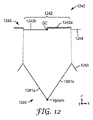
図12には、図11のフィルム1140と同じ、又は類似であり得る、両面光学フィルム1240の一部分の概略図が示されている。図12は、図11に比べて拡大されており、1248とラベル付けられた単一のプリズム/分離分散構造ペアを詳しく調べることができ、これは空気中にあると仮定される。図12のカーテシアン座標系は、図11及び前出の図の座標と一致している。フィルム1240は、一体型として示されているが、別の方法として、図11の層状構成を有してもよいし、別の層状構成を有してもよい。フィルム1240は、複数のプリズム1241が中に形成された第1構造化表面1243を有する。表面1243及びプリズム1241は、上述の対応する構造化表面1143及びプリズム1141と同じであり得る。この点に関して、プリズム1241は2つの傾斜側面又はファセット1241a、1241bを有し、これは、上述の対応する傾斜表面1141a、1141bと同じであり得る。表面1241a、1241bは交差してプリズム頂点Vprismを形成し、この頂点は、y軸に平行に伸びる線又は稜であり得る。
FIG. 12 shows a schematic view of a portion of a double-sided
フィルム1240は、複数の分離分散構造1242が中に形成された第2構造化表面1244も有する。表面1244及び分離分散構造1242は、上述の対応する構造化表面1144及び分離分散構造1142と同じであり得る。ゆえに、分離分散構造1242は、上述の部分1142bと同じであり得る低分散部分1242bに沿って配置された、上述の部分1142aと同じであり得る高分散部分1242aを有する。高分散部分1242aは、滑らかな低分散部分1242bに比べ、x−z面において粗面化された表面特性を有し、部分1242aは部分1242bに対して隆起している。分離分散構造1242の外側縁及びプリズム1241の外側縁は、点線の垂直線セグメントによって接続されて示されており、これは、プリズム/分離分散構造ペア1248の境界をしるすものと見なし得る。分離分散構造1242の幾何学的中心(x−z面の観点から)は、GCとラベル付けされている。幾何学的中心GC及びプリズム頂点Vprismは、分離分散構造1242に対するプリズム1241の整列(又はずれ)の度合を特性付けるための参照点として使用され得る。
The
図12A及び12Bは、図12のプリズム/分離分散構造ペア1248の複製であるが、その上に、広角出力ビーム(例えば図3を参照)及び狭角出力ビーム(例えば図4A又は4Bを参照)を生成するモードでの動作を示す光線を重ね合わせたものである。図12と同じ参照番号を有する品目は、それぞれ同じ要素を指し、これらについては更に述べる必要はない。
12A and 12B are duplicates of the prism / separation
図12Aにおいて、入射光線1234−2は、正のx方向に最も密接に揃った方向に沿って、フィルム1240の構造化表面1243に当たる。これは図3に類似している。入射光線1234−2は、斜めの光ビーム134−2(図3を参照)を適正に表している。光線1234−2は、例えば、x−z面内を伝搬し、かつx軸に対して約20±10度の角度をなす光線を、表わし得る。光線1234−2はプリズム1241の第1傾斜側面1241aに入る。この後、光線は、図に概ね示されているように、フィルム内を伝搬する。代表的な一実施形態において、フィルム1240の屈折率は1.67(中央の担体フィルム部分)及び1.51(プリズム及び分離分散構造部分)であり得、プリズム頂角は約60度であり得、高分散部分1242aの粗さ(Ra)は低分散部分1242bよりもかなり大きい値であり得、高分散部分1242aと低分散部分1242bとの間の垂直距離は25マイクロメートルであり得、幾何学的中心GCとプリズム頂点Vprismとの間の距離は113マイクロメートルであり得る。上記の値は、特定の一実施形態の単なる例示であり、不当に制限的に解釈されるべきではない。これらの仮定を用いて、斜めの光線1234−2は、図に概ね示されているように、フィルム1240内を通って伝搬する傾向にあり、光線1210Aにより表わされる出力ビームとしてフィルム1240から出る。光線1210Aは、広角出力ビーム310(図3)に類似の広角出力ビーム、又はその個々のビームレットのいずれかを提供する。フィルム1240は、主に分離分散構造1242の高分散部分1242aに向かって、斜めの入射光線1234−2を誘導する。これは、入射光線の一部が低分散部分1242bへと誘導され得、また入射光線の一部が、特定のプリズム/分離分散構造ペア1248の境界の外にある構造化表面1244の一部へと誘導され得ても、そのようになる。
In FIG. 12A, incident ray 1234-2 strikes structured
図12Bはその反対の場合であり、すなわち、狭角出力ビームを生成するモードの場合である。ここで、入射光線1232−2は、負のx方向に最も密接に揃った方向に沿って、フィルム1240の構造化表面1243に当たる。これは、図4A又は4Bに類似している。入射光線1232−2は、斜めの光ビーム132−2(図4A、4Bを参照)を適正に表している。光線1232−2は、例えば、x−z面内を伝搬し、かつ(負の)x軸に対して約20±10度の角度をなす光線を、表わし得る。光線1232−2はプリズム1241の第2傾斜側面1241bに入る。この後、光線は、図12Aと同じ設計特徴を仮定し、図12Bに概ね示されているように、フィルム内を伝搬する。これにより光線1232−2は、光線1210Bにより表わされる出力ビームとして、フィルム1240から出る。光線1210Bは、狭角出力ビーム410a(図4A)又は410b(図4B)に類似の狭角出力ビーム、あるいはその個々のビームレットのいずれかを提供する。フィルム1240は、主に分離分散構造1242の低分散部分1242bに向かって、斜めの入射光線1232−2を誘導する。これは、入射光線の一部が高分散部分1242aへと誘導され得、また入射光線の一部が、特定のプリズム/分離分散構造ペア1248の境界の外にある構造化表面1244の一部へと誘導され得ても、そのようになる。
FIG. 12B shows the opposite case, that is, the mode for generating a narrow-angle output beam. Here, the incident light ray 1232-2 strikes the structured
別の設計の代表的な両面光学フィルムを、図13、14、14A、及び14Bに示す。このフィルムは、上記のものと同じ又は類似の材料からなっていてよく、上記と同じ又は同様の製造技法及び設計特徴で製造することができる。 A representative double-sided optical film of another design is shown in FIGS. 13, 14, 14A, and 14B. The film may be made of the same or similar materials as described above and can be manufactured with the same or similar manufacturing techniques and design features as described above.
図13は、両面光学フィルム1340を示す。このフィルムは、相対する第1及び第2構造化表面1343、1344を有し、前の図と一致するカーテシアンx−y−z座標系で示されている。第1構造化表面1343は、複数のプリズム1341が中に形成されている。プリズム1341はそれぞれ、y軸に平行な伸長軸に沿って延在する。第2構造化表面1344は、複数の分離分散構造1342が中に形成されている。これらも、y軸に平行な伸長軸に沿って延在する。フィルム1340は、3つの構成層又は要素1345、1346、1347を有するが、これより多い又は少ない数の層も想到される。
FIG. 13 shows a double-sided
構造化表面1343の各プリズム1341は一般に、2つの傾斜側面又はファセット1341a、1341bを有する。これらの傾斜表面のうちのいくつかの隣接するペアが交差して、プリズム頂点を形成し、一方、他のペアが交差して、各プリズム1341の縁又は境界を形成する。図13には、頂点及び縁/境界の両方が、尖った又はV字形として示されているが、尖っていない、また非V字形の形状(例えば先端が切り取られた形状)も使用することができる。第1傾斜表面1341a及び第2傾斜表面1342bは両方とも、実質的に平坦である。別の実施形態においては、一方又は両方の表面が、x−z面内でわずかに湾曲していてもよい。プリズム1341は、ピッチp1によって特徴付けられ、これは、前述の実施形態のピッチp1と同じであっても異なっていてもよい。
Each
構造化表面1344の各分離分散構造1342は、高分散部分1342a及び低分散部分1342bが互いに沿って配置されている。この図において、高分散部分1342a及び低分散部分1342bの両方が、滑らかな表面によって特徴付けられ得る。しかしながら、高分散部分1342aは、図されるように実質的に平坦でありかつx−y面に平行であり得る低分散部分1342bに対して、x−z面内で大きく湾曲している。(高分散部分1342aの曲率が、図7の高分散部分742aの曲率とは反対であることに注意されたい。この分散部分1342aは正すなわち焦点を結ぶレンズレットであり、分散部分742aは負すなわち焦点を結ばないレンズレットである。)高分散部分1342aは、収束性又は凸面のレンズレットである。各分離分散構造について、高分散部分1342a及び低分散部分1342bは、分離分散構造の伸長軸に平行な(すなわち、y軸に平行な)境界に沿って接する。境界は、突然であっても徐々にであってもよい。分離分散構造1342は、ピッチp2によって特徴付けられ、これは、前述の実施形態のピッチp2と同じであっても異なっていてもよい。
Each separating and dispersing
図14には、図13のフィルム1340と同じ、又は類似であり得る、両面光学フィルム1440の一部分の概略図が示されている。図14は、図13に比べて拡大されており、1448とラベル付けられた単一のプリズム/分離分散構造ペアを詳しく調べることができ、これは空気中にあると仮定される。図14のカーテシアン座標系は、図13及び前出の図の座標と一致している。フィルム1440は、一体型として示されているが、別の方法として、図13の層状構成を有してもよいし、別の層状構成を有してもよい。フィルム1440は、複数のプリズム1441が中に形成された第1構造化表面1443を有する。表面1443及びプリズム1441は、上述の対応する構造化表面1343及びプリズム1341と同じであり得る。この点に関して、プリズム1441は2つの傾斜側面又はファセット1441a、1441bを有し、これは、上述の対応する傾斜表面1341a、1341bと同じであり得る。表面1441a、1441bは交差してプリズム頂点Vprismを形成し、この頂点は、y軸に平行に伸びる線又は稜であり得る。
FIG. 14 shows a schematic view of a portion of a double-sided
フィルム1440は、複数の分離分散構造1442が中に形成された第2構造化表面1444も有する。表面1444及び分離分散構造1442は、上述の対応する構造化表面1344及び分離分散構造1342と同じであり得る。ゆえに、分離分散構造1442は、上述の部分1342bと同じであり得る低分散部分1442bに沿って配置された、上述の部分1342aと同じであり得る高分散部分1442aを有する。高分散部分1442aは、低分散部分1442bに比べ、x−z面に大きく湾曲した表面を有する。分離分散構造1442の外側縁及びプリズム1441の外側縁は、点線の垂直線セグメントによって接続されて示されており、これは、プリズム/分離分散構造ペア1448の境界をしるすものと見なし得る。分離分散構造1442の幾何学的中心(x−z面の観点から)はGCとラベル付けされている。幾何学的中心GC及びプリズム頂点Vprismは、分離分散構造1442に対するプリズム1441の整列(又はずれ)の度合を特性付けるための参照点として使用され得る。
The
図14A及び14Bは、図14のプリズム/分離分散構造ペア1448の複製であるが、その上に、広角出力ビーム(例えば図3を参照)及び狭角出力ビーム(例えば図4A又は4Bを参照)を生成するモードでの動作を示す光線を重ね合わせたものである。図14と同じ参照番号を有する品目は、それぞれ同じ要素を指し、これらについては更に述べる必要はない。
14A and 14B are duplicates of the prism / separated
図14Aにおいて、入射光線1434−2は、正のx方向に最も密接に揃った方向に沿って、フィルム1440の構造化表面1443に当たる。これは図3に類似している。入射光線1434−2は、斜めの光ビーム134−2(図3を参照)を適正に表している。光線1434−2は、x−z面内を伝搬し、かつx軸に対して18度の角度をなす光線としてモデル化された。光線1434−2はプリズム1441の第1傾斜側面1441aに入る。光学的モデリングを使用して、この光線がこの後、フィルム内をどのように伝搬するかを決定した。モデリングは、次のように仮定された:フィルム1440の屈折率は、1.67(中央の担体フィルム部分)及び1.51(プリズム及び分離分散構造部分)であり、プリズム頂角は60度であり、高分散部分1442aの曲率半径は22.3マイクロメートルであり、幾何学的中心GCとプリズム頂点Vprismとの間の距離は113マイクロメートルであった。これらの仮定を使用して、光学モデリングが、フィルム1440を通る光線1434−2の軌跡を計算し、その結果が光線1410Aとして示されている。図14Aを確認することにより、光線1410Aは、広角出力ビーム310(図3)に類似の広角出力ビーム、又はその個々のビームレットのいずれかを提供していることがわかる。図14Aを確認することにより、フィルム1440が、主に分離分散構造1442の高分散部分1442aに向かって、斜めの入射光線1434−2を誘導していることが更にわかる。これは、入射光線の一部が低分散部分1442bへと誘導され、また入射光線の一部が、特定のプリズム/分離分散構造ペア1448の境界の外にある構造化表面1444の一部へと誘導されても、そのようになる。
In FIG. 14A, incident ray 1434-2 strikes structured
図14Bはその反対の場合であり、すなわち、狭角出力ビームを生成するモードの場合である。ここで、入射光線1432−2は、負のx方向に最も密接に揃った方向に沿って、フィルム1440の構造化表面1443に当たる。これは、図4A又は4Bに類似している。入射光線1432−2は、斜めの光ビーム132−2(図4A、4Bを参照)を適正に表している。光線1432−2は、x−z面内を伝搬し、かつ(負の)x軸に対して18±5度の角度をなす光線としてモデル化された。光線1432−2はプリズム1441の第2傾斜側面1441bに入る。光学的モデリングを使用して、この光線がこの後、フィルム内をどのように伝搬するかを決定した。このモデリングは、図14Aと同じ設計特徴を仮定した。これらの仮定を使用して、光学モデリングが、フィルム1440を通る光線1432−2の軌跡を計算し、その結果が光線1410Bとして示されている。図14Bを確認することにより、光線1410Bは、狭角出力ビーム410a(図4A)又は410b(図4B)に類似の狭角出力ビーム、あるいはその個々のビームレットのいずれかを提供していることがわかる。図14Bを確認することにより、フィルム1440が、主に分離分散構造1442の低分散部分1442bに向かって、斜めの入射光線1432−2を誘導していることが更にわかる。これは、入射光線の一部が高分散部分1442aへと誘導され、また入射光線の一部が、特定のプリズム/分離分散構造ペア1448の境界の外にある構造化表面1444の一部へと誘導されても、そのようになる。
FIG. 14B shows the opposite case, that is, the mode for generating a narrow-angle output beam. Here, incident light 1432-2 strikes the structured
以上、分離分散構造及びプリズムを組み込んだいくつかの両面光学フィルムについて記述してきたが、ここで、これらの要素をフィルムに組み合わせて、照明システムにおいて望ましい出力ビームを生成することが可能な様々な方法について詳しく説明していく。特に注目されるのは狭角出力ビームが生成される動作モードであるが、広角出力ビームも影響を受ける。フィルム内の各プリズム/分離分散構造ペアの設計詳細(プリズムと分離分散構造の垂直距離、これらの要素の相対的な横方向位置(横方向に整列されているか否か)、プリズムの傾き量(傾いている場合)、及び分離分散構造の傾き量(傾いている場合)など)は、所与の入力光ビームについて、所与のプリズム/分離分散構造ペアにより生成される出力ビーム又はビームレットの形状及びその他の特性を決定する。場合によっては、相対的な横方向位置及び/又は傾き量の変化といった設計パラメータは、フィルムの面上で変化し、フィルム中心においてある値を有し、フィルムの外縁又は端に向かって単調に増加又は減少させる。そのような空間的変化を使用して、図4Bの出力ビーム410bのような出力ビームを生成できる。また他の場合においては、関連する設計パラメータは、フィルムの面全体にわたって全て実質的に同じであってよく、これにより、全てのプリズム/分離分散構造ペアにより生成されるビーム又はビームレットは、実質的に同じになる。そのような空間的均一性を使用して、図4Aの出力ビーム410aのような出力ビームを生成できる。
Having described a number of double-sided optical films that incorporate separating and dispersing structures and prisms, various ways in which these elements can be combined with the film to produce the desired output beam in an illumination system. I will explain in detail. Of particular interest is the mode of operation in which a narrow-angle output beam is generated, but the wide-angle output beam is also affected. Design details of each prism / separation dispersion structure pair in the film (vertical distance between prism and separation dispersion structure, relative lateral position of these elements (whether they are aligned horizontally), prism tilt ( And the amount of tilt of the separating dispersion structure (such as tilting) for the given input light beam is that of the output beam or beamlet produced by the given prism / separating dispersion structure pair. Determine shape and other characteristics. In some cases, design parameters such as relative lateral position and / or change in tilt vary on the surface of the film, have a value at the film center, and increase monotonically toward the outer edge or edge of the film. Or decrease. Such spatial variation can be used to generate an output beam, such as
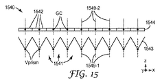
図15には、両面光学フィルム1540の概略図が示されている。フィルム1540は、第1構造化表面1543及び第2構造化表面1544を有し、第1構造化表面1543は、複数のプリズム1541が中に形成され、第2構造化表面1544は、複数の分離分散構造1542が中に形成されている。一般化のため、分離分散構造1542は、薄い箱型又は長方形が集合して構造化表面を形成するものとして、非常に模式的に示されている。読者には、これらの薄い箱型が、本明細書に開示される分離分散構造のいずれかを表わし得ることが理解されよう。フィルム1540は、カーテシアンx−y−z座標系で示されており、これは前の図と一致している。
FIG. 15 shows a schematic diagram of a double-sided
各プリズム1541は、頂点Vprismで交差する2つの傾斜側面又はファセットを含む。各プリズム1541は更に、プリズム光学軸1549−1を有する。プリズム光学軸1549−1はx−z面内にあり、プリズム頂点を通り、プリズム頂角を二等分し、その結果、両方の傾斜側面から等距離にある。プリズム1541は、x軸に沿った中心間(例えばプリズム頂点の間)のプリズムピッチp1によって特徴付けられるが、ピッチp1は、乱雑さを低減させるために図15にはラベル付けされていない。 Each prism 1541 includes two inclined sides or facets that intersect at the vertex Vprism. Each prism 1541 further has a prism optical axis 1549-1. The prism optical axis 1549-1 is in the xz plane, passes through the prism apex, bisects the prism apex angle, and as a result is equidistant from both inclined sides. The prism 1541 is characterized by a prism pitch p1 between the centers along the x-axis (eg, between the prism apexes), but the pitch p1 is not labeled in FIG. 15 to reduce clutter.
各分離分散構造1542は、高分散部分及び低分散部分を有するが、これらは図15には示されていない。各分離分散構造1542は、上述のように、幾何学的中心GCと、分散構造光学軸1549−2と、によって特徴付けられる。分散構造光学軸1549−2は、幾何学的中心GCを通過し、分離分散構造が実質的に対称である場合(例えば、図6及び10の分離分散構造642及び1042をそれぞれ参照)、分散構造光学軸1549−2は、分離分散構造1542の対称軸である。あるいは、分離分散構造に実質的な対称性がないが、高分散部分又は低分散部分のうちの一方又は両方が平坦である場合(例えば、図8、12、及び14の分離分散構造842、1242、1442をそれぞれ参照)、分散構造光学軸1549−2はそのような平坦表面に対して垂直である。あるいは、分離分散構造に実質的な対称性がなく、高分散部分及び低分散部分のいずれも平坦でない場合、分散構造光学軸1549−2は、分離分散構造1542のトポグラフィーに最適に適合する面に対して垂直である。分離分散構造1542は、x軸に沿った中心間(例えばGC間)の分離分散構造ピッチp2によって特徴付けられるが、ピッチp2は乱雑さを低減させるために図15にはラベル付けされていない。
Each separation and
フィルム1540において、構造化表面1543、1544はp1=p2となるように構成され、各プリズム頂点Vprismはそれぞれの分離分散構造のGCに垂直方向に整列しており、プリズム光学軸1549−1は互いにかつz軸に平行であり、分散構造光学軸1549−2も互いにかつz軸に平行である。よって、フィルム1540にある全てのプリズム光学軸1549−1及び全ての分散構造光学軸1549−2は、傾きゼロである。別の実施形態において、p1はここでもp2に等しくてよいが、プリズム頂点Vprismはそれぞれの分離分散構造GC点から望ましい量だけずれていてよく、そのため、出力ビームを特定の方向に向けることができる。
In
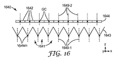
別の両面光学フィルム1640が図16に示されており、これは、図15のフィルムと同様の概略図である。フィルム1640は第1構造化表面1644及び第2構造化表面1644を有し、第1構造化表面1643は、複数のプリズム1641が中に形成されており、第2構造化表面1644は、複数の分離分散構造1642が中に形成されている。フィルム1640は、カーテシアンx−y−z座標系で示されており、これは前の図と一致している。
Another double-sided
各プリズム1641は、上述のように、頂点Vprismで交差する2つの傾斜側面又はファセットと、プリズム光学軸1649−1と、を含む。プリズム1641はプリズムピッチp1により特徴付けられるが、これは、乱雑さを低減させるために図16にはラベル付けされていない。
Each
各分離分散構造1642は、高分散部分及び低分散部分を有するが、これらは図16には示されていない。各分離分散構造1642は、上述のように、幾何学的中心GCと、分散構造光学軸1649−2と、によって特徴付けられる。分離分散構造1642は分散構造ピッチp2により特徴付けられるが、これは、乱雑さを低減させるために図16にはラベル付けされていない。
Each
フィルム1640において、構造化表面1643、1644はp1>p2となるように構成され、プリズム光学軸1649−1は互いにかつz軸に平行であり、分散構造光学軸1649−2も互いにかつz軸に平行である。よって、フィルム1640にある全てのプリズム光学軸1649−1及び全ての分散構造光学軸1649−2は、傾きゼロである。フィルム中央にあるプリズム/分離分散構造ペアについては(フィルムの左端から5つめであり、かつフィルム右端から5つめの頂点)、プリズム頂点Vprismは、それぞれの分離分散構造のGCと垂直に揃っている。しかしながら、フィルム上の他のプリズム/分離分散構造ペアについては、そのような垂直整列はなく、ずれの量はフィルム1640の中心からの距離が増大するに従って単調に増加している。図16に示される技法を使用して製造されたフィルム、又はより一般的にはp1≠p2であるフィルムは、例えば図4Bに示すように、出力光の中心分布が内側を指す又は内側を向いて、収束効果を生じるような効果を生み出すことができる。ずれの度合が大きいほど、クロストークのレベルが大きくなり、ずれの最大許容度は、特定の用途での最大許容クロストークレベルにより制限され得る。名目上揃っている特徴のペア(プリズム/分離分散構造ペア)が、隣接ペアに重なり合い始めたところで、クロストークが生じる。場合によっては、このような光方向付けアプローチは、フィルムの直角方向(z軸)と様々なプリズム/分離分散構造ペアの中央出力角との間が約10度以下の角度に制限され得る。この偏向角の制限は、厚さ(図18のDzを参照)、ピッチ、基板、含まれるプリズム角などのフィルムの幾何学的側面に依存する可能性があり、またライトガイドの出力分布により影響を受ける。
In
更に別の両面光学フィルム1740が図17に示されており、これは、図15及び16のフィルムと同様の概略図である。フィルム1740は、第1構造化表面1744及び第2構造化表面1744を有し、第1構造化表面1743は、複数のプリズム1741が中に形成されており、第2構造化表面1744は、複数の分離分散構造1742が中に形成されている。フィルム1740は、カーテシアンx−y−z座標系で示されており、これは前の図と一致している。
Yet another double-sided
各プリズム1741は、上述のように、頂点Vprismで交差する2つの傾斜側面又はファセットと、プリズム光学軸1749−1と、を含む。プリズム1741はプリズムピッチp1により特徴付けられるが、これは、乱雑さを低減させるために図17にはラベル付けされていない。
Each
各分離分散構造1742は、高分散部分及び低分散部分を有するが、これらは図17には示されていない。各分離分散構造1742は、上述のように、幾何学的中心GCと、分散構造光学軸1749−2と、によって特徴付けられる。分離分散構造1742は分散構造ピッチp2により特徴付けられるが、これは、乱雑さを低減させるために図17にはラベル付けされていない。
Each separation and
フィルム1740において、構造化表面1743、1744は、p1>p2となるように構成され、分散構造光学軸1749−2は互いにかつz軸に平行である。よって、フィルム1740にある全ての分散構造光学軸1749−2は、傾きゼロである(ただし、別の実施形態においては、例えば図19に参照されるように、ゼロではない傾きであってもよい)。しかしながら、プリズム光学軸1749−1は、フィルム上の位置に応じて傾斜し、中央のプリズム(フィルムの左端又は右端から5つめの頂点)は傾きゼロであり(z軸に平行)、中央プリズムの左にあるプリズムは正の傾きを有し、この傾きは、中央プリズムからの距離が増大するにつれて単調に増加し、中央プリズムの右にあるプリズムは負の傾きを有し、この傾きは、中央プリズムからの距離が増大するにつれて(傾き量が)単調に増加する。ここで、正の傾きは時計方向の傾きを指し、負の傾きは反時計方向の傾きを指す。中央プリズムのプリズム頂点Vprismは、対応する分離分散構造のCGに垂直整列しているが、フィルム上の他のプリズム/分離分散構造ペアについては、そのような垂直整列は生じず、ずれの度合は、フィルム1740の中央からの距離が増大するにつれて単調に増加する。図17に示される技法を使用して製造されたフィルム、又はより一般的には、プリズム及び/又は分離分散構造が傾いているフィルムは、例えば図4Bに示すように、出力光の中心分布が内側を指す又は内側を向いて、収束効果を生じるような効果を生み出すことができる。上述のように、ずれの度合が大きいほど、クロストークのレベルが大きくなり、ずれの最大許容度は、特定の用途での最大許容クロストークレベルにより制限され得る。場合によっては、このような光方向付けアプローチは、フィルムの直角方向(z軸)と様々なプリズム/分離分散構造ペアの中央出力角との間が約35度以下の角度に制限され得る。この偏向角の制限は、厚さ(図18のDzを参照)、ピッチ、基板、含まれるプリズム角などのフィルムの幾何学的側面に依存する可能性があり、またライトガイドの出力分布により影響を受ける。この整列技法についての更なる詳細は、米国特許出願公開第US 2012/0236403号(Sykoraら)も参照される。
In
更に別の代替設計において、図15、16、及び17のうちのいずれかの分離分散構造は、例えば、フィルム上の位置に応じて変化する様相で、任意の望ましいやり方で傾けることができ、例えば、フィルムの中央では傾きゼロであり、中央からフィルムの左端に行くに従って正の傾きが増大し、また中央からフィルムの右端に行くに従って負の傾きが増大し得る。 In yet another alternative design, the separating and dispersing structure of any of FIGS. 15, 16, and 17 can be tilted in any desired manner, eg, in a manner that varies depending on the position on the film, In the middle of the film, the slope is zero, and the positive slope increases from the center to the left edge of the film, and the negative slope increases from the center to the right edge of the film.
図18及び19は、両面光学フィルム内に存在し得る別のプリズム/分離分散構造ペアの拡大図を示す。図18では、ペアの要素は互いに平行移動的及び回転移動的に揃っている。図19では、これら要素は互いに平行移動的及び回転移動的にずれており、異なる量の傾きを有している。これらの図の両方において、一般化のため、図15〜17と同様に、分離分散構造は、薄い箱型又は長方形によって、模式的に示されている。 18 and 19 show enlarged views of another prism / separated dispersion structure pair that may be present in a double-sided optical film. In FIG. 18, the elements of a pair are aligned in translation and rotation. In FIG. 19, these elements are offset from each other in translational and rotational movement and have different amounts of slope. In both of these figures, for the sake of generalization, the separation / distribution structure is schematically shown by a thin box shape or rectangle as in FIGS.
図18では、プリズム/分離分散構造ペア1848は、1つのプリズム1841と1つの分離分散構造1842と、を有する。プリズム1841は、頂点Vprismで接する傾斜側面又はファセット1841a、1841bを有する。プリズム1841は更に、上述のように、プリズム光学軸1849−1を有する。分離分散構造1842は、上述のように、幾何学的中心GC及び分散構造光学軸1849−2を有する。フィルム厚さ及び/又はコーティング厚さを適切に選択することにより、構造1842のプリズム焦点とGCとの間の垂直距離Dzは、望ましい光学的性能の出力ビームを得られるように制御することができる。Dzの光学的値を決定するには、通常、光学フィルムの屈折率も考慮に入れる。光学軸1849−1、1849−2は互いに平行かつz軸に対して平行であり、互いに揃っている。
In FIG. 18, the prism / separation
図19では、プリズム/分離分散構造ペア1948は、1つのプリズム1941と1つの分離分散構造1942と、を有する。プリズム1941は、頂点Vprismで接する傾斜側面又はファセット1941a、1941bを有する。プリズム1941は更に、上述のように、プリズム光学軸1949−1を有する。分離分散構造1942は、上述のように、幾何学的中心GC及び分散構造光学軸1949−2を有する。フィルム厚さ及び/又はコーティング厚さを適切に選択することにより、構造1942のプリズム焦点とGCとの間の垂直距離Dzは、望ましい光学的性能の出力ビームを得られるように、また、光学フィルムの屈折率も考慮に入れて、制御することができる。分離分散構造1942は、x軸に沿ったずれ量Dxだけ、プリズム1941に対して平行移動的にずれている。分離分散構造1942は更に、プリズム1941に対して回転移動的にもずれている。分散構造光学軸1949−2は、プリズム光学軸1949−1に対してx−z面において傾いており、更に、分散構造光学軸1949−2及びプリズム光学軸1949−1の両方が、z軸に対して傾いている。図に示すように、分散構造光学軸及びプリズム光学軸の傾き角を参照するために、角α及びβを使用することができる。本明細書に開示される両面光学フィルムは、設計パラメータDz、Dx、α、及びβを適切に利用することができ、これらはフィルム面積にわたって(全てのプリズム/分離分散構造ペアについて)均一であってもよいし、又はそのような面積にわたって不均一であってもよく、これによって、1つの光源がオンのときに広角出力ビームを提供し、別の光源がオンの時に狭角出力ビームを提供することができる。
In FIG. 19, the prism / separation
図20A及び20Bは、本開示の両面光学フィルムに関連する理想化した分布を示すグラフである。これらの図の曲線は実際のデータではなく、好適に調節した両面光学フィルムを含む光学システムの考えられる動作を理想化したものとして示している。これらの図は、極角θに応じたx−z面内の相対的光強度をグラフにしたものであり、ここでθは、空気中の光の伝搬方向とz軸との間の角である。図20Aでは、光学システムの1つの光源(例えば図3の光源134)がオンであり、別の光源がオフである。光源からの光は、非常に斜めの光の入力ビーム2034−2として光学フィルムに供給される。例えば、図3の斜めの光ビーム134−2を参照されたい。この入力ビームは、プリズムの第1傾斜表面を通って両面光学フィルムに入るが、この第1傾斜表面は、分離分散構造の高分散部分に主に関連している。したがって、このビームは広角出力ビーム2010Aとしてフィルムから出る。曲線2010Aは、両面光学フィルムの面積全体にわたる光出力を表わすが、フィルムの各プリズム/分離分散構造ペアから出る個々のビーム又はビームレットそれぞれも表わし得る。
20A and 20B are graphs showing idealized distributions associated with the double-sided optical film of the present disclosure. The curves in these figures are not actual data, but represent idealized operation of an optical system that includes a well-adjusted double-sided optical film. These figures are graphs of the relative light intensity in the xz plane according to the polar angle θ, where θ is the angle between the propagation direction of light in the air and the z axis. is there. In FIG. 20A, one light source (eg,
図20Bでは、反対側の光源(例えば図4A又は4Bの光源132)がオンである。この光源からの光は、非常に斜めの光の入力ビーム2032−2として光学フィルムに供給される。例えば、図4A又は4Bの斜めの光ビーム132−2を参照されたい。この入力ビームは、プリズムの第2傾斜表面を通って両面光学フィルムに入るが、この第2傾斜表面は、分離分散構造の低分散部分に主に関連している。したがって、このビームは狭角出力ビーム2010Bとしてフィルムから出る。曲線2010Bは、両面光学フィルムの面積全体にわたる光出力を表わすが、フィルムの各プリズム/分離分散構造ペアから出る個々のビーム又はビームレットそれぞれも表わし得る。プリズム及び/又は分離分散構造の光学軸を傾けることにより、並びに/あるいは、プリズムとそれに関連する分離分散構造とをずらすことにより、狭角出力ビームを調節して、フィルムに対して直角ではない主方向に沿って、フィルムから出るようにすることができる。例えば、代替の狭角出力ビーム2010B’及び2010B”を参照されたい。
In FIG. 20B, the opposite light source (eg,
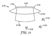
図21は、代表的な両面光学フィルムを利用したディスプレイシステム2100の概略図である。このシステムは、1つ以上の第1光源2134、1つ以上の第2光源2132、バックライトパッケージ2130、及びディスプレイパネル(図示なし)を含む。光源2134、2132は、上述の光源134、132と同じであるか、又はこれと類似し得る。バックライトパッケージ2130は、例えば図1A及び1Bのように配列された、少なくとも1つのライトガイドと1つの両面光学フィルムとを含む。両面光学フィルムは、本明細書に記載される設計特性のいずれかを、この用途に好適に調節して有し得る。これらの設計特性に関する前述の議論に従って、この両面光学フィルムは、第1動作モードにおいて、第1光源2134がオンであり第2光源2132がオフのときに、広角出力ビーム2110Aを提供し、第2動作モードにおいて、第2光源2132がオンであり第1光源2134がオフのときに、狭角出力ビーム2110Bを提供するよう設計される。システム2100は望ましくは、第1動作モードから第2動作モードに、又はその逆に変更するようユーザーが作動できるスイッチを含む。第1動作モードでは、広角出力ビーム2110Aが提供され、これによって中央にいる観測者2102だけでなく、周辺にいる観測者2103、2104も、ディスプレイを見ることができる。これは、システム2130のパブリックビューイング動作モードと見なすことができる。第2動作モードでは、狭角出力ビーム2110Bが提供され、これによって中央にいる観測者2102はディスプレイを見ることができるが、周辺にいる観測者2103、2104には見ることができない。これは、システム2130のプライベートビューイング動作モードと見なすことができる。このように、システム2100は、電子的に切り替え可能なプライバシー機能を有することができる。
FIG. 21 is a schematic view of a
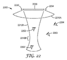
図22のディスプレイシステム2200は、図21と類似しているが、両面光学フィルムは、狭角出力ビームが光学フィルムから出る際に収束するよう調節されている。ゆえに、システム2200は、代表的な両面光学フィルムを利用し、1つ以上の第1光源2234、1つ以上の第2光源2232、バックライトパッケージ2230、及びディスプレイパネル(図示なし)を含む。光源2234、2232は、図21の光源2134、2132と同じであるか、又はこれと類似し得る。バックライトパッケージ2230は、図21のバックライトパッケージ2130と類似し得るが、ただし、この両面光学フィルムは、個々のプリズム/分離分散構造ペアが、光学フィルムの出力領域にわたって異なる方向に配向されたビーム又はビームレットを生成するよう、構成されている。例えば図4Bを参照されたい。第1動作モードでは、両面光学フィルムは、第1光源2234がオンであり第2光源2232がオフのとき、広角出力ビーム2210Aを提供する。第2動作モードでは、両面光学フィルムは、第2光源2232がオンであり第1光源2234がオフのとき、狭角出力ビーム2210Bを提供する。図示のように、狭角出力ビームは、光学フィルムから出る際に最初に収束して、ビームウェスト2210B’で最小ビーム幅を達成し、ここを超えるとビーム2210Bが発散する。システム2100と同様に、システム2200は、望ましくは、第1動作モードから第2動作モードに、又はその逆に変更するようユーザーが作動できるスイッチを含む。第1動作モードの広角出力ビーム2210Aによって、中央にいる観測者2202だけでなく、周辺’にいる観測者2203、2204も、ディスプレイを見ることができる。第2動作モードの狭角出力ビーム2210Bによって、中央にいる観測者2202はディスプレイを見ることができるが、周辺にいる観測者2203、2204には見ることができない。このように、システム2200も、電子的に切り替え可能なプライバシー機能を有することができる。中央にいる観測者2202は、システム2200の中央の観測軸から偏向しすぎないかぎり(これは、出力ビーム2210Bによって画定され得る)、他の観測位置でもディスプレイを引き続き見ることができる(例えば観測者2202’を参照)。
The
図21及び22の機能及び原理は、ディスプレイシステム以外に、照明システムにも適用することができる。図23及び24において、これらの原理は、その機能が、部屋、オフィス、又はその他の居住空間を照らすことである照明システムに適用される。図23の照明システム2300は、ディスプレイパネルが除去されていること以外は、図21のディスプレイシステム2100と類似し得る。よって、システム2300は、1つ以上の第1光源、1つ以上の第2光源、ライトガイド、及び両面光学フィルムを含む。光源は、上述の他の光源と同じであるか、又はこれに類似し得る。両面光学フィルムは、本明細書で説明される設計特性のいずれかを、この用途に好適に調節して有することができる。この両面光学フィルムは、第1動作モードにおいて、第1光源がオンであり第2光源がオフのときに、広角出力ビーム2310Aを提供し、第2動作モードにおいて、第2光源がオンであり第1光源がオフのときに、狭角出力ビーム2310Bを提供するよう設計される。システム2300は、望ましくは、第1動作モードから第2動作モードに、又はその逆に変更するようユーザーが作動できるスイッチを含む。第1動作モードでは、広角出力ビーム2310Aが提供され、これは部屋又は居住空間の広い面積を幅広く照らす。システム2300は、床2305及び占有者2302がいる部屋の天井に取り付けられて示されている。第2動作モードでは、狭角出力ビーム2310Bが提供され、これは部屋のかなり小さな部分を照らす。第1モードの幅広い照明に比べ、この狭角照明は、スポットライト出力を提供するものと見なすことができる。このように、システム2300は、電子的に切り替え可能なスポットライト機能を有することができる。
The functions and principles of FIGS. 21 and 22 can be applied to lighting systems in addition to display systems. In FIGS. 23 and 24, these principles apply to a lighting system whose function is to illuminate a room, office, or other living space. The
図24の照明システム2400は、図23と類似しているが、両面光学フィルムは、狭角出力ビームが光学フィルムから出る際に収束するよう調節されている。これは、第2動作モードのスポットライト効果を更に提供することができる。よって、システム2400は、1つ以上の第1光源、1つ以上の第2光源、ライトガイド、及び両面光学フィルムを利用する。これらの品目はシステム2300の対応する項目と同じ又は類似し得るが、ただし、この両面光学フィルムは、個々のプリズム/分離分散構造ペアが、光学フィルムの出力領域にわたって異なる方向に配向されたビーム又はビームレットを生成するよう、構成されている。例えば図4Bを参照されたい。第1動作モードでは、両面光学フィルムは、第1光源がオンであり第2光源がオフのとき、広角出力ビーム2410Aを提供する。第2動作モードでは、両面光学フィルムは、第2光源がオンである第1光源がオフのとき、狭角出力ビーム2410Bを提供する。図示のように、狭角出力ビームは、光学フィルムから出る際に最初に収束して、ビームウェスト2410B’で最小ビーム幅を達成し、ここを超えるとビーム2410Bが発散する。システム2300と同様に、システム2400は、望ましくは、第1動作モードから第2動作モードに、又はその逆に変更するようユーザーが作動できるスイッチを含む。第1動作モードでは、広角出力ビーム2310Aは、部屋又は居住空間の広い面積を幅広く照らす。システム2400は、床2405、テーブル又はその他の高くなった表面2406、及び占有者2402がいる部屋の天井に取り付けられて示されている。第2動作モードでは、狭角出力ビーム2410Bは、部屋のかなり小さな部分を照らす。第1モードの幅広い照明に比べ、この狭角照明は、スポットライト出力を提供するものと見なすことができる。ビームウェスト2410B’は、システム2400から軸距離fの位置にあり、両面光学フィルムは、ビームウェスト2410B’が望ましい軸方向位置(例えば床2405の上、又はテーブル2406の高さ)に配置されるように調節することができる。このように、システム2400は、電子的に切り替え可能なスポットライト機能を有することができる。
The
開示の両面光学フィルム、ライトガイド、及び関連構成要素に、数多くの改変を行うことができ、また数多くの機能を組み込むことができる。例えば、両面光学フィルム又はライトガイドの任意の構造化表面は、空間的に均一であってよく、すなわち、構造化表面の個々の要素又は構造は、構成要素の主表面全体を占める繰り返しパターンを形成し得る。例えば、図1B及び2を参照のこと。あるいは、任意のそのような構造化表面は、構造化表面の一部分がそのような個々の要素又は構造を含まないか、あるいは、その一部分がそのような個々の要素又は構造を含むが、そのような要素又は構造は、完全又は部分的に作動しないようになっている様相で、パターン化されていてもよい。構造化表面の一部分において、そのような個々の要素又は構造が欠落した状態は、まず全主表面にわたって要素又は構造を形成し、次に任意の好適な技法によって破壊又はその他の方法で除去することによって(例えば、十分な熱及び/又は圧力を適用して、望ましい部分の要素又は構造を(パターンによって)選択的に平らにすることによって)、達成することができる。あるいは、個々の要素又は構造が欠落した状態は、構造化表面の他の領域で要素又は構造化表面が形成されているときに(例えば好適にパターン化されたツールを使用して)、構造化表面の望ましい部分にこれらを形成しないことにより、達成することができる。個々の要素又は構造が、構造化表面の望ましい部分で完全又は部分的に作動できないようにされた場合は、その構造化表面は最初は空間的に均一であり得るが、個々の要素又は構造は、次いで、接着剤、印刷媒体、あるいは屈折率がその要素若しくは構造の屈折率に合致する(実質的に合致する場合を含む)ような好適な材料で、又は少なくとも空気若しくは真空とは異なる屈折率を有するようなその他の好適な材料で、パターンを用いた方法でコーティング又は他の方法で被覆することができる。そのようなパターンを用いて適用された材料は、構造化表面に適用した後に硬化又は架橋させてもよく、構造化表面の望ましい部分を平坦化することができる。個々の要素又は構造が欠落している、又は作動しないようにされているかどうかを問わず、光学システムは、1つのみの構造化表面(例えばライトガイドの構造化表面、又は両面フィルムの構造化表面)がパターン化されているか、又は2つのみの構造化表面がパターン化されているか、又は3つのみの構造化表面がパターン化されているか、又は4つの構造化表面がパターン化されるよう、設計できる。2つを超える構造化表面がパターン化される場合、任意の2つのパターン化表面に同じパターンを使用してもよいし、異なるパターンを使用してもよい。 Numerous modifications can be made and many features can be incorporated into the disclosed double-sided optical film, light guide, and related components. For example, any structured surface of a double-sided optical film or light guide may be spatially uniform, i.e., individual elements or structures of the structured surface form a repeating pattern that occupies the entire major surface of the component. Can do. See, for example, FIGS. 1B and 2. Alternatively, any such structured surface may be such that a portion of the structured surface does not include such individual elements or structures, or a portion thereof includes such individual elements or structures. The elements or structures may be patterned in such a way that they are not fully or partially activated. The absence of such individual elements or structures in a portion of the structured surface must first form elements or structures across the entire major surface and then be destroyed or otherwise removed by any suitable technique. (E.g., by applying sufficient heat and / or pressure to selectively flatten (by a pattern) the desired portion of the element or structure). Alternatively, the absence of individual elements or structures can be caused by structuring when elements or structured surfaces are formed in other areas of the structured surface (eg, using a suitably patterned tool). This can be achieved by not forming these in the desired portion of the surface. If an individual element or structure is rendered inoperable completely or partially at a desired portion of the structured surface, the structured surface may initially be spatially uniform, but the individual element or structure is Then a suitable material, such as an adhesive, a print medium, or a refractive index that matches (including substantially matches) the refractive index of the element or structure, or at least a refractive index different from air or vacuum Other suitable materials, such as, can be coated or otherwise coated in a pattern-based manner. The material applied using such a pattern may be cured or cross-linked after application to the structured surface and can planarize the desired portion of the structured surface. Regardless of whether individual elements or structures are missing or rendered inoperative, the optical system can only have one structured surface (for example, a light guide structured surface or a double-sided film structured). Surface) is patterned, or only two structured surfaces are patterned, or only three structured surfaces are patterned, or four structured surfaces are patterned Can be designed. Where more than two structured surfaces are patterned, the same pattern may be used for any two patterned surfaces, or different patterns may be used.
別の方法においては、好適に設計されたライトガイドを用いて、2枚の両面光学フィルムを、ライトガイドの相対する側に使用することができる。ライトガイドは、その相対する主表面それぞれから斜めの光ビームを提供するよう構成され、更に、両面フィルム1枚を、ライトガイドの各主表面に提供して、上述のように、どちらの光源がオンになっているかに応じて、斜めの光ビームを広角出力ビーム又は狭角出力ビームに変換することができる。例えば、図1Bでは、フィルム140の鏡像(x−y面に対して)である両面フィルムを、ライトガイド150の反対側に配置して、これによりライトガイドが2枚の鏡像両面光学フィルムの間に配置されるようにすることができる。
In another method, with a suitably designed light guide, two double-sided optical films can be used on opposite sides of the light guide. The light guide is configured to provide an oblique light beam from each of its opposing main surfaces, and further, a double-sided film is provided on each main surface of the light guide, as described above, which light source Depending on whether it is on, the oblique light beam can be converted into a wide-angle output beam or a narrow-angle output beam. For example, in FIG. 1B, a double-sided film that is a mirror image of the film 140 (relative to the xy plane) is placed on the opposite side of the
別の方法としては、光学システムは更に、両面光学フィルムによって生成される出力ビームの光拡散の度合を制限又は低減するための、二次的構造を含んでもよい。例えば、従来型の覗き見防止ルーバーフィルム及び/又はシュラウド(例えば1つ以上の光ブロック部材を含む)を、両面フィルムの出力側に設けることができる。これらの二次的構造は、x−z面及び/又はy−z面内で(例えば、図3、4A、4Bのx−y−z座標方向を参照)、所与の初期出力ビームの一部分を塞ぐことによって操作することができ、これによって改変された出力ビームが生成され、この改変された出力ビームは、閉塞面の初期出力ビームよりも狭角になる。 Alternatively, the optical system may further include a secondary structure to limit or reduce the degree of light diffusion of the output beam produced by the double-sided optical film. For example, a conventional peep prevention louver film and / or shroud (eg, including one or more light blocking members) can be provided on the output side of the double-sided film. These secondary structures are part of a given initial output beam in the xz and / or yz planes (see, eg, the xyz coordinate directions of FIGS. 3, 4A, 4B). Can be manipulated to produce a modified output beam that is narrower than the initial output beam of the occlusion surface.
このライトガイド及び両面光学フィルムは両方とも、全体的な形状が実質的に平面であってよく、又は一方若しくは両方が非平面であってもよい。代表的な照明システムの実施形態の概略図が、図25A〜25Eに示されている。これらの図のそれぞれにおいて、第1光源2534及び第2光源2532は、伸長した本体の相対する縁に沿って提供される。光源2534、2532は、上述の光源134、132と同じであるか、又はこれと類似し得る。伸長した本体は、図25AにおいてEBa、図25BにおいてEBb、図25CにおいてEBc、図25DにおいてEBd、及び図25EにおいてEBeとしてラベル付けされており、これらは、ライトガイド、両面光学フィルム、又は両方を表わし得る。これらの図の伸長した本体は、前の図と一致する、カーテシアンx−y−z座標系で示されている。平面からの逸脱は、可撓性の伸長した本体を示すものであり得、あるいは、非平面形状に形成された物理的に剛性の伸長した本体を示すものであり得る。伸長した本体EBaは、実質的に平面的であり、x−y面に平行に延在する。伸長した本体EBbは非平面的であり、y−z面内で湾曲しているが、x−z面では湾曲していない。伸長した本体EBcも非平面的であり、x−z面内で湾曲しているが、y−z面では湾曲していない。別の実施形態では、x−z面とy−z面の両方での湾曲を有し得る。伸長した本体EBdは非平面的であり、y−z面内で湾曲しているがx−z面では湾曲しておらず、y−z面での湾曲は、本体自体が閉じて、管状構造を形成するようになっている。この管状構造は、図示するように、長手方向のスロット又は隙間を含み得る。この管状構造は、横断面(例えば、y−z面の断面)において実質的に円形であってよく、あるいは、楕円形又はその他の非円形であってもよい。伸長した本体EBdは非平面的であるが、x−z面内で湾曲しているがy−z面では湾曲しておらず、x−z面での湾曲は、本体自体が閉じて、管状構造を形成するようになっている。この管状構造は、図示するように、長手方向のスロット又は隙間を含み得る。この管状構造は、横断面(例えば、x−z面の断面)において実質的に円形であってよく、あるいは、楕円形又はその他の非円形であってもよい。図25A〜25Eの形状のいずれかを有する照明システムは、任意の望ましい形状要素に構築することができ、これには、従来型の電球に類似の形状要素が含まれ得、また、切り替え可能な広角/狭角出力ビーム分布の付加的機能を伴って、従来型の電球の代わりに使用することができる。
Both the light guide and the double-sided optical film may be substantially planar in overall shape, or one or both may be non-planar. A schematic diagram of an exemplary lighting system embodiment is shown in FIGS. In each of these figures, a
図5及び6に示すものに類似した両面光学フィルムを、光学設計ソフトウェアを用いてモデル化した。このフィルムは、図6A及び6Bに関連して上述された設計特性を有するものと想定され、すなわち:フィルムの屈折率は1.67(中央の担体フィルム部分)及び1.51(プリズム及び分離分散構造部分)であり、プリズム頂角は約60度であり、湾曲セグメントの公称曲率半径(この半分は粗面化されている)は約41マイクロメートルであり、分離分散構造の幾何学的中心GCとプリズム頂点Vprismとの間の距離は111マイクロメートルであり、高分散部分の表面粗さ(Ra)は約0.588マイクロメートルであった。この両面フィルムに隣接するライトガイドは、第1光源のみの通電に伴う第1入力ビーム、及び、第2光源のみの通電に伴う第2入力ビームとしてモデル化され、これらの入力ビームは、両面フィルムのプリズム側に当たるようにされた。これらの入力ビームの一方は、x−z面を伝搬し(座標系の向きについては図5及び6を参照)、かつ(正の)x軸に対して20±10度の角度をなす光線としてモデル化され、他方の入力ビームは、x−z面を伝搬し、かつ(負の)x軸に対して20±10度の角度をなす光線としてモデル化された。第1光源がオンであり、第2光源がオフであるとき、このシステムが生成する出力ビームの、極角(すなわちz軸に対する角)に応じたx−z面の分布が、図26の曲線2601として示されている。第1光源がオフであり、第2光源がオンであるとき、このシステムが生成する出力ビームのx−z面の分布が、曲線2602として示されている。曲線2601の出力ビームは、曲線2602の出力ビームよりも広角である。曲線2601の形状を更に改変して、両面フィルムの設計詳細を適切に最適化することにより、単一の幅広の釣鐘型の輪郭を有する分布を提供することができることが予想される。
A double-sided optical film similar to that shown in FIGS. 5 and 6 was modeled using optical design software. This film is assumed to have the design characteristics described above in relation to FIGS. 6A and 6B, ie: the refractive index of the film is 1.67 (middle carrier film portion) and 1.51 (prism and separation dispersion) The prism apex angle is about 60 degrees, the nominal radius of curvature of the curved segment (half of which is roughened) is about 41 micrometers, and the geometric center GC of the separating dispersion structure The distance between the prism vertex Vprism and the prism vertex Vprism was 111 micrometers, and the surface roughness (Ra) of the high dispersion portion was about 0.588 micrometers. The light guide adjacent to the double-sided film is modeled as a first input beam accompanying energization of only the first light source and a second input beam accompanying energization of only the second light source. It was made to hit the prism side. One of these input beams propagates in the xz plane (see FIGS. 5 and 6 for the orientation of the coordinate system) and as a ray that makes an angle of 20 ± 10 degrees with respect to the (positive) x-axis. The other input beam was modeled as a ray propagating in the xz plane and making an angle of 20 ± 10 degrees with respect to the (negative) x axis. When the first light source is on and the second light source is off, the distribution of the xz plane of the output beam generated by this system as a function of the polar angle (ie, the angle with respect to the z axis) is the curve of FIG. 2601 is shown. When the first light source is off and the second light source is on, the xz plane distribution of the output beam produced by this system is shown as
別の両面光学フィルムが、光学設計ソフトウェアでモデル化された。このフィルムの設計は、図7及び8に示す設計と類似していた。このフィルムは、図8A及び8Bに関連して上述された設計特性を有するものと想定され、すなわち:フィルム840の屈折率は、1.67(中央の担体フィルム部分)及び1.51(プリズム及び分離分散構造部分)であり、プリズム頂角は約63.5度であり、プリズム表面の曲率半径は160マイクロメートルであり、高分散部分の曲率半径は30マイクロメートルであり、幾何学的中心GCとプリズム頂点Vprismとの間の距離は113マイクロメートルであった。プリズムの傾斜側面の一方に光線を入射することにより、第1の斜めの入力光ビーム(第1光源がオンであり第2光源がオフである場合に相似)がシミュレーションされた。入射光線は、以下の角範囲にわたって分散した:x−z面の光線投射(座標の向きについては図7及び8を参照)は正のx構成要素を有し、z軸に対して62〜82度(72±10度)の角度をなし、y−z面の光線投射は正のz構成要素を有し、z軸に対して−40〜+40度(0±40度)の角度をなした。両面光学フィルムは、この第1の斜め入力ビームを第1出力ビームに変換し、そのx−z面における分布は、極角に応じて、図27の相対的強度の曲線2701として示されている。次に、プリズムの他方の傾斜表面に光線を入射することにより、第2の斜めの入力光ビーム(第1光源がオフであり第2光源がオンである場合に相似)がシミュレーションされた。入射光線は、以下の角範囲にわたって分散した:x−z面における光線投射は負のx構成要素を有し、z軸に対して62〜82度(72±10度)の角度をなし、y−z面における光線投射はやはり正のz構成要素を有し、ここでもz軸に対して−40〜+40度(0±40度)の角度をなした。両面光学フィルムは、この第2の斜め入力ビームを第2出力ビームに変換し、そのx−z面にける分布は、極角に応じて、図27の相対的強度の曲線2702として示されている。第1出力ビーム(曲線2701)の光の分散は、第2出力ビーム(曲線2702)に比べて広いことに注意されたい。第1出力ビームは、x−z面の半値全幅(FWHM)として測定された場合に、55度の角分散を有し、第2出力ビームは、(同様に測定された場合に)11度の核分散を有している。
Another double-sided optical film was modeled with optical design software. The design of this film was similar to the design shown in FIGS. This film is assumed to have the design characteristics described above in connection with FIGS. 8A and 8B, ie: the refractive index of
極角度及び方位角の両方に応じて、両面フィルムにより光がどのように放射されるかを示すには、コノスコーププロットが便利である。コノスコーププロットに密接に関係するのは等カンデラ極グラフである。これは、同様の便利な角度情報を提供するが、ただし、強度値は、等カンデラ極グラフにおいてはコサイン修正されていない。しかしながら、強度値を極角度のコサインで割ることにより、相対輝度データを得ることができる。このモデル化された両面光学フィルムの第1出力ビームの等カンデラ極グラフを図28Aに、また第2出力ビームの等カンデラ極グラフを図28Bに示す。これらのプロットにおいて、z軸は円スケールの中心点に対応し、極角度(z軸に対する角度)はこの中心点からの径距離に対応し、方位角(y軸に対する角度)は、円スケールの円周にある数0、15、30、45、...345によって示されている。計算された相対的光強度は、各点においてグレースケールの陰影で示されている。グラフ上の濃い色の点は、より明るい光を示し、これは、相対的強度を示す左側の線形尺度によって提供されている。第2出力ビーム(図28B)に比べて、第1出力ビーム(図28A)のほうが、x−z面(方位角90度及び270度)において、より幅広い光分散を提供していることに注意されたい。
A conoscopic plot is useful to show how light is emitted by a double-sided film, depending on both polar and azimuthal angles. Closely related to the conoscopic plot is the isocandela polar graph. This provides similar useful angle information, except that the intensity values are not cosine corrected in the iso-candela polar graph. However, relative luminance data can be obtained by dividing the intensity value by the cosine of the polar angle. FIG. 28A shows an equal candela polar graph of the first output beam of this modeled double-sided optical film, and FIG. 28B shows an equal candela polar graph of the second output beam. In these plots, the z-axis corresponds to the center point of the circular scale, the polar angle (angle relative to the z-axis) corresponds to the radial distance from this center point, and the azimuth angle (angle relative to the y-axis) is the circular scale The
特に指定されないかぎり、本明細書及び特許請求の範囲において使用される、数量、特性の測定値などを表す全ての数値は、「約」という語で修飾されるものとして理解されるべきである。したがって、反することが示されないかぎり、本明細書及び特許請求の範囲に記載の数値的パラメータは、本願の教示を利用して当業者により得ることが求められる所望の性質に応じて変化し得る近似値である。特許請求の範囲に対する均等論の適用を制限しようとするものではないが、各数値パラメータは、少なくとも記載される有効桁数を考慮し、更に一般的な四捨五入法を適用することによって解釈されるべきである。本発明の広義の範囲を示す数値的範囲及びパラメータは近似的な値であるが、任意の数値が本明細書に述べられる具体例に記載されるかぎりにおいては、これらは妥当な程度に可能な範囲で正確に記載されるものである。しかしながら、いかなる数値も、試験又は測定の限界に伴う誤差を含み得る。 Unless otherwise specified, all numerical values used in the specification and claims, such as quantities, measurements of properties, etc., are to be understood as being modified by the word “about”. Accordingly, unless indicated to the contrary, the numerical parameters set forth in the specification and claims are approximations that may vary depending on the desired properties sought to be obtained by one skilled in the art using the teachings herein. Value. Although not intended to limit the application of the doctrine of equivalents to the claims, each numeric parameter should be interpreted by taking into account at least the significant digits listed and applying a more general rounding method It is. The numerical ranges and parameters indicating the broad scope of the present invention are approximate, but as long as any numerical value is described in the specific examples described herein, these are possible to a reasonable degree. It is precisely described in the range. However, any numerical value may include errors associated with test or measurement limits.
当業者には、本発明の趣旨及び範囲から逸脱することなく本発明の様々な改変及び変更が明らかであり、本発明は本明細書に記載される例示的な実施形態に限定されない点が理解されるはずである。読者は、1つの開示される実施形態の特徴は、特に断らないかぎり、他の全ての開示される実施形態にも適用できることが可能であると仮定すべきである。本明細書において参照される、全ての米国特許、特許出願公開、並びにその他の特許文献及び非特許文献は、これらが上記の開示と矛盾しないかぎりにおいて参照により援用されるものとすることを理解されたい。 It will be apparent to those skilled in the art that various modifications and variations can be made to the present invention without departing from the spirit and scope of the invention, and the invention is not limited to the exemplary embodiments described herein. Should be done. The reader should assume that the features of one disclosed embodiment can be applied to all other disclosed embodiments unless otherwise specified. It is understood that all U.S. patents, patent application publications, and other patent and non-patent documents referenced herein are incorporated by reference to the extent that they do not conflict with the above disclosure. I want.
本明細書は、数多くの実施形態を開示し、これには以下が挙げられるが、これらに限定されない。
項目1は、相対する第1及び第2構造化表面を有する光学フィルムであって、該光学フィルムは:
第1構造化表面上に形成された複数の伸長プリズムと、
第2構造化表面上に形成された複数の伸長分離分散構造と、を含み、各分離分散構造が、低分散部分に沿って配置された高分散部分を有し、
ここにおいてプリズム及び分離分散構造は、プリズムと分離分散構造とが一対一対応で配置される、フィルムである。
This specification discloses a number of embodiments, including but not limited to the following.
A plurality of elongated prisms formed on the first structured surface;
A plurality of elongated separated dispersion structures formed on the second structured surface, each separated dispersion structure having a high dispersion portion disposed along the low dispersion portion;
Here, the prism and the separation / dispersion structure are films in which the prism and the separation / dispersion structure are arranged in a one-to-one correspondence.
項目2は、項目1のフィルムであって、各プリズムが、その一方の側に第1傾斜表面、他方の側に第2傾斜表面を有し、所与の分離分散構造の低分散部分が、その関連するプリズムの第1傾斜表面を介して伝達された光に主に関連付けられている、フィルムである。
項目3は、項目2のフィルムであって、所与の分離分散構造の低分散部分が、その関連するプリズムの第2傾斜表面を介して伝達された光に主に関連付けられている、フィルムである。
項目4は、項目1のフィルムであって、各分離分散構造について、低分散部分が、滑らかな表面特性を有し、高分散部分が、粗面化された表面特性を有する、フィルムである。
Item 4 is the film of
項目5は、項目1のフィルムであって、各分離分散構造が、第2構造化表面の湾曲セグメントを含み、各分離分散構造の低分散部分及び高分散部分が、それぞれ湾曲セグメントの滑らかな部分及び粗面化された部分を含む、フィルムである。
Item 5 is the film of
項目6は、項目1のフィルムであって、各分離分散構造について、高分散部分が、粗面化された部分であり、低分散部分がレンズレットである、フィルムである。
Item 6 is the film of
項目7は、項目1のフィルムであって、各分離分散構造について、高分散部分がレンズレットであり、低分散部分が平坦である、フィルムである。
Item 7 is the film of
項目8は、項目7のフィルムであって、各分離分散構造のレンズレットが、発散性レンズレットである、フィルムである。 Item 8 is the film of item 7, wherein the lenslet of each separating and dispersing structure is a divergent lenslet.
項目9は、項目7のフィルムであって、各分離分散構造のレンズレットが、収束性レンズレットである、フィルムである。 Item 9 is the film of item 7, wherein the lenslet of each separating and dispersing structure is a convergent lenslet.
項目10は、項目1のフィルムであって、分離分散構造が、互いに平行であるそれぞれの伸長軸に沿って延在し、各分離分散構造について、低分散部分及び高分散部分が、平面図で伸長軸に平行な境界に沿って接する、フィルムである。
項目11は、項目1のフィルムであって、プリズムが、互いに平行なそれぞれの第1伸長軸に沿って延在し、分離分散構造が、互いに平行なそれぞれの第2伸長軸に沿って延在する、フィルムである。
Item 11 is the film of
項目12は、項目11のフィルムであって、第1伸長軸が第2伸長軸に平行である、フィルムである。 Item 12 is the film of item 11, wherein the first extension axis is parallel to the second extension axis.
項目13は、項目1のフィルムであって、光学フィルムが参照面を画定し、ここにおいてプリズムがそれぞれのプリズム光学軸を有し、ここにおいて各プリズム光学軸が参照面に対して垂直である、フィルムである。
Item 13 is the film of
項目14は、項目1のフィルムであって、光学フィルムが参照面を画定し、ここにおいてプリズムがそれぞれのプリズム光学軸を有し、ここにおいて複数の各プリズム光学軸が、参照面に対して垂直な直交軸に対して傾いている、フィルムである。
Item 14 is the film of
項目15は、項目1のフィルムであって、光学フィルムが参照面を画定し、ここにおいて各分離分散構造が分散構造光学軸を有し、ここにおいて各分散構造光学軸が参照面に対して垂直である、フィルムである。
項目16は、項目1のフィルムであって、光学フィルムが参照面を画定し、ここにおいて各分離分散構造が分散構造光学軸を有し、ここにおいて複数の分散構造光学軸が、参照面に対して垂直な直交軸に対して傾いている、フィルムである。
Item 16 is the film of
項目17は、光学システムであって、
項目1の光学フィルムと、
斜めの角度で優先的に光を放射するよう適合された主表面を有するライトガイドと、を含み、
ここにおいて光学フィルムは、ライトガイドに近接して、かつ、ライトガイドの主表面から発する光が第1構造化表面を通って光学フィルムに入るような向きに、配置される、光学システムである。
Item 17 is an optical system,
A light guide having a major surface adapted to emit light preferentially at an oblique angle;
Here, the optical film is an optical system arranged close to the light guide and in such an orientation that light emanating from the main surface of the light guide enters the optical film through the first structured surface.
項目18は、光学システムであって、
光を放射するよう適合された主表面を有するライトガイドと、
それぞれ異なる第1及び第2方向に沿ってライトガイド内に光を射出するよう構成された第1及び第2光源と、
相対する第1及び第2構造化表面を有する光学フィルムと、を含み、光学フィルムは、ライトガイドに近接して配置され、かつ、ライトガイドの主表面から発する光が光学フィルムによって偏向されこれを通過するように配向されて、第1及び第2光源のいずれが通電されたかに応じて出力ビームを提供し、
ここにおいて出力ビームは、第1光源が通電され第2光源が通電されていないときに広角出力ビームであり、第2光源が通電され第1光源が通電されていないときに狭角出力ビームである、光学システムである。
Item 18 is an optical system,
A light guide having a major surface adapted to emit light;
First and second light sources configured to emit light into the light guide along different first and second directions, respectively;
An optical film having opposing first and second structured surfaces, wherein the optical film is disposed proximate to the light guide, and light emitted from the main surface of the light guide is deflected by the optical film. Oriented to pass through to provide an output beam depending on which of the first and second light sources is energized,
Here, the output beam is a wide-angle output beam when the first light source is energized and the second light source is not energized, and is a narrow-angle output beam when the second light source is energized and the first light source is not energized. An optical system.
項目19は、項目18のシステムであって、広角出力ビームが、所与の観測面において少なくとも40度のビーム幅(FWHM)を有し、狭角出力ビームが、所与の観測面において30度以下のビーム幅(FWHM)を有する、システムである。 Item 19 is the system of item 18, wherein the wide angle output beam has a beam width (FWHM) of at least 40 degrees at a given observation plane and the narrow angle output beam is 30 degrees at a given observation plane. A system having the following beam width (FWHM).
項目20は、項目18のシステムであって、狭角出力ビームが、所与の観測面内の広角出力ビームに包含される、システムである。
項目21は、項目18のシステムであって、光学フィルムが、ライトガイドを向いた第1構造化表面と、第1構造化表面に相対する第2構造化表面と、を有する、システムである。 Item 21 is the system of item 18, wherein the optical film has a first structured surface facing the light guide and a second structured surface opposite the first structured surface.
項目22は、項目21のシステムであって、複数の伸長プリズムが、第1構造化表面上に形成され、複数の伸長分離分散構造が、第2構造化表面上に形成され、各分離分散構造は、低分散部分に沿って配置された高分散部分を有し、プリズム及び分離分散構造は、プリズムと分離分散構造とが一対一対応で配置される、システムである。 Item 22 is the system of item 21, wherein a plurality of elongated prisms are formed on the first structured surface, and a plurality of elongated separated dispersion structures are formed on the second structured surface. Has a high dispersion portion arranged along the low dispersion portion, and the prism and the separation dispersion structure are systems in which the prism and the separation dispersion structure are arranged in a one-to-one correspondence.
項目23は、項目18のシステムであって、
第1及び第2光源に接続されたスイッチを更に含む、システムである。
Item 23 is the system of item 18,
The system further includes a switch connected to the first and second light sources.
項目24は、項目23のシステムであって、システムがディスプレイを含み、スイッチが、切り替え可能なプライバシー/共有機能を備えたディスプレイを提供する、システムである。 Item 24 is the system of item 23, wherein the system includes a display and the switch provides a display with switchable privacy / sharing features.
項目25は、項目23のシステムであって、システムが照明装置を含み、スイッチが、切り替え可能なスポットライト機能を備えた照明装置を提供する、システムである。 Item 25 is the system of item 23, wherein the system includes a lighting device, and the switch provides a lighting device with a switchable spotlight function.
項目26は、ディスプレイシステムであって、
ディスプレイパネルと、
ディスプレイパネルの背後に配置され、1つ以上の第1光源及び1つ以上の第2光源を含むバックライトと、
1つ以上の第1光源及び1つ以上の第2光源に接続されて、そのような光源を選択的に通電させるスイッチと、を含み、
ここにおいてバックライトは、1つ以上の第1光源がオンでありかつ1つ以上の第2光源がオフのときに第1出力光ビームを提供するよう構成され、更に、1つ以上の第1光源がオフでありかつ該1つ以上の第2光源がオンのときに第2出力光ビームを提供するよう構成され、
ここにおいて第1出力光ビームは、第2出力光ビームよりも広角の分散を有し、これにより、スイッチは、切り替え可能なプライバシー/共有機能を備えたディスプレイシステムを提供する、システムである。
Item 26 is a display system,
A display panel;
A backlight disposed behind the display panel and including one or more first light sources and one or more second light sources;
A switch connected to one or more first light sources and one or more second light sources to selectively energize such light sources,
Here, the backlight is configured to provide a first output light beam when the one or more first light sources are on and the one or more second light sources are off, and further, the one or more first light sources. Configured to provide a second output light beam when the light source is off and the one or more second light sources are on;
Here, the first output light beam has a wider-angle dispersion than the second output light beam, so that the switch provides a display system with switchable privacy / sharing functions.
項目27は、項目26のシステムであって、バックライトは、相対する第1及び第2構造化表面を有する両面光学フィルムを含み、光学フィルムは、
第1構造化表面上に形成された複数の伸長プリズムと、
第2構造化表面上に形成された複数の伸長分離分散構造と、を含み、各分離分散構造が、低分散部分に沿って配置された高分散部分を有し、
ここにおいてプリズム及び分離分散構造は、プリズムと分離分散構造とが一対一対応で配置されている、システムである。
Item 27 is the system of item 26, wherein the backlight includes a double-sided optical film having opposing first and second structured surfaces, the optical film comprising:
A plurality of elongated prisms formed on the first structured surface;
A plurality of elongated separated dispersion structures formed on the second structured surface, each separated dispersion structure having a high dispersion portion disposed along the low dispersion portion;
Here, the prism and the separation / dispersion structure are systems in which the prism and the separation / dispersion structure are arranged in a one-to-one correspondence.
項目28は、項目26のシステムであり、バックライトがライトガイドを含む、システムである。 Item 28 is the system of item 26, wherein the backlight includes a light guide.
Claims (6)
前記第1構造化表面上に形成され、かつ、第1傾斜表面と第2傾斜表面とを有する複数の伸長プリズムと、
前記第2構造化表面上に形成された複数の伸長分離分散構造と、を含み、各分離分散構造が、低分散部分に沿って配置された高分散部分を有し、
前記プリズム及び前記分離分散構造は、プリズムと分離分散構造とが一対一対応で配置され、
各前記分離分散構造について、前記低分散部分が滑らかな表面特性を有し、前記高分散部分が粗面化された表面特性を有し、
前記光学フィルムは、前記第1傾斜表面に入射する斜めの光を前記高分散部分へと誘導し、前記第2傾斜表面に入射する斜めの光を前記低分散部分へと誘導し、
前記入射する斜めの光はx−y面に対して斜めに進む光であり、x−y面は前記光学フィルムの面であり、y軸は前記プリズムの伸びる軸である、
光学フィルム。 An optical film having opposing first and second structured surfaces, wherein the optical film is formed on the first structured surface and has a plurality of elongated surfaces having a first inclined surface and a second inclined surface Prism,
A plurality of elongated separating and dispersing structures formed on the second structured surface, each separating and dispersing structure having a high dispersion portion disposed along the low dispersion portion;
The prism and the separation / dispersion structure are arranged in a one-to-one correspondence between the prism and the separation / dispersion structure,
For each said separating dispersion structure, the low dispersion portion has a smooth surface characteristics, have a surface characteristic that the high dispersion portion is roughened,
The optical film guides oblique light incident on the first inclined surface to the high dispersion portion and guides oblique light incident on the second inclined surface to the low dispersion portion,
The incident oblique light is light traveling obliquely with respect to the xy plane, the xy plane is the surface of the optical film, and the y axis is an axis along which the prism extends.
Optical film.
前記第1構造化表面上に形成され、かつ、第1傾斜表面と第2傾斜表面とを有する複数の伸長プリズムと、
前記第2構造化表面上に形成された複数の伸長分離分散構造と、を含み、各分離分散構造が、低分散部分に沿って配置された高分散部分を有し、
前記プリズム及び前記分離分散構造は、プリズムと分離分散構造とが一対一対応で配置され、
各前記分離分散構造が、前記第2構造化表面の湾曲セグメントを含み、各分離分散構造の前記低分散部分及び前記高分散部分が、前記湾曲セグメントの滑らかな部分及び粗面化された部分をそれぞれ含み、
前記光学フィルムは、前記第1傾斜表面に入射する斜めの光を前記高分散部分へと誘導し、前記第2傾斜表面に入射する斜めの光を前記低分散部分へと誘導し、
前記入射する斜めの光はx−y面に対して斜めに進む光であり、x−y面は前記光学フィルムの面であり、y軸は前記プリズムの伸びる軸である、
光学フィルム。 An optical film having opposing first and second structured surfaces, wherein the optical film is formed on the first structured surface and has a plurality of elongated surfaces having a first inclined surface and a second inclined surface Prism,
A plurality of elongated separating and dispersing structures formed on the second structured surface, each separating and dispersing structure having a high dispersion portion disposed along the low dispersion portion;
The prism and the separation / dispersion structure are arranged in a one-to-one correspondence between the prism and the separation / dispersion structure,
Each separating and dispersing structure includes a curved segment of the second structured surface, and the low and highly dispersed portions of each separating and dispersing structure include a smooth portion and a roughened portion of the curved segment. each viewing including,
The optical film guides oblique light incident on the first inclined surface to the high dispersion portion and guides oblique light incident on the second inclined surface to the low dispersion portion,
The incident oblique light is light traveling obliquely with respect to the xy plane, the xy plane is the surface of the optical film, and the y axis is an axis along which the prism extends.
Optical film.
前記第1構造化表面上に形成され、かつ、第1傾斜表面と第2傾斜表面とを有する複数の伸長プリズムと、
前記第2構造化表面上に形成された複数の伸長分離分散構造と、を含み、各分離分散構造が、低分散部分に沿って配置された高分散部分を有し、
前記プリズム及び前記分離分散構造は、プリズムと分離分散構造とが一対一対応で配置され、
各分離分散構造について、前記高分散部分が粗面化された部分であり、前記低分散部分がレンズレットであり、
前記光学フィルムは、前記第1傾斜表面に入射する斜めの光を前記高分散部分へと誘導し、前記第2傾斜表面に入射する斜めの光を前記低分散部分へと誘導し、
前記入射する斜めの光はx−y面に対して斜めに進む光であり、x−y面は前記光学フィルムの面であり、y軸は前記プリズムの伸びる軸である、
光学フィルム。 An optical film having opposing first and second structured surfaces, wherein the optical film is formed on the first structured surface and has a plurality of elongated surfaces having a first inclined surface and a second inclined surface Prism,
A plurality of elongated separating and dispersing structures formed on the second structured surface, each separating and dispersing structure having a high dispersion portion disposed along the low dispersion portion;
The prism and the separation / dispersion structure are arranged in a one-to-one correspondence between the prism and the separation / dispersion structure,
For each isolation dispersion structure, a portion of the high dispersion portion is roughened, said Ri low dispersion portion lenslets der,
The optical film guides oblique light incident on the first inclined surface to the high dispersion portion and guides oblique light incident on the second inclined surface to the low dispersion portion,
The incident oblique light is light traveling obliquely with respect to the xy plane, the xy plane is the surface of the optical film, and the y axis is an axis along which the prism extends.
Optical film.
前記第1構造化表面上に形成され、かつ、第1傾斜表面と第2傾斜表面とを有する複数の伸長プリズムと、
前記第2構造化表面上に形成された複数の伸長分離分散構造と、を含み、各分離分散構造が、低分散部分に沿って配置された高分散部分を有し、
前記プリズム及び前記分離分散構造は、プリズムと分離分散構造とが一対一対応で配置され、
各分離分散構造について、前記高分散部分がレンズレットであり、前記低分散部分が平坦である、
前記光学フィルムは、前記第1傾斜表面に入射する斜めの光を前記高分散部分へと誘導し、前記第2傾斜表面に入射する斜めの光を前記低分散部分へと誘導し、
前記入射する斜めの光はx−y面に対して斜めに進む光であり、x−y面は前記光学フィルムの面であり、y軸は前記プリズムの伸びる軸である、
光学フィルム。 An optical film having opposing first and second structured surfaces, wherein the optical film is formed on the first structured surface and has a plurality of elongated surfaces having a first inclined surface and a second inclined surface Prism,
A plurality of elongated separating and dispersing structures formed on the second structured surface, each separating and dispersing structure having a high dispersion portion disposed along the low dispersion portion;
The prism and the separation / dispersion structure are arranged in a one-to-one correspondence between the prism and the separation / dispersion structure,
For each separation and dispersion structure, the high dispersion portion is a lenslet, and the low dispersion portion is flat.
The optical film guides oblique light incident on the first inclined surface to the high dispersion portion and guides oblique light incident on the second inclined surface to the low dispersion portion,
The incident oblique light is light traveling obliquely with respect to the xy plane, the xy plane is the surface of the optical film, and the y axis is an axis along which the prism extends.
Optical film.
Applications Claiming Priority (3)
| Application Number | Priority Date | Filing Date | Title |
|---|---|---|---|
| US13/850,277 US9784902B2 (en) | 2013-03-25 | 2013-03-25 | Dual-sided film with split light spreading structures |
| US13/850,277 | 2013-03-25 | ||
| PCT/US2014/031655 WO2014160670A1 (en) | 2013-03-25 | 2014-03-25 | Dual-sided film with split light spreading structures |
Publications (3)
| Publication Number | Publication Date |
|---|---|
| JP2016520855A JP2016520855A (en) | 2016-07-14 |
| JP2016520855A5 JP2016520855A5 (en) | 2017-04-27 |
| JP6584386B2 true JP6584386B2 (en) | 2019-10-02 |
Family
ID=50729805
Family Applications (1)
| Application Number | Title | Priority Date | Filing Date |
|---|---|---|---|
| JP2016505529A Active JP6584386B2 (en) | 2013-03-25 | 2014-03-25 | Double-sided film with separated light dispersion structure |
Country Status (7)
| Country | Link |
|---|---|
| US (2) | US9784902B2 (en) |
| EP (1) | EP2979118B1 (en) |
| JP (1) | JP6584386B2 (en) |
| KR (1) | KR20150134389A (en) |
| CN (1) | CN105190369B (en) |
| TW (1) | TWI618948B (en) |
| WO (1) | WO2014160670A1 (en) |
Families Citing this family (57)
| Publication number | Priority date | Publication date | Assignee | Title |
|---|---|---|---|---|
| EP3001094A4 (en) * | 2013-05-10 | 2016-11-23 | Kuraray Co | Lighting device |
| TWI512372B (en) * | 2013-05-14 | 2015-12-11 | Innolux Corp | Backlight module and display device |
| US20150023052A1 (en) * | 2013-07-18 | 2015-01-22 | Unipixel Displays, Inc. | Two-sided light guide |
| US20150185957A1 (en) * | 2013-12-30 | 2015-07-02 | Hannstar Display Corporation | Touch naked eyes stereoscopic display |
| US10161593B2 (en) | 2014-02-25 | 2018-12-25 | 3M Innovative Properties Company | Solid state lighting device with virtual filament(s) |
| WO2016021861A1 (en) * | 2014-08-02 | 2016-02-11 | Samsung Electronics Co., Ltd. | Electronic device and user interaction method thereof |
| KR102256589B1 (en) * | 2014-09-11 | 2021-05-27 | 서울바이오시스 주식회사 | UV LED Lamp Having Surface Lighting Source and Manufacturing Method thereof |
| US10582192B2 (en) | 2014-11-24 | 2020-03-03 | Samsung Electronics Co., Ltd. | Display apparatus |
| JP2016109994A (en) * | 2014-12-10 | 2016-06-20 | 日東電工株式会社 | Liquid crystal display device |
| CN104536069B (en) * | 2015-01-06 | 2018-01-12 | 京东方科技集团股份有限公司 | Spectro-film, backlight module and display device |
| JP2018525657A (en) * | 2015-06-16 | 2018-09-06 | スリーエム イノベイティブ プロパティズ カンパニー | Display with switchable backlight and front film |
| KR102447099B1 (en) * | 2015-09-23 | 2022-09-26 | 삼성전자주식회사 | Light source device, display apparatus comprising the same, display method using the same |
| CN108292062B (en) | 2015-11-27 | 2019-12-13 | 矽光学有限公司 | Display screen for free-running mode and limited-running mode |
| TWI563326B (en) * | 2015-12-04 | 2016-12-21 | Young Lighting Technology Inc | Light source module and display apparatus |
| TWI563325B (en) | 2015-12-04 | 2016-12-21 | Young Lighting Technology Inc | Light source module and display apparatus |
| KR102097667B1 (en) * | 2015-12-17 | 2020-04-06 | 케이와 인코포레이티드 | Optical sheet and backlight unit for backlight unit |
| JP6682864B2 (en) * | 2016-01-14 | 2020-04-15 | 富士ゼロックス株式会社 | Transmission member, irradiation device and electronic pen |
| US9905142B2 (en) * | 2016-01-28 | 2018-02-27 | International Business Machines Corporation | Uni-directional and multi-directional interchangeable screen |
| US20190018186A1 (en) | 2016-01-30 | 2019-01-17 | Leia Inc. | Privacy display and dual-mode privacy display system |
| CN105759506A (en) * | 2016-05-18 | 2016-07-13 | 京东方科技集团股份有限公司 | Backlight module and display device |
| US10466405B2 (en) * | 2016-06-14 | 2019-11-05 | Keiwa Inc. | Prism sheet for backlight unit and backlight unit for liquid crystal display device |
| JP7214334B2 (en) * | 2016-06-14 | 2023-01-30 | 恵和株式会社 | Prism sheet for backlight unit and backlight unit for liquid crystal display device |
| CN106019696A (en) * | 2016-08-12 | 2016-10-12 | 京东方科技集团股份有限公司 | Display module and display device |
| DE102016120256A1 (en) * | 2016-10-24 | 2018-04-26 | Ledvance Gmbh | LIGHTING DEVICE WITH VARIABLE LIGHT DISTRIBUTION |
| US10955592B2 (en) * | 2016-11-03 | 2021-03-23 | 3M Innovative Properties Company | Multiplexing backlight with asymmetric turning film |
| JP2020504846A (en) * | 2017-01-04 | 2020-02-13 | スリーエム イノベイティブ プロパティズ カンパニー | Turning film for improving visual field in horizontal plane and light control film having lenticular diffuser |
| US11307333B2 (en) * | 2017-01-04 | 2022-04-19 | 3M Innovative Properties Company | Asymmetric turning film with top-hat light output distributions |
| CN110785694B (en) | 2017-05-08 | 2023-06-23 | 瑞尔D斯帕克有限责任公司 | Optical stack for directional display |
| US10838133B2 (en) * | 2017-06-30 | 2020-11-17 | Sioptica Gmbh | Screen for a free and a restricted viewing mode |
| DE102017006285A1 (en) * | 2017-06-30 | 2019-01-03 | Sioptica Gmbh | Screen for a free and restricted view mode |
| JP2019053167A (en) * | 2017-09-14 | 2019-04-04 | 日東電工株式会社 | Optical laminate |
| TW201921060A (en) | 2017-09-15 | 2019-06-01 | 美商瑞爾D斯帕克有限責任公司 | Optical stack for switchable directional display |
| US11070791B2 (en) | 2017-11-06 | 2021-07-20 | Reald Spark, Llc | Privacy display apparatus |
| DE102017223077A1 (en) | 2017-12-18 | 2019-06-19 | Robert Bosch Gmbh | Optical element for aligning light rays |
| JP7353007B2 (en) | 2018-01-25 | 2023-09-29 | リアルディー スパーク エルエルシー | Touch screen for privacy display |
| KR20200122326A (en) | 2018-01-25 | 2020-10-27 | 리얼디 스파크, 엘엘씨 | Reflective optical stack for privacy display |
| US10901227B2 (en) | 2018-02-21 | 2021-01-26 | American Sterilizer Company | Refractive lens array assembly |
| JP2021518637A (en) * | 2018-03-22 | 2021-08-02 | リアルディー スパーク エルエルシー | Optical waveguide for directional backlight |
| WO2020005748A1 (en) | 2018-06-29 | 2020-01-02 | Reald Spark, Llc | Optical stack for privacy display |
| WO2020018552A1 (en) | 2018-07-18 | 2020-01-23 | Reald Spark, Llc | Optical stack for switchable directional display |
| WO2020146091A1 (en) | 2019-01-07 | 2020-07-16 | Reald Spark, Llc | Optical stack for privacy display |
| EP3924776A4 (en) | 2019-02-12 | 2022-10-19 | RealD Spark, LLC | Diffuser for privacy display |
| DE102019207867A1 (en) * | 2019-05-29 | 2020-12-03 | Robert Bosch Gmbh | Optical arrangement with improved aberration behavior and LIDAR device with such an arrangement |
| JP2019164386A (en) * | 2019-06-26 | 2019-09-26 | 日東電工株式会社 | Liquid crystal display device |
| TW202102883A (en) | 2019-07-02 | 2021-01-16 | 美商瑞爾D斯帕克有限責任公司 | Directional display apparatus |
| CN110568531A (en) * | 2019-09-19 | 2019-12-13 | 重庆京东方显示照明有限公司 | Peep-proof film and display device |
| CN114730549A (en) | 2019-10-02 | 2022-07-08 | 瑞尔D斯帕克有限责任公司 | Privacy display device |
| CN114846393A (en) | 2019-11-13 | 2022-08-02 | 瑞尔D斯帕克有限责任公司 | Off-axis display device |
| WO2021118936A1 (en) | 2019-12-10 | 2021-06-17 | Reald Spark, Llc | Control of reflections of a display device |
| EP4143041A1 (en) | 2020-04-30 | 2023-03-08 | RealD Spark, LLC | Directional display apparatus |
| WO2021222611A1 (en) | 2020-04-30 | 2021-11-04 | Reald Spark, Llc | Directional display apparatus |
| EP4143631A1 (en) | 2020-04-30 | 2023-03-08 | RealD Spark, LLC | Directional display apparatus |
| TW202204818A (en) | 2020-07-29 | 2022-02-01 | 美商瑞爾D斯帕克有限責任公司 | Pupillated illumination apparatus |
| EP4189285A1 (en) | 2020-07-29 | 2023-06-07 | RealD Spark, LLC | Backlight for switchable directional display |
| US11892717B2 (en) | 2021-09-30 | 2024-02-06 | Reald Spark, Llc | Marks for privacy display |
| US11892718B2 (en) | 2022-04-07 | 2024-02-06 | Reald Spark, Llc | Directional display apparatus |
| GB2622621A (en) * | 2022-09-23 | 2024-03-27 | Design Led Products Ltd | Backlighting unit, display screen, and method of manufacture |
Family Cites Families (76)
| Publication number | Priority date | Publication date | Assignee | Title |
|---|---|---|---|---|
| US3213753A (en) | 1962-01-24 | 1965-10-26 | Polaroid Corp | Multilayer lenticular light polarizing device |
| DE3106539C2 (en) | 1980-02-22 | 1994-09-01 | Ricoh Kk | Grid lens |
| US4765701A (en) * | 1987-01-30 | 1988-08-23 | Poly-Optical Products, Inc. | Illuminator optical fiber rod |
| JPH0515836A (en) * | 1991-07-16 | 1993-01-26 | Dainippon Printing Co Ltd | Production of direction selective ray adjusting sheet |
| JP3490732B2 (en) * | 1993-01-28 | 2004-01-26 | 三菱レイヨン株式会社 | Manufacturing method of plastic aspherical microlens |
| DE4312918A1 (en) | 1993-04-14 | 1994-10-20 | Hertz Inst Heinrich | Playback device |
| US5600455A (en) | 1994-08-31 | 1997-02-04 | Enplas Corporation | Prismatic member with coarsened portions or triangular prismatic and semi-circular prismatic members arranged on a flat light emitting surface |
| GB2307058A (en) | 1995-11-13 | 1997-05-14 | Thomson Multimedia Sa | Stereoscopic display with lens,prism and barrier arrays |
| US5877829A (en) | 1995-11-14 | 1999-03-02 | Sharp Kabushiki Kaisha | Liquid crystal display apparatus having adjustable viewing angle characteristics |
| GB9608175D0 (en) | 1996-04-19 | 1996-06-26 | Ncr Int Inc | Method of controlling veiwability of a display screen and a device therefor |
| KR100246233B1 (en) | 1997-07-31 | 2000-03-15 | 김문섭 | Multy Skilling Spatula Having variety ability |
| GB9724781D0 (en) | 1997-11-24 | 1998-01-21 | Ncr Int Inc | Visual displays |
| TW571121B (en) * | 2000-08-01 | 2004-01-11 | James Cowan | Directional reflector, method for making directional reflector and method for obtaining white light using directional reflector having a reflective surface |
| KR100432438B1 (en) * | 2001-01-18 | 2004-05-22 | 주식회사 송산 | Prism Diffuser |
| JP2002341109A (en) * | 2001-05-18 | 2002-11-27 | Ricoh Co Ltd | Optical element array and method for producing the same |
| EP1412803A2 (en) | 2001-07-13 | 2004-04-28 | Mems Optical, Inc. | Autostereoscopic display with rotated microlens-array and method of displaying multidimensional images, especially color images |
| JP3813903B2 (en) * | 2002-05-17 | 2006-08-23 | オリンパス株式会社 | Video display screen |
| CN100376924C (en) | 2002-09-19 | 2008-03-26 | 三菱电机株式会社 | Display unit and electronic apparatus equipped with display unit |
| US7224529B2 (en) | 2003-09-09 | 2007-05-29 | 3M Innovative Properties Company | Microreplicated article |
| US7165959B2 (en) | 2003-09-09 | 2007-01-23 | 3M Innovative Properties Company | Apparatus and method for producing two-sided patterned webs in registration |
| US7619824B2 (en) * | 2003-11-18 | 2009-11-17 | Merlin Technology Limited Liability Company | Variable optical arrays and variable manufacturing methods |
| GB2410116A (en) | 2004-01-17 | 2005-07-20 | Sharp Kk | Illumination system and display device |
| JP4264013B2 (en) * | 2004-02-20 | 2009-05-13 | 富士フイルム株式会社 | Light guide plate, planar illumination device using the same, and liquid crystal display device |
| JP4545464B2 (en) | 2004-03-18 | 2010-09-15 | 三菱電機株式会社 | Liquid crystal display device and image display system |
| US7864419B2 (en) | 2004-06-08 | 2011-01-04 | Ellis Amalgamated LLC | Optical scanning assembly |
| EP1779151A1 (en) | 2004-08-19 | 2007-05-02 | SeeReal Technologies GmbH | Lenticule and prism unit |
| JP2007041431A (en) * | 2005-08-05 | 2007-02-15 | Dainippon Printing Co Ltd | Prism array sheet, edge light type surface illuminant, and transmission type image display device |
| US7751667B2 (en) | 2005-12-21 | 2010-07-06 | Xerox Corporation | Microfabricated light collimating screen |
| US20070211493A1 (en) | 2006-03-06 | 2007-09-13 | Wintek Corporation | Light guide plate with auxiliary light guide structures |
| JP5168813B2 (en) | 2006-04-14 | 2013-03-27 | ソニー株式会社 | Optical sheet, backlight device and liquid crystal display device |
| DE102006022637A1 (en) * | 2006-05-12 | 2007-11-15 | Mühlbauer Ag | Method and device for approaching a predetermined position of a moving in a direction of travel carrier tape |
| JP4382791B2 (en) | 2006-05-16 | 2009-12-16 | Nec液晶テクノロジー株式会社 | Manufacturing method of light direction control element |
| WO2008011919A1 (en) | 2006-07-28 | 2008-01-31 | Ilford Imaging Switzerland Gmbh | Flexible materials for optical applications |
| US7382537B2 (en) * | 2006-09-01 | 2008-06-03 | Ching-Bin Lin | Optical film having prismatic faces directly formed with micro-lenses thereon |
| JP5243439B2 (en) | 2006-10-06 | 2013-07-24 | スリーエム イノベイティブ プロパティズ カンパニー | Backlight module for autostereoscopic 3D display device and scanning backlight for LCD device |
| GB2443649A (en) | 2006-11-07 | 2008-05-14 | Sharp Kk | Liquid crystal device having splay-twist and splay-bend mode |
| WO2008059683A1 (en) | 2006-11-13 | 2008-05-22 | Sharp Kabushiki Kaisha | Automated teller machine |
| KR100993383B1 (en) * | 2007-03-15 | 2010-11-09 | 제일모직주식회사 | Diffuser prism sheet comprising light diffuser in the valley of prism and LCD back light unit thereby |
| KR100912260B1 (en) * | 2007-03-28 | 2009-08-17 | 제일모직주식회사 | Optical prism sheet having a certain roughness thereon |
| US7530721B2 (en) | 2007-04-18 | 2009-05-12 | Skc Haas Display Films Co., Ltd. | Double-sided turning film |
| JP2008304700A (en) | 2007-06-07 | 2008-12-18 | Sony Corp | Optical sheet, illumination device and display device |
| KR20100087313A (en) | 2007-10-04 | 2010-08-04 | 쓰리엠 이노베이티브 프로퍼티즈 컴파니 | Stretched film for stereoscopic 3d display |
| WO2009073584A1 (en) | 2007-11-29 | 2009-06-11 | Oculis Labs, Inc. | Method and apparatus for display of secure visual content |
| CN101452101A (en) * | 2007-12-06 | 2009-06-10 | 鸿富锦精密工业(深圳)有限公司 | Lens module and camera module |
| KR20090065834A (en) | 2007-12-18 | 2009-06-23 | 엘지전자 주식회사 | Light guide plate for backlight unit, stamp for light guide plate and method for manufacturing stamp |
| US8339333B2 (en) | 2008-01-02 | 2012-12-25 | 3M Innovative Properties Company | Methods of reducing perceived image crosstalk in a multiview display |
| TWM336439U (en) * | 2008-02-14 | 2008-07-11 | Optivision Technology Inc | Diffuser capable of light condensing |
| US20090219432A1 (en) | 2008-02-29 | 2009-09-03 | Palum Russell J | Sensor with multi-perspective image capture |
| US7750982B2 (en) * | 2008-03-19 | 2010-07-06 | 3M Innovative Properties Company | Autostereoscopic display with fresnel lens element and double sided prism film adjacent a backlight having a light transmission surface with left and right eye light sources at opposing ends modulated at a rate of at least 90 hz |
| KR100985733B1 (en) | 2008-06-09 | 2010-10-06 | 주식회사 엘엠에스 | Optical element, backlight unit and liquid crystal display including the same |
| JP2011524547A (en) | 2008-06-17 | 2011-09-01 | コーニンクレッカ フィリップス エレクトロニクス エヌ ヴィ | Appearance changing device, method of manufacturing such a device, and method of operating such a device |
| US8068187B2 (en) | 2008-06-18 | 2011-11-29 | 3M Innovative Properties Company | Stereoscopic 3D liquid crystal display apparatus having a double sided prism film comprising cylindrical lenses and non-contiguous prisms |
| TWI379105B (en) * | 2008-07-17 | 2012-12-11 | Coretronic Corp | Optical film and backlight module using the same |
| TWI397743B (en) * | 2008-08-22 | 2013-06-01 | Shenzhen China Star Optoelect | Prism sheet and backlight module |
| US8794780B2 (en) * | 2009-01-23 | 2014-08-05 | Sharp Kabushiki Kaisha | Lighting device with light-scattering optical member |
| US10282563B2 (en) | 2009-02-06 | 2019-05-07 | Tobii Ab | Video-based privacy supporting system |
| JP2012523959A (en) | 2009-04-15 | 2012-10-11 | スリーエム イノベイティブ プロパティズ カンパニー | Processes and equipment for coatings with fewer defects |
| KR101758933B1 (en) | 2009-04-15 | 2017-07-17 | 쓰리엠 이노베이티브 프로퍼티즈 컴파니 | Optical film |
| EP2419475B1 (en) | 2009-04-15 | 2017-01-25 | 3M Innovative Properties Company | Process and apparatus for manufacturing a nanovoided article |
| CN201434914Y (en) | 2009-05-26 | 2010-03-31 | 光耀科技股份有限公司 | Mixed light focusing sheet |
| JP2011028019A (en) * | 2009-07-27 | 2011-02-10 | Hitachi Displays Ltd | Liquid crystal display device |
| EP2513683A4 (en) | 2009-12-17 | 2017-10-11 | 3M Innovative Properties Company | Light redirecting constructions |
| US8659830B2 (en) | 2009-12-21 | 2014-02-25 | 3M Innovative Properties Company | Optical films enabling autostereoscopy |
| US8602605B2 (en) * | 2010-01-07 | 2013-12-10 | Seoul Semiconductor Co., Ltd. | Aspherical LED lens and light emitting device including the same |
| EP2523802A1 (en) | 2010-01-13 | 2012-11-21 | 3M Innovative Properties Company | Optical films with microstructured low refractive index nanovoided layers and methods therefor |
| JP5824033B2 (en) | 2010-04-12 | 2015-11-25 | スリーエム イノベイティブ プロパティズ カンパニー | Optical laminate and light guide |
| WO2012033583A1 (en) | 2010-09-09 | 2012-03-15 | 3M Innovative Properties Company | Switchable privacy filter |
| US8814391B2 (en) * | 2010-09-20 | 2014-08-26 | Luxingtek, Ltd. | Light guiding structure |
| SG189429A1 (en) | 2010-10-20 | 2013-05-31 | 3M Innovative Properties Co | Optically diffuse low refractive index element |
| JP2012103290A (en) * | 2010-11-05 | 2012-05-31 | Asahi Kasei Corp | Optical sheet, backlight unit and liquid crystal display device |
| US8988336B2 (en) | 2010-12-16 | 2015-03-24 | 3M Innovative Properties Company | Dual-orientation autostereoscopic backlight and display |
| US9244284B2 (en) | 2011-03-15 | 2016-01-26 | 3M Innovative Properties Company | Microreplicated film for autostereoscopic displays |
| JP6008167B2 (en) | 2011-05-23 | 2016-10-19 | パナソニックIpマネジメント株式会社 | Light distribution system and stereoscopic image display device |
| KR20140054065A (en) | 2011-07-19 | 2014-05-08 | 쓰리엠 이노베이티브 프로퍼티즈 컴파니 | Dual-sided daylight redirecting film |
| CN103827726A (en) | 2011-09-30 | 2014-05-28 | 3M创新有限公司 | Electronically switchable privacy film and display device having same |
| US9229261B2 (en) | 2011-09-30 | 2016-01-05 | 3M Innovative Properties Company | Electronically switchable privacy film and display device having same |
-
2013
- 2013-03-25 US US13/850,277 patent/US9784902B2/en active Active
-
2014
- 2014-03-24 TW TW103110921A patent/TWI618948B/en not_active IP Right Cessation
- 2014-03-25 CN CN201480014374.7A patent/CN105190369B/en active Active
- 2014-03-25 EP EP14724232.5A patent/EP2979118B1/en active Active
- 2014-03-25 WO PCT/US2014/031655 patent/WO2014160670A1/en active Application Filing
- 2014-03-25 JP JP2016505529A patent/JP6584386B2/en active Active
- 2014-03-25 KR KR1020157030360A patent/KR20150134389A/en not_active Application Discontinuation
-
2017
- 2017-10-09 US US15/728,353 patent/US10247872B2/en active Active
Also Published As
| Publication number | Publication date |
|---|---|
| TWI618948B (en) | 2018-03-21 |
| TW201447376A (en) | 2014-12-16 |
| US20180031757A1 (en) | 2018-02-01 |
| EP2979118B1 (en) | 2019-06-05 |
| US20140286044A1 (en) | 2014-09-25 |
| US10247872B2 (en) | 2019-04-02 |
| CN105190369B (en) | 2019-02-19 |
| EP2979118A1 (en) | 2016-02-03 |
| WO2014160670A1 (en) | 2014-10-02 |
| CN105190369A (en) | 2015-12-23 |
| KR20150134389A (en) | 2015-12-01 |
| JP2016520855A (en) | 2016-07-14 |
| US9784902B2 (en) | 2017-10-10 |
Similar Documents
| Publication | Publication Date | Title |
|---|---|---|
| JP6584386B2 (en) | Double-sided film with separated light dispersion structure | |
| JP6835579B2 (en) | Double-sided film with composite prism | |
| JP4922935B2 (en) | Method for cutting or forming a cavity in a substrate for use in the fabrication of optical films, components or waveguides | |
| US20170131452A1 (en) | Waveguide Having Unidrectional Illuminance | |
| US20160033705A1 (en) | Multibeam diffraction grating-based color backlighting | |
| JP2016536645A (en) | Double-sided optical film with lenslet and prism cluster | |
| WO2016018314A1 (en) | Multibeam diffraction grating-based color backlighting | |
| US10317607B2 (en) | Optical member having three-dimensional effect forming portion and multiple effect forming portion and lighting device using the same | |
| EP2820467A1 (en) | Using micro optical elements for depth perception in luminescent figurative structures illuminated by point sources | |
| JP7369717B2 (en) | Light redirecting films, backlights, and display systems | |
| US20120275189A1 (en) | Patterned Light Distribution Device |
Legal Events
| Date | Code | Title | Description |
|---|---|---|---|
| A521 | Request for written amendment filed |
Free format text: JAPANESE INTERMEDIATE CODE: A523 Effective date: 20170324 |
|
| A621 | Written request for application examination |
Free format text: JAPANESE INTERMEDIATE CODE: A621 Effective date: 20170324 |
|
| A977 | Report on retrieval |
Free format text: JAPANESE INTERMEDIATE CODE: A971007 Effective date: 20171213 |
|
| A131 | Notification of reasons for refusal |
Free format text: JAPANESE INTERMEDIATE CODE: A131 Effective date: 20171219 |
|
| RD03 | Notification of appointment of power of attorney |
Free format text: JAPANESE INTERMEDIATE CODE: A7423 Effective date: 20180109 |
|
| RD04 | Notification of resignation of power of attorney |
Free format text: JAPANESE INTERMEDIATE CODE: A7424 Effective date: 20180112 |
|
| A601 | Written request for extension of time |
Free format text: JAPANESE INTERMEDIATE CODE: A601 Effective date: 20180315 |
|
| A521 | Request for written amendment filed |
Free format text: JAPANESE INTERMEDIATE CODE: A523 Effective date: 20180619 |
|
| A131 | Notification of reasons for refusal |
Free format text: JAPANESE INTERMEDIATE CODE: A131 Effective date: 20181204 |
|
| A521 | Request for written amendment filed |
Free format text: JAPANESE INTERMEDIATE CODE: A523 Effective date: 20190301 |
|
| TRDD | Decision of grant or rejection written | ||
| A01 | Written decision to grant a patent or to grant a registration (utility model) |
Free format text: JAPANESE INTERMEDIATE CODE: A01 Effective date: 20190806 |
|
| A61 | First payment of annual fees (during grant procedure) |
Free format text: JAPANESE INTERMEDIATE CODE: A61 Effective date: 20190903 |
|
| R150 | Certificate of patent or registration of utility model |
Ref document number: 6584386 Country of ref document: JP Free format text: JAPANESE INTERMEDIATE CODE: R150 |
|
| R250 | Receipt of annual fees |
Free format text: JAPANESE INTERMEDIATE CODE: R250 |