JP6570894B2 - Temperature control method - Google Patents
Temperature control method Download PDFInfo
- Publication number
- JP6570894B2 JP6570894B2 JP2015126769A JP2015126769A JP6570894B2 JP 6570894 B2 JP6570894 B2 JP 6570894B2 JP 2015126769 A JP2015126769 A JP 2015126769A JP 2015126769 A JP2015126769 A JP 2015126769A JP 6570894 B2 JP6570894 B2 JP 6570894B2
- Authority
- JP
- Japan
- Prior art keywords
- temperature
- mounting table
- heat transfer
- heater
- electrostatic chuck
- Prior art date
- Legal status (The legal status is an assumption and is not a legal conclusion. Google has not performed a legal analysis and makes no representation as to the accuracy of the status listed.)
- Active
Links
Images


Classifications
-
- H—ELECTRICITY
- H01—ELECTRIC ELEMENTS
- H01L—SEMICONDUCTOR DEVICES NOT COVERED BY CLASS H10
- H01L21/00—Processes or apparatus adapted for the manufacture or treatment of semiconductor or solid state devices or of parts thereof
- H01L21/02—Manufacture or treatment of semiconductor devices or of parts thereof
- H01L21/04—Manufacture or treatment of semiconductor devices or of parts thereof the devices having at least one potential-jump barrier or surface barrier, e.g. PN junction, depletion layer or carrier concentration layer
- H01L21/18—Manufacture or treatment of semiconductor devices or of parts thereof the devices having at least one potential-jump barrier or surface barrier, e.g. PN junction, depletion layer or carrier concentration layer the devices having semiconductor bodies comprising elements of Group IV of the Periodic System or AIIIBV compounds with or without impurities, e.g. doping materials
- H01L21/30—Treatment of semiconductor bodies using processes or apparatus not provided for in groups H01L21/20 - H01L21/26
- H01L21/324—Thermal treatment for modifying the properties of semiconductor bodies, e.g. annealing, sintering
-
- H—ELECTRICITY
- H01—ELECTRIC ELEMENTS
- H01L—SEMICONDUCTOR DEVICES NOT COVERED BY CLASS H10
- H01L21/00—Processes or apparatus adapted for the manufacture or treatment of semiconductor or solid state devices or of parts thereof
- H01L21/02—Manufacture or treatment of semiconductor devices or of parts thereof
-
- G—PHYSICS
- G05—CONTROLLING; REGULATING
- G05B—CONTROL OR REGULATING SYSTEMS IN GENERAL; FUNCTIONAL ELEMENTS OF SUCH SYSTEMS; MONITORING OR TESTING ARRANGEMENTS FOR SUCH SYSTEMS OR ELEMENTS
- G05B19/00—Programme-control systems
- G05B19/02—Programme-control systems electric
- G05B19/18—Numerical control [NC], i.e. automatically operating machines, in particular machine tools, e.g. in a manufacturing environment, so as to execute positioning, movement or co-ordinated operations by means of programme data in numerical form
- G05B19/404—Numerical control [NC], i.e. automatically operating machines, in particular machine tools, e.g. in a manufacturing environment, so as to execute positioning, movement or co-ordinated operations by means of programme data in numerical form characterised by control arrangements for compensation, e.g. for backlash, overshoot, tool offset, tool wear, temperature, machine construction errors, load, inertia
-
- H—ELECTRICITY
- H01—ELECTRIC ELEMENTS
- H01L—SEMICONDUCTOR DEVICES NOT COVERED BY CLASS H10
- H01L21/00—Processes or apparatus adapted for the manufacture or treatment of semiconductor or solid state devices or of parts thereof
- H01L21/67—Apparatus specially adapted for handling semiconductor or electric solid state devices during manufacture or treatment thereof; Apparatus specially adapted for handling wafers during manufacture or treatment of semiconductor or electric solid state devices or components ; Apparatus not specifically provided for elsewhere
- H01L21/67005—Apparatus not specifically provided for elsewhere
- H01L21/67011—Apparatus for manufacture or treatment
- H01L21/67098—Apparatus for thermal treatment
- H01L21/67109—Apparatus for thermal treatment mainly by convection
-
- H—ELECTRICITY
- H01—ELECTRIC ELEMENTS
- H01L—SEMICONDUCTOR DEVICES NOT COVERED BY CLASS H10
- H01L21/00—Processes or apparatus adapted for the manufacture or treatment of semiconductor or solid state devices or of parts thereof
- H01L21/67—Apparatus specially adapted for handling semiconductor or electric solid state devices during manufacture or treatment thereof; Apparatus specially adapted for handling wafers during manufacture or treatment of semiconductor or electric solid state devices or components ; Apparatus not specifically provided for elsewhere
- H01L21/67005—Apparatus not specifically provided for elsewhere
- H01L21/67242—Apparatus for monitoring, sorting or marking
- H01L21/67248—Temperature monitoring
-
- H—ELECTRICITY
- H01—ELECTRIC ELEMENTS
- H01L—SEMICONDUCTOR DEVICES NOT COVERED BY CLASS H10
- H01L21/00—Processes or apparatus adapted for the manufacture or treatment of semiconductor or solid state devices or of parts thereof
- H01L21/67—Apparatus specially adapted for handling semiconductor or electric solid state devices during manufacture or treatment thereof; Apparatus specially adapted for handling wafers during manufacture or treatment of semiconductor or electric solid state devices or components ; Apparatus not specifically provided for elsewhere
- H01L21/683—Apparatus specially adapted for handling semiconductor or electric solid state devices during manufacture or treatment thereof; Apparatus specially adapted for handling wafers during manufacture or treatment of semiconductor or electric solid state devices or components ; Apparatus not specifically provided for elsewhere for supporting or gripping
- H01L21/6831—Apparatus specially adapted for handling semiconductor or electric solid state devices during manufacture or treatment thereof; Apparatus specially adapted for handling wafers during manufacture or treatment of semiconductor or electric solid state devices or components ; Apparatus not specifically provided for elsewhere for supporting or gripping using electrostatic chucks
-
- H—ELECTRICITY
- H01—ELECTRIC ELEMENTS
- H01L—SEMICONDUCTOR DEVICES NOT COVERED BY CLASS H10
- H01L21/00—Processes or apparatus adapted for the manufacture or treatment of semiconductor or solid state devices or of parts thereof
- H01L21/67—Apparatus specially adapted for handling semiconductor or electric solid state devices during manufacture or treatment thereof; Apparatus specially adapted for handling wafers during manufacture or treatment of semiconductor or electric solid state devices or components ; Apparatus not specifically provided for elsewhere
- H01L21/683—Apparatus specially adapted for handling semiconductor or electric solid state devices during manufacture or treatment thereof; Apparatus specially adapted for handling wafers during manufacture or treatment of semiconductor or electric solid state devices or components ; Apparatus not specifically provided for elsewhere for supporting or gripping
- H01L21/6835—Apparatus specially adapted for handling semiconductor or electric solid state devices during manufacture or treatment thereof; Apparatus specially adapted for handling wafers during manufacture or treatment of semiconductor or electric solid state devices or components ; Apparatus not specifically provided for elsewhere for supporting or gripping using temporarily an auxiliary support
-
- H—ELECTRICITY
- H01—ELECTRIC ELEMENTS
- H01L—SEMICONDUCTOR DEVICES NOT COVERED BY CLASS H10
- H01L22/00—Testing or measuring during manufacture or treatment; Reliability measurements, i.e. testing of parts without further processing to modify the parts as such; Structural arrangements therefor
- H01L22/10—Measuring as part of the manufacturing process
- H01L22/12—Measuring as part of the manufacturing process for structural parameters, e.g. thickness, line width, refractive index, temperature, warp, bond strength, defects, optical inspection, electrical measurement of structural dimensions, metallurgic measurement of diffusions
-
- G—PHYSICS
- G05—CONTROLLING; REGULATING
- G05B—CONTROL OR REGULATING SYSTEMS IN GENERAL; FUNCTIONAL ELEMENTS OF SUCH SYSTEMS; MONITORING OR TESTING ARRANGEMENTS FOR SUCH SYSTEMS OR ELEMENTS
- G05B2219/00—Program-control systems
- G05B2219/30—Nc systems
- G05B2219/45—Nc applications
- G05B2219/45031—Manufacturing semiconductor wafers
-
- G—PHYSICS
- G05—CONTROLLING; REGULATING
- G05B—CONTROL OR REGULATING SYSTEMS IN GENERAL; FUNCTIONAL ELEMENTS OF SUCH SYSTEMS; MONITORING OR TESTING ARRANGEMENTS FOR SUCH SYSTEMS OR ELEMENTS
- G05B2219/00—Program-control systems
- G05B2219/30—Nc systems
- G05B2219/49—Nc machine tool, till multiple
- G05B2219/49057—Controlling temperature of workpiece, tool, probe holder
Description
本発明の種々の側面及び実施形態は、温度制御方法に関する。 Various aspects and embodiments of the present invention relate to a temperature control method.
半導体の製造プロセスにおいて、処理中の半導体ウエハの温度は、半導体の特性に影響を与える重要な要素の一つである。そのため、製造プロセスでは、半導体ウエハの温度を高い精度で制御することが求められる。これを実現するために、例えば、ヒータの供給電力、試料の温度、および温度センサの温度の時間変化をプラズマ処理のない状態で事前に計測しておき、これらの計測値の関係を連立一次微分方程式で近似して、この近似した連立一次微分方程式に基づいた同形観測によって、センサ温度、ヒータ電力、およびプラズマ入熱の時間変化から試料温度を予測し、予測された試料温度を用いて試料温度をフィードバック制御する技術が知られている。 In the semiconductor manufacturing process, the temperature of the semiconductor wafer being processed is one of the important factors affecting the characteristics of the semiconductor. Therefore, in the manufacturing process, it is required to control the temperature of the semiconductor wafer with high accuracy. In order to achieve this, for example, the heater power supply, the temperature of the sample, and the temperature change of the temperature sensor are measured in advance in the absence of plasma treatment, and the relationship between these measured values is determined by the simultaneous first derivative. The sample temperature is predicted from the time variation of the sensor temperature, heater power, and plasma heat input by isomorphic observation based on this approximated simultaneous first-order differential equation, and the sample temperature is estimated using the predicted sample temperature. There is known a technique for feedback control.
ところで、半導体ウエハの量産工程において、処理装置は、複数の半導体ウエハに対して処理を繰り返し実行することにより、処理装置内の環境が徐々に変化する場合がある。例えば、半導体ウエハに対して所定の膜を積層させる処理装置では、複数の半導体ウエハに対して処理を行うに従って、処理装置の内壁に反応性副生成物(以下、デポと呼ぶ)の付着量が多くなる。半導体ウエハを載置する載置台の表面にデポが付着した場合、半導体ウエハと載置台との間の熱抵抗が変化する。半導体ウエハと載置台との間の熱抵抗が変化すると、載置台に設けられたヒータ等の温度が一定に保たれたとしても、半導体ウエハ間で、処理時の半導体ウエハの温度が異なることになる。これにより、半導体ウエハ間で処理条件が異なる結果となり、半導体ウエハから製造された半導体の特性が、半導体ウエハ間でばらつくことになる。 By the way, in the mass production process of semiconductor wafers, the processing apparatus may repeatedly change the environment in the processing apparatus by repeatedly performing processing on a plurality of semiconductor wafers. For example, in a processing apparatus that stacks a predetermined film on a semiconductor wafer, the amount of reactive by-products (hereinafter referred to as “depots”) adheres to the inner wall of the processing apparatus as a plurality of semiconductor wafers are processed. Become more. When deposits adhere to the surface of the mounting table on which the semiconductor wafer is mounted, the thermal resistance between the semiconductor wafer and the mounting table changes. If the thermal resistance between the semiconductor wafer and the mounting table changes, the temperature of the semiconductor wafer during processing differs between the semiconductor wafers even if the temperature of the heater provided on the mounting table is kept constant. Become. As a result, the processing conditions differ between the semiconductor wafers, and the characteristics of the semiconductors manufactured from the semiconductor wafers vary between the semiconductor wafers.
所定数の半導体ウエハを処理する毎に、処理装置内部をクリーニングすることでデポを除去することも考えられるが、クリーニングの前後でデポの量が異なるため、多少なりとも載置台と半導体ウエハとの間の熱抵抗が異なることになる。また、クリーニングを頻繁に行うと、半導体ウエハの量産工程におけるスループットが低下する。 Each time a predetermined number of semiconductor wafers are processed, it may be possible to remove the deposit by cleaning the inside of the processing apparatus. However, since the amount of deposit is different before and after cleaning, there is a slight difference between the mounting table and the semiconductor wafer. The thermal resistance between them will be different. Further, if the cleaning is frequently performed, the throughput in the mass production process of the semiconductor wafer is lowered.
本発明の一側面は、載置台の載置面に載置された被処理体の温度を制御する温度制御方法であって、供給工程と、測定工程と、算出工程と、制御工程とを含む。供給工程では、載置台を加熱するヒータへの電力供給が停止された状態、あるいはヒータへ供給される電力が固定された状態で、載置台の温度とは異なる温度の被処理体が載置された載置台と被処理体との間に伝熱ガスが供給される。測定工程では、伝熱ガスを介した被処理体と載置台との熱交換による載置台の温度変化が測定される。算出工程では、載置台の温度変化に基づいて補正値が算出される。制御工程では、ヒータへの電力供給が開始され、載置台の温度が補正値によって補正された目標温度となるように、ヒータの電力が制御される。 One aspect of the present invention is a temperature control method for controlling the temperature of an object to be processed placed on a placement surface of a placement table, and includes a supply step, a measurement step, a calculation step, and a control step. . In the supply process, the object to be processed having a temperature different from the temperature of the mounting table is mounted in a state where the power supply to the heater for heating the mounting table is stopped or the power supplied to the heater is fixed. Heat transfer gas is supplied between the mounting table and the object to be processed. In the measurement step, the temperature change of the mounting table due to heat exchange between the object to be processed and the mounting table via the heat transfer gas is measured. In the calculation step, a correction value is calculated based on the temperature change of the mounting table. In the control step, power supply to the heater is started, and the power of the heater is controlled so that the temperature of the mounting table becomes the target temperature corrected by the correction value.
本発明の種々の側面および実施形態によれば、半導体ウエハ間の温度のばらつきを抑えることができる。 According to various aspects and embodiments of the present invention, temperature variations between semiconductor wafers can be suppressed.
開示する温度制御方法は、1つの実施形態において、載置台の載置面に載置された被処理体の温度を制御する温度制御方法であって、供給工程と、第1の測定工程と、算出工程と、制御工程とを含む。供給工程では、載置台を加熱するヒータへの電力供給が停止された状態、あるいはヒータへ供給される電力が固定された状態で、載置台の温度とは異なる温度の被処理体が載置された載置台と被処理体との間に伝熱ガスが供給される。第1の測定工程では、伝熱ガスを介した被処理体と載置台との熱交換による載置台の温度変化が測定される。算出工程では、載置台の温度変化に基づいて補正値が算出される。制御工程では、ヒータへの電力供給が開始され、載置台の温度が補正値によって補正された目標温度となるように、ヒータの電力が制御される。 In one embodiment, the disclosed temperature control method is a temperature control method for controlling the temperature of an object to be processed placed on a placement surface of a placement table, and includes a supply step, a first measurement step, It includes a calculation process and a control process. In the supply process, the object to be processed having a temperature different from the temperature of the mounting table is mounted in a state where the power supply to the heater for heating the mounting table is stopped or the power supplied to the heater is fixed. Heat transfer gas is supplied between the mounting table and the object to be processed. In the first measurement step, a temperature change of the mounting table due to heat exchange between the object to be processed and the mounting table via the heat transfer gas is measured. In the calculation step, a correction value is calculated based on the temperature change of the mounting table. In the control step, power supply to the heater is started, and the power of the heater is controlled so that the temperature of the mounting table becomes the target temperature corrected by the correction value.
また、開示する温度制御方法の1つの実施形態において、第1の測定工程では、載置台と被処理体との間に伝熱ガスが供給されてから第1の時間が経過した第1の時点と、第1の時点から第2の時間が経過した第2の時点との間の載置台の温度変化の傾きが、載置台の温度変化として測定されてもよい。 Further, in one embodiment of the disclosed temperature control method, in the first measurement step, a first time point when the first time has elapsed since the heat transfer gas was supplied between the mounting table and the object to be processed. The slope of the temperature change of the mounting table between the first time point and the second time point when the second time has elapsed may be measured as the temperature change of the mounting table.
また、開示する温度制御方法は、1つの実施形態において、第2の測定工程と、作成工程とをさらに含んでもよい。第2の測定工程では、載置台を加熱するヒータへの電力供給が停止された状態、あるいはヒータへ供給される電力が固定された状態で、載置台の温度とは異なる温度の温度測定用ウエハが載置された載置台と温度測定用ウエハとの間に伝熱ガスが供給され、伝熱ガスを介した温度測定用ウエハと載置台との熱交換による載置台の温度変化が測定された後に、載置台の温度が所定の温度となるようにヒータの電力が制御されて温度測定用ウエハの温度が測定される。作成工程では、異なる圧力の伝熱ガス毎に、第2の測定工程において測定された載置台の温度変化に、第2の測定工程において測定された温度測定用ウエハの温度と基準温度との差分に応じた補正値が対応付けられた補正テーブルが作成される。算出工程では、補正テーブルに基づいて、載置台の温度変化に基づく補正値が算出される。 In addition, the disclosed temperature control method may further include a second measurement step and a creation step in one embodiment. In the second measurement step, a temperature measurement wafer having a temperature different from the temperature of the mounting table in a state where the power supply to the heater for heating the mounting table is stopped or the power supplied to the heater is fixed. The heat transfer gas was supplied between the mounting table on which the substrate was mounted and the temperature measuring wafer, and the temperature change of the mounting table due to heat exchange between the temperature measuring wafer and the mounting table via the heat transfer gas was measured. Thereafter, the power of the heater is controlled so that the temperature of the mounting table becomes a predetermined temperature, and the temperature of the temperature measuring wafer is measured. In the preparation process, the difference between the temperature of the wafer for temperature measurement measured in the second measurement process and the reference temperature is changed in the temperature change of the mounting table measured in the second measurement process for each heat transfer gas having a different pressure. A correction table in which correction values corresponding to the values are associated is created. In the calculation step, a correction value based on the temperature change of the mounting table is calculated based on the correction table.
また、開示する温度制御方法の1つの実施形態において、供給工程、第1の測定工程、算出工程、および制御工程は、被処理体毎に、被処理体に対する処理の実行前に行われてもよい。 Further, in one embodiment of the disclosed temperature control method, the supplying process, the first measuring process, the calculating process, and the controlling process may be performed for each object to be processed before executing the process on the object to be processed. Good.
また、開示する温度制御方法の1つの実施形態において、伝熱ガスは、載置台の載置面に形成された複数の供給口から載置台と被処理体との間に供給されてもよい。 In one embodiment of the disclosed temperature control method, the heat transfer gas may be supplied between the mounting table and the object to be processed from a plurality of supply ports formed on the mounting surface of the mounting table.
また、開示する温度制御方法の1つの実施形態において、ヒータは、載置台の上方から見た場合に、載置台の内部に、半径の異なる同心円状に複数設けられてもよい。 In one embodiment of the disclosed temperature control method, a plurality of heaters may be provided concentrically with different radii inside the mounting table when viewed from above the mounting table.
また、開示する温度制御方法の1つの実施形態において、算出工程では、それぞれのヒータについて、載置台の温度変化に基づく補正値が算出されてもよく、制御工程では、それぞれのヒータについて、載置台の温度が目標温度となるように、ヒータの電力が制御されてもよい。 In one embodiment of the disclosed temperature control method, a correction value based on a temperature change of the mounting table may be calculated for each heater in the calculation step. In the control step, the mounting table is calculated for each heater. The power of the heater may be controlled so that the temperature of the heater becomes the target temperature.
また、開示する温度制御方法は、1つの実施形態において、載置台の載置面に載置された被処理体の温度を制御する温度制御方法であって、供給工程と、第1の測定工程と、第1の算出工程と、制御工程とを含む。供給工程では、載置台を加熱するヒータへの電力供給が停止された状態、あるいはヒータへ供給される電力が固定された状態で、載置台の温度とは異なる温度の被処理体が載置された載置台と被処理体との間に第1の圧力の伝熱ガスが供給される。第1の測定工程では、伝熱ガスを介した被処理体と載置台との熱交換による載置台の温度変化が測定される。第1の算出工程では、載置台の温度変化に基づいて伝熱ガスの第2の圧力が算出される。制御工程では、ヒータへの電力供給を開始すると共に、載置台と被処理体との間に供給する伝熱ガスの圧力が第2の圧力に設定され、載置台の温度が目標温度となるように、ヒータの電力が制御される。 In one embodiment, the disclosed temperature control method is a temperature control method for controlling the temperature of an object to be processed placed on a placement surface of a placement table, and includes a supply step and a first measurement step. And a first calculation step and a control step. In the supply process, the object to be processed having a temperature different from the temperature of the mounting table is mounted in a state where the power supply to the heater for heating the mounting table is stopped or the power supplied to the heater is fixed. A heat transfer gas having a first pressure is supplied between the mounting table and the object to be processed. In the first measurement step, a temperature change of the mounting table due to heat exchange between the object to be processed and the mounting table via the heat transfer gas is measured. In the first calculation step, the second pressure of the heat transfer gas is calculated based on the temperature change of the mounting table. In the control step, power supply to the heater is started, and the pressure of the heat transfer gas supplied between the mounting table and the object to be processed is set to the second pressure so that the temperature of the mounting table becomes the target temperature. In addition, the power of the heater is controlled.
また、開示する温度制御方法の1つの実施形態において、第1の測定工程では、載置台と被処理体との間に伝熱ガスが供給されてから第1の時間が経過した第1の時点と、第1の時点から第2の時間が経過した第2の時点との間の載置台の温度変化の傾きが、載置台の温度変化として測定されてもよい。 Further, in one embodiment of the disclosed temperature control method, in the first measurement step, a first time point when the first time has elapsed since the heat transfer gas was supplied between the mounting table and the object to be processed. The slope of the temperature change of the mounting table between the first time point and the second time point when the second time has elapsed may be measured as the temperature change of the mounting table.
また、開示する温度制御方法は、1つの実施形態において、第2の測定工程と、第2の算出工程と、第3の算出工程とをさらに含んでもよい。第2の測定工程では、載置台を加熱するヒータへの電力供給が停止された状態、あるいはヒータへ供給される電力が固定された状態で、載置台の温度とは異なる温度の温度測定用ウエハが載置された載置台と温度測定用ウエハとの間に伝熱ガスが供給され、伝熱ガスを介した温度測定用ウエハと載置台との熱交換による載置台の温度変化が測定された後に、載置台の温度が所定の温度となるようにヒータの電力が制御されて温度測定用ウエハの温度が測定される。第2の算出工程では、異なる圧力の伝熱ガス毎に、第2の測定工程において測定された載置台の温度変化の傾きに基づいて伝熱ガスの圧力と温度変化の傾きの値との関係を示す関係式が算出される。第3の算出工程では、第2の測定工程において測定された温度測定用ウエハの温度が基準温度となる場合の載置台の温度変化の傾きの値が目標となる温度変化の傾きの値として算出される。第1の算出工程では、第2の算出工程において算出された関係式と、第3の算出工程において算出された目標となる温度変化の傾きの値とに基づいて、第2の圧力が算出される。 In addition, in one embodiment, the disclosed temperature control method may further include a second measurement step, a second calculation step, and a third calculation step. In the second measurement step, a temperature measurement wafer having a temperature different from the temperature of the mounting table in a state where the power supply to the heater for heating the mounting table is stopped or the power supplied to the heater is fixed. The heat transfer gas was supplied between the mounting table on which the substrate was mounted and the temperature measuring wafer, and the temperature change of the mounting table due to heat exchange between the temperature measuring wafer and the mounting table via the heat transfer gas was measured. Thereafter, the power of the heater is controlled so that the temperature of the mounting table becomes a predetermined temperature, and the temperature of the temperature measuring wafer is measured. In the second calculation step, for each heat transfer gas having a different pressure, the relationship between the pressure of the heat transfer gas and the value of the temperature change gradient based on the temperature change gradient of the mounting table measured in the second measurement step. Is calculated. In the third calculation step, the value of the temperature change slope of the mounting table when the temperature of the temperature measurement wafer measured in the second measurement step is the reference temperature is calculated as the target temperature change slope value. Is done. In the first calculation step, the second pressure is calculated based on the relational expression calculated in the second calculation step and the target temperature change slope value calculated in the third calculation step. The
また、開示する温度制御方法の1つの実施形態において、供給工程、第1の測定工程、第1の算出工程、および制御工程は、被処理体毎に、被処理体に対する処理の実行前に行われてもよい。 In one embodiment of the disclosed temperature control method, the supplying process, the first measuring process, the first calculating process, and the controlling process are performed for each object to be processed before executing the process on the object to be processed. It may be broken.
また、開示する温度制御方法の1つの実施形態において、伝熱ガスは、載置台の載置面に形成された複数の供給口から供給されてもよい。 In one embodiment of the disclosed temperature control method, the heat transfer gas may be supplied from a plurality of supply ports formed on the mounting surface of the mounting table.
また、開示する温度制御方法の1つの実施形態において、ヒータは、載置台の上方から見た場合に、載置台の内部に、半径の異なる同心円状に複数設けられてもよい。 In one embodiment of the disclosed temperature control method, a plurality of heaters may be provided concentrically with different radii inside the mounting table when viewed from above the mounting table.
また、開示する温度制御方法の1つの実施形態において、伝熱ガスの圧力は、ヒータが配置された載置面の領域毎に独立して制御可能であってもよい。 In one embodiment of the disclosed temperature control method, the pressure of the heat transfer gas may be independently controllable for each region of the placement surface on which the heater is disposed.
以下に、開示する温度制御方法の実施形態について、図面に基づいて詳細に説明する。なお、本実施形態により開示される発明が限定されるものではない。また、以下に示す各実施例は、処理内容を矛盾させない範囲で適宜組み合わせることが可能である。 Hereinafter, embodiments of a disclosed temperature control method will be described in detail with reference to the drawings. In addition, the invention disclosed by this embodiment is not limited. In addition, each embodiment shown below can be appropriately combined within a range in which processing contents do not contradict each other.
[処理システム10]
図1は、処理システム10の一例を示す図である。処理システム10は、例えば図1に示すように、処理装置100および制御装置200を備える。処理装置100は、被処理体の一例である半導体ウエハWに対して、プラズマエッチング、プラズマCVD(Chemical Vapor Deposition)、または熱処理等の所定の処理を行う。制御装置200は、処理装置100に設けられた温度センサ等の各種センサからの情報に基づいて処理装置100を制御し、処理装置100内に搬入された半導体ウエハWに対して処理装置100に所定の処理を実行させる。
[Processing system 10]
FIG. 1 is a diagram illustrating an example of a
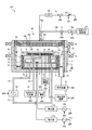
[処理装置100]
図2は、処理装置100の一例を示す断面図である。処理装置100は、例えば図2に示すように、気密に構成された処理チャンバ1を有する。処理チャンバ1は、例えば表面に陽極酸化被膜が施されたアルミニウム等により、略円筒状に形成され、接地されている。処理チャンバ1内には、半導体ウエハWを水平に支持する載置台2が設けられている。
[Processing apparatus 100]
FIG. 2 is a cross-sectional view illustrating an example of the
載置台2は、基材2aおよび静電チャック6を有する。基材2aは、導電性の金属、例えばアルミニウム等で構成されている。載置台2は、下部電極としても機能する。基材2aは、導体の支持台4に支持されている。支持台4は、絶縁板3を介して処理チャンバ1の底部に支持されている。また、載置台2の上方の外周には、例えば単結晶シリコン等で形成されたフォーカスリング5が設けられている。さらに、載置台2および支持台4の周囲を囲むように、例えば石英等からなる円筒状の内壁部材3aが設けられている。
The mounting table 2 includes a
基材2aの上面には、静電チャック6が設けられている。静電チャック6は、半導体ウエハWを吸着保持すると共に、半導体ウエハWを加熱する。静電チャック6は、絶縁体6bと、絶縁体6bの間に設けられた電極6aおよびヒータ6cとを有する。電極6aは、直流電源13に接続されている。静電チャック6は、直流電源13から印加された直流電圧によって静電チャック6の表面にクーロン力を発生させ、発生させたクーロン力により半導体ウエハWを静電チャック6の上面に吸着保持する。直流電源13のオンおよびオフは、後述する制御装置200によって制御される。ヒータ6cは、ヒータ電源30に接続されており、ヒータ電源30から供給された電力に応じて静電チャック6を加熱する。ヒータ電源30からヒータ6cへの電力の供給および停止は、後述する制御装置200によって制御される。また、本実施例において、ヒータ6cへ供給される電力の大きさは、後述する制御装置200からヒータ電源30に指示される。
An
また、静電チャック6は、ヒータ6cからの熱により、半導体ウエハWを加熱する。静電チャック6の上面は、複数の領域である分割領域に分割されており、それぞれの分割領域毎にヒータ6cが設けられている。静電チャック6の上面は、載置台2の載置面に相当する。
The
静電チャック6の下面には、温度センサ20が設けられている。温度センサ20は、温度測定装置14に接続されている。温度センサ20は、分割領域毎に設けられており、分割領域毎の静電チャック6の温度を示す情報を検出し、検出した情報を温度測定装置14へ出力する。温度測定装置14は、温度センサ20から出力された情報に基づいて、分割領域毎の静電チャック6の温度を測定し、測定した温度を制御装置200へ出力する。
A
基材2aの内部には、冷媒が流れる流路2bが形成されている。流路2bには、配管2cおよび2dを介してチラーユニット33が接続されている。チラーユニット33は、配管2cおよび2dを介して、所定の温度に制御されたガルデン等の冷媒を流路2b内に循環させることによって、載置台2を冷却する。チラーユニット33は、後述する制御装置200からの指示に応じて、流路2b内への冷媒の流通の開始および停止を制御する。
A
また、載置台2には、基材2aおよび静電チャック6を貫通するように、半導体ウエハWの裏面側にヘリウムガス等の伝熱ガス(バックサイドガス)を供給するための配管32が設けられている。配管32は、静電チャック6の上面における分割領域毎に設けられ、伝熱ガス供給部31に接続されている。静電チャック6の上面には、それぞれの分割領域内に、伝熱ガスを供給する複数の供給口が設けられている。伝熱ガス供給部31から供給された伝熱ガスは、分割領域毎に、配管32を通って静電チャック6の上面に設けられた複数の供給口から、静電チャック6の上面と半導体ウエハWの裏面との間に供給される。伝熱ガスの圧力は、分割領域毎に独立して制御が可能である。伝熱ガス供給部31から配管32を通って半導体ウエハWの裏面側に供給される伝熱ガスの圧力は、後述する制御装置200によって制御される。なお、静電チャック6の温度は、半導体ウエハWが載置される載置台の温度の一例である。
Further, the mounting table 2 is provided with a
載置台2の上方には、載置台2と略平行に対向するように、換言すれば、載置台2上に載置された半導体ウエハWと対向するように、シャワーヘッド16が設けられている。シャワーヘッド16は、上部電極としても機能する。即ち、シャワーヘッド16と載置台2とは、一対の電極(上部電極と下部電極)として機能する。載置台2の基材2aには、整合器11aを介して高周波電源12aが接続されている。また、載置台2の基材2aには、整合器11bを介して高周波電源12bが接続されている。
Above the mounting table 2, a
高周波電源12aは、プラズマの発生に用いられる所定の周波数(例えば100MHz)の高周波電力を載置台2の基材2aに供給する。また、高周波電源12bは、イオンの引き込み(バイアス)に用いられる所定の周波数の高周波電力であって、高周波電源12aよりも低い周波数(例えば13MHz)の高周波電力を載置台2の基材2aに供給する。高周波電源12aおよび12bのオンおよびオフの制御、ならびに、高周波電源12aおよび12bによって供給される高周波の電力等は、後述する制御装置200によって制御される。
The high
制御装置200は、ヒータ電源30、チラーユニット33、および伝熱ガス供給部31を制御することにより、静電チャック6の上面に吸着保持された半導体ウエハWの温度を、所定の温度に制御することができる。
The
上記したシャワーヘッド16は、処理チャンバ1の上部に設けられている。シャワーヘッド16は、本体部16aと上部天板16bとを備える。シャワーヘッド16は、絶縁性部材45を介して処理チャンバ1の上部に支持されている。本体部16aは、例えば表面が陽極酸化処理されたアルミニウム等により形成され、その下部に上部天板16bを着脱自在に支持する。上部天板16bは、例えば石英等のシリコン含有物質で形成される。
The
本体部16aの内部には、ガス拡散室16cが設けられている。本体部16aの底部には、ガス拡散室16cの下部に位置するように、多数のガス流通口16eが形成されている。上部天板16bには、当該上部天板16bを厚さ方向に貫通するようにガス流通口16fが設けられており、それぞれのガス流通口16fは、上記したガス流通口16eに連通している。このような構成により、ガス拡散室16cに供給された処理ガスは、ガス流通口16eおよびガス流通口16fを介して処理チャンバ1内にシャワー状に拡散されて供給される。なお本体部16a等には、図示しないヒータや、冷媒を循環させるための図示しない配管等の温度調整器が設けられており、半導体ウエハWの処理中にシャワーヘッド16を所望の範囲内の温度に制御できるようになっている。
A
シャワーヘッド16の本体部16aには、ガス拡散室16cに処理ガスを導入するためのガス導入口16gが設けられている。ガス導入口16gには、配管15bの一端が接続されている。配管15bの他端は、弁Vおよびマスフローコントローラ(MFC)15aを介して、半導体ウエハWの処理に用いられる処理ガスを供給する処理ガス供給源15に接続されている。処理ガス供給源15から供給された処理ガスは、配管15bを介してガス拡散室16cに供給され、それぞれのガス流通口16eおよびガス流通口16fを介して処理チャンバ1内にシャワー状に拡散されて供給される。弁VおよびMFC15aは、後述する制御装置200により制御される。
The
上記したシャワーヘッド16には、ローパスフィルタ(LPF)40を介して可変直流電源42が電気的に接続されている。可変直流電源42は、スイッチ41により本体部16aへの直流電力の供給および遮断が可能となっている。可変直流電源42の電流および電圧ならびにスイッチ41のオンおよびオフは、後述する制御装置200によって制御される。例えば、高周波電源12aおよび高周波電源12bから高周波電力が載置台2に供給されて処理チャンバ1内の処理空間にプラズマが生成される際には、必要に応じて制御装置200によりスイッチ41がオンとされ、上部電極として機能するシャワーヘッド16に所定の直流電圧が印加される。
A variable
処理チャンバ1の底部には、排気口71が形成されている。排気口71には、排気管72を介して排気装置73が接続されている。排気装置73は、真空ポンプを有しており、この真空ポンプを作動させることにより処理チャンバ1内を所定の真空度まで減圧することができる。排気装置73による排気量等は、後述する制御装置200により制御される。また、処理チャンバ1の側壁には、開口部74が設けられており、開口部74には、当該開口部74を開閉するゲートバルブGが設けられている。
An exhaust port 71 is formed at the bottom of the
処理チャンバ1の内壁には、内壁の面に沿って、デポシールド76が、着脱自在に設けられている。また、載置台2、内壁部材3a、および支持台4の外周面には、載置台2、内壁部材3a、および支持台4の外周面に沿ってデポシールド77が設けられている。デポシールド76および77は、処理チャンバ1の内壁にエッチング副生物(デポ)が付着することを防止する。静電チャック6上に吸着保持された半導体ウエハWと略同じ高さのデポシールド76の位置には、直流的にグランドに接続された導電性部材(GNDブロック)79が設けられている。導電性部材79により、処理チャンバ1内の異常放電が抑制される。
A
また、処理チャンバ1の周囲には、同心円状にリング磁石8が配置されている。リング磁石8は、シャワーヘッド16と載置台2との間の空間に磁場を形成する。リング磁石8は、図示しない回転機構により回転自在に保持されている。
A
[静電チャック6]
図3は、静電チャック6の上面の一例を示す図である。図4は、図3のA−A断面の一例を示す図である。静電チャック6の外周には、静電チャック6を囲むようにフォーカスリング5が設けられている。半導体ウエハWが載置される静電チャック6の上面は、例えば同心円状に複数の分割領域に分けられている。本実施例において、静電チャック6の上面は、例えば2つの分割領域60aおよび60bに分けられている。なお、以下では、分割領域60aをセンタ領域、分割領域60bをエッヂ領域と呼ぶ場合がある。また、以下では、複数の分割領域60aおよび60bのそれぞれを区別することなく総称する場合に分割領域60と記載する。
[Electrostatic chuck 6]
FIG. 3 is a diagram illustrating an example of the upper surface of the
例えば図4に示すように、静電チャック6の内部であって、それぞれの分割領域60の下方には、分割領域60毎にヒータ6cが設けられている。なお、ヒータ6cは、静電チャック6の外部に設けられていてもよい。制御装置200は、ヒータ電源30からそれぞれのヒータ6cに供給される電力を制御することにより、それぞれの分割領域60の温度を独立に制御することができる。
For example, as shown in FIG. 4, a
例えば図4に示すように、静電チャック6の下面には、分割領域60毎に温度センサ20が少なくとも1つ設けられている。本実施例において、温度センサ20は、例えば図3に示すように、分割領域60a内の領域21a、および、分割領域60b内の領域21bに、それぞれ1つずつ設けられている。
For example, as shown in FIG. 4, at least one
温度センサ20は、例えば図4に示すように、感温体22および読取部23を有する。感温体22は、温度に応じて特性が変化する。本実施例において、感温体22は、蛍光体であり、静電チャック6の温度に応じて、蛍光特性が変化する。読取部23は、温度に応じて変化した感温体22の特性を読み取って温度測定装置14へ出力する。本実施例において、読取部23は、例えば光ファイバであり、温度測定装置14から出力されたパルス光を感温体22に照射し、照射されたパルス光に応じて感温体22が発した光を温度測定装置14へ伝送する。
For example, as shown in FIG. 4, the
温度測定装置14は、分割領域60毎に、分割領域60に設けられた温度センサ20から出力された信号に基づいて、分割領域60の温度を測定し、測定した分割領域60毎の温度の情報を制御装置200へ出力する。温度測定装置14は、例えば読取部23を介して感温体22へパルス光を送信し、読取部23を介して受信した感温体22の光の減衰速度に基づいて、感温体22が設けられた分割領域60の温度を測定する。
The
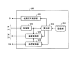
[制御装置200]
図5は、制御装置200の一例を示すブロック図である。制御装置200は、例えば図5に示すように、伝熱ガス制御部201、取得部202、算出部203、記憶部204、温度制御部205、および処理制御部206を有する。
[Control device 200]
FIG. 5 is a block diagram illustrating an example of the
記憶部204は、例えば図6に示すような補正テーブル2040を記憶する。図6は、実施例1における補正テーブル2040の一例を示す図である。補正テーブル2040には、分割領域60毎に個別テーブル2041が格納される。それぞれの個別テーブル2041には、静電チャック6の温度変化の傾きに対応付けて、静電チャック6の温度を所定の温度に制御する際に適用される補正値が格納される。
The
図5に戻って説明を続ける。伝熱ガス制御部201は、算出部203からの指示に応じて、伝熱ガス供給部31に伝熱ガスの供給開始および供給停止を指示する。また、伝熱ガス制御部201は、算出部203からの指示に応じて、伝熱ガスの圧力を伝熱ガス供給部31に指示する。
Returning to FIG. The heat transfer
取得部202は、温度測定装置14から、分割領域60毎に測定された温度の情報を取得する。そして、取得部202は、分割領域60毎に、取得した温度の情報を算出部203および温度制御部205へ出力する。また、取得部202は、補正テーブル2040の作成時に、処理装置100の処理チャンバ1内に搬入された温度測定用ウエハW’から出力された温度の情報を取得し、取得した温度の情報を、算出部203へ出力する。
The
温度測定用ウエハW’は、温度測定用ウエハW’の表面に設けられた複数の温度センサと、それぞれの温度センサによって測定された温度の情報を制御装置200へ出力する通信部とを有する。それぞれの温度センサは、静電チャック6上に載置された場合に、静電チャック6の分割領域60に対応する温度測定用ウエハW’上の領域に少なくとも1つ設けられる。通信部は、それぞれの温度センサによって分割領域60毎に測定された温度の情報を、無線通信により制御装置200へ送信する。なお、通信部は、分割領域60毎の温度の情報を、有線通信により制御装置200へ送信してもよい。また、温度測定用ウエハW’は、通信部に代えて不揮発性の記憶装置を有し、それぞれの温度センサによって分割領域60毎に測定された温度の情報を記憶装置に記憶させてもよい。この場合、処理チャンバ1から温度測定用ウエハW’が搬出された後に、制御装置200の取得部202が、それぞれの温度センサによって分割領域60毎に測定された温度の情報を記憶装置から読み出す。
The temperature measurement wafer W ′ includes a plurality of temperature sensors provided on the surface of the temperature measurement wafer W ′, and a communication unit that outputs information on the temperature measured by each temperature sensor to the
温度制御部205は、算出部203からの指示に応じて、ヒータ電源30およびチラーユニット33を制御する。温度制御部205は、静電チャック6の冷却開始を算出部203から指示された場合に、基材2aの流路2b内に所定温度の冷媒を循環させるようにチラーユニット33に指示する。また、温度制御部205は、静電チャック6内のヒータ6cへの電力供給の停止あるいはヒータ6cへ供給される電力の固定を算出部203から指示された場合に、ヒータ6cへの電力供給の停止あるいはヒータ6cへ供給される電力の固定をヒータ電源30に指示する。
The
また、温度制御部205は、補正テーブル2040の作成時に、処理制御部206から目標温度を受け付ける。そして、算出部203からヒータ6cへの電力供給の開始を指示された場合、温度制御部205は、ヒータ6cへの電力供給の開始をヒータ電源30に指示する。そして、温度制御部205は、取得部202から出力された分割領域60毎の温度情報に基づいて、分割領域60の温度が目標温度となるように、分割領域60毎に設けられたヒータ6cに供給される電力をフィードバック制御する。
Further, the
また、温度制御部205は、半導体ウエハWに対する処理の実行に、算出部203から分割領域60毎の補正値を受け付け、処理制御部206から目標温度を受け付ける。そして、算出部203からヒータ6cへの電力供給の開始を指示された場合、温度制御部205は、ヒータ6cへの電力供給の開始をヒータ電源30に指示する。そして、温度制御部205は、分割領域60毎に、補正値に基づいて目標温度を補正する。そして、温度制御部205は、取得部202から出力された分割領域60毎の温度情報に基づいて、分割領域60毎に、分割領域60の温度が補正後の目標温度となるように、ヒータ6cに供給される電力をフィードバック制御する。これにより、静電チャック6上に載置された半導体ウエハWの温度が、補正後の目標温度に、半導体ウエハWと静電チャック6との間の熱抵抗によって半導体ウエハWと静電チャック6との間に生じた温度差を加えた温度となるように制御される。算出部203は、半導体ウエハWと静電チャック6との間の熱抵抗が大きい場合に、目標温度が低くなるように目標温度を補正し、半導体ウエハWと静電チャック6との間の熱抵抗が小さい場合に、目標温度が高くなるように目標温度を補正する。これにより、温度制御部205は、半導体ウエハWと静電チャック6との間の熱抵抗が変化した場合でも、複数の半導体ウエハW間の温度のばらつきを抑制することができる。
Further, the
処理制御部206は、補正テーブル2040の作成時に、算出部203からの指示に応じて、補正テーブル2040の作成時の目標温度を温度制御部205へ出力する。そして、処理制御部206は、算出部203からの指示に応じて、処理装置100の各部を制御する。また、処理制御部206は、半導体ウエハWに対する処理の実行時に、処理装置100のオペレータ等により設定された処理レシピにおいて指定された目標温度を温度制御部205へ出力する。そして、処理制御部206は、処理レシピに基づいて、処理装置100の各部を制御することにより、半導体ウエハWに対する処理を実行する。
When the correction table 2040 is created, the
算出部203は、補正テーブル2040の作成時および半導体ウエハWに対する処理の実行時に、伝熱ガス制御部201、温度制御部205、および処理制御部206をそれぞれ制御する。以下、図7および図8を参照しながら、算出部203によって行われる処理の詳細について説明する。
The
[補正テーブル2040の作成処理]
図7は、補正テーブル2040の作成時における温度測定用ウエハW’および静電チャック6の温度変化の一例を示す図である。図7は、静電チャック6上の一つの分割領域(例えばセンタ領域)に対応する領域の温度測定用ウエハW’および静電チャック6の温度変化の一例を示している。また、以下では、補正テーブル2040のうち、一つの分割領域60における個別テーブル2041の作成処理について説明する。なお、他の分割領域60における個別テーブル2041の作成処理についても同様であるため、他の分割領域60における個別テーブル2041の作成処理については説明を省略する。
[Creation process of correction table 2040]
FIG. 7 is a diagram illustrating an example of temperature changes of the temperature measurement wafer W ′ and the
図7(a)は伝熱ガスの圧力が5Torrの場合、図7(b)は伝熱ガスの圧力が10Torrの場合、図7(c)は伝熱ガスの圧力が20Torrの場合の温度測定用ウエハW’および静電チャックの温度変化の一例をそれぞれ示している。図7において、グラフ80は温度測定用ウエハW’の温度変化を示し、グラフ81は静電チャック6の温度変化を示している。
FIG. 7A shows the temperature measurement when the heat transfer gas pressure is 5 Torr, FIG. 7B shows the temperature measurement when the heat transfer gas pressure is 10 Torr, and FIG. 7C shows the temperature measurement when the heat transfer gas pressure is 20 Torr. An example of temperature changes of the wafer W ′ and the electrostatic chuck is shown. In FIG. 7, a
補正テーブル2040の作成時において、算出部203は、まず、静電チャック6の冷却開始と、ヒータ6cへの電力供給の停止あるいはヒータ6cへ供給される電力の固定とを温度制御部205に指示する。これにより、静電チャック6は、基材2aの流路2b内を循環する冷媒により冷却された基材2aを介して冷却される。そして、算出部203は、図示しない搬送ロボットに指示して、温度測定用ウエハW’を処理チャンバ1内に搬入させ、静電チャック6上に載置させる。
When creating the correction table 2040, the
なお、例えば図7に示すように、温度測定用ウエハW’が静電チャック6上に載置された時点t0では、半導体ウエハWの温度は室温(例えば30℃)であり、静電チャック6の温度は室温より低い温度(例えば10℃)に冷却されている。つまり、温度測定用ウエハW’が静電チャック6上に載置された段階では、温度測定用ウエハW’と静電チャック6とは異なる温度である。
For example, as shown in FIG. 7, at the time t 0 when the temperature measuring wafer W ′ is placed on the
次に、算出部203は、取得部202を介して分割領域60毎の静電チャック6の温度情報の取得を開始することにより、分割領域60毎に、温度測定用ウエハW’および静電チャック6の温度測定を開始する。そして、算出部203は、図7に示した時点t1において、所定圧力の伝熱ガスの供給開始を伝熱ガス制御部201に指示する。本実施例において、算出部203は、伝熱ガスの圧力として、5Torr、10Torr、および20Torrのいずれかを伝熱ガス制御部201に指示する。伝熱ガス制御部201は、分割領域60毎に、算出部203から指示された圧力の伝熱ガスの供給を伝熱ガス供給部31に指示する。これにより、時点t1において、分割領域60毎に、静電チャック6の上面と温度測定用ウエハW’の裏面との間に伝熱ガスが供給され、温度測定用ウエハW’と静電チャック6との間で、伝熱ガスを介した熱交換が始まる。そして、例えば図7に示すように、温度測定用ウエハW’との熱交換により、温度測定用ウエハW’の温度が下がり、静電チャック6の温度が上がる。
Next, the
そして、時点t1から所定時間(例えば十秒程度)が経過した後の時点t2において、算出部203は、ヒータ6cへの電力供給の開始を温度制御部205に指示する。温度制御部205は、ヒータ電源30にヒータ6cへの電力供給の開始を指示し、分割領域60毎に、分割領域60の温度が目標温度(例えば60℃)となるように、ヒータ6cに供給される電力のフィードバック制御を開始する。これにより、例えば図7に示すように、分割領域60毎に、静電チャック6の温度と温度測定用ウエハW’の温度とが、目標温度に徐々に近づく。
Then, at time t 2 after the time t 1 a predetermined time (for example, about ten seconds) has elapsed, the calculating
次に、静電チャック6および温度測定用ウエハW’の温度が安定した時点t3において、処理制御部206は、補正テーブル2040の作成時の処理レシピに基づいて、高周波電力や処理ガスの供給等の制御を開始する。例えば、処理制御部206は、高周波電力の供給開始を高周波電源12aおよび高周波電源12bにそれぞれ指示すると共に、所定の流量の処理ガスが処理チャンバ1内に供給されるように弁VおよびMFC15aを制御する。これにより、処理装置100の処理チャンバ1内には、処理ガスのプラズマが生成される。そして、処理チャンバ1内に生成されたプラズマからの入熱により、例えば図7に示すように、温度測定用ウエハW’の温度が上昇する。プラズマからの入熱は、静電チャック6に伝わり、静電チャック6から放熱される。しかし、半導体ウエハWと静電チャック6との間には、熱抵抗が存在する。そのため、半導体ウエハWと静電チャック6との間には、半導体ウエハWと静電チャック6との間の熱抵抗に応じた温度差が生じる。
Next, at the time point t 3 when the temperature of the
伝熱ガスの圧力が5Torrである図7(a)の例では、プラズマからの入熱により、温度測定用ウエハW’の温度が例えばTa=74.4℃まで上昇する。静電チャック6は温度制御部205によってほぼ60℃に制御されているので、プラズマからの入熱により温度が上昇した温度測定用ウエハW’と、静電チャック6との間の温度差ΔTaは14.4℃である。また、伝熱ガスの圧力が10Torrである図7(b)の例では、プラズマからの入熱により、温度測定用ウエハW’の温度が例えばTb=69.9℃まで上昇する。プラズマからの入熱により温度が上昇した温度測定用ウエハW’と、静電チャック6との間の温度差ΔTbは9.9℃である。また、伝熱ガスの圧力が20Torrである図7(c)の例では、プラズマからの入熱により、温度測定用ウエハW’の温度が例えばTc=66.6℃まで上昇する。プラズマからの入熱により温度が上昇した温度測定用ウエハW’と、静電チャック6との間の温度差ΔTcは6.6℃である。
The pressure of the heat transfer gas in the example of FIG. 7 (a) is 5 Torr, the heat input from the plasma, rises to a temperature, for example T a = 74.4 ° C. of the temperature measurement for the wafer W '. Since the
なお、時点t3において、処理チャンバ1内に供給される高周波電力の周波数や電力、処理ガスの種類や流量等は、半導体ウエハWに対して行われる処理のレシピで指定されている高周波電力の周波数や電力、処理ガスの種類や流量等が用いられることが好ましい。これにより、半導体ウエハWに対して実際に行われる処理環境における半導体ウエハWの温度を測定することができる。
At time t 3 , the frequency and power of the high-frequency power supplied into the
そして、算出部203は、処理レシピの実行停止を処理制御部206に指示する。これにより、処理チャンバ1内でのプラズマの生成が停止される。そして、算出部203は、ヒータ6cへの電力供給の停止あるいはヒータ6cへ供給される電力の固定を温度制御部205に指示し、伝熱ガスの供給停止を伝熱ガス制御部201に指示する。これにより、静電チャック6上に載置された温度測定用ウエハW’の温度が徐々に室温(例えば30℃)に戻り、静電チャック6の温度がチラーユニット33によって徐々に室温より低い温度(例えば10℃)に戻る。
Then, the
算出部203は、所定数の圧力の伝熱ガスのそれぞれについて、分割領域毎に上記の処理を行うことにより、温度測定用ウエハW’および静電チャック6の温度変化を測定する。そして、算出部203は、それぞれの圧力の伝熱ガスについて、温度変化の測定データから、分割領域毎に、時点t1と時点t2との間の静電チャック6の温度変化の傾きを算出する。ここで、静電チャック6の温度変化の傾きの算出方法について、図8を用いて説明する。
The
図8は、補正テーブル作成時における温度測定用ウエハW’および静電チャック6の温度変化の一例を示す拡大図である。図8は、静電チャック6上の一つの分割領域(例えばセンタ領域)に対応する領域の温度測定用ウエハW’および静電チャック6の温度変化の一例を示している。また、図8(a)は図7(a)における時点t1付近の拡大図であり、図8(b)は図7(b)における時点t1付近の拡大図であり、図8(c)は図7(c)における時点t1付近の拡大図である。
FIG. 8 is an enlarged view showing an example of temperature changes of the temperature measuring wafer W ′ and the
算出部203は、例えば図8に示すように、伝熱ガスの供給が開始された時点t1より第1の時間が経過した時点t11と、時点t11から第2の時間Δtが経過した時点t12との間の期間の静電チャック6の温度変化の傾きを測定する。本実施例において、第1の時間は例えば1秒であり、第2の時間Δtは例えば5秒である。図8(a)〜(c)に示すように、時点t11から時点t12までの間の静電チャック6の温度変化の傾きは、伝熱ガスの圧力に応じて変化している。これは、伝熱ガスの圧力に応じて、温度測定用ウエハW’と静電チャック6との間の熱抵抗が変化するためである。
For example, as shown in FIG. 8, the
そして、算出部203は、それぞれの圧力の伝熱ガスについて、温度変化の測定データから、分割領域毎に、プラズマ生成中の温度測定用ウエハW’の温度(例えば図7に示したTa、Tb、およびTc)を取得する。図9は、伝熱ガスの圧力毎の静電チャック6の温度変化の傾きおよび温度測定用ウエハW’の温度のデータ62の一例を示す図である。算出部203は、例えば図9のデータ62に示すように、各分割領域について、伝熱ガスの圧力毎に、静電チャック6の温度変化の傾きを算出すると共に、プラズマ生成中の温度測定用ウエハW’の温度を取得する。そして、算出部203は、例えば下記の算出式(1)に基づいて、各分割領域について、伝熱ガスの圧力毎に、補正値Toffを算出する。
Toff=Tr−Tm ・・・(1)
ここで、Tmは、プラズマ生成中の温度測定用ウエハW’の温度を示し、Trは、基準となる温度を示す。
Then, calculating
T off = T r −T m (1)
Here, T m represents the temperature of the temperature measuring wafer W ′ during plasma generation, and T r represents a reference temperature.
本実施例では、一例として、伝熱ガスの圧力が10Torrの場合の温度測定用ウエハW’の温度Tmが基準となる温度Trとして設定される。そのため、図9に例示したデータ62において、センタ領域では、基準となる温度Trが69.9℃、エッジ領域では基準となる温度Trが72.2℃となる。例えば図9のデータ62において、伝熱ガスの圧力が5Torrの場合、センタ領域の温度測定用ウエハW’の温度Tmが74.4℃なので、算出部203は、69.9−74.4=−4.5を、伝熱ガスの圧力が5Torrの場合のセンタ領域の補正値Toffとして算出する。同様に、例えば図9のデータ62において、伝熱ガスの圧力が20Torrの場合、センタ領域の温度測定用ウエハW’の温度Tmが66.6℃なので、算出部203は、69.9−66.6=+3.3を、伝熱ガスの圧力が20Torrの場合のセンタ領域の補正値Toffとして算出する。
In this embodiment, as an example, the temperature T m of the temperature measuring wafer W ′ when the pressure of the heat transfer gas is 10 Torr is set as the reference temperature T r . Therefore, in the
算出部203は、伝熱ガスの圧力毎に静電チャック6の温度変化の傾きと補正値Toffとを対応付けた個別テーブル2041(図6参照)を、分割領域毎に作成し、作成した個別テーブル2041を含む補正テーブル2040を、記憶部204に保存する。
ここで、温度測定用ウエハW’と静電チャック6との間の熱抵抗は、所定の温度差を有する温度測定用ウエハW’と静電チャック6とが熱交換を行った場合の温度測定用ウエハW’および静電チャック6のそれぞれの温度変化の傾きから推定することができる。例えば、温度測定用ウエハW’と静電チャック6との間の熱抵抗が小さい場合には、静電チャック6の温度変化の傾きが大きくなり、温度測定用ウエハW’と静電チャック6との間の熱抵抗が大きい場合には、静電チャック6の温度変化の傾きが小さくなる。また、温度測定用ウエハW’と静電チャック6との間の熱抵抗が大きい場合、プラズマ生成中の温度測定用ウエハW’と静電チャック6との間の温度差が大きくなり、温度測定用ウエハW’と静電チャック6との間の熱抵抗が小さい場合、プラズマ生成中の温度測定用ウエハW’と静電チャック6との間の温度差が小さくなる。
Here, the thermal resistance between the temperature measurement wafer W ′ and the
そのため、本実施例では、温度測定用ウエハW’と静電チャック6との間の熱抵抗が大きい場合、即ち、静電チャック6の温度変化の傾きが小さい場合に、静電チャック6の目標温度を下げるような補正値を算出する。一方、温度測定用ウエハW’と静電チャック6との間の熱抵抗が小さい場合、即ち、静電チャック6の温度変化の傾きが大きい場合に、静電チャック6の目標温度を上げるような補正値を算出する。そして、プラズマ生成中に測定された温度測定用ウエハW’の温度と、基準温度との差が、補正値の大きさに設定される。半導体ウエハWの処理時には、半導体ウエハWを載置した静電チャック6の温度変化が測定され、静電チャック6の温度変化の傾きに対応する補正値が、半導体ウエハWに対するプラズマ処理が行われる際の静電チャック6の目標温度に適用される。これにより、半導体ウエハWと静電チャック6との間の熱抵抗の変化に伴って、プラズマ処理時の半導体ウエハWの温度が半導体ウエハW間で変動することが抑制される。
Therefore, in this embodiment, when the thermal resistance between the temperature measurement wafer W ′ and the
[半導体ウエハWの処理時の補正]
図10は、補正値が適用された場合の温度測定用ウエハW’および静電チャック6の温度変化の一例を示す図である。図10は、静電チャック6上の一つの分割領域(例えばセンタ領域)における温度測定用ウエハW’および静電チャック6の温度変化の一例を示している。また、図10(a)は伝熱ガスの圧力が5Torrの場合、図10(b)は伝熱ガスの圧力が10Torrの場合、図10(c)は伝熱ガスの圧力が20Torrの場合の温度測定用ウエハW’および静電チャックの温度変化の一例をそれぞれ示している。図10において、グラフ80は温度測定用ウエハW’の温度変化を示し、グラフ81は静電チャック6の温度変化を示している。
[Correction during processing of semiconductor wafer W]
FIG. 10 is a diagram illustrating an example of a temperature change of the temperature measurement wafer W ′ and the
ここで、処理装置100が処理した半導体ウエハWの数が多くなるほど、即ち、処理装置100において実行された処理の累積時間が長くなるほど、処理チャンバ1内の環境の変化により半導体ウエハWと静電チャック6との間の熱抵抗の変化が大きくなる。例えば、複数の半導体ウエハWに対して所定の膜を積層させる処理が行われる場合、処理の累積時間が長くなるほど、デポの付着量の増加により半導体ウエハWと静電チャック6との間の熱抵抗が低くなる。半導体ウエハWと静電チャック6との間の熱抵抗は、半導体ウエハWと静電チャック6との間に供給される伝熱ガスの圧力で制御することができる。そのため、図10では、半導体ウエハWと静電チャック6との間の熱抵抗の変化を、伝熱ガスの圧力の変化で模擬している。
Here, as the number of the semiconductor wafers W processed by the
伝熱ガスの圧力が5Torr(図10(a))の場合の半導体ウエハWと静電チャック6との間の熱抵抗は、半導体ウエハWに対する処理の累積時間が例えば0時間、即ち、新品の状態の静電チャック6と半導体ウエハWとの間の熱抵抗に相当する。また、伝熱ガスの圧力が10Torr(図10(b))の場合の半導体ウエハWと静電チャック6との間の熱抵抗は、処理の累積時間が例えば30時間の静電チャック6と半導体ウエハWとの間の熱抵抗に相当する。また、伝熱ガスの圧力が20Torr(図10(c))の場合の半導体ウエハWと静電チャック6との間の熱抵抗は、処理の累積時間が例えば60時間の静電チャック6と半導体ウエハWとの間の熱抵抗に相当する。なお、図10では、ウエハの温度をモニタするために温度測定用ウエハW’が用いられているが、図10に示した温度変化は、半導体ウエハWに対する処理の実行時も同様である。そのため、以下の説明では、半導体ウエハWに対する処理として説明する。
The thermal resistance between the semiconductor wafer W and the
半導体ウエハWに対する処理の実行時において、算出部203は、まず、静電チャック6の冷却開始と、ヒータ6cへの電力供給の停止あるいはヒータ6cへ供給される電力の固定とを温度制御部205に指示する。これにより、静電チャック6は、基材2aの流路2b内を循環する冷媒により冷却された基材2aを介して冷却される。また、算出部203は、半導体ウエハWに対する処理に用いられる処理レシピの実行を処理制御部206に指示する。処理制御部206は、処理レシピに基づいて、半導体ウエハWに対する処理を行う際の静電チャック6の目標温度を温度制御部205に指示する。そして、算出部203は、図示しない搬送ロボットに指示して、半導体ウエハWを処理チャンバ1内に搬入させ、静電チャック6上に載置させる。なお、半導体ウエハWが静電チャック6上に載置された時点t0では、半導体ウエハWは室温(例えば30℃)であり、静電チャック6は室温より低い温度(例えば10℃)に冷却されている。
When executing processing on the semiconductor wafer W, the
次に、算出部203は、取得部202を介して分割領域60毎の静電チャック6の温度情報の取得を開始することにより、分割領域60毎に静電チャック6の温度測定を開始する。そして、算出部203は、図10に示した時点t1において、半導体ウエハWの処理レシピで指定された圧力の伝熱ガスの供給開始を伝熱ガス制御部201に指示する。これにより、時点t1において、分割領域60毎に、静電チャック6の上面と半導体ウエハWの裏面との間に伝熱ガスが供給され、半導体ウエハWと静電チャック6との間で、伝熱ガスを介した熱交換が始まる。これにより、例えば図10に示すように、半導体ウエハWとの熱交換により、半導体ウエハWの温度が下がり、静電チャック6の温度が上がる。
Next, the
そして、算出部203は、伝熱ガスの供給を開始した時点t1から第1の時間が経過した時点t11と、時点t11から第2の時間が経過した時点t12との間の期間の静電チャック6の温度変化の傾きを、分割領域60毎に測定する。そして、算出部203は、分割領域60毎に記憶部204内の個別テーブル2041を参照し、測定した静電チャック6の温度変化の傾きに対応する補正値を取得する。本実施例において、算出部203は、分割領域60毎に、例えば、測定した静電チャック6の温度変化の傾きに最も近い傾きを個別テーブル2041内で特定し、特定した傾きに対応付けられている補正値を取得する。また、他の例として、算出部203は、個別テーブル2041内の傾きと補正値との関係を近似するフィッティングカーブを求め、測定した静電チャック6の温度変化の傾きに対応するフィッティングカーブ上の補正値を取得するようにしてもよい。
Then, calculating
そして、算出部203は、分割領域60毎に取得した補正値を温度制御部205へ出力する。そして、算出部203は、時点t1から所定時間が経過した後の時点t2において、ヒータ6cへの電力供給の開始を温度制御部205に指示する。温度制御部205は、分割領域60毎に、処理制御部206から指示された目標温度に、算出部203から指示された補正値を加えることにより、目標温度を補正する。そして、温度制御部205は、分割領域60毎に、静電チャック6の温度が補正後の目標温度となるようにヒータ6cの電力をフィードバック制御する。これにより、静電チャック6は、伝熱ガスの供給が開始された時点t1から、ヒータ6cへの電力供給が開始される時点t2までの間の静電チャック6の温度変化に応じた補正値が適用された目標温度に制御される。なお、温度制御部205は、分割領域60毎の補正値が算出部203から出力された場合に、時点t2まで待つことなく、算出部203から指示された補正値で補正した目標温度となるように、ヒータ6cの電力のフィードバック制御を開始してもよい。
Then, the
そして、静電チャック6と半導体ウエハWの温度が安定した時点t3において、処理制御部206は、半導体ウエハWに対する処理に用いられる処理レシピに従って、高周波電力および処理ガスの供給等の制御を開始する。これにより、処理チャンバ1内に処理ガスのプラズマが生成され、プラズマにより半導体ウエハWに対して所定の処理が実行される。そして、プラズマからの入熱により、半導体ウエハWの温度が上昇する。
Then, at the time t 3 when the temperature of the
ここで、伝熱ガスの圧力が5Torrである図10(a)の例では、ヒータ6cへの電力供給の開始前のセンタ領域の静電チャック6の温度変化の傾きが0.23である。そのため、図6に示した補正テーブル2040が記憶部204に保存されている場合、算出部203は、例えば−4.5を補正値として取得する。そして、温度制御部205は、目標温度が60℃である場合、55.5℃を補正後の目標温度として算出し、静電チャック6のセンタ領域の温度が55.5℃になるようにヒータ6cの電力をフィードバック制御する。図7(a)において説明したように、伝熱ガスの圧力が5Torrの場合の半導体ウエハWと静電チャック6との間の温度差ΔTaは14.4℃であるため、プラズマ処理時の半導体ウエハWの温度Ta’は約70℃に制御される。
Here, in the example of FIG. 10A in which the pressure of the heat transfer gas is 5 Torr, the gradient of the temperature change of the
また、伝熱ガスの圧力が10Torrである図10(b)の例では、ヒータ6cへの電力供給の開始前のセンタ領域の静電チャック6の温度変化の傾きが0.33である。そのため、図6に示した補正テーブル2040が記憶部204に保存されている場合、算出部203は、例えば0を補正値として取得する。そして、温度制御部205は、目標温度が60℃である場合、60℃を補正後の目標温度として算出し、静電チャック6のセンタ領域の温度が60℃になるようにヒータ6cの電力をフィードバック制御する。図7(b)において説明したように、伝熱ガスの圧力が10Torrの場合の半導体ウエハWと静電チャック6との間の温度差ΔTbは9.9℃であるため、プラズマ処理時の半導体ウエハWの温度Tb’は約70℃に制御される。
Further, in the example of FIG. 10B in which the pressure of the heat transfer gas is 10 Torr, the gradient of the temperature change of the
また、伝熱ガスの圧力が20Torrである図10(c)の例では、ヒータ6cへの電力供給の開始前のセンタ領域の静電チャック6の温度変化の傾きが0.42である。そのため、図6に示した補正テーブル2040が記憶部204に保存されている場合、算出部203は、例えば+3.3を補正値として取得する。そして、温度制御部205は、目標温度が60℃である場合、63.3℃を補正後の目標温度として算出し、静電チャック6のセンタ領域の温度が63.3℃になるようにヒータ6cの電力をフィードバック制御する。図7(c)において説明したように、伝熱ガスの圧力が20Torrの場合の半導体ウエハWと静電チャック6との間の温度差ΔTcは6.6℃であるため、プラズマ処理時の半導体ウエハWの温度Tc’は約70℃に制御される。
In the example of FIG. 10C in which the pressure of the heat transfer gas is 20 Torr, the gradient of the temperature change of the
このように、温度センサ20は、半導体ウエハWと静電チャック6との間の熱抵抗が大きい場合、即ち、静電チャック6の温度変化の傾きが小さい場合に、静電チャック6の目標温度を下げ、半導体ウエハWと静電チャック6との間の熱抵抗が小さい場合、即ち、静電チャック6の温度変化の傾きが大きい場合に、静電チャック6の目標温度を上げるようにヒータ6cに供給される電力をフィードバック制御する。これにより、複数の半導体ウエハWが処理される過程で半導体ウエハWと静電チャック6との間の熱抵抗が変化した場合であっても、複数の半導体ウエハW間で、プラズマ処理時の温度のばらつきを抑制することができる。
As described above, the
[補正テーブル2040作成時の処理フロー]
図11は、実施例1における補正テーブル作成処理の一例を示すフローチャートである。なお、図11に示した処理に先立って、ヒータ電源30は、ヒータ6cへの電力供給を停止あるいは固定しており、静電チャック6は、基材2a内を流通する冷媒により所定温度まで冷却されている。また、温度測定用ウエハW’の温度は室温である。
[Processing flow when creating correction table 2040]
FIG. 11 is a flowchart illustrating an example of a correction table creation process according to the first embodiment. Prior to the processing shown in FIG. 11, the
まず、算出部203は、図示しない搬送ロボットに指示して、温度測定用ウエハW’を処理チャンバ1内に搬入させ、静電チャック6上に載置させる(S100)。そして、算出部203は、温度測定用ウエハW’と静電チャック6との間に供給される伝熱ガスの圧力を分割領域60毎に選択する(S101)。本実施例において、算出部203は、伝熱ガスの圧力として、5Torr、10Torr、および20Torrのいずれか一つを順次選択する。
First, the
次に、算出部203は、取得部202を介して分割領域60毎の静電チャック6の温度情報の取得を開始する(S102)。そして、算出部203は、ステップS101で分割領域60毎に選択した圧力における伝熱ガスの供給開始を伝熱ガス制御部201に指示する。これにより、分割領域60毎に、温度測定用ウエハW’と静電チャック6との間への伝熱ガスの供給が開始される(S103)。そして、温度測定用ウエハW’と静電チャック6との間で、伝熱ガスを介した熱交換が始まる。
Next, the
次に、算出部203は、伝熱ガスの供給開始から所定時間(例えば十秒程度)が経過するまで待機する(S104)。そして、算出部203は、ヒータ6cへの電力供給の開始を温度制御部205に指示する。これにより、ヒータ電源30からヒータ6cへの電力供給が開始される(S105)。そして、温度制御部205は、静電チャック6の温度が目標温度となるように、ヒータ6cに供給される電力のフィードバック制御を開始する。
Next, the
次に、処理制御部206は、温度測定用ウエハW’の温度が安定するまで所定時間待機する(S106)。そして、処理制御部206は、補正テーブル2040作成時の処理レシピに基づいて、高周波電力や処理ガスの供給等の制御を開始することにより、処理チャンバ1内に処理ガスのプラズマを生成する(S107)。
Next, the
次に、処理制御部206は、温度測定用ウエハW’の温度が安定するまで所定時間待機する(S108)。そして、処理制御部206は、高周波電力や処理ガスの供給等を停止する(S109)。そして、算出部203は、伝熱ガスの供給停止を伝熱ガス制御部201に指示し、ヒータ6cへの電力供給の停止あるいはヒータ6cへ供給される電力の固定を温度制御部205に指示する(S110)。そして、算出部203は、分割領域60毎の静電チャック6の温度情報の取得を停止する(S111)。
Next, the
次に、算出部203は、測定対象の全ての圧力(本実施例では、5Torr、10Torr、および20Torr)について、温度測定用ウエハW’および静電チャック6の温度測定を行ったか否かを判定する(S112)。測定対象の圧力の中に、温度測定用ウエハW’および静電チャック6の温度測定が行われていない圧力がある場合(S112:No)、算出部203は、チラーユニット33によって静電チャック6が所定温度まで冷却され、かつ、温度測定用ウエハW’の温度が室温に戻るまで、所定時間待機する(S113)。そして、算出部203は、再びステップS101に示した処理を実行する。
Next, the
一方、測定対象の全ての圧力について、温度測定用ウエハW’および静電チャック6の温度測定を行った場合(S112:Yes)、算出部203は、図8を用いて説明したように、各分割領域60について、伝熱ガスの圧力毎に、伝熱ガスの供給が開始された時点t1から第1の時間が経過した時点t11と、時点t11から第2の時間Δtが経過した時点t12との間の期間の静電チャック6の温度変化の傾きを算出する(S114)。
On the other hand, when the temperature of the temperature measurement wafer W ′ and the
次に、算出部203は、各分割領域60について、伝熱ガスの圧力毎に、前述の算出式(1)に基づいて、基準となる温度に対する補正値Toffを算出する(S115)。そして、算出部203は、各分割領域60について、伝熱ガスの圧力毎に、静電チャック6の温度変化の傾きと補正値Toffとを対応付けた個別テーブル2041(図6参照)を作成し、作成した個別テーブル2041を含む補正テーブル2040を記憶部204に保存する(S116)。
Next, the
[半導体ウエハWに対する処理の実行時の処理フロー]
図12は、実施例1における半導体ウエハWに対する処理の一例を示すフローチャートである。なお、図12に示した処理に先立って、ヒータ電源30は、ヒータ6cへの電力供給を停止あるいは固定しており、静電チャック6は、基材2a内を流通する冷媒により所定温度まで冷却されている。また、半導体ウエハWの温度は室温である。
[Processing flow when executing processing on semiconductor wafer W]
FIG. 12 is a flowchart illustrating an example of processing for the semiconductor wafer W in the first embodiment. Prior to the processing shown in FIG. 12, the
まず、算出部203は、図示しない搬送ロボットに指示して、半導体ウエハWを処理チャンバ1内に搬入させ、静電チャック6上に載置させる(S200)。そして、算出部203は、取得部202を介して分割領域60毎の静電チャック6の温度情報の取得を開始する(S201)。
First, the
次に、処理制御部206は、半導体ウエハWに対する処理を規定した処理レシピに基づいて、分割領域60毎に、半導体ウエハWと静電チャック6との間に所定の圧力の伝熱ガスの供給開始を伝熱ガス制御部201に指示する。これにより、分割領域60毎に、半導体ウエハWと静電チャック6との間への伝熱ガスの供給が開始される(S202)。そして、半導体ウエハWと静電チャック6との間で、伝熱ガスを介した熱交換が始まる。
Next, the
次に、算出部203は、伝熱ガスの供給開始から所定時間(例えば十秒程度)が経過するまで待機する(S203)。そして、算出部203は、分割領域60毎に、伝熱ガスの供給が開始された時点t1から第1の時間が経過した時点t11と、時点t11から第2の時間Δtが経過した時点t12との間の期間の静電チャック6の温度変化の傾きを算出する。そして、読取部230は、分割領域60毎に、算出した傾きに対応付けられた補正値を記憶部204内の補正テーブル2040から取得する(S204)。そして、算出部203は、ヒータ6cへの電力供給の開始を温度制御部205に指示すると共に、分割領域60毎に、取得した補正値を温度制御部205へ出力する。
Next, the
温度制御部205は、分割領域60毎に、算出部203から指示された補正値を、処理制御部206から指示された目標温度に加えることにより、目標温度を補正する(S205)。そして、温度制御部205は、ヒータ6cへの電力供給を開始させると共に、分割領域60毎に、静電チャック6の温度が補正後の目標温度となるようにヒータ6cに供給される電力をフィードバック制御する(S206)。
The
次に、処理制御部206は、半導体ウエハWの温度が安定するまで所定時間待機する(S207)。そして、処理制御部206は、半導体ウエハWに対する処理を規定した処理レシピに基づいて、高周波電力や処理ガスの供給等の制御を開始することにより、プラズマ処理を実行する(S208)。プラズマ処理が終了した場合、処理制御部206は、高周波電力や処理ガスの供給等を停止する(S209)。そして、算出部203は、伝熱ガスの供給停止を伝熱ガス制御部201に指示し、ヒータ6cへの電力供給の停止あるいはヒータ6cへ供給される電力の固定を温度制御部205に指示する(S210)。そして、算出部203は、分割領域60毎の静電チャック6の温度情報の取得を停止する(S211)。そして、算出部203は、図示しない搬送ロボットに指示して、半導体ウエハWを処理チャンバ1内から搬出させる(S212)。
Next, the
以上、実施例1について説明した。上記説明から明らかなように、本実施例の処理システム10によれば、複数の半導体ウエハWが処理される過程で半導体ウエハWと静電チャック6との間の熱抵抗が変化した場合であっても、複数の半導体ウエハW間で、プラズマ処理時の温度のばらつきを抑制することができる。
In the above, Example 1 was demonstrated. As is apparent from the above description, according to the
実施例1では、分割領域60毎に、半導体ウエハWと静電チャック6との間の熱抵抗に応じて、分割領域60毎に静電チャック6の目標温度を補正したが、本実施例では、半導体ウエハWと静電チャック6との間の熱抵抗に応じて、半導体ウエハWと静電チャック6との間に供給される伝熱ガスの圧力を分割領域60毎に制御することにより、半導体ウエハWと静電チャック6との間の熱抵抗の変化に伴う半導体ウエハWの温度変化を抑制する。本実施例は、静電チャック6の目標温度が固定値である処理システム10や、静電チャック6内にヒータ6cが設けられていない処理システム10に対して特に有効である。なお、本実施例における処理システム10、処理装置100、および制御装置200は、以下に説明する点を除き、図1〜図5を用いて説明した実施例1における処理システム10、処理装置100、および制御装置200と同様であるため、重複する説明は省略する。
In the first embodiment, the target temperature of the
本実施例において、記憶部204は、例えば図13に示すような補正テーブル2043を記憶する。図13は、実施例2における補正テーブル2043の一例を示す図である。補正テーブル2043には、例えば図13に示すように、分割領域60(センタ領域およびエッヂ領域)毎に、関係式および傾きの目標値が格納される。関係式とは、伝熱ガスの圧力を変えた場合の静電チャック6の温度変化の傾きの変化の傾向を示す近似式である。傾きの目標値とは、静電チャック6の温度変化において、目標となる傾きを示す。目標となる傾きは、例えば、プロセスの処理条件を決定した時の傾きである。なお、図13に示した関係式において、xは伝熱ガスの圧力を示し、yは静電チャック6の温度変化の傾きを示す。
In the present embodiment, the
[補正テーブル2043作成時の処理フロー]
図14は、実施例2における補正テーブル2043の作成処理の一例を示すフローチャートである。なお、以下に説明する点を除き、図11を用いて説明した補正テーブル2043の作成処理と同様の処理については、同一の符号を付して説明を省略する。
[Processing flow when creating correction table 2043]
FIG. 14 is a flowchart illustrating an example of processing for creating the correction table 2043 according to the second embodiment. Except for the points described below, the same processes as the process of creating the correction table 2043 described with reference to FIG.
まず、制御装置200は、図11で説明したステップS100〜S114の処理を実行する。そして、算出部203は、各分割領域60について、伝熱ガスの圧力毎に、伝熱ガスの圧力と、静電チャック6の温度変化の傾きとの関係を示す関係式を算出する(S120)。例えば図15に示すように、伝熱ガスの圧力毎に、静電チャック6の温度変化の傾きとして複数の点86で示される値が算出されたと仮定する。図15において、横軸は伝熱ガスの圧力を示し、縦軸は静電チャック6の温度変化の傾きを示す。
First, the
算出部203は、複数の点86の分布に基づいて、複数の点86の分布の傾向を示す直線85を関係式として算出する。本実施例では、例えば図13に示したように、センタ領域については「y=0.0121x+0.185」、エッジ領域については「y=0.0141x+0.155」が関係式として算出される。なお、本実施例において、関係式は直線であるが、複数の点86の傾向を示す線であれば、曲線であってもよい。
The
次に、算出部203は、静電チャック6の温度変化の傾きの目標値を決定する(S121)。静電チャック6の温度変化の傾きの目標値は、例えば、プラズマ処理時の半導体ウエハWの温度が基準となる所定の温度となる場合の基準静電チャック6の温度変化の傾きが用いられる。なお、静電チャック6の温度変化の傾きは、半導体ウエハWと静電チャック6との間の熱抵抗と相関がある。静電チャック6の温度変化の傾きの目標値を決定することは、半導体ウエハWと静電チャック6との間の熱抵抗の目標値を決定することに対応する。半導体ウエハWと静電チャック6との間の熱抵抗は、伝熱ガスの圧力により、ある程度制御可能である。そのため、静電チャック6の温度変化の傾きの目標値は、伝熱ガスの圧力によって制御可能な熱抵抗の範囲の略中央付近であることが好ましい。本実施例では、図13に示したように、センタ領域およびエッジ領域について、静電チャック6の温度変化の傾きの目標値として例えば0.3が決定される。
Next, the
そして、算出部203は、分割領域60毎に算出した関係式および静電チャック6の温度変化の傾きの目標値を含む補正テーブル2043を作成し、作成した補正テーブル2043を記憶部204に保存する(S122)。
Then, the
[半導体ウエハWに対する処理の実行時の処理フロー]
図16は、実施例2における半導体ウエハWに対する処理の一例を示すフローチャートである。なお、以下に説明する点を除き、図12を用いて説明した半導体ウエハWに対する処理と同様の処理については、同一の符号を付して説明を省略する。
[Processing flow when executing processing on semiconductor wafer W]
FIG. 16 is a flowchart illustrating an example of processing for the semiconductor wafer W in the second embodiment. Except for the points described below, the same processes as those for the semiconductor wafer W described with reference to FIG.
まず、制御装置200は、図12で説明したステップS200〜S203の処理を実行する。そして、算出部203は、分割領域60毎に、伝熱ガスの供給が開始された時点t1から第1の時間が経過した時点t11と、時点t11から第2の時間が経過した時点t12との間の期間の静電チャック6の温度変化の傾きを算出する(S220)。ここで、例えば図15に示すように、点87で示される値が、ある分割領域60における静電チャック6の温度変化の傾きとして算出されたと仮定する。
First, the
次に、算出部203は、分割領域60毎の関係式を補正テーブル2043から取得する。そして、算出部203は、分割領域60毎に、補正テーブル2043から取得した関係式で示される直線を、ステップS220において算出された温度変化の傾きの値を通るように平行移動させる(S221)。算出部203は、例えば図15に示すように、補正テーブル2043から取得された関係式を示す直線85を、ステップS220において算出した温度変化の傾きの値を示す点87を通るように平行移動し、直線88を得る。
Next, the
次に、算出部203は、分割領域60毎に、平行移動された直線上の点において、静電チャック6の温度変化の傾きが目標値となる場合の伝熱ガスの圧力を算出する(S222)。例えば図15に示すように、算出部203は、平行移動された直線88上の点において、静電チャック6の温度変化の傾きが目標値である0.3となる場合の伝熱ガスの圧力Pを算出する。そして、算出部203は、分割領域60毎に算出した圧力Pを伝熱ガス制御部201に指示する。伝熱ガス制御部201は、分割領域60毎に、算出部203から指示された圧力Pとなるように、分割領域60毎の伝熱ガスの圧力を変更する(S223)。そして、温度制御部205は、ヒータ6cへの電力供給を開始させると共に、分割領域60毎に、静電チャック6の温度が目標温度となるようにヒータ6cに供給される電力をフィードバック制御する(S224)。そして、制御装置200は、図12で説明したステップS207〜S212の処理を実行する。
Next, the
以上、実施例2について説明した。上記説明から明らかなように、本実施例の処理システム10によれば、複数の半導体ウエハWが処理される過程で半導体ウエハWと静電チャック6との間の熱抵抗が変化した場合であっても、複数の半導体ウエハW間で、プラズマ処理時の温度のばらつきを抑制することができる。また、静電チャック6の目標温度が固定値である処理システム10や、静電チャック6内にヒータ6cが設けられていない処理システム10においても、半導体ウエハWと静電チャック6との間の熱抵抗の変化に伴う半導体ウエハW間の温度変化を抑制することができる。
The example 2 has been described above. As is apparent from the above description, according to the
[制御装置200のハードウェア]
なお、上記した各実施例における制御装置200は、例えば図17に示すようなコンピュータ90によって実現される。図17は、制御装置200の機能を実現するコンピュータ90の一例を示す図である。コンピュータ90は、CPU(Central Processing Unit)91、RAM(Random Access Memory)92、ROM(Read Only Memory)93、補助記憶装置94、無線通信機95、通信インターフェイス(I/F)96、入出力インターフェイス(I/F)97、およびメディアインターフェイス(I/F)98を備える。
[Hardware of Control Device 200]
The
CPU91は、ROM93または補助記憶装置94に格納されたプログラムに基づいて動作し、各部の制御を行う。ROM93は、コンピュータ90の起動時にCPU91によって実行されるブートプログラムや、コンピュータ90のハードウェアに依存するプログラム等を格納する。
The
補助記憶装置94は、例えばHDD(Hard Disk Drive)またはSSD(Solid State Drive)等であり、CPU91によって実行されるプログラムおよび当該プログラムによって使用されるデータ等を格納する。CPU91は、当該プログラムを、補助記憶装置94から読み出してRAM92上にロードし、ロードしたプログラムを実行する。
The
無線通信機95は、無線通信により、温度測定用ウエハW’と通信を行い、温度測定用ウエハW’から送信されたデータを受信してCPU91へ送る。通信I/F96は、LAN(Local Area Network)等の通信回線を介して処理装置100との間で通信を行う。通信I/F96は、処理装置100からデータを受信してCPU91へ送り、CPU91が生成したデータを、通信回線を介して、処理装置100へ送信する。
The
CPU91は、入出力I/F97を介して、キーボード等の入力装置およびディスプレイ等の出力装置を制御する。CPU91は、入出力I/F97を介して、入力装置から入力された信号を取得してCPU91へ送る。また、CPU91は、生成したデータを、入出力I/F97を介して出力装置へ出力する。
The
メディアI/F98は、記録媒体99に格納されたプログラムまたはデータを読み取り、補助記憶装置94に格納する。記録媒体99は、例えばDVD(Digital Versatile Disc)、PD(Phase change rewritable Disk)等の光学記録媒体、MO(Magneto-Optical disk)等の光磁気記録媒体、テープ媒体、磁気記録媒体、または半導体メモリ等である。
The media I /
コンピュータ90のCPU91は、RAM92上にロードされたプログラムを実行することにより、伝熱ガス制御部201、取得部202、算出部203、温度制御部205、および処理制御部206の各機能を実現する。また、補助記憶装置94には、記憶部204内のデータが格納される。
The
コンピュータ90のCPU91は、RAM92上にロードされるプログラムを、記録媒体99から読み取って補助記憶装置94に格納するが、他の例として、他の装置から、通信回線を介してプログラムを取得して補助記憶装置94に格納してもよい。
The
なお、開示の技術は、上記した実施形態に限定されるものではなく、その要旨の範囲内で数々の変形が可能である。 Note that the disclosed technique is not limited to the above-described embodiment, and various modifications can be made within the scope of the gist.
例えば、算出部203は、例えば以下の期間における静電チャック6の温度変化の傾きを、半導体ウエハWまたは温度測定用ウエハW’と静電チャック6との間の熱抵抗に応じた静電チャック6の温度変化の傾きとして算出してもよい。図18は、静電チャック6の温度変化の傾きを算出する期間の一例を説明する図である。
For example, the
例えば図18に示すように、静電チャック6の温度は、伝熱ガスの供給が開始される時点t1までは、チラーユニット33によって所定の温度Tminに制御されている。そして、伝熱ガスの供給が開始された時点t1から、半導体ウエハWまたは温度測定用ウエハW’との間の熱交換により、静電チャック6の温度が上昇する。そして、ヒータ6cに電力が供給されない場合には、静電チャック6の温度は、所定の温度Tmaxをピークとして再び下がり、チラーユニット33によって制御されている温度Tminに戻る。
For example, as shown in FIG. 18, the temperature of the
ここで、静電チャック6の温度変化の中で、温度変化の傾きが大きい期間ほど、半導体ウエハWまたは温度測定用ウエハW’と静電チャック6との間の熱抵抗が変わった場合に、温度変化の傾きの差が出やすい。そのため、図18に示した時点t1から、静電チャック6の温度が最大になる時点taまでの間で、温度変化の傾きが大きくなる期間の開始時点をt11とし、終了時点を時点t12とすることが好ましい。例えば、温度Tminを0%、温度Tmaxを100%とした場合、時点t11は、例えば静電チャック6の温度T1が10〜30%の範囲内となる時点、時点t12は、例えば静電チャック6の温度T2が70〜90%の範囲内となる時点であってもよい。
Here, when the thermal resistance between the semiconductor wafer W or the temperature measuring wafer W ′ and the
また、上記した各実施例では、半導体ウエハWまたは温度測定用ウエハW’の温度が、静電チャック6の温度よりも高い状態から、静電チャック6の温度変化の傾きを算出したが、開示の技術はこれに限られない。例えば、半導体ウエハWまたは温度測定用ウエハW’の温度が、静電チャック6の温度よりも低い状態から、静電チャック6の温度変化の傾きを算出するようにしてもよい。この場合、静電チャック6の温度は、時間の経過とともに温度が下がるように変化する。また、この場合でも、半導体ウエハWまたは温度測定用ウエハW’と静電チャック6との間の熱抵抗に応じて、静電チャック6の温度変化の傾きの大きさが変わる。
Further, in each of the above-described embodiments, the slope of the temperature change of the
また、上記した実施例1では、半導体ウエハW毎に、半導体ウエハWに対する処理の実行時に、静電チャック6の温度変化に基づいて目標温度を補正するが、他の例として、所定数の半導体ウエハW毎に、静電チャック6の温度変化に基づいて目標温度を補正する処理を1回行い、次に目標温度を補正する処理を行うまでは、補正後の目標温度を用いて半導体ウエハWに対する処理を実行してもよい。また、上記した実施例2では、半導体ウエハW毎に、半導体ウエハWに対する処理の実行時に、静電チャック6の温度変化に基づいて伝熱ガスの圧力を変更するが、他の例として、所定数の半導体ウエハW毎に、静電チャック6の温度変化に基づいて伝熱ガスの圧力を変更する処理を1回行い、次に伝熱ガスの圧力を変更する処理を行うまでは、変更後の伝熱ガスの圧力を用いて半導体ウエハWに対する処理を実行してもよい。これにより、複数の半導体ウエハWを処理する際のスループットを向上させることができる。
In the first embodiment described above, for each semiconductor wafer W, the target temperature is corrected based on the temperature change of the
また、上記した各実施例において、静電チャック6の上面は、同心円状に2つの分割領域60に分割され、分割領域60毎にヒータ6cの電力および伝熱ガスの圧力を独立して制御可能である。しかし、分割領域60の数は、2つに限られず、3つ以上であってもよい。また、それぞれの分割領域60の分割方法は、同心円状に限られず、格子状や放射状に分割されてもよい。
Further, in each of the above-described embodiments, the upper surface of the
以上、本発明を実施の形態を用いて説明したが、本発明の技術的範囲は上記実施の形態に記載の範囲には限定されない。上記実施の形態に多様な変更または改良を加えることが可能であることが当業者には明らかである。また、そのような変更または改良を加えた形態も本発明の技術的範囲に含まれ得ることが、特許請求の範囲の記載から明らかである。 As mentioned above, although this invention was demonstrated using embodiment, the technical scope of this invention is not limited to the range as described in the said embodiment. It will be apparent to those skilled in the art that various modifications or improvements can be made to the above-described embodiment. In addition, it is apparent from the scope of the claims that the embodiments added with such changes or improvements can be included in the technical scope of the present invention.
W 半導体ウエハ
W’ 温度測定用ウエハ
10 処理システム
100 処理装置
200 制御装置
1 処理チャンバ
2 載置台
2a 基材
2b 流路
6 静電チャック
6a 電極
6b 絶縁体
6c ヒータ
13 直流電源
14 温度測定装置
16 シャワーヘッド
20 温度センサ
22 感温体
23 読取部
201 伝熱ガス制御部
202 取得部
203 算出部
204 記憶部
205 温度制御部
206 処理制御部
30 ヒータ電源
31 伝熱ガス供給部
33 チラーユニット
60 分割領域
W Semiconductor wafer W ′
Claims (14)
前記載置台を加熱するヒータへの電力供給が停止された状態、あるいはヒータへ供給される電力が固定された状態で、前記載置台の温度とは異なる温度の前記被処理体が載置された前記載置台と前記被処理体との間に伝熱ガスを供給する供給工程と、
前記伝熱ガスを介した前記被処理体と前記載置台との熱交換による前記載置台の温度変化を測定する第1の測定工程と、
前記載置台の温度変化に基づいて補正値を算出する算出工程と、
予め設定された処理レシピにおいて指定された目標温度を、前記補正値によって補正する補正工程と、
前記ヒータへの電力供給を開始し、前記載置台の温度が前記補正値によって補正された目標温度となるように、前記ヒータの電力を制御する制御工程と
を含むことを特徴とする温度制御方法。 In the temperature control method for controlling the temperature of the object to be processed placed on the placement surface of the placement table,
In a state where power supply to the heater for heating the mounting table is stopped or power supplied to the heater is fixed, the object to be processed having a temperature different from the temperature of the mounting table is mounted. A supply step of supplying a heat transfer gas between the mounting table and the object to be processed;
A first measurement step of measuring a temperature change of the mounting table by heat exchange between the object to be processed and the mounting table via the heat transfer gas;
A calculation step of calculating a correction value based on the temperature change of the mounting table,
A correction step of correcting the target temperature specified in the preset processing recipe by the correction value;
And a control step of controlling the power of the heater so that the temperature of the mounting table is set to the target temperature corrected by the correction value. .
前記載置台と前記被処理体との間に伝熱ガスが供給されてから第1の時間が経過した第1の時点と、前記第1の時点から第2の時間が経過した第2の時点との間の前記載置台の温度変化の傾きを、前記載置台の温度変化として測定することを特徴とする請求項1に記載の温度制御方法。 In the first measurement step,
A first time point at which a first time has elapsed since the heat transfer gas was supplied between the mounting table and the object to be processed, and a second time point at which a second time has elapsed from the first time point. 2. The temperature control method according to claim 1, wherein an inclination of a temperature change of the mounting table between the two is measured as a temperature change of the mounting table.
異なる圧力の前記伝熱ガス毎に、前記第2の測定工程において測定された前記載置台の温度変化に、前記第2の測定工程において測定された前記温度測定用ウエハの温度と基準となる温度との差分に応じた前記補正値を対応付けて補正テーブルを作成する作成工程と
をさらに含み、
前記算出工程では、
前記補正テーブルに基づいて、前記載置台の温度変化に基づく前記補正値を算出することを特徴とする請求項2に記載の温度制御方法。 In the state where the power supply to the heater for heating the mounting table is stopped or the power supplied to the heater is fixed, a temperature measurement wafer having a temperature different from the temperature of the mounting table is mounted. The heat transfer gas is supplied between the mounting table and the temperature measuring wafer, and the temperature change of the mounting table is measured by heat exchange between the temperature measuring wafer and the mounting table via the heat transfer gas. After that, a second measurement step of measuring the temperature of the temperature measurement wafer by controlling the power of the heater so that the temperature of the mounting table becomes a predetermined temperature,
For each heat transfer gas having a different pressure, the temperature of the wafer for temperature measurement measured in the second measurement step and the reference temperature are changed to the temperature change of the mounting table measured in the second measurement step. And a creation step of creating a correction table in association with the correction value according to the difference between
In the calculation step,
The temperature control method according to claim 2, wherein the correction value based on the temperature change of the mounting table is calculated based on the correction table.
前記被処理体毎に、前記被処理体に対する処理の実行前に行われることを特徴とする請求項1から3のいずれか一項に記載の温度制御方法。 The supply step, the first measurement step, the calculation step, and the control step are:
The temperature control method according to any one of claims 1 to 3, wherein the temperature control method is performed for each of the objects to be processed before the process is performed on the objects to be processed.
前記載置台の上方から見た場合に、前記載置台の内部に、半径の異なる同心円状に複数設けられることを特徴とする請求項1から5のいずれか一項に記載の温度制御方法。 The heater is
6. The temperature control method according to claim 1, wherein when viewed from above the mounting table, a plurality of concentric circles having different radii are provided inside the mounting table. 7.
それぞれの前記ヒータについて、前記載置台の温度変化に基づく前記補正値を算出し、
前記制御工程では、
それぞれの前記ヒータについて、前記載置台の温度が前記補正値によって補正された目標温度となるように、前記ヒータの電力を制御することを特徴とする請求項6に記載の温度制御方法。 In the calculation step,
For each heater, calculate the correction value based on the temperature change of the mounting table,
In the control step,
The temperature control method according to claim 6, wherein the electric power of the heater is controlled so that the temperature of the mounting table becomes a target temperature corrected by the correction value for each of the heaters.
前記載置台を加熱するヒータへの電力供給が停止された状態、あるいはヒータへ供給される電力が固定された状態で、前記載置台の温度とは異なる温度の前記被処理体が載置された前記載置台と前記被処理体との間に第1の圧力の伝熱ガスを供給する供給工程と、
前記伝熱ガスを介した前記被処理体と前記載置台との熱交換による前記載置台の温度変化を測定する第1の測定工程と、
前記載置台の温度変化に基づいて前記伝熱ガスの第2の圧力を算出する第1の算出工程と、
前記ヒータへの電力供給を開始すると共に、前記載置台と前記被処理体との間に供給する前記伝熱ガスの圧力を前記第2の圧力に設定し、前記載置台の温度が予め設定された処理レシピにおいて指定された目標温度となるように、前記ヒータの電力を制御する制御工程と
を含むことを特徴とする温度制御方法。 In the temperature control method for controlling the temperature of the object to be processed placed on the placement surface of the placement table,
In a state where power supply to the heater for heating the mounting table is stopped or power supplied to the heater is fixed, the object to be processed having a temperature different from the temperature of the mounting table is mounted. A supplying step of supplying a heat transfer gas having a first pressure between the mounting table and the object to be processed;
A first measurement step of measuring a temperature change of the mounting table by heat exchange between the object to be processed and the mounting table via the heat transfer gas;
A first calculation step of calculating a second pressure of the heat transfer gas based on a temperature change of the mounting table;
The power supply to the heater is started, the pressure of the heat transfer gas supplied between the mounting table and the object to be processed is set to the second pressure, and the temperature of the mounting table is set in advance. And a control step of controlling the power of the heater so as to achieve a target temperature specified in the processing recipe .
前記載置台と前記被処理体との間に伝熱ガスが供給されてから第1の時間が経過した第1の時点と、前記第1の時点から第2の時間が経過した第2の時点との間の前記載置台の温度変化の傾きを、前記載置台の温度変化として測定することを特徴とする請求項8に記載の温度制御方法。 In the first measurement step,
A first time point at which a first time has elapsed since the heat transfer gas was supplied between the mounting table and the object to be processed, and a second time point at which a second time has elapsed from the first time point. The temperature control method according to claim 8, wherein an inclination of a temperature change of the mounting table between and is measured as a temperature change of the mounting table.
異なる圧力の前記伝熱ガス毎に、前記第2の測定工程において測定された前記載置台の温度変化の傾きに基づいて前記伝熱ガスの圧力と前記温度変化の傾きの値との関係を示す関係式を算出する第2の算出工程と、
前記第2の測定工程において測定された前記温度測定用ウエハの温度が基準温度となる場合の前記載置台の温度変化の傾きの値を目標となる温度変化の傾きの値として算出する第3の算出工程と
をさらに含み、
前記第1の算出工程では、
前記第2の算出工程において算出された前記関係式と、前記第3の算出工程において算出された前記目標となる温度変化の傾きの値とに基づいて、前記第2の圧力を算出することを特徴とする請求項9に記載の温度制御方法。 In the state where the power supply to the heater for heating the mounting table is stopped or the power supplied to the heater is fixed, a temperature measurement wafer having a temperature different from the temperature of the mounting table is mounted. The heat transfer gas is supplied between the mounting table and the temperature measuring wafer, and the temperature change of the mounting table is measured by heat exchange between the temperature measuring wafer and the mounting table via the heat transfer gas. After that, a second measurement step of measuring the temperature of the temperature measurement wafer by controlling the power of the heater so that the temperature of the mounting table becomes a predetermined temperature,
For each of the heat transfer gases at different pressures, the relationship between the pressure of the heat transfer gas and the value of the temperature change gradient is shown based on the temperature change inclination of the mounting table measured in the second measurement step. A second calculation step for calculating a relational expression;
Calculating a value of an inclination of the temperature change of the mounting table as a target value of an inclination of the temperature change when the temperature of the temperature measuring wafer measured in the second measurement step becomes a reference temperature; A calculation step,
In the first calculation step,
Calculating the second pressure based on the relational expression calculated in the second calculation step and the target value of the gradient of the temperature change calculated in the third calculation step. The temperature control method according to claim 9, wherein:
前記被処理体毎に、前記被処理体に対する処理の実行前に行われることを特徴とする請求項8から10のいずれか一項に記載の温度制御方法。 The supplying step, the first measuring step, the first calculating step, and the controlling step are:
The temperature control method according to any one of claims 8 to 10, wherein the temperature control method is performed for each of the objects to be processed before execution of a process on the object to be processed.
前記載置台の上方から見た場合に、前記載置台の内部に、半径の異なる同心円状に複数設けられることを特徴とする請求項8から12のいずれか一項に記載の温度制御方法。 The heater is
The temperature control method according to any one of claims 8 to 12, wherein when viewed from above the mounting table, a plurality of concentric circles having different radii are provided inside the mounting table.
Priority Applications (7)
| Application Number | Priority Date | Filing Date | Title |
|---|---|---|---|
| JP2015126769A JP6570894B2 (en) | 2015-06-24 | 2015-06-24 | Temperature control method |
| KR1020160077382A KR102299595B1 (en) | 2015-06-24 | 2016-06-21 | Temperature control method |
| US15/189,195 US10921773B2 (en) | 2015-06-24 | 2016-06-22 | Temperature control method |
| TW105119501A TWI736537B (en) | 2015-06-24 | 2016-06-22 | Temperature control method |
| CN201610475906.8A CN106298447B (en) | 2015-06-24 | 2016-06-24 | Temperature control method |
| US17/149,820 US20210132575A1 (en) | 2015-06-24 | 2021-01-15 | Temperature control method |
| US18/532,330 US20240103482A1 (en) | 2015-06-24 | 2023-12-07 | Temperature control method |
Applications Claiming Priority (1)
| Application Number | Priority Date | Filing Date | Title |
|---|---|---|---|
| JP2015126769A JP6570894B2 (en) | 2015-06-24 | 2015-06-24 | Temperature control method |
Publications (2)
| Publication Number | Publication Date |
|---|---|
| JP2017011169A JP2017011169A (en) | 2017-01-12 |
| JP6570894B2 true JP6570894B2 (en) | 2019-09-04 |
Family
ID=57602213
Family Applications (1)
| Application Number | Title | Priority Date | Filing Date |
|---|---|---|---|
| JP2015126769A Active JP6570894B2 (en) | 2015-06-24 | 2015-06-24 | Temperature control method |
Country Status (5)
| Country | Link |
|---|---|
| US (3) | US10921773B2 (en) |
| JP (1) | JP6570894B2 (en) |
| KR (1) | KR102299595B1 (en) |
| CN (1) | CN106298447B (en) |
| TW (1) | TWI736537B (en) |
Families Citing this family (22)
| Publication number | Priority date | Publication date | Assignee | Title |
|---|---|---|---|---|
| JP6554387B2 (en) * | 2015-10-26 | 2019-07-31 | 東京エレクトロン株式会社 | Substrate cooling method in load lock apparatus, substrate transfer method, and load lock apparatus |
| US20180235110A1 (en) * | 2017-02-16 | 2018-08-16 | Lam Research Corporation | Cooling system for rf power electronics |
| JP6918554B2 (en) * | 2017-04-06 | 2021-08-11 | 東京エレクトロン株式会社 | Movable body structure and film forming equipment |
| JP2018206847A (en) * | 2017-05-31 | 2018-12-27 | 株式会社Kokusai Electric | Semiconductor device manufacturing method, program and substrate processing apparatus |
| JP7068971B2 (en) * | 2017-11-16 | 2022-05-17 | 東京エレクトロン株式会社 | Plasma processing equipment, temperature control method and temperature control program |
| TWI829367B (en) * | 2017-11-16 | 2024-01-11 | 日商東京威力科創股份有限公司 | Plasma processing apparatus, temperature control method, and temperature control program |
| JP7101023B2 (en) * | 2018-04-03 | 2022-07-14 | 東京エレクトロン株式会社 | Temperature control method |
| JP7195060B2 (en) * | 2018-05-17 | 2022-12-23 | 東京エレクトロン株式会社 | Substrate processing method and substrate processing apparatus |
| JP7202972B2 (en) * | 2018-06-29 | 2023-01-12 | 東京エレクトロン株式会社 | PLASMA PROCESSING APPARATUS, PLASMA STATE DETECTION METHOD AND PLASMA STATE DETECTION PROGRAM |
| US11087962B2 (en) | 2018-07-20 | 2021-08-10 | Lam Research Corporation | Real-time control of temperature in a plasma chamber |
| CN111009454A (en) * | 2018-10-05 | 2020-04-14 | 东京毅力科创株式会社 | Plasma processing apparatus, monitoring method, and recording medium |
| US11532461B2 (en) * | 2018-10-23 | 2022-12-20 | Tokyo Electron Limited | Substrate processing apparatus |
| CN109556943B (en) * | 2018-11-27 | 2021-02-05 | 迈克医疗电子有限公司 | Temperature correction method and device for constant temperature system, analysis instrument, and storage medium |
| US11488808B2 (en) * | 2018-11-30 | 2022-11-01 | Tokyo Electron Limited | Plasma processing apparatus, calculation method, and calculation program |
| JP7304188B2 (en) * | 2019-03-29 | 2023-07-06 | 東京エレクトロン株式会社 | Substrate processing method and substrate processing apparatus |
| JP7244348B2 (en) * | 2019-05-13 | 2023-03-22 | 東京エレクトロン株式会社 | PLASMA PROCESSING APPARATUS, TEMPERATURE CONTROL METHOD AND TEMPERATURE CONTROL PROGRAM |
| JP7214562B2 (en) * | 2019-05-13 | 2023-01-30 | 東京エレクトロン株式会社 | Plasma processing apparatus, calculation method and calculation program |
| US20220068602A1 (en) * | 2020-09-03 | 2022-03-03 | Tokyo Electron Limited | Temperature estimation apparatus, plasma processing system, temperature estimation method and temperature estimation program |
| KR102520584B1 (en) * | 2020-10-14 | 2023-04-10 | 세메스 주식회사 | Process measurement apparatus and method thereof |
| JP2022073471A (en) | 2020-11-02 | 2022-05-17 | 東京エレクトロン株式会社 | Recipe update method |
| US20240055232A1 (en) * | 2021-03-25 | 2024-02-15 | Hitachi High-Tech Corporation | Plasma processing apparatus and plasma processing method |
| CN115070605A (en) * | 2022-06-22 | 2022-09-20 | 北京烁科精微电子装备有限公司 | Polishing equipment and working method thereof |
Family Cites Families (18)
| Publication number | Priority date | Publication date | Assignee | Title |
|---|---|---|---|---|
| JP2001110885A (en) * | 1999-10-14 | 2001-04-20 | Hitachi Ltd | Method and device for processing semiconductor |
| US20060042757A1 (en) | 2004-08-27 | 2006-03-02 | Seiichiro Kanno | Wafer processing apparatus capable of controlling wafer temperature |
| JP2006080222A (en) * | 2004-09-08 | 2006-03-23 | Hitachi Ltd | Wafer processing apparatus |
| JP2006155169A (en) * | 2004-11-29 | 2006-06-15 | Omron Corp | Temperature control method, temperature controller and heat treatment system |
| JP4509820B2 (en) * | 2005-02-15 | 2010-07-21 | 東京エレクトロン株式会社 | Heat treatment plate temperature setting method, heat treatment plate temperature setting device, program, and computer-readable recording medium recording the program |
| JP4551256B2 (en) * | 2005-03-31 | 2010-09-22 | 東京エレクトロン株式会社 | Mounting table temperature control device, mounting table temperature control method, processing device, and mounting table temperature control program |
| JP4801547B2 (en) * | 2005-09-30 | 2011-10-26 | 東京エレクトロン株式会社 | Mounting table, substrate processing apparatus, plasma processing apparatus, mounting table control method, plasma processing apparatus control method, control program, and storage medium |
| JP5138195B2 (en) | 2006-09-26 | 2013-02-06 | 東京エレクトロン株式会社 | Heat transfer gas supply mechanism, heat transfer gas supply method, substrate processing apparatus, and substrate processing method |
| JP4553266B2 (en) * | 2007-04-13 | 2010-09-29 | 東京エレクトロン株式会社 | Heat treatment apparatus, automatic control constant adjustment method, and storage medium |
| JP5301812B2 (en) | 2007-11-14 | 2013-09-25 | 東京エレクトロン株式会社 | Plasma processing equipment |
| JP5358956B2 (en) | 2008-01-19 | 2013-12-04 | 東京エレクトロン株式会社 | Mounting table device, processing device, temperature control method, and storage medium |
| JP5433171B2 (en) | 2008-06-16 | 2014-03-05 | 株式会社日立ハイテクノロジーズ | Control method of sample temperature |
| JP5397215B2 (en) * | 2009-12-25 | 2014-01-22 | ソニー株式会社 | Semiconductor manufacturing apparatus, semiconductor device manufacturing method, simulation apparatus, and simulation program |
| JP5657444B2 (en) * | 2011-03-23 | 2015-01-21 | 東京エレクトロン株式会社 | Temperature measuring apparatus and temperature measuring method |
| JP5730638B2 (en) * | 2011-03-28 | 2015-06-10 | 東京エレクトロン株式会社 | Process chamber constituent member of substrate processing apparatus and temperature measuring method thereof |
| JP5781803B2 (en) * | 2011-03-30 | 2015-09-24 | 東京エレクトロン株式会社 | Temperature control method and plasma processing system |
| JP5712741B2 (en) * | 2011-03-31 | 2015-05-07 | 東京エレクトロン株式会社 | Plasma processing apparatus, plasma processing method, and storage medium |
| JP5659286B2 (en) * | 2013-12-06 | 2015-01-28 | 株式会社日立ハイテクノロジーズ | Specimen stage and plasma processing apparatus provided with the same |
-
2015
- 2015-06-24 JP JP2015126769A patent/JP6570894B2/en active Active
-
2016
- 2016-06-21 KR KR1020160077382A patent/KR102299595B1/en active IP Right Grant
- 2016-06-22 TW TW105119501A patent/TWI736537B/en active
- 2016-06-22 US US15/189,195 patent/US10921773B2/en active Active
- 2016-06-24 CN CN201610475906.8A patent/CN106298447B/en active Active
-
2021
- 2021-01-15 US US17/149,820 patent/US20210132575A1/en not_active Abandoned
-
2023
- 2023-12-07 US US18/532,330 patent/US20240103482A1/en active Pending
Also Published As
| Publication number | Publication date |
|---|---|
| TWI736537B (en) | 2021-08-21 |
| US20160378092A1 (en) | 2016-12-29 |
| US10921773B2 (en) | 2021-02-16 |
| CN106298447B (en) | 2020-02-07 |
| JP2017011169A (en) | 2017-01-12 |
| US20240103482A1 (en) | 2024-03-28 |
| TW201724395A (en) | 2017-07-01 |
| US20210132575A1 (en) | 2021-05-06 |
| KR102299595B1 (en) | 2021-09-08 |
| CN106298447A (en) | 2017-01-04 |
| KR20170000788A (en) | 2017-01-03 |
Similar Documents
| Publication | Publication Date | Title |
|---|---|---|
| JP6570894B2 (en) | Temperature control method | |
| US20220013387A1 (en) | Substrate processing system and temperature control method | |
| JP6594960B2 (en) | Thermal control by pedestal fluid | |
| US10375763B2 (en) | Temperature control apparatus, temperature control method and recording medium | |
| JP2019114612A (en) | Plasma etching machine and plasma etching method | |
| JP7204595B2 (en) | Correction information creation method, substrate processing method, and substrate processing system | |
| JP2019530208A (en) | Substrate carrier having an array of individually controllable heater elements | |
| JP2019530209A (en) | Substrate carrier temperature measurement using heater element array | |
| TW202107610A (en) | Plasma processing apparatus andtemperature control method | |
| US11019285B2 (en) | Calibration method of infrared camera and calibration system of infrared camera | |
| TWI808206B (en) | Plasma etching method and plasma etching device | |
| JP6961025B2 (en) | Board processing system | |
| JP2020095020A (en) | Infrared camera calibration method and infrared camera calibration system | |
| TWI819012B (en) | Plasma treatment device, plasma state detection method and plasma state detection program |
Legal Events
| Date | Code | Title | Description |
|---|---|---|---|
| A621 | Written request for application examination |
Free format text: JAPANESE INTERMEDIATE CODE: A621 Effective date: 20180301 |
|
| A977 | Report on retrieval |
Free format text: JAPANESE INTERMEDIATE CODE: A971007 Effective date: 20181227 |
|
| A131 | Notification of reasons for refusal |
Free format text: JAPANESE INTERMEDIATE CODE: A131 Effective date: 20190129 |
|
| A521 | Request for written amendment filed |
Free format text: JAPANESE INTERMEDIATE CODE: A523 Effective date: 20190315 |
|
| TRDD | Decision of grant or rejection written | ||
| A01 | Written decision to grant a patent or to grant a registration (utility model) |
Free format text: JAPANESE INTERMEDIATE CODE: A01 Effective date: 20190709 |
|
| A61 | First payment of annual fees (during grant procedure) |
Free format text: JAPANESE INTERMEDIATE CODE: A61 Effective date: 20190807 |
|
| R150 | Certificate of patent or registration of utility model |
Ref document number: 6570894 Country of ref document: JP Free format text: JAPANESE INTERMEDIATE CODE: R150 |
|
| R250 | Receipt of annual fees |
Free format text: JAPANESE INTERMEDIATE CODE: R250 |
|
| R250 | Receipt of annual fees |
Free format text: JAPANESE INTERMEDIATE CODE: R250 |