JP6562600B2 - Photoelectric conversion device and imaging system - Google Patents
Photoelectric conversion device and imaging system Download PDFInfo
- Publication number
- JP6562600B2 JP6562600B2 JP2014156785A JP2014156785A JP6562600B2 JP 6562600 B2 JP6562600 B2 JP 6562600B2 JP 2014156785 A JP2014156785 A JP 2014156785A JP 2014156785 A JP2014156785 A JP 2014156785A JP 6562600 B2 JP6562600 B2 JP 6562600B2
- Authority
- JP
- Japan
- Prior art keywords
- photoelectric conversion
- electrode
- conversion unit
- layer
- region
- Prior art date
- Legal status (The legal status is an assumption and is not a legal conclusion. Google has not performed a legal analysis and makes no representation as to the accuracy of the status listed.)
- Active
Links
- 238000006243 chemical reaction Methods 0.000 title claims description 144
- 238000003384 imaging method Methods 0.000 title description 5
- 239000000758 substrate Substances 0.000 claims description 43
- 230000002093 peripheral effect Effects 0.000 claims description 18
- 239000004020 conductor Substances 0.000 claims description 10
- 239000002096 quantum dot Substances 0.000 claims description 6
- 238000000034 method Methods 0.000 claims description 4
- 239000010410 layer Substances 0.000 description 119
- 238000010586 diagram Methods 0.000 description 13
- 239000004065 semiconductor Substances 0.000 description 11
- 230000001681 protective effect Effects 0.000 description 10
- 239000000463 material Substances 0.000 description 5
- VYPSYNLAJGMNEJ-UHFFFAOYSA-N Silicium dioxide Chemical compound O=[Si]=O VYPSYNLAJGMNEJ-UHFFFAOYSA-N 0.000 description 2
- DZBUGLKDJFMEHC-UHFFFAOYSA-N acridine Chemical compound C1=CC=CC2=CC3=CC=CC=C3N=C21 DZBUGLKDJFMEHC-UHFFFAOYSA-N 0.000 description 2
- 229910021417 amorphous silicon Inorganic materials 0.000 description 2
- 230000003321 amplification Effects 0.000 description 2
- 239000000975 dye Substances 0.000 description 2
- 229910010272 inorganic material Inorganic materials 0.000 description 2
- 239000011147 inorganic material Substances 0.000 description 2
- 238000003199 nucleic acid amplification method Methods 0.000 description 2
- 239000011368 organic material Substances 0.000 description 2
- 230000003071 parasitic effect Effects 0.000 description 2
- 230000035945 sensitivity Effects 0.000 description 2
- 229910052814 silicon oxide Inorganic materials 0.000 description 2
- 230000003595 spectral effect Effects 0.000 description 2
- 238000002834 transmittance Methods 0.000 description 2
- GOLORTLGFDVFDW-UHFFFAOYSA-N 3-(1h-benzimidazol-2-yl)-7-(diethylamino)chromen-2-one Chemical compound C1=CC=C2NC(C3=CC4=CC=C(C=C4OC3=O)N(CC)CC)=NC2=C1 GOLORTLGFDVFDW-UHFFFAOYSA-N 0.000 description 1
- 229910000980 Aluminium gallium arsenide Inorganic materials 0.000 description 1
- XMWRBQBLMFGWIX-UHFFFAOYSA-N C60 fullerene Chemical compound C12=C3C(C4=C56)=C7C8=C5C5=C9C%10=C6C6=C4C1=C1C4=C6C6=C%10C%10=C9C9=C%11C5=C8C5=C8C7=C3C3=C7C2=C1C1=C2C4=C6C4=C%10C6=C9C9=C%11C5=C5C8=C3C3=C7C1=C1C2=C4C6=C2C9=C5C3=C12 XMWRBQBLMFGWIX-UHFFFAOYSA-N 0.000 description 1
- RYGMFSIKBFXOCR-UHFFFAOYSA-N Copper Chemical compound [Cu] RYGMFSIKBFXOCR-UHFFFAOYSA-N 0.000 description 1
- 229910001218 Gallium arsenide Inorganic materials 0.000 description 1
- 229910000530 Gallium indium arsenide Inorganic materials 0.000 description 1
- 229910000673 Indium arsenide Inorganic materials 0.000 description 1
- 239000004642 Polyimide Substances 0.000 description 1
- BUGBHKTXTAQXES-UHFFFAOYSA-N Selenium Chemical compound [Se] BUGBHKTXTAQXES-UHFFFAOYSA-N 0.000 description 1
- 229910052782 aluminium Inorganic materials 0.000 description 1
- XAGFODPZIPBFFR-UHFFFAOYSA-N aluminium Chemical compound [Al] XAGFODPZIPBFFR-UHFFFAOYSA-N 0.000 description 1
- APLQAVQJYBLXDR-UHFFFAOYSA-N aluminum quinoline Chemical compound [Al+3].N1=CC=CC2=CC=CC=C12.N1=CC=CC2=CC=CC=C12.N1=CC=CC2=CC=CC=C12 APLQAVQJYBLXDR-UHFFFAOYSA-N 0.000 description 1
- 150000001875 compounds Chemical class 0.000 description 1
- 229910052802 copper Inorganic materials 0.000 description 1
- 239000010949 copper Substances 0.000 description 1
- 230000003247 decreasing effect Effects 0.000 description 1
- 229910003472 fullerene Inorganic materials 0.000 description 1
- 239000011521 glass Substances 0.000 description 1
- RPQDHPTXJYYUPQ-UHFFFAOYSA-N indium arsenide Chemical compound [In]#[As] RPQDHPTXJYYUPQ-UHFFFAOYSA-N 0.000 description 1
- AMGQUBHHOARCQH-UHFFFAOYSA-N indium;oxotin Chemical compound [In].[Sn]=O AMGQUBHHOARCQH-UHFFFAOYSA-N 0.000 description 1
- 230000031700 light absorption Effects 0.000 description 1
- 238000004519 manufacturing process Methods 0.000 description 1
- 239000000434 metal complex dye Substances 0.000 description 1
- 239000000203 mixture Substances 0.000 description 1
- 230000003287 optical effect Effects 0.000 description 1
- 229920003227 poly(N-vinyl carbazole) Polymers 0.000 description 1
- 229920002098 polyfluorene Polymers 0.000 description 1
- 229920001721 polyimide Polymers 0.000 description 1
- -1 polyparaphenylene vinylene Polymers 0.000 description 1
- 229920000128 polypyrrole Polymers 0.000 description 1
- 229920006295 polythiol Polymers 0.000 description 1
- 229920000123 polythiophene Polymers 0.000 description 1
- 239000011669 selenium Substances 0.000 description 1
- 229910052711 selenium Inorganic materials 0.000 description 1
- 239000002356 single layer Substances 0.000 description 1
- ANRHNWWPFJCPAZ-UHFFFAOYSA-M thionine Chemical compound [Cl-].C1=CC(N)=CC2=[S+]C3=CC(N)=CC=C3N=C21 ANRHNWWPFJCPAZ-UHFFFAOYSA-M 0.000 description 1
- AAAQKTZKLRYKHR-UHFFFAOYSA-N triphenylmethane Chemical compound C1=CC=CC=C1C(C=1C=CC=CC=1)C1=CC=CC=C1 AAAQKTZKLRYKHR-UHFFFAOYSA-N 0.000 description 1
Images


Classifications
-
- H—ELECTRICITY
- H01—ELECTRIC ELEMENTS
- H01L—SEMICONDUCTOR DEVICES NOT COVERED BY CLASS H10
- H01L27/00—Devices consisting of a plurality of semiconductor or other solid-state components formed in or on a common substrate
- H01L27/14—Devices consisting of a plurality of semiconductor or other solid-state components formed in or on a common substrate including semiconductor components sensitive to infrared radiation, light, electromagnetic radiation of shorter wavelength or corpuscular radiation and specially adapted either for the conversion of the energy of such radiation into electrical energy or for the control of electrical energy by such radiation
- H01L27/144—Devices controlled by radiation
- H01L27/146—Imager structures
- H01L27/14601—Structural or functional details thereof
- H01L27/14609—Pixel-elements with integrated switching, control, storage or amplification elements
- H01L27/1461—Pixel-elements with integrated switching, control, storage or amplification elements characterised by the photosensitive area
-
- H—ELECTRICITY
- H01—ELECTRIC ELEMENTS
- H01L—SEMICONDUCTOR DEVICES NOT COVERED BY CLASS H10
- H01L27/00—Devices consisting of a plurality of semiconductor or other solid-state components formed in or on a common substrate
- H01L27/14—Devices consisting of a plurality of semiconductor or other solid-state components formed in or on a common substrate including semiconductor components sensitive to infrared radiation, light, electromagnetic radiation of shorter wavelength or corpuscular radiation and specially adapted either for the conversion of the energy of such radiation into electrical energy or for the control of electrical energy by such radiation
- H01L27/144—Devices controlled by radiation
- H01L27/146—Imager structures
- H01L27/14601—Structural or functional details thereof
- H01L27/14609—Pixel-elements with integrated switching, control, storage or amplification elements
- H01L27/14612—Pixel-elements with integrated switching, control, storage or amplification elements involving a transistor
-
- H—ELECTRICITY
- H01—ELECTRIC ELEMENTS
- H01L—SEMICONDUCTOR DEVICES NOT COVERED BY CLASS H10
- H01L27/00—Devices consisting of a plurality of semiconductor or other solid-state components formed in or on a common substrate
- H01L27/14—Devices consisting of a plurality of semiconductor or other solid-state components formed in or on a common substrate including semiconductor components sensitive to infrared radiation, light, electromagnetic radiation of shorter wavelength or corpuscular radiation and specially adapted either for the conversion of the energy of such radiation into electrical energy or for the control of electrical energy by such radiation
- H01L27/144—Devices controlled by radiation
- H01L27/146—Imager structures
- H01L27/14601—Structural or functional details thereof
- H01L27/1462—Coatings
- H01L27/14621—Colour filter arrangements
-
- H—ELECTRICITY
- H01—ELECTRIC ELEMENTS
- H01L—SEMICONDUCTOR DEVICES NOT COVERED BY CLASS H10
- H01L27/00—Devices consisting of a plurality of semiconductor or other solid-state components formed in or on a common substrate
- H01L27/14—Devices consisting of a plurality of semiconductor or other solid-state components formed in or on a common substrate including semiconductor components sensitive to infrared radiation, light, electromagnetic radiation of shorter wavelength or corpuscular radiation and specially adapted either for the conversion of the energy of such radiation into electrical energy or for the control of electrical energy by such radiation
- H01L27/144—Devices controlled by radiation
- H01L27/146—Imager structures
- H01L27/14601—Structural or functional details thereof
- H01L27/1462—Coatings
- H01L27/14623—Optical shielding
-
- H—ELECTRICITY
- H01—ELECTRIC ELEMENTS
- H01L—SEMICONDUCTOR DEVICES NOT COVERED BY CLASS H10
- H01L27/00—Devices consisting of a plurality of semiconductor or other solid-state components formed in or on a common substrate
- H01L27/14—Devices consisting of a plurality of semiconductor or other solid-state components formed in or on a common substrate including semiconductor components sensitive to infrared radiation, light, electromagnetic radiation of shorter wavelength or corpuscular radiation and specially adapted either for the conversion of the energy of such radiation into electrical energy or for the control of electrical energy by such radiation
- H01L27/144—Devices controlled by radiation
- H01L27/146—Imager structures
- H01L27/14601—Structural or functional details thereof
- H01L27/14625—Optical elements or arrangements associated with the device
- H01L27/14627—Microlenses
-
- H—ELECTRICITY
- H01—ELECTRIC ELEMENTS
- H01L—SEMICONDUCTOR DEVICES NOT COVERED BY CLASS H10
- H01L27/00—Devices consisting of a plurality of semiconductor or other solid-state components formed in or on a common substrate
- H01L27/14—Devices consisting of a plurality of semiconductor or other solid-state components formed in or on a common substrate including semiconductor components sensitive to infrared radiation, light, electromagnetic radiation of shorter wavelength or corpuscular radiation and specially adapted either for the conversion of the energy of such radiation into electrical energy or for the control of electrical energy by such radiation
- H01L27/144—Devices controlled by radiation
- H01L27/146—Imager structures
- H01L27/14601—Structural or functional details thereof
- H01L27/14636—Interconnect structures
-
- H—ELECTRICITY
- H01—ELECTRIC ELEMENTS
- H01L—SEMICONDUCTOR DEVICES NOT COVERED BY CLASS H10
- H01L27/00—Devices consisting of a plurality of semiconductor or other solid-state components formed in or on a common substrate
- H01L27/14—Devices consisting of a plurality of semiconductor or other solid-state components formed in or on a common substrate including semiconductor components sensitive to infrared radiation, light, electromagnetic radiation of shorter wavelength or corpuscular radiation and specially adapted either for the conversion of the energy of such radiation into electrical energy or for the control of electrical energy by such radiation
- H01L27/144—Devices controlled by radiation
- H01L27/146—Imager structures
- H01L27/14643—Photodiode arrays; MOS imagers
-
- H—ELECTRICITY
- H01—ELECTRIC ELEMENTS
- H01L—SEMICONDUCTOR DEVICES NOT COVERED BY CLASS H10
- H01L27/00—Devices consisting of a plurality of semiconductor or other solid-state components formed in or on a common substrate
- H01L27/14—Devices consisting of a plurality of semiconductor or other solid-state components formed in or on a common substrate including semiconductor components sensitive to infrared radiation, light, electromagnetic radiation of shorter wavelength or corpuscular radiation and specially adapted either for the conversion of the energy of such radiation into electrical energy or for the control of electrical energy by such radiation
- H01L27/144—Devices controlled by radiation
- H01L27/146—Imager structures
- H01L27/14665—Imagers using a photoconductor layer
-
- H—ELECTRICITY
- H01—ELECTRIC ELEMENTS
- H01L—SEMICONDUCTOR DEVICES NOT COVERED BY CLASS H10
- H01L27/00—Devices consisting of a plurality of semiconductor or other solid-state components formed in or on a common substrate
- H01L27/14—Devices consisting of a plurality of semiconductor or other solid-state components formed in or on a common substrate including semiconductor components sensitive to infrared radiation, light, electromagnetic radiation of shorter wavelength or corpuscular radiation and specially adapted either for the conversion of the energy of such radiation into electrical energy or for the control of electrical energy by such radiation
- H01L27/144—Devices controlled by radiation
- H01L27/146—Imager structures
- H01L27/14683—Processes or apparatus peculiar to the manufacture or treatment of these devices or parts thereof
- H01L27/14687—Wafer level processing
-
- H—ELECTRICITY
- H01—ELECTRIC ELEMENTS
- H01L—SEMICONDUCTOR DEVICES NOT COVERED BY CLASS H10
- H01L31/00—Semiconductor devices sensitive to infrared radiation, light, electromagnetic radiation of shorter wavelength or corpuscular radiation and specially adapted either for the conversion of the energy of such radiation into electrical energy or for the control of electrical energy by such radiation; Processes or apparatus specially adapted for the manufacture or treatment thereof or of parts thereof; Details thereof
- H01L31/0248—Semiconductor devices sensitive to infrared radiation, light, electromagnetic radiation of shorter wavelength or corpuscular radiation and specially adapted either for the conversion of the energy of such radiation into electrical energy or for the control of electrical energy by such radiation; Processes or apparatus specially adapted for the manufacture or treatment thereof or of parts thereof; Details thereof characterised by their semiconductor bodies
- H01L31/0352—Semiconductor devices sensitive to infrared radiation, light, electromagnetic radiation of shorter wavelength or corpuscular radiation and specially adapted either for the conversion of the energy of such radiation into electrical energy or for the control of electrical energy by such radiation; Processes or apparatus specially adapted for the manufacture or treatment thereof or of parts thereof; Details thereof characterised by their semiconductor bodies characterised by their shape or by the shapes, relative sizes or disposition of the semiconductor regions
- H01L31/035209—Semiconductor devices sensitive to infrared radiation, light, electromagnetic radiation of shorter wavelength or corpuscular radiation and specially adapted either for the conversion of the energy of such radiation into electrical energy or for the control of electrical energy by such radiation; Processes or apparatus specially adapted for the manufacture or treatment thereof or of parts thereof; Details thereof characterised by their semiconductor bodies characterised by their shape or by the shapes, relative sizes or disposition of the semiconductor regions comprising a quantum structures
- H01L31/035218—Semiconductor devices sensitive to infrared radiation, light, electromagnetic radiation of shorter wavelength or corpuscular radiation and specially adapted either for the conversion of the energy of such radiation into electrical energy or for the control of electrical energy by such radiation; Processes or apparatus specially adapted for the manufacture or treatment thereof or of parts thereof; Details thereof characterised by their semiconductor bodies characterised by their shape or by the shapes, relative sizes or disposition of the semiconductor regions comprising a quantum structures the quantum structure being quantum dots
Description
本発明は、光電変換装置、及び、光電変換装置を用いた撮像システムに関する。 The present invention relates to a photoelectric conversion device and an imaging system using the photoelectric conversion device.
光電変換膜を用いた光電変換装置が知られている。特許文献1には、2つの透明電極に挟まれた光電変換層を有する光電変換部が半導体基板の上に設けられた構成が開示されている。更に、特許文献1では、感度の低下を抑制するため光電変換層の膜面を基板に対して傾斜するように設けることが開示されている。
A photoelectric conversion device using a photoelectric conversion film is known.
特許文献1では、光電変換部の電極と配線層との位置関係については詳細に検討されていない。光電変換部の電極と読み出し素子との間の信号経路と、配線層との間に生じる寄生容量によって、信号経路の容量が増大してしまう可能性がある。信号経路の容量が増大すると、信号に重畳するノイズの増大や、読み出しやリセット動作において駆動速度の低下が生じ得る。そこで、本発明は、信号経路の容量の増大を抑制することを目的とする。
In
本発明の一つの光電変換装置は、光電変換装置において、第1の領域と第2の領域を有し、表面を有する基板と、前記第1の領域の前記表面の上に設けられ、第1の電極と前記第1の電極の上に設けられた光電変換層とを含む光電変換部と、前記第1の領域に設けられた読み出し回路と、前記第2の領域に設けられた周辺回路と、前記第2の領域の前記表面の上に設けられ、配線パターンを含む第1の配線層と、前記第1の電極の下面と接し、導電体からなり、前記光電変換層と前記読み出し回路と電気的に接続する第1の接続部と、前記配線パターンの下面と接し、導電体からなり、前記周辺回路と電気的に接続する第2の接続部と、を有し、前記第1の電極の下面と前記表面との最短距離は、前記配線パターンの下面と前記表面との最短距離よりも短い。 One photoelectric conversion device of the present invention is a photoelectric conversion device including a substrate having a first region and a second region, having a surface, and provided on the surface of the first region. And a photoelectric conversion layer provided on the first electrode, a readout circuit provided in the first region, and a peripheral circuit provided in the second region, A first wiring layer provided on the surface of the second region, including a wiring pattern, in contact with a lower surface of the first electrode, made of a conductor, the photoelectric conversion layer and the readout circuit; A first connection portion that is electrically connected; and a second connection portion that is in contact with the lower surface of the wiring pattern and is made of a conductor and is electrically connected to the peripheral circuit. The shortest distance between the lower surface of the wiring pattern and the surface is the shortest distance between the lower surface of the wiring pattern and the surface. Shorter than away.
また、本発明の一つの光電変換装置は、光電変換装置において、第1の領域と第2の領域を有し、表面を有する基板と、前記第1の領域の前記表面の上に設けられ、第1の電極と前記第1の電極の上に設けられた光電変換層とを含む光電変換部と、前記第1の領域に設けられた読み出し回路と、前記第2の領域に設けられた周辺回路と、前記第2の領域の前記表面の上に設けられ、配線パターンを含む第1の配線層と、前記配線パターンの下面と接し、導電体からなり、前記周辺回路と電気的に接続する接続部と、を有し、前記基板は、半導体基板であり、前記読み出し回路は、第1の半導体領域を有するトランジスタを含み、前記第1の電極は、前記表面に直接接し、前記第1の半導体領域に電気的に接続されており、前記第1の電極の下面と前記表面との最短距離は、前記配線パターンの下面と前記表面との最短距離よりも短い。 Further, one photoelectric conversion device of the present invention is a photoelectric conversion device, the first region and the second region, having a surface, provided on the surface of the first region, A photoelectric conversion unit including a first electrode and a photoelectric conversion layer provided on the first electrode, a readout circuit provided in the first region, and a periphery provided in the second region A circuit, a first wiring layer provided on the surface of the second region, including a wiring pattern, is in contact with a lower surface of the wiring pattern, is made of a conductor, and is electrically connected to the peripheral circuit. And the substrate is a semiconductor substrate, the readout circuit includes a transistor having a first semiconductor region, the first electrode is in direct contact with the surface, and the first electrode Electrically connected to the semiconductor region and under the first electrode The shortest distance between said surface is shorter than the shortest distance between the lower surface and the surface of the wiring pattern.
本発明によって、信号経路の容量の増大を抑制することが可能となる。 According to the present invention, it is possible to suppress an increase in the capacity of the signal path.
(第1の実施形態)
第1の実施形態について図1及び図2を用いて説明する。なお、本明細書で特に図示または記載されない部分に関しては、当該技術分野の周知または公知技術を適用する。
(First embodiment)
A first embodiment will be described with reference to FIGS. 1 and 2. In addition, the well-known or well-known technique of the said technical field is applied regarding the part which is not illustrated or described in particular in this specification.
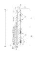
図1に、光電変換装置100の平面レイアウト図を示す。光電変換装置100は、受光領域10と、被遮光領域20と、周辺回路領域30を含む。被遮光領域20は、受光領域10の外側に設けられた領域である。受光領域10および被遮光領域20には、複数の画素が2次元アレイ状に配列されている。画素は、少なくとも1つの光電変換部と、光電変換部にて生じた信号を読み出すための読み出し回路を含む。読み出し回路は、例えば、光電変換部と電気的に接続した転送トランジスタや、光電変換部と電気的に接続したゲート電極を有する増幅トランジスタや、光電変換部をリセットするためのリセットトランジスタを含む。周辺回路領域30は、受光領域10の動作の制御や受光領域10から読み出された信号の処理を行う周辺回路が設けられた領域であり、例えば、増幅回路、水平走査回路、および垂直走査回路を含む。被遮光領域20と周辺回路領域30は、半導体基板の表面に対して垂直な方向から見た場合に、遮光膜によって覆われている。一方、受光領域10は、半導体基板の表面に対して垂直な方向から見た場合(平面視した場合)に、遮光膜が設けられていないか、画素毎に開口されている遮光膜が設けられており、光が半導体領域に到達する。被遮光領域20に配された画素の少なくとも一部はオプティカルブラック画素(OPB画素)であり、OPB画素にて得られた信号はノイズ信号として利用される。つまり、各領域は2つに分けることが出来る。1つの領域101は、受光領域10を含み、もう1つの領域102は非遮光領域20と周辺回路領域30を含む。領域102は領域101の外側に設けられている。
FIG. 1 is a plan layout diagram of the
図2は、図1に示した平面レイアウト図におけるA−A’部分の断面を示す図である。A−A’部分は、受光領域10を含む領域101と、周辺回路領域30を含む領域102に渡る部分である。領域101には、複数の光電変換部218が半導体基板(以下、単に基板ともいう)201の上に設けられている。ここでは、2つの光電変換部を図示している。2つの光電変換部218は、基板201の表面202に沿って配列している。ここで、表面202に対して垂直な方向であって、表面202から離れる方向を上方向とし、表面202に対して垂直な方向であって、基板内部に向かう方向を下方向とする。また、表面202を基準とした場合、上方向の距離は高さとも言える。
FIG. 2 is a diagram showing a cross-section of the A-A ′ portion in the plan layout diagram shown in FIG. 1. The A-A ′ portion is a portion extending over the
光電変換部218は、電極219と、光電変換層220と、電極221を含んで構成されている。電極219は下部電極とも称し、アルミニウムや銅を主成分とする導電体からなる。電極221は上部電極とも称し、透明導電材料からなることが望ましく、例えば、ITO(Indium Tin Oxide)やポリイミドを主成分とする導電体からなる。そして、電極221は、電極226を介して、周辺回路と電気的に接続される。光電変換層220は、例えば、無機材料あるいは有機材料からなる光電変換可能な材料からなる。光電変換層220として、例えば、無機材料の場合には、アモルファスシリコン層、アモルファスセレン層、量子ドット層、化合物半導体層等を適宜選択できる。光電変換層220の材料として、例えば、有機材料の場合には、金属錯体色素、シアニン系色素等の色素等がある。また、別の有機材料としては、アクリジン、クマリン、トリフェニルメタン、フラーレン、アルミニウムキノリン、ポリパラフェニレンビニレン、ポリフルオレン、ポリビニルカルバゾール、ポリチオール、ポリピロール、ポリチオフェンなどの誘導体がある。本実施形態では、量子ドット層である。例えば、量子ドット層は、AlGaAsあるいはGaAsのバッファ材と、InAsあるいはInGaAsの量子ドットからなる。領域101の基板201には、複数のトランジスタ216が配されている。領域102の基板201には、複数のトランジスタ217が配されている。複数のトランジスタ217は、上述の処理回路を構成する。
The
基板201の表面202の上には、配線構造体203が設けられている。配線構造体203は、少なくとも1層の配線層を有する。ここでは、配線構造体203は、領域101と領域102に連続して設けられた絶縁膜204〜206と、領域102に設けられ、領域101には設けられていない絶縁膜207、208を有する。更に、配線構造体203は、領域101と領域102の両方に設けられた配線層209、210と、領域102に設けられ、領域101には設けられていない配線層211、212、213を有する。各配線層は、互いに異なる高さに位置し、少なくとも1つの配線パターンを有する。配線層212は、例えば、領域102において、領域102の少なくとも一部において領域102の基板へ入射し得る光を低減する遮光膜として機能する。また、配線層213は、外部との接続のための端子(パッド部)となる。保護膜214は、領域101の光電変換部218の上から配線層213を覆い、配線層213の上面の一部を露出させる開口215を有する。領域101の保護膜214の上には、カラーフィルタ層222とマイクロレンズ層223が設けられている。カラーフィルタ層222は、複数のカラーフィルタを含み、マイクロレンズ層223は複数のマイクロレンズを含む。
A
光電変換部218の電極219は、配線層210と、導電体からなるプラグとを介し、基板201に設けられた読み出し回路のトランジスタの一部に電気的に接続されている。ここで、電極219は、下面219aと上面219bを有する。下面219aはプラグ224(接続部)と接し、電気的に接続されている。プラグ224は、他の配線層を介して、基板201に設けられたトランジスタの一部に電気的に接続される。光電変換部218にて生じた信号は、配線層210を介して、トランジスタの一部に伝達される。電極221は、電極224を介して配線層210と電気的に接続される。この時、領域102の上には、電極219の下面219aよりも高い位置に配線層212、213が配されている。配線層212が有する配線パターンは、下面212aと上面212bを有する。配線層212の配線パターンは、配線層と、導電体からなるプラグとを介し、基板201に設けられた周辺回路と電気的に接続されている。配線層212の配線パターンの下面212aは、プラグ225(接続部)と接し、電気的に接続されている。プラグ225は、他の配線層を介して、基板201に設けられた周辺回路のトランジスタの一部に電気的に接続される。
The
ここで、電極219の下面219aは、表面202から距離d1離れた位置に配され、配線層212の下面212aは、表面202から距離d2離れた位置に配されている。そして、距離d1は距離d2よりも短い(d1<d2)。ここで、距離は、基板201の表面202から各面までの最短距離である。これは、電極219と基板201に設けられた読み出し回路との間の信号経路が、配線層212と基板201に設けられた周辺回路との間の信号経路よりも短いとも言える。この電極219と基板201との距離が長いと配線層とプラグによって形成される信号経路の長さが増えるので、導電体の面積が増加して容量が増えてしまうため、距離d1は距離d2よりも短いことが望ましい。このような構成によって、光電変換部の信号経路の容量の増大を低減することが可能となる。よって、例えば、光電変換部218がトランジスタ216のソースに電気的に接続する場合には、時定数(RC)が小さくなるため、トランジスタ216を介して信号経路をリセットする際の速度が向上する。また、光電変換層と同一ノードの容量が低減されるため、熱雑音(KTCノイズ)を低減することが可能となる。更に、電極219と基板201との間に存在し得る配線層の数(配線層の数がゼロ、すなわち配線層が設けられていない場合を含む)が、配線層212と基板201との間に存在する配線層の数よりも少ない。よって、電極219から基板202までの信号経路が通る配線層の数が少ないため、信号経路と各配線層との間に生じる寄生容量を低減することが可能である。なお、領域102の周辺回路には多くの回路が設けられているため、配線層の層数を維持または多くすることが望まれる。本実施形態の構成によれば、領域102の配線層の数を減らすことなく、信号経路の容量の増大を低減することが可能となる。なお、このような構成によって、光電変換部218と基板201との間の信号経路における抵抗(R)も低減することが可能である。
Here, the
本実施形態では、電極221の上面と表面202との距離は、配線層212の下面212aと表面202との距離よりも短い。このような構成によって、光電変換部218と基板201との距離を短くすることが出来る。また、電極221の上面と表面202との距離は、配線層212の下面212aと表面202との距離よりも長く、配線層212の上面212bと表面202との距離d3よりも短くてもよい。このような構成であれば、領域101と領域102との段差を低減することが出来る。また、更に、電極221の上面と表面202との距離は、配線層212の上面212bと表面202との距離と等しくてもよい。このような構成によって、更に、領域101と領域102との段差を低減することが出来る。また、電極221は、電極219と同一の高さに位置していてもよい。また、領域101と領域102を有する構成を示したが、例えば、領域101内において、電極219の下面219aと基板201との距離が、配線層210の下面と基板201との距離よりも小さくてもよい。
In the present embodiment, the distance between the upper surface of the
また、本実施形態では、読み出し回路のトランジスタとして転送トランジスタの例を説明し、光電変換部218の電極219は転送トランジスタのソースに接続される構成を示した。転送トランジスタのドレインは、信号線や増幅回路に接続されうる。光電変換部218の電極219が接続される部分は、例えば、ソースフォロワ回路を構成する増幅トランジスタのゲート電極と接続してもよく、これらの構成に限らない。
In this embodiment, an example of a transfer transistor is described as the transistor of the readout circuit, and the
(第2の実施形態)
第2の実施形態について図3を用いて説明する。本実施形態において、第1の実施形態と同様の構成については、同一の符号を付し、説明を省略する。
(Second Embodiment)
A second embodiment will be described with reference to FIG. In the present embodiment, the same components as those in the first embodiment are denoted by the same reference numerals, and description thereof is omitted.
本実施形態の光電変換部318は、電極319と、その上に設けられた光電変換層320と、光電変換層320の上に設けられた電極321を有する。ここで、電極319は、基板201の表面202に直接接して設けられており、半導体領域301と電気的に接続されている。つまり、本実施形態においては、電極319の下面と接する接続部は設けられていない。絶縁膜304は、表面202の上に設けられ、領域101と領域102に渡って設けられている。光電変換層320は、絶縁膜304に設けられた開口を埋め、電極319と電気的に接続され、領域101において絶縁膜304の開口以外の上を覆っている。電極321は、光電変換層320を覆い、領域102に設けられた配線層309と電気的に接続される。保護膜214は、領域101から領域102に渡って、電極321の上から配線層309の上に延在する。保護膜214は開口215を有し、配線層309の上面の一部を露出させており、配線層309は端子として機能する。ここで、配線層309に含まれる別の配線パターンの下面と接する接続部(不図示)を有していてもよい。本実施形態においては、電極319の下面319aは配線層309の下面309aよりも基板201の近くに位置する。つまり、下面319aと表面202との距離が、下面309aと表面202との距離よりも短い。また、電極319の上面319bは配線層309の下面309aよりも基板201の近くに位置し、電極319の上面319bは配線層309の上面309bよりも基板201の近くに位置する。つまり、上面319bと表面202との距離が、下面309aと表面202との距離よりも短く、上面319bと表面202との距離が、上面309bと表面202との距離よりも短い。このような構成によって、より信号経路の容量の増大を抑制することが可能となる。
The photoelectric conversion unit 318 of this embodiment includes an electrode 319, a photoelectric conversion layer 320 provided thereon, and an electrode 321 provided on the photoelectric conversion layer 320. Here, the electrode 319 is provided in direct contact with the
(第3の実施形態)
第3の実施形態について図4を用いて説明する。本実施形態において、第1の実施形態と同様の構成については、同一の符号を付し、説明を省略する。
(Third embodiment)
A third embodiment will be described with reference to FIG. In the present embodiment, the same components as those in the first embodiment are denoted by the same reference numerals, and description thereof is omitted.
本実施形態の光電変換部418は、電極219と光電変換層220との間に、絶縁膜401を有するMIS型の構造を有する点で、第1の実施形態と異なる。絶縁膜401は、シリコン酸化膜からなる、コンフォーマルな膜であり、電極219の形状を踏襲する上面を有する。このような構成においても、第1の実施形態と同様に信号経路の容量の増大を抑制することが可能である。
The
(第4の実施形態)
第4の実施形態について図5を用いて説明する。本実施形態において、第1の実施形態と同様の構成については、同一の符号を付し、説明を省略する。
(Fourth embodiment)
A fourth embodiment will be described with reference to FIG. In the present embodiment, the same components as those in the first embodiment are denoted by the same reference numerals, and description thereof is omitted.
本実施形態の光電変換部518は、電極519と、電極519の上に設けられた光電変換層520と、光電変換層520の上に設けられた電極521を有する。ここで、領域101の絶縁膜505と絶縁膜506が開口を有し、光電変換部518は開口の側面と底面に沿って設けられている。そして、開口の中の光電変換部518の上に保護膜514が設けられている。
The
電極519の下面519aと表面202との距離d4は、配線層212の下面212aと表面202との距離d2よりも短い。このような構成においても、信号経路の容量の増大を抑制することが可能となる。
A distance d4 between the
なお、保護膜514は、開口の平坦化層としても機能しうる。電極519の上面519aは配線層212の下面212aよりも表面202に近い。すなわち、上面519aと表面202との距離は、下面212aと表面202との距離よりも短い。
Note that the
(第5の実施形態)
第5の実施形態について、図6を用いて説明する。本実施形態において、第1の実施形態と同様の構成については、同一の符号を付し、説明を省略する。
(Fifth embodiment)
A fifth embodiment will be described with reference to FIG. In the present embodiment, the same components as those in the first embodiment are denoted by the same reference numerals, and description thereof is omitted.
本実施形態の光電変換部618は、電極219と、電極219の上に設けられた光電変換層620と、光電変換層620の上に設けられた電極221と、電極219の上面の一部を露出する開口を有する絶縁膜601とを有する。絶縁膜601の開口の側面は電極219の上に位置し、光電変換層620と界面を構成し、導波路として機能し得る。この時、絶縁膜601は、シリコン酸化膜からなり、光電変換層620は、量子ドット膜からなる。これらの材料は、絶縁膜601の屈折率は、光電変換層620の屈折率よりも低ければ良い。このような構成によって、光が隣接する光電変換層へ混入することを低減することが出来る。
The
また、本実施形態では、光電変換層620は、絶縁膜601の上面の上にも延在し、その上面と下面との距離d6は、開口の中の光電変換層620の上面と下面との距離d5よりも短い。しかし、光電変換層620の上面が絶縁膜601の上面と面一であってもよい。
In the present embodiment, the
(第6の実施形態)
第6の実施形態について、図7を用いて説明する。第6の実施形態は、第5の実施形態にて説明した導波路構造を有する構成を示している。本実施形態において、第1の実施形態及び第5の実施形態と同様の構成については、同一の符号を付し、説明を省略する。
(Sixth embodiment)
A sixth embodiment will be described with reference to FIG. The sixth embodiment shows a configuration having the waveguide structure described in the fifth embodiment. In the present embodiment, the same components as those in the first embodiment and the fifth embodiment are denoted by the same reference numerals, and description thereof is omitted.
本実施形態の光電変換部718は、電極219と、電極219の上に設けられた光電変換層720と、光電変換層720の上に設けられた電極221と、電極219の上面の一部を露出する開口を有する絶縁膜701を有する。この絶縁膜701と光電変換層720は、第5の実施形態と同様に導波路として機能し得る。ここで、カラーフィルタ層222は、第1の色に対応する第1カラーフィルタ722aと、第1の色と異なる第2の色に対応する第2カラーフィルタ722bとを含む。ここで、第1カラーフィルタ722aと、第2カラーフィルタ722bは、互いに異なる分光透過率プロファイルを有する。
The
このような構成において、第1のカラーフィルタ722aに対応する光電変換部718は、絶縁膜701の上面における開口の幅d7を有し、第2のカラーフィルタ722bに対応する光電変換部718は、絶縁膜701の上面における開口の幅d8を有する。ここで、開口の幅d7と開口の幅d8は互いに異なる。これら幅の関係について説明する。例えば、可視光に対応したカラーフィルタ層722において、白色光を入射したときに感度をそろえたい場合には次のようにする。第1のカラーフィルタ722aを透過する光が、第2のカラーフィルタ722bを透過する光よりも少ない場合には、幅d7を幅d8よりも広くする。また、例えば、可視光に対応したカラーフィルタ層722において、光の回折による混色を低減したい場合には次のようにする。第2のカラーフィルタ722bを透過する光の波長が第1のカラーフィルタ722aを透過する光の波長よりも長い場合には、幅d7を幅d8よりも広くする。
In such a configuration, the
このように、カラーフィルタ層722の特性に応じて、開口の幅を変えることが可能である。なお、開口の幅とは、表面202に平行な方向における長さであり、導波路の幅でもある。本実施形態では絶縁膜701の上面における幅を変更したが、それ以外の部分で幅の大きさを変更してもよい。
As described above, the opening width can be changed in accordance with the characteristics of the color filter layer 722. The opening width is a length in a direction parallel to the
(第7の実施形態)
第7の実施形態について、図8を用いて説明する。第7の実施形態は、第5の実施形態にて説明した導波路構造を有する構成であり、導波路の高さを変えた点が異なる。第7の実施形態は、第6の実施形態とは、導波路の幅を変えるか、高さを変えるかで異なる。本実施形態において、第1の実施形態、第5の実施形態、及び第6の実施形態と同様の構成については、同一の符号を付し、説明を省略する。
(Seventh embodiment)
A seventh embodiment will be described with reference to FIG. The seventh embodiment is a configuration having the waveguide structure described in the fifth embodiment, and is different in that the height of the waveguide is changed. The seventh embodiment differs from the sixth embodiment in that the width of the waveguide is changed or the height is changed. In the present embodiment, the same components as those in the first embodiment, the fifth embodiment, and the sixth embodiment are denoted by the same reference numerals, and description thereof is omitted.
本実施形態の光電変換部818は、電極219と、電極819の上に設けられた光電変換層820と、光電変換層720の上に設けられた電極221と、電極219の上面の一部を露出する開口を有する絶縁膜801とを有する。この絶縁膜801と光電変換層820は、第5の実施形態と同様に導波路として機能し得る。ここで、カラーフィルタ層222は、第1の色に対応する第1カラーフィルタ822aと、第1の色と異なる第2の色に対応する第2カラーフィルタ822bとを含む。ここで、第1カラーフィルタ822aと、第2カラーフィルタ822bは、互いに異なる分光透過率プロファイルを有する。
The photoelectric conversion unit 818 of this embodiment includes an
このような構成において、第1のカラーフィルタ822aに対応する光電変換部818の電極の下には、絶縁膜802が設けられている。電極819の下面819aは、プラグ224a(接続部)と接する。この絶縁膜802によって、電極819の下面819aと表面202との距離は、距離d9となる。第1のカラーフィルタ822aに対応する光電変換層820は、電極819の上面819bから絶縁膜801の上面の高さまでの距離d11だけの厚みを有する。一方、第2のカラーフィルタ822bに対応する光電変換部818は、絶縁膜802の上には設けられておらず、電極819の下面819bと表面202との距離は、距離d10を有する。ここで、距離d9は距離d10よりも大きい。第2のカラーフィルタ822bに対応する光電変換層820は、電極819の上面819bから絶縁膜801の上面の高さまでの距離d12だけの厚みを有する。ここで距離d11は距離d12よりも薄い。このようにカラーフィルタ層722の特性に応じて、導波路の高さを変えることが可能である。
In such a structure, an insulating
導波路の高さの関係について説明する。例えば、カラーフィルタ層822が含む各カラーフィルタと、光電変換層における光の吸収とに応じて、深さを変えることが望ましい。例えば、第2のカラーフィルタ822bが、第1のカラーフィルタ822aよりも波長の長い光を透過するために設けられ、光電変換層820がアモルファスシリコン層の場合には、距離d12は距離d11よりも大きくすることが望ましい。
The relationship of the height of the waveguide will be described. For example, it is desirable to change the depth in accordance with each color filter included in the color filter layer 822 and light absorption in the photoelectric conversion layer. For example, when the
このように、カラーフィルタ層822の特性に応じて、導波路の高さを変えることが可能である。なお、光電変換層820は、絶縁膜801の上面の上にも延在しているが、開口の中のみ、すなわち絶縁膜801の上面と面一の上面を有する構成でもよい。
Thus, the height of the waveguide can be changed in accordance with the characteristics of the color filter layer 822. Note that the photoelectric conversion layer 820 also extends over the top surface of the insulating
なお、本実施形態の製造方法は、絶縁膜206を形成した後に、絶縁膜802を形成し、電極819を形成することで製造可能である。また、本実施形態と第6の実施形態とを組み合わせてもよい。
In addition, the manufacturing method of this embodiment can be manufactured by forming the insulating
(第8の実施形態)
第8の実施形態について、図9(a)、図9(b)を用いて説明する。第8の実施形態は、第6の実施形態や第7の実施形態とは、光電変換層の厚みが異なる。本実施形態において、第1の実施形態、第6の実施形態、及び第7の実施形態と同様の構成については、同一の符号を付し、説明を省略する。
(Eighth embodiment)
The eighth embodiment will be described with reference to FIGS. 9A and 9B. The eighth embodiment differs from the sixth embodiment and the seventh embodiment in the thickness of the photoelectric conversion layer. In the present embodiment, the same components as those in the first embodiment, the sixth embodiment, and the seventh embodiment are denoted by the same reference numerals, and description thereof is omitted.
図9(a)は、第6の実施形態に対応する図である。図9(a)において、光電変換部918は、電極219と、絶縁膜701と、光電変換層920と、電極921とを含む。ここで、光電変換層920は、絶縁膜701の上面から、絶縁膜の開口の側面を覆い、電極219の上を覆っており、絶縁膜701の形状を踏襲した上面を有するコンフォーマルな膜である。更に、電極921も同様に、光電変換層920の上面の形状を踏襲した上面を有するコンフォーマルな膜として形成されている。そして、保護膜914が、電極921の上面に沿って、電極921の上面の窪みを埋め、領域101において平坦化膜として機能している。
FIG. 9A is a diagram corresponding to the sixth embodiment. 9A, the
図9(b)は、第7の実施形態に対応する。図9(b)において、光電変換部1018は、電極819と、絶縁膜801と、光電変換層1020と、電極1021とを含む。ここで、光電変換層1020は、絶縁膜801の上面から、絶縁膜の開口の側面を覆い、電極819の上を覆っており、絶縁膜801の形状を踏襲した上面を有するコンフォーマルな膜である。更に、電極1021も同様に、光電変換層1020の上面の形状を踏襲した上面を有するコンフォーマルな膜として形成されている。そして、保護膜1014が、電極1021の上面に沿って、電極1021の上面の窪みを埋め、領域101において平坦化膜として機能している。このような構成においても、第1の実施形態と同様に信号経路の容量の増大を抑制することが可能となる。
FIG. 9B corresponds to the seventh embodiment. In FIG. 9B, the
以下、上記の各実施形態に係る光電変換装置の応用例として、該光電変換装置が組み込まれた撮像システムについて例示的に説明する。撮像システムの概念には、撮影を主目的とするカメラなどの装置のみならず、撮影機能を補助的に備える装置(例えば、パーソナルコンピュータ、携帯端末)も含まれる。撮像システムは、上記の実施形態として例示された本発明に係る光電変換装置と、該光電変換装置から出力される信号を処理する信号処理部とを含む。該信号処理部は、例えば、A/D変換器、および、該A/D変換器から出力されるデジタルデータを処理するプロセッサを含みうる。 Hereinafter, as an application example of the photoelectric conversion device according to each of the embodiments described above, an imaging system in which the photoelectric conversion device is incorporated will be exemplarily described. The concept of the imaging system includes not only a device such as a camera whose main purpose is photographing, but also a device (for example, a personal computer or a portable terminal) that is supplementarily provided with a photographing function. The imaging system includes the photoelectric conversion device according to the present invention exemplified as the above embodiment, and a signal processing unit that processes a signal output from the photoelectric conversion device. The signal processing unit may include, for example, an A / D converter and a processor that processes digital data output from the A / D converter.
各実施形態において、基板として半導体基板を例に説明を行ったが、回路が形成されたガラス基板やフレキシブル基板等であってもよい。また、下部電極よりも高い位置にある配線層が存在する領域についても領域102に限定されない。しかし、領域102に配線層が存在する場合には、各実施形態の構成の製造が容易となる。また、絶縁膜や保護膜は単層でも多層でもよく、各層が異なる材料からなっていてもよい。その他、第1〜第8の実施形態は、適宜変更、組み合わせが可能である。
In each embodiment, the semiconductor substrate has been described as an example of the substrate. However, a glass substrate or a flexible substrate on which a circuit is formed may be used. Further, the region where the wiring layer located higher than the lower electrode is not limited to the
101 領域
102 領域
201 基板
202 表面
218 光電変換部
219 電極
219a 下面
219b 上面
220 光電変換層
221 電極
214 保護膜
203 配線構造体
204〜208 絶縁膜
212a 下面
212b 上面
209〜213 配線層
DESCRIPTION OF
Claims (13)
前記表面の上に設けられ、それぞれが絶縁膜と配線パターンとを含む複数の配線層と、
前記配線層の上に設けられ、それぞれが第1の電極と前記第1の電極の上に設けられた光電変換層とを含む、第1の光電変換部及び第2の光電変換部と、
前記第1の光電変換部の上に設けられた第1のカラーフィルタと、
前記第2の光電変換部の上に設けられ、前記第1のカラーフィルタとは異なる色の光を透過する第2のカラーフィルタと、
前記基板に設けられ、前記第1の光電変換部に含まれる光電変換層で生じた信号を読み出す第1の読み出し回路と、
前記基板に設けられ、前記第2の光電変換部に含まれる光電変換層で生じた信号を読み出す第2の読み出し回路と、
前記第1の光電変換部及び前記第2の光電変換部と重ならない領域であって、前記基板に設けられた周辺回路を有する周辺回路領域と、
前記周辺回路領域に設けられた電極と、を備え、
前記第1の光電変換部が有する前記第1の電極の下面と、前記第2の光電変換部が有する前記第1の電極の下面は、前記複数の配線層のうちの同一の配線層の前記配線パターンの上面に接しており、
前記第1の電極の下面と前記表面との間に設けられた配線層の数は、前記周辺回路領域に設けられた電極の下面と前記表面との間に設けられた配線層の数よりも少ないことを特徴とする光電変換装置。 A substrate having a surface;
A plurality of wiring layers provided on the surface, each including an insulating film and a wiring pattern;
A first photoelectric conversion unit and a second photoelectric conversion unit provided on the wiring layer, each including a first electrode and a photoelectric conversion layer provided on the first electrode;
A first color filter provided on the first photoelectric conversion unit;
A second color filter that is provided on the second photoelectric conversion unit and transmits light of a color different from that of the first color filter;
A first readout circuit that is provided on the substrate and reads out a signal generated in a photoelectric conversion layer included in the first photoelectric conversion unit;
A second readout circuit that is provided on the substrate and reads out a signal generated in a photoelectric conversion layer included in the second photoelectric conversion unit;
A peripheral circuit region having a peripheral circuit provided on the substrate, the region not overlapping the first photoelectric conversion unit and the second photoelectric conversion unit;
An electrode provided in the peripheral circuit region,
The lower surface of the first electrode included in the first photoelectric conversion unit and the lower surface of the first electrode included in the second photoelectric conversion unit are formed on the same wiring layer of the plurality of wiring layers. It is in contact with the upper surface of the wiring pattern,
The number of wiring layers provided between the lower surface of the first electrode and the surface is larger than the number of wiring layers provided between the lower surface of the electrode provided in the peripheral circuit region and the surface. A photoelectric conversion device characterized by a small amount.
前記プラグの上面は前記パッド電極の下面と接し、
前記プラグの下面は前記電極の上面と接することを特徴とする請求項11に記載の光電変換装置。 Having a plug made of a conductor;
The upper surface of the plug is in contact with the lower surface of the pad electrode,
The photoelectric conversion device according to claim 1 1 lower surface of said plug, characterized in that contact with the upper surface of the electrode.
前記光電変換装置からの信号を処理する信号処理部と、を有する撮像システム。 The photoelectric conversion device according to any one of claims 1 to 12,
A signal processing unit that processes a signal from the photoelectric conversion device;
Priority Applications (2)
| Application Number | Priority Date | Filing Date | Title |
|---|---|---|---|
| JP2014156785A JP6562600B2 (en) | 2014-07-31 | 2014-07-31 | Photoelectric conversion device and imaging system |
| US14/811,610 US9812476B2 (en) | 2014-07-31 | 2015-07-28 | Photoelectric transducer and imaging system |
Applications Claiming Priority (1)
| Application Number | Priority Date | Filing Date | Title |
|---|---|---|---|
| JP2014156785A JP6562600B2 (en) | 2014-07-31 | 2014-07-31 | Photoelectric conversion device and imaging system |
Publications (3)
| Publication Number | Publication Date |
|---|---|
| JP2016033977A JP2016033977A (en) | 2016-03-10 |
| JP2016033977A5 JP2016033977A5 (en) | 2017-08-31 |
| JP6562600B2 true JP6562600B2 (en) | 2019-08-21 |
Family
ID=55180849
Family Applications (1)
| Application Number | Title | Priority Date | Filing Date |
|---|---|---|---|
| JP2014156785A Active JP6562600B2 (en) | 2014-07-31 | 2014-07-31 | Photoelectric conversion device and imaging system |
Country Status (2)
| Country | Link |
|---|---|
| US (1) | US9812476B2 (en) |
| JP (1) | JP6562600B2 (en) |
Families Citing this family (6)
| Publication number | Priority date | Publication date | Assignee | Title |
|---|---|---|---|---|
| WO2017122538A1 (en) * | 2016-01-13 | 2017-07-20 | ソニー株式会社 | Photoelectric conversion element, imaging element, and electronic device |
| WO2017169231A1 (en) * | 2016-03-31 | 2017-10-05 | ソニー株式会社 | Image capturing element and electronic device |
| US10319765B2 (en) * | 2016-07-01 | 2019-06-11 | Canon Kabushiki Kaisha | Imaging device having an effective pixel region, an optical black region and a dummy region each with pixels including a photoelectric converter |
| JP7084700B2 (en) * | 2017-06-16 | 2022-06-15 | キヤノン株式会社 | Photoconverter and scanner |
| CN110098218A (en) * | 2018-01-31 | 2019-08-06 | 松下知识产权经营株式会社 | Photographic device |
| JP2021019058A (en) | 2019-07-18 | 2021-02-15 | キヤノン株式会社 | Photoelectric conversion device and apparatus |
Family Cites Families (18)
| Publication number | Priority date | Publication date | Assignee | Title |
|---|---|---|---|---|
| JPS5672584A (en) * | 1979-11-16 | 1981-06-16 | Matsushita Electric Ind Co Ltd | Solid-state image pickup device |
| JP4578792B2 (en) * | 2003-09-26 | 2010-11-10 | 富士通セミコンダクター株式会社 | Solid-state imaging device |
| JP4500574B2 (en) * | 2004-03-30 | 2010-07-14 | 富士フイルム株式会社 | Wide dynamic range color solid-state imaging device and digital camera equipped with the solid-state imaging device |
| US7268369B2 (en) | 2004-07-06 | 2007-09-11 | Fujifilm Corporation | Functional device and method for producing the same |
| JP2006245284A (en) * | 2005-03-03 | 2006-09-14 | Fuji Photo Film Co Ltd | Photoelectric conversion film stacked type solid-state image sensing device and method of manufacturing same |
| JP4911445B2 (en) | 2005-06-29 | 2012-04-04 | 富士フイルム株式会社 | Organic and inorganic hybrid photoelectric conversion elements |
| JP2007208840A (en) | 2006-02-03 | 2007-08-16 | Fujifilm Corp | Solid-state imaging device |
| JP2007273586A (en) * | 2006-03-30 | 2007-10-18 | Toshiba Corp | Solid-state imaging device |
| JP2008004684A (en) * | 2006-06-21 | 2008-01-10 | Toshiba Corp | Solid-state imaging device |
| JP2008053366A (en) * | 2006-08-23 | 2008-03-06 | Toshiba Corp | Solid state imaging apparatus |
| JP4315457B2 (en) * | 2006-08-31 | 2009-08-19 | キヤノン株式会社 | Photoelectric conversion device and imaging system |
| JP4285551B2 (en) * | 2007-02-19 | 2009-06-24 | セイコーエプソン株式会社 | ELECTRO-OPTICAL DEVICE, MANUFACTURING METHOD THEREOF, AND ELECTRONIC DEVICE |
| JP5388478B2 (en) * | 2008-05-20 | 2014-01-15 | 株式会社東芝 | Semiconductor device |
| JP5302644B2 (en) * | 2008-12-03 | 2013-10-02 | キヤノン株式会社 | Imaging apparatus and imaging system |
| JP5365221B2 (en) * | 2009-01-29 | 2013-12-11 | ソニー株式会社 | Solid-state imaging device, manufacturing method thereof, and imaging device |
| JP5533046B2 (en) * | 2010-03-05 | 2014-06-25 | ソニー株式会社 | Solid-state imaging device, method for manufacturing solid-state imaging device, driving method for solid-state imaging device, and electronic apparatus |
| WO2012004923A1 (en) * | 2010-07-09 | 2012-01-12 | パナソニック株式会社 | Solid-state image pickup device and method for driving solid-state image pickup device |
| JP2012209421A (en) * | 2011-03-30 | 2012-10-25 | Sony Corp | Solid-state image pickup device and electronic equipment |
-
2014
- 2014-07-31 JP JP2014156785A patent/JP6562600B2/en active Active
-
2015
- 2015-07-28 US US14/811,610 patent/US9812476B2/en active Active
Also Published As
| Publication number | Publication date |
|---|---|
| US9812476B2 (en) | 2017-11-07 |
| US20160035767A1 (en) | 2016-02-04 |
| JP2016033977A (en) | 2016-03-10 |
Similar Documents
| Publication | Publication Date | Title |
|---|---|---|
| US10511751B2 (en) | Photoelectric conversion apparatus and image pickup system | |
| JP6562600B2 (en) | Photoelectric conversion device and imaging system | |
| US11031424B2 (en) | Image sensor with selective light-shielding for reference pixels | |
| US10186533B2 (en) | Solid-state imaging device, camera module and electronic apparatus | |
| US9906743B2 (en) | Solid-state imaging apparatus and imaging system having a light shielding portion | |
| US9105544B2 (en) | Solid-state imaging device | |
| JP6188281B2 (en) | Photoelectric conversion device | |
| KR102136852B1 (en) | CMOS Image Sensor based on a Thin-Film on ASIC and operating method thereof | |
| US9130180B2 (en) | Image sensor with organic photoelectric layer | |
| US20090321800A1 (en) | Semiconductor device including solid state image pickup device, and portable electronic apparatus | |
| JP6576025B2 (en) | Photoelectric conversion device and imaging system | |
| JP2014146820A (en) | Solid-state image pickup device | |
| JP2019009154A (en) | Photoelectric conversion device and equipment | |
| US20110115043A1 (en) | Solid-state image sensor and imaging device | |
| US20140110771A1 (en) | Solid-state imaging device and semiconductor device | |
| JP6813971B2 (en) | Photoelectric conversion device and imaging system | |
| KR102296736B1 (en) | Staked image sensor | |
| JP2019165250A (en) | Photoelectric conversion device | |
| JP2013197333A (en) | Solid-state imaging device, camera, and electronic apparatus | |
| JP2009064982A (en) | Solid-state imaging element | |
| JP2022167804A (en) | image sensor | |
| JP2014239183A (en) | Photoelectric conversion device | |
| JP2022146934A (en) | image sensor | |
| JP2019075441A (en) | Photoelectric conversion device and equipment |
Legal Events
| Date | Code | Title | Description |
|---|---|---|---|
| A521 | Request for written amendment filed |
Free format text: JAPANESE INTERMEDIATE CODE: A523 Effective date: 20170721 |
|
| A621 | Written request for application examination |
Free format text: JAPANESE INTERMEDIATE CODE: A621 Effective date: 20170721 |
|
| A977 | Report on retrieval |
Free format text: JAPANESE INTERMEDIATE CODE: A971007 Effective date: 20180322 |
|
| A131 | Notification of reasons for refusal |
Free format text: JAPANESE INTERMEDIATE CODE: A131 Effective date: 20180417 |
|
| A521 | Request for written amendment filed |
Free format text: JAPANESE INTERMEDIATE CODE: A523 Effective date: 20180614 |
|
| A131 | Notification of reasons for refusal |
Free format text: JAPANESE INTERMEDIATE CODE: A131 Effective date: 20181127 |
|
| A521 | Request for written amendment filed |
Free format text: JAPANESE INTERMEDIATE CODE: A523 Effective date: 20190119 |
|
| TRDD | Decision of grant or rejection written | ||
| A01 | Written decision to grant a patent or to grant a registration (utility model) |
Free format text: JAPANESE INTERMEDIATE CODE: A01 Effective date: 20190625 |
|
| A61 | First payment of annual fees (during grant procedure) |
Free format text: JAPANESE INTERMEDIATE CODE: A61 Effective date: 20190723 |
|
| R151 | Written notification of patent or utility model registration |
Ref document number: 6562600 Country of ref document: JP Free format text: JAPANESE INTERMEDIATE CODE: R151 |