JP6553472B2 - Contactor - Google Patents
Contactor Download PDFInfo
- Publication number
- JP6553472B2 JP6553472B2 JP2015194768A JP2015194768A JP6553472B2 JP 6553472 B2 JP6553472 B2 JP 6553472B2 JP 2015194768 A JP2015194768 A JP 2015194768A JP 2015194768 A JP2015194768 A JP 2015194768A JP 6553472 B2 JP6553472 B2 JP 6553472B2
- Authority
- JP
- Japan
- Prior art keywords
- flexible substrate
- contact
- springs
- contact portions
- contactor
- Prior art date
- Legal status (The legal status is an assumption and is not a legal conclusion. Google has not performed a legal analysis and makes no representation as to the accuracy of the status listed.)
- Active
Links
Images


Classifications
-
- G—PHYSICS
- G01—MEASURING; TESTING
- G01R—MEASURING ELECTRIC VARIABLES; MEASURING MAGNETIC VARIABLES
- G01R1/00—Details of instruments or arrangements of the types included in groups G01R5/00 - G01R13/00 and G01R31/00
- G01R1/02—General constructional details
- G01R1/06—Measuring leads; Measuring probes
- G01R1/067—Measuring probes
- G01R1/06711—Probe needles; Cantilever beams; "Bump" contacts; Replaceable probe pins
- G01R1/06716—Elastic
- G01R1/06722—Spring-loaded
-
- G—PHYSICS
- G01—MEASURING; TESTING
- G01R—MEASURING ELECTRIC VARIABLES; MEASURING MAGNETIC VARIABLES
- G01R1/00—Details of instruments or arrangements of the types included in groups G01R5/00 - G01R13/00 and G01R31/00
- G01R1/02—General constructional details
- G01R1/04—Housings; Supporting members; Arrangements of terminals
- G01R1/0408—Test fixtures or contact fields; Connectors or connecting adaptors; Test clips; Test sockets
- G01R1/0433—Sockets for IC's or transistors
- G01R1/0441—Details
- G01R1/0466—Details concerning contact pieces or mechanical details, e.g. hinges or cams; Shielding
-
- G—PHYSICS
- G01—MEASURING; TESTING
- G01R—MEASURING ELECTRIC VARIABLES; MEASURING MAGNETIC VARIABLES
- G01R1/00—Details of instruments or arrangements of the types included in groups G01R5/00 - G01R13/00 and G01R31/00
- G01R1/02—General constructional details
- G01R1/06—Measuring leads; Measuring probes
- G01R1/067—Measuring probes
- G01R1/073—Multiple probes
- G01R1/07307—Multiple probes with individual probe elements, e.g. needles, cantilever beams or bump contacts, fixed in relation to each other, e.g. bed of nails fixture or probe card
- G01R1/07314—Multiple probes with individual probe elements, e.g. needles, cantilever beams or bump contacts, fixed in relation to each other, e.g. bed of nails fixture or probe card the body of the probe being perpendicular to test object, e.g. bed of nails or probe with bump contacts on a rigid support
-
- G—PHYSICS
- G01—MEASURING; TESTING
- G01R—MEASURING ELECTRIC VARIABLES; MEASURING MAGNETIC VARIABLES
- G01R31/00—Arrangements for testing electric properties; Arrangements for locating electric faults; Arrangements for electrical testing characterised by what is being tested not provided for elsewhere
- G01R31/26—Testing of individual semiconductor devices
-
- G—PHYSICS
- G01—MEASURING; TESTING
- G01R—MEASURING ELECTRIC VARIABLES; MEASURING MAGNETIC VARIABLES
- G01R31/00—Arrangements for testing electric properties; Arrangements for locating electric faults; Arrangements for electrical testing characterised by what is being tested not provided for elsewhere
- G01R31/28—Testing of electronic circuits, e.g. by signal tracer
- G01R31/2851—Testing of integrated circuits [IC]
- G01R31/2886—Features relating to contacting the IC under test, e.g. probe heads; chucks
-
- H—ELECTRICITY
- H01—ELECTRIC ELEMENTS
- H01R—ELECTRICALLY-CONDUCTIVE CONNECTIONS; STRUCTURAL ASSOCIATIONS OF A PLURALITY OF MUTUALLY-INSULATED ELECTRICAL CONNECTING ELEMENTS; COUPLING DEVICES; CURRENT COLLECTORS
- H01R12/00—Structural associations of a plurality of mutually-insulated electrical connecting elements, specially adapted for printed circuits, e.g. printed circuit boards [PCB], flat or ribbon cables, or like generally planar structures, e.g. terminal strips, terminal blocks; Coupling devices specially adapted for printed circuits, flat or ribbon cables, or like generally planar structures; Terminals specially adapted for contact with, or insertion into, printed circuits, flat or ribbon cables, or like generally planar structures
- H01R12/70—Coupling devices
- H01R12/7005—Guiding, mounting, polarizing or locking means; Extractors
-
- H—ELECTRICITY
- H01—ELECTRIC ELEMENTS
- H01R—ELECTRICALLY-CONDUCTIVE CONNECTIONS; STRUCTURAL ASSOCIATIONS OF A PLURALITY OF MUTUALLY-INSULATED ELECTRICAL CONNECTING ELEMENTS; COUPLING DEVICES; CURRENT COLLECTORS
- H01R12/00—Structural associations of a plurality of mutually-insulated electrical connecting elements, specially adapted for printed circuits, e.g. printed circuit boards [PCB], flat or ribbon cables, or like generally planar structures, e.g. terminal strips, terminal blocks; Coupling devices specially adapted for printed circuits, flat or ribbon cables, or like generally planar structures; Terminals specially adapted for contact with, or insertion into, printed circuits, flat or ribbon cables, or like generally planar structures
- H01R12/70—Coupling devices
- H01R12/82—Coupling devices connected with low or zero insertion force
- H01R12/85—Coupling devices connected with low or zero insertion force contact pressure producing means, contacts activated after insertion of printed circuits or like structures
- H01R12/87—Coupling devices connected with low or zero insertion force contact pressure producing means, contacts activated after insertion of printed circuits or like structures acting automatically by insertion of rigid printed or like structures
-
- H—ELECTRICITY
- H01—ELECTRIC ELEMENTS
- H01R—ELECTRICALLY-CONDUCTIVE CONNECTIONS; STRUCTURAL ASSOCIATIONS OF A PLURALITY OF MUTUALLY-INSULATED ELECTRICAL CONNECTING ELEMENTS; COUPLING DEVICES; CURRENT COLLECTORS
- H01R13/00—Details of coupling devices of the kinds covered by groups H01R12/70 or H01R24/00 - H01R33/00
- H01R13/02—Contact members
- H01R13/22—Contacts for co-operating by abutting
- H01R13/24—Contacts for co-operating by abutting resilient; resiliently-mounted
- H01R13/2407—Contacts for co-operating by abutting resilient; resiliently-mounted characterized by the resilient means
- H01R13/2421—Contacts for co-operating by abutting resilient; resiliently-mounted characterized by the resilient means using coil springs
-
- G—PHYSICS
- G01—MEASURING; TESTING
- G01R—MEASURING ELECTRIC VARIABLES; MEASURING MAGNETIC VARIABLES
- G01R1/00—Details of instruments or arrangements of the types included in groups G01R5/00 - G01R13/00 and G01R31/00
- G01R1/02—General constructional details
- G01R1/06—Measuring leads; Measuring probes
- G01R1/067—Measuring probes
- G01R1/06772—High frequency probes
Description
本発明は、半導体デバイス等の被測定デバイスの検査に用いて好適なコンタクタに関する。 The present invention relates to a contactor suitable for use in inspecting a device under measurement such as a semiconductor device.
半導体デバイス等の検査対象物の検査に用いられるコンタクタとして、下記特許文献1に示すように、複数のコンタクトプローブをハウジングの貫通穴内に挿入した構造のソケットが知られている。各コンタクトプローブは、スプリングと、前記スプリングにより突出方向に付勢されたプランジャーと、を有する。近年の半導体デバイスは動作周波数がより高くなっており、その高い周波数を測定するために、長さの短いコンタクトプローブが使用されるようになってきている。
As a contactor used for the inspection of an inspection object such as a semiconductor device, as shown in
他の構造のコンタクタとして、複数のバンプを有するコンタクトシートの下方に、シリコーン樹脂シート等の弾性を有する材料中に金属細線を埋め込んだ金属線埋設シートを設けた構造のコンタクト装置がある(下記特許文献2)。金属線埋設シートは、電気的な接続に加え、バンプ高さのバラつきと検査対象物の非平坦性を吸収する役割を持つ。 As a contactor having another structure, there is a contact device having a structure in which a metal wire embedded sheet in which metal fine wires are embedded in an elastic material such as a silicone resin sheet is provided below a contact sheet having a plurality of bumps (see below patent Literature 2). In addition to electrical connection, the metal wire embedded sheet plays a role in absorbing bump height variation and non-flatness of the inspection object.
特許文献1の構造の場合、高周波対応のために長さが短くなってくると、コンタクトプローブの取扱いも難しくなる。具体的には、コンタクトプローブ自体の組立て、及びハウジングの貫通穴に対するコンタクトプローブの挿入などの作業が困難となり、高い熟練技術と多くの工数が必要になるという問題があった。またプランジャの加工も難しく、多くの時間とコストが掛かるという問題があった。一方、特許文献2の構造の場合、ストロークは金属線埋設シートの弾性変形量に依存するため長く取れず、被測定デバイスのコプラナリティによっては安定したコンタクトが得られないという問題があった。
In the case of the structure of
本発明はこうした状況を認識してなされたものであり、その目的は、製造容易で長いストロークを確保することの可能なコンタクタを提供することにある。 The present invention has been made in recognition of such a situation, and an object thereof is to provide a contactor which is easy to manufacture and capable of securing a long stroke.
本発明のある態様は、コンタクタである。このコンタクタは、
フレキシブル基板と、前記フレキシブル基板に設けられた複数の接点部と、各々の接点部を対象物側に向けて付勢する複数のスプリングと、前記複数のスプリングを収容するハウジングと、を備え、
各々のスプリングは、少なくとも前記接点部側の端部に平坦巻き部を有する。
One aspect of the present invention is a contactor. This contactor
A flexible substrate, a plurality of contact portions provided on the flexible substrate, a plurality of springs urging the respective contact portions toward the object, and a housing accommodating the plurality of springs.
Each spring is have a flat winding portion at an end portion of at least the contact portion.
本発明のもう1つの態様は、コンタクタである。このコンタクタは、
フレキシブル基板と、前記フレキシブル基板に設けられた複数の接点部と、各々の接点部を対象物側に向けて付勢する複数のスプリングと、前記複数のスプリングを収容するハウジングと、を備え、
各々のスプリングは、自身の長さ方向の中間部に斜め密着巻き部を有する。
Another aspect of the present invention is a contactor. This contactor
A flexible substrate, a plurality of contact portions provided on the flexible substrate, a plurality of springs urging the respective contact portions toward the object, and a housing accommodating the plurality of springs.
Each spring is perforated obliquely close winding portion to an intermediate portion of its length.
本発明のもう1つの態様は、コンタクタである。このコンタクタは、
フレキシブル基板と、前記フレキシブル基板に設けられた複数の接点部と、各々の接点部を対象物側に向けて付勢する複数のスプリングと、前記複数のスプリングを収容するハウジングと、を備え、
各々のスプリングは、少なくとも前記接点部側の端部に平坦巻き部を有し、かつ自身の長さ方向の中間部に斜め密着巻き部を有し、開放状態において前記平坦巻き部と前記斜め密着巻き部との間に隙間が存在する。
Another aspect of the present invention is a contactor. This contactor
A flexible substrate, a plurality of contact portions provided on the flexible substrate, a plurality of springs urging the respective contact portions toward the object, and a housing accommodating the plurality of springs.
Each spring has a flat winding portion at least at an end portion on the contact portion side, and an oblique close winding portion at an intermediate portion in the length direction of the spring, and in the open state, the flat winding portion and the oblique contact There is a gap between the winding part.
各々のスプリングが所定長圧縮されると、前記隙間が無くなって前記平坦巻き部と前記斜め密着巻き部とが相互に接触してもよい。 When each spring is compressed by a predetermined length, the gap may be eliminated and the flat wound portion and the diagonal close wound portion may be in contact with each other.
本発明のもう1つの態様は、コンタクタである。このコンタクタは、
フレキシブル基板と、前記フレキシブル基板に設けられた複数の接点部と、各々の接点部を対象物側に向けて付勢する複数のスプリングと、前記複数のスプリングを収容するハウジングと、を備え、
各々の接点部は、前記スプリングの内側に延びる位置合わせ用凸部を有する。
Another aspect of the present invention is a contactor. This contactor
A flexible substrate, a plurality of contact portions provided on the flexible substrate, a plurality of springs urging the respective contact portions toward the object, and a housing accommodating the plurality of springs.
Contact portion of each of which have a positioning projection extending inwardly of the spring.
前記位置合わせ用凸部と前記スプリングとの係合により、前記スプリングからの前記接点部の抜けを防止する抜止め力が発生してもよい。 The engagement between the positioning protrusion and the spring may generate a retaining force that prevents the contact portion from being removed from the spring.
本発明のもう1つの態様は、コンタクタである。このコンタクタは、
フレキシブル基板と、前記フレキシブル基板に設けられた複数の接点部と、各々の接点部を対象物側に向けて付勢する複数のスプリングと、前記複数のスプリングを収容するハウジングと、を備え、
前記ハウジングは、前記フレキシブル基板を貫通して前記フレキシブル基板の一面側から他面側に延びるストッパ凸部を有する。
Another aspect of the present invention is a contactor. This contactor
A flexible substrate, a plurality of contact portions provided on the flexible substrate, a plurality of springs urging the respective contact portions toward the object, and a housing accommodating the plurality of springs.
The housing will have a stopper projection extending from one side to the other surface of the flexible substrate through the flexible substrate.
本発明のもう1つの態様は、コンタクタである。このコンタクタは、
フレキシブル基板と、前記フレキシブル基板に設けられた複数の接点部と、各々の接点部を対象物側に向けて付勢する複数のスプリングと、前記複数のスプリングを収容するハウジングと、を備え、
前記フレキシブル基板は、各々の接点部の周囲に、前記接点部の接触先の高低差による自身の撓みを防止するための貫通穴を有する。
Another aspect of the present invention is a contactor. This contactor is
A flexible substrate, a plurality of contact portions provided on the flexible substrate, a plurality of springs for urging each contact portion toward the object side, and a housing for accommodating the plurality of springs,
The flexible substrate, around each of the contact portions, which have a through-hole for preventing the deflection of its by height difference of the contact destination of the contact portion.
前記ハウジングに設けられて前記フレキシブル基板を貫通し、前記ハウジングに対して前記フレキシブル基板を位置決めする複数の位置決めピンを有し、前記フレキシブル基板が前記複数の位置決めピンにより自身の面垂直方向に移動可能に支持されてもよい。 It has a plurality of positioning pins provided in the housing, penetrating the flexible substrate, and positioning the flexible substrate with respect to the housing, and the flexible substrate can be moved in a direction perpendicular to its own surface by the plurality of positioning pins. May be supported by
前記フレキシブル基板は、各々の位置決めピンを挿通する複数の長穴を有し、各々の長穴は、短手方向には前記位置決めピンと略同一寸法であり、長手方向には前記位置決めピンより大きい寸法であってもよい。 The flexible substrate has a plurality of slots through which each positioning pin is inserted, each slot having substantially the same size as the positioning pin in the short side direction, and a size larger than the positioning pin in the longitudinal direction It may be
なお、以上の構成要素の任意の組合せ、本発明の表現を方法やシステムなどの間で変換したものもまた、本発明の態様として有効である。 It is to be noted that arbitrary combinations of the above-described components, and those obtained by converting the expression of the present invention among methods, systems, and the like are also effective as aspects of the present invention.
本発明によれば、製造容易で長いストロークを確保することの可能なコンタクタを提供することができる。 According to the present invention, it is possible to provide a contactor which can be manufactured easily and can ensure a long stroke.
以下、図面を参照しながら本発明の好適な実施の形態を詳述する。なお、各図面に示される同一または同等の構成要素、部材等には同一の符号を付し、適宜重複した説明は省略する。また、実施の形態は発明を限定するものではなく例示であり、実施の形態に記述されるすべての特徴やその組み合わせは必ずしも発明の本質的なものであるとは限らない。 Hereinafter, preferred embodiments of the present invention will be described in detail with reference to the drawings. In addition, the same code | symbol is attached | subjected to the same or equivalent component shown by each drawing, a member, etc., and the overlapping description is abbreviate | omitted suitably. In addition, the embodiments do not limit the invention, and are merely examples, and all the features described in the embodiments and the combination thereof are not necessarily essential to the invention.
図1において、上下左右各方向を定義する。また、図1における紙面垂直方向を前後方向と定義する。図1及び図2に示すように、本実施の形態のコンタクタ1は、半導体デバイス(ICパッケージ)等の検査対象デバイス7の検査に用いられるものであって、図示しない検査装置側の検査用基板5と検査対象デバイス7との間における電源や信号の伝送を行う。なお、図1及び図2に示す検査用基板5及び検査対象デバイス7は、コンタクタ1の構成要素ではない。コンタクタ1は、フレキシブル基板10と、接点部20と、スプリング30と、ハウジング40と、ガイド50と、を備える。
The upper, lower, left, and right directions are defined in FIG. Further, the direction perpendicular to the sheet of FIG. 1 is defined as the front-rear direction. As shown in FIG. 1 and FIG. 2, the
フレキシブル基板10は、接点部20を形成するための基材(ポリイミド等)であり、ガイド50のガイド穴51の開口に臨むとともに、ハウジング40及びガイド50の間の空間に延在する。図5に示すように、フレキシブル基板10は、各々の接点部20の周囲に貫通穴13を有する。図5の例では、1つの接点部20に対して4つの貫通穴13が囲むように設けられる。なお、隣接する接点部20は貫通穴13を共有する。各々の貫通穴13は、接点部20の接触先(図2の検査対象デバイス7のバンプ8)の高低差(高さのバラつき)に起因する検査時のフレキシブル基板10の不用意な撓み(波打ち)を防止する役割を持つ。
The
フレキシブル基板10は、複数の(ここでは4本の)位置決めピン60により、前後左右方向の位置が定められ、かつ上下方向(自身の面垂直方向)に移動可能に支持される。各々の位置決めピン60を挿通するためのフレキシブル基板10の複数のピン挿通穴11はそれぞれ長穴であり、フレキシブル基板10の上下移動時の撓みを許容できるようになっている。なお、図5では、ピン挿通穴11と位置決めピン60の大きさの関係を示すため、ピン60を破線で仮想的に示している。各ピン挿通穴11は、短手方向には位置決めピン60と略同一寸法であり、長手方向には位置決めピン60より大きい寸法である。図5に示すように、フレキシブル基板10の左右各部に設けられたピン挿通穴11は左右方向に長い長穴であり、前後各部に設けられたピン挿通穴11は前後方向に長い長穴であり、4本の位置決めピン60により、撓みは許容しつつフレキシブル基板10の前後左右方向の位置決めは正確に行われる。
The
フレキシブル基板10は、図1に示すハウジング40のストッパ凸部42を貫通させるための複数の(ここでは4つの)ストッパ用穴12(図5)を有する。各ストッパ用穴12とストッパ凸部42の大きさの関係は、各ピン挿通穴11と位置決めピン60の大きさの関係と同様であり、ストッパ凸部42によりフレキシブル基板10の上下移動時の撓みを許容できるようになっている。
The
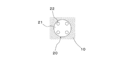
接点部20は、金属体であって例えば電鋳によってフレキシブル基板10上に複数(多数)設けられ、検査時に検査対象デバイス7のバンプ(電極)8と接触する。図3及び図4(A),(B)に示すように、接点部20は、本体部21と、接触用凸部22と、位置合わせ用凸部(脚部)23と、を有する。本体部21は、円柱形状であって上下端部にそれぞれ鍔部21aを有し、鍔部21a間にフレキシブル基板10を挟み込んでいる。フレキシブル基板10の上面側において、接触用凸部22は、本体部21の上面側の鍔部21aの上面から例えば円柱状に上方に突出し、図6に示すように1つの接点部20につき例えば4つ設けられる。フレキシブル基板10の下面側において、位置合わせ用凸部23は、図3に示すように本体部21の下面側の鍔部21aの下面中心部から例えば円柱状に下方に突出し、図4(A),(B)に示すようにスプリング30の内側に延びる(入り込む)。位置合わせ用凸部23は、コンタクタ1の組立時に接点部20及びスプリング30の相互の位置合わせに用いられると共に、スプリング30との係合(例えば軽圧入)により、スプリング30からの接点部20の抜けを防止する抜止め力を発生する。
The
スプリング30は、接点部20と同数設けられた導電性材料からなるコイルスプリングであり、各々の接点部20を検査対象物側に向けて付勢する。スプリング30が接点部20を下方から支持することで、フレキシブル基板10が、ハウジング40のフレキシブル基板10が配置される面から浮いた状態で支持される。フレキシブル基板10は、ハウジング40に対して固定的には支持されない。図4(A),(B)に示すように、各々のスプリング30は、両端部にそれぞれ平坦巻き部31を有し、かつ自身の長さ方向の中間部に斜め密着巻き部32を有する。上端側の平坦巻き部31の内側に、接点部20の位置合わせ用凸部23が嵌入(軽圧入)される。各々のスプリング30の開放状態において、図4(A)に示すように、平坦巻き部31と斜め密着巻き部32との間に隙間Gが存在する。具体的には、各々のスプリング30において平坦巻き部31と斜め密着巻き部32との間を渡す連絡部33は、スプリング30の開放時に斜め密着巻き部32よりも傾斜が急となっており、これにより前述の隙間Gが形成される。一方、各々のスプリング30が所定長圧縮されると、図4(B)に示すように、隙間Gが無くなって平坦巻き部31と斜め密着巻き部32とが相互に接触する。なお、スプリング30の平坦巻き部31を斜め密着巻き部32と比較して小径としている目的は、平坦巻き部31が接点部20の位置合わせ用凸部23の圧入により膨らんでもハウジング40の貫通穴41内に確実に収まること、及び平坦巻き部31が検査用基板5の図示しない電極からはみ出さすことの防止である。
The
ハウジング40は、例えば絶縁樹脂製であり、各々のスプリング30を収容する。具体的には、ハウジング40は、スプリング30と同数の貫通穴41を有し、各々の貫通穴41にスプリング30を1つずつ収容する。ハウジング40は、フレキシブル基板10を貫通してフレキシブル基板10の下面側から上面側に延びる複数の(ここでは4つの)ストッパ凸部(ハードストップ)42を有する。ストッパ凸部42は、図2に示すように、検査時における検査対象デバイス7の下限位置を定める。検査対象デバイス7が下降してストッパ凸部42の上面に接触して検査時の状態に移行するまでの間に、スプリング30の図4(A)に示す隙間Gが無くなるような寸法設計となっている。
The
ガイド50は、例えば絶縁樹脂製であり、検査時に検査対象デバイス7の前後左右方向の位置を定め、検査対象デバイス7を上下方向に移動可能に支持するガイド穴51を有する。ハウジング40及びガイド50は、不図示のネジ等によって相互に固定される。位置決めピン60は、下端側がハウジング40に圧入等により固定され、上端側がガイド50に圧入等により固定され、ハウジング40及びガイド50の間の空間においてフレキシブル基板10のピン挿通穴11を貫通する。
The
コンタクタ1の組立ては、例えば以下の手順による。まず、ハウジング40の各々の貫通穴41に、スプリング30を挿入すると共に、位置決めピン60をハウジング40に圧入固定する。一方、フレキシブル基板10には電鋳等により多数の接点部20を一括形成しておき、そのフレキシブル基板10を、ピン挿通穴11に位置決めピン60を通しながらスプリング30上に配置し、接点部20の位置合わせ用凸部23を、スプリング30の上端部の平坦巻き部31の内側に入り込ませる(嵌め込む)。続いて、ガイド50をハウジング40上にネジ止め等により固定する。
The assembly of the
コンタクタ1による検査は、例えば以下の手順による。コンタクタ1は検査用基板5上にネジ止め等により固定しておく。そして、図1に示すように検査対象デバイス7をガイド50のガイド穴51に挿入し、図2に示すように検査対象デバイス7を接点部20に向けて押し付けていく。すると、検査対象デバイス7のバンプ8が接点部20に接触し、接点部20がスプリング30の付勢力に抗して後退(下降)する。これにより、バンプ8と接点部20との間に必要十分な接触力が得られ、この状態で検査対象デバイス7の検査が行われる。
The inspection by the
本実施の形態によれば、下記の効果を奏することができる。 According to the present embodiment, the following effects can be achieved.
(1) 接点部20を例えば電鋳技術によりフレキシブル基板10に多数個一括して形成することができるため、ハウジング40の貫通穴41にプランジャを個別に挿入する作業が不要となり、製造容易で工数が掛からず、コスト安である。
(1) Since a large number of
(2) 接点部20をスプリング30により付勢する構成であり、特許文献2のように弾性を有する金属線埋設シートで接点部を支持する構成と比較してストロークを長く確保できるため、検査対象デバイス7のバンプ8のコプラナリティがバラついても安定したコンタクトが得られる。
(2) Since the
(3) 特許文献2において金属線埋設シートを構成するシリコーンゴムシートは高温、低温で硬度が変化するために、高温、低温の環境下では押し圧が変化して安定したコンタクトが得られないという問題があるが、本実施の形態ではスプリング30による付勢のため高温、低温の環境下でも安定した押し圧が得られ、コンタクトの安定性が高い。また、特許文献2の構成と異なりゴムのへたりによる寿命の問題がなく、多数回の使用に耐えられる。
(3) The hardness of the silicone rubber sheet constituting the metal wire embedded sheet in Patent Document 2 changes at high temperature and low temperature, so that the pressing pressure changes in a high temperature and low temperature environment, and a stable contact can not be obtained. Although there is a problem, in the present embodiment, a stable pressing pressure can be obtained even in high temperature and low temperature environments due to the biasing by the
(4) スプリング30は、接点部20と係合する上端部が平坦巻き部31となっており、スプリング30による付勢により接点部20の平坦度の悪化を抑制できる。一方、スプリング30は、自身の長さ方向の中間部が斜め密着巻き部32となっており、ストローク長を確保しながら電流経路(電気長)を短くすることができる。ここで、スプリング30の開放状態において図4(A)に示すように平坦巻き部31と斜め密着巻き部32との間に隙間Gが存在するため、隙間Gが存在しない場合と比較して更にストロークを長く確保できる。なお、図4(B)に示す検査時にはスプリング30の圧縮により隙間Gは無くなっており、隙間Gにより電気長が長くなるという問題もない。密着巻き部を通して電気信号を伝達することで、電気長が短くなり、検査対象デバイス7の高速信号を検査用基板5に高品質に伝送できる。
(4) The upper end portion of the
以上、実施の形態を例に本発明を説明したが、実施の形態の各構成要素や各処理プロセスには請求項に記載の範囲で種々の変形が可能であることは当業者に理解されるところである。以下、変形例について触れる。 Although the present invention has been described above by taking the embodiment as an example, it is understood by those skilled in the art that various modifications can be made to each component and each processing process of the embodiment within the scope of the claims. It is a place. The following describes the modification.
フレキシブル基板10の貫通穴13、接点部20、接触用凸部22、スプリング30、平坦巻き部31の巻数、ストッパ凸部42、及び位置決めピン60等の個数は、実施の形態で示した具体的な数値に限定されず、個々の製品の設計上の要求や都合に合わせて適宜設定すればよい。なお、平坦巻き部31は、複数回巻きとする場合、少なくともスプリング30の圧縮時(検査時)には相互に密着することが望ましい。
The numbers of the through
要求される仕様によっては、スプリング30に斜め密着巻き部32あるいは平坦巻き部31を設けない構成、平坦巻き部31と斜め密着巻き部32との間に隙間Gを設けない構成、フレキシブル基板10に貫通穴13を設けない構成、ハウジング40にストッパ凸部42を設けない構成、接点部20に接触用凸部22や位置合わせ用凸部23を設けない構成等も可能である。
Depending on the required specifications, the
1 コンタクタ、5 検査用基板、7 検査対象デバイス、8 バンプ(電極)、
10 フレキシブル基板、11 ピン挿通穴、12 ストッパ用穴、13 貫通穴、
20 接点部、21 本体部、21a 鍔部、22 接触用凸部、23 位置合わせ用凸部(脚部)、
30 スプリング、31 平坦巻き部、32 斜め密着巻き部、33 連絡部、
40 ハウジング、41 貫通穴、42 ストッパ凸部、
50 ガイド、51 ガイド穴、60 位置決めピン、G 隙間
1 contactor, 5 inspection substrates, 7 inspection target devices, 8 bumps (electrodes),
10 flexible substrate, 11 pin insertion holes, 12 stopper holes, 13 through holes,
20 contact portion, 21 main body portion, 21a ridge portion, 22 contact convex portion, 23 alignment convex portion (leg portion)
30 springs, 31 flat wound parts, 32 diagonal close wound parts, 33 contact parts,
40 housing, 41 through hole, 42 stopper projection,
50 Guide, 51 Guide Hole, 60 Positioning Pin, G Clearance
Claims (10)
各々のスプリングは、少なくとも前記接点部側の端部に平坦巻き部を有する、コンタクタ。 A flexible substrate, a plurality of contact portions provided on the flexible substrate, a plurality of springs urging the respective contact portions toward the object, and a housing accommodating the plurality of springs.
Each spring has a flat winding portion at an end portion of at least the contact portion, the contactor.
各々のスプリングは、自身の長さ方向の中間部に斜め密着巻き部を有する、コンタクタ。 A flexible substrate, a plurality of contact portions provided on the flexible substrate, a plurality of springs urging the respective contact portions toward the object, and a housing accommodating the plurality of springs.
Each of the springs has a diagonal close wound portion at the middle in the longitudinal direction of the contactor.
各々のスプリングは、少なくとも前記接点部側の端部に平坦巻き部を有し、かつ自身の長さ方向の中間部に斜め密着巻き部を有し、開放状態において前記平坦巻き部と前記斜め密着巻き部との間に隙間が存在する、コンタクタ。 A flexible substrate, a plurality of contact portions provided on the flexible substrate, a plurality of springs urging the respective contact portions toward the object, and a housing accommodating the plurality of springs.
Each spring has a flat winding portion at least at an end portion on the contact portion side, and an oblique close winding portion at an intermediate portion in the length direction of the spring, and in the open state, the flat winding portion and the oblique contact There is a gap between the winding part , contactor.
各々の接点部は、前記スプリングの内側に延びる位置合わせ用凸部を有する、コンタクタ。 A flexible substrate, a plurality of contact portions provided on the flexible substrate, a plurality of springs urging the respective contact portions toward the object, and a housing accommodating the plurality of springs.
Contact portions of each having a positioning projection extending inwardly of the spring, contactor.
前記ハウジングは、前記フレキシブル基板を貫通して前記フレキシブル基板の一面側から他面側に延びるストッパ凸部を有する、コンタクタ。 A flexible substrate, a plurality of contact portions provided on the flexible substrate, a plurality of springs urging the respective contact portions toward the object, and a housing accommodating the plurality of springs.
The said housing is a contactor which has the stopper convex part which penetrates the said flexible substrate and extends from the one surface side of the said flexible substrate to the other surface side.
前記フレキシブル基板は、各々の接点部の周囲に、前記接点部の接触先の高低差による自身の撓みを防止するための貫通穴を有する、コンタクタ。 A flexible substrate, a plurality of contact portions provided on the flexible substrate, a plurality of springs urging the respective contact portions toward the object, and a housing accommodating the plurality of springs.
The said flexible substrate is a contactor which has a through-hole for preventing own bending by the height difference of the contact destination of the said contact part around each contact part.
Priority Applications (4)
| Application Number | Priority Date | Filing Date | Title |
|---|---|---|---|
| JP2015194768A JP6553472B2 (en) | 2015-09-30 | 2015-09-30 | Contactor |
| US15/762,881 US10317430B2 (en) | 2015-09-30 | 2016-09-06 | Contactor with a plurality of springs and contact point portions urged by the springs |
| PCT/JP2016/076208 WO2017056879A1 (en) | 2015-09-30 | 2016-09-06 | Contactor |
| TW105131583A TWI677686B (en) | 2015-09-30 | 2016-09-30 | Contactor |
Applications Claiming Priority (1)
| Application Number | Priority Date | Filing Date | Title |
|---|---|---|---|
| JP2015194768A JP6553472B2 (en) | 2015-09-30 | 2015-09-30 | Contactor |
Publications (3)
| Publication Number | Publication Date |
|---|---|
| JP2017067662A JP2017067662A (en) | 2017-04-06 |
| JP2017067662A5 JP2017067662A5 (en) | 2018-10-11 |
| JP6553472B2 true JP6553472B2 (en) | 2019-07-31 |
Family
ID=58423420
Family Applications (1)
| Application Number | Title | Priority Date | Filing Date |
|---|---|---|---|
| JP2015194768A Active JP6553472B2 (en) | 2015-09-30 | 2015-09-30 | Contactor |
Country Status (4)
| Country | Link |
|---|---|
| US (1) | US10317430B2 (en) |
| JP (1) | JP6553472B2 (en) |
| TW (1) | TWI677686B (en) |
| WO (1) | WO2017056879A1 (en) |
Families Citing this family (7)
| Publication number | Priority date | Publication date | Assignee | Title |
|---|---|---|---|---|
| CN207424024U (en) * | 2017-11-23 | 2018-05-29 | 周婷 | The elastomer structure of conducting probe |
| US10931058B2 (en) * | 2018-09-24 | 2021-02-23 | Apple Inc. | Gaskets for sealing spring-loaded contacts |
| KR20220027188A (en) * | 2019-09-30 | 2022-03-07 | 미쓰비시덴키 가부시키가이샤 | inspection jig |
| KR102080832B1 (en) * | 2019-10-02 | 2020-02-24 | 황동원 | Spring contact and test socket with the spring contact |
| US11831093B2 (en) * | 2021-03-30 | 2023-11-28 | Cisco Technology, Inc. | Socket locator |
| US11714105B2 (en) * | 2021-03-30 | 2023-08-01 | Enplas Corporation | Socket and inspection socket |
| US20230180379A1 (en) * | 2021-12-03 | 2023-06-08 | Xilinx, Inc. | Micro device with adaptable thermal management device |
Family Cites Families (25)
| Publication number | Priority date | Publication date | Assignee | Title |
|---|---|---|---|---|
| US5399982A (en) * | 1989-11-13 | 1995-03-21 | Mania Gmbh & Co. | Printed circuit board testing device with foil adapter |
| JPH0540131A (en) * | 1991-08-06 | 1993-02-19 | Nec Corp | Testing jig |
| JP3653131B2 (en) * | 1995-12-28 | 2005-05-25 | 日本発条株式会社 | Conductive contact |
| JP3634074B2 (en) * | 1996-06-28 | 2005-03-30 | 日本発条株式会社 | Conductive contact |
| US5955888A (en) * | 1997-09-10 | 1999-09-21 | Xilinx, Inc. | Apparatus and method for testing ball grid array packaged integrated circuits |
| US6900651B1 (en) * | 1998-07-10 | 2005-05-31 | Nhk Spring Co., Ltd. | Electroconductive contact unit assembly |
| JP4167202B2 (en) * | 1998-07-10 | 2008-10-15 | 日本発条株式会社 | Conductive contact |
| JP2000180506A (en) | 1998-12-15 | 2000-06-30 | Nec Corp | Contact device for inspecting semiconductor device |
| JP3527724B2 (en) * | 1999-11-17 | 2004-05-17 | 株式会社アドバンテスト | IC socket and IC test equipment |
| US7254889B1 (en) * | 2000-09-08 | 2007-08-14 | Gabe Cherian | Interconnection devices |
| US6685492B2 (en) * | 2001-12-27 | 2004-02-03 | Rika Electronics International, Inc. | Sockets for testing electronic packages having contact probes with contact tips easily maintainable in optimum operational condition |
| US20100167561A1 (en) * | 2003-04-11 | 2010-07-01 | Neoconix, Inc. | Structure and process for a contact grid array formed in a circuitized substrate |
| JP4242199B2 (en) * | 2003-04-25 | 2009-03-18 | 株式会社ヨコオ | IC socket |
| JP4271133B2 (en) * | 2004-12-10 | 2009-06-03 | アルプス電気株式会社 | Relay board |
| US20070018666A1 (en) * | 2005-07-22 | 2007-01-25 | Nasser Barabi | Spring contact pin for an IC chip tester |
| JP2007078456A (en) * | 2005-09-13 | 2007-03-29 | Yokogawa Electric Corp | Ic socket and ic tester using the same |
| JP4842640B2 (en) | 2005-12-28 | 2011-12-21 | 日本発條株式会社 | Probe card and inspection method |
| CN101109768A (en) * | 2006-07-17 | 2008-01-23 | 范伟芳 | Improved structure of modularized elastic probe |
| JP4832213B2 (en) * | 2006-08-18 | 2011-12-07 | 株式会社ヨコオ | probe |
| JP2009094006A (en) * | 2007-10-11 | 2009-04-30 | Enplas Corp | Fitting structure of electrical component socket |
| JP5008582B2 (en) | 2008-02-04 | 2012-08-22 | 株式会社ヨコオ | Contact probe |
| US8808037B2 (en) * | 2009-10-12 | 2014-08-19 | Iwin Co., Ltd. | Slidable pogo pin |
| JP5960383B2 (en) * | 2010-06-01 | 2016-08-02 | スリーエム イノベイティブ プロパティズ カンパニー | Contact holder |
| US8506307B2 (en) * | 2010-12-02 | 2013-08-13 | Interconnect Devices, Inc. | Electrical connector with embedded shell layer |
| WO2013018809A1 (en) * | 2011-08-02 | 2013-02-07 | 日本発條株式会社 | Probe unit |
-
2015
- 2015-09-30 JP JP2015194768A patent/JP6553472B2/en active Active
-
2016
- 2016-09-06 WO PCT/JP2016/076208 patent/WO2017056879A1/en active Application Filing
- 2016-09-06 US US15/762,881 patent/US10317430B2/en not_active Expired - Fee Related
- 2016-09-30 TW TW105131583A patent/TWI677686B/en not_active IP Right Cessation
Also Published As
| Publication number | Publication date |
|---|---|
| TW201719176A (en) | 2017-06-01 |
| US10317430B2 (en) | 2019-06-11 |
| WO2017056879A1 (en) | 2017-04-06 |
| TWI677686B (en) | 2019-11-21 |
| US20180275167A1 (en) | 2018-09-27 |
| JP2017067662A (en) | 2017-04-06 |
Similar Documents
| Publication | Publication Date | Title |
|---|---|---|
| JP6553472B2 (en) | Contactor | |
| US8669774B2 (en) | Probe pin and an IC socket with the same | |
| KR101894965B1 (en) | Probe pin and ic socket | |
| US8324919B2 (en) | Scrub inducing compliant electrical contact | |
| WO2011096067A1 (en) | Contact and electrical connection device | |
| JP7095753B2 (en) | probe | |
| KR102033135B1 (en) | A probe pin | |
| KR101330198B1 (en) | Probe apparatus for test and fabrication method thereof | |
| KR20070005520A (en) | Socket for inspection apparatus | |
| JP6328925B2 (en) | Contact probe and socket for electrical parts | |
| JP2013140058A (en) | Probe pin and socket for electric component | |
| KR101641923B1 (en) | A contact probe | |
| KR101236312B1 (en) | Probe for testing semiconductor | |
| KR101471652B1 (en) | Insert and Apparatus for testing semiconductor package including the same | |
| JP6211861B2 (en) | Contact pin and socket for electrical parts | |
| KR20170000572A (en) | Probe apparatus for test of electronic device | |
| JP2017142138A (en) | Probe pin and anisotropic conductive member | |
| KR102170384B1 (en) | Pogo pin with extended contact tolerance using a MEMS plunger | |
| JP2013195282A (en) | Contact probe, semiconductor element socket provided with contact probe, and method for manufacturing contact probe | |
| JP6372997B2 (en) | Socket for electrical parts | |
| KR101626513B1 (en) | Semiconductor chip test socket | |
| JP7113067B2 (en) | Contact probe and test socket with it | |
| WO2015163160A1 (en) | Probe pin and ic socket | |
| KR20180025711A (en) | A fineness-double probe pin | |
| JP2008077988A (en) | Contact terminal and socket for semiconductor device equipped with it |
Legal Events
| Date | Code | Title | Description |
|---|---|---|---|
| A521 | Request for written amendment filed |
Free format text: JAPANESE INTERMEDIATE CODE: A523 Effective date: 20180829 |
|
| A621 | Written request for application examination |
Free format text: JAPANESE INTERMEDIATE CODE: A621 Effective date: 20180829 |
|
| TRDD | Decision of grant or rejection written | ||
| A01 | Written decision to grant a patent or to grant a registration (utility model) |
Free format text: JAPANESE INTERMEDIATE CODE: A01 Effective date: 20190618 |
|
| A61 | First payment of annual fees (during grant procedure) |
Free format text: JAPANESE INTERMEDIATE CODE: A61 Effective date: 20190704 |
|
| R150 | Certificate of patent or registration of utility model |
Ref document number: 6553472 Country of ref document: JP Free format text: JAPANESE INTERMEDIATE CODE: R150 |
|
| R250 | Receipt of annual fees |
Free format text: JAPANESE INTERMEDIATE CODE: R250 |
|
| R250 | Receipt of annual fees |
Free format text: JAPANESE INTERMEDIATE CODE: R250 |