JP6528366B2 - Method of manufacturing vertical trench MOSFET - Google Patents
Method of manufacturing vertical trench MOSFET Download PDFInfo
- Publication number
- JP6528366B2 JP6528366B2 JP2014140520A JP2014140520A JP6528366B2 JP 6528366 B2 JP6528366 B2 JP 6528366B2 JP 2014140520 A JP2014140520 A JP 2014140520A JP 2014140520 A JP2014140520 A JP 2014140520A JP 6528366 B2 JP6528366 B2 JP 6528366B2
- Authority
- JP
- Japan
- Prior art keywords
- insulating film
- gate insulating
- semiconductor layer
- gate
- manufacturing
- Prior art date
- Legal status (The legal status is an assumption and is not a legal conclusion. Google has not performed a legal analysis and makes no representation as to the accuracy of the status listed.)
- Active
Links
- 238000004519 manufacturing process Methods 0.000 title claims description 40
- 239000004065 semiconductor Substances 0.000 claims description 277
- 238000000034 method Methods 0.000 claims description 82
- 230000008569 process Effects 0.000 claims description 63
- 238000000231 atomic layer deposition Methods 0.000 claims description 58
- 238000000137 annealing Methods 0.000 claims description 50
- 239000007800 oxidant agent Substances 0.000 claims description 38
- CBENFWSGALASAD-UHFFFAOYSA-N Ozone Chemical compound [O-][O+]=O CBENFWSGALASAD-UHFFFAOYSA-N 0.000 claims description 33
- OKTJSMMVPCPJKN-UHFFFAOYSA-N Carbon Chemical compound [C] OKTJSMMVPCPJKN-UHFFFAOYSA-N 0.000 claims description 30
- 229910052799 carbon Inorganic materials 0.000 claims description 30
- JMASRVWKEDWRBT-UHFFFAOYSA-N Gallium nitride Chemical compound [Ga]#N JMASRVWKEDWRBT-UHFFFAOYSA-N 0.000 claims description 28
- QVGXLLKOCUKJST-UHFFFAOYSA-N atomic oxygen Chemical compound [O] QVGXLLKOCUKJST-UHFFFAOYSA-N 0.000 claims description 28
- 239000001301 oxygen Substances 0.000 claims description 28
- 229910052760 oxygen Inorganic materials 0.000 claims description 28
- 230000001590 oxidative effect Effects 0.000 claims description 21
- 230000009467 reduction Effects 0.000 claims description 15
- 239000007789 gas Substances 0.000 claims description 12
- WGTYBPLFGIVFAS-UHFFFAOYSA-M tetramethylammonium hydroxide Chemical compound [OH-].C[N+](C)(C)C WGTYBPLFGIVFAS-UHFFFAOYSA-M 0.000 claims description 12
- 238000001312 dry etching Methods 0.000 claims description 11
- 238000010926 purge Methods 0.000 claims description 11
- 239000002994 raw material Substances 0.000 claims description 11
- 238000001039 wet etching Methods 0.000 claims description 9
- UFHFLCQGNIYNRP-UHFFFAOYSA-N Hydrogen Chemical compound [H][H] UFHFLCQGNIYNRP-UHFFFAOYSA-N 0.000 claims description 8
- 239000001257 hydrogen Substances 0.000 claims description 8
- 229910052739 hydrogen Inorganic materials 0.000 claims description 8
- 238000011156 evaluation Methods 0.000 description 31
- 239000000758 substrate Substances 0.000 description 30
- VYPSYNLAJGMNEJ-UHFFFAOYSA-N Silicium dioxide Chemical compound O=[Si]=O VYPSYNLAJGMNEJ-UHFFFAOYSA-N 0.000 description 20
- 230000015572 biosynthetic process Effects 0.000 description 12
- 238000010438 heat treatment Methods 0.000 description 12
- 239000010936 titanium Substances 0.000 description 12
- XUIMIQQOPSSXEZ-UHFFFAOYSA-N Silicon Chemical compound [Si] XUIMIQQOPSSXEZ-UHFFFAOYSA-N 0.000 description 11
- 229910052710 silicon Inorganic materials 0.000 description 11
- 239000010703 silicon Substances 0.000 description 11
- 229910004298 SiO 2 Inorganic materials 0.000 description 10
- 230000006872 improvement Effects 0.000 description 10
- 239000000377 silicon dioxide Substances 0.000 description 10
- 235000012239 silicon dioxide Nutrition 0.000 description 10
- 229910052782 aluminium Inorganic materials 0.000 description 9
- XAGFODPZIPBFFR-UHFFFAOYSA-N aluminium Chemical compound [Al] XAGFODPZIPBFFR-UHFFFAOYSA-N 0.000 description 9
- 238000010030 laminating Methods 0.000 description 9
- 229910002601 GaN Inorganic materials 0.000 description 8
- 238000005530 etching Methods 0.000 description 8
- 239000011777 magnesium Substances 0.000 description 8
- KDLHZDBZIXYQEI-UHFFFAOYSA-N Palladium Chemical compound [Pd] KDLHZDBZIXYQEI-UHFFFAOYSA-N 0.000 description 6
- RTAQQCXQSZGOHL-UHFFFAOYSA-N Titanium Chemical compound [Ti] RTAQQCXQSZGOHL-UHFFFAOYSA-N 0.000 description 6
- 230000006866 deterioration Effects 0.000 description 6
- 238000000921 elemental analysis Methods 0.000 description 6
- 238000005468 ion implantation Methods 0.000 description 6
- 239000000463 material Substances 0.000 description 6
- 229910052719 titanium Inorganic materials 0.000 description 6
- 230000015556 catabolic process Effects 0.000 description 5
- FYYHWMGAXLPEAU-UHFFFAOYSA-N Magnesium Chemical compound [Mg] FYYHWMGAXLPEAU-UHFFFAOYSA-N 0.000 description 4
- 238000005275 alloying Methods 0.000 description 4
- 230000003247 decreasing effect Effects 0.000 description 4
- 230000000994 depressogenic effect Effects 0.000 description 4
- 239000010931 gold Substances 0.000 description 4
- 229910052749 magnesium Inorganic materials 0.000 description 4
- TWNQGVIAIRXVLR-UHFFFAOYSA-N oxo(oxoalumanyloxy)alumane Chemical compound O=[Al]O[Al]=O TWNQGVIAIRXVLR-UHFFFAOYSA-N 0.000 description 4
- 229910018072 Al 2 O 3 Inorganic materials 0.000 description 3
- 239000000956 alloy Substances 0.000 description 3
- 229910045601 alloy Inorganic materials 0.000 description 3
- 238000000151 deposition Methods 0.000 description 3
- 230000008021 deposition Effects 0.000 description 3
- 238000010292 electrical insulation Methods 0.000 description 3
- CJNBYAVZURUTKZ-UHFFFAOYSA-N hafnium(iv) oxide Chemical compound O=[Hf]=O CJNBYAVZURUTKZ-UHFFFAOYSA-N 0.000 description 3
- RVTZCBVAJQQJTK-UHFFFAOYSA-N oxygen(2-);zirconium(4+) Chemical compound [O-2].[O-2].[Zr+4] RVTZCBVAJQQJTK-UHFFFAOYSA-N 0.000 description 3
- 230000000149 penetrating effect Effects 0.000 description 3
- 229910001928 zirconium oxide Inorganic materials 0.000 description 3
- 230000005669 field effect Effects 0.000 description 2
- PCHJSUWPFVWCPO-UHFFFAOYSA-N gold Chemical compound [Au] PCHJSUWPFVWCPO-UHFFFAOYSA-N 0.000 description 2
- 229910052737 gold Inorganic materials 0.000 description 2
- 238000004050 hot filament vapor deposition Methods 0.000 description 2
- 238000009616 inductively coupled plasma Methods 0.000 description 2
- 238000009413 insulation Methods 0.000 description 2
- 238000012986 modification Methods 0.000 description 2
- 230000004048 modification Effects 0.000 description 2
- 150000004767 nitrides Chemical class 0.000 description 2
- 229910052763 palladium Inorganic materials 0.000 description 2
- 238000001004 secondary ion mass spectrometry Methods 0.000 description 2
- 238000004544 sputter deposition Methods 0.000 description 2
- 229910017109 AlON Inorganic materials 0.000 description 1
- PIGFYZPCRLYGLF-UHFFFAOYSA-N Aluminum nitride Chemical compound [Al]#N PIGFYZPCRLYGLF-UHFFFAOYSA-N 0.000 description 1
- 229910052581 Si3N4 Inorganic materials 0.000 description 1
- 229910006252 ZrON Inorganic materials 0.000 description 1
- 239000012298 atmosphere Substances 0.000 description 1
- 239000000969 carrier Substances 0.000 description 1
- PMHQVHHXPFUNSP-UHFFFAOYSA-M copper(1+);methylsulfanylmethane;bromide Chemical compound Br[Cu].CSC PMHQVHHXPFUNSP-UHFFFAOYSA-M 0.000 description 1
- 239000013078 crystal Substances 0.000 description 1
- 238000009792 diffusion process Methods 0.000 description 1
- 230000000694 effects Effects 0.000 description 1
- 229910052732 germanium Inorganic materials 0.000 description 1
- GNPVGFCGXDBREM-UHFFFAOYSA-N germanium atom Chemical compound [Ge] GNPVGFCGXDBREM-UHFFFAOYSA-N 0.000 description 1
- 239000012535 impurity Substances 0.000 description 1
- 239000012528 membrane Substances 0.000 description 1
- 239000000203 mixture Substances 0.000 description 1
- 238000005268 plasma chemical vapour deposition Methods 0.000 description 1
- 238000001020 plasma etching Methods 0.000 description 1
- 238000000623 plasma-assisted chemical vapour deposition Methods 0.000 description 1
- HBMJWWWQQXIZIP-UHFFFAOYSA-N silicon carbide Chemical compound [Si+]#[C-] HBMJWWWQQXIZIP-UHFFFAOYSA-N 0.000 description 1
- HQVNEWCFYHHQES-UHFFFAOYSA-N silicon nitride Chemical compound N12[Si]34N5[Si]62N3[Si]51N64 HQVNEWCFYHHQES-UHFFFAOYSA-N 0.000 description 1
- 229910052814 silicon oxide Inorganic materials 0.000 description 1
- JBQYATWDVHIOAR-UHFFFAOYSA-N tellanylidenegermanium Chemical compound [Te]=[Ge] JBQYATWDVHIOAR-UHFFFAOYSA-N 0.000 description 1
Images


Classifications
-
- H—ELECTRICITY
- H01—ELECTRIC ELEMENTS
- H01L—SEMICONDUCTOR DEVICES NOT COVERED BY CLASS H10
- H01L29/00—Semiconductor devices adapted for rectifying, amplifying, oscillating or switching, or capacitors or resistors with at least one potential-jump barrier or surface barrier, e.g. PN junction depletion layer or carrier concentration layer; Details of semiconductor bodies or of electrodes thereof ; Multistep manufacturing processes therefor
- H01L29/66—Types of semiconductor device ; Multistep manufacturing processes therefor
- H01L29/68—Types of semiconductor device ; Multistep manufacturing processes therefor controllable by only the electric current supplied, or only the electric potential applied, to an electrode which does not carry the current to be rectified, amplified or switched
- H01L29/76—Unipolar devices, e.g. field effect transistors
- H01L29/772—Field effect transistors
- H01L29/78—Field effect transistors with field effect produced by an insulated gate
-
- H—ELECTRICITY
- H01—ELECTRIC ELEMENTS
- H01L—SEMICONDUCTOR DEVICES NOT COVERED BY CLASS H10
- H01L21/00—Processes or apparatus adapted for the manufacture or treatment of semiconductor or solid state devices or of parts thereof
- H01L21/02—Manufacture or treatment of semiconductor devices or of parts thereof
- H01L21/02104—Forming layers
- H01L21/02107—Forming insulating materials on a substrate
- H01L21/02109—Forming insulating materials on a substrate characterised by the type of layer, e.g. type of material, porous/non-porous, pre-cursors, mixtures or laminates
- H01L21/02112—Forming insulating materials on a substrate characterised by the type of layer, e.g. type of material, porous/non-porous, pre-cursors, mixtures or laminates characterised by the material of the layer
- H01L21/02123—Forming insulating materials on a substrate characterised by the type of layer, e.g. type of material, porous/non-porous, pre-cursors, mixtures or laminates characterised by the material of the layer the material containing silicon
- H01L21/02126—Forming insulating materials on a substrate characterised by the type of layer, e.g. type of material, porous/non-porous, pre-cursors, mixtures or laminates characterised by the material of the layer the material containing silicon the material containing Si, O, and at least one of H, N, C, F, or other non-metal elements, e.g. SiOC, SiOC:H or SiONC
-
- H—ELECTRICITY
- H01—ELECTRIC ELEMENTS
- H01L—SEMICONDUCTOR DEVICES NOT COVERED BY CLASS H10
- H01L21/00—Processes or apparatus adapted for the manufacture or treatment of semiconductor or solid state devices or of parts thereof
- H01L21/02—Manufacture or treatment of semiconductor devices or of parts thereof
- H01L21/02104—Forming layers
- H01L21/02107—Forming insulating materials on a substrate
- H01L21/02109—Forming insulating materials on a substrate characterised by the type of layer, e.g. type of material, porous/non-porous, pre-cursors, mixtures or laminates
- H01L21/022—Forming insulating materials on a substrate characterised by the type of layer, e.g. type of material, porous/non-porous, pre-cursors, mixtures or laminates the layer being a laminate, i.e. composed of sublayers, e.g. stacks of alternating high-k metal oxides
-
- H—ELECTRICITY
- H01—ELECTRIC ELEMENTS
- H01L—SEMICONDUCTOR DEVICES NOT COVERED BY CLASS H10
- H01L21/00—Processes or apparatus adapted for the manufacture or treatment of semiconductor or solid state devices or of parts thereof
- H01L21/02—Manufacture or treatment of semiconductor devices or of parts thereof
- H01L21/02104—Forming layers
- H01L21/02107—Forming insulating materials on a substrate
- H01L21/02225—Forming insulating materials on a substrate characterised by the process for the formation of the insulating layer
- H01L21/0226—Forming insulating materials on a substrate characterised by the process for the formation of the insulating layer formation by a deposition process
- H01L21/02263—Forming insulating materials on a substrate characterised by the process for the formation of the insulating layer formation by a deposition process deposition from the gas or vapour phase
- H01L21/02271—Forming insulating materials on a substrate characterised by the process for the formation of the insulating layer formation by a deposition process deposition from the gas or vapour phase deposition by decomposition or reaction of gaseous or vapour phase compounds, i.e. chemical vapour deposition
- H01L21/02274—Forming insulating materials on a substrate characterised by the process for the formation of the insulating layer formation by a deposition process deposition from the gas or vapour phase deposition by decomposition or reaction of gaseous or vapour phase compounds, i.e. chemical vapour deposition in the presence of a plasma [PECVD]
-
- H—ELECTRICITY
- H01—ELECTRIC ELEMENTS
- H01L—SEMICONDUCTOR DEVICES NOT COVERED BY CLASS H10
- H01L21/00—Processes or apparatus adapted for the manufacture or treatment of semiconductor or solid state devices or of parts thereof
- H01L21/02—Manufacture or treatment of semiconductor devices or of parts thereof
- H01L21/02104—Forming layers
- H01L21/02107—Forming insulating materials on a substrate
- H01L21/02225—Forming insulating materials on a substrate characterised by the process for the formation of the insulating layer
- H01L21/0226—Forming insulating materials on a substrate characterised by the process for the formation of the insulating layer formation by a deposition process
- H01L21/02263—Forming insulating materials on a substrate characterised by the process for the formation of the insulating layer formation by a deposition process deposition from the gas or vapour phase
- H01L21/02271—Forming insulating materials on a substrate characterised by the process for the formation of the insulating layer formation by a deposition process deposition from the gas or vapour phase deposition by decomposition or reaction of gaseous or vapour phase compounds, i.e. chemical vapour deposition
- H01L21/0228—Forming insulating materials on a substrate characterised by the process for the formation of the insulating layer formation by a deposition process deposition from the gas or vapour phase deposition by decomposition or reaction of gaseous or vapour phase compounds, i.e. chemical vapour deposition deposition by cyclic CVD, e.g. ALD, ALE, pulsed CVD
-
- H—ELECTRICITY
- H01—ELECTRIC ELEMENTS
- H01L—SEMICONDUCTOR DEVICES NOT COVERED BY CLASS H10
- H01L21/00—Processes or apparatus adapted for the manufacture or treatment of semiconductor or solid state devices or of parts thereof
- H01L21/02—Manufacture or treatment of semiconductor devices or of parts thereof
- H01L21/04—Manufacture or treatment of semiconductor devices or of parts thereof the devices having at least one potential-jump barrier or surface barrier, e.g. PN junction, depletion layer or carrier concentration layer
- H01L21/18—Manufacture or treatment of semiconductor devices or of parts thereof the devices having at least one potential-jump barrier or surface barrier, e.g. PN junction, depletion layer or carrier concentration layer the devices having semiconductor bodies comprising elements of Group IV of the Periodic System or AIIIBV compounds with or without impurities, e.g. doping materials
- H01L21/28—Manufacture of electrodes on semiconductor bodies using processes or apparatus not provided for in groups H01L21/20 - H01L21/268
- H01L21/28008—Making conductor-insulator-semiconductor electrodes
- H01L21/28264—Making conductor-insulator-semiconductor electrodes the insulator being formed after the semiconductor body, the semiconductor being a III-V compound
-
- H—ELECTRICITY
- H01—ELECTRIC ELEMENTS
- H01L—SEMICONDUCTOR DEVICES NOT COVERED BY CLASS H10
- H01L29/00—Semiconductor devices adapted for rectifying, amplifying, oscillating or switching, or capacitors or resistors with at least one potential-jump barrier or surface barrier, e.g. PN junction depletion layer or carrier concentration layer; Details of semiconductor bodies or of electrodes thereof ; Multistep manufacturing processes therefor
- H01L29/02—Semiconductor bodies ; Multistep manufacturing processes therefor
- H01L29/12—Semiconductor bodies ; Multistep manufacturing processes therefor characterised by the materials of which they are formed
- H01L29/20—Semiconductor bodies ; Multistep manufacturing processes therefor characterised by the materials of which they are formed including, apart from doping materials or other impurities, only AIIIBV compounds
- H01L29/2003—Nitride compounds
-
- H—ELECTRICITY
- H01—ELECTRIC ELEMENTS
- H01L—SEMICONDUCTOR DEVICES NOT COVERED BY CLASS H10
- H01L29/00—Semiconductor devices adapted for rectifying, amplifying, oscillating or switching, or capacitors or resistors with at least one potential-jump barrier or surface barrier, e.g. PN junction depletion layer or carrier concentration layer; Details of semiconductor bodies or of electrodes thereof ; Multistep manufacturing processes therefor
- H01L29/40—Electrodes ; Multistep manufacturing processes therefor
- H01L29/408—Electrodes ; Multistep manufacturing processes therefor with an insulating layer with a particular dielectric or electrostatic property, e.g. with static charges or for controlling trapped charges or moving ions, or with a plate acting on the insulator potential or the insulator charges, e.g. for controlling charges effect or potential distribution in the insulating layer, or with a semi-insulating layer contacting directly the semiconductor surface
-
- H—ELECTRICITY
- H01—ELECTRIC ELEMENTS
- H01L—SEMICONDUCTOR DEVICES NOT COVERED BY CLASS H10
- H01L29/00—Semiconductor devices adapted for rectifying, amplifying, oscillating or switching, or capacitors or resistors with at least one potential-jump barrier or surface barrier, e.g. PN junction depletion layer or carrier concentration layer; Details of semiconductor bodies or of electrodes thereof ; Multistep manufacturing processes therefor
- H01L29/40—Electrodes ; Multistep manufacturing processes therefor
- H01L29/41—Electrodes ; Multistep manufacturing processes therefor characterised by their shape, relative sizes or dispositions
- H01L29/423—Electrodes ; Multistep manufacturing processes therefor characterised by their shape, relative sizes or dispositions not carrying the current to be rectified, amplified or switched
- H01L29/42312—Gate electrodes for field effect devices
- H01L29/42316—Gate electrodes for field effect devices for field-effect transistors
- H01L29/4232—Gate electrodes for field effect devices for field-effect transistors with insulated gate
- H01L29/42356—Disposition, e.g. buried gate electrode
- H01L29/4236—Disposition, e.g. buried gate electrode within a trench, e.g. trench gate electrode, groove gate electrode
-
- H—ELECTRICITY
- H01—ELECTRIC ELEMENTS
- H01L—SEMICONDUCTOR DEVICES NOT COVERED BY CLASS H10
- H01L29/00—Semiconductor devices adapted for rectifying, amplifying, oscillating or switching, or capacitors or resistors with at least one potential-jump barrier or surface barrier, e.g. PN junction depletion layer or carrier concentration layer; Details of semiconductor bodies or of electrodes thereof ; Multistep manufacturing processes therefor
- H01L29/40—Electrodes ; Multistep manufacturing processes therefor
- H01L29/43—Electrodes ; Multistep manufacturing processes therefor characterised by the materials of which they are formed
- H01L29/49—Metal-insulator-semiconductor electrodes, e.g. gates of MOSFET
- H01L29/51—Insulating materials associated therewith
- H01L29/511—Insulating materials associated therewith with a compositional variation, e.g. multilayer structures
- H01L29/513—Insulating materials associated therewith with a compositional variation, e.g. multilayer structures the variation being perpendicular to the channel plane
-
- H—ELECTRICITY
- H01—ELECTRIC ELEMENTS
- H01L—SEMICONDUCTOR DEVICES NOT COVERED BY CLASS H10
- H01L29/00—Semiconductor devices adapted for rectifying, amplifying, oscillating or switching, or capacitors or resistors with at least one potential-jump barrier or surface barrier, e.g. PN junction depletion layer or carrier concentration layer; Details of semiconductor bodies or of electrodes thereof ; Multistep manufacturing processes therefor
- H01L29/66—Types of semiconductor device ; Multistep manufacturing processes therefor
- H01L29/66007—Multistep manufacturing processes
- H01L29/66075—Multistep manufacturing processes of devices having semiconductor bodies comprising group 14 or group 13/15 materials
- H01L29/66227—Multistep manufacturing processes of devices having semiconductor bodies comprising group 14 or group 13/15 materials the devices being controllable only by the electric current supplied or the electric potential applied, to an electrode which does not carry the current to be rectified, amplified or switched, e.g. three-terminal devices
- H01L29/66409—Unipolar field-effect transistors
- H01L29/66446—Unipolar field-effect transistors with an active layer made of a group 13/15 material, e.g. group 13/15 velocity modulation transistor [VMT], group 13/15 negative resistance FET [NERFET]
-
- H—ELECTRICITY
- H01—ELECTRIC ELEMENTS
- H01L—SEMICONDUCTOR DEVICES NOT COVERED BY CLASS H10
- H01L29/00—Semiconductor devices adapted for rectifying, amplifying, oscillating or switching, or capacitors or resistors with at least one potential-jump barrier or surface barrier, e.g. PN junction depletion layer or carrier concentration layer; Details of semiconductor bodies or of electrodes thereof ; Multistep manufacturing processes therefor
- H01L29/66—Types of semiconductor device ; Multistep manufacturing processes therefor
- H01L29/66007—Multistep manufacturing processes
- H01L29/66075—Multistep manufacturing processes of devices having semiconductor bodies comprising group 14 or group 13/15 materials
- H01L29/66227—Multistep manufacturing processes of devices having semiconductor bodies comprising group 14 or group 13/15 materials the devices being controllable only by the electric current supplied or the electric potential applied, to an electrode which does not carry the current to be rectified, amplified or switched, e.g. three-terminal devices
- H01L29/66409—Unipolar field-effect transistors
- H01L29/66477—Unipolar field-effect transistors with an insulated gate, i.e. MISFET
- H01L29/66522—Unipolar field-effect transistors with an insulated gate, i.e. MISFET with an active layer made of a group 13/15 material
-
- H—ELECTRICITY
- H01—ELECTRIC ELEMENTS
- H01L—SEMICONDUCTOR DEVICES NOT COVERED BY CLASS H10
- H01L29/00—Semiconductor devices adapted for rectifying, amplifying, oscillating or switching, or capacitors or resistors with at least one potential-jump barrier or surface barrier, e.g. PN junction depletion layer or carrier concentration layer; Details of semiconductor bodies or of electrodes thereof ; Multistep manufacturing processes therefor
- H01L29/66—Types of semiconductor device ; Multistep manufacturing processes therefor
- H01L29/66007—Multistep manufacturing processes
- H01L29/66075—Multistep manufacturing processes of devices having semiconductor bodies comprising group 14 or group 13/15 materials
- H01L29/66227—Multistep manufacturing processes of devices having semiconductor bodies comprising group 14 or group 13/15 materials the devices being controllable only by the electric current supplied or the electric potential applied, to an electrode which does not carry the current to be rectified, amplified or switched, e.g. three-terminal devices
- H01L29/66409—Unipolar field-effect transistors
- H01L29/66477—Unipolar field-effect transistors with an insulated gate, i.e. MISFET
- H01L29/66674—DMOS transistors, i.e. MISFETs with a channel accommodating body or base region adjoining a drain drift region
- H01L29/66712—Vertical DMOS transistors, i.e. VDMOS transistors
- H01L29/66734—Vertical DMOS transistors, i.e. VDMOS transistors with a step of recessing the gate electrode, e.g. to form a trench gate electrode
-
- H—ELECTRICITY
- H01—ELECTRIC ELEMENTS
- H01L—SEMICONDUCTOR DEVICES NOT COVERED BY CLASS H10
- H01L29/00—Semiconductor devices adapted for rectifying, amplifying, oscillating or switching, or capacitors or resistors with at least one potential-jump barrier or surface barrier, e.g. PN junction depletion layer or carrier concentration layer; Details of semiconductor bodies or of electrodes thereof ; Multistep manufacturing processes therefor
- H01L29/66—Types of semiconductor device ; Multistep manufacturing processes therefor
- H01L29/68—Types of semiconductor device ; Multistep manufacturing processes therefor controllable by only the electric current supplied, or only the electric potential applied, to an electrode which does not carry the current to be rectified, amplified or switched
- H01L29/76—Unipolar devices, e.g. field effect transistors
- H01L29/772—Field effect transistors
- H01L29/78—Field effect transistors with field effect produced by an insulated gate
- H01L29/7801—DMOS transistors, i.e. MISFETs with a channel accommodating body or base region adjoining a drain drift region
- H01L29/7802—Vertical DMOS transistors, i.e. VDMOS transistors
- H01L29/7813—Vertical DMOS transistors, i.e. VDMOS transistors with trench gate electrode, e.g. UMOS transistors
-
- H—ELECTRICITY
- H01—ELECTRIC ELEMENTS
- H01L—SEMICONDUCTOR DEVICES NOT COVERED BY CLASS H10
- H01L29/00—Semiconductor devices adapted for rectifying, amplifying, oscillating or switching, or capacitors or resistors with at least one potential-jump barrier or surface barrier, e.g. PN junction depletion layer or carrier concentration layer; Details of semiconductor bodies or of electrodes thereof ; Multistep manufacturing processes therefor
- H01L29/66—Types of semiconductor device ; Multistep manufacturing processes therefor
- H01L29/68—Types of semiconductor device ; Multistep manufacturing processes therefor controllable by only the electric current supplied, or only the electric potential applied, to an electrode which does not carry the current to be rectified, amplified or switched
- H01L29/76—Unipolar devices, e.g. field effect transistors
- H01L29/772—Field effect transistors
- H01L29/78—Field effect transistors with field effect produced by an insulated gate
- H01L29/7833—Field effect transistors with field effect produced by an insulated gate with lightly doped drain or source extension, e.g. LDD MOSFET's; DDD MOSFET's
- H01L29/7835—Field effect transistors with field effect produced by an insulated gate with lightly doped drain or source extension, e.g. LDD MOSFET's; DDD MOSFET's with asymmetrical source and drain regions, e.g. lateral high-voltage MISFETs with drain offset region, extended drain MISFETs
-
- H—ELECTRICITY
- H01—ELECTRIC ELEMENTS
- H01L—SEMICONDUCTOR DEVICES NOT COVERED BY CLASS H10
- H01L29/00—Semiconductor devices adapted for rectifying, amplifying, oscillating or switching, or capacitors or resistors with at least one potential-jump barrier or surface barrier, e.g. PN junction depletion layer or carrier concentration layer; Details of semiconductor bodies or of electrodes thereof ; Multistep manufacturing processes therefor
- H01L29/40—Electrodes ; Multistep manufacturing processes therefor
- H01L29/43—Electrodes ; Multistep manufacturing processes therefor characterised by the materials of which they are formed
- H01L29/49—Metal-insulator-semiconductor electrodes, e.g. gates of MOSFET
- H01L29/51—Insulating materials associated therewith
- H01L29/517—Insulating materials associated therewith the insulating material comprising a metallic compound, e.g. metal oxide, metal silicate
Description
本発明は、半導体装置およびその製造方法に関する。 The present invention relates to a semiconductor device and a method of manufacturing the same.
半導体装置(半導体デバイス、半導体素子)としては、窒化ガリウム(GaN)から主に成る半導体を用いたMOSFET(Metal-Oxide-Semiconductor Field Effect Transistor)が知られている。このようなGaN系のMOSFETは、GaNから主になる半導体層と、半導体層の上に形成されたゲート絶縁膜と、ゲート絶縁膜の上に形成されたゲート電極とを備える。MOSFETでは、チャネル移動度を十分に確保するとともに、ゲートリーク電流を抑制することが求められる。ここで、チャネル移動度は、半導体層のチャネル領域を移動するキャリアの移動しやすさであり、ゲートリーク電流は、半導体層からゲート絶縁膜を越えてゲート電極へと流れる電流である。 As a semiconductor device (semiconductor device, semiconductor element), a MOSFET (Metal-Oxide-Semiconductor Field Effect Transistor) using a semiconductor mainly composed of gallium nitride (GaN) is known. Such a GaN-based MOSFET includes a semiconductor layer mainly made of GaN, a gate insulating film formed on the semiconductor layer, and a gate electrode formed on the gate insulating film. In the MOSFET, it is required to sufficiently secure the channel mobility and to suppress the gate leak current. Here, the channel mobility is the mobility of carriers moving in the channel region of the semiconductor layer, and the gate leak current is a current flowing from the semiconductor layer to the gate electrode over the gate insulating film.
特許文献1には、GaN系のMOSFETにおいて、ゲート絶縁膜の形成に起因するチャネル移動度の低下を抑制するために、シリコン窒化物から成る第1のゲート絶縁膜の上に、酸化物から成る第2のゲート絶縁膜を形成する技術が記載されている。特許文献1には、第1のゲート絶縁膜を形成する方法として、触媒化学気相成長法(Cat−CVD:Catalytic Chemical Vapor Deposition)が記載されている。
According to
特許文献2には、GaN系の高電子移動度トランジスタ(HEMT:High Electron Mobility Transistor)においてゲートリーク電流を抑制するために、ゲート絶縁膜である上部絶縁膜と下部絶縁膜との間にp型半導体である酸化物膜を形成する技術が記載されている。特許文献2には、上部絶縁膜および下部絶縁膜を形成する方法として、原子層堆積法(ALD:Atomic Layer Deposition)、プラズマ化学気相成長(PlasmaCVD:Plasma-enhanced Chemical Vapor Deposition)、および、スパッタリング(Sputtering)が記載されている。
In
特許文献1の技術では、ゲート絶縁膜の膜質を向上させるためにALDを用いてゲート絶縁膜を形成する場合、ALDによって窒化物膜を形成するには、酸化物膜を形成するよりも大きなプラズマエネルギーが必要になるため、かえってチャネル移動度を低下させてしまうという課題があった。また、特許文献2の技術では、上部絶縁膜と下部絶縁膜との間にp型半導体を形成するため、ゲート絶縁膜の構造および製造工程が複雑になるという課題があった。そのため、GaN系のMOSFETにおいて、キャリア移動度の向上およびゲートリーク電流の低減を実現できる技術が望まれていた。そのほか、半導体装置およびその製造方法においては、微細化、低コスト化、省資源化、製造の容易化、使い勝手の向上、耐久性の向上などが望まれていた。
In the technique of
本発明は、上述の課題の少なくとも一部を解決するためになされたものであり、以下の形態として実現することが可能である。
本発明の第1の形態は、
縦型トレンチMOSFETの製造方法であって、
窒化ガリウム(GaN)から成る半導体層に、ドライエッチングによってトレンチを形成し、
前記ドライエッチングによって損傷した前記半導体層の表面を、TMAHによるウェットエッチングによって除去し、
前記ウェットエッチングが行なわれた前記半導体層の上に、酸化物から主に成る第1のゲート絶縁膜を、オゾンを酸化剤として用いた原子層堆積法によって形成し、
前記第1のゲート絶縁膜の上に、酸化物から主に成る第2のゲート絶縁膜を、酸素プラズマを酸化剤として用いた原子層堆積法によって形成し、
前記第2のゲート絶縁膜の上にゲート電極を形成し、
前記第1のゲート絶縁膜を形成する工程では、以下の工程a1〜a4を繰り返し、
(工程a1)反応室に原料ガスを投入
(工程a2)反応室から原料ガスをパージ
(工程a3)反応室に酸化剤としてオゾンを投入
(工程a4)反応室からオゾンをパージ
前記第2のゲート絶縁膜を形成する工程では、以下の工程b1〜b5を繰り返し、
(工程b1)反応室に原料ガスを投入
(工程b2)反応室から原料ガスをパージ
(工程b3)反応室に酸化剤として酸素を投入
(工程b4)高周波電源によって反応室内にプラズマを生成
(工程b5)反応室から酸素をパージ
前記第1のゲート絶縁膜および前記第2のゲート絶縁膜に対してアニール処理を行うことにより、前記第2のゲート絶縁膜の炭素濃度を、1×10¹⁹原子/cm3未満、かつ前記第1のゲート絶縁膜の水素濃度の低下の幅を、前記第2のゲート絶縁膜側の水素濃度の低下の幅よりも大きくし、前記半導体層のキャリア移動度は10cm2/V・sを超える、縦型トレンチMOSFETの製造方法である。また、本発明は以下の形態として実現することもできる。
The present invention has been made to solve at least a part of the above-mentioned problems, and can be realized as the following modes.
The first aspect of the present invention is
A method of manufacturing a vertical trench MOSFET ,
The RaNaru Ru semiconductor layer or gallium nitride (GaN), a trench is formed by de dry etching,
The surface of the semiconductor layer damaged by previous Kido dry etching is removed by wet etching using TMAH,
A first gate insulating film mainly made of an oxide is formed on the wet-etched semiconductor layer by an atomic layer deposition method using ozone as an oxidant.
A second gate insulating film mainly made of an oxide is formed on the first gate insulating film by atomic layer deposition using oxygen plasma as an oxidant.
Forming a gate electrode on the second gate insulating film;
In the step of forming the first gate insulating film, the following steps a1 to a4 are repeated,
(Step a1) Raw material gas is introduced into the reaction chamber (Step a2) Purge raw material gas from the reaction chamber (Step a3) Ozone is introduced as an oxidant into the reaction chamber (Step a4) Purge ozone from the reaction chamber The second gate In the step of forming the insulating film, the following steps b1 to b5 are repeated,
(Step b1) Raw material gas is introduced into the reaction chamber (Step b2) Purge raw material gas from the reaction chamber (Step b3) Oxygen is introduced as an oxidant into the reaction chamber (Step b4) Plasma is generated in the reaction chamber by a high frequency power supply b5) Purge oxygen from the reaction chamber By annealing the first gate insulating film and the second gate insulating film, the carbon concentration of the second gate insulating film is 1 × 10 19 atoms. The width of the reduction of the hydrogen concentration of the first gate insulating film is less than 1 cm 3 , and the width of the reduction of the hydrogen concentration on the second gate insulating film side is larger, and the carrier mobility of the semiconductor layer is It is a manufacturing method of vertical trench MOSFET which exceeds 10 cm 2 / V · s. Furthermore, the present invention can also be realized as the following modes.
(1)本発明の一形態によれば、半導体装置が提供される。この半導体装置は、窒化ガリウム(GaN)から主に成る半導体層と;オゾンを酸化剤として用いた原子層堆積法によって前記半導体層の上に形成され、酸化物から主に成る第1のゲート絶縁膜と;酸素プラズマを酸化剤として用いた原子層堆積法によって前記第1の絶縁膜の上に形成され、酸化物から主に成り、前記第1の絶縁膜より低い濃度で炭素(C)を含有する第2のゲート絶縁膜と;前記第2のゲート絶縁膜の上に形成されたゲート電極とを備える。この形態によれば、第1のゲート絶縁膜によって第2のゲート絶縁膜の形成に起因するチャネル移動度の低下を抑制できるとともに、第2のゲート絶縁膜によってゲートリーク電流を抑制できる。したがって、キャリア移動度の向上およびゲートリーク電流の低減を実現できる。 (1) According to one aspect of the present invention, a semiconductor device is provided. The semiconductor device includes: a semiconductor layer mainly made of gallium nitride (GaN); a first gate insulation mainly formed of oxide formed on the semiconductor layer by atomic layer deposition using ozone as an oxidant A film; formed on the first insulating film by atomic layer deposition using oxygen plasma as an oxidizing agent, mainly composed of an oxide, and having carbon (C) at a lower concentration than the first insulating film A second gate insulating film to be contained; and a gate electrode formed on the second gate insulating film. According to this aspect, it is possible to suppress the decrease in channel mobility due to the formation of the second gate insulating film by the first gate insulating film, and to suppress the gate leakage current by the second gate insulating film. Therefore, improvement of carrier mobility and reduction of gate leakage current can be realized.
(2)上記形態の半導体装置において、前記第2のゲート絶縁膜の炭素濃度は、1×10¹⁹原子/cm3未満であってもよい。この形態によれば、第2のゲート絶縁膜によってゲートリーク電流を十分に抑制できる。 (2) In the semiconductor device of the above aspect, the carbon concentration of the second gate insulating film may be less than 1 × 10 19 atoms / cm 3 . According to this aspect, the gate leak current can be sufficiently suppressed by the second gate insulating film.
(3)上記形態の半導体装置において、前記第1のゲート絶縁膜の厚さは、2nm以上20nm以下であってもよい。この形態によれば、第1のゲート絶縁膜の膜厚が不足することに起因するチャネル移動度の低下を防止するとともに、第1のゲート絶縁膜の膜厚が過剰になることに起因するゲートリーク電流の増加を抑制することができる。 (3) In the semiconductor device of the above aspect, the thickness of the first gate insulating film may be 2 nm or more and 20 nm or less. According to this aspect, it is possible to prevent a decrease in channel mobility caused by the shortage of the film thickness of the first gate insulating film, and a gate caused by the film thickness of the first gate insulating film being excessive. An increase in leakage current can be suppressed.
(4)上記形態の半導体装置において、前記第2のゲート絶縁膜は、前記第1のゲート絶縁膜より厚くてもよい。この形態によれば、第2のゲート絶縁膜によってゲートリーク電流をいっそう抑制できる。 (4) In the semiconductor device of the above aspect, the second gate insulating film may be thicker than the first gate insulating film. According to this aspect, the gate leak current can be further suppressed by the second gate insulating film.
(5)上記形態の半導体装置において、前記半導体層は、前記半導体層の厚さ方向に落ち込んだ溝部を有し、前記第1のゲート絶縁膜および前記第2のゲート絶縁膜は、前記溝部の外側から内側にわたって形成されていてもよい。この形態によれば、溝部に形成された第1および第2のゲート絶縁膜によって、チャネル移動度の低下を抑制するとともにゲートリーク電流を抑制することができる。 (5) In the semiconductor device of the above aspect, the semiconductor layer has a groove which is depressed in the thickness direction of the semiconductor layer, and the first gate insulating film and the second gate insulating film are of the groove. It may be formed from the outside to the inside. According to this aspect, it is possible to suppress the decrease in channel mobility and to suppress the gate leak current by the first and second gate insulating films formed in the trench.
(6)上記形態の半導体装置において、前記第1のゲート絶縁膜の主成分は、二酸化ケイ素(SiO2)、酸化アルミニウム(Al2O3)、酸化ハフニウム(HfO2)および酸化ジルコニウム(ZrO2)のいずれかであり、前記第2のゲート絶縁膜の主成分は、二酸化ケイ素(SiO2)、酸化アルミニウム(Al2O3)、酸化ハフニウム(HfO2)および酸化ジルコニウム(ZrO2)のいずれかであってもよい。この形態によれば、第1および第2のゲート絶縁膜を容易に実現できる。 (6) In the semiconductor device of the above aspect, the main components of the first gate insulating film are silicon dioxide (SiO 2 ), aluminum oxide (Al 2 O 3 ), hafnium oxide (HfO 2 ) and zirconium oxide (ZrO 2) ) is any one of, the main component of the second gate insulating film, a silicon dioxide (SiO 2), aluminum oxide (Al 2 O 3), any hafnium oxide (HfO 2) and zirconium oxide (ZrO 2) It may be According to this aspect, the first and second gate insulating films can be easily realized.
(7)本発明の一形態によれば、半導体装置の製造方法が提供される。この半導体装置の製造方法は、窒化ガリウム(GaN)から主に成る半導体層の上に、酸化物から主に成る第1のゲート絶縁膜を、オゾンを酸化剤として用いた原子層堆積法によって形成し;前記第1の絶縁膜の上に、酸化物から主に成る第2のゲート絶縁膜を、酸素プラズマを酸化剤として用いた原子層堆積法によって形成し;前記第2のゲート絶縁膜の上にゲート電極を形成する。この形態によれば、第1のゲート絶縁膜によって第2のゲート絶縁膜の形成に起因するチャネル移動度の低下を抑制できるとともに、第2のゲート絶縁膜によってゲートリーク電流を抑制できる。したがって、キャリア移動度の向上およびゲートリーク電流の低減を実現できる。 (7) According to one aspect of the present invention, a method of manufacturing a semiconductor device is provided. In the method of manufacturing the semiconductor device, a first gate insulating film mainly made of an oxide is formed on a semiconductor layer mainly made of gallium nitride (GaN) by an atomic layer deposition method using ozone as an oxidant. A second gate insulating film mainly composed of an oxide is formed on the first insulating film by atomic layer deposition using oxygen plasma as an oxidizing agent; of the second gate insulating film A gate electrode is formed on the top. According to this aspect, it is possible to suppress the decrease in channel mobility due to the formation of the second gate insulating film by the first gate insulating film, and to suppress the gate leakage current by the second gate insulating film. Therefore, improvement of carrier mobility and reduction of gate leakage current can be realized.
(8)上記形態における半導体装置の製造方法において、2nm以上20nm以下の膜厚で前記第1のゲート絶縁膜を形成してもよい。この形態によれば、第1のゲート絶縁膜の膜厚が不足することに起因するチャネル移動度の低下を防止するとともに、第1のゲート絶縁膜の膜厚が過剰になることに起因するゲートリーク電流の増加を抑制することができる。 (8) In the method of manufacturing a semiconductor device in the above mode, the first gate insulating film may be formed to have a thickness of 2 nm or more and 20 nm or less. According to this aspect, it is possible to prevent a decrease in channel mobility caused by the shortage of the film thickness of the first gate insulating film, and a gate caused by the film thickness of the first gate insulating film being excessive. An increase in leakage current can be suppressed.
(9)上記形態における半導体装置の製造方法において、前記第2のゲート絶縁膜を前記第1のゲート絶縁膜より厚く形成してもよい。この形態によれば、第2のゲート絶縁膜によってゲートリーク電流をいっそう抑制できる。 (9) In the method of manufacturing a semiconductor device in the above aspect, the second gate insulating film may be formed thicker than the first gate insulating film. According to this aspect, the gate leak current can be further suppressed by the second gate insulating film.
(10)上記形態における半導体装置の製造方法において、前記第1のゲート絶縁膜を形成する前に、前記半導体層の厚さ方向に落ち込んだ溝部を前記半導体層に形成し、前記第1のゲート絶縁膜および前記第2のゲート絶縁膜を、前記溝部の外側から内側にわたって形成してもよい。この形態によれば、溝部に形成された第1および第2のゲート絶縁膜によって、チャネル移動度の低下を抑制するとともにゲートリーク電流を抑制することができる。 (10) In the method of manufacturing a semiconductor device according to the above aspect, a groove recessed in the thickness direction of the semiconductor layer is formed in the semiconductor layer before the first gate insulating film is formed, and the first gate The insulating film and the second gate insulating film may be formed from the outside to the inside of the trench. According to this aspect, it is possible to suppress the decrease in channel mobility and to suppress the gate leak current by the first and second gate insulating films formed in the trench.
(11)上記形態における半導体装置の製造方法において、前記第1のゲート絶縁膜を形成する前に、前記半導体層の表面をウェットエッチングによって処理してもよい。この形態によれば、第1のゲート絶縁膜を形成する前に形成された半導体層の損傷を除去できる。したがって、半導体層におけるチャネル移動度を向上させることができる。 (11) In the method of manufacturing a semiconductor device in the above mode, the surface of the semiconductor layer may be treated by wet etching before the first gate insulating film is formed. According to this aspect, damage to the semiconductor layer formed before the formation of the first gate insulating film can be removed. Therefore, channel mobility in the semiconductor layer can be improved.
(12)上記形態における半導体装置の製造方法において、前記第1のゲート絶縁膜および前記第2のゲート絶縁膜を形成する際、前記半導体層の温度を200℃以上600℃以下に維持してもよい。この形態によれば、第1および第2のゲート絶縁膜を形成する際の温度不足に起因するゲートリーク電流の増加を抑制するとともに、第1および第2のゲート絶縁膜を形成する際の温度過剰に起因する第1および第2のゲート絶縁膜における膜質の低下を抑制することができる。 (12) In the method of manufacturing a semiconductor device according to the above aspect, when forming the first gate insulating film and the second gate insulating film, the temperature of the semiconductor layer is maintained at 200 ° C. to 600 ° C. Good. According to this aspect, while suppressing the increase in the gate leak current resulting from the insufficient temperature at the time of forming the first and second gate insulating films, the temperature at the time of forming the first and second gate insulating films It is possible to suppress the deterioration of film quality in the first and second gate insulating films due to excess.
(13)上記形態における半導体装置の製造方法において、2原子%以上30原子%以下のオゾンを含有する酸化剤を用いた原子層堆積法によって前記第1のゲート絶縁膜を形成してもよい。この形態によれば、オゾン不足に起因する第1のゲート絶縁膜の形成不良を防止するとともに、オゾン過剰に起因する第1のゲート絶縁膜における膜質の低下を抑制することができる。 (13) In the method of manufacturing a semiconductor device according to the above aspect, the first gate insulating film may be formed by an atomic layer deposition method using an oxidizing agent containing 2 atomic percent or more and 30 atomic percent or less of ozone. According to this aspect, it is possible to prevent the formation failure of the first gate insulating film due to the shortage of ozone and to suppress the deterioration of the film quality of the first gate insulating film due to the excessive ozone.
(14)上記形態における半導体装置の製造方法において、200W以上2000W以下の高周波電源による酸素プラズマを酸化剤として用いた原子層堆積法によって前記第2のゲート絶縁膜を形成してもよい。この形態によれば、高周波電源の電力不足に起因するゲートリーク電流の増加を防止するとともに、高周波電源の電力過剰に起因する第2のゲート絶縁膜における膜質の低下を抑制することができる。 (14) In the method of manufacturing a semiconductor device according to the above aspect, the second gate insulating film may be formed by an atomic layer deposition method using oxygen plasma from a high frequency power of 200 W or more and 2000 W or less as an oxidant. According to this aspect, it is possible to prevent an increase in gate leak current due to the power shortage of the high frequency power supply, and to suppress a decrease in film quality of the second gate insulating film due to the power excess of the high frequency power supply.
(15)上記形態における半導体装置の製造方法において、前記第1のゲート絶縁膜および前記第2のゲート絶縁膜に対して300℃以上900℃以下でアニール処理を行ってもよい。この形態によれば、不十分なアニール処理によって第1および第2の絶縁膜に残留する炭素に起因するゲートリーク電流の増加を防止するとともに、過剰なアニール処理による第1および第2の絶縁膜の変質に起因するゲートリーク電流の増加を防止することができる。 (15) In the method of manufacturing a semiconductor device in the above mode, the first gate insulating film and the second gate insulating film may be annealed at 300 ° C. or more and 900 ° C. or less. According to this aspect, an increase in gate leak current due to carbon remaining in the first and second insulating films due to insufficient annealing is prevented, and the first and second insulating films due to excessive annealing are also provided. It is possible to prevent an increase in gate leak current caused by the deterioration of
本発明は、半導体装置およびその製造方法以外の種々の形態で実現することも可能である。例えば、上記形態の半導体装置が組み込まれた電気機器、上記形態の半導体装置を製造する製造装置などの形態で実現することができる。 The present invention can also be realized in various forms other than the semiconductor device and the method of manufacturing the same. For example, the present invention can be realized in the form of an electric device in which the semiconductor device of the above aspect is incorporated, or a manufacturing apparatus for manufacturing the semiconductor device of the above aspect.
本願発明の半導体装置およびその製造方法によれば、第1のゲート絶縁膜によって第2のゲート絶縁膜の形成に起因するチャネル移動度の低下を抑制できるとともに、第2のゲート絶縁膜によってゲートリーク電流を抑制できる。したがって、キャリア移動度の向上およびゲートリーク電流の低減を実現できる。 According to the semiconductor device and the method of manufacturing the same of the present invention, the first gate insulating film can suppress the decrease in channel mobility due to the formation of the second gate insulating film, and the second gate insulating film can prevent the gate leak. The current can be suppressed. Therefore, improvement of carrier mobility and reduction of gate leakage current can be realized.
A.第1実施形態
A−1.半導体装置の構成
図1は、第1実施形態における半導体装置100の構成を模式的に示す断面図である。半導体装置100は、窒化ガリウム(GaN)を用いて形成されたGaN系の半導体装置である。本実施形態では、半導体装置100は、横型MOSFET(Metal-Oxide-Semiconductor Field-Effect Transistor)である。本実施形態では、半導体装置100は、電力制御に用いられ、パワーデバイスとも呼ばれる。
A. First Embodiment A-1. Configuration of Semiconductor Device FIG. 1 is a cross-sectional view schematically showing a configuration of a
図1には、相互に直交するXYZ軸が図示されている。図1のXYZ軸のうち、X軸は、図1の紙面左から紙面右に向かう軸である。+X軸方向は、紙面右に向かう方向であり、−X軸方向は、紙面左に向かう方向である。図1のXYZ軸のうち、Y軸は、図1の紙面手前から紙面奥に向かう軸である。+Y軸方向は、紙面奥に向かう方向であり、−Y軸方向は、紙面手前に向かう方向である。図1のXYZ軸のうち、Z軸は、図1の紙面下から紙面上に向かう軸である。+Z軸方向は、紙面上に向かう方向であり、−Z軸方向は、紙面下に向かう方向である。 XYZ axes orthogonal to one another are illustrated in FIG. Among the XYZ axes in FIG. 1, the X axis is an axis directed from the left to the right in FIG. 1. The + X-axis direction is a direction toward the right in the drawing, and the -X-axis direction is a direction toward the left in the drawing. Among the XYZ axes in FIG. 1, the Y axis is an axis directed from the front of the paper surface of FIG. 1 toward the back of the paper surface. The + Y-axis direction is a direction toward the back of the paper, and the -Y-axis direction is a direction toward the front of the paper. Among the XYZ axes in FIG. 1, the Z axis is an axis from the bottom of the sheet of FIG. 1 toward the top of the sheet. The + Z-axis direction is a direction toward the upper side of the drawing, and the -Z-axis direction is a direction toward the lower side of the drawing.
半導体装置100は、基板110と、バッファ層111と、半導体層114と、半導体層116と、半導体層117と、半導体層118とを備える。半導体装置100は、更に、ゲート絶縁膜130と、ソース電極141と、ゲート電極142と、ドレイン電極143とを備える。
The
半導体装置100の基板110は、X軸およびY軸に沿って広がる板状を成す。本実施形態では、基板110は、ケイ素(Si)から主に成る。
The
半導体装置100のバッファ層111は、基板110の+Z軸方向側に位置し、X軸およびY軸に沿って広がる層である。バッファ層111は、基板110と半導体層114との間に介在する。バッファ層111は、エピタキシャル成長(結晶成長)によって基板110の上に形成された層である。本実施形態では、バッファ層111は、基板110の上に形成された窒化アルミニウム(AlN)から主に成るアンドープ層と、その層の上に形成された窒化ガリウム(GaN)から主に成るアンドープ層とを備える。
The
半導体装置100の半導体層114は、窒化ガリウム(GaN)から主に成るp型半導体層である。半導体層114は、バッファ層111の+Z軸方向側に位置し、X軸およびY軸に沿って広がる層である。半導体層114は、エピタキシャル成長によってバッファ層111の上に形成された層である。本実施形態では、半導体層114は、マグネシウム(Mg)をアクセプタとして含有する。
The
半導体装置100の半導体層116は、窒化ガリウム(GaN)から主に成るn型半導体層である。半導体層116は、半導体層114の+Z軸方向側の一部に対するイオン注入によって形成された領域である。本実施形態では、半導体層116は、ケイ素(Si)をドナーとして含有する。
The
半導体装置100の半導体層117は、窒化ガリウム(GaN)から主に成るn型半導体層である。半導体層117は、半導体層114の+Z軸方向側の一部に対するイオン注入によって形成された領域である。本実施形態では、半導体層117は、半導体層116より+X軸方向側に位置し、半導体層116と半導体層117との間には、半導体層114が介在する。本実施形態では、半導体層117は、半導体層116,118より低い濃度で、ケイ素(Si)をドナーとして含有する。
The
半導体装置100の半導体層118は、窒化ガリウム(GaN)から主に成るn型半導体層である。半導体層118は、半導体層116と同様に、半導体層114の+Z軸方向側の一部に対するイオン注入によって形成された領域である。本実施形態では、半導体層118は、半導体層117の+X軸方向側に隣接する。本実施形態では、半導体層118は、半導体層116と同等の濃度で、ケイ素(Si)をドナーとして含有する。
The
半導体装置100のゲート絶縁膜130は、電気絶縁性を有する膜である。ゲート絶縁膜130は、半導体層114,116,117,118の各半導体層における+Z軸方向側の界面を覆う。ゲート絶縁膜130は、第1のゲート絶縁膜131と、第2のゲート絶縁膜132とを備える。
The
第1のゲート絶縁膜131は、電気絶縁性を有し、酸化物から主に成る絶縁膜である。本実施形態では、第1のゲート絶縁膜131の主成分は、二酸化ケイ素(SiO2)である。第1のゲート絶縁膜131は、半導体層114,116,117,118の各半導体層の上に、オゾンを酸化剤として用いた原子層堆積法(ALD:Atomic Layer Deposition)によって形成された膜である。第1のゲート絶縁膜131は、第2のゲート絶縁膜132より高い濃度で炭素(C)を含有する。
The first
第1のゲート絶縁膜131の厚さ(Z軸方向の長さ)は、キャリア移動度の向上およびゲートリーク電流の低減を実現する観点から、2nm(ナノメートル)以上20nm以下であることが好ましい。発明者が実施した評価試験によれば、第1のゲート絶縁膜131の厚さが2nm未満では、キャリア移動度が低下する傾向があり、第1のゲート絶縁膜131の厚さが20nm超過では、ゲートリーク電流が増加する傾向があった。
The thickness (length in the Z-axis direction) of the first
第2のゲート絶縁膜132は、電気絶縁性を有し、酸化物から主に成る絶縁膜である。本実施形態では、第2のゲート絶縁膜132の主成分は、第1のゲート絶縁膜131と同様に、二酸化ケイ素(SiO2)である。第2のゲート絶縁膜132は、第1のゲート絶縁膜131の上に、酸素プラズマを酸化剤として用いた原子層堆積法(ALD)によって形成された膜である。
The second
第2のゲート絶縁膜132は、第1のゲート絶縁膜131より低い濃度で炭素(C)を含有する。第2のゲート絶縁膜132によってゲートリーク電流を十分に抑制する観点から、第2のゲート絶縁膜132における炭素濃度は、1×10¹⁹原子/cm3未満であることが好ましい。本実施形態では、ゲート絶縁膜130における炭素(C)の平均濃度は、第1のゲート絶縁膜131では約4×1019原子/cm3であり、第2のゲート絶縁膜132では約3×1018原子/cm3である。
The second
第2のゲート絶縁膜132の厚さ(Z軸方向の長さ)は、ゲートリーク電流の低減を実現する観点から、第1のゲート絶縁膜131より厚いことが好ましい。発明者が実施した評価試験によれば、第2のゲート絶縁膜132の厚さは、第1のゲート絶縁膜131の4倍以上であることがさらに好ましく、9倍以上であることがいっそう好ましい。
The thickness (the length in the Z-axis direction) of the second
ゲート絶縁膜130は、コンタクトホール121と、コンタクトホール123とを有する。コンタクトホール121は、第1のゲート絶縁膜131および第2のゲート絶縁膜132を貫通して半導体層116に至る貫通孔である。コンタクトホール123は、第1のゲート絶縁膜131および第2のゲート絶縁膜132を貫通して半導体層118に至る貫通孔である。本実施形態では、コンタクトホール121,123は、ゲート絶縁膜130に対するエッチングによって形成された構造である。
The
半導体装置100のソース電極141は、コンタクトホール121に形成された電極である。ソース電極141は、半導体層116に対してオーミック接触する。本実施形態では、ソース電極141は、チタン(Ti)から成る層にアルミニウム(Al)から成る層を積層した後にアニール処理(熱処理)によって合金化した電極である。
The source electrode 141 of the
半導体装置100のゲート電極142は、ソース電極141とドレイン電極143との間におけるゲート絶縁膜130の上に形成された電極である。ゲート電極142は、半導体層116と半導体層117との間に挟まれた半導体層114の領域に対して+Z軸方向側に位置する。本実施形態では、ゲート電極142は、アルミニウム(Al)から主に成る。ゲート電極142に電圧が印加された場合、半導体層116と半導体層117との間に挟まれた半導体層114の領域に反転層が形成され、この反転層がチャネルとして機能することによって、ソース電極141とドレイン電極143との間に導通経路が形成される。
The
半導体装置100のドレイン電極143は、コンタクトホール123に形成された電極である。ドレイン電極143は、半導体層118に対してオーミック接触する。本実施形態では、ドレイン電極143は、チタン(Ti)から成る層にアルミニウム(Al)から成る層を積層した後にアニール処理(熱処理)によって合金化した電極である。
The
A−2.半導体装置の製造方法
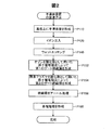
図2は、第1実施形態における半導体装置100の製造方法を示す工程図である。まず、製造者は、エピタキシャル成長によって、基板110の上にバッファ層111を形成し、その後、バッファ層111の上に半導体層114を形成する(工程P110)。
A-2. Method of Manufacturing Semiconductor Device FIG. 2 is a process chart showing a method of manufacturing the
基板110上に半導体層114を形成した後(工程P110)、製造者は、半導体層114に対してイオン注入を行うことによって、半導体層116,117,118を形成する(工程P120)。他の実施形態では、製造者は、不純物拡散および選択再成長などの他の方法を用いて、半導体層116,117,118の少なくとも1つの半導体層を形成してもよい。
After forming the
イオン注入を行った後(工程P120)、製造者は、ウェットエッチングによって半導体層114,116,117,118の各表面を処理する(工程P140)。これによって、イオン注入(工程P120)によって形成された各半導体層の損傷を除去できる。本実施形態では、製造者は、水酸化テトラメチルアンモニウム(TMAH:Tetramethylammonium hydroxide)をエッチング液として用いる。他の実施形態では、製造者は、ウェットエッチング(工程P140)を省略してもよい。 After ion implantation (process P120), the manufacturer processes each surface of the semiconductor layers 114, 116, 117, 118 by wet etching (process P140). Thereby, the damage of each semiconductor layer formed by ion implantation (process P120) can be removed. In the present embodiment, the manufacturer uses tetramethylammonium hydroxide (TMAH) as an etching solution. In another embodiment, the manufacturer may omit the wet etching (process P140).
ウェットエッチングを行った後(工程P140)、製造者は、半導体層114,116,117,118の各半導体層の上に、オゾン(O3)を酸化剤として用いた原子層堆積法(ALD:Atomic Layer Deposition)によって、第1のゲート絶縁膜131を形成する(工程P152)。本実施形態では、製造者は、半導体層114,116,117,118の各半導体層の上に、第1のゲート絶縁膜131として二酸化ケイ素(SiO2)を堆積させる。キャリア移動度の向上およびゲートリーク電流の低減を実現する観点から、第1のゲート絶縁膜131の厚さは、2nm以上20nm以下であることが好ましい。
After the wet etching (step P140), the manufacturer, on each semiconductor layer of the semiconductor layer 114,116,117,118, ozone (O 3) atomic layer deposition method using as an oxidizing agent (ALD: The first
本実施形態では、オゾン(O3)を酸化剤として用いたALD(工程P152)において、製造者は、製造途中の半導体装置100を反応室に配置した後、第1のゲート絶縁膜131が所望の厚さになるまで、次の工程a1〜a4を繰り返す。
(工程a1)反応室に原料ガスを投入
(工程a2)反応室から原料ガスをパージ
(工程a3)反応室に酸化剤としてオゾン(O3)を投入
(工程a4)反応室からオゾンをパージ
In the present embodiment, in ALD using ozone (O 3 ) as an oxidizing agent (process P152), the manufacturer places the
(Step a1) Feed the source gas into the reaction chamber (Step a2) Purge the source gas from the reaction chamber (Step a3) Feed ozone (O 3 ) as an oxidant into the reaction chamber (Step a4) Purge ozone from the reaction chamber
オゾン(O3)を酸化剤として用いたALD(工程P152)において、酸化剤のオゾン濃度は、2原子%以上30原子%以下であることが好ましい。発明者が実施した評価試験によれば、オゾン濃度が2原子%未満である場合、成膜が不安定となる傾向があり、オゾン濃度が30原子%超過である場合、膜厚が不均一になる傾向があった。本実施形態では、酸化剤のオゾン濃度は、8原子%である。 In ALD (Step P152) using ozone (O 3 ) as an oxidizing agent, the ozone concentration of the oxidizing agent is preferably 2 atomic% or more and 30 atomic% or less. According to the evaluation test conducted by the inventor, when the ozone concentration is less than 2 atomic%, the film formation tends to be unstable, and when the ozone concentration is more than 30 atomic%, the film thickness becomes uneven. Tended to In the present embodiment, the ozone concentration of the oxidant is 8 atomic%.
第1のゲート絶縁膜131を形成した後(工程P152)、製造者は、酸素プラズマを酸化剤として用いた原子層堆積法(ALD)によって、第1のゲート絶縁膜131の上に第2のゲート絶縁膜132を形成する(工程P154)。本実施形態では、製造者は、第1のゲート絶縁膜131の上に、第2のゲート絶縁膜132として二酸化ケイ素(SiO2)を堆積させる。ゲートリーク電流の低減を実現する観点から、第2のゲート絶縁膜132の厚さは、第1のゲート絶縁膜131より厚いことが好ましく、第1のゲート絶縁膜131の4倍以上であることがさらに好ましく、9倍以上であることがいっそう好ましい。
After forming the first gate insulating film 131 (process P152), the manufacturer can form a second
本実施形態では、酸素プラズマを酸化剤として用いたALD(工程P154)において、製造者は、オゾン(O3)を酸化剤として用いたALD(工程P152)に引き続き、第2のゲート絶縁膜132が所望の厚さになるまで、次の工程b1〜b5を繰り返す。
(工程b1)反応室に原料ガスを投入
(工程b2)反応室から原料ガスをパージ
(工程b3)反応室に酸化剤として酸素(O2)を投入
(工程b4)高周波電源によって反応室内にプラズマを生成
(工程b5)反応室から酸素をパージ
In the present embodiment, in the ALD using oxygen plasma as an oxidizing agent (process P154), the manufacturer continues the second
(Step b1) Raw material gas is introduced into the reaction chamber (Step b2) Purge raw material gas from the reaction chamber (Step b3) Oxygen (O 2 ) is introduced as an oxidant into the reaction chamber (Step b4) Plasma in the reaction chamber by a high frequency power source Generate oxygen (step b5) from the reaction chamber
酸素プラズマを酸化剤として用いたALD(工程P154)において、プラズマを発生させる高周波電源の電力は、200W(ワット)以上2000W以下であることが好ましい。発明者が実施した評価試験によれば、高周波電源の電力が200W未満である場合、ゲートリーク電流が増加する傾向があり、高周波電源の電力が2000W超過である場合、膜厚が不均一になる傾向があった。本実施形態では、高周波電源の電力は、500Wである。 In the ALD using oxygen plasma as an oxidizing agent (process P154), the power of the high frequency power supply for generating plasma is preferably 200 W (watt) or more and 2000 W or less. According to the evaluation test conducted by the inventor, when the power of the high frequency power supply is less than 200 W, the gate leak current tends to increase, and when the power of the high frequency power supply exceeds 2000 W, the film thickness becomes uneven. There was a tendency. In the present embodiment, the power of the high frequency power supply is 500 W.
酸素プラズマを用いたALD(工程P154)の酸化力は、オゾンを用いたALD(工程P152)より強力である。そのため、酸素プラズマを用いたALD(工程P154)の成膜率は、オゾンを用いたALD(工程P152)より高い。そのため、大気中から第2のゲート絶縁膜132に取り込まれる炭素(C)の量は、第1のゲート絶縁膜131より少なくなると考えられる。本実施形態では、オゾンを用いたALD(工程P152)の成膜率は、約3.3×10⁻²nm/サイクルであり、酸素プラズマを用いたALD(工程P154)の成膜率は、約6.6×10−2nm/サイクルである。本実施形態では、オゾンを用いたALD(工程P152)による炭素濃度は、約8.0×1021原子/cm3であり、酸素プラズマを用いたALD(工程P154)による炭素濃度は、約1.0×1021原子/cm3である。
The oxidizing power of ALD using oxygen plasma (Step P154) is stronger than ALD using ozone (Step P152). Therefore, the deposition rate of ALD using oxygen plasma (step P154) is higher than that of ALD using ozone (step P152). Therefore, the amount of carbon (C) taken into the second
第1のゲート絶縁膜131および第2のゲート絶縁膜132を形成する際(工程P152,P154)、半導体層114,116,117,118の各半導体層の温度を200℃以上600℃以下に維持することが好ましい。発明者が実施した評価試験によれば、各半導体層の温度が200℃未満である場合、ゲートリーク電流が増加する傾向があり、各半導体層の温度が600℃超過である場合、成膜途中に原料が分解するため膜厚が不均一になる傾向があった。本実施形態では、製造者は、第1のゲート絶縁膜131および第2のゲート絶縁膜132を形成する際(工程P152,P154)、製造途中の半導体装置100を載置するステージ(台)の温度を350℃に調整することによって、半導体層114,116,117,118の各半導体層の温度を350℃に維持する。
When forming the first
第2のゲート絶縁膜132を形成した後(工程P154)、製造者は、第1のゲート絶縁膜131および第2のゲート絶縁膜132に対してアニール処理(熱処理)を行う(工程P158)。第2のゲート絶縁膜132によってゲートリーク電流を十分に抑制する観点から、アニール処理(工程P158)では、第2のゲート絶縁膜132における炭素濃度を1×10¹⁹原子/cm3未満にすることが好ましい。本実施形態では、アニール処理(工程P158)によって、第1のゲート絶縁膜131における炭素濃度は、約4×1019原子/cm3になり、第2のゲート絶縁膜132における炭素濃度は、約3×1018原子/cm3になる。
After forming the second gate insulating film 132 (process P154), the manufacturer performs annealing (heat treatment) on the first
本実施形態では、アニール処理(工程P158)の温度は、300℃以上900℃以下であることが好ましい。発明者が実施した評価試験によれば、アニール処理(工程P158)の温度が300℃未満である場合、第1のゲート絶縁膜131および第2のゲート絶縁膜132に残留する炭素に起因してゲートリーク電流が増加する傾向があり、アニール処理(工程P158)の温度が900℃超過である場合、第1のゲート絶縁膜131および第2のゲート絶縁膜132の変質に起因してゲートリーク電流が増加する傾向があった。
In the present embodiment, the temperature of the annealing process (process P158) is preferably 300 ° C. or more and 900 ° C. or less. According to the evaluation test conducted by the inventor, when the temperature of the annealing process (process P158) is less than 300 ° C., due to the carbon remaining in the first
アニール処理(工程P158)を行った後、製造者は、ソース電極141と、ゲート電極142と、ドレイン電極143とを形成する(工程P180)。本実施形態では、製造者は、コンタクトホール121,123にソース電極141およびドレイン電極143を形成した後、第2のゲート絶縁膜132の上にゲート電極142を形成する。製造者は、各電極に対してアニール処理(熱処理)を行う。これらの工程を経て、半導体装置100が完成する。
After performing the annealing process (process P158), the manufacturer forms the
以上説明した第1実施形態によれば、第1のゲート絶縁膜131によって第2のゲート絶縁膜132の形成に起因するチャネル移動度の低下を抑制できるとともに、第2のゲート絶縁膜132によってゲートリーク電流を抑制できる。したがって、キャリア移動度の向上およびゲートリーク電流の低減を実現できる。
According to the first embodiment described above, the first
また、第1のゲート絶縁膜131の厚さが2nm以上20nm以下である場合、第1のゲート絶縁膜131の膜厚が不足することに起因するチャネル移動度の低下を防止するとともに、第1のゲート絶縁膜131の膜厚が過剰になることに起因するゲートリーク電流の増加を抑制することができる。
In addition, when the thickness of the first
また、第2のゲート絶縁膜132が第1のゲート絶縁膜131より厚い場合、第2のゲート絶縁膜132によってゲートリーク電流をいっそう抑制できる。
In addition, when the second
また、第1のゲート絶縁膜131および第2のゲート絶縁膜132の主成分が二酸化ケイ素(SiO2)であるため、第1のゲート絶縁膜131および第2のゲート絶縁膜132を容易に実現できる。
In addition, since the main component of the first
また、第1のゲート絶縁膜131および第2のゲート絶縁膜132を形成する際(工程P152,P154)、半導体層114,116,117,118の温度を200℃以上600℃以下に維持することによって、温度不足に起因するゲートリーク電流の増加を抑制するとともに、温度過剰に起因する第1のゲート絶縁膜131および第2のゲート絶縁膜132における膜質の低下を抑制することができる。
In addition, when forming the first
また、200W以上2000W以下の高周波電源による酸素プラズマを酸化剤として用いた原子層堆積法によって第2のゲート絶縁膜132を形成する場合(工程P154)、高周波電源の電力不足に起因するゲートリーク電流の増加を防止するとともに、高周波電源の電力過剰に起因する第2のゲート絶縁膜132における膜質の低下を抑制することができる。
When the second
また、第1のゲート絶縁膜131および第2のゲート絶縁膜132に対して300℃以上900℃以下でアニール処理(工程P158)を行うことによって、不十分なアニール処理によって第1のゲート絶縁膜131および第2のゲート絶縁膜132に残留する炭素に起因するゲートリーク電流の増加を防止するとともに、過剰なアニール処理による第1のゲート絶縁膜131および第2のゲート絶縁膜132の変質に起因するゲートリーク電流の増加を防止することができる。
In addition, by performing the annealing process (process P158) on the first
B.第2実施形態
B−1.半導体装置の構成
図3は、第2実施形態における半導体装置200の構成を模式的に示す断面図である。半導体装置200は、窒化ガリウム(GaN)を用いて形成されたGaN系の半導体装置である。本実施形態では、半導体装置200は、縦型トレンチMOSFETである。本実施形態では、半導体装置200は、電力制御に用いられ、パワーデバイスとも呼ばれる。図3には、図1と同様に、XYZ軸が図示されている。
B. Second Embodiment B-1. Configuration of Semiconductor Device FIG. 3 is a cross-sectional view schematically showing a configuration of a
半導体装置200は、基板210と、半導体層212と、半導体層214と、半導体層216とを備える。半導体装置200は、これらの半導体層212,214,216に形成された構造として、トレンチ222と、リセス224とを有する。半導体装置200は、更に、ゲート絶縁膜230と、ソース電極241と、ゲート電極242と、ドレイン電極243と、ボディ電極244とを備える。本実施形態では、半導体装置200の構造は、トレンチ222を中心に+X軸方向側と−X軸方向側とで線対称である。
The
半導体装置200の基板210は、X軸およびY軸に沿って広がる板状を成す。基板210は、窒化ガリウム(GaN)から主に成る。本実施形態では、基板210は、ケイ素(Si)をドナーとして含有する。
The
半導体装置200の半導体層212は、窒化ガリウム(GaN)から主に成るn型半導体層である。半導体層212は、基板210の+Z軸方向側に位置し、X軸およびY軸に沿って広がる層である。半導体層212は、エピタキシャル成長によって基板210の上に形成された層である。本実施形態では、半導体層212は、基板210より低い濃度でケイ素(Si)をドナーとして含有する。
The
半導体装置200の半導体層214は、窒化ガリウム(GaN)から主に成るp型半導体層である。半導体層214は、半導体層212の+Z軸方向側に位置し、X軸およびY軸に沿って広がる層である。半導体層214は、エピタキシャル成長によって半導体層212の上に形成された層である。本実施形態では、半導体層214は、マグネシウム(Mg)をアクセプタとして含有する。
The
半導体装置200の半導体層216は、窒化ガリウム(GaN)から主に成るn型半導体層である。半導体層216は、半導体層214の+Z軸方向側に位置し、X軸およびY軸に沿って広がる層である。半導体層216は、エピタキシャル成長によって半導体層214の上に形成された層である。本実施形態では、半導体層216は、半導体層212より高い濃度でケイ素(Si)をドナーとして含有する。
The
半導体装置200のトレンチ222は、半導体層212,214,216に形成され、半導体層212,214,216の厚さ方向(−Z軸方向)に落ち込んだ溝部である。トレンチ222は、半導体層216の+Z軸方向側から半導体層214を貫通し半導体層212に至る。本実施形態では、トレンチ222は、半導体層212,214,216に対するエッチングによって形成された構造である。
The
半導体装置200のゲート絶縁膜230は、電気絶縁性を有する膜である。ゲート絶縁膜230は、トレンチ222の外側から内側にわたって形成されている。ゲート絶縁膜230は、トレンチ222を画定する半導体層212,214,216の各界面と、半導体層216における+Z軸方向側の界面とを覆う。ゲート絶縁膜230は、第1のゲート絶縁膜231と、第2のゲート絶縁膜232とを備える。
The
第1のゲート絶縁膜231は、半導体層212,214,216の上に形成されている点を除き、第1実施形態における第1のゲート絶縁膜131と同様である。第1のゲート絶縁膜231は、オゾンを酸化剤として用いた原子層堆積法(ALD)によって形成された膜である。
The first
第2のゲート絶縁膜232は、第1のゲート絶縁膜231の上に形成されている点を除き、第1実施形態における第2のゲート絶縁膜132と同様である。第2のゲート絶縁膜232は、酸素プラズマを酸化剤として用いた原子層堆積法(ALD)によって形成された膜である。
The second
ゲート絶縁膜230は、コンタクトホール221を有する。コンタクトホール221は、第1のゲート絶縁膜231および第2のゲート絶縁膜232を貫通して半導体層216に至る貫通孔である。本実施形態では、コンタクトホール221は、トレンチ222より+X軸方向側および−X軸方向側の2箇所に形成されている。本実施形態では、コンタクトホール221は、ゲート絶縁膜230に対するエッチングによって形成された構造である。
The
半導体装置200のリセス224は、第1のゲート絶縁膜231、第2のゲート絶縁膜232および半導体層216を貫通して半導体層214に至るまで落ち込んだ凹部である。本実施形態では、リセス224は、トレンチ222を中心として2つのコンタクトホール221より外側の2箇所に形成されている。本実施形態では、リセス224は、ゲート絶縁膜230および半導体層214,216に対するエッチングによって形成された構造である。
The
半導体装置200のソース電極241は、コンタクトホール221に形成された電極である。ソース電極241は、半導体層216に対してオーミック接触する。本実施形態では、ソース電極241は、チタン(Ti)から成る層にアルミニウム(Al)から成る層を積層した後にアニール処理(熱処理)によって合金化した電極である。
The source electrode 241 of the
半導体装置200のゲート電極242は、ゲート絶縁膜230を介してトレンチ222に形成された電極である。本実施形態では、ゲート電極242は、アルミニウム(Al)から主に成る。ゲート電極242に電圧が印加された場合、半導体層214に反転層が形成され、この反転層がチャネルとして機能することによって、ソース電極241とドレイン電極243との間に導通経路が形成される。
The
半導体装置200のドレイン電極243は、基板210の−Z軸方向側の界面に形成された電極である。ドレイン電極243は、基板210に対してオーミック接触する。本実施形態では、ドレイン電極243は、チタン(Ti)から成る層にアルミニウム(Al)から成る層を積層した後にアニール処理(熱処理)によって合金化した電極である。
The
半導体装置200のボディ電極244は、リセス224に形成された電極である。ボディ電極244は、半導体層214にオーミック接触する。本実施形態では、ボディ電極244は、パラジウム(Pd)から成る層に金(Au)から成る層を積層した後にアニール処理(熱処理)によって合金化した電極である。
The
B−2.半導体装置の製造方法
図4は、第2実施形態における半導体装置200の製造方法を示す工程図である。まず、製造者は、エピタキシャル成長によって、基板210の上に半導体層212,214,216を順に形成する(工程P210)。
B-2. Method of Manufacturing Semiconductor Device FIG. 4 is a process chart showing a method of manufacturing the
基板210上に半導体層212,214,216を形成した後(工程P210)、製造者は、ドライエッチングによってトレンチ222を形成する(工程P230)。本実施形態では、トレンチ222を形成するドライエッチングは、誘電結合プラズマ(ICP:Inductively Coupled Plasma)ドライエッチングである。
After forming the semiconductor layers 212, 214, and 216 on the substrate 210 (process P210), the manufacturer forms the
ドライエッチングを行った後(工程P230)、製造者は、ウェットエッチングによって半導体層212,214,216の各表面を処理する(工程P240)。これによって、ドライエッチング(工程P230)によって形成された各半導体層の損傷を除去できる。本実施形態では、製造者は、水酸化テトラメチルアンモニウム(TMAH)をエッチング液として用いる。他の実施形態では、製造者は、ウェットエッチング(工程P240)を省略してもよい。 After dry etching (process P230), the manufacturer processes each surface of the semiconductor layers 212, 214, and 216 by wet etching (process P240). Thereby, damage to each semiconductor layer formed by dry etching (process P230) can be removed. In the present embodiment, the manufacturer uses tetramethyl ammonium hydroxide (TMAH) as an etching solution. In another embodiment, the manufacturer may omit the wet etching (process P240).
ウェットエッチングを行った後(工程P240)、製造者は、第1実施形態における第1のゲート絶縁膜131の形成(工程P152)と同様に、半導体層212,214,216の各半導体層の上に、オゾン(O3)を酸化剤として用いた原子層堆積法(ALD)によって、第1のゲート絶縁膜231を形成する(工程P252)。
After the wet etching (process P240), the manufacturer applies the same process as the formation of the first
第1のゲート絶縁膜231を形成した後(工程P252)、製造者は、第1実施形態における第2のゲート絶縁膜132の形成(工程P154)と同様に、酸素プラズマを酸化剤として用いた原子層堆積法(ALD)によって、第1のゲート絶縁膜231の上に第2のゲート絶縁膜232を形成する(工程P254)。
After the formation of the first gate insulating film 231 (process P252), the manufacturer used oxygen plasma as an oxidant in the same manner as the formation of the second
第2のゲート絶縁膜232を形成した後(工程P254)、製造者は、第1実施形態におけるアニール処理(工程P158)と同様に、第1のゲート絶縁膜231および第2のゲート絶縁膜232に対してアニール処理(熱処理)を行う(工程P258)。
After forming the second gate insulating film 232 (process P254), the manufacturer can process the first
アニール処理(工程P258)を行った後、製造者は、ソース電極241と、ゲート電極242と、ドレイン電極243と、ボディ電極244とを形成する(工程P280)。本実施形態では、製造者は、コンタクトホール221にソース電極241を形成し、リセス224にボディ電極244を形成し、その後、第2のゲート絶縁膜232の上にゲート電極242を形成する。その後、製造者は、基板210の上にドレイン電極243を形成する。製造者は、各電極に対してアニール処理(熱処理)を行う。これらの工程を経て、半導体装置200が完成する。
After performing the annealing process (process P258), the manufacturer forms the
以上説明した第2実施形態によれば、第1実施形態と同様に、第1のゲート絶縁膜231によって第2のゲート絶縁膜232の形成に起因するチャネル移動度の低下を抑制できるとともに、第2のゲート絶縁膜232によってゲートリーク電流を抑制できる。したがって、キャリア移動度の向上およびゲートリーク電流の低減を実現できる。また、トレンチ222に形成された第1のゲート絶縁膜231および第2のゲート絶縁膜232によって、チャネル移動度の低下を抑制するとともにゲートリーク電流を抑制することができる。
According to the second embodiment described above, similarly to the first embodiment, the first
C.第1評価試験
図5は、第1評価試験に用いた半導体装置300の構成を模式的に示す断面図である。半導体装置300は、窒化ガリウム(GaN)を用いて形成されたGaN系の半導体装置である。半導体装置300の製造方法は、第2実施形態に準ずる。図5には、図1と同様に、XYZ軸が図示されている。
C. First Evaluation Test FIG. 5 is a cross-sectional view schematically showing the configuration of the
半導体装置300は、半導体層314と、半導体層316とを備える。半導体装置300は、これらの半導体層314,316に形成された構造として、トレンチ322とリセス324とを有する。半導体装置300は、更に、ゲート絶縁膜330と、ソース電極341と、ゲート電極342と、ドレイン電極343と、ボディ電極344とを備える。
The
半導体装置300の半導体層314は、窒化ガリウム(GaN)から主に成るp型半導体層である。半導体層314は、X軸およびY軸に沿って広がる層である。半導体層314は、マグネシウム(Mg)をアクセプタとして含有する。
The
半導体装置300の半導体層316は、窒化ガリウム(GaN)から主に成るn型半導体層である。半導体層316は、半導体層314の+Z軸方向側に位置し、X軸およびY軸に沿って広がる層である。半導体層316は、エピタキシャル成長によって半導体層314の上に形成された層である。半導体層316は、ケイ素(Si)をドナーとして含有する。
The
半導体装置300のトレンチ322は、半導体層314,316に形成され、半導体層314,316の厚さ方向(−Z軸方向)に落ち込んだ溝部である。トレンチ322は、半導体層316の+Z軸方向側から半導体層314に至る。トレンチ322は、半導体層314,316に対するエッチングによって形成された構造である。
The
半導体装置300のゲート絶縁膜330は、電気絶縁性を有する膜である。ゲート絶縁膜330は、トレンチ322の外側から内側にわたって形成されている。ゲート絶縁膜330は、トレンチ322を画定する半導体層314,316の各界面と、半導体層316における+Z軸方向側の界面の一部とを覆う。ゲート絶縁膜330は、第1のゲート絶縁膜331と、第2のゲート絶縁膜332とを備える。
The
第1のゲート絶縁膜331は、半導体層314,316の上に形成されている点を除き、第1実施形態における第1のゲート絶縁膜131と同様である。第1のゲート絶縁膜331は、オゾンを酸化剤として用いた原子層堆積法(ALD)によって形成された膜である。
The first
第2のゲート絶縁膜332は、第1のゲート絶縁膜331の上に形成されている点を除き、第1実施形態における第2のゲート絶縁膜132と同様である。第2のゲート絶縁膜332は、酸素プラズマを酸化剤として用いた原子層堆積法(ALD)によって形成された膜である。
The second
半導体装置300のリセス324は、半導体層314,316に形成され、半導体層314,316の厚さ方向(−Z軸方向)に落ち込んだ凹部である。リセス324は、半導体層314,316に対するエッチングによって形成された構造である。
The
半導体装置300のソース電極341は、トレンチ322より−X軸方向側に位置し、半導体層316およびボディ電極344の上に形成された電極である。ソース電極341は、半導体層316に対してオーミック接触する。ソース電極341は、チタン(Ti)から成る層にアルミニウム(Al)から成る層を積層した後にアニール処理(熱処理)によって合金化した電極である。
The source electrode 341 of the
半導体装置300のゲート電極342は、ゲート絶縁膜330を介してトレンチ322に形成された電極である。ゲート電極342は、アルミニウム(Al)から主に成る。ゲート電極342に電圧が印加された場合、半導体層314に反転層が形成され、この反転層がチャネルとして機能することによって、ソース電極341とドレイン電極343との間に導通経路が形成される。
The
半導体装置300のドレイン電極343は、トレンチ322より+X軸方向側に位置し、半導体層316の上に形成された電極である。ドレイン電極343は、半導体層316に対してオーミック接触する。ドレイン電極343は、チタン(Ti)から成る層にアルミニウム(Al)から成る層を積層した後にアニール処理(熱処理)によって合金化した電極である。
The
半導体装置300のボディ電極344は、リセス324に形成された電極である。ボディ電極344は、半導体層314にオーミック接触する。ボディ電極344は、パラジウム(Pd)から成る層に金(Au)から成る層を積層した後にアニール処理(熱処理)によって合金化した電極である。
The
図6は、第1評価試験におけるキャリア移動度に関する評価結果を示すグラフである。図7は、第1評価試験におけるゲートリーク電流に関する評価結果を示すグラフである。第1評価試験では、試験者は、第1のゲート絶縁膜331および第2のゲート絶縁膜332の各膜厚が異なる3種類の試料S1,S2,S3,S4を10個ずつ用意した。各試料における膜厚は、次のとおりである。
FIG. 6 is a graph showing an evaluation result on carrier mobility in the first evaluation test. FIG. 7 is a graph showing an evaluation result on the gate leak current in the first evaluation test. In the first evaluation test, the tester prepared ten pieces of three types of samples S1, S2, S3, and S4 each having a different film thickness of the first
<試料S1>
第2のゲート絶縁膜332:50nm
第1のゲート絶縁膜331:0nm
<Sample S1>
Second gate insulating film 332: 50 nm
First gate insulating film 331: 0 nm
<試料S2>
第2のゲート絶縁膜332:40nm
第1のゲート絶縁膜331:10nm
<Sample S2>
Second gate insulating film 332: 40 nm
First gate insulating film 331: 10 nm
<試料S3>
第2のゲート絶縁膜332:45nm
第1のゲート絶縁膜331:5nm
<Sample S3>
Second gate insulating film 332: 45 nm
First gate insulating film 331: 5 nm
<試料S4>
第2のゲート絶縁膜332:0nm
第1のゲート絶縁膜331:50nm
<Sample S4>
Second gate insulating film 332: 0 nm
First gate insulating film 331: 50 nm
試験者は、試料S1,S2,S3についてキャリア移動度を測定し、図6の評価結果を得た。図6には、キャリア移動度について、試料の種類ごとに、最大値、最低値および平均値が示されている。図6の評価結果によれば、第1のゲート絶縁膜331によってキャリア移動度が向上することが分かる。また、第1のゲート絶縁膜331の膜厚が5nm以上である場合、10cm2/V・sを越えるキャリア移動度を確保できることが分かる。
The examiner measured the carrier mobility of the samples S1, S2, and S3 and obtained the evaluation result of FIG. FIG. 6 shows the maximum value, the minimum value, and the average value for each type of sample with respect to carrier mobility. According to the evaluation result of FIG. 6, it can be seen that the carrier mobility is improved by the first
試験者は、試料S2,S3,S4について、ゲートリーク電流が10−6A/cm2を超える際の絶縁破壊電圧を測定し、図7の評価結果を得た。図7には、絶縁破壊電圧について、試料の種類ごとに、最大値、最低値および平均値が示されている。絶縁破壊電圧の値は、大きいほどゲートリーク電流が小さくなることを示す。図7の評価試験によれば、第2のゲート絶縁膜332によって絶縁破壊電圧が向上することが分かる。言い換えると、第1のゲート絶縁膜331の上に形成された第2のゲート絶縁膜332によってゲートリーク電流を抑制できることが分かる。また、第2のゲート絶縁膜332の膜厚が5nm以上である場合、6mV/cmを越える絶縁破壊電圧を確保できることが分かる。
The tester measured the dielectric breakdown voltage when the gate leak current exceeded 10 -6 A / cm 2 for the samples S2, S3 and S4, and obtained the evaluation result of FIG. FIG. 7 shows the maximum value, the minimum value, and the average value of the breakdown voltage for each type of sample. The larger the value of the dielectric breakdown voltage, the smaller the gate leak current. According to the evaluation test of FIG. 7, it can be seen that the dielectric breakdown voltage is improved by the second
D.第2評価試験
図8は、第2評価試験に用いた試料400の構成を模式的に示す断面図である。図8には、図1と同様に、XYZ軸が図示されている。試料400は、基板410と、第1の絶縁膜431と、第2の絶縁膜432とを備える。
D. Second Evaluation Test FIG. 8 is a cross-sectional view schematically showing the configuration of the
試料400の基板410は、X軸およびY軸に沿って広がる板状を成す。基板410は、ケイ素(Si)から主に成る。基板410の厚さ(Z軸方向の長さ)は、約280μm(マイクロメートル)である。
The
試料400における第1の絶縁膜431は、基板410の上に、オゾンを酸化剤として用いた原子層堆積法(ALD)によって形成された膜である。第1の絶縁膜431は、二酸化ケイ素(SiO2)から主に成る。第1の絶縁膜431の厚さ(Z軸方向の長さ)は、100nmである。
The first
試料400における第2の絶縁膜432は、第1の絶縁膜431の上に、酸素プラズマを酸化剤として用いた原子層堆積法(ALD)によって形成された膜である。第2の絶縁膜432は、二酸化ケイ素(SiO2)から主に成る。第2の絶縁膜432の厚さ(Z軸方向の長さ)は、100nmである。
The second
図9は、第2評価試験におけるアニール処理前の元素分析結果を示すグラフである。図10は、第2評価試験におけるアニール処理後の元素分析結果を示すグラフである。試験者は、二次イオン質量分析法(SIMS:Secondary Ion Mass Spectrometry)によって、アニール処理前の試料400における第1の絶縁膜431および第2の絶縁膜432を分析し、図9の元素分析結果を得た。試験者は、SIMSによってアニール処理後の試料400における第1の絶縁膜431および第2の絶縁膜432を分析し、図10の元素分析結果を得た。第2評価試験では、アニール温度は700℃であり、アニール処理の時間は30分である。
FIG. 9 is a graph showing the results of elemental analysis before annealing in the second evaluation test. FIG. 10 is a graph showing the result of elemental analysis after annealing in the second evaluation test. The tester analyzes the first insulating
第1の絶縁膜431の炭素濃度は、アニール処理前に約1×10²⁰原子/cm3であり、アニール処理後に約4×1019原子/cm3に低下した。第1の絶縁膜431の水素濃度は、アニール処理前に約2×1021原子/cm3であり、アニール処理後に約7×1020原子/cm3に低下した。
The carbon concentration of the first insulating
第2の絶縁膜432の炭素濃度は、アニール処理前に約1×10¹⁹原子/cm3であり、アニール処理後に約3×1018原子/cm3に低下した。第2の絶縁膜432の水素濃度は、アニール処理前に約1×1021原子/cm3であり、アニール処理後に約5×1020原子/cm3に低下した。
The carbon concentration of the second
第2評価試験の結果によれば、アニール処理の前後において、炭素濃度および水素濃度ともに、第1の絶縁膜431より第2の絶縁膜432の方が低いことが分かる。また、アニール処理によって、第1の絶縁膜431および第2の絶縁膜432ともに、炭素濃度および水素濃度が低下することが分かる。また、アニール処理によって、第1の絶縁膜431では炭素濃度が19乗の桁まで低減し、第2の絶縁膜432では炭素濃度が18乗の桁まで低減することが分かる。このように、第2の絶縁膜432の炭素濃度が第1の絶縁膜431より低いため、第2の絶縁膜432は、第1の絶縁膜431よりゲートリーク電流を抑制できると考えられる。
According to the result of the second evaluation test, it can be seen that the second
また、酸素プラズマを用いた第2の絶縁膜432の炭素濃度は、アニール処理前には19乗の桁であったが、アニール処理後には18乗の桁まで低減したため、ゲートリーク電流を抑制可能になった。他方、オゾンを用いた第1の絶縁膜431の炭素濃度は、アニール処理後であっても19乗の桁に留まり、18乗の桁まで低減しなかった。このことから、炭素濃度を19乗の桁未満にまで低減可能な第2の絶縁膜432(酸素プラズマを用いて成膜された絶縁膜)を、第1の絶縁膜431(オゾンを用いて成膜された絶縁膜)の上に積層することによって、ゲートリーク電流を抑制できると考えられる。
In addition, although the carbon concentration of the second
E.他の実施形態
本発明は、上述の実施形態や実施例、変形例に限られるものではなく、その趣旨を逸脱しない範囲において種々の構成で実現することができる。例えば、発明の概要の欄に記載した各形態中の技術的特徴に対応する実施形態、実施例、変形例中の技術的特徴は、上述の課題の一部または全部を解決するために、あるいは、上述の効果の一部または全部を達成するために、適宜、差し替えや、組み合わせを行うことが可能である。また、その技術的特徴が本明細書中に必須なものとして説明されていなければ、適宜、削除することが可能である。
E. Other Embodiments The present invention is not limited to the above-described embodiments, examples, and modifications, and can be realized in various configurations without departing from the scope of the invention. For example, the technical features in the embodiments, examples, and modifications corresponding to the technical features in the respective forms described in the section of the summary of the invention are for solving some or all of the problems described above, or It is possible to replace or combine as appropriate in order to achieve part or all of the above-mentioned effects. Also, if the technical features are not described as essential in the present specification, they can be deleted as appropriate.
上述の実施形態において、基板の材質は、窒化ガリウム(GaN)、ケイ素(Si)、サファイア(Al2O3)および炭化ケイ素(SiC)などのいずれであってもよい。 In the above embodiment, the material of the substrate may be any of gallium nitride (GaN), silicon (Si), sapphire (Al 2 O 3 ), silicon carbide (SiC), and the like.
上述の実施形態において、n型半導体層に含まれるドナーは、ケイ素(Si)に限らず、ゲルマニウム(Ge)、酸素(O)などであってもよい。 In the above embodiment, the donor contained in the n-type semiconductor layer is not limited to silicon (Si), but may be germanium (Ge), oxygen (O) or the like.
上述の実施形態において、p型半導体層に含まれるアクセプタは、マグネシウム(Mg)に限らず、亜鉛(Zn)、炭素(C)などであってもよい。 In the above embodiment, the acceptor contained in the p-type semiconductor layer is not limited to magnesium (Mg), and may be zinc (Zn), carbon (C) or the like.
上述の実施形態において、ゲート絶縁膜の材質は、二酸化ケイ素(SiO2)に限らず、例えば、酸化アルミニウム(Al2O3)、酸化ハフニウム(HfO2)および酸化ジルコニウム(ZrO2)などの他の酸化膜であってもよい。上述の実施形態において、第2のゲート絶縁膜は、酸化膜に限らず、酸窒化膜(例えば、SiON、AlON、ZrONなど)、並びに、窒化膜(SiN、AlNなど)であってもよい。 In the above embodiment, the material of the gate insulating film is not limited to silicon dioxide (SiO 2 ), and other materials such as aluminum oxide (Al 2 O 3 ), hafnium oxide (HfO 2 ) and zirconium oxide (ZrO 2 ), for example It may be an oxide film of In the above embodiment, the second gate insulating film is not limited to the oxide film, and may be an oxynitride film (for example, SiON, AlON, ZrON or the like), and a nitride film (SiN, AlN or the like).
上述の実施形態において、トレンチおよびリセスを形成する手法は、ICPドライエッチングに限らず、電子サイクロトロン共鳴−反応性イオンエッチング(ECR−RIE:Electron Cyclotron Resonance - Reactive Ion Etching)など他のドライエッチングであってもよい。 In the above embodiment, the method of forming the trench and the recess is not limited to ICP dry etching, but is other dry etching such as electron cyclotron resonance-reactive ion etching (ECR-RIE). May be
上述の実施形態において、各電極の材質は、上述の材質に限らず、他の材質であってもよい。 In the above-described embodiment, the material of each electrode is not limited to the above-described material, and may be another material.
100…半導体装置
110…基板
111…バッファ層
114,116,117,118…半導体層
121,123…コンタクトホール
130…ゲート絶縁膜
131…第1のゲート絶縁膜
132…第2のゲート絶縁膜
141…ソース電極
142…ゲート電極
143…ドレイン電極
200…半導体装置
210…基板
212,214,216…半導体層
221…コンタクトホール
222…トレンチ
224…リセス
230…ゲート絶縁膜
231…第1のゲート絶縁膜
232…第2のゲート絶縁膜
241…ソース電極
242…ゲート電極
243…ドレイン電極
244…ボディ電極
300…半導体装置
314,316…半導体層
322…トレンチ
324…リセス
330…ゲート絶縁膜
331…第1のゲート絶縁膜
332…第2のゲート絶縁膜
341…ソース電極
342…ゲート電極
343…ドレイン電極
344…ボディ電極
400…試料
410…基板
431…第1の絶縁膜
432…第2の絶縁膜
100
Claims (9)
窒化ガリウム(GaN)から成る半導体層に、ドライエッチングによってトレンチを形成し、
前記ドライエッチングによって損傷した前記半導体層の表面を、TMAHによるウェットエッチングによって除去し、
前記ウェットエッチングが行なわれた前記半導体層の上に、酸化物から主に成る第1のゲート絶縁膜を、オゾンを酸化剤として用いた原子層堆積法によって形成し、
前記第1のゲート絶縁膜の上に、酸化物から主に成る第2のゲート絶縁膜を、酸素プラズマを酸化剤として用いた原子層堆積法によって形成し、
前記第2のゲート絶縁膜の上にゲート電極を形成し、
前記第1のゲート絶縁膜を形成する工程では、以下の工程a1〜a4を繰り返し、
(工程a1)反応室に原料ガスを投入
(工程a2)反応室から原料ガスをパージ
(工程a3)反応室に酸化剤としてオゾンを投入
(工程a4)反応室からオゾンをパージ
前記第2のゲート絶縁膜を形成する工程では、以下の工程b1〜b5を繰り返し、
(工程b1)反応室に原料ガスを投入
(工程b2)反応室から原料ガスをパージ
(工程b3)反応室に酸化剤として酸素を投入
(工程b4)高周波電源によって反応室内にプラズマを生成
(工程b5)反応室から酸素をパージ
前記第1のゲート絶縁膜および前記第2のゲート絶縁膜に対してアニール処理を行うことにより、前記第2のゲート絶縁膜の炭素濃度を、1×10¹⁹原子/cm3未満、かつ前記第1のゲート絶縁膜の水素濃度の低下の幅を、前記第2のゲート絶縁膜側の水素濃度の低下の幅よりも大きくし、前記半導体層のキャリア移動度は10cm2/V・sを超える、縦型トレンチMOSFETの製造方法。 A method of manufacturing a vertical trench MOSFET ,
The RaNaru Ru semiconductor layer or gallium nitride (GaN), a trench is formed by de dry etching,
The surface of the semiconductor layer damaged by previous Kido dry etching is removed by wet etching using TMAH,
A first gate insulating film mainly made of an oxide is formed on the wet-etched semiconductor layer by an atomic layer deposition method using ozone as an oxidant.
A second gate insulating film mainly made of an oxide is formed on the first gate insulating film by atomic layer deposition using oxygen plasma as an oxidant.
Forming a gate electrode on the second gate insulating film;
In the step of forming the first gate insulating film, the following steps a1 to a4 are repeated,
(Step a1) Raw material gas is introduced into the reaction chamber (Step a2) Purge raw material gas from the reaction chamber (Step a3) Ozone is introduced as an oxidant into the reaction chamber (Step a4) Purge ozone from the reaction chamber The second gate In the step of forming the insulating film, the following steps b1 to b5 are repeated,
(Step b1) Raw material gas is introduced into the reaction chamber (Step b2) Purge raw material gas from the reaction chamber (Step b3) Oxygen is introduced as an oxidant into the reaction chamber (Step b4) Plasma is generated in the reaction chamber by a high frequency power supply b5) Purge oxygen from the reaction chamber By annealing the first gate insulating film and the second gate insulating film, the carbon concentration of the second gate insulating film is 1 × 10 19 atoms. The width of the reduction of the hydrogen concentration of the first gate insulating film is less than 1 cm 3 , and the width of the reduction of the hydrogen concentration on the second gate insulating film side is larger, and the carrier mobility of the semiconductor layer is A method of manufacturing a vertical trench MOSFET exceeding 10 cm 2 / V · s.
前記第1のゲート絶縁膜を形成する前に、前記半導体層の厚さ方向に落ち込んだ溝部を前記半導体層に形成し、
前記第1のゲート絶縁膜および前記第2のゲート絶縁膜を、前記溝部の外側から内側にわたって形成する、縦型トレンチMOSFETの製造方法。 A method of manufacturing a vertical trench MOSFET according to any one of claims 1 to 3, wherein
Before forming the first gate insulating film, a groove which is sunk in the thickness direction of the semiconductor layer is formed in the semiconductor layer,
A method of manufacturing a vertical trench MOSFET , wherein the first gate insulating film and the second gate insulating film are formed from the outside to the inside of the trench .
前記アニール処理後における前記第2のゲート絶縁膜の炭素濃度は、1×10¹⁹原子/cm3未満である、請求項1から請求項8までのいずれか一項に記載の縦型トレンチMOSFETの製造方法。 The carbon concentration of the second gate insulating film before the annealing treatment is 1 × 10 19 atoms / cm 3 or more.
The vertical trench MOSFET according to any one of claims 1 to 8, wherein a carbon concentration of the second gate insulating film after the annealing process is less than 1 x 10 19 atoms / cm 3 . Production method.
Priority Applications (3)
| Application Number | Priority Date | Filing Date | Title |
|---|---|---|---|
| JP2014140520A JP6528366B2 (en) | 2014-07-08 | 2014-07-08 | Method of manufacturing vertical trench MOSFET |
| CN201510364222.6A CN105304712B (en) | 2014-07-08 | 2015-06-26 | Semiconductor device and its manufacturing method |
| US14/754,435 US9466706B2 (en) | 2014-07-08 | 2015-06-29 | Semiconductor device including first and second gate insulating films disposed on a semiconductor layer and manufacturing method of the same |
Applications Claiming Priority (1)
| Application Number | Priority Date | Filing Date | Title |
|---|---|---|---|
| JP2014140520A JP6528366B2 (en) | 2014-07-08 | 2014-07-08 | Method of manufacturing vertical trench MOSFET |
Related Child Applications (1)
| Application Number | Title | Priority Date | Filing Date |
|---|---|---|---|
| JP2019023105A Division JP2019071497A (en) | 2019-02-13 | 2019-02-13 | Semiconductor device and method of manufacturing the same |
Publications (2)
| Publication Number | Publication Date |
|---|---|
| JP2016018888A JP2016018888A (en) | 2016-02-01 |
| JP6528366B2 true JP6528366B2 (en) | 2019-06-12 |
Family
ID=55068211
Family Applications (1)
| Application Number | Title | Priority Date | Filing Date |
|---|---|---|---|
| JP2014140520A Active JP6528366B2 (en) | 2014-07-08 | 2014-07-08 | Method of manufacturing vertical trench MOSFET |
Country Status (3)
| Country | Link |
|---|---|
| US (1) | US9466706B2 (en) |
| JP (1) | JP6528366B2 (en) |
| CN (1) | CN105304712B (en) |
Families Citing this family (13)
| Publication number | Priority date | Publication date | Assignee | Title |
|---|---|---|---|---|
| WO2014185034A1 (en) * | 2013-05-13 | 2014-11-20 | パナソニックIpマネジメント株式会社 | Semiconductor device |
| JP6226004B2 (en) * | 2016-02-29 | 2017-11-08 | 富士電機株式会社 | Semiconductor device and manufacturing method of semiconductor device |
| JP6673125B2 (en) * | 2016-09-30 | 2020-03-25 | 豊田合成株式会社 | Semiconductor device |
| JP6618944B2 (en) * | 2017-03-10 | 2019-12-11 | 株式会社東芝 | Semiconductor device and electric device |
| JP7056408B2 (en) * | 2017-06-30 | 2022-04-19 | 富士電機株式会社 | Manufacturing method of gallium nitride based semiconductor device and gallium nitride based semiconductor device |
| JP7388624B2 (en) * | 2017-12-11 | 2023-11-29 | 出光興産株式会社 | Semiconductor device and semiconductor device manufacturing method |
| RU2677500C1 (en) * | 2018-03-07 | 2019-01-17 | Федеральное государственное бюджетное образовательное учреждение высшего образования "Чеченский государственный университет" | Method for making semiconductor device |
| EP3627559B1 (en) * | 2018-09-19 | 2022-06-22 | Imec Vzw | A iii-v semiconductor device and a method for forming a iii-v semiconductor device comprising an edge termination structure |
| JP7185225B2 (en) * | 2018-11-22 | 2022-12-07 | 株式会社豊田中央研究所 | Semiconductor device and method for manufacturing semiconductor device |
| CN111668189B (en) * | 2019-03-07 | 2021-09-21 | 西安电子科技大学 | Thermal electron effect test structure of MIS-HEMT device and characterization method thereof |
| JP7450446B2 (en) | 2020-04-13 | 2024-03-15 | 株式会社アドバンテスト | Semiconductor device, semiconductor device manufacturing method, and test equipment |
| JP7276247B2 (en) * | 2020-05-22 | 2023-05-18 | 豊田合成株式会社 | Semiconductor device manufacturing method |
| FR3112422B1 (en) | 2020-07-09 | 2022-08-12 | Commissariat Energie Atomique | Process for producing a dielectric layer on a structure made of III-V materials |
Family Cites Families (22)
| Publication number | Priority date | Publication date | Assignee | Title |
|---|---|---|---|---|
| US4675089A (en) * | 1985-11-25 | 1987-06-23 | At&T Technologies, Inc. | Low temperature deposition method for high quality aluminum oxide films |
| KR100400246B1 (en) * | 2000-12-29 | 2003-10-01 | 주식회사 하이닉스반도체 | Method for forming of capacitor the cell used high-integrated DRAM |
| JP2004214366A (en) * | 2002-12-27 | 2004-07-29 | Nec Electronics Corp | Semiconductor device and its fabricating process |
| WO2004093179A1 (en) * | 2003-04-17 | 2004-10-28 | Fujitsu Limited | Method for forming high dielectric film |
| JP4277268B2 (en) * | 2003-11-28 | 2009-06-10 | ローム株式会社 | Method for manufacturing metal compound thin film, and method for manufacturing semiconductor device including the metal compound thin film |
| US7067438B2 (en) * | 2004-02-19 | 2006-06-27 | Micron Technology, Inc. | Atomic layer deposition method of forming an oxide comprising layer on a substrate |
| JP3987046B2 (en) * | 2004-02-24 | 2007-10-03 | 株式会社ルネサステクノロジ | Manufacturing method of semiconductor device |
| US20070065578A1 (en) * | 2005-09-21 | 2007-03-22 | Applied Materials, Inc. | Treatment processes for a batch ALD reactor |
| EP2006888A4 (en) * | 2006-03-30 | 2011-11-09 | Mitsui Shipbuilding Eng | Method and apparatus for growing plasma atomic layer |
| JP4789713B2 (en) * | 2006-06-29 | 2011-10-12 | 株式会社豊田中央研究所 | Wet etching method, damaged layer removal method, semiconductor device manufacturing method, and semiconductor substrate manufacturing method |
| JP2008028249A (en) * | 2006-07-24 | 2008-02-07 | Matsushita Electric Ind Co Ltd | Semiconductor device, and method for manufacturing semiconductor device |
| JP2008103408A (en) | 2006-10-17 | 2008-05-01 | Furukawa Electric Co Ltd:The | Nitride compound semiconductor transistor and manufacturing method thereof |
| JP2009206312A (en) | 2008-02-28 | 2009-09-10 | Mitsui Eng & Shipbuild Co Ltd | Film deposition method and film deposition device |
| JP2010098141A (en) | 2008-10-16 | 2010-04-30 | Sumitomo Electric Device Innovations Inc | Method of manufacturing semiconductor device |
| US20130011579A1 (en) * | 2010-11-30 | 2013-01-10 | Air Products And Chemicals, Inc. | Metal-Enolate Precursors For Depositing Metal-Containing Films |
| JP5839804B2 (en) | 2011-01-25 | 2016-01-06 | 国立大学法人東北大学 | Semiconductor device manufacturing method and semiconductor device |
| WO2012127821A1 (en) * | 2011-03-23 | 2012-09-27 | パナソニック株式会社 | Semiconductor device and method for producing same |
| JP2013074069A (en) | 2011-09-27 | 2013-04-22 | Fujitsu Ltd | Semiconductor device and manufacturing method of semiconductor device |
| JP2013140866A (en) | 2012-01-04 | 2013-07-18 | Renesas Electronics Corp | Semiconductor device, and method of manufacturing the same |
| CN104094418A (en) * | 2012-02-17 | 2014-10-08 | 应用材料公司 | Passivation film stack for silicon-based solar cells |
| JP5957994B2 (en) * | 2012-03-16 | 2016-07-27 | 富士通株式会社 | Manufacturing method of semiconductor device |
| JP6011620B2 (en) * | 2012-07-13 | 2016-10-19 | 株式会社村田製作所 | Method for manufacturing transistor |
-
2014
- 2014-07-08 JP JP2014140520A patent/JP6528366B2/en active Active
-
2015
- 2015-06-26 CN CN201510364222.6A patent/CN105304712B/en active Active
- 2015-06-29 US US14/754,435 patent/US9466706B2/en active Active
Also Published As
| Publication number | Publication date |
|---|---|
| CN105304712A (en) | 2016-02-03 |
| US20160013282A1 (en) | 2016-01-14 |
| CN105304712B (en) | 2018-10-16 |
| US9466706B2 (en) | 2016-10-11 |
| JP2016018888A (en) | 2016-02-01 |
Similar Documents
| Publication | Publication Date | Title |
|---|---|---|
| JP6528366B2 (en) | Method of manufacturing vertical trench MOSFET | |
| US10026808B2 (en) | Semiconductor device including insulating film that includes negatively charged microcrystal | |
| US10153356B2 (en) | Method of manufacturing semiconductor device, and semiconductor device | |
| CN106663634B (en) | Semiconductor device and method for manufacturing semiconductor device | |
| US9548204B2 (en) | Semiconductor device, manufacturing method of the same and method of suppressing decrease of flat band voltage | |
| US9905432B2 (en) | Semiconductor device, method for manufacturing the same and power converter | |
| US20170278950A1 (en) | Method of manufacturing semiconductor device, and semiconductor device | |
| JP6011620B2 (en) | Method for manufacturing transistor | |
| CN110581068A (en) | Method for realizing low-on-resistance enhanced gallium nitride transistor by using gate dielectric | |
| JP6732821B2 (en) | Method of manufacturing semiconductor device | |
| JP2019071497A (en) | Semiconductor device and method of manufacturing the same | |
| US10177234B2 (en) | Semiconductor device | |
| US10153352B2 (en) | Semiconductor device | |
| US9852925B2 (en) | Method of manufacturing semiconductor device | |
| JP6658431B2 (en) | Semiconductor device | |
| US9831311B2 (en) | Semiconductor device and method of manufacturing the same | |
| JP6327139B2 (en) | Semiconductor device and manufacturing method thereof | |
| US9966447B2 (en) | Method of manufacturing semiconductor device by plasma treatment and heat treatment, and semiconductor device | |
| JP2015198210A (en) | Semiconductor device and manufacturing method of the same |
Legal Events
| Date | Code | Title | Description |
|---|---|---|---|
| A621 | Written request for application examination |
Free format text: JAPANESE INTERMEDIATE CODE: A621 Effective date: 20160823 |
|
| A977 | Report on retrieval |
Free format text: JAPANESE INTERMEDIATE CODE: A971007 Effective date: 20170511 |
|
| A131 | Notification of reasons for refusal |
Free format text: JAPANESE INTERMEDIATE CODE: A131 Effective date: 20170606 |
|
| A521 | Request for written amendment filed |
Free format text: JAPANESE INTERMEDIATE CODE: A523 Effective date: 20170802 |
|
| A131 | Notification of reasons for refusal |
Free format text: JAPANESE INTERMEDIATE CODE: A131 Effective date: 20171219 |
|
| A521 | Request for written amendment filed |
Free format text: JAPANESE INTERMEDIATE CODE: A523 Effective date: 20180214 |
|
| A131 | Notification of reasons for refusal |
Free format text: JAPANESE INTERMEDIATE CODE: A131 Effective date: 20180529 |
|
| A521 | Request for written amendment filed |
Free format text: JAPANESE INTERMEDIATE CODE: A523 Effective date: 20180726 |
|
| A02 | Decision of refusal |
Free format text: JAPANESE INTERMEDIATE CODE: A02 Effective date: 20181113 |
|
| A521 | Request for written amendment filed |
Free format text: JAPANESE INTERMEDIATE CODE: A523 Effective date: 20190213 |
|
| A911 | Transfer to examiner for re-examination before appeal (zenchi) |
Free format text: JAPANESE INTERMEDIATE CODE: A911 Effective date: 20190220 |
|
| TRDD | Decision of grant or rejection written | ||
| A01 | Written decision to grant a patent or to grant a registration (utility model) |
Free format text: JAPANESE INTERMEDIATE CODE: A01 Effective date: 20190416 |
|
| A61 | First payment of annual fees (during grant procedure) |
Free format text: JAPANESE INTERMEDIATE CODE: A61 Effective date: 20190429 |
|
| R150 | Certificate of patent or registration of utility model |
Ref document number: 6528366 Country of ref document: JP Free format text: JAPANESE INTERMEDIATE CODE: R150 |